US10692450B2 - Display panel, display device, and driving method - Google Patents
Display panel, display device, and driving method Download PDFInfo
- Publication number
- US10692450B2 US10692450B2 US15/994,937 US201815994937A US10692450B2 US 10692450 B2 US10692450 B2 US 10692450B2 US 201815994937 A US201815994937 A US 201815994937A US 10692450 B2 US10692450 B2 US 10692450B2
- Authority
- US
- United States
- Prior art keywords
- pixels
- groups
- column
- unit
- data
- Prior art date
- Legal status (The legal status is an assumption and is not a legal conclusion. Google has not performed a legal analysis and makes no representation as to the accuracy of the status listed.)
- Active, expires
Links
Images


Classifications
-
- G—PHYSICS
- G09—EDUCATION; CRYPTOGRAPHY; DISPLAY; ADVERTISING; SEALS
- G09G—ARRANGEMENTS OR CIRCUITS FOR CONTROL OF INDICATING DEVICES USING STATIC MEANS TO PRESENT VARIABLE INFORMATION
- G09G3/00—Control arrangements or circuits, of interest only in connection with visual indicators other than cathode-ray tubes
- G09G3/20—Control arrangements or circuits, of interest only in connection with visual indicators other than cathode-ray tubes for presentation of an assembly of a number of characters, e.g. a page, by composing the assembly by combination of individual elements arranged in a matrix no fixed position being assigned to or needed to be assigned to the individual characters or partial characters
- G09G3/34—Control arrangements or circuits, of interest only in connection with visual indicators other than cathode-ray tubes for presentation of an assembly of a number of characters, e.g. a page, by composing the assembly by combination of individual elements arranged in a matrix no fixed position being assigned to or needed to be assigned to the individual characters or partial characters by control of light from an independent source
- G09G3/36—Control arrangements or circuits, of interest only in connection with visual indicators other than cathode-ray tubes for presentation of an assembly of a number of characters, e.g. a page, by composing the assembly by combination of individual elements arranged in a matrix no fixed position being assigned to or needed to be assigned to the individual characters or partial characters by control of light from an independent source using liquid crystals
- G09G3/3611—Control of matrices with row and column drivers
- G09G3/3614—Control of polarity reversal in general
-
- G—PHYSICS
- G02—OPTICS
- G02F—OPTICAL DEVICES OR ARRANGEMENTS FOR THE CONTROL OF LIGHT BY MODIFICATION OF THE OPTICAL PROPERTIES OF THE MEDIA OF THE ELEMENTS INVOLVED THEREIN; NON-LINEAR OPTICS; FREQUENCY-CHANGING OF LIGHT; OPTICAL LOGIC ELEMENTS; OPTICAL ANALOGUE/DIGITAL CONVERTERS
- G02F1/00—Devices or arrangements for the control of the intensity, colour, phase, polarisation or direction of light arriving from an independent light source, e.g. switching, gating or modulating; Non-linear optics
- G02F1/01—Devices or arrangements for the control of the intensity, colour, phase, polarisation or direction of light arriving from an independent light source, e.g. switching, gating or modulating; Non-linear optics for the control of the intensity, phase, polarisation or colour
- G02F1/13—Devices or arrangements for the control of the intensity, colour, phase, polarisation or direction of light arriving from an independent light source, e.g. switching, gating or modulating; Non-linear optics for the control of the intensity, phase, polarisation or colour based on liquid crystals, e.g. single liquid crystal display cells
- G02F1/133—Constructional arrangements; Operation of liquid crystal cells; Circuit arrangements
- G02F1/1333—Constructional arrangements; Manufacturing methods
- G02F1/1343—Electrodes
- G02F1/134309—Electrodes characterised by their geometrical arrangement
-
- G—PHYSICS
- G02—OPTICS
- G02F—OPTICAL DEVICES OR ARRANGEMENTS FOR THE CONTROL OF LIGHT BY MODIFICATION OF THE OPTICAL PROPERTIES OF THE MEDIA OF THE ELEMENTS INVOLVED THEREIN; NON-LINEAR OPTICS; FREQUENCY-CHANGING OF LIGHT; OPTICAL LOGIC ELEMENTS; OPTICAL ANALOGUE/DIGITAL CONVERTERS
- G02F1/00—Devices or arrangements for the control of the intensity, colour, phase, polarisation or direction of light arriving from an independent light source, e.g. switching, gating or modulating; Non-linear optics
- G02F1/01—Devices or arrangements for the control of the intensity, colour, phase, polarisation or direction of light arriving from an independent light source, e.g. switching, gating or modulating; Non-linear optics for the control of the intensity, phase, polarisation or colour
- G02F1/13—Devices or arrangements for the control of the intensity, colour, phase, polarisation or direction of light arriving from an independent light source, e.g. switching, gating or modulating; Non-linear optics for the control of the intensity, phase, polarisation or colour based on liquid crystals, e.g. single liquid crystal display cells
- G02F1/133—Constructional arrangements; Operation of liquid crystal cells; Circuit arrangements
- G02F1/136—Liquid crystal cells structurally associated with a semi-conducting layer or substrate, e.g. cells forming part of an integrated circuit
- G02F1/1362—Active matrix addressed cells
- G02F1/136286—Wiring, e.g. gate line, drain line
-
- G—PHYSICS
- G02—OPTICS
- G02F—OPTICAL DEVICES OR ARRANGEMENTS FOR THE CONTROL OF LIGHT BY MODIFICATION OF THE OPTICAL PROPERTIES OF THE MEDIA OF THE ELEMENTS INVOLVED THEREIN; NON-LINEAR OPTICS; FREQUENCY-CHANGING OF LIGHT; OPTICAL LOGIC ELEMENTS; OPTICAL ANALOGUE/DIGITAL CONVERTERS
- G02F1/00—Devices or arrangements for the control of the intensity, colour, phase, polarisation or direction of light arriving from an independent light source, e.g. switching, gating or modulating; Non-linear optics
- G02F1/01—Devices or arrangements for the control of the intensity, colour, phase, polarisation or direction of light arriving from an independent light source, e.g. switching, gating or modulating; Non-linear optics for the control of the intensity, phase, polarisation or colour
- G02F1/13—Devices or arrangements for the control of the intensity, colour, phase, polarisation or direction of light arriving from an independent light source, e.g. switching, gating or modulating; Non-linear optics for the control of the intensity, phase, polarisation or colour based on liquid crystals, e.g. single liquid crystal display cells
- G02F1/133—Constructional arrangements; Operation of liquid crystal cells; Circuit arrangements
- G02F1/136—Liquid crystal cells structurally associated with a semi-conducting layer or substrate, e.g. cells forming part of an integrated circuit
- G02F1/1362—Active matrix addressed cells
- G02F1/1368—Active matrix addressed cells in which the switching element is a three-electrode device
-
- G—PHYSICS
- G09—EDUCATION; CRYPTOGRAPHY; DISPLAY; ADVERTISING; SEALS
- G09G—ARRANGEMENTS OR CIRCUITS FOR CONTROL OF INDICATING DEVICES USING STATIC MEANS TO PRESENT VARIABLE INFORMATION
- G09G3/00—Control arrangements or circuits, of interest only in connection with visual indicators other than cathode-ray tubes
- G09G3/20—Control arrangements or circuits, of interest only in connection with visual indicators other than cathode-ray tubes for presentation of an assembly of a number of characters, e.g. a page, by composing the assembly by combination of individual elements arranged in a matrix no fixed position being assigned to or needed to be assigned to the individual characters or partial characters
- G09G3/2003—Display of colours
-
- G—PHYSICS
- G09—EDUCATION; CRYPTOGRAPHY; DISPLAY; ADVERTISING; SEALS
- G09G—ARRANGEMENTS OR CIRCUITS FOR CONTROL OF INDICATING DEVICES USING STATIC MEANS TO PRESENT VARIABLE INFORMATION
- G09G3/00—Control arrangements or circuits, of interest only in connection with visual indicators other than cathode-ray tubes
- G09G3/20—Control arrangements or circuits, of interest only in connection with visual indicators other than cathode-ray tubes for presentation of an assembly of a number of characters, e.g. a page, by composing the assembly by combination of individual elements arranged in a matrix no fixed position being assigned to or needed to be assigned to the individual characters or partial characters
- G09G3/34—Control arrangements or circuits, of interest only in connection with visual indicators other than cathode-ray tubes for presentation of an assembly of a number of characters, e.g. a page, by composing the assembly by combination of individual elements arranged in a matrix no fixed position being assigned to or needed to be assigned to the individual characters or partial characters by control of light from an independent source
- G09G3/36—Control arrangements or circuits, of interest only in connection with visual indicators other than cathode-ray tubes for presentation of an assembly of a number of characters, e.g. a page, by composing the assembly by combination of individual elements arranged in a matrix no fixed position being assigned to or needed to be assigned to the individual characters or partial characters by control of light from an independent source using liquid crystals
- G09G3/3611—Control of matrices with row and column drivers
- G09G3/3685—Details of drivers for data electrodes
- G09G3/3688—Details of drivers for data electrodes suitable for active matrices only
-
- G—PHYSICS
- G02—OPTICS
- G02F—OPTICAL DEVICES OR ARRANGEMENTS FOR THE CONTROL OF LIGHT BY MODIFICATION OF THE OPTICAL PROPERTIES OF THE MEDIA OF THE ELEMENTS INVOLVED THEREIN; NON-LINEAR OPTICS; FREQUENCY-CHANGING OF LIGHT; OPTICAL LOGIC ELEMENTS; OPTICAL ANALOGUE/DIGITAL CONVERTERS
- G02F2201/00—Constructional arrangements not provided for in groups G02F1/00 - G02F7/00
- G02F2201/12—Constructional arrangements not provided for in groups G02F1/00 - G02F7/00 electrode
- G02F2201/121—Constructional arrangements not provided for in groups G02F1/00 - G02F7/00 electrode common or background
-
- G—PHYSICS
- G02—OPTICS
- G02F—OPTICAL DEVICES OR ARRANGEMENTS FOR THE CONTROL OF LIGHT BY MODIFICATION OF THE OPTICAL PROPERTIES OF THE MEDIA OF THE ELEMENTS INVOLVED THEREIN; NON-LINEAR OPTICS; FREQUENCY-CHANGING OF LIGHT; OPTICAL LOGIC ELEMENTS; OPTICAL ANALOGUE/DIGITAL CONVERTERS
- G02F2201/00—Constructional arrangements not provided for in groups G02F1/00 - G02F7/00
- G02F2201/12—Constructional arrangements not provided for in groups G02F1/00 - G02F7/00 electrode
- G02F2201/123—Constructional arrangements not provided for in groups G02F1/00 - G02F7/00 electrode pixel
-
- G—PHYSICS
- G09—EDUCATION; CRYPTOGRAPHY; DISPLAY; ADVERTISING; SEALS
- G09G—ARRANGEMENTS OR CIRCUITS FOR CONTROL OF INDICATING DEVICES USING STATIC MEANS TO PRESENT VARIABLE INFORMATION
- G09G2310/00—Command of the display device
- G09G2310/02—Addressing, scanning or driving the display screen or processing steps related thereto
- G09G2310/0264—Details of driving circuits
- G09G2310/0297—Special arrangements with multiplexing or demultiplexing of display data in the drivers for data electrodes, in a pre-processing circuitry delivering display data to said drivers or in the matrix panel, e.g. multiplexing plural data signals to one D/A converter or demultiplexing the D/A converter output to multiple columns
Definitions
- the present application relates to the field of display technologies, and in particular, to a display panel, a display device, and a driving method.
- liquid crystal display panels are becoming thinner and lighter, and the power consumption is getting lower.
- the common polarity inversion methods include: frame inversion, column inversion, line inversion, and point inversion.
- frame inversion, line inversion, or column inversion it appears that all sub-pixels having a certain color will be charged at a voltage with one polarity when a certain frame is displayed, and when the next frame is displayed these sub-pixels will then be charged at the same time at with the voltage with another polarity. This switch can result in a flicker phenomenon occurring when switching between two frames of images, thereby affecting the display effect.
- the present disclosure provides a display panel, a display device, and a driving method, which are used to avoid flickering of a display image and thus improve the display quality.
- the present disclosure provides a display panel.
- the display panel includes N pixel column unit groups.
- Each of the N pixel column unit groups includes a first pixel column unit and a second pixel column unit.
- Each of the first pixel column unit and the second pixel column unit includes a first column of pixels, a second column of pixels, a third column of pixels, and a fourth column of pixels. All colors of pixels of the first column of pixels are identical to all colors of pixels of the third column of pixels and all colors of pixels of the second column of pixels are identical to all colors of pixels of the fourth column of pixels.
- Pixels in the N pixel column unit groups includes first color pixels, second color pixels, third color pixels, and fourth color pixels.
- the display panel further includes N data line unit groups corresponding to the N pixel column unit groups in one-to-one correspondence.
- Each of the N data line unit groups includes a first data line unit and a second data line unit.
- Each of the first data line unit and the second data line unit includes four data lines.
- the four data lines in the first data line unit of each of the N data line unit groups are electrically connected to the first column of pixels, the second column of pixels, the third column of pixels, and the fourth column of pixels in the first pixel column unit of a corresponding pixel column unit group of the N pixel column unit group in one-to-one correspondence
- the four data lines in the second data line unit of each of the N data line unit groups are electrically connected to the first column of pixels, the second column of pixels, the third column of pixels, and the fourth column of pixels in the second pixel column unit of a corresponding pixel column unit group of the N pixel column unit group in one-to-one correspondence.
- the display panel further includes N driving unit groups corresponding to the N data line unit groups in one-to-one correspondence.
- Each of the N driving unit groups includes a first driving unit and a second driving unit, and each of the first driving unit and the second driving unit includes four switch element groups, each of which has a first terminal and a second terminal.
- the first terminals of the four switch element groups in the first driving unit of each of the N driving unit groups are electrically connected to said four data lines in the first data line unit of a corresponding data line unit group of the N data line unit groups in one-to-one correspondence
- first terminals of the four switch element groups in the second driving unit of each of the N driving unit groups are electrically connected to said four data lines in a second data line unit of a corresponding data line unit group of the N data line unit groups in one-to-one correspondence.
- the display panel further includes N data output groups corresponding to the N driving unit groups in one-to-one correspondence.
- Each of the N data output groups includes a first data output and a second data output, and a polarity of a data signal output from the first data output is opposite to a polarity of a data signal output from the second data output.
- the second terminals of two switch element groups in the first driving unit of each of the N driving unit groups are electrically connected to the first data output of a corresponding data output group of the N data output groups, and the second terminals of the other two switch element groups in the first driving unit of each of the N driving unit groups are electrically connected to the second data output of the corresponding data output group of the N data output groups.
- At least one color of pixels in one column of two columns of pixels corresponding to the two switch element groups of the first driving unit connected to the first data output are different from at least one color of pixels in the other one column of the two columns of pixels corresponding to the two switch element groups of the first driving unit connected to the first data output, and at least one color of pixels of one column of the other two columns of pixels corresponding to the other two switch element groups of the first driving unit connected to the second data output are different from at least one color of pixels of the other one column of the other two columns of pixels corresponding to the other two switch element groups of the first driving unit connected to the second data output.
- the second terminals of two switch element groups in the second driving unit of each of the N driving unit groups are electrically connected to the first data output of a corresponding data output group of the N data output groups, and the second terminals of the other two switch element groups in the second driving unit of each of the N driving unit groups are electrically connected to the second data output of the corresponding data output group of the N data output groups.
- At least one color of pixels in one column of two columns of pixels corresponding to the two switch element groups of the second driving unit connected to the first data output are different from at least one color of pixels in the other one column of the two columns of pixels corresponding to the two switch element groups of the second driving unit connected to the first data output, and at least one color of pixels in one column of the other two columns of pixels corresponding to the other two switch element groups of the second driving unit connected to the second data output are different from at least one color of pixels in the other one column of the other two columns of pixels corresponding to the other two switch element groups of the second driving unit connected to the second data output.
- N is a positive integer.
- the present disclosure provides a display device, and the display device includes the abovementioned display panel.
- the present disclosure provides a driving method for the abovementioned display panel.
- the driving method for the display panel includes steps of: providing the first data output and the second data output of each of the N data output groups with data signals having opposite polarities; and providing an enable signal to the four switch element groups in the first driving unit and the four switch element groups in the second driving unit of each of the N driving unit groups, so that a first terminal and a second terminal of each of the four switch element groups in the first driving unit and the four switch element groups in the second driving unit of each of the N driving unit groups are switched on, and the data signals are transmitted to respective columns of pixel.
- FIG. 1 is a structural cross sectional diagram of a display panel according to an embodiment of the present disclosure
- FIG. 2 is a top view of a structural schematic diagram of a display panel according to an embodiment of the present disclosure
- FIG. 3 is still a top view of another structural schematic diagram of a display panel according to an embodiment of the present disclosure.
- FIG. 4 is a flowchart of a driving method for a display panel according to an embodiment of the present disclosure
- FIG. 5 is still a top view of another structural schematic diagram of a display panel according to an embodiment of the present disclosure.
- FIG. 6 is still a top view of another structural schematic diagram of a display panel according to an embodiment of the present disclosure.
- FIG. 7 is a time sequence of signals driving a display panel according to an embodiment of the present disclosure.
- FIG. 8 is still a top view of another structural schematic diagram of a display panel according to an embodiment of the present disclosure.
- FIG. 9 is still a top view of another structural schematic diagram of a display panel according to an embodiment of the present disclosure.
- FIG. 10 is still a top view of another structural schematic diagram of a display panel according to an embodiment of the present disclosure.
- FIG. 11 is still a top view of another structural schematic diagram of a display panel according to an embodiment of the present disclosure.
- FIG. 12 is another time sequence of signals driving a display panel according to an embodiment of the present disclosure.
- FIG. 13 is still a top view of another structural schematic diagram of a display panel according to an embodiment of the present disclosure.
- FIG. 14 is still a top view of another structural schematic diagram of a display panel according to an embodiment of the present disclosure.
- FIG. 15 is still a top view of another structural schematic diagram of a display panel according to an embodiment of the present disclosure.
- FIG. 16 is a time sequence of signals driving a display panel according to an embodiment of the present disclosure.
- FIG. 17 is a structural schematic diagram of a display device according to an embodiment of the present disclosure.
- a first color pixel may also be referred to as a second color pixel, similarly, a second color pixel may also be referred to as a first color pixel.
- FIG. 1 it is a structural schematic diagram of a display panel according to an embodiment of the present disclosure.
- the display panel 100 in the embodiments can be understood as a liquid crystal display panel, and the liquid crystal display panel includes an array substrate 62 , a color film substrate 61 disposed opposite to the array substrate 62 , and a liquid crystal layer 63 disposed between the array substrate 62 and the color film substrate 61 .
- the array substrate 62 is provided thereon with a plurality of pixels (not shown) defined by a plurality of rows of gate lines (not shown) intersecting a plurality of columns of data lines (not shown).
- each pixel is provided therein with a thin film transistor (not shown), a pixel electrode (not shown) and a common electrode (not shown).
- Each thin film transistor has a gate electrode connected to a gate line, a source electrode connected to a data line, and a drain electrode connected to a pixel electrode. Under the control of the corresponding gate line, a data line corresponding to the source electrode of the thin film transistor performs charging and discharging on the pixel electrode corresponding to the drain electrode through the thin film transistor, and an electric field is formed between the pixel electrode and the common electrode.
- the common electrode receives a common electrical signal (usually a constant voltage signal), and an electric field is formed between the pixel electrode and the common electrode, which controls deflection of liquid crystal molecules in the liquid crystal layer, so as to allow light of the backlight to be transmitted, thereby achieving the display function.
- a common electrical signal usually a constant voltage signal
- FIG. 2 is another structural schematic diagram of a display panel according to an embodiment of the present disclosure
- the display panel 100 includes a first color pixel 1011 , a second color pixel 1012 , a third color pixel 1013 and a fourth color pixel 1014 .
- FIG. 2 exemplarily shows one arrangement manner.
- the display panel 100 further includes N pixel column unit groups 13 .
- Each pixel column unit group 13 includes a first pixel column unit 131 and a second pixel column unit 132 .
- the first pixel column unit 131 and the second pixel column unit 132 each includes a first column of pixels 1301 , a second column of pixels 1302 , a third column of pixels 1303 , and a fourth column of pixels 1304 .
- Color(s) of pixel(s) included in the first column of pixels 1301 is/are the same as color(s) of pixel(s) included in the third column of pixels 1303 .
- both the first column of pixels 1301 and the third column of pixels 1303 are composed of pixel(s) having a same color.
- both the first column of pixels 1301 and the third column of pixels 1303 include pixels having more than one colors, and the pixels included in the first column of pixels 1301 and the pixels included in the third column of pixels 1303 correspond to the same colors.
- both the first column of pixels 1301 and the third column of pixels 1303 include pixels having two colors.
- Color(s) of pixel(s) included in the second column of pixels 1302 is/are the same as color(s) of pixel(s) included in the fourth column of pixels 1304 , and for understanding of the second column of pixels 1302 and the fourth column of pixels 1304 , reference can be made to the first column of pixels 1301 and the third column of pixels 1303 , which will not be further described herein.
- the display panel 100 further includes N data line unit groups 15 one-to-one corresponding to the N pixel column unit groups 13 .
- Each of the N data line unit groups 15 includes a first data line unit 151 and a second data line unit 152 .
- Each of the first data line unit 151 and the second data line unit 152 includes four data lines 150 .
- the four data lines 150 in the first data line unit 151 are electrically connected to the four pixel columns in the first pixel column unit 131 in one-to-one correspondence.
- the four data lines 150 in the second data line unit 152 are electrically connected to the four pixel columns in the second pixel column unit 132 in one-to-one correspondence.
- the display panel 100 further includes N driving unit groups 17 one-to-one corresponding to the N data line unit groups 15 .
- Each of the N driving unit groups 17 includes a first driving unit 171 and a second driving unit 172 .
- Each of the first driving unit 171 and the second driving unit 172 includes four switch element groups 170 .
- First terminals of the four switch element groups 170 in the first driving unit 171 are electrically connected to the four data lines 150 in the first data line unit 151 in one-to-one correspondence.
- First terminals of the four switch element groups 170 in the second driving unit 172 are electrically connected to the four data lines 150 in the second data line unit 152 in one-to-one correspondence.
- the display panel 100 further includes N data output groups 19 corresponding to the N driving unit groups 17 .
- Each of the N data output groups 19 includes a first data output 191 and a second data output 192 .
- a polarity of a data signal output from the first data output 191 is opposite to a polarity of a data signal output from the second data output 192 .
- the polarity of the data signal output from the first data output 191 is positive, and the polarity of the data signal output from the second data output 192 is negative.
- the polarity of the data signal output from the first data output 191 is negative, and the polarity of the data signal output from the second data output 192 is positive.
- This embodiment does not limit the polarities of the data signals output from the above two data outputs as long as the polarity of the data signal output from the first data output is opposite to the polarity of the data signal output from the second data output.
- the second terminals of two of the four switch element groups 170 in the first driving unit 171 are electrically connected to the first data output 191 , and two pixel columns corresponding to the two switch element groups 170 connected to the first data output 191 have pixels of different colors.
- the second terminals of the other two of the four switch element groups 170 in the first driving unit 171 are electrically connected to the second data output 192 , and the two pixel columns corresponding to the other two switch element groups 170 connected to the second data output 192 have pixels of different colors.
- the second terminals of two of the four switch element groups 170 in the second driving unit 172 are electrically connected to the first data output 191 , and two pixel columns corresponding to the two switch element groups 170 connected to the first data output 191 have pixels of different colors.
- the second terminals of the other two of the four switch element groups 170 in the second driving unit 172 are electrically connected to the second data output 192 , and the other two pixel columns corresponding to the two switch element groups 170 connected to the second data output 192 have pixels of different colors, wherein N is a positive integer.
- the deflection of the liquid crystal molecules is determined by the common voltage signal received by the common electrode and the data signal received by the pixel electrode.
- the common electrode generally receives a constant electrical signal (for example, a voltage value of the constant electrical signal is a)
- voltage value b of the data signal received by the pixel electrode is larger than the voltage value a of the electrical signal received by the common electrode, it indicates that the polarity of the data signal is positive, that is, the polarity of the data signal received by the corresponding pixel is positive. Otherwise, the polarity of the data signal is negative, and the polarity of the data signal received by the corresponding pixel is negative.
- the polarity of the data signal received by some red pixels may be positive, and the polarity of the data signal received by other red pixels may be negative.
- the deflection angles of the liquid crystal molecules have a same value, and the difference lies in that some liquid crystal molecules are deflected clockwise, and some other liquid crystal molecules are deflected counterclockwise. Since the deflection angles of the liquid crystal molecules have a certain value, the light-transmittance amounts from the backlight have a certain value, and thus the image displaying effect will not be influenced.
- the clockwise deflection of the liquid crystal molecules corresponds to the positive polarity
- the counterclockwise deflection of the liquid crystal molecules corresponds to the negative polarity. That is, in the process of displaying a solid color image, pixels having a same color are divided into two parts, the polarity of the data signal received by one of the two parts is positive, and the polarity of the data signal received by the other one of the two parts is negative.
- the polarity of the data signal received by some pixels is positive while the polarity of the data signal received by other pixels having this color is negative, thereby avoiding a flickering phenomenon caused by significant non-uniform brightness due to all pixels having a same color changing from one polarity to another polarity for the entire image, which can improve the display quality.
- polarities are different, liquid crystal has a same deflection angle, and thus will not influence the display effect.
- first period of polarity inversion can be understood as a frame time
- second period of polarity inversion can also be understood as a frame time
- from the first period of polarity inversion to the second period of polarity inversion can be understood as “from the current frame to the next frame”.
- the polarity of the data signal output from the first data output in the current frame is opposite to the polarity of the data signal output from the first data output in the next frame.
- the polarity of the data signal output from the second data output in the current frame is also opposite to the polarity of the data signal output from the second data output in the next frame.
- FIG. 3 is still another structural schematic diagram of a display panel according to an embodiment of the present disclosure.
- two red pixel columns (the first column of pixels 1301 and the third column of pixels 1303 ) in the first pixel column unit 131 receive data signals with opposite polarities, that is, the polarity of the data signal received by the first column of pixels 1301 is positive, and the polarity of the data signal received by the third column of pixels 1303 is negative.
- the polarity inversion process according to this embodiment will be exemplified by using a polarity inversion cycle as one frame.
- some red pixels receive a data signal having a positive polarity
- other red pixels receive a data signal having a negative polarity
- some red pixels that have received the data signal having the positive polarity receive the data signal having a negative polarity
- the other red pixels that have received the data signal having the negative polarity receive the data signal having a positive polarity.
- the data signal received by some red pixels changes from a first signal (which can be understood as the polarity of the data signal is positive) to a second signal (the polarity of the data signal is negative), and the data signal received by the other red pixels changes from the second signal (the polarity of the data signal is negative) to the first signal (the polarity of the data signal is positive).
- the polarity of the data signal received by some of pixels of a same color is positive
- the polarity of the data signal received by some of the pixels of the same color is negative.
- this embodiment can avoid the flickering phenomenon caused by significant non-uniform brightness due to all pixels having a same color changing from one polarity to another polarity for the entire image while switching between two adjacent frames of images, thereby improving the display quality.
- first data output 191 and the second data output 192 included in the data output group 19 involved in this embodiment are both driven by a driving chip. That is, the data signals received by the pixels are provided by the driving chip.
- this embodiment provides a driving method for a display panel, and the driving method for the display panel is applicable to the abovementioned display panel 100 .
- FIG. 4 is a flowchart of a driving method for a display panel according to an embodiment of the present disclosure, and the driving method for the display panel includes the following steps.
- the first data output and the second data output are provided with data signals having opposite polarities.
- an enable signal is provided to the switch element groups, so that the first and second terminals of each switch element group are switched on and the data signals are transmitted to respective columns of pixels.
- the driving method for the display panel will be described by taking the first color pixel 1011 shown in FIG. 2 as an example.
- the polarity of the data signal output from the first data output 191 is positive, and the polarity of the data signal output from the second data output is negative.
- the first column of pixels 1301 and the second column of pixels 1302 respectively electrically connected to the first data output 191 receive a data signal having a positive polarity, that is, the polarity of the data signal received by the first color pixel 1011 disposed in the first column of pixels 1301 is positive.
- the third column of pixels 1303 and the fourth column of pixels 1304 respectively electrically connected to the second data output 192 receives a data signal having a negative polarity, that is, the polarity of the data signal received by the first color pixel 1011 disposed in the third column of pixels 1303 is negative.
- the first column of pixels 1301 and the second column of pixels 1302 respectively electrically connected to the first data output 191 receives a data signal having a positive polarity, that is, the polarity of the data signal received by the first color pixel 1011 disposed in the first column of pixels 1301 is positive.
- the third column of pixels 1303 and the fourth column of pixels 1304 respectively electrically connected to the second data output 192 receives a data signal having a negative polarity, that is, the polarity of the data signal received by the first color pixel 1011 disposed in the third column of pixels 1303 is negative. That is, in the current frame, the polarity of the data signal received by some first color pixels 1011 is positive, and the polarity of the data signal received by some other first color pixels 1011 is negative.
- the polarity of the data signal output from the first data output 191 becomes negative, and the polarity of the data signal output from the second data output 192 becomes positive.
- the first pixel column unit 131 the first column of pixels 1301 and the second column of pixels 1302 respectively electrically connected to the first data output 191 receives a data signal having a negative polarity, that is, the polarity of the data signal received by the first color pixel 1011 disposed in the first column of pixels 1301 is negative.
- the third column of pixels 1303 and the fourth column of pixels 1304 respectively electrically connected to the second data output 192 receives a data signal having a positive polarity, that is, the polarity of the data signal received by the first color pixel 1011 disposed in the third column of pixels 1303 is positive.
- the first column of pixels 1301 and the second column of pixels 1302 respectively electrically connected to the first data output 191 receives a data signal having a negative polarity, that is, the polarity of the data signal received by the first color pixel 1011 disposed in the first column of pixels 1301 is negative.
- the third column of pixels 1303 and the fourth column of pixels 1304 respectively electrically connected to the second data output 192 receives a data signal having a positive polarity, that is, the polarity of the data signal received by the first color pixel 1011 disposed in the third column of pixels 1303 is positive. That is, in the next frame, the polarity of the data signal received by some first color pixels 1011 is positive, and the polarity of the data signal received by some other first color pixels 1011 is negative.
- the polarity of some received data signals changes from positive to negative, and the polarity of some other received data signals changes from negative to positive, so as to avoid the flickering phenomenon caused by significant non-uniform brightness due to all pixels having a same color changing from one polarity to another polarity for the entire image while switching between two adjacent frames of images.
- FIG. 5 is still another structural schematic diagram of a display panel according to an embodiment of the present disclosure.
- the first pixel column unit 131 and the second pixel column unit 132 within each pixel column unit group 13 are spaced from each other along a row direction, and pixels having a same color in a same row receive data signals having a same polarity.
- the polarity of the data signal received by the first color pixels 1011 in the first row is positive
- the polarity of the data signal received by the first color pixels 1011 in the second row is negative.
- the polarities of the received data signals are arranged alternately along the row direction so that the polarities are arranged evenly, which can further alleviate the flickering of the entire screen during the polarity inversion process, thereby improving the display effect of the display panel.
- the number of data signals having a positive polarity received by pixels having a same color is the same as the number of data signals having a positive polarity received by the pixels having the same color.
- the display panel displays a partial solid color image, in which only pixels corresponding to a single color are illumined, since polarities of data signals received by two pixel columns in which pixels having a same color in each pixel column unit are located are different, as shown in FIG. 5 , taking the first color pixel 1011 in the pixel column unit 131 as an example, the polarity of the data signal received by the first column of pixels 1301 is opposite to the polarity of the data signal received by the third column of pixels 1303 . This can also avoid the flickering phenomenon caused during the polarity inversion process.
- polarities of data signals of pixels in each pixel column are exemplarily shown.
- the colors of pixels included in the first column of pixels 1301 are the same as the colors of pixels included in the third column of pixels 1303
- the colors of pixels included in the second column of pixels 1302 are the same as the colors of pixels included in the fourth column of pixels 1304 .
- pixels in the two pixel columns corresponding to the two switch element groups 170 connected to the first data output 191 have different colors. Therefore, there are two connection manners between the driving unit and the pixel column unit group as follows.
- the data line 150 electrically connected to the first column of pixels 1301 and the data line 150 electrically connected to the second column of pixels 1302 in the first data line unit 151 are electrically connected to the first data output 191 through respective switch element groups 170
- the data line electrically connected to the third column of pixels 1303 and the data line electrically connected to the fourth column of pixels 1304 in the first data line unit 151 are electrically connected to the second data output 192 through respective switch element groups 170 .
- polarities of data signals received by different pixel columns corresponding to a same color pixel are opposite to each other.
- the polarity of the data signal received by the first column of pixels 1301 is positive
- the polarity of the data signal received by the third column of pixels 1303 is negative.
- the data line electrically connected to the first column of pixels 1301 and the data line electrically connected to the fourth column of pixels 1304 in the first data line unit 151 are electrically connected to the first data output 191 through respective switch element groups 170
- the data line electrically connected to the second column of pixels 1302 and the data line electrically connected to the third column of pixels 1303 in the first data line unit 151 are electrically connected to the second data output 192 through respective switch element groups 170 .
- the polarity of the data signal received by some pixels having a same color changes from positive to negative
- the polarity of the data signal received by some other pixels having the same color changes from negative to positive, thereby effectively avoiding the flickering phenomenon and thus improving the display effect.
- the positive and negative polarities of the data signals received by pixel electrodes having a same color are uniformly arranged in the row direction and the column direction, thereby further alleviating the flickering and thus improving the display quality.
- the display panel further includes four clock signal line groups.
- clock signal line groups There are various connection manners between the four signal line groups and the data line unit groups.
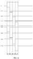
- FIG. 6 which is still another structural diagram of a display panel according to an embodiment of the present disclosure
- the display panel 100 in this embodiment further includes four clock signal line groups, including a first clock signal line group CK 1 , a second clock signal line group CK 2 , a third clock signal line group CK 3 , and a fourth clock signal line group CK 4 .
- Control terminals 1701 of four switch element groups electrically connected to the first data output 191 are electrically connected to the four clock signal line groups in one-to-one correspondence, and control terminals 1701 of four switch element groups electrically connected to the second data output 192 are also electrically connected to the four clock signal line groups in one-to-one correspondence.
- the four switch element groups 170 electrically connected to the first data output 191 transmit data signals to the corresponding four pixel columns
- the four switch element groups 170 electrically connected to the second data output 192 transmit data signals to the corresponding four pixel columns, thereby completing the charging for the first pixel column unit 131 and the second pixel column unit 132 included in one pixel column unit group 13 .
- each row contains N pixel column unit groups
- the connection manner in each pixel column unit group is the same. Therefore, only four clock signal line groups are needed to complete the charging process for a row of pixels, thereby saving charging time for pixels in a same row.
- FIGS. 8-10 of which each is another structural schematic diagram of a display panel according to an embodiment of the present disclosure
- the control terminals 1701 of the four switch element groups 170 corresponding to the four data lines 150 in the first data line unit 151 are electrically connected to the four clock signal line groups in one-to-one correspondence
- the control terminals 1701 of the four switch element groups 170 corresponding to the four data lines 150 in the second data line unit 152 are electrically connected to the four clock signal line groups in one-to-one correspondence.
- the driving method will be described in the following by taking the structure of the display panel and the first color pixels 1011 shown in FIG. 6 as an example.
- FIG. 7 is a sequence diagram of a display panel according to an embodiment of the present disclosure, and in particular a sequence diagram for the first color pixels 1011 shown in FIG. 6 receiving data signals.
- the display panel 100 further includes a plurality of gate lines 23 , and each of the plurality of gate lines 23 is electrically connected to a respective one row of pixels.
- a first row of pixels corresponds to a first gate line 231
- a second row of pixels corresponds to a second gate line 232 .
- the scanning time for every two adjacent gate lines 23 is one cycle G.
- the scanning time for a previous gate line is a first sub-cycle G 1
- the scanning time for the remaining one gate line is a second sub-cycle G 2
- the first sub-cycle G 1 and the second sub-cycle G 2 each includes four time periods, namely t 1 , t 2 , t 3 , and t 4 .
- the driving method for the display panel includes the following steps.
- a data signal is provided to the first data output 191 , and an enable signal is provided to each of the four clock signal line groups.
- a data signal is provided to the second data output 192 , and an enable signal is provided to each of the four clock signal line groups.
- the first clock signal line group CK 1 provides an enable signal to a switch element group 170 corresponding to the third column of pixels 1303 in the first pixel column unit 131 , so that first and second terminals of the switch element group 170 are switched on.
- the second data output 192 since the second data output 192 is not turned on, there is no corresponding signal transmitted to the third color pixel 1013 in the first pixel column unit 131 .
- the first clock signal line group CK 1 provides an enable signal to a switch element group 170 corresponding to the second column of pixels 1302 in the second pixel column unit 132 , so that first and second terminals of the switch element group 170 are switched on.
- the first data output terminal 191 is not turned on, there is no corresponding data signal transmitted to the second color pixel 1012 in the second pixel column unit 132 .
- the second clock signal line group CK 2 is turned on, and the switch element groups 170 electrically connected to the second clock signal line group CK 2 are turned on.
- the second data output 192 since the second data output 192 is not turned on, there is no corresponding signal transmitted to the fourth color pixel 1014 in the first pixel column unit 131 .
- the first data output 191 is turned on, so the data signal with positive polarity can be transmitted to the corresponding first color pixels 1011 in the second pixel column unit 132 .
- the transmission process of the data signal is similar in the third period t 3 and the fourth period t 4 and the second sub-cycle G 2 , and will not be further described herein.
- the polarity of the data signal received by some first color pixels 1011 is positive, and polarity of the data signal received by some other first color pixels 1011 is negative.
- a scanning is performed on each row of gate lines based on the abovementioned manner, except that the polarity of the data signal output from the first data output 191 to the corresponding pixels is negative, and the polarity of the data signal output from the second data output 192 to the corresponding pixels is positive.
- the polarity of the data signal received by some first color pixels 1011 changes from positive to negative, and the polarity of the data signal received by some other first color pixels 1011 changes from negative to positive, so that when switching between two adjacent frames, the polarity of the data signal received by some pixels having a same color changes from positive to negative, and the polarity of the data signal received by some other pixels having the same color changes from negative to positive, thereby effectively alleviating the flickering phenomenon and thus improving the display effect.
- data lines connected to pixels having a same color in a same row are connected to different clock signal line groups.
- switching on is implemented in time division so that pixels having a same color are charged in time division, thus avoiding the mutual interference caused by the simultaneous charging of pixels having a same color and thus improving the display effect.
- the polarity of the data signal provided to the first data output is positive, and in the second sub-cycle, the polarity of the data signal provided to the second data output is negative.
- the polarity of the data signal provided to the first data output is negative
- the polarity of the data signal provided to the second data output is positive
- the first sub-cycle corresponds to a time period of scanning one gate line
- the second sub-cycle corresponds to a time period of scanning another gate line.
- the time required for scanning all gate lines included in the entire display panel can be understood as one frame of time.
- the polarity of the data signal output from the first data output is opposite to the polarity of the data signal output from the second data output, so as to achieve that within the current frame, the polarity of the data signal received by some pixels having a same color is positive and the polarity of the data signal received by some other pixels having the same color is negative, and further in the next frame, the polarity of the data signal received by some pixels having the same color changes from positive to negative and the polarity of the data signal received by some other pixels having the same color changes from negative to positive, thereby avoiding the flickering phenomenon.
- FIG. 11 and FIG. 13 each of which is another structural schematic diagram of a display panel according to an embodiment of the present disclosure.
- the control terminals 1701 of the four switch element groups 170 corresponding to the four data lines 150 in the first data line unit 151 are electrically connected to two clock signal line groups
- the control terminals 1701 of the four switch element groups 170 corresponding to the four data lines 150 in the second data line unit 152 are electrically connected to the other two clock signal line groups.
- the four switch element groups in the driving unit are named as a switch element group 170 A, a switch element group 170 B, a switch element group 170 C, and a switch element group 170 D.
- control terminals 1701 of the switch element group 170 A and the switch element group 170 B are connected to the first clock signal line group CK 1
- control terminals 1701 of the switch element group 170 C and the switch element group 170 D are connected to the second clock signal line group CK 2 .
- control terminals 1701 of the switch element group 170 A and the switch element group 170 B are connected to the third clock signal line group CK 3
- control terminals 1701 of the switch element group 170 C and the switch element group 170 D are connected to the fourth clock signal line group CK 4 .
- FIG. 12 is a time sequence of signals driving a display panel according to an embodiment of the present disclosure, and particularly a sequence diagram for the first color pixels 1011 shown in FIG. 11 receiving data signals.
- the display panel 100 further includes a plurality of gate lines 23 , and each of the plurality of gate lines 23 is electrically connected to a respective one row of pixels.
- a first row of pixels corresponds to a first gate line 231
- a second row of pixels corresponds to a second gate line 232 .
- the scanning time for every two adjacent gate lines 23 is one cycle G.
- the scanning time for a previous gate line is a first sub-cycle G 1
- the scanning time for the remaining one gate line is a second sub-cycle G 2
- the first sub-cycle G 1 and the second sub-cycle G 2 each includes four periods, namely t 1 , t 2 , t 3 , and t 4 .
- the driving method for the display panel includes the following steps.
- a data signal is provided to the first data output 191 , and an enable signal is provided to each of the four clock signal line groups.
- a data signal is provided to the second data output, and an enable signal is provided to each of the four clock signal line groups.
- a data signal is provided to the first data output 191 .
- the first clock signal line group CK 1 When the first clock signal line group CK 1 is turned on, the first clock signal line group CK 1 provides an enable signal to the switch element group 170 A corresponding to the first column of pixels 1301 in the first pixel column unit 131 and the switch element group 170 B corresponding to the second column of pixels 1302 in the first pixel column unit 131 , so that first and second terminals of the switch element group 170 A and the switch element group 170 B are switched on.
- the switch element group 170 A corresponding to the first column of pixels 1301 is electrically connected to the first data output 191
- the second data output 192 electrically connected to the switch element group 170 B corresponding to the second column of pixels 1302 is not turned on, only the data signal having a positive polarity output from the first signal output 191 is transmitted to the first color pixel 1011 .
- the second time signal line group CK 2 is turned on, the first data output 191 and the second data output 192 are not turned on.
- the first clock signal line group CK 1 provides an enable signal so that first and second terminals of the corresponding switch element group are switched on, the first data output 191 and the second data output 192 do not work and no data signal with a positive or negative polarity is output to the corresponding pixels.
- a data signal is provided to the second data output 192 and an enable signal is provided to the second clock signal line group CK 2 , so that the data signal having a negative polarity output from the second data output 192 is transmitted to the corresponding first color pixels 1011 .
- the process in the third period t 3 is similar to that in the first period t 1 and the process in the fourth period t 4 is similar to that in the second period t 2 , and thus no further description will be made herein.
- the scanning manner of gate lines 23 is the same as that in the previous frame, except that the polarity of the data signal output from the first data output 191 changes from positive to negative, and the polarity of the data signal output from the second data output 192 changes from negative to positive.
- the polarity of the data signal received by some first color pixels 1011 changes from positive to negative
- the polarity of the data signal received by other first color pixels 1011 changes from negative to positive, thereby avoiding the flicker phenomenon and thus improving the display quality of the display panel.
- the driving method of the display panel shown in FIG. 13 is similar to the driving method of the display panel shown in FIG. 11 . Only when a data output and a corresponding clock signal line group are both turned on, a data signal having a positive polarity or negative is transmitted to corresponding pixels.
- the polarity of the data signal received by some pixels having a same color is positive, and the polarity of the data signal received by some other pixels having the same color is negative, so that in the polarity inversion process of the next frame, the polarity of the data signal received by some pixels having this color changes from positive to negative and the polarity of the data signal received by some other pixels having this color changes from negative to positive, thereby avoiding the flickering phenomenon.
- each clock signal line group includes a clock signal line. That is, the first clock signal line group CK 1 includes one clock signal line CK 11 , the second clock signal line group CK 2 includes a clock signal line CK 12 , the third clock signal line group CK 3 includes a clock signal line CK 13 , and the fourth clock signal line group CK 4 includes a clock signal line CK 14 .
- Each switch element group 170 includes a switch element 1711 , the control terminals 1701 of the four switch elements 1711 electrically connected to the first data output 191 are electrically connected to four clock signal lines in one-to-one correspondence, and the control terminals 1701 of the four switch elements 1711 electrically connected to the second data output 192 are electrically connected to four clock signal lines in one-to-one correspondence.
- data signals output from the data output may need to be different. Only outputting different data signals according to different colors in time division can achieve the normal display functions, and thus avoid inputting a same data signal to different color pixels at the same time, which may affect the display effect.
- the switch element 1711 in this embodiment can be an N-type thin film transistor or a P-type thin film transistor.
- the abovementioned clock signal line group outputs a high-level signal to control the switch element 1711 to be switched on
- a P-type thin film transistor is used as the switch element 1711
- the abovementioned clock signal line group outputs a low-level signal to control the switch element 1711 to be switched on.
- FIG. 14 exemplifies the switch element 1711 as an N-type thin film transistor.
- each clock signal line group 21 in this embodiment includes two clock signal lines. That is, the first clock signal line group CK 1 includes one clock signal line CK 11 and one clock signal line CK 21 , the second clock signal line group CK 2 includes one clock signal line CK 12 and one clock signal line CK 22 , the third clock signal line group CK 3 includes one clock signal line CK 13 and one clock signal line CK 23 , and the fourth clock signal line group CK 4 includes one clock signal line CK 14 and one clock signal line CK 24 .
- each switch element group 170 includes a first switch element 1721 and a second switch element 1722 .
- the type of the first switch element 1721 is different from the type of the second switch element 1722 .
- the first switch element 1721 can be an N-type thin film transistor
- the second switch element 1722 can be a P-type thin film transistor.
- a switch element group is formed by a P-type thin film transistor and an N-type thin film transistor, so as to overcome the problem that there is a threshold loss when the P-type thin film transistor transmits a low-level signal, there is no threshold loss when the P-type thin film transistor transmits a high-level signal, there is a threshold loss when the N-type thin film transistor transmits a high-level signal and there is no threshold loss when the N-type thin film transistor transmits a low-level signal.
- forming one switch element group by using a P-type thin film transistor and an N-type thin film transistor can achieve that there is no threshold loss no matter transmitting a high-level signal or transmitting a low-level signal.
- FIG. 15 there are various connection manners between each clock signal line group and the switch element groups.
- FIG. 16 is another time sequence of signals driving a display panel according to an embodiment of the present disclosure.
- the driving method for the display panel will be described in the following.
- the first gate line is turned on, i.e., during the first sub-cycle G 1 , in the first period t 1 , the clock signal line CK 11 and the clock signal line CK 21 are turned on, the first terminal and second terminal of the first switch element 1721 electrically connected to the clock signal line CK 11 are switched on, and the first terminal and second terminal of the second switch element 1722 electrically connected to the clock signal line CK 21 are switched on, so that the data signal with positive polarity output from the first data output 191 is transmitted to the corresponding pixels.
- the process in the second period t 2 , the third period t 3 and the fourth period t 4 are similar to that in the abovementioned first period t 1 , and will not be further described herein.
- a time period for scanning all of the i grid lines of the display panel is a frame time. In the current frame, the polarity of the data signal received by some pixels having a same color is positive, and the polarity of the data signal received by some other pixels having the same color is negative.
- the scanning manner is the same as the scanning manner in the previous frame, except that the polarity of the data signal output from the first data output 191 in the previous frame changes from positive to negative and the polarity of the data signal output from the second data output 192 changes from negative to positive.
- the polarity of the data signal received by some pixels having a same color changes from positive to negative
- the polarity of the data signal received by some other pixels having the same color changes from negative to positive, thereby avoiding the flicker phenomenon and thus improving the image quality.
- a first color pixel 1011 and a third color pixel 1013 in the first column of pixels 1301 are repeatedly and alternatively arranged in the column direction
- a second color pixel 1012 and a fourth color pixels 1014 in the second column of pixels 1302 are repeatedly and alternatively arranged in the column direction
- a third color pixels 1013 and a first color pixels 1011 in the third column of pixels 1303 are repeatedly and alternatively arranged in the column direction
- a fourth color pixel 1014 and a second color pixels 1012 in the fourth column of pixels 1304 are repeatedly and alternatively arranged in the column direction.
- colors of the four pixels in a same row are all different from one another; and in the second pixel column unit 132 , colors of the four pixels in a same row are all different from one another. In this way, the uniformity of color mixture of the display panel is improved.
- the first color pixel 1011 can be a red pixel
- the second color pixel 1012 can be a green pixel
- the third color pixel 1013 can be a blue pixel
- the fourth color pixel 1014 can be a white pixel.
- a white pixel with the high light transmittance is selected to increase the overall light transmittance of the display panel.
- power consumption of the display panel can be decreased.
- colors of the four pixels in a same row are all different from one another; and in the second pixel column unit 132 , colors of the four pixels in a same row are all different from one another.
- every two adjacent pixels having a same color in a same row are separated by three pixels of other colors.
- one red pixel closest to one red pixel in a first pixel column unit is located in a second pixel column unit adjacent to this first pixel column unit, and there is a green pixel, a blue pixel, and a white pixel between the two red pixels.
- a red pixel, a green pixel, a blue pixel, and a white pixel are sequentially and cyclically arranged so as to prevent pixels having a same color from being too close to each other in the row direction. This can further improve the uniformity of color mixture in the display panel, and thus improve the display effect.
- an aperture area of the white pixel may be smaller than each of an aperture area of the red pixel, an aperture area of the green pixel, and an aperture area of the blue pixel. Since the light transmittance of the white pixel is higher than the light transmittance of other color pixels, the aperture area of the white pixel can be set to be smaller than the aperture area of other color pixels, so that the light transmittance of a pixel corresponding to each color can be balanced, especially when a solid color image is changed, this can avoid a significant difference in brightness.
- the white pixel since the white pixel has a smaller aperture area, its corresponding charging time is shorter, and the power consumption of the display panel can be decreased.
- the display panel 100 in this embodiment may be a liquid crystal display panel.
- the related description above can be referred for its structure and display principle.
- FIG. 17 is a structural schematic diagram of a display device according to an embodiment of the present disclosure.
- the display device 500 includes a display panel 100 described in the above embodiments.
- FIG. 17 uses a cellphone as an example of a display device.
- the display device is not limited to a cellphone, and can include but is not limited to any electronic device with a display function such as a personal computer (PC), a personal digital assistant (PDA), a wireless handheld device, a tablet computer, an MP4 player, or a television.
- PC personal computer
- PDA personal digital assistant
- the display device 500 in this embodiment includes the display panel described in the above embodiments. Therefore, the display device can also realize all the functions of the above display panel. Similarly, the display device can have the following beneficial effects.
- the data signal received by some pixels having a same color can change from a first signal to a second signal, and the data signal received by other pixels having the same color can change from the second signal to the first signal.
- the polarity of the first signal is opposite to the polarity of the second signal. In this way, when switching between two adjacent frames, it can avoid the flickering phenomenon due to significant non-uniform brightness caused by a polarity of a data signal received by all pixels having a same color changing from one polarity to another polarity for the entire image, thereby improving the display quality.
- the embodiments of the present disclosure can avoid the flickering phenomenon due to the significant non-uniform brightness caused by a polarity of a data signal received by all pixels having a same color changing from one polarity to another polarity for the entire image while switching between two adjacent frames of images, thereby improving the display quality.
- the data signal received by some pixels having a same color changes from a first signal to a second signal
- the data signal received by some other pixels having the same color changes from the second signal to the first signal, thereby avoiding the flickering phenomenon caused by signals received by all pixels having a same color changing from one polarity to another polarity for the entire image.
Landscapes
- Physics & Mathematics (AREA)
- Engineering & Computer Science (AREA)
- General Physics & Mathematics (AREA)
- Crystallography & Structural Chemistry (AREA)
- Chemical & Material Sciences (AREA)
- Nonlinear Science (AREA)
- Theoretical Computer Science (AREA)
- Computer Hardware Design (AREA)
- Mathematical Physics (AREA)
- Optics & Photonics (AREA)
- Microelectronics & Electronic Packaging (AREA)
- Geometry (AREA)
- Control Of Indicators Other Than Cathode Ray Tubes (AREA)
- Liquid Crystal Display Device Control (AREA)
Abstract
Description
Claims (15)
Applications Claiming Priority (3)
| Application Number | Priority Date | Filing Date | Title |
|---|---|---|---|
| CN201810149771 | 2018-02-13 | ||
| CN201810149771.5A CN108333841B (en) | 2018-02-13 | 2018-02-13 | Display panel, display device and driving method thereof |
| CN201810149771.5 | 2018-02-13 |
Publications (2)
| Publication Number | Publication Date |
|---|---|
| US20190251918A1 US20190251918A1 (en) | 2019-08-15 |
| US10692450B2 true US10692450B2 (en) | 2020-06-23 |
Family
ID=62929562
Family Applications (1)
| Application Number | Title | Priority Date | Filing Date |
|---|---|---|---|
| US15/994,937 Active 2038-09-04 US10692450B2 (en) | 2018-02-13 | 2018-05-31 | Display panel, display device, and driving method |
Country Status (2)
| Country | Link |
|---|---|
| US (1) | US10692450B2 (en) |
| CN (1) | CN108333841B (en) |
Families Citing this family (6)
| Publication number | Priority date | Publication date | Assignee | Title |
|---|---|---|---|---|
| CN109887459A (en) * | 2019-04-24 | 2019-06-14 | 厦门天马微电子有限公司 | Driving method, driving circuit and the display device of display panel |
| CN110441969A (en) * | 2019-08-20 | 2019-11-12 | 京东方科技集团股份有限公司 | A display substrate, its driving method and display device |
| US11189241B2 (en) * | 2020-03-27 | 2021-11-30 | Tcl China Star Optoelectronics Technology Co., Ltd | Method for charging pixels and display panel |
| CN111766746B (en) * | 2020-06-24 | 2022-06-03 | 厦门天马微电子有限公司 | Display panel, driving method thereof and display device |
| CN115315742B (en) * | 2021-03-04 | 2025-04-11 | 京东方科技集团股份有限公司 | Light-emitting substrate, display device, and method for driving the light-emitting substrate |
| CN113674672B (en) * | 2021-08-18 | 2023-06-27 | 深圳市华星光电半导体显示技术有限公司 | Display panel driving method and display panel |
Citations (17)
| Publication number | Priority date | Publication date | Assignee | Title |
|---|---|---|---|---|
| US20070040764A1 (en) * | 2005-08-17 | 2007-02-22 | Yang-Wan Kim | Data driver and organic light emitting display having the same |
| US20080278466A1 (en) * | 2007-05-11 | 2008-11-13 | Samsung Electronics Co., Ltd. | Liquid crystal display and method of driving the same |
| US7505053B2 (en) * | 2004-04-09 | 2009-03-17 | Samsung Electronics Co., Ltd. | Subpixel layouts and arrangements for high brightness displays |
| US20110249046A1 (en) * | 2010-04-07 | 2011-10-13 | Samsung Mobile Display Co., Ltd. | Liquid crystal display device |
| US20110299023A1 (en) * | 2003-04-17 | 2011-12-08 | Lee Baek-Woon | Liquid crystal display |
| US8199102B2 (en) * | 2007-05-18 | 2012-06-12 | Samsung Electronics Co., Ltd. | Liquid crystal display and method of driving the same utilizing data line blocks |
| CN103996383A (en) | 2013-02-18 | 2014-08-20 | 三星显示有限公司 | Display device |
| US9129569B2 (en) * | 2010-02-26 | 2015-09-08 | Sharp Kabushiki Kaisha | Liquid crystal display device |
| US9224348B2 (en) * | 2010-07-27 | 2015-12-29 | Lg Display Co., Ltd. | Liquid crystal display |
| CN105405416A (en) | 2014-09-05 | 2016-03-16 | 三星显示有限公司 | Display apparatus and method of driving the same |
| US9437153B2 (en) * | 2013-01-10 | 2016-09-06 | Japan Display Inc. | Liquid crystal display device |
| CN106292086A (en) | 2016-09-06 | 2017-01-04 | 武汉华星光电技术有限公司 | A kind of liquid crystal panel based on four color technology |
| US9589515B2 (en) * | 2013-07-12 | 2017-03-07 | Shanghai Tianma Micro-electronics Co., Ltd. | Display panel and display device |
| US20180047353A1 (en) * | 2016-01-04 | 2018-02-15 | Wuhan China Star Optoelectronics Technology Co., Ltd. | Demultiplex type display driving circuit |
| US9952474B2 (en) * | 2014-09-05 | 2018-04-24 | Shenzhen China Star Optoelectronics Technology Co., Ltd. | Deskew display panel comprising a plurality of scanning lines taking a periodic ladder shape |
| US20180356676A1 (en) * | 2017-06-08 | 2018-12-13 | HKC Corporation Limited | Pixel structure and display panel having the same |
| US10510315B2 (en) * | 2018-01-30 | 2019-12-17 | Xiamen Tianma Micro-Electronics Co., Ltd. | Display panel, driving method thereof and display device |
Family Cites Families (4)
| Publication number | Priority date | Publication date | Assignee | Title |
|---|---|---|---|---|
| KR101429905B1 (en) * | 2006-09-29 | 2014-08-14 | 엘지디스플레이 주식회사 | Liquid crystal display |
| JP5216204B2 (en) * | 2006-10-31 | 2013-06-19 | 株式会社半導体エネルギー研究所 | Liquid crystal display device and manufacturing method thereof |
| CN101221716B (en) * | 2008-01-24 | 2010-06-02 | 友达光电股份有限公司 | Data driver using gamma selection signal, flat panel display and driving method thereof |
| CN106991925A (en) * | 2017-06-08 | 2017-07-28 | 惠科股份有限公司 | Pixel structure and display panel thereof |
-
2018
- 2018-02-13 CN CN201810149771.5A patent/CN108333841B/en active Active
- 2018-05-31 US US15/994,937 patent/US10692450B2/en active Active
Patent Citations (20)
| Publication number | Priority date | Publication date | Assignee | Title |
|---|---|---|---|---|
| US20110299023A1 (en) * | 2003-04-17 | 2011-12-08 | Lee Baek-Woon | Liquid crystal display |
| US7505053B2 (en) * | 2004-04-09 | 2009-03-17 | Samsung Electronics Co., Ltd. | Subpixel layouts and arrangements for high brightness displays |
| US20070040764A1 (en) * | 2005-08-17 | 2007-02-22 | Yang-Wan Kim | Data driver and organic light emitting display having the same |
| US20080278466A1 (en) * | 2007-05-11 | 2008-11-13 | Samsung Electronics Co., Ltd. | Liquid crystal display and method of driving the same |
| US8199102B2 (en) * | 2007-05-18 | 2012-06-12 | Samsung Electronics Co., Ltd. | Liquid crystal display and method of driving the same utilizing data line blocks |
| US9129569B2 (en) * | 2010-02-26 | 2015-09-08 | Sharp Kabushiki Kaisha | Liquid crystal display device |
| US20110249046A1 (en) * | 2010-04-07 | 2011-10-13 | Samsung Mobile Display Co., Ltd. | Liquid crystal display device |
| US9224348B2 (en) * | 2010-07-27 | 2015-12-29 | Lg Display Co., Ltd. | Liquid crystal display |
| US9437153B2 (en) * | 2013-01-10 | 2016-09-06 | Japan Display Inc. | Liquid crystal display device |
| US20140232624A1 (en) * | 2013-02-18 | 2014-08-21 | Samsung Display Co., Ltd. | Display device |
| CN103996383A (en) | 2013-02-18 | 2014-08-20 | 三星显示有限公司 | Display device |
| US9715861B2 (en) * | 2013-02-18 | 2017-07-25 | Samsung Display Co., Ltd | Display device having unit pixel defined by even number of adjacent sub-pixels |
| US9589515B2 (en) * | 2013-07-12 | 2017-03-07 | Shanghai Tianma Micro-electronics Co., Ltd. | Display panel and display device |
| CN105405416A (en) | 2014-09-05 | 2016-03-16 | 三星显示有限公司 | Display apparatus and method of driving the same |
| US9952474B2 (en) * | 2014-09-05 | 2018-04-24 | Shenzhen China Star Optoelectronics Technology Co., Ltd. | Deskew display panel comprising a plurality of scanning lines taking a periodic ladder shape |
| US20180047353A1 (en) * | 2016-01-04 | 2018-02-15 | Wuhan China Star Optoelectronics Technology Co., Ltd. | Demultiplex type display driving circuit |
| US10049638B2 (en) * | 2016-01-04 | 2018-08-14 | Wuhan China Star Optoelectronics Technology Co., Ltd. | Demultiplex type display driving circuit |
| CN106292086A (en) | 2016-09-06 | 2017-01-04 | 武汉华星光电技术有限公司 | A kind of liquid crystal panel based on four color technology |
| US20180356676A1 (en) * | 2017-06-08 | 2018-12-13 | HKC Corporation Limited | Pixel structure and display panel having the same |
| US10510315B2 (en) * | 2018-01-30 | 2019-12-17 | Xiamen Tianma Micro-Electronics Co., Ltd. | Display panel, driving method thereof and display device |
Also Published As
| Publication number | Publication date |
|---|---|
| CN108333841A (en) | 2018-07-27 |
| CN108333841B (en) | 2021-04-09 |
| US20190251918A1 (en) | 2019-08-15 |
Similar Documents
| Publication | Publication Date | Title |
|---|---|---|
| US10692450B2 (en) | Display panel, display device, and driving method | |
| CN108231031B (en) | Display panel, driving method thereof and display device | |
| US11475857B2 (en) | Array substrate and display device | |
| US10176772B2 (en) | Display device having an array substrate | |
| CN104751821B (en) | Display panel and its driving method | |
| US12021088B2 (en) | Array substrate, display apparatus and drive method therefor | |
| US10192510B2 (en) | Source driving module generating two groups of gamma voltages and liquid crystal display device using same | |
| US11527213B2 (en) | Driving method of display panel for reducing viewing angle color deviation and display device | |
| US10535321B2 (en) | Display panel, display device and driving method of display panel | |
| US20170032749A1 (en) | Liquid crystal display device | |
| US10971091B2 (en) | Array substrate, display panel and driving method thereof, and display device | |
| US9766495B2 (en) | Transflective type liquid crystal panel | |
| CN106340279B (en) | Driving method, drive device and the display device of display panel | |
| CN111223463A (en) | Display panel, driving method thereof and display device | |
| CN114999418A (en) | Liquid crystal display module, driving method thereof and liquid crystal display device | |
| CN108198539A (en) | Display panel and its driving method, display device | |
| CN116631354A (en) | Array substrate and driving method thereof | |
| US9460672B2 (en) | Method for driving a liquid crystal display panel and liquid crystal display | |
| CN113270076A (en) | Display panel driving method and display device | |
| US12205511B2 (en) | Display panel, driving method thereof, and electronic device | |
| US12562133B2 (en) | Display device and driving method thereof | |
| US10360869B2 (en) | Liquid crystal panel driving circuit and liquid crystal display device | |
| US20240249693A1 (en) | Drive method for display panel, and display apparatus | |
| CN113439297B (en) | Display device and driving method thereof | |
| US10796651B2 (en) | Driving method and device of display panel, and display device |
Legal Events
| Date | Code | Title | Description |
|---|---|---|---|
| FEPP | Fee payment procedure |
Free format text: ENTITY STATUS SET TO UNDISCOUNTED (ORIGINAL EVENT CODE: BIG.); ENTITY STATUS OF PATENT OWNER: LARGE ENTITY |
|
| AS | Assignment |
Owner name: XIAMEN TIANMA MICRO-ELECTRONICS CO.,LTD, CHINA Free format text: ASSIGNMENT OF ASSIGNORS INTEREST;ASSIGNORS:WANG, JIANXUN;ZHOU, HONGBO;YANG, WENBIN;REEL/FRAME:046290/0244 Effective date: 20180522 |
|
| STPP | Information on status: patent application and granting procedure in general |
Free format text: NON FINAL ACTION MAILED |
|
| STPP | Information on status: patent application and granting procedure in general |
Free format text: RESPONSE TO NON-FINAL OFFICE ACTION ENTERED AND FORWARDED TO EXAMINER |
|
| STPP | Information on status: patent application and granting procedure in general |
Free format text: NOTICE OF ALLOWANCE MAILED -- APPLICATION RECEIVED IN OFFICE OF PUBLICATIONS |
|
| STPP | Information on status: patent application and granting procedure in general |
Free format text: PUBLICATIONS -- ISSUE FEE PAYMENT VERIFIED |
|
| STCF | Information on status: patent grant |
Free format text: PATENTED CASE |
|
| MAFP | Maintenance fee payment |
Free format text: PAYMENT OF MAINTENANCE FEE, 4TH YEAR, LARGE ENTITY (ORIGINAL EVENT CODE: M1551); ENTITY STATUS OF PATENT OWNER: LARGE ENTITY Year of fee payment: 4 |