US10692445B2 - Method for driving display apparatus with a plurality of gamma grayscale value curve alternately - Google Patents
Method for driving display apparatus with a plurality of gamma grayscale value curve alternately Download PDFInfo
- Publication number
- US10692445B2 US10692445B2 US16/068,397 US201816068397A US10692445B2 US 10692445 B2 US10692445 B2 US 10692445B2 US 201816068397 A US201816068397 A US 201816068397A US 10692445 B2 US10692445 B2 US 10692445B2
- Authority
- US
- United States
- Prior art keywords
- grayscale value
- gamma
- curve
- value corresponding
- display apparatus
- Prior art date
- Legal status (The legal status is an assumption and is not a legal conclusion. Google has not performed a legal analysis and makes no representation as to the accuracy of the status listed.)
- Active
Links
Images


Classifications
-
- G—PHYSICS
- G09—EDUCATION; CRYPTOGRAPHY; DISPLAY; ADVERTISING; SEALS
- G09G—ARRANGEMENTS OR CIRCUITS FOR CONTROL OF INDICATING DEVICES USING STATIC MEANS TO PRESENT VARIABLE INFORMATION
- G09G3/00—Control arrangements or circuits, of interest only in connection with visual indicators other than cathode-ray tubes
- G09G3/20—Control arrangements or circuits, of interest only in connection with visual indicators other than cathode-ray tubes for presentation of an assembly of a number of characters, e.g. a page, by composing the assembly by combination of individual elements arranged in a matrix no fixed position being assigned to or needed to be assigned to the individual characters or partial characters
- G09G3/34—Control arrangements or circuits, of interest only in connection with visual indicators other than cathode-ray tubes for presentation of an assembly of a number of characters, e.g. a page, by composing the assembly by combination of individual elements arranged in a matrix no fixed position being assigned to or needed to be assigned to the individual characters or partial characters by control of light from an independent source
- G09G3/36—Control arrangements or circuits, of interest only in connection with visual indicators other than cathode-ray tubes for presentation of an assembly of a number of characters, e.g. a page, by composing the assembly by combination of individual elements arranged in a matrix no fixed position being assigned to or needed to be assigned to the individual characters or partial characters by control of light from an independent source using liquid crystals
- G09G3/3607—Control arrangements or circuits, of interest only in connection with visual indicators other than cathode-ray tubes for presentation of an assembly of a number of characters, e.g. a page, by composing the assembly by combination of individual elements arranged in a matrix no fixed position being assigned to or needed to be assigned to the individual characters or partial characters by control of light from an independent source using liquid crystals for displaying colours or for displaying grey scales with a specific pixel layout, e.g. using sub-pixels
-
- G—PHYSICS
- G09—EDUCATION; CRYPTOGRAPHY; DISPLAY; ADVERTISING; SEALS
- G09G—ARRANGEMENTS OR CIRCUITS FOR CONTROL OF INDICATING DEVICES USING STATIC MEANS TO PRESENT VARIABLE INFORMATION
- G09G3/00—Control arrangements or circuits, of interest only in connection with visual indicators other than cathode-ray tubes
- G09G3/20—Control arrangements or circuits, of interest only in connection with visual indicators other than cathode-ray tubes for presentation of an assembly of a number of characters, e.g. a page, by composing the assembly by combination of individual elements arranged in a matrix no fixed position being assigned to or needed to be assigned to the individual characters or partial characters
- G09G3/34—Control arrangements or circuits, of interest only in connection with visual indicators other than cathode-ray tubes for presentation of an assembly of a number of characters, e.g. a page, by composing the assembly by combination of individual elements arranged in a matrix no fixed position being assigned to or needed to be assigned to the individual characters or partial characters by control of light from an independent source
- G09G3/36—Control arrangements or circuits, of interest only in connection with visual indicators other than cathode-ray tubes for presentation of an assembly of a number of characters, e.g. a page, by composing the assembly by combination of individual elements arranged in a matrix no fixed position being assigned to or needed to be assigned to the individual characters or partial characters by control of light from an independent source using liquid crystals
- G09G3/3611—Control of matrices with row and column drivers
- G09G3/3674—Details of drivers for scan electrodes
- G09G3/3677—Details of drivers for scan electrodes suitable for active matrices only
-
- G—PHYSICS
- G02—OPTICS
- G02F—OPTICAL DEVICES OR ARRANGEMENTS FOR THE CONTROL OF LIGHT BY MODIFICATION OF THE OPTICAL PROPERTIES OF THE MEDIA OF THE ELEMENTS INVOLVED THEREIN; NON-LINEAR OPTICS; FREQUENCY-CHANGING OF LIGHT; OPTICAL LOGIC ELEMENTS; OPTICAL ANALOGUE/DIGITAL CONVERTERS
- G02F1/00—Devices or arrangements for the control of the intensity, colour, phase, polarisation or direction of light arriving from an independent light source, e.g. switching, gating or modulating; Non-linear optics
- G02F1/01—Devices or arrangements for the control of the intensity, colour, phase, polarisation or direction of light arriving from an independent light source, e.g. switching, gating or modulating; Non-linear optics for the control of the intensity, phase, polarisation or colour
- G02F1/13—Devices or arrangements for the control of the intensity, colour, phase, polarisation or direction of light arriving from an independent light source, e.g. switching, gating or modulating; Non-linear optics for the control of the intensity, phase, polarisation or colour based on liquid crystals, e.g. single liquid crystal display cells
- G02F1/133—Constructional arrangements; Operation of liquid crystal cells; Circuit arrangements
- G02F1/136—Liquid crystal cells structurally associated with a semi-conducting layer or substrate, e.g. cells forming part of an integrated circuit
- G02F1/1362—Active matrix addressed cells
- G02F1/1368—Active matrix addressed cells in which the switching element is a three-electrode device
-
- G—PHYSICS
- G09—EDUCATION; CRYPTOGRAPHY; DISPLAY; ADVERTISING; SEALS
- G09G—ARRANGEMENTS OR CIRCUITS FOR CONTROL OF INDICATING DEVICES USING STATIC MEANS TO PRESENT VARIABLE INFORMATION
- G09G3/00—Control arrangements or circuits, of interest only in connection with visual indicators other than cathode-ray tubes
- G09G3/20—Control arrangements or circuits, of interest only in connection with visual indicators other than cathode-ray tubes for presentation of an assembly of a number of characters, e.g. a page, by composing the assembly by combination of individual elements arranged in a matrix no fixed position being assigned to or needed to be assigned to the individual characters or partial characters
- G09G3/34—Control arrangements or circuits, of interest only in connection with visual indicators other than cathode-ray tubes for presentation of an assembly of a number of characters, e.g. a page, by composing the assembly by combination of individual elements arranged in a matrix no fixed position being assigned to or needed to be assigned to the individual characters or partial characters by control of light from an independent source
- G09G3/36—Control arrangements or circuits, of interest only in connection with visual indicators other than cathode-ray tubes for presentation of an assembly of a number of characters, e.g. a page, by composing the assembly by combination of individual elements arranged in a matrix no fixed position being assigned to or needed to be assigned to the individual characters or partial characters by control of light from an independent source using liquid crystals
- G09G3/3611—Control of matrices with row and column drivers
- G09G3/3685—Details of drivers for data electrodes
- G09G3/3688—Details of drivers for data electrodes suitable for active matrices only
-
- G—PHYSICS
- G02—OPTICS
- G02F—OPTICAL DEVICES OR ARRANGEMENTS FOR THE CONTROL OF LIGHT BY MODIFICATION OF THE OPTICAL PROPERTIES OF THE MEDIA OF THE ELEMENTS INVOLVED THEREIN; NON-LINEAR OPTICS; FREQUENCY-CHANGING OF LIGHT; OPTICAL LOGIC ELEMENTS; OPTICAL ANALOGUE/DIGITAL CONVERTERS
- G02F1/00—Devices or arrangements for the control of the intensity, colour, phase, polarisation or direction of light arriving from an independent light source, e.g. switching, gating or modulating; Non-linear optics
- G02F1/01—Devices or arrangements for the control of the intensity, colour, phase, polarisation or direction of light arriving from an independent light source, e.g. switching, gating or modulating; Non-linear optics for the control of the intensity, phase, polarisation or colour
- G02F1/13—Devices or arrangements for the control of the intensity, colour, phase, polarisation or direction of light arriving from an independent light source, e.g. switching, gating or modulating; Non-linear optics for the control of the intensity, phase, polarisation or colour based on liquid crystals, e.g. single liquid crystal display cells
- G02F1/133—Constructional arrangements; Operation of liquid crystal cells; Circuit arrangements
- G02F1/1333—Constructional arrangements; Manufacturing methods
- G02F1/1343—Electrodes
- G02F1/134309—Electrodes characterised by their geometrical arrangement
- G02F1/134345—Subdivided pixels, e.g. for grey scale or redundancy
-
- G—PHYSICS
- G02—OPTICS
- G02F—OPTICAL DEVICES OR ARRANGEMENTS FOR THE CONTROL OF LIGHT BY MODIFICATION OF THE OPTICAL PROPERTIES OF THE MEDIA OF THE ELEMENTS INVOLVED THEREIN; NON-LINEAR OPTICS; FREQUENCY-CHANGING OF LIGHT; OPTICAL LOGIC ELEMENTS; OPTICAL ANALOGUE/DIGITAL CONVERTERS
- G02F2201/00—Constructional arrangements not provided for in groups G02F1/00 - G02F7/00
- G02F2201/52—RGB geometrical arrangements
-
- G—PHYSICS
- G09—EDUCATION; CRYPTOGRAPHY; DISPLAY; ADVERTISING; SEALS
- G09G—ARRANGEMENTS OR CIRCUITS FOR CONTROL OF INDICATING DEVICES USING STATIC MEANS TO PRESENT VARIABLE INFORMATION
- G09G2300/00—Aspects of the constitution of display devices
- G09G2300/04—Structural and physical details of display devices
- G09G2300/0439—Pixel structures
- G09G2300/0452—Details of colour pixel setup, e.g. pixel composed of a red, a blue and two green components
-
- G—PHYSICS
- G09—EDUCATION; CRYPTOGRAPHY; DISPLAY; ADVERTISING; SEALS
- G09G—ARRANGEMENTS OR CIRCUITS FOR CONTROL OF INDICATING DEVICES USING STATIC MEANS TO PRESENT VARIABLE INFORMATION
- G09G2310/00—Command of the display device
- G09G2310/02—Addressing, scanning or driving the display screen or processing steps related thereto
- G09G2310/0264—Details of driving circuits
- G09G2310/027—Details of drivers for data electrodes, the drivers handling digital grey scale data, e.g. use of D/A converters
-
- G—PHYSICS
- G09—EDUCATION; CRYPTOGRAPHY; DISPLAY; ADVERTISING; SEALS
- G09G—ARRANGEMENTS OR CIRCUITS FOR CONTROL OF INDICATING DEVICES USING STATIC MEANS TO PRESENT VARIABLE INFORMATION
- G09G2320/00—Control of display operating conditions
- G09G2320/02—Improving the quality of display appearance
- G09G2320/0271—Adjustment of the gradation levels within the range of the gradation scale, e.g. by redistribution or clipping
- G09G2320/0276—Adjustment of the gradation levels within the range of the gradation scale, e.g. by redistribution or clipping for the purpose of adaptation to the characteristics of a display device, i.e. gamma correction
-
- G—PHYSICS
- G09—EDUCATION; CRYPTOGRAPHY; DISPLAY; ADVERTISING; SEALS
- G09G—ARRANGEMENTS OR CIRCUITS FOR CONTROL OF INDICATING DEVICES USING STATIC MEANS TO PRESENT VARIABLE INFORMATION
- G09G2320/00—Control of display operating conditions
- G09G2320/06—Adjustment of display parameters
- G09G2320/0673—Adjustment of display parameters for control of gamma adjustment, e.g. selecting another gamma curve
Definitions
- This application relates to a method for designing a display panel, and in particular, to a method for driving a display apparatus and a display apparatus.
- a liquid crystal display panel generally includes a color filter (CF) substrate, a thin film transistor array substrate (TFT Array Substrate), and a liquid crystal layer that is disposed between the two substrates. Its operating principle is to control, by applying a drive voltage to two glass substrates, a liquid crystal molecule on a liquid crystal layer to rotate, and refract light of a backlight module to generate an image.
- CF color filter
- TFT Array Substrate thin film transistor array substrate
- FFS fringe field switching
- Liquid crystal displays of a VA mode include, for example, a patterned vertical alignment (PVA) liquid crystal display or a multi-domain vertical alignment (MVA) liquid crystal display.
- PVA patterned vertical alignment
- MVA multi-domain vertical alignment
- the PVA display achieves a wide viewing angle effect by using a fringing field effect and a compensation plate.
- the MVA display divides one pixel into a plurality of areas, and makes, by using a protrusion or a particular pattern structure, liquid crystal molecules in different areas tilt towards different directions, to achieve a wide viewing angle and improve a penetration transmittance.
- liquid crystal displays are most widely used displays in markets, and in particular, widely used in liquid crystal televisions.
- resolution gradually increases, a size of a pixel is becoming smaller, an aperture ratio is also becoming smaller.
- a color cast phenomenon exists for a large viewing angle.
- a viewing angle problem of a VA display panel becomes a main obstacle that impedes a high resolution of the VA panel, because in a case of high resolution panel design, a penetration transmittance and a viewing angle are factors restricting each other, and consideration can be given to only either of the two but not both.
- a penetration transmittance is 3.7%, and the viewing angle meets a requirement of a customer for 60 degrees on the left and right; if a conventional low color cast is not made, a penetration transmittance is already 5.1%, but the viewing angle cannot meet a requirement for 60 degrees on the left and right.
- an objective of this application is to provide a method for designing a display panel, and in particular, relate to a method for driving a display apparatus and a display apparatus to which the method is applied, so that not only a color cast problem can be effectively resolved, but also a viewing angle of a high resolution large-sized product can be effectively improved.
- a method for driving a display apparatus includes: outputting an output image corresponding to a pixel signal; performing a corresponding grayscale value conversion processing on a pixel grayscale value of the output image; and converting, according to a gamma correction curve, the pixel grayscale value of the output image after the corresponding grayscale value conversion processing into a corresponding applied voltage, and scanning and outputting the corresponding applied voltage to a display panel, wherein the corresponding grayscale value conversion processing splits a gamma standard curve into a first gamma grayscale value corresponding curve and a second gamma grayscale value corresponding curve, and outputs the first gamma grayscale value corresponding curve and the second gamma grayscale value corresponding curve to the output image in an alternate manner, where the output image is processed by using a grayscale value corresponding curve.
- Another objective of this application is a method for driving a display apparatus, including: splitting a gamma standard curve into a first gamma grayscale value corresponding curve and a second gamma grayscale value corresponding curve; obtaining a pixel output signal corresponding result by using the first gamma grayscale value corresponding curve and the second gamma grayscale value corresponding curve; and deciding and controlling, according to the pixel output signal corresponding result, whether a plurality of drive circuit components enters a signal mode, where these drive circuit components include a plurality of first drive chips, a plurality of second drive chips, a power supply control chip, a brightness detector, and a digital-to-analog converter, and the signal mode means outputting grayscale value image data, where the grayscale value image data that is outputted is processed by using a grayscale value corresponding curve.
- Still another objective of this application is a display apparatus, including: a first substrate; a second substrate, disposed opposite to the first substrate; and a drive circuit component, including a plurality of first drive chips, a plurality of second drive chips, a power supply control chip, a brightness detector, and a digital-to-analog converter, where the drive circuit component is disposed on the first substrate or the second substrate.
- an energy required by the first gamma grayscale value corresponding curve and an energy required by the second gamma grayscale value corresponding curve are equal to an energy of a gamma standard curve.
- At least either of the first or second gamma grayscale value corresponding curve is adjustable.
- the gamma correction curve is adjustable.
- a manner of the scanning is fully scanning and outputting an output image, and then fully scanning and outputting a next output image.
- the display apparatus further includes a brightness detector, configured to detect a color luminance of the display panel.
- the display apparatus further includes a digital-to-analog converter, configured to convert red, green, and blue digital signals into analog signals, and input the analog signals into pixel components of corresponding colors by using signal lines on the display panel.
- a digital-to-analog converter configured to convert red, green, and blue digital signals into analog signals, and input the analog signals into pixel components of corresponding colors by using signal lines on the display panel.
- FIG. 1 is a diagram of an exemplary liquid crystal pixel circuit for which a color cast problem is resolved
- FIG. 2 is a schematic diagram of an exemplary area including main pixels and sub pixels;
- FIG. 3 is a schematic diagram of a gamma curve according to an embodiment of this application.
- FIG. 4 is a schematic diagram of a grayscale value curve according to an embodiment of this application.
- FIG. 5 is a flowchart of a method for driving a display apparatus according to an embodiment of this application.
- FIG. 6 is a flowchart of a method for driving a display apparatus according to another embodiment of this application.
- FIG. 7 is a module diagram if a display apparatus according to an embodiment of this application.
- the word “include” is understood as including the component, but not excluding any other component.
- “on” means that one is located above or below a target component and does not necessarily mean that one is located on the top based on a gravity direction.
- a display panel in this application may include a liquid crystal display (LCD) panel, including a thin film transistor (TFT) array substrate, a color filter (CF) substrate, and a liquid crystal layer formed between the two substrates, or is an organic light-emitting diode (OLED) panel or a quantum dots light-emitting diode (QLED) panel.
- LCD liquid crystal display
- TFT thin film transistor
- CF color filter
- OLED organic light-emitting diode
- QLED quantum dots light-emitting diode
- the display panel in this application may be a curved-surface display panel.
- a TFT array and the CF in this application may be formed on a same substrate.
- FIG. 1 is a diagram of an exemplary liquid crystal pixel circuit for which a color cast problem is resolved.
- a liquid crystal display enabling a plurality of capacitors in a pixel to share electric charge with each other is a technology derived for resolving a color cast problem.
- FIG. 1 in the liquid crystal pixel circuit shown in FIG.
- a main pixel is controlled by a scanning line G 1 , to use a transistor T 1 to obtain data from a data line D 1 and store the data to a storage capacitor Cst 1 ; and besides being controlled by the scanning line G 1 , to use a transistor T 2 to obtain data from the data line D 1 and store the data to a storage capacitor Cst 2 , a sub pixel is further controlled by a scanning line G 2 , to use a transistor T 3 to enable the storage capacitor Cst 2 and a storage capacitor Cst 3 to share electric charge with each other.
- a liquid crystal display is improved in terms of both resolution and image update frequency.
- the storage capacitors Cst 1 and Cst 2 may not be fully charged, and consequently the storage voltages of the storage capacitors Cst 1 and Cst 2 may not reach a same level.
- the storage voltages of the storage capacitors Cst 1 and Cst 2 are different, after the storage capacitor Cst 2 and the storage capacitor Cst 3 share electric charge with each other, a ratio of a voltage maintained by the storage capacitor Cst 2 to a voltage maintained by the storage capacitor Cst 1 cannot reach an originally specified ratio. Therefore, the color cast problem that is originally wanted to be eliminated occurs during a display process again.
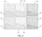
- FIG. 2 is a schematic diagram of an exemplary area including main pixels and sub pixels.
- an area including main pixels and sub pixels including: a main pixel 210 area and a sub pixel 212 area including red pixels, a main pixel 220 area and a sub pixel 222 area including green pixels, and a main pixel 230 area and a sub pixel 232 area including blue pixels.
- FIG. 3 is a schematic diagram of a gamma curve according to an embodiment of this application.
- FIG. 4 is a schematic diagram of a grayscale value curve according to an embodiment of this application.
- a method for driving a gamma curve of a display device includes: outputting an output image corresponding to a pixel signal; performing a corresponding grayscale value conversion processing on a pixel grayscale value of the output image; and converting, according to a gamma correction curve 100 , the pixel grayscale value of the output image after the corresponding grayscale value conversion processing into a corresponding applied voltage, and scanning and outputting the corresponding applied voltage to a display panel, wherein the corresponding grayscale value conversion processing splits a gamma standard curve into a first gamma grayscale value corresponding curve 110 and a second gamma grayscale value corresponding curve 120 , and outputs the first gamma grayscale value corresponding curve 110 and the second gamma grayscale value corresponding
- an energy required by the first gamma grayscale value corresponding curve and an energy required by the second gamma grayscale value corresponding curve are equal to an energy of a gamma standard curve.
- At least either of the first or second gamma grayscale value corresponding curve is adjustable.
- the gamma correction curve is adjustable.
- a manner of the scanning is fully scanning and outputting the output image, and then fully scanning and outputting next output image.
- the display apparatus further includes a brightness detector, configured to detect a color luminance of the display panel.
- the display apparatus further includes a digital-to-analog converter, configured to convert red, green, and blue digital signals into analog signals, and input the analog signals into pixel components of corresponding colors by using signal lines on the display panel.
- a digital-to-analog converter configured to convert red, green, and blue digital signals into analog signals, and input the analog signals into pixel components of corresponding colors by using signal lines on the display panel.
- a method for driving a display apparatus includes: splitting a gamma standard curve 100 into a first gamma grayscale value corresponding curve 110 and a second gamma grayscale value corresponding curve 120 ; obtaining a pixel output signal corresponding result by using the first gamma grayscale value corresponding curve 110 and the second gamma grayscale value corresponding curve 120 ; and deciding and controlling, according to the pixel output signal corresponding result, whether a plurality of drive circuit components enters a signal mode, where these drive circuit components include a plurality of first drive chips, a plurality of second drive chips, a power supply control chip, a brightness detector, and a digital-to-analog converter, and the signal mode means outputting grayscale value image data, where the grayscale value image data that is outputted is processed by using a grayscale value corresponding curve.
- the method for driving a display apparatus further includes a display panel, configured to display an image.
- FIG. 5 is a flowchart of a method for driving a display apparatus according to an embodiment of this application.
- FIG. 6 is a flowchart of a method for driving a display apparatus according to another embodiment of this application. Referring to FIG. 5 , in step S 510 , a pixel signal is outputted from a corresponding output image.
- step S 520 the corresponding grayscale value conversion processing is performed on a pixel grayscale value of the output image.
- step S 530 the output image on which the corresponding grayscale value conversion processing has been performed and the pixel grayscale value on which the corresponding grayscale value conversion processing has been performed are converted into a corresponding applied voltage according to a gamma correction curve, and the corresponding applied voltage is scanned and outputted to a display panel.
- step S 540 the corresponding grayscale value conversion processing splits a gamma standard curve into a first gamma grayscale value corresponding curve and a second gamma grayscale value corresponding curve, and outputs the two curves to the output image in an alternate manner.
- a gamma standard curve is split into a first gamma grayscale value corresponding curve and a second gamma grayscale value corresponding curve.
- step S 620 a pixel output signal corresponding result is obtained by using the first gamma grayscale value corresponding curve and the second gamma grayscale value corresponding curve.
- step S 630 it is decided and controlled, according to the pixel output signal corresponding result, whether a plurality of drive circuit components enters a signal mode.
- these drive circuit components include a plurality of first drive chips, a plurality of second drive chips, a power supply control chip, a brightness detector, and a digital-to-analog converter, and the signal mode means outputting grayscale value image data.
- a method for driving a display panel includes the method for driving a display apparatus.
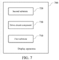
- FIG. 7 is a module diagram if a display apparatus according to an embodiment of this application.
- a display apparatus 700 includes: a first substrate 710 ; a second substrate 720 , disposed opposite to the first substrate 710 ; and a drive circuit component 730 , further including a plurality of first drive chips, a plurality of second drive chips, a power supply control chip, a brightness detector, and a digital-to-analog converter, where the drive circuit component 730 is disposed on the first substrate 710 or the second substrate 720 .
- phrases such as “in some embodiments” and “in various embodiments” are repeatedly used.
- the wordings usually refer to different embodiments, but they may also refer to a same embodiment.
- Words, such as “include”, “have”, and “include” are synonyms, unless other meanings are indicated in the context.
Landscapes
- Engineering & Computer Science (AREA)
- Physics & Mathematics (AREA)
- General Physics & Mathematics (AREA)
- Crystallography & Structural Chemistry (AREA)
- Chemical & Material Sciences (AREA)
- Theoretical Computer Science (AREA)
- Computer Hardware Design (AREA)
- Nonlinear Science (AREA)
- Microelectronics & Electronic Packaging (AREA)
- Mathematical Physics (AREA)
- Optics & Photonics (AREA)
- Control Of Indicators Other Than Cathode Ray Tubes (AREA)
- Liquid Crystal Display Device Control (AREA)
Abstract
Description
Claims (14)
Applications Claiming Priority (4)
| Application Number | Priority Date | Filing Date | Title |
|---|---|---|---|
| CN201710851531.5A CN107564486A (en) | 2017-09-19 | 2017-09-19 | Display device driving method and display device |
| CN201710851531 | 2017-09-19 | ||
| CN201710851531.5 | 2017-09-19 | ||
| PCT/CN2018/073597 WO2019056679A1 (en) | 2017-09-19 | 2018-01-22 | Display device driving method and display device |
Publications (2)
| Publication Number | Publication Date |
|---|---|
| US20190147810A1 US20190147810A1 (en) | 2019-05-16 |
| US10692445B2 true US10692445B2 (en) | 2020-06-23 |
Family
ID=60981844
Family Applications (1)
| Application Number | Title | Priority Date | Filing Date |
|---|---|---|---|
| US16/068,397 Active US10692445B2 (en) | 2017-09-19 | 2018-01-22 | Method for driving display apparatus with a plurality of gamma grayscale value curve alternately |
Country Status (3)
| Country | Link |
|---|---|
| US (1) | US10692445B2 (en) |
| CN (1) | CN107564486A (en) |
| WO (1) | WO2019056679A1 (en) |
Families Citing this family (10)
| Publication number | Priority date | Publication date | Assignee | Title |
|---|---|---|---|---|
| CN107564486A (en) * | 2017-09-19 | 2018-01-09 | 惠科股份有限公司 | Display device driving method and display device |
| CN109036249B (en) | 2018-08-22 | 2021-10-22 | 京东方科技集团股份有限公司 | Display method of curved display panel and curved display device |
| CN109147706A (en) * | 2018-09-30 | 2019-01-04 | 惠科股份有限公司 | Driving circuit and method, display panel and display device |
| CN109256101A (en) * | 2018-10-18 | 2019-01-22 | 武汉华星光电半导体显示技术有限公司 | Driving voltage compensation method, gray level compensation method and display device |
| CN111091790B (en) * | 2018-10-23 | 2022-03-15 | 深圳天德钰科技股份有限公司 | Time schedule controller and liquid crystal display device with the same |
| CN109285513B (en) * | 2018-10-30 | 2020-05-22 | 惠科股份有限公司 | Driving method and driving device of display panel |
| CN109064994B (en) * | 2018-11-07 | 2021-07-06 | 惠科股份有限公司 | Display device, driving method thereof and driving assembly |
| CN113450713B (en) * | 2020-03-25 | 2022-08-12 | 北京小米移动软件有限公司 | Screen display method and device, grayscale mapping information generation method and device |
| KR102826243B1 (en) * | 2021-01-18 | 2025-06-30 | 삼성디스플레이 주식회사 | Display device and method of operating a display device |
| TWI796265B (en) * | 2022-07-27 | 2023-03-11 | 友達光電股份有限公司 | Display apparatus and image displaying method |
Citations (12)
| Publication number | Priority date | Publication date | Assignee | Title |
|---|---|---|---|---|
| KR20060104238A (en) | 2005-03-29 | 2006-10-09 | 엘지전자 주식회사 | Image processing apparatus and image processing method of plasma display panel |
| US20080042578A1 (en) * | 2006-05-12 | 2008-02-21 | Sanyo Electric Co., Ltd. | Light source controller and image display device |
| CN101226289A (en) | 2007-01-15 | 2008-07-23 | 钰瀚科技股份有限公司 | Multiple gamma driving method for liquid crystal display panel |
| KR20080109512A (en) | 2007-06-13 | 2008-12-17 | 삼성전자주식회사 | Display device and driving method |
| US20090262106A1 (en) * | 2008-04-22 | 2009-10-22 | Samsung Electronics Co., Ltd. | Method of driving a display panel and display apparatus having the display panel |
| US20120306942A1 (en) * | 2010-02-24 | 2012-12-06 | Sharp Kabushiki Kaisha | Illumination device, display device, data generation method, data generation program and recording medium |
| CN103517054A (en) | 2012-06-29 | 2014-01-15 | 三星显示有限公司 | Method for driving display device |
| US20140085349A1 (en) * | 2012-09-27 | 2014-03-27 | Lapis Semiconductor Co., Ltd. | Source driver ic chip |
| US20140306984A1 (en) * | 2013-04-10 | 2014-10-16 | Samsung Display Co., Ltd. | Display device and driving method thereof |
| CN105321488A (en) | 2014-07-31 | 2016-02-10 | 三星显示有限公司 | Display apparatus |
| CN105895044A (en) | 2016-06-07 | 2016-08-24 | 深圳市华星光电技术有限公司 | Liquid crystal display and method for improving large view angle color bias of liquid crystal display |
| CN107564486A (en) | 2017-09-19 | 2018-01-09 | 惠科股份有限公司 | Display device driving method and display device |
Family Cites Families (4)
| Publication number | Priority date | Publication date | Assignee | Title |
|---|---|---|---|---|
| KR101469468B1 (en) * | 2006-12-19 | 2014-12-08 | 엘지디스플레이 주식회사 | LCD and drive method thereof |
| CN100580763C (en) * | 2008-02-18 | 2010-01-13 | 友达光电股份有限公司 | Liquid crystal display and its driving method |
| KR101461024B1 (en) * | 2008-03-06 | 2014-11-13 | 삼성디스플레이 주식회사 | A driving method of a display panel, a driving device for performing the same, and a display device including the driving device |
| JP4807371B2 (en) * | 2008-03-27 | 2011-11-02 | ソニー株式会社 | Liquid crystal display |
-
2017
- 2017-09-19 CN CN201710851531.5A patent/CN107564486A/en active Pending
-
2018
- 2018-01-22 WO PCT/CN2018/073597 patent/WO2019056679A1/en not_active Ceased
- 2018-01-22 US US16/068,397 patent/US10692445B2/en active Active
Patent Citations (12)
| Publication number | Priority date | Publication date | Assignee | Title |
|---|---|---|---|---|
| KR20060104238A (en) | 2005-03-29 | 2006-10-09 | 엘지전자 주식회사 | Image processing apparatus and image processing method of plasma display panel |
| US20080042578A1 (en) * | 2006-05-12 | 2008-02-21 | Sanyo Electric Co., Ltd. | Light source controller and image display device |
| CN101226289A (en) | 2007-01-15 | 2008-07-23 | 钰瀚科技股份有限公司 | Multiple gamma driving method for liquid crystal display panel |
| KR20080109512A (en) | 2007-06-13 | 2008-12-17 | 삼성전자주식회사 | Display device and driving method |
| US20090262106A1 (en) * | 2008-04-22 | 2009-10-22 | Samsung Electronics Co., Ltd. | Method of driving a display panel and display apparatus having the display panel |
| US20120306942A1 (en) * | 2010-02-24 | 2012-12-06 | Sharp Kabushiki Kaisha | Illumination device, display device, data generation method, data generation program and recording medium |
| CN103517054A (en) | 2012-06-29 | 2014-01-15 | 三星显示有限公司 | Method for driving display device |
| US20140085349A1 (en) * | 2012-09-27 | 2014-03-27 | Lapis Semiconductor Co., Ltd. | Source driver ic chip |
| US20140306984A1 (en) * | 2013-04-10 | 2014-10-16 | Samsung Display Co., Ltd. | Display device and driving method thereof |
| CN105321488A (en) | 2014-07-31 | 2016-02-10 | 三星显示有限公司 | Display apparatus |
| CN105895044A (en) | 2016-06-07 | 2016-08-24 | 深圳市华星光电技术有限公司 | Liquid crystal display and method for improving large view angle color bias of liquid crystal display |
| CN107564486A (en) | 2017-09-19 | 2018-01-09 | 惠科股份有限公司 | Display device driving method and display device |
Non-Patent Citations (1)
| Title |
|---|
| International Search Report and Written Opinion dated Jun. 15, 2018, in International Application No. PCT/CN2018/073597. |
Also Published As
| Publication number | Publication date |
|---|---|
| WO2019056679A1 (en) | 2019-03-28 |
| CN107564486A (en) | 2018-01-09 |
| US20190147810A1 (en) | 2019-05-16 |
Similar Documents
| Publication | Publication Date | Title |
|---|---|---|
| US10692445B2 (en) | Method for driving display apparatus with a plurality of gamma grayscale value curve alternately | |
| US10247994B2 (en) | Pixel unit and driving method thereof | |
| US8487847B2 (en) | Liquid crystal display and method of manufacturing the same | |
| US20180315386A1 (en) | Lcd pixel driver circuit and tft substrate | |
| US8884861B2 (en) | Liquid crystal display and driving method thereof | |
| CN104834138B (en) | High image quality liquid crystal display pixel circuit | |
| US20170169753A1 (en) | Multi-mode multi-domain vertical alignment liquid crystal display and method thereof | |
| US10553165B2 (en) | Method and apparatus for detecting high-frequency component in image | |
| KR102379394B1 (en) | Display driving method and device | |
| KR20040088370A (en) | Liquid crystal display device and electronic device | |
| US20140210868A1 (en) | Liquid crystal display device and method of driving the same | |
| US20190221179A1 (en) | Display panel and display apparatus using same | |
| US11521568B2 (en) | Display panel, display device and driving method for display panel | |
| US9772534B2 (en) | Liquid crystal display | |
| CN1821842A (en) | Liquid crystal display with low color shift and its driving method | |
| US10310306B2 (en) | Liquid crystal display panel and apparatus | |
| US20210082358A1 (en) | White balance method and device for lcd panel | |
| WO2019056442A1 (en) | Array substrate and display panel having same | |
| US10657911B2 (en) | Vertical alignment liquid crystal display | |
| WO2019056441A1 (en) | Array substrate and display panel having same | |
| US10976622B2 (en) | Display panel and manufacturing method thereof, and display device | |
| CN108761936B (en) | Vertical alignment type liquid crystal display | |
| WO2020135089A1 (en) | Display, and driving apparatus and method for display panel thereof | |
| US8018539B2 (en) | Pixel circuit structure | |
| US20200243027A1 (en) | Liquid Crystal Display Apparatus |
Legal Events
| Date | Code | Title | Description |
|---|---|---|---|
| FEPP | Fee payment procedure |
Free format text: ENTITY STATUS SET TO UNDISCOUNTED (ORIGINAL EVENT CODE: BIG.); ENTITY STATUS OF PATENT OWNER: LARGE ENTITY |
|
| AS | Assignment |
Owner name: CHONGQING HKC OPTOELECTRONICS TECHNOLOGY CO., LTD. Free format text: ASSIGNMENT OF ASSIGNORS INTEREST;ASSIGNOR:CHEN, WEI;REEL/FRAME:046335/0076 Effective date: 20180703 Owner name: HKC CORPORATION LIMITED, CHINA Free format text: ASSIGNMENT OF ASSIGNORS INTEREST;ASSIGNOR:CHEN, WEI;REEL/FRAME:046335/0076 Effective date: 20180703 Owner name: CHONGQING HKC OPTOELECTRONICS TECHNOLOGY CO., LTD., CHINA Free format text: ASSIGNMENT OF ASSIGNORS INTEREST;ASSIGNOR:CHEN, WEI;REEL/FRAME:046335/0076 Effective date: 20180703 |
|
| STPP | Information on status: patent application and granting procedure in general |
Free format text: DOCKETED NEW CASE - READY FOR EXAMINATION |
|
| STPP | Information on status: patent application and granting procedure in general |
Free format text: NON FINAL ACTION MAILED |
|
| STPP | Information on status: patent application and granting procedure in general |
Free format text: RESPONSE TO NON-FINAL OFFICE ACTION ENTERED AND FORWARDED TO EXAMINER |
|
| STPP | Information on status: patent application and granting procedure in general |
Free format text: NOTICE OF ALLOWANCE MAILED -- APPLICATION RECEIVED IN OFFICE OF PUBLICATIONS |
|
| STPP | Information on status: patent application and granting procedure in general |
Free format text: PUBLICATIONS -- ISSUE FEE PAYMENT VERIFIED |
|
| STCF | Information on status: patent grant |
Free format text: PATENTED CASE |
|
| MAFP | Maintenance fee payment |
Free format text: PAYMENT OF MAINTENANCE FEE, 4TH YEAR, LARGE ENTITY (ORIGINAL EVENT CODE: M1551); ENTITY STATUS OF PATENT OWNER: LARGE ENTITY Year of fee payment: 4 |