US10310306B2 - Liquid crystal display panel and apparatus - Google Patents

Liquid crystal display panel and apparatus Download PDF

Info

Publication number
US10310306B2
US10310306B2 US15/572,821 US201715572821A US10310306B2 US 10310306 B2 US10310306 B2 US 10310306B2 US 201715572821 A US201715572821 A US 201715572821A US 10310306 B2 US10310306 B2 US 10310306B2
Authority
US
United States
Prior art keywords
pixel unit
region
liquid crystal
crystal display
thin film
Prior art date
Legal status (The legal status is an assumption and is not a legal conclusion. Google has not performed a legal analysis and makes no representation as to the accuracy of the status listed.)
Active
Application number
US15/572,821
Other versions
US20180356662A1 (en
Inventor
Sikun Hao
Current Assignee (The listed assignees may be inaccurate. Google has not performed a legal analysis and makes no representation or warranty as to the accuracy of the list.)
Shenzhen China Star Optoelectronics Semiconductor Display Technology Co Ltd
Original Assignee
Shenzhen China Star Optoelectronics Semiconductor Display Technology Co Ltd
Priority date (The priority date is an assumption and is not a legal conclusion. Google has not performed a legal analysis and makes no representation as to the accuracy of the date listed.)
Filing date
Publication date
Priority claimed from CN201710423649.8A external-priority patent/CN107045240B/en
Application filed by Shenzhen China Star Optoelectronics Semiconductor Display Technology Co Ltd filed Critical Shenzhen China Star Optoelectronics Semiconductor Display Technology Co Ltd
Assigned to SHENZHEN CHINA STAR OPTOELECTRONICS SEMICONDUCTOR DISPLAY TECHNOLOGY CO., LTD. reassignment SHENZHEN CHINA STAR OPTOELECTRONICS SEMICONDUCTOR DISPLAY TECHNOLOGY CO., LTD. ASSIGNMENT OF ASSIGNORS INTEREST (SEE DOCUMENT FOR DETAILS). Assignors: HAO, Sikun
Publication of US20180356662A1 publication Critical patent/US20180356662A1/en
Application granted granted Critical
Publication of US10310306B2 publication Critical patent/US10310306B2/en
Active legal-status Critical Current
Anticipated expiration legal-status Critical

Links

Images

Classifications

    • GPHYSICS
    • G02OPTICS
    • G02FOPTICAL DEVICES OR ARRANGEMENTS FOR THE CONTROL OF LIGHT BY MODIFICATION OF THE OPTICAL PROPERTIES OF THE MEDIA OF THE ELEMENTS INVOLVED THEREIN; NON-LINEAR OPTICS; FREQUENCY-CHANGING OF LIGHT; OPTICAL LOGIC ELEMENTS; OPTICAL ANALOGUE/DIGITAL CONVERTERS
    • G02F1/00Devices or arrangements for the control of the intensity, colour, phase, polarisation or direction of light arriving from an independent light source, e.g. switching, gating or modulating; Non-linear optics
    • G02F1/01Devices or arrangements for the control of the intensity, colour, phase, polarisation or direction of light arriving from an independent light source, e.g. switching, gating or modulating; Non-linear optics for the control of the intensity, phase, polarisation or colour 
    • G02F1/13Devices or arrangements for the control of the intensity, colour, phase, polarisation or direction of light arriving from an independent light source, e.g. switching, gating or modulating; Non-linear optics for the control of the intensity, phase, polarisation or colour  based on liquid crystals, e.g. single liquid crystal display cells
    • G02F1/133Constructional arrangements; Operation of liquid crystal cells; Circuit arrangements
    • G02F1/13306Circuit arrangements or driving methods for the control of single liquid crystal cells
    • GPHYSICS
    • G02OPTICS
    • G02FOPTICAL DEVICES OR ARRANGEMENTS FOR THE CONTROL OF LIGHT BY MODIFICATION OF THE OPTICAL PROPERTIES OF THE MEDIA OF THE ELEMENTS INVOLVED THEREIN; NON-LINEAR OPTICS; FREQUENCY-CHANGING OF LIGHT; OPTICAL LOGIC ELEMENTS; OPTICAL ANALOGUE/DIGITAL CONVERTERS
    • G02F1/00Devices or arrangements for the control of the intensity, colour, phase, polarisation or direction of light arriving from an independent light source, e.g. switching, gating or modulating; Non-linear optics
    • G02F1/01Devices or arrangements for the control of the intensity, colour, phase, polarisation or direction of light arriving from an independent light source, e.g. switching, gating or modulating; Non-linear optics for the control of the intensity, phase, polarisation or colour 
    • G02F1/13Devices or arrangements for the control of the intensity, colour, phase, polarisation or direction of light arriving from an independent light source, e.g. switching, gating or modulating; Non-linear optics for the control of the intensity, phase, polarisation or colour  based on liquid crystals, e.g. single liquid crystal display cells
    • G02F1/133Constructional arrangements; Operation of liquid crystal cells; Circuit arrangements
    • G02F1/136Liquid crystal cells structurally associated with a semi-conducting layer or substrate, e.g. cells forming part of an integrated circuit
    • G02F1/1362Active matrix addressed cells
    • G02F1/136213Storage capacitors associated with the pixel electrode
    • GPHYSICS
    • G02OPTICS
    • G02FOPTICAL DEVICES OR ARRANGEMENTS FOR THE CONTROL OF LIGHT BY MODIFICATION OF THE OPTICAL PROPERTIES OF THE MEDIA OF THE ELEMENTS INVOLVED THEREIN; NON-LINEAR OPTICS; FREQUENCY-CHANGING OF LIGHT; OPTICAL LOGIC ELEMENTS; OPTICAL ANALOGUE/DIGITAL CONVERTERS
    • G02F1/00Devices or arrangements for the control of the intensity, colour, phase, polarisation or direction of light arriving from an independent light source, e.g. switching, gating or modulating; Non-linear optics
    • G02F1/01Devices or arrangements for the control of the intensity, colour, phase, polarisation or direction of light arriving from an independent light source, e.g. switching, gating or modulating; Non-linear optics for the control of the intensity, phase, polarisation or colour 
    • G02F1/13Devices or arrangements for the control of the intensity, colour, phase, polarisation or direction of light arriving from an independent light source, e.g. switching, gating or modulating; Non-linear optics for the control of the intensity, phase, polarisation or colour  based on liquid crystals, e.g. single liquid crystal display cells
    • G02F1/133Constructional arrangements; Operation of liquid crystal cells; Circuit arrangements
    • G02F1/136Liquid crystal cells structurally associated with a semi-conducting layer or substrate, e.g. cells forming part of an integrated circuit
    • G02F1/1362Active matrix addressed cells
    • G02F1/136286Wiring, e.g. gate line, drain line
    • GPHYSICS
    • G09EDUCATION; CRYPTOGRAPHY; DISPLAY; ADVERTISING; SEALS
    • G09GARRANGEMENTS OR CIRCUITS FOR CONTROL OF INDICATING DEVICES USING STATIC MEANS TO PRESENT VARIABLE INFORMATION
    • G09G3/00Control arrangements or circuits, of interest only in connection with visual indicators other than cathode-ray tubes
    • G09G3/20Control arrangements or circuits, of interest only in connection with visual indicators other than cathode-ray tubes for presentation of an assembly of a number of characters, e.g. a page, by composing the assembly by combination of individual elements arranged in a matrix no fixed position being assigned to or needed to be assigned to the individual characters or partial characters
    • G09G3/34Control arrangements or circuits, of interest only in connection with visual indicators other than cathode-ray tubes for presentation of an assembly of a number of characters, e.g. a page, by composing the assembly by combination of individual elements arranged in a matrix no fixed position being assigned to or needed to be assigned to the individual characters or partial characters by control of light from an independent source
    • G09G3/36Control arrangements or circuits, of interest only in connection with visual indicators other than cathode-ray tubes for presentation of an assembly of a number of characters, e.g. a page, by composing the assembly by combination of individual elements arranged in a matrix no fixed position being assigned to or needed to be assigned to the individual characters or partial characters by control of light from an independent source using liquid crystals
    • G09G3/3611Control of matrices with row and column drivers
    • G09G3/3648Control of matrices with row and column drivers using an active matrix
    • GPHYSICS
    • G02OPTICS
    • G02FOPTICAL DEVICES OR ARRANGEMENTS FOR THE CONTROL OF LIGHT BY MODIFICATION OF THE OPTICAL PROPERTIES OF THE MEDIA OF THE ELEMENTS INVOLVED THEREIN; NON-LINEAR OPTICS; FREQUENCY-CHANGING OF LIGHT; OPTICAL LOGIC ELEMENTS; OPTICAL ANALOGUE/DIGITAL CONVERTERS
    • G02F2201/00Constructional arrangements not provided for in groups G02F1/00 - G02F7/00
    • G02F2201/12Constructional arrangements not provided for in groups G02F1/00 - G02F7/00 electrode
    • G02F2201/121Constructional arrangements not provided for in groups G02F1/00 - G02F7/00 electrode common or background
    • GPHYSICS
    • G09EDUCATION; CRYPTOGRAPHY; DISPLAY; ADVERTISING; SEALS
    • G09GARRANGEMENTS OR CIRCUITS FOR CONTROL OF INDICATING DEVICES USING STATIC MEANS TO PRESENT VARIABLE INFORMATION
    • G09G2300/00Aspects of the constitution of display devices
    • G09G2300/08Active matrix structure, i.e. with use of active elements, inclusive of non-linear two terminal elements, in the pixels together with light emitting or modulating elements
    • G09G2300/0809Several active elements per pixel in active matrix panels
    • G09G2300/0842Several active elements per pixel in active matrix panels forming a memory circuit, e.g. a dynamic memory with one capacitor
    • G09G2300/0852Several active elements per pixel in active matrix panels forming a memory circuit, e.g. a dynamic memory with one capacitor being a dynamic memory with more than one capacitor

Definitions

  • the present disclosure relates to the field of display technology, and more particularly to a liquid crystal display panel and an apparatus.
  • LCD Liquid crystal displays
  • TFT-LCDs thin film transistor LCDs
  • CRT cathode ray tube
  • MVA multi-domain vertical alignment
  • IPS in plane switching
  • each pixel units of present liquid crystal display panels include a main pixel area and a sub-pixel area.
  • the main pixel area includes a first thin film transistor T 1 , a first storage capacitor Cst 1 , a first liquid crystal capacitor Clc 1 , a first capacitor C 1 , and a second capacitor C 2 .
  • the sub-pixel area includes a second thin film transistor T 2 , a third thin film transistor T 3 , a second storage capacitor Cst 2 , and a second liquid crystal capacitor Clc 2 .
  • the gate of the first thin film transistor T 1 and the gate of the second thin film transistor T 2 are both connected to a scan line Gn.
  • the source of the first thin film transistor T 1 and the source of the second thin film transistor T 2 are connected to a data line Data.
  • One side of both the first storage capacitor Cst 1 and the first liquid crystal capacitor Clc 1 are connected to a drain of the first thin film transistor T 1 .
  • the other side of the first storage capacitor Cst 1 is connected to a common electrode disposed on the side of the array substrate.
  • the other side of the first liquid crystal capacitor Clc 1 is connected to a common electrode disposed on the side of the color film substrate.
  • One side of the first capacitor C 1 is connected to the drain of the first thin film transistor T 1
  • the other side of the first capacitor C 1 is connected to the second capacitor C 2 .
  • the other side of the second capacitor C 2 is connected to a common electrode of the array substrate.
  • One side of both the second storage capacitor Cst 2 and the second liquid crystal capacitor Clc 2 are connected to a drain of the second thin film transistor T 2 .
  • the other side of the second storage Cst 2 is connected to a common electrode of the array substrate; the other side of the second liquid crystal Clc 2 is connected to a common electrode of the color film substrate.
  • the drain of the second thin film transistor T 2 is connected the source of the third thin film transistor T 3 .
  • the drain of the third thin film transistor T 3 is connected to a node between the first capacitor and the second capacitor.
  • the gate of the third thin film transistor T 3 is connected to scan line Gn+1.
  • Va and Vb represent the voltage of a main pixel region and a sub-pixel region respectively.
  • the signal of the scan line Gn is high, T 1 and T 2 are closed, T 3 is opened, Va and Vb are both at high potential.
  • the scan line Gn is closed, the scan line Gn+1 is opened, T 1 and T 2 are opened, T 3 is closed, the second liquid crystal capacitor Clc 2 discharges in order to charge the lower-substrate of the first capacitor C 1 , the voltage of Va is increased, i.e., Va is higher than Vb, so that the viewing angle is increased.
  • aperture ratio and the transmittance ratio will decrease since the number of the thin film transistors is higher.
  • the object of this disclosure is providing a liquid crystal display panel and apparatus which can increase the aperture ratio.
  • a liquid display panel which includes:
  • a plurality of data lines, a plurality of scan lines, and a plurality of pixel sets comprising a first pixel unit and a second pixel unit; the scan lines being correspondingly connected to the pixel units arranged row by row, the data lines being correspondingly connected to the pixel units arranged column by column;
  • the first pixel unit comprises a first thin film transistor, a first charging capacitor, a second charging capacitor, a first storage capacitor, and a first liquid crystal capacitor; a gate of the first thin film transistor is connected to a corresponding scan line, and a source of the first thin film transistor is connected to a corresponding data line; the first charging capacitance is connected between a drain of the first thin film transistor, and the second charging capacitor; the first storage capacitor and the first liquid crystal capacitor are connected to the drain of the first thin film transistor;
  • the second pixel unit comprises a second thin film transistor, a second storage capacitor, and a second liquid crystal capacitor; a gate of the second thin film transistor is connected to a corresponding scan line, a source of the second thin film transistor is connected to a corresponding data line; a drain of the second thin film transistor is connected to the first charging capacitor, the second storage capacitor and the second liquid crystal capacitor are connected to the drain of the second thin film transistor; wherein a brightness of the first pixel unit is higher than a brightness of the second pixel unit.
  • the first pixel unit and the second pixel unit are arranged in alternating rows.
  • the first pixel unit and the second pixel unit are arranged alternately.
  • the first pixel unit is disposed on an nth row and a (2k+1)th column or an (n+1)th row and a (2k)th column; the second pixel unit is disposed on an (n+1)th row and a (2k+1)th column or an nth row and a (2k)th column, where the liquid crystal display panel comprises n rows of pixel units, where 0 ⁇ n ⁇ N, N ⁇ 2, k ⁇ 0.
  • the liquid crystal display panel comprises a first region and a second region, the first pixel unit of the first region is disposed on a same row with the second pixel unit of the second region; the second pixel unit of the first region is disposed on a same row with the first pixel unit of the second region.
  • an area of the first region is equal to an area of the second region.
  • the liquid crystal display panel comprises two first regions and a second region between the two first regions.
  • a total area of the two first regions is equal to the area of the second region.
  • liquid crystal display panel which includes:
  • a plurality of data lines, a plurality of scan lines, and a plurality of pixel sets comprising a first pixel unit and a second pixel unit; the scan lines being correspondingly connected to the pixel units arranged row by row, the data lines being correspondingly connected to the pixel units arranged column by column;
  • the first pixel unit comprises a first thin film transistor, a first charging capacitor, and a second charging capacitor; a gate of the first thin film transistor is connected to a corresponding scan line, and a source of the first thin film transistor is connected to a corresponding data line; the first charging capacitor is connected between a drain of the first thin film transistor, and the second charging capacitor;
  • the second pixel unit comprises a second thin film transistor; a gate of the second thin film transistor is connected to a corresponding scan line, a source of the second thin film transistor is connected to a corresponding data line; a drain of the second thin film transistor is connected to the first charging capacitor.
  • the first pixel unit and the second pixel unit are arranged in alternating rows.
  • the first pixel unit and the second pixel unit are arranged alternately.
  • the first pixel unit is disposed on an nth row and a (2k+1)th column or an (n+1) row and a (2k)th column; the second pixel unit is disposed on an (n+1)th row and a (2k+1)th column or an nth row and a (2k) column, where the liquid crystal display panel comprises n rows of pixel units, where 0 ⁇ n ⁇ N, N ⁇ 2, k ⁇ 0.
  • the liquid crystal display panel comprises a first region and a second region, the first pixel unit of the first region is disposed on the same row with the second pixel unit of the second region; the second pixel unit of the first region is disposed on the same row with the first pixel unit of the second region;
  • the first pixel unit of the first region is arranged in alternating rows with the second pixel unit of the first region; the first pixel unit of the second region is arranged in alternating rows with the second pixel unit of the second region.
  • an area of the first region is equal to an area of the second region.
  • the liquid crystal display panel comprises two first regions and a second region between the two first regions.
  • a total area of the two first regions is equal to the area of the second region.
  • the brightness of the first pixel unit is higher than a brightness of the second pixel unit.
  • the present disclosure further provides a liquid crystal display apparatus includes a backlight module and any one of the abovementioned liquid crystal display panels.
  • the liquid crystal display panel and apparatus of present disclosure keeps charging to the previous pixel unit while charging to the next pixel unit, in order to make the brightness of the adjacent pixel units different and increase the viewing angle of the liquid crystal display panel.
  • the number of the thin film transistors and capacitors is decreased, thus the aperture ratio and transmittance ratio are increased.
  • FIG. 1 illustrates a structural diagram of a present liquid crystal display panel.
  • FIG. 2 illustrates waveforms of voltages applied on a main pixel unit and a sub-pixel unit in FIG. 1 .
  • FIG. 3 illustrates a structural diagram of the liquid crystal display panel according to a first embodiment of the present disclosure.
  • FIG. 4 illustrates a structural diagram of a pixel of the liquid crystal display panel in the present disclosure.
  • FIG. 5 illustrates waveforms of the driving signals corresponding to FIG. 4 .
  • FIG. 6 illustrates the diagram of the display brightness corresponding to FIG. 4 .
  • FIG. 7 illustrates a structural diagram of the liquid crystal display panel according to a second embodiment of the present disclosure.
  • FIG. 8 illustrates a diagram of the display brightness corresponding to FIG. 7 .
  • FIG. 9 illustrates a structural diagram of the liquid crystal display panel according to a third embodiment of the present disclosure.
  • FIG. 10 illustrates a diagram of the display brightness corresponding to FIG. 9 .
  • FIG. 3 is a structural diagram of the liquid crystal display panel of present disclosure.
  • the liquid crystal display panel of this embodiment includes a plurality of data lines Dn ⁇ Dn+5, a plurality of scan lines Gn ⁇ Gn+3, and a plurality of pixel sets 10 .
  • Each of the pixel sets 10 includes two adjacent pixel units.
  • the pixel units which are restricted by a plurality of scan lines are composed in plural rows.
  • the pixel units which are restricted by a plurality of data lines are composed in a plurality of columns.
  • Each one row of the pixel units is disposed with a scan line.
  • Each one column of the pixel units is disposed with a data line.
  • each of the pixel sets 10 includes a first pixel unit 11 and a second pixel unit 12 .
  • the first pixel unit 11 includes a first thin film transistor T 1 , a first storage capacitor CST 1 , a first liquid crystal capacitor CLC 1 , a first charging capacitor CS 1 , and a second charging capacitor CS 2 .
  • a gate of the first thin film transistor T 1 is connected to a corresponding scan line.
  • a source of the first thin film transistor T 1 is connected to a corresponding data line.
  • One side of both the first storage capacitor CST 1 and the first liquid crystal capacitor CLC 1 are connected to the drain of the first thin film transistor T 1 .
  • the other side of the first storage capacitor CST 1 is connected to a common electrode on one side of the array substrate.
  • the other side of the first liquid crystal capacitor CLC 1 is connected to a common electrode one side of the color film substrate.
  • One side of the first charging capacitor CS 1 is connected to a drain of the first thin film transistor T 1 .
  • the other side of the first charging capacitor CS 1 is connected to one side of the second charging capacitor CS 2 .
  • the other side of the second charging capacitor is connected to the common electrode on the side of the array substrate.
  • the second pixel unit includes a second thin film transistor T 2 , a second storage capacitor CST 2 , and a second liquid crystal capacitor CLC 2 .
  • the gate of the second thin film transistor T 2 is connected to a corresponding scan line.
  • the source of the second thin film transistor T 2 is connected to a corresponding data line.
  • One side of both the second storage capacitor CST 2 and the second liquid crystal capacitor CLC 2 are connected to the drain of the second thin film transistor T 2 .
  • the other side of the second storage of the CST 2 is connected to a common electrode on the side of the array substrate.
  • the other side of the second liquid crystal capacitor CLC 2 is connected to a common electrode on the side of the color film substrate.
  • the drain of the second thin film transistor T 2 is still connected to the other side of the first charging capacitor CS 1 . More specifically, the drain of the second thin film transistor T 2 is connected to a node between the first charging capacitor CS 1 and the second charging capacitor CS 2 .
  • the first pixel unit 11 and the second pixel unit 12 are arranged in alternating rows. For example, a first pixel unit is disposed on the first row, a second pixel unit is disposed on the second row, a first pixel unit is disposed on the third row, a second pixel unit is disposed on the forth row.
  • the first pixel unit 11 and the second pixel unit 12 are disposed on adjacent rows. For example, when the first pixel unit is disposed on the nth row, the second pixel unit is disposed on the (n+1)th row.
  • the liquid crystal display panel includes N rows of pixel where 0 ⁇ n ⁇ N, N ⁇ 2.
  • FIG. 6 shows that the display brightness corresponds to FIG. 4 .
  • H represents that the brightness or voltage of a pixel unit is higher
  • L represents that the brightness or voltage of a pixel unit is lower. Since the first pixel unit and the second pixel unit are arranged alternately row by row, all the pixel units at high potential will be located on the same row, and all the pixel units in low potential will be located on the same tow. Therefore, the brightness of the liquid crystal display panel from up to bottom is in the order of high, low, high, low. The manufacturing process will be simplified due to the regular structure of this kind of panel.
  • the liquid crystal display panel divides the voltage of the adjacent pixel units, thus the viewing angle is increased.
  • the colors of each row of pixel units are red, green, blue, red, green, and blue, respectively.
  • the number of TFTs is reduced since each of the pixel units requires only one, instead of three, thin film transistors.
  • the number of capacitors is reduced since each two of the pixel units requires one set of CS 1 and CS 2 , rather than each one of the pixel units requires one set of CS 1 and CS 2 . Therefore the aperture ratio and the transmittance ratio are increased because usage of thin film transistors and capacitors is decreased.
  • FIG. 7 illustrates the second structural diagram of the liquid crystal display panel of present disclosure.
  • the first pixel unit 11 and the second pixel unit 12 are arranged alternately.
  • the first pixel unit 11 is disposed on an nth row and a (2k+1)th column (i.e., odd columns), or an (n+1)th row and a (2k)th column (i.e., even columns);
  • the second pixel unit is disposed on an (n+1)th row and a (2k+1)th column, or an nth row and a (2k)th column.
  • the liquid crystal display panel comprises N rows of pixel units where 0 ⁇ n ⁇ N, N ⁇ 2, k ⁇ 0.
  • the pixel units at high potential and the pixel units in low potential are disposed alternately since the first pixel unit and the second pixel unit are disposed alternately, i.e., the brightness of two adjacent pixel units are different.
  • the light lines and dark lines can be avoided, and thus the display performance is improved on the basis of the first embodiment.
  • FIG. 9 illustrates the third structural diagram of the liquid crystal display panel of present disclosure.
  • the liquid crystal display panel includes a first region 21 and a second region 22 .
  • the area of the first region 21 is equal to the area of the second region 22 .
  • the first region and the second region are the left part and the right part of the liquid crystal display panel respectively.
  • the first region and the second region are the upper part and the lower part of the liquid crystal display panel respectively.
  • the first pixel unit 11 in the first region 21 and the second pixel unit 12 in the second region 22 are located in the same row.
  • the second pixel unit 12 in the first region 21 and the first pixel unit 11 in the second region 22 are located in the same row.
  • the first pixel unit 11 in the first region 21 and the second pixel unit 12 in the first region 21 are arranged alternately row by row.
  • the first pixel unit 11 in the second region 22 and the second pixel unit in the second region 22 are arranged alternately column by column.
  • the second pixel unit in the first region 21 will be located in the (n+1)th row.
  • the second pixel unit 12 in the second region 22 is located in the nth row.
  • the positions of the first pixel unit and the second pixel unit are different in the first region and second region, three pixel units at high potential and three pixel units in low potential are located in the same row, i.e., the pixel units at high potential and the pixel units in the low potential are arranged symmetrically; i.e., half of the pixel units of one row have a different brightness from the other half of the pixel units of the same row.
  • the light lines and dark lines are prevented, the pixel units are arranged in order, and the manufacturing procedure is simplified.
  • the liquid crystal display panel includes two of the first regions and one of the second regions. In this situation, the second region is disposed between the two of the first regions. Two of the first regions are disposed on each side of the display panel respectively. In one of the embodiments, the area of two first regions is equal to the area of the second region. In one of the embodiments, the area of two first regions could be not equal to the area of the second region.
  • the first pixel unit in the two first regions and the second pixel unit in the second region are disposed in the same row; the second pixel unit of the two first regions and the first pixel unit in the second region are disposed in the same row.
  • the first pixel unit in the first region and the second pixel unit in the first region are arranged alternately row by row.
  • the first pixel unit in the second region 22 and the second pixel unit in the second region are arranged alternately column by column.
  • the present disclosure further provides a liquid crystal display panel which includes a backlight module and any one of the abovementioned liquid crystal display panels.
  • the liquid crystal display panel and apparatus of present disclosure keeps charging the previous pixel while charging the next pixel, in order to make the brightness of the adjacent pixel units different and increase the viewing angle of the liquid crystal display panel.
  • the number of the thin film transistors and capacitors is decreased, thus the aperture ratio and transmittance ratio are increased.

Abstract

The present disclosure provides a liquid crystal display panel and apparatus which includes a first pixel unit and a second pixel unit. The first pixel unit includes a first thin film transistor, a first charging capacitor, a second charging capacitor. One side of the first charging capacitor is connected the drain of the first thin film transistor. the other side of the first charging capacitor is connected the second charging capacitor; the second pixel unit includes a second thin film transistor; the drain of the second thin film transistor is connected to the other side of the first charging capacitor.

Description

FIELD OF THE INVENTION
The present disclosure relates to the field of display technology, and more particularly to a liquid crystal display panel and an apparatus.
BACKGROUND OF THE INVENTION
Liquid crystal displays (LCD) are one of the fastest-developed flat panel displays due to having light and thin characteristics. However, thin film transistor LCDs (TFT-LCDs) have a relatively narrow viewing angle in comparison to cathode ray tube (CRT) displays. This drawback prevents its utilization in upmarket display fields which require broad viewing angles, like aviation and medical fields, etc.
Products, whose viewing angles can reach 85 or more degrees horizontally and vertically, have appeared recently with the development of viewing angle technology in LCDs. The viewing angle technologies applied to LCDs include multi-domain vertical alignment (MVA) and in plane switching (IPS). One advantage of MVA is the high contrast ratio which can reach 4000:1 and above; IPS makes the liquid crystals be switched through the electrical field by repeatedly arranging pixel electrodes and common electrodes in parallel. Therefore, wide viewing angles are achieved, but the contrast ratio is generally below 2000:1, which is relatively low.
Major solutions to increase the viewing angle involve making brightness of main pixel units and sub-pixel units different. As shown in FIG. 1, each pixel units of present liquid crystal display panels include a main pixel area and a sub-pixel area. The main pixel area includes a first thin film transistor T1, a first storage capacitor Cst1, a first liquid crystal capacitor Clc1, a first capacitor C1, and a second capacitor C2. The sub-pixel area includes a second thin film transistor T2, a third thin film transistor T3, a second storage capacitor Cst2, and a second liquid crystal capacitor Clc2. The gate of the first thin film transistor T1 and the gate of the second thin film transistor T2 are both connected to a scan line Gn. The source of the first thin film transistor T1 and the source of the second thin film transistor T2 are connected to a data line Data. One side of both the first storage capacitor Cst1 and the first liquid crystal capacitor Clc1 are connected to a drain of the first thin film transistor T1. The other side of the first storage capacitor Cst1 is connected to a common electrode disposed on the side of the array substrate. The other side of the first liquid crystal capacitor Clc1 is connected to a common electrode disposed on the side of the color film substrate. One side of the first capacitor C1 is connected to the drain of the first thin film transistor T1, the other side of the first capacitor C1 is connected to the second capacitor C2. The other side of the second capacitor C2 is connected to a common electrode of the array substrate.
One side of both the second storage capacitor Cst2 and the second liquid crystal capacitor Clc2 are connected to a drain of the second thin film transistor T2. The other side of the second storage Cst2 is connected to a common electrode of the array substrate; the other side of the second liquid crystal Clc2 is connected to a common electrode of the color film substrate. The drain of the second thin film transistor T2 is connected the source of the third thin film transistor T3. The drain of the third thin film transistor T3 is connected to a node between the first capacitor and the second capacitor. The gate of the third thin film transistor T3 is connected to scan line Gn+1.
As shown in FIG. 2, Va and Vb represent the voltage of a main pixel region and a sub-pixel region respectively. During t1-t2, the signal of the scan line Gn is high, T1 and T2 are closed, T3 is opened, Va and Vb are both at high potential. At the time t2, the scan line Gn is closed, the scan line Gn+1 is opened, T1 and T2 are opened, T3 is closed, the second liquid crystal capacitor Clc2 discharges in order to charge the lower-substrate of the first capacitor C1, the voltage of Va is increased, i.e., Va is higher than Vb, so that the viewing angle is increased. However aperture ratio and the transmittance ratio will decrease since the number of the thin film transistors is higher.
Therefore, a liquid crystal display panel and apparatus is required to solve the problems of present technology.
SUMMARY OF THE INVENTION
The object of this disclosure is providing a liquid crystal display panel and apparatus which can increase the aperture ratio.
To solve the abovementioned technical problems, the present disclosure provides a liquid display panel which includes:
a plurality of data lines, a plurality of scan lines, and a plurality of pixel sets comprising a first pixel unit and a second pixel unit; the scan lines being correspondingly connected to the pixel units arranged row by row, the data lines being correspondingly connected to the pixel units arranged column by column;
the first pixel unit comprises a first thin film transistor, a first charging capacitor, a second charging capacitor, a first storage capacitor, and a first liquid crystal capacitor; a gate of the first thin film transistor is connected to a corresponding scan line, and a source of the first thin film transistor is connected to a corresponding data line; the first charging capacitance is connected between a drain of the first thin film transistor, and the second charging capacitor; the first storage capacitor and the first liquid crystal capacitor are connected to the drain of the first thin film transistor;
the second pixel unit comprises a second thin film transistor, a second storage capacitor, and a second liquid crystal capacitor; a gate of the second thin film transistor is connected to a corresponding scan line, a source of the second thin film transistor is connected to a corresponding data line; a drain of the second thin film transistor is connected to the first charging capacitor, the second storage capacitor and the second liquid crystal capacitor are connected to the drain of the second thin film transistor; wherein a brightness of the first pixel unit is higher than a brightness of the second pixel unit.
In the liquid crystal display panel of the present disclosure, the first pixel unit and the second pixel unit are arranged in alternating rows.
In the liquid crystal display panel of the present disclosure, the first pixel unit and the second pixel unit are arranged alternately.
In the liquid crystal display panel of the present disclosure, the first pixel unit is disposed on an nth row and a (2k+1)th column or an (n+1)th row and a (2k)th column; the second pixel unit is disposed on an (n+1)th row and a (2k+1)th column or an nth row and a (2k)th column, where the liquid crystal display panel comprises n rows of pixel units, where 0<n<N, N≥2, k≥0.
In the liquid crystal display panel of the present disclosure, the liquid crystal display panel comprises a first region and a second region, the first pixel unit of the first region is disposed on a same row with the second pixel unit of the second region; the second pixel unit of the first region is disposed on a same row with the first pixel unit of the second region.
In the liquid crystal display panel of the present disclosure, an area of the first region is equal to an area of the second region.
In the liquid crystal display panel of the present disclosure, the liquid crystal display panel comprises two first regions and a second region between the two first regions.
In the liquid crystal display panel of the present disclosure, a total area of the two first regions is equal to the area of the second region.
To solve the abovementioned technical problems, the present disclosure provides a liquid crystal display panel which includes:
a plurality of data lines, a plurality of scan lines, and a plurality of pixel sets comprising a first pixel unit and a second pixel unit; the scan lines being correspondingly connected to the pixel units arranged row by row, the data lines being correspondingly connected to the pixel units arranged column by column;
the first pixel unit comprises a first thin film transistor, a first charging capacitor, and a second charging capacitor; a gate of the first thin film transistor is connected to a corresponding scan line, and a source of the first thin film transistor is connected to a corresponding data line; the first charging capacitor is connected between a drain of the first thin film transistor, and the second charging capacitor;
the second pixel unit comprises a second thin film transistor; a gate of the second thin film transistor is connected to a corresponding scan line, a source of the second thin film transistor is connected to a corresponding data line; a drain of the second thin film transistor is connected to the first charging capacitor.
In the liquid crystal display panel of the present disclosure, the first pixel unit and the second pixel unit are arranged in alternating rows.
In the liquid crystal display panel of the present disclosure, the first pixel unit and the second pixel unit are arranged alternately.
In the liquid crystal display panel of the present disclosure, the first pixel unit is disposed on an nth row and a (2k+1)th column or an (n+1) row and a (2k)th column; the second pixel unit is disposed on an (n+1)th row and a (2k+1)th column or an nth row and a (2k) column, where the liquid crystal display panel comprises n rows of pixel units, where 0<n<N, N≥2, k≥0.
In the liquid crystal display panel of the present disclosure, the liquid crystal display panel comprises a first region and a second region, the first pixel unit of the first region is disposed on the same row with the second pixel unit of the second region; the second pixel unit of the first region is disposed on the same row with the first pixel unit of the second region;
the first pixel unit of the first region is arranged in alternating rows with the second pixel unit of the first region; the first pixel unit of the second region is arranged in alternating rows with the second pixel unit of the second region.
In the liquid crystal display panel of the present disclosure, an area of the first region is equal to an area of the second region.
In the liquid crystal display panel of the present disclosure, the liquid crystal display panel comprises two first regions and a second region between the two first regions.
In the liquid crystal display panel of the present disclosure, a total area of the two first regions is equal to the area of the second region.
In the liquid crystal display panel of the present disclosure, the brightness of the first pixel unit is higher than a brightness of the second pixel unit.
The present disclosure further provides a liquid crystal display apparatus includes a backlight module and any one of the abovementioned liquid crystal display panels.
The liquid crystal display panel and apparatus of present disclosure keeps charging to the previous pixel unit while charging to the next pixel unit, in order to make the brightness of the adjacent pixel units different and increase the viewing angle of the liquid crystal display panel. In addition, the number of the thin film transistors and capacitors is decreased, thus the aperture ratio and transmittance ratio are increased.
DESCRIPTION OF THE DRAWINGS
FIG. 1 illustrates a structural diagram of a present liquid crystal display panel.
FIG. 2 illustrates waveforms of voltages applied on a main pixel unit and a sub-pixel unit in FIG. 1.
FIG. 3 illustrates a structural diagram of the liquid crystal display panel according to a first embodiment of the present disclosure.
FIG. 4 illustrates a structural diagram of a pixel of the liquid crystal display panel in the present disclosure.
FIG. 5 illustrates waveforms of the driving signals corresponding to FIG. 4.
FIG. 6 illustrates the diagram of the display brightness corresponding to FIG. 4.
FIG. 7 illustrates a structural diagram of the liquid crystal display panel according to a second embodiment of the present disclosure.
FIG. 8 illustrates a diagram of the display brightness corresponding to FIG. 7.
FIG. 9 illustrates a structural diagram of the liquid crystal display panel according to a third embodiment of the present disclosure.
FIG. 10 illustrates a diagram of the display brightness corresponding to FIG. 9.
DETAILED DESCRIPTION OF THE PREFERRED EMBODIMENTS
The illustrations of the following embodiments take the attached drawings as reference to indicate the applicable specific examples of the present disclosure. The mentioned directional terms, such as upper, lower, front, back, left, right, inner, outer, side, longitudinal/vertical, transverse/horizontal, etc., are only directions by referring to the accompanying drawings, and thus the used directional terms are used to describe and understand the present invention, but the present invention is not limited thereto.
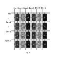
Please refer to FIGS. 3-6. FIG. 3 is a structural diagram of the liquid crystal display panel of present disclosure.
The liquid crystal display panel of this embodiment includes a plurality of data lines Dn−Dn+5, a plurality of scan lines Gn−Gn+3, and a plurality of pixel sets 10. Each of the pixel sets 10 includes two adjacent pixel units. The pixel units which are restricted by a plurality of scan lines are composed in plural rows. The pixel units which are restricted by a plurality of data lines are composed in a plurality of columns. Each one row of the pixel units is disposed with a scan line. Each one column of the pixel units is disposed with a data line.
Referring to FIG. 4, each of the pixel sets 10 includes a first pixel unit 11 and a second pixel unit 12. The first pixel unit 11 includes a first thin film transistor T1, a first storage capacitor CST1, a first liquid crystal capacitor CLC1, a first charging capacitor CS1, and a second charging capacitor CS2. A gate of the first thin film transistor T1 is connected to a corresponding scan line. A source of the first thin film transistor T1 is connected to a corresponding data line. One side of both the first storage capacitor CST1 and the first liquid crystal capacitor CLC1 are connected to the drain of the first thin film transistor T1. The other side of the first storage capacitor CST1 is connected to a common electrode on one side of the array substrate. The other side of the first liquid crystal capacitor CLC1 is connected to a common electrode one side of the color film substrate. One side of the first charging capacitor CS1 is connected to a drain of the first thin film transistor T1. The other side of the first charging capacitor CS1 is connected to one side of the second charging capacitor CS2. The other side of the second charging capacitor is connected to the common electrode on the side of the array substrate.
The second pixel unit includes a second thin film transistor T2, a second storage capacitor CST2, and a second liquid crystal capacitor CLC2. The gate of the second thin film transistor T2 is connected to a corresponding scan line. The source of the second thin film transistor T2 is connected to a corresponding data line. One side of both the second storage capacitor CST2 and the second liquid crystal capacitor CLC2 are connected to the drain of the second thin film transistor T2. The other side of the second storage of the CST2 is connected to a common electrode on the side of the array substrate. The other side of the second liquid crystal capacitor CLC2 is connected to a common electrode on the side of the color film substrate. The drain of the second thin film transistor T2 is still connected to the other side of the first charging capacitor CS1. More specifically, the drain of the second thin film transistor T2 is connected to a node between the first charging capacitor CS1 and the second charging capacitor CS2.
The first pixel unit 11 and the second pixel unit 12 are arranged in alternating rows. For example, a first pixel unit is disposed on the first row, a second pixel unit is disposed on the second row, a first pixel unit is disposed on the third row, a second pixel unit is disposed on the forth row. The first pixel unit 11 and the second pixel unit 12 are disposed on adjacent rows. For example, when the first pixel unit is disposed on the nth row, the second pixel unit is disposed on the (n+1)th row. The liquid crystal display panel includes N rows of pixel where 0<n<N, N≥2.
In the specific driving process shown in FIG. 5, during the period of t2-t3, the scan signal being inputted by Gn is high, the first thin film transistor T1 is closed which makes the voltage of first pixel unit V1 be equal to the data voltage, i.e. high. Therefore the scan signal being inputted by the scan line Gn+1 is low, and the voltage pf the second pixel unit 12 is low. During the period of t3-t4, the signal being inputted by scan line Gn+1 is high, and the second thin film transistor T2 is closed. Keep charging the first charging capacitor CS1 while charging the second pixel unit 12 in order to increase V1, i.e. V1 will be higher than V2. Therefore, the brightness of the first pixel unit 11 is higher than the brightness of the second pixel unit 12, and the viewing angle is increased as well. After the time of t4, V1 and V2 become low since the signal of the scan line is low.
FIG. 6 shows that the display brightness corresponds to FIG. 4. As shown in FIG. 6, H represents that the brightness or voltage of a pixel unit is higher, and L represents that the brightness or voltage of a pixel unit is lower. Since the first pixel unit and the second pixel unit are arranged alternately row by row, all the pixel units at high potential will be located on the same row, and all the pixel units in low potential will be located on the same tow. Therefore, the brightness of the liquid crystal display panel from up to bottom is in the order of high, low, high, low. The manufacturing process will be simplified due to the regular structure of this kind of panel. The liquid crystal display panel divides the voltage of the adjacent pixel units, thus the viewing angle is increased. The colors of each row of pixel units are red, green, blue, red, green, and blue, respectively.
In contrast with the liquid crystal display panel in FIG. 1, the number of TFTs is reduced since each of the pixel units requires only one, instead of three, thin film transistors. The number of capacitors is reduced since each two of the pixel units requires one set of CS1 and CS2, rather than each one of the pixel units requires one set of CS1 and CS2. Therefore the aperture ratio and the transmittance ratio are increased because usage of thin film transistors and capacitors is decreased.
It can be understood that the positions of the first pixel unit 11 and the second pixel unit 12 can be switched.
Please refer to FIG. 7-8. FIG. 7 illustrates the second structural diagram of the liquid crystal display panel of present disclosure.
One main distinction between this embodiment and the above embodiment of the present disclosure is that the first pixel unit 11 and the second pixel unit 12 are arranged alternately. Where in the one of the embodiments, the first pixel unit 11 is disposed on an nth row and a (2k+1)th column (i.e., odd columns), or an (n+1)th row and a (2k)th column (i.e., even columns); the second pixel unit is disposed on an (n+1)th row and a (2k+1)th column, or an nth row and a (2k)th column. The liquid crystal display panel comprises N rows of pixel units where 0<n<N, N≥2, k≥0.
As shown in FIG. 8, the pixel units at high potential and the pixel units in low potential are disposed alternately since the first pixel unit and the second pixel unit are disposed alternately, i.e., the brightness of two adjacent pixel units are different. The light lines and dark lines can be avoided, and thus the display performance is improved on the basis of the first embodiment.
Please refer to FIG. 9-10. FIG. 9 illustrates the third structural diagram of the liquid crystal display panel of present disclosure.
One main distinction between this embodiment and the first embodiment in the present disclosure is that the liquid crystal display panel includes a first region 21 and a second region 22. To improve the prevention of the appearance of the light lines and dark lines, in one of the embodiments, the area of the first region 21 is equal to the area of the second region 22. In one of the embodiment, the first region and the second region are the left part and the right part of the liquid crystal display panel respectively. In another embodiment, the first region and the second region are the upper part and the lower part of the liquid crystal display panel respectively.
The first pixel unit 11 in the first region 21 and the second pixel unit 12 in the second region 22 are located in the same row. The second pixel unit 12 in the first region 21 and the first pixel unit 11 in the second region 22 are located in the same row.
The first pixel unit 11 in the first region 21 and the second pixel unit 12 in the first region 21 are arranged alternately row by row. The first pixel unit 11 in the second region 22 and the second pixel unit in the second region 22 are arranged alternately column by column.
More specifically, when the first pixel unit in the first region 21 is located in the nth row, the second pixel unit in the first region 21 will be located in the (n+1)th row.
When the first pixel unit 11 in the second region 22 is located in the (n+1)th row, the second pixel unit 12 in the second region 22 is located in the nth row.
As shown in FIG. 10, since the positions of the first pixel unit and the second pixel unit are different in the first region and second region, three pixel units at high potential and three pixel units in low potential are located in the same row, i.e., the pixel units at high potential and the pixel units in the low potential are arranged symmetrically; i.e., half of the pixel units of one row have a different brightness from the other half of the pixel units of the same row. On the basis of the first embodiments, the light lines and dark lines are prevented, the pixel units are arranged in order, and the manufacturing procedure is simplified.
It could be understand that the number of the first region and the number of the second region may not be limited to only one. In other embodiments, the liquid crystal display panel includes two of the first regions and one of the second regions. In this situation, the second region is disposed between the two of the first regions. Two of the first regions are disposed on each side of the display panel respectively. In one of the embodiments, the area of two first regions is equal to the area of the second region. In one of the embodiments, the area of two first regions could be not equal to the area of the second region.
The first pixel unit in the two first regions and the second pixel unit in the second region are disposed in the same row; the second pixel unit of the two first regions and the first pixel unit in the second region are disposed in the same row. The first pixel unit in the first region and the second pixel unit in the first region are arranged alternately row by row. The first pixel unit in the second region 22 and the second pixel unit in the second region are arranged alternately column by column.
The present disclosure further provides a liquid crystal display panel which includes a backlight module and any one of the abovementioned liquid crystal display panels.
The liquid crystal display panel and apparatus of present disclosure keeps charging the previous pixel while charging the next pixel, in order to make the brightness of the adjacent pixel units different and increase the viewing angle of the liquid crystal display panel. In addition, the number of the thin film transistors and capacitors is decreased, thus the aperture ratio and transmittance ratio are increased.
In conclusion, although this disclosure has been disclosed through the preferable embodiments above, the preferable embodiments above are not utilized to limit this disclosure. One having ordinary skills can change and modify without violating the concepts and scope of this disclosure. Therefore, the scope that this disclosure protects is based on the scope defined by the claims.

Claims (18)

What is claimed is:
1. A liquid crystal display panel, comprising: a plurality of data lines, a plurality of scan lines, and a plurality of pixel sets comprising a first pixel unit and a second pixel unit; wherein rows of pixel units are arranged with corresponding scan lines, columns of pixels units are arranged with corresponding data lines;
wherein the first pixel unit comprises a first thin film transistor, a first charging capacitor, a second charging capacitor, a first storage capacitor, and a first liquid crystal capacitor; a gate of the first thin film transistor is connected to a corresponding scan line, and a source of the first thin film transistor is connected to a corresponding data line; the first charging capacitor is connected between a drain of the first thin film transistor, and the second charging capacitor; the first storage capacitor and the first liquid crystal capacitor are connected to the drain of the first thin film transistor;
the second pixel unit comprises a second thin film transistor, a second storage capacitor and a second liquid crystal capacitor; a gate of the second thin film transistor is connected to a corresponding scan line, a source of the second thin film transistor is connected to a corresponding data line; a drain of the second thin film transistor is connected to the first charging capacitor, the second storage capacitor and the second liquid crystal capacitor are connected to the drain of the second thin film transistor; wherein a brightness of the first pixel unit is higher than a brightness of the second pixel unit
wherein the liquid crystal display panel comprises a first region and a second region, the first pixel unit of the first region is disposed on a same row as the second pixel unit of the second region; the second pixel unit of the first region is disposed on a same row as the first pixel unit of the second region;
the first pixel unit of the first region is arranged in alternate rows with the second pixel unit of the first region; the first pixel unit of the second region is arranged in alternate rows with the second pixel unit of the second region.
2. The liquid crystal display panel according to claim 1, wherein the first pixel unit and the second pixel unit are arranged in alternate rows.
3. The liquid crystal display panel according to claim 1, wherein the first pixel unit and the second pixel unit are arranged alternately.
4. The liquid crystal display panel according to claim 3, wherein the first pixel unit is disposed on an nth row and a (2k−1)th column and disposed on an (n+1)th row and a (2k)th column; the second pixel unit is disposed on an (n+1)th row and a (2k−1)th column and disposed on an nth row and a (2k)th column, where the liquid crystal display panel comprises N rows of pixel units, where n, k, N are integers, where 0<n<N, N≥2, k≥1.
5. The liquid crystal display panel according to claim 1, wherein an area of the first region is equal to an area of the second region.
6. The liquid crystal display panel according to claim 1, wherein the liquid crystal display panel comprises two first regions and a second region between the two first regions.
7. The liquid crystal display panel according to claim 5, wherein a total area of the two first regions is equal to the area of the second region.
8. A liquid crystal display panel, comprising: a plurality of data lines, a plurality of scan lines, and a plurality of pixel sets comprising a first pixel unit and a second pixel unit; wherein rows of pixel units are arranged with corresponding scan lines, columns of pixels units are arranged with corresponding data lines;
wherein the first pixel unit comprises a first thin film transistor, a first charging capacitor, and a second charging capacitor; a gate of the first thin film transistor is connected to a corresponding scan line, and a source of the first thin film transistor is connected to a corresponding data line; the first charging capacitor is connected between a drain of the first thin film transistor, and the second charging capacitor;
wherein the second pixel unit comprises a second thin film transistor; a gate of the second thin film transistor is connected to a corresponding scan line, a source of the second thin film transistor is connected to a corresponding data line; a drain of the second thin film transistor is connected to the first charging capacitor;
wherein the liquid crystal display panel comprises a first region and a second region, the first pixel unit of the first region is disposed on a same row with the second pixel unit of the second region; the second pixel unit of the first region is disposed on a same row with the first pixel unit of the second region;
the first pixel unit of the first region is arranged in alternate rows with the second pixel unit of the first region; the first pixel unit of the second region is arranged in alternate rows with the second pixel unit of the second region.
9. The liquid crystal display panel according to claim 8, wherein the first pixel unit and the second pixel unit are arranged in alternate rows.
10. The liquid crystal display panel according to claim 8, wherein the first pixel unit and the second pixel unit are arranged alternately.
11. The liquid crystal display panel according to claim 10, wherein the first pixel unit is disposed on an nth row and a (2k−1)th column and disposed on an (n+1) row and a (2k)th column; the second pixel unit is disposed on an (n+1)th row and a (2k−1)th column and disposed on an nth row and a (2k)th column, where the liquid crystal display panel comprises N rows of pixel units, where n, k, N are integers, where 0<n<N, N≥2, k≥1.
12. The liquid crystal display panel according to claim 8, wherein an area of the first region is equal to an area of the second region.
13. The liquid crystal display panel according to claim 8, wherein the liquid crystal display panel comprises two first regions and a second region between the two first regions.
14. The liquid crystal display panel according to claim 13, wherein a total area of the two first regions is equal to the area of the second region.
15. The liquid crystal display panel according to claim 8, wherein the brightness of the first pixel unit is higher than a brightness of the second pixel unit.
16. A liquid crystal display device comprising a backlight module; and
a liquid crystal display panel comprising: a plurality of data lines, a plurality of scan lines, and a plurality of pixel sets comprising a first pixel unit and a second pixel unit; wherein rows of pixel units are arranged with corresponding scan lines, columns of pixels units are arranged with corresponding data lines;
wherein the first pixel unit comprises a first thin film transistor, a first charging capacitor, and a second charging capacitor; a gate of the first thin film transistor is connected to a corresponding scan line, a source of the first thin film transistor is connected to a corresponding data line; the first charging capacitor is connected between a drain of the first thin film transistor, and the second charging capacitor;
the second pixel unit comprises a second thin film transistor; a gate of the second thin film transistor is connected to a corresponding scan line, a source of the second thin film transistor is connected to a corresponding data line; a drain of the second thin film transistor is connected to the first charging capacitor;
wherein the liquid crystal display panel comprises a first region and a second region, the first pixel unit of the first region is disposed on a same row as the second pixel unit of the second region; the second pixel unit of the first region is disposed on a same row as the first pixel unit of the second region;
the first pixel unit of the first region is arranged in alternate rows with the second pixel unit of the first region; the first pixel unit of the second region is arranged in alternate rows with the second pixel unit of the second region.
17. The liquid crystal display device according to claim 16, wherein the first pixel unit and the second pixel unit are arranged in alternate rows.
18. The liquid crystal display device according to claim 16, wherein the first pixel unit and the second pixel unit are arranged alternately.
US15/572,821 2017-06-07 2017-11-02 Liquid crystal display panel and apparatus Active US10310306B2 (en)

Applications Claiming Priority (4)

Application Number Priority Date Filing Date Title
CN201710423649 2017-06-07
CN201710423649.8A CN107045240B (en) 2017-06-07 2017-06-07 A kind of liquid crystal display panel and device
CN201710423649.8 2017-06-07
PCT/CN2017/109085 WO2018223591A1 (en) 2017-06-07 2017-11-02 Liquid crystal display panel and device

Publications (2)

Publication Number Publication Date
US20180356662A1 US20180356662A1 (en) 2018-12-13
US10310306B2 true US10310306B2 (en) 2019-06-04

Family

ID=64564115

Family Applications (1)

Application Number Title Priority Date Filing Date
US15/572,821 Active US10310306B2 (en) 2017-06-07 2017-11-02 Liquid crystal display panel and apparatus

Country Status (1)

Country Link
US (1) US10310306B2 (en)

Families Citing this family (2)

* Cited by examiner, † Cited by third party
Publication number Priority date Publication date Assignee Title
US10714043B2 (en) * 2018-09-19 2020-07-14 Chongqing Hkc Optoelectronics Technology Co., Ltd. Display device and liquid crystal display
CN109307942A (en) * 2018-10-30 2019-02-05 惠科股份有限公司 A kind of display panel, display device and production method

Citations (3)

* Cited by examiner, † Cited by third party
Publication number Priority date Publication date Assignee Title
US20080106660A1 (en) * 2004-12-28 2008-05-08 Masae Kitayama Liquid Crystal Display Device and Method for Driving the Same
US20090195487A1 (en) * 2006-08-24 2009-08-06 Fumikazu Shimoshikiryoh Liquid crystal display device
US20170045789A1 (en) * 2014-06-04 2017-02-16 Sakai Display Products Corporation Display Apparatus

Patent Citations (3)

* Cited by examiner, † Cited by third party
Publication number Priority date Publication date Assignee Title
US20080106660A1 (en) * 2004-12-28 2008-05-08 Masae Kitayama Liquid Crystal Display Device and Method for Driving the Same
US20090195487A1 (en) * 2006-08-24 2009-08-06 Fumikazu Shimoshikiryoh Liquid crystal display device
US20170045789A1 (en) * 2014-06-04 2017-02-16 Sakai Display Products Corporation Display Apparatus

Also Published As

Publication number Publication date
US20180356662A1 (en) 2018-12-13

Similar Documents

Publication Publication Date Title
US20210142747A1 (en) Array substrate, display panel, display device, and driving methods thereof
US8248343B2 (en) Liquid crystal display panel and method for driving pixels thereof
US11475857B2 (en) Array substrate and display device
US10297213B2 (en) Array substrate with data line sharing structure
CN108646480B (en) Vertical alignment type liquid crystal display
US9857650B2 (en) Array substrate and liquid crystal display panel including the same
US9772534B2 (en) Liquid crystal display
CN111025770B (en) Manufacturing method of display panel and electronic equipment
CN109283756A (en) Multidomain liquid crystal display
US10073312B2 (en) Structure for LCD panel
US10657911B2 (en) Vertical alignment liquid crystal display
EP3637182A1 (en) Liquid crystal display panel and device
US10203575B2 (en) Array substrate and liquid crystal panel
US10789894B2 (en) Drive method for display panel
US10310306B2 (en) Liquid crystal display panel and apparatus
US10591792B2 (en) Liquid crystal display panel and device
US20180143472A1 (en) Array substrate and display panel
US9715859B2 (en) LCD panel of dot inversion mode
CN109300441A (en) Multidomain dot structure
CN111381408B (en) Pixel array and liquid crystal panel thereof
CN108761936B (en) Vertical alignment type liquid crystal display
US10755653B2 (en) Vertical alignment liquid crystal display
US20240029681A1 (en) Display panel and display device
US20190304383A1 (en) Liquid crystal display
US20200302846A1 (en) Driving method for display panel

Legal Events

Date Code Title Description
AS Assignment

Owner name: SHENZHEN CHINA STAR OPTOELECTRONICS SEMICONDUCTOR

Free format text: ASSIGNMENT OF ASSIGNORS INTEREST;ASSIGNOR:HAO, SIKUN;REEL/FRAME:044078/0459

Effective date: 20171011

FEPP Fee payment procedure

Free format text: ENTITY STATUS SET TO UNDISCOUNTED (ORIGINAL EVENT CODE: BIG.); ENTITY STATUS OF PATENT OWNER: LARGE ENTITY

STPP Information on status: patent application and granting procedure in general

Free format text: NOTICE OF ALLOWANCE MAILED -- APPLICATION RECEIVED IN OFFICE OF PUBLICATIONS

STPP Information on status: patent application and granting procedure in general

Free format text: PUBLICATIONS -- ISSUE FEE PAYMENT VERIFIED

STCF Information on status: patent grant

Free format text: PATENTED CASE

MAFP Maintenance fee payment

Free format text: PAYMENT OF MAINTENANCE FEE, 4TH YEAR, LARGE ENTITY (ORIGINAL EVENT CODE: M1551); ENTITY STATUS OF PATENT OWNER: LARGE ENTITY

Year of fee payment: 4