US10692417B2 - Display apparatus - Google Patents

Display apparatus Download PDF

Info

Publication number
US10692417B2
US10692417B2 US16/015,359 US201816015359A US10692417B2 US 10692417 B2 US10692417 B2 US 10692417B2 US 201816015359 A US201816015359 A US 201816015359A US 10692417 B2 US10692417 B2 US 10692417B2
Authority
US
United States
Prior art keywords
group
color
display apparatus
light
dopant
Prior art date
Legal status (The legal status is an assumption and is not a legal conclusion. Google has not performed a legal analysis and makes no representation as to the accuracy of the status listed.)
Active, expires
Application number
US16/015,359
Other versions
US20180374409A1 (en
Inventor
Sangyoon Lee
Sunghun Lee
Shinae Jun
Chilhee CHUNG
Byoungki CHOI
Intaek Han
Current Assignee (The listed assignees may be inaccurate. Google has not performed a legal analysis and makes no representation or warranty as to the accuracy of the list.)
Samsung Electronics Co Ltd
Original Assignee
Samsung Electronics Co Ltd
Priority date (The priority date is an assumption and is not a legal conclusion. Google has not performed a legal analysis and makes no representation as to the accuracy of the date listed.)
Filing date
Publication date
Priority claimed from KR1020170116255A external-priority patent/KR102477097B1/en
Application filed by Samsung Electronics Co Ltd filed Critical Samsung Electronics Co Ltd
Publication of US20180374409A1 publication Critical patent/US20180374409A1/en
Assigned to SAMSUNG ELECTRONICS CO., LTD. reassignment SAMSUNG ELECTRONICS CO., LTD. ASSIGNMENT OF ASSIGNORS INTEREST (SEE DOCUMENT FOR DETAILS). Assignors: CHOI, BYOUNGKI, CHUNG, CHILHEE, HAN, Intaek, JUN, SHINAE, LEE, SANGYOON, LEE, SUNGHUN
Priority to US16/857,693 priority Critical patent/US11562678B2/en
Application granted granted Critical
Publication of US10692417B2 publication Critical patent/US10692417B2/en
Priority to US17/936,900 priority patent/US11688322B2/en
Active legal-status Critical Current
Adjusted expiration legal-status Critical

Links

Images

Classifications

    • HELECTRICITY
    • H10SEMICONDUCTOR DEVICES; ELECTRIC SOLID-STATE DEVICES NOT OTHERWISE PROVIDED FOR
    • H10KORGANIC ELECTRIC SOLID-STATE DEVICES
    • H10K59/00Integrated devices, or assemblies of multiple devices, comprising at least one organic light-emitting element covered by group H10K50/00
    • H10K59/30Devices specially adapted for multicolour light emission
    • H10K59/38Devices specially adapted for multicolour light emission comprising colour filters or colour changing media [CCM]
    • GPHYSICS
    • G09EDUCATION; CRYPTOGRAPHY; DISPLAY; ADVERTISING; SEALS
    • G09GARRANGEMENTS OR CIRCUITS FOR CONTROL OF INDICATING DEVICES USING STATIC MEANS TO PRESENT VARIABLE INFORMATION
    • G09G3/00Control arrangements or circuits, of interest only in connection with visual indicators other than cathode-ray tubes
    • G09G3/20Control arrangements or circuits, of interest only in connection with visual indicators other than cathode-ray tubes for presentation of an assembly of a number of characters, e.g. a page, by composing the assembly by combination of individual elements arranged in a matrix no fixed position being assigned to or needed to be assigned to the individual characters or partial characters
    • G09G3/22Control arrangements or circuits, of interest only in connection with visual indicators other than cathode-ray tubes for presentation of an assembly of a number of characters, e.g. a page, by composing the assembly by combination of individual elements arranged in a matrix no fixed position being assigned to or needed to be assigned to the individual characters or partial characters using controlled light sources
    • G09G3/30Control arrangements or circuits, of interest only in connection with visual indicators other than cathode-ray tubes for presentation of an assembly of a number of characters, e.g. a page, by composing the assembly by combination of individual elements arranged in a matrix no fixed position being assigned to or needed to be assigned to the individual characters or partial characters using controlled light sources using electroluminescent panels
    • G09G3/32Control arrangements or circuits, of interest only in connection with visual indicators other than cathode-ray tubes for presentation of an assembly of a number of characters, e.g. a page, by composing the assembly by combination of individual elements arranged in a matrix no fixed position being assigned to or needed to be assigned to the individual characters or partial characters using controlled light sources using electroluminescent panels semiconductive, e.g. using light-emitting diodes [LED]
    • G09G3/3208Control arrangements or circuits, of interest only in connection with visual indicators other than cathode-ray tubes for presentation of an assembly of a number of characters, e.g. a page, by composing the assembly by combination of individual elements arranged in a matrix no fixed position being assigned to or needed to be assigned to the individual characters or partial characters using controlled light sources using electroluminescent panels semiconductive, e.g. using light-emitting diodes [LED] organic, e.g. using organic light-emitting diodes [OLED]
    • G09G3/3225Control arrangements or circuits, of interest only in connection with visual indicators other than cathode-ray tubes for presentation of an assembly of a number of characters, e.g. a page, by composing the assembly by combination of individual elements arranged in a matrix no fixed position being assigned to or needed to be assigned to the individual characters or partial characters using controlled light sources using electroluminescent panels semiconductive, e.g. using light-emitting diodes [LED] organic, e.g. using organic light-emitting diodes [OLED] using an active matrix
    • GPHYSICS
    • G09EDUCATION; CRYPTOGRAPHY; DISPLAY; ADVERTISING; SEALS
    • G09GARRANGEMENTS OR CIRCUITS FOR CONTROL OF INDICATING DEVICES USING STATIC MEANS TO PRESENT VARIABLE INFORMATION
    • G09G3/00Control arrangements or circuits, of interest only in connection with visual indicators other than cathode-ray tubes
    • G09G3/20Control arrangements or circuits, of interest only in connection with visual indicators other than cathode-ray tubes for presentation of an assembly of a number of characters, e.g. a page, by composing the assembly by combination of individual elements arranged in a matrix no fixed position being assigned to or needed to be assigned to the individual characters or partial characters
    • G09G3/2003Display of colours
    • H01L27/3209
    • H01L27/322
    • H01L27/3244
    • H01L51/5016
    • H01L51/504
    • HELECTRICITY
    • H10SEMICONDUCTOR DEVICES; ELECTRIC SOLID-STATE DEVICES NOT OTHERWISE PROVIDED FOR
    • H10KORGANIC ELECTRIC SOLID-STATE DEVICES
    • H10K50/00Organic light-emitting devices
    • H10K50/10OLEDs or polymer light-emitting diodes [PLED]
    • H10K50/11OLEDs or polymer light-emitting diodes [PLED] characterised by the electroluminescent [EL] layers
    • H10K50/12OLEDs or polymer light-emitting diodes [PLED] characterised by the electroluminescent [EL] layers comprising dopants
    • HELECTRICITY
    • H10SEMICONDUCTOR DEVICES; ELECTRIC SOLID-STATE DEVICES NOT OTHERWISE PROVIDED FOR
    • H10KORGANIC ELECTRIC SOLID-STATE DEVICES
    • H10K50/00Organic light-emitting devices
    • H10K50/10OLEDs or polymer light-emitting diodes [PLED]
    • H10K50/11OLEDs or polymer light-emitting diodes [PLED] characterised by the electroluminescent [EL] layers
    • H10K50/125OLEDs or polymer light-emitting diodes [PLED] characterised by the electroluminescent [EL] layers specially adapted for multicolour light emission, e.g. for emitting white light
    • H10K50/13OLEDs or polymer light-emitting diodes [PLED] characterised by the electroluminescent [EL] layers specially adapted for multicolour light emission, e.g. for emitting white light comprising stacked EL layers within one EL unit
    • HELECTRICITY
    • H10SEMICONDUCTOR DEVICES; ELECTRIC SOLID-STATE DEVICES NOT OTHERWISE PROVIDED FOR
    • H10KORGANIC ELECTRIC SOLID-STATE DEVICES
    • H10K59/00Integrated devices, or assemblies of multiple devices, comprising at least one organic light-emitting element covered by group H10K50/00
    • H10K59/10OLED displays
    • H10K59/12Active-matrix OLED [AMOLED] displays
    • H10K59/131Interconnections, e.g. wiring lines or terminals
    • HELECTRICITY
    • H10SEMICONDUCTOR DEVICES; ELECTRIC SOLID-STATE DEVICES NOT OTHERWISE PROVIDED FOR
    • H10KORGANIC ELECTRIC SOLID-STATE DEVICES
    • H10K59/00Integrated devices, or assemblies of multiple devices, comprising at least one organic light-emitting element covered by group H10K50/00
    • H10K59/30Devices specially adapted for multicolour light emission
    • H10K59/32Stacked devices having two or more layers, each emitting at different wavelengths
    • GPHYSICS
    • G09EDUCATION; CRYPTOGRAPHY; DISPLAY; ADVERTISING; SEALS
    • G09GARRANGEMENTS OR CIRCUITS FOR CONTROL OF INDICATING DEVICES USING STATIC MEANS TO PRESENT VARIABLE INFORMATION
    • G09G2300/00Aspects of the constitution of display devices
    • G09G2300/04Structural and physical details of display devices
    • G09G2300/0439Pixel structures
    • G09G2300/0452Details of colour pixel setup, e.g. pixel composed of a red, a blue and two green components
    • GPHYSICS
    • G09EDUCATION; CRYPTOGRAPHY; DISPLAY; ADVERTISING; SEALS
    • G09GARRANGEMENTS OR CIRCUITS FOR CONTROL OF INDICATING DEVICES USING STATIC MEANS TO PRESENT VARIABLE INFORMATION
    • G09G2320/00Control of display operating conditions
    • G09G2320/06Adjustment of display parameters
    • G09G2320/0666Adjustment of display parameters for control of colour parameters, e.g. colour temperature
    • H01L2251/5369
    • H01L2251/552
    • H01L51/0085
    • H01L51/0087
    • H01L51/5268
    • H01L51/5271
    • H01L51/5278
    • HELECTRICITY
    • H10SEMICONDUCTOR DEVICES; ELECTRIC SOLID-STATE DEVICES NOT OTHERWISE PROVIDED FOR
    • H10KORGANIC ELECTRIC SOLID-STATE DEVICES
    • H10K2101/00Properties of the organic materials covered by group H10K85/00
    • H10K2101/10Triplet emission
    • HELECTRICITY
    • H10SEMICONDUCTOR DEVICES; ELECTRIC SOLID-STATE DEVICES NOT OTHERWISE PROVIDED FOR
    • H10KORGANIC ELECTRIC SOLID-STATE DEVICES
    • H10K2101/00Properties of the organic materials covered by group H10K85/00
    • H10K2101/20Delayed fluorescence emission
    • HELECTRICITY
    • H10SEMICONDUCTOR DEVICES; ELECTRIC SOLID-STATE DEVICES NOT OTHERWISE PROVIDED FOR
    • H10KORGANIC ELECTRIC SOLID-STATE DEVICES
    • H10K2101/00Properties of the organic materials covered by group H10K85/00
    • H10K2101/30Highest occupied molecular orbital [HOMO], lowest unoccupied molecular orbital [LUMO] or Fermi energy values
    • HELECTRICITY
    • H10SEMICONDUCTOR DEVICES; ELECTRIC SOLID-STATE DEVICES NOT OTHERWISE PROVIDED FOR
    • H10KORGANIC ELECTRIC SOLID-STATE DEVICES
    • H10K2102/00Constructional details relating to the organic devices covered by this subclass
    • H10K2102/301Details of OLEDs
    • H10K2102/331Nanoparticles used in non-emissive layers, e.g. in packaging layer
    • HELECTRICITY
    • H10SEMICONDUCTOR DEVICES; ELECTRIC SOLID-STATE DEVICES NOT OTHERWISE PROVIDED FOR
    • H10KORGANIC ELECTRIC SOLID-STATE DEVICES
    • H10K50/00Organic light-emitting devices
    • H10K50/10OLEDs or polymer light-emitting diodes [PLED]
    • H10K50/19Tandem OLEDs
    • HELECTRICITY
    • H10SEMICONDUCTOR DEVICES; ELECTRIC SOLID-STATE DEVICES NOT OTHERWISE PROVIDED FOR
    • H10KORGANIC ELECTRIC SOLID-STATE DEVICES
    • H10K50/00Organic light-emitting devices
    • H10K50/80Constructional details
    • H10K50/85Arrangements for extracting light from the devices
    • H10K50/854Arrangements for extracting light from the devices comprising scattering means
    • HELECTRICITY
    • H10SEMICONDUCTOR DEVICES; ELECTRIC SOLID-STATE DEVICES NOT OTHERWISE PROVIDED FOR
    • H10KORGANIC ELECTRIC SOLID-STATE DEVICES
    • H10K50/00Organic light-emitting devices
    • H10K50/80Constructional details
    • H10K50/85Arrangements for extracting light from the devices
    • H10K50/856Arrangements for extracting light from the devices comprising reflective means
    • HELECTRICITY
    • H10SEMICONDUCTOR DEVICES; ELECTRIC SOLID-STATE DEVICES NOT OTHERWISE PROVIDED FOR
    • H10KORGANIC ELECTRIC SOLID-STATE DEVICES
    • H10K59/00Integrated devices, or assemblies of multiple devices, comprising at least one organic light-emitting element covered by group H10K50/00
    • H10K59/80Constructional details
    • H10K59/875Arrangements for extracting light from the devices
    • H10K59/877Arrangements for extracting light from the devices comprising scattering means
    • HELECTRICITY
    • H10SEMICONDUCTOR DEVICES; ELECTRIC SOLID-STATE DEVICES NOT OTHERWISE PROVIDED FOR
    • H10KORGANIC ELECTRIC SOLID-STATE DEVICES
    • H10K59/00Integrated devices, or assemblies of multiple devices, comprising at least one organic light-emitting element covered by group H10K50/00
    • H10K59/80Constructional details
    • H10K59/875Arrangements for extracting light from the devices
    • H10K59/878Arrangements for extracting light from the devices comprising reflective means
    • HELECTRICITY
    • H10SEMICONDUCTOR DEVICES; ELECTRIC SOLID-STATE DEVICES NOT OTHERWISE PROVIDED FOR
    • H10KORGANIC ELECTRIC SOLID-STATE DEVICES
    • H10K85/00Organic materials used in the body or electrodes of devices covered by this subclass
    • H10K85/30Coordination compounds
    • H10K85/341Transition metal complexes, e.g. Ru(II)polypyridine complexes
    • H10K85/342Transition metal complexes, e.g. Ru(II)polypyridine complexes comprising iridium
    • HELECTRICITY
    • H10SEMICONDUCTOR DEVICES; ELECTRIC SOLID-STATE DEVICES NOT OTHERWISE PROVIDED FOR
    • H10KORGANIC ELECTRIC SOLID-STATE DEVICES
    • H10K85/00Organic materials used in the body or electrodes of devices covered by this subclass
    • H10K85/30Coordination compounds
    • H10K85/341Transition metal complexes, e.g. Ru(II)polypyridine complexes
    • H10K85/346Transition metal complexes, e.g. Ru(II)polypyridine complexes comprising platinum

Definitions

  • the present disclosure relates to display apparatuses.
  • OLED Organic light-emitting devices
  • An OLED may include an anode, a cathode, and an emission layer (organic material-containing emission layer) interposed therebetween.
  • a hole transport area may be provided between the anode and the emission layer, and an electron transport area may be provided between the emission layer and the cathode.
  • Holes injected from the anode may be transferred to the emission layer by passing through the hole transport area, and electrons injected from the cathode may be transferred to the emission layer by passing through the electron transport area.
  • excitons may be generated.
  • the excitons are shifted from an excited state to a ground state, light may be generated.
  • a blue OLED substrate or a white OLED substrate is mainly used as a light source.
  • display apparatuses including an OLED light source that emits green light.
  • display apparatuses including an OLED light source that emits a green light and a blue light, a plurality of quantum-dot color-converters, and a plurality of color filter elements.
  • a display apparatus includes:
  • an OLED (organic light-emitting device) substrate comprising a structure in which at least one blue light-emitting unit and at least one green light-emitting unit are stacked, wherein the OLED substrate generates a mixed light of a blue light and a green light;
  • a color controller provided on the OLED substrate to adjust color of a light generated from the OLED substrate
  • the color controller includes:
  • a first color control element including a plurality of first quantum dots for green conversion
  • a second color control element including a plurality of second quantum dots for red conversion
  • a third color control element for presenting a blue color
  • the OLED substrate may include a tandem structure.
  • the OLED substrate may include:
  • the green light-emitting unit may be arranged between the first and second blue light-emitting units.
  • the display apparatus may further include:
  • a second charge generation layer provided between the green light-emitting unit and the second blue light-emitting unit.
  • the green light-emitting unit may include a green emission layer including an organic material, and the green emission layer may include a thermally activated delayed fluorescence (TADF) dopant.
  • TADF thermally activated delayed fluorescence
  • the green light-emitting unit may include a green emission layer including an organic material, the green emission layer may include a phosphorescent dopant, and the phosphorescent dopant may satisfy T1 (dopant) ⁇ S1 (dopant) ⁇ T1 (dopant)+0.5 electron Volts, wherein the T1 (dopant) is a triplet energy level (expressed in electron Volts) of the dopant and the S1 (dopant) is a singlet energy level (expressed in electron Volts) of the dopant.
  • the dopant may be an organic metal compound containing iridium (Ir).
  • the dopant may be an organic metal compound containing at least one of platinum (Pt), osmium (Os), titanium (Ti), zirconium (Zr), hafnium (Hf), europium (Eu), terbium (Tb), thulium (Tm), rhodium (Rh), ruthenium (Ru), rhenium (Re), beryllium (Be), magnesium (Mg), aluminum (Al), calcium (Ca), manganese (Mn), cobalt (Co), copper (Cu), zinc (Zn), gallium (Ga), germanium (Ge), palladium (Pd), silver (Ag), and gold (Au).
  • the dopant may be an organic metal compound having a square-planar coordination structure.
  • the dopant may include a metal M and an organic ligand, and the metal M and the organic ligand form one, two, or three cyclometallated rings.
  • the dopant may include a metal M and a four-coordinate organic ligand that forms three or four cyclometallated rings
  • the metal M may include platinum (Pt), osmium (Os), titanium (Ti), zirconium (Zr), hafnium (Hf), europium (Eu), terbium (Tb), thulium (Tm), rhodium (Rh), ruthenium (Ru), rhenium (Re), beryllium (Be), magnesium (Mg), aluminum (Al), calcium (Ca), manganese (Mn), cobalt (Co), copper (Cu), zinc (Zn), gallium (Ga), germanium (Ge), palladium (Pd), silver (Ag), or gold (Au), and the four-coordinate organic ligand may include a benzimidazole group or a pyridine group.
  • the first color filter may be a blue cut filter
  • the second color filter may be a blue and green cut filter
  • the first color filter may be an absorption type green color filter
  • the second color filter may be an absorption type red color filter
  • the third color control element may include a blue color filter, and the display apparatus may further include a light scattering element provided between the blue color filter and the OLED substrate.
  • the third color control element may include a color converter comprising third quantum dots for blue conversion, and the display apparatus may further include a third color filter provided on the third color control element.
  • the third color filter may be a green cut filter or an absorption type blue color filter.
  • a core part of the second quantum dot may have a size greater than a core part of the first quantum dot.
  • the first color control element may correspond to a first sub-pixel area
  • the second color control element may correspond to a second sub-pixel area
  • the third color control element may correspond to a third sub-pixel area
  • the display apparatus may further include a fourth sub-pixel area, wherein the fourth sub-pixel area produces a color other than colors of the first to third sub-pixel areas.
  • the fourth sub-pixel area may be a blank area on the OLED substrate without a color control element, or may include a light scattering element provided on the OLED substrate.
  • the display apparatus may further include a selective reflection film provided between the OLED substrate and the color controller.
  • the selective reflection film may be configured to transmit a blue light and a green light and to reflect a red light.
  • the display apparatus may further include a thin film transistor (TFT) array substrate having a plurality of thin film transistors to drive pixel areas of the OLED substrate.
  • TFT thin film transistor
  • FIG. 1 is a cross-sectional view of a display apparatus according to an embodiment
  • FIG. 2 is a cross-sectional view of a display apparatus according to another embodiment
  • FIG. 3 is a cross-sectional view of a display apparatus according to another embodiment
  • FIG. 4 is a cross-sectional view of a display apparatus according to another embodiment
  • FIG. 5 is a cross-sectional view of a display apparatus according to another embodiment
  • FIG. 6 is a cross-sectional view of a display apparatus according to another embodiment
  • FIG. 7 is a cross-sectional view of a display apparatus according to another embodiment.
  • FIG. 8 is a cross-sectional view of a display apparatus according to another embodiment.
  • FIG. 9 is a cross-sectional view illustrating in detail a configuration of a display apparatus according to another embodiment.
  • FIG. 10 is a cross-sectional view illustrating in detail a configuration of an OLED substrate that is applicable to a display apparatus according to an embodiment
  • FIG. 11 is a cross-sectional view illustrating in detail a configuration of a display apparatus according to an embodiment
  • FIG. 12 is a graph of photoluminescence (PL) quantum yield (percent, %) versus wavelength (nanometer, nm) showing a photoluminescence (PL) quantum yield according to wavelengths of a Green-QD containing color converter and a Red-QD containing color converter that are applicable to a display apparatus according to an embodiment;
  • FIG. 13 is a graph of transmittance (percent, %) versus wavelength (nanometer, nm) showing a change in the transmittance according to wavelengths of a Green-QD containing color converter and a Red-QD containing color converter that are applicable to a display apparatus according to an embodiment;
  • FIG. 14 is a graph of radiance (watt per steradian per square meter per nanometer, W/sr/m 2 /nm) versus wavelength (nanometer, nm) showing the emission spectrum of an OLED substrate that is applicable to a display apparatus according to an embodiment;
  • FIG. 15 is a graph of radiance (watt per steradian per square meter per nanometer, W/sr/m 2 /nm) versus wavelength (nanometer, nm) showing the emission spectrum of a light that is emitted from an OLED substrate (light source) and then passes through a Green-QD containing color converter, according to an embodiment;
  • FIG. 16 is a graph of radiance (watt per steradian per square meter per nanometer, W/sr/m 2 /nm) versus wavelength (nanometer, nm) showing the emission spectrum of a light that is emitted from the OLED substrate (light source) and then passes through a Red-QD containing color converter, according to an embodiment;
  • FIG. 17 is a graph of transmittance (percent, %) versus wavelength (nanometer, nm) showing a change in transmittance (%) according to the wavelength of an absorption type color filter that is applicable to a display apparatus according to an embodiment
  • FIG. 18 is a graph of transmittance (percent, %) versus wavelength (nanometer, nm) showing a change in transmittance (%) according to the wavelength of a cut-off type color filter that is applicable to a display apparatus according to an embodiment
  • FIG. 19 is a graph of transmittance (percent, %) versus wavelength (nanometer, nm) showing a change in transmittance (%) according to the wavelength of an absorption type color filter that is applicable to a display apparatus according to an embodiment
  • FIG. 20 is a graph of spectral radiance (watt per square meter steradian nanometer, W/m 2 ⁇ sr ⁇ nm) versus wavelength (nanometer, nm) showing a difference in spectral radiance between an embodiment in which a light scattering agent is used with respect to blue light and an embodiment in which the light scattering agent is not used with respect to the blue light;
  • FIG. 21 is a graph showing a change in current efficiency (candelas per ampere, cd/A) according to various conditions regarding a display apparatus.
  • FIG. 22 is a graph showing a change in color characteristics (percent, %) according to various conditions regarding a display apparatus.
  • first”, “second”, etc. may be used herein to describe various elements, components, regions, layers and/or sections, these elements, components, regions, layers and/or sections should not be limited by these terms. These terms are only used to distinguish one element, component, region, layer or section from another element, component, region, layer or section. Thus, a first element, component, region, layer or section discussed below could be termed a second element, component, region, layer or section without departing from the teachings of exemplary embodiments.
  • spatially relative terms such as “beneath,” “below,” “lower,” “above,” “upper” and the like, may be used herein for ease of description to describe one element or feature's relationship to another element(s) or feature(s) as illustrated in the figures. It will be understood that the spatially relative terms are intended to encompass different orientations of the device in use or operation in addition to the orientation depicted in the figures. For example, if the device in the figures is turned over, elements described as “below” or “beneath” other elements or features would then be oriented “above” the other elements or features. Thus, the exemplary term “below” can encompass both an orientation of above and below. The device may be otherwise oriented (rotated 90 degrees or at other orientations) and the spatially relative descriptors used herein interpreted accordingly.
  • Exemplary embodiments are described herein with reference to cross-sectional illustrations that are schematic illustrations of idealized embodiments (and intermediate structures) of exemplary embodiments. As such, variations from the shapes of the illustrations as a result, for example, of manufacturing techniques and/or tolerances, are to be expected. Thus, exemplary embodiments should not be construed as limited to the particular shapes of regions illustrated herein but are to include deviations in shapes that result, for example, from manufacturing. For example, an implanted region illustrated as a rectangle will, typically, have rounded or curved features and/or a gradient of implant concentration at its edges rather than a binary change from implanted to non-implanted region.
  • a buried region formed by implantation may result in some implantation in the region between the buried region and the surface through which the implantation takes place.
  • the regions illustrated in the figures are schematic in nature and their shapes are not intended to illustrate the actual shape of a region of a device and are not intended to limit the scope of exemplary embodiments.
  • FIG. 1 is a cross-sectional view of a display apparatus according to an embodiment.
  • the display apparatus may include an organic light-emitting device (OLED) substrate 100 and a color controller 200 for controlling color of a light generated from the OLED substrate 100 .
  • OLED organic light-emitting device
  • the OLED substrate 100 may be referred to as an OLED light source.
  • the OLED substrate 100 may have a structure in which at least one blue light-emitting unit and at least one green light-emitting unit are stacked.
  • the blue light-emitting unit may emit a blue light having a peak wavelength range of about 440 nanometers (nm) to about 500 nm or about 450 nm to about 480 nm
  • the green light-emitting unit may emit a green light having a peak wavelength range of about 500 nm to about 550 nm or about 510 nm to about 540 nm.
  • the OLED substrate 100 may emit a mixed light of a blue light and a green light.
  • the blue light-emitting unit may include a blue fluorescent material and/or a blue phosphorescent material.
  • the green light-emitting unit may include a green phosphorescent material and/or a green fluorescent material.
  • the OLED substrate 100 may include a first blue light-emitting unit 20 , a green light-emitting unit 30 , and a second blue light-emitting unit 40 .
  • the green light-emitting unit 30 may be arranged between the first blue light-emitting unit 20 and the second blue light-emitting unit 40 .
  • the green light-emitting unit 30 and the second blue light-emitting unit 40 may be sequentially stacked over the first blue light-emitting unit 20 .
  • each of the first and second blue light-emitting units 20 and 40 may be shorter than that of the green light-emitting unit 30 , it may be advantageous to use two or more blue light-emitting units, that is, the first and second blue light-emitting units 20 and 40 , and a less number of green light-emitting units, that is, the green light-emitting unit 30 .
  • the single green light-emitting unit 30 may be used between the two first and second blue light-emitting units 20 and 40 .
  • the configuration of the OLED substrate 100 may be changed in various ways.
  • the OLED substrate 100 may have a tandem structure. In this state, a first charge generation layer (not shown) may be provided between the first blue light-emitting unit 20 and the green light-emitting unit 30 . Furthermore, a second charge generation layer (not shown) may be provided between the green light-emitting unit 30 and the second blue light-emitting unit 40 .
  • the above-described tandem structure and the first and second charge generation layers are described below in detail with reference to FIGS. 9 and 10 .
  • the OLED substrate 100 may further include a lower layer under the first blue light-emitting unit 20 and an upper layer over the second blue light-emitting unit 40 . Although in FIG. 1 no separate reference numerals are assigned to the lower layer and upper layer, these elements may be regarded as the elements included in the OLED substrate 100 .
  • the lower layer and upper layer are described below in detail with reference to FIGS. 9 and 11 .
  • the color controller 200 may be provided on one surface of the OLED substrate 100 .
  • the color controller 200 may include a first color control element 70 a including a plurality of first quantum dots (QDs) for green conversion, a second color control element 70 b including a plurality of second QDs for red conversion, and a third color control element 75 c including a plurality of third quantum dots for presenting a blue color.
  • the color controller 200 may further include a first color filter 80 a provided on the first color control element 70 a and a second color filter 80 b provided on the second color control element 70 b.
  • the first color control element 70 a may be a Green-QD containing layer and may convert the light generated from the OLED substrate 100 into a green G light.
  • the second color control element 70 b may be a Red-QD containing layer and may convert the light generated from the OLED substrate 100 into a red R light.
  • the first color control element 70 a may be referred to as the first color converter (or color conversion element)
  • the second color control element 70 b may be referred to as the second color converter (or color conversion element).
  • the color converter may be formed by mixing a resin material, QDs, and a light scattering agent.
  • the resin material may include, for example, a photoresist (PR) material.
  • the third color control element 75 c may be a color filter that selectively passes a blue B wavelength range of the light generated from the OLED substrate 100 .
  • the third color control element 75 c may be a Blue-color filter (C/F).
  • the third color control element 75 c may be an absorption type color filter including a pigment or dye, or QDs.
  • the absorption type color filter may absorb a light of a wavelength range other than a light of a target wavelength range.
  • the first color filter 80 a may cut a remaining wavelength of a blue range of the light passing through the first color control element 70 a .
  • the second color filter 80 b may cut a remaining wavelength of blue and green ranges of the light passing through the second color control element 70 b .
  • the first color filter 80 a may be referred to as the Blue-cut filter
  • the second color filter 80 b may be referred to as the Blue and Green-cut filter. Accordingly, the first and second color filters 80 a and 80 b may improve color control/filtering characteristics.
  • a separate optical film may be further provided on the third color control element 75 c .
  • An RGB full color may be implemented by the color controller 200 .
  • the arrangement order or method of RGB sub-pixels are exemplary and may be changed in various ways.
  • the first QDs included in the first color control element 70 a may be Green-QDs
  • the second QDs included in the second color control element 70 b may be Red-QDs.
  • a QD signifies a semiconductor particle having a fine ball or a similar shape in a nanometer (nm) size, and may have a size (diameter) of about several nanometers to about tens of nanometers.
  • the QD may have a monolithic structure or a core-shell structure.
  • the core-shell structure may include a single shell or multi-shell structure.
  • the core-shell structure may include a core part (central part) formed of a first semiconductor and an outer part (shell part) formed of a second semiconductor.
  • cadmium selenide (CdSe), cadmium telluride (CdTe), cadmium sulfide (CdS), etc. may be used.
  • an outer part (shell part) material zinc sulfide (ZnS), etc. may be used, and furthermore, a non-cadmium based QD may be used therefor.
  • ZnS zinc sulfide
  • a non-cadmium based QD may be used therefor.
  • various materials not including cadmium (Cd) may be applied to the QD.
  • the materials presented herein are exemplary, and other various materials may be applied to the QD.
  • the QD may include at least one of II-VI group semiconductor, III-V group semiconductor, IV-VI group semiconductor, and IV group semiconductor.
  • a quantum confinement effect may be achieved.
  • a particle is very small, electrons in the particle have discontinuous energy states due to an outer wall of the particle. In this state, as the size of a space in the particle decreases, the energy state of an electron becomes relatively higher and an energy band gap becomes wider, which is referred to as the quantum confinement effect.
  • a light such as an ultraviolet ray or a visible ray is incident on a QD, a light having a wavelength of various ranges may be generated according to the quantum confinement effect.
  • the wavelength of the light generated from the QD may be determined based on the size, material, or structure of a particle (QD).
  • a light of a wavelength having energy greater than the energy band gap when a light of a wavelength having energy greater than the energy band gap is incident on a QD, the QD is excited by absorbing the energy of light, and then returns to the base state by emitting a light of a particular wavelength.
  • a light of a relatively short wavelength for example, a blue series light or a green series light
  • a light of a relatively long wavelength for example, a red series light
  • a QD particle capable of emitting a green series light may be referred to as the green light QD particle (Green QD particle), and a QD particle capable of emitting a red series light may be referred to as the red light QD particle (Red QD particle).
  • the green light QD particle (or core part) may be a particle having a width (diameter) of about 2 nm to about 3 nm
  • the red light QD particle (or core part) may be a particle having a width (diameter) of about 5 nm to about 6 nm.
  • the emission wavelength may be adjusted not only by the size (diameter) of a QD, but also by the constituent material and structure thereof.
  • the first color control element 70 a can be regarded as a sort of color filter that converts color by using a QD
  • the first color control element 70 a may be referred to as the “first QD color filter”.
  • the second color control element 70 b may be referred to as the “second QD color filter”.
  • the first color filter 80 a and the second color filter 80 b which are of a cut-off filter type, may be formed in, for example, a distributed Bragg reflector (DBR) structure.
  • DBR distributed Bragg reflector
  • a DBR structure for transmitting or reflecting only a desired wavelength range may be obtained and may be applied to the first color filter 80 a or the second color filter 80 b .
  • a SiO 2 layer and a TiO 2 layer may be repeatedly stacked under a condition of ⁇ /4 (where, ⁇ is the wavelength of light), and reflectance or transmittance of a desired wavelength range may be increased by adjusting the thickness and number of stacked layers.
  • the DBR structure is well-known, a detailed description thereof is omitted. Furthermore, at least one of the first color filter 80 a and the second color filter 80 b may have a structure other than the DBR structure, for example, a high-contrast grating (HCG) structure.
  • HCG high-contrast grating
  • a light scattering element may be further provided between the third color control element 75 c and the OLED substrate 100 of FIG. 1 , and an example thereof is illustrated in FIG. 2 .
  • a light scattering element 71 c may be further provided between the third color control element 75 c and the OLED substrate 100 .
  • the third color control element 75 c may be a Blue-color filter (C/F).
  • the light scattering element 71 c may include a resin material and a light scattering agent.
  • the resin material may include a PR material.
  • the light scattering agent may include, for example, titanium oxide TiO 2 , etc., but the present disclosure is not limited thereto.
  • color balance may be obtained by providing the light scattering element 71 c under the third color control element 75 c . In other words, a change in visibility among RGB areas may be reduced.
  • Reference numeral 201 in FIG. 2 indicates a color controller.
  • a color converter containing QDs (Blue-QDs) may be used as the third color control element 75 c of FIG. 1 .
  • An example thereof is illustrated in FIG. 3 .
  • a Blue-QD containing layer may be used as a third color control element 70 c .
  • the third color control element 70 c may convert the light generated from the OLED substrate 100 to blue B. Accordingly, the third color control element 70 c may be referred to as the third color converter.
  • the third color control element 70 c may include a resin material, QDs, and a light scattering agent.
  • a color controller 202 may further include a third color filter 80 c provided on the third color control element 70 c .
  • the third color filter 80 c may block the remaining green range light among the light passing through the third color control element 70 c .
  • the third color filter 80 c may be a Green-cut filter.
  • FIG. 4 illustrates a modified example of the embodiment of FIG. 2 .
  • an absorption type Green-color filter (C/F) may be used as a first color filter 75 a
  • an absorption type Red-color filter (C/F) may be used as a second color filter 75 b .
  • the Green-color filter 75 a may selectively transmit a light in a green wavelength range and absorb a light in the other wavelength range.
  • the Red-color filter 75 b may selectively transmit a light in a red wavelength range and absorb a light in the other wavelength range.
  • a color controller 203 uses the absorption type color filters 75 a , 75 b , and 75 c commonly for an R-sub-pixel area, a G-sub-pixel area, and a B-sub-pixel area.
  • the third color control element 70 c of FIG. 3 containing Blue-QD, may be used instead of the light scattering element 71 c.
  • the display apparatus may include a fourth sub-pixel area, in addition to the R-sub-pixel (first sub-pixel) area, the G-sub-pixel (second sub-pixel) area, and the B-sub-pixel (third sub-pixel) area.
  • the fourth sub-pixel may be configured to produce a color (fourth color) other than R, G, and B.
  • the different color (fourth color) may be, for example, cyan C, but the present disclosure is not limited thereto.
  • FIGS. 5 to 8 An example wherein the fourth sub-pixel area is included is illustrated FIGS. 5 to 8 .
  • a reference numeral “ 100 a ” indicates an OLED substrate
  • reference numerals 200 a to 203 a indicate color controllers.
  • a partial area of an OLED substrate 100 a may be left as a blank area.
  • the blank area may correspond to the fourth sub-pixel area, and a cyan C color may be generated therefrom.
  • a light scattering element 71 d may be provided in the fourth sub-pixel area of the OLED substrate 100 a .
  • the light scattering element 71 c provided under the third color control element 75 c is referred to as the first light scattering element
  • the light scattering element 71 d provided under the fourth sub-pixel area may be referred to as the second light scattering element.
  • the first light scattering element 71 c and second the light scattering element 71 d may have the same or similar material structure.
  • the light scattering element 71 d may be provided in the fourth sub-pixel area of the OLED substrate 100 a.
  • the light scattering element 71 d may be provided in the fourth sub-pixel area of the OLED substrate 100 a.
  • the arrangement order and arrangement method of the R-sub-pixel (first sub-pixel) area, the G-sub-pixel (second sub-pixel) area, the B-sub-pixel (third sub-pixel) area, and the C-sub-pixel (fourth sub-pixel) area are exemplary and may be changed in various ways.
  • the R-, G-, B-, and C-sub-pixel areas may be arranged in a square matrix form, when viewed from the top.
  • the color from the C-sub-pixel (fourth sub-pixel) area may be changed to a color other than cyan C.
  • FIG. 9 is a cross-sectional view illustrating in detail a configuration of a display apparatus according to another embodiment.
  • a TFT array substrate 1 including a plurality of thin film transistors (TFTs) (not shown) may be provided, and an OLED substrate 101 may be provided on the TFT array substrate 1 .
  • the TFTs of the TFT array substrate 1 may be elements to drive pixel (sub-pixel) areas of the OLED substrate 101 .
  • the color controller 201 may be provided on the OLED substrate 101 .
  • the OLED substrate 101 may include a plurality of first electrodes 10 a , 10 b , and 10 c ( 10 ).
  • the first electrodes 10 a , 10 b , and 10 c may be elements patterned corresponding to the respective sub-pixel areas.
  • Each of the first electrodes 10 a , 10 b , and 10 c may be electrically connected to each TFT element of the TFT array substrate 1 .
  • the first blue light-emitting unit 20 , the green light-emitting unit 30 , and the second blue light-emitting unit 40 may be sequentially stacked over the first electrodes 10 a , 10 b , and 10 c .
  • a first charge generation layer 25 may be provided between the first blue light-emitting unit 20 and the green light-emitting unit 30 . Furthermore, a second charge generation layer 35 may be provided between the green light-emitting unit 30 and the second blue light-emitting unit 40 . Accordingly, the first blue light-emitting unit 20 , the green light-emitting unit 30 , and the second blue light-emitting unit 40 may be serially connected forming a tandem structure.
  • a second electrode 50 may be provided on the second blue light-emitting unit 40 . Although the second electrode 50 is illustrated as having a form that is not patterned, in some cases, the second electrode 50 may be patterned into a plurality of electrode elements.
  • the first electrode 10 and the second electrode 50 may be an anode and a cathode, respectively, or vice versa. While the first electrode 10 is not patterned and the second electrode 50 is patterned, both of the first electrode 10 and the second electrode 50 may be patterned. Furthermore, a plurality of light-emitting units 20 , 30 , and 40 provided between the first electrode 10 and the second electrode 50 , and the first and second charge generation layers 25 and 35 therebetween, may have a structure patterned in units of sub-pixels.
  • a protection layer 60 may be further provided on the second electrode 50 . The protection layer 60 may be formed of a transparent insulating material.
  • the color controller 201 may be provided on the protection layer 60 . Although the color controller 201 is illustrated as having the same configuration as the color controller 201 of FIG. 2 , the configuration may be changed in various ways.
  • FIG. 10 is a cross-sectional view illustrating in detail a configuration of an OLED substrate that is applicable to a display apparatus according to an embodiment.
  • FIG. 10 illustrates in detail a configuration that the OLED substrate 101 of FIG. 9 may have.
  • a first blue light-emitting unit 20 a , the first charge generation layer 25 , a green light-emitting unit 30 a , the second charge generation layer 35 , a second blue light-emitting unit 40 a , and the second electrode 50 may be sequentially provided over the first electrode 10 .
  • the first blue light-emitting unit 20 a may include a first blue emission layer EML 1 having an organic material based blue light-emitting material, and may further include a first hole transport layer HTL 1 and a first electron transport layer ETL 1 .
  • the first hole transport layer HTL 1 may be arranged between the first blue emission layer EML 1 and the first electrode 10
  • the first electron transport layer ETL 1 may be arranged between the first blue emission layer EML 1 and the first charge generation layer 25 .
  • the green light-emitting unit 30 a may include a green emission layer EML 2 having an organic material based green light-emitting material, and may further include a second hole transport layer HTL 2 and a second electron transport layer ETL 2 .
  • the second blue light-emitting unit 40 a may include a second blue emission layer EML 3 having an organic material based blue light-emitting material, and may further include a third hole transport layer HTL 3 and a third electron transport layer ETL 3 .
  • each of the first blue light-emitting unit 20 a , the green light-emitting unit 30 a , and the second blue light-emitting unit 40 a may further include at least one of a hole injection layer and an electron injection layer.
  • the first and second charge generation layers 25 and 35 may be formed of metal or a metallic material, and emission efficiency of an OLED substrate may be improved.
  • a “selective reflection film” may be further provided between the OLED substrate 101 and the color controller 201 , and an example thereof is illustrated in FIG. 11 .
  • a selective reflection film 65 may be further provided between the OLED substrate 101 and the color controller 201 .
  • the selective reflection film 65 may be configured to, for example, transmit a blue light and a green light and reflect a red light.
  • the selective reflection film 65 may transmit a light in a wavelength range of about 440 nm to about 550 nm, and may reflect a light in wavelength range of about 610 nm to about 760 nm. Accordingly, a mixed light of a blue light and a green light, which is emitted from the OLED substrate 101 , may pass through the selective reflection film 65 to be incident on the color controller 201 .
  • a red light emitted downward from the second color control element 70 b may be reflected by the selective reflection film 65 to be emitted upward. Light efficiency may be improved by the selective reflection film 65 . If necessary, the selective reflection film 65 may be selectively formed under the second color control element 70 b only.
  • the selective reflection film 65 may have, for example, a DBR structure.
  • a DBR structure By repeatedly stacking two material layers (dielectric) having different refractive indexes to adjust the thickness and number of stacked material layers, a DBR structure capable of transmitting or reflecting a desired wavelength range only may be manufactured, and such a DBR structure may be applied to the selective reflection film 65 .
  • a first dielectric layer and a second dielectric layer by adjusting the material, thickness, and number of stacked layers, reflectance or transmittance in a desired wavelength range may be improved.
  • the configuration of the selective reflection film 65 is not limited to the DBR structure and may be changed.
  • the selective reflection film 65 may have a dichroic mirror structure.
  • FIGS. 9 and 11 illustrate that the TFT array substrate 1 is provided under the OLED substrate 101 and the color controller 201 is arranged above the OLED substrate 101 , the relative positional relationship thereof may be changed.
  • the OLED substrate 101 is not a top emission (top-surface emission) device, but a bottom emission (rear-surface emission) device, the color controller 201 may be provided on a lower surface of the TFT array substrate 1 .
  • the configuration of the display apparatus described with reference to FIGS. 9 and 11 may be changed in various ways.
  • the above-described green light-emitting material or blue light-emitting material may include a phosphorescent dopant.
  • the phosphorescent dopant may be selected from, for example, the following compounds PD1 to PD25, but the present disclosure is not limited thereto.
  • phosphorescent dopant may include an organic metal compound containing iridium (Ir), an organic metal compound containing platinum (Pt), or an organic metal compound containing osmium (Os).
  • the phosphorescent dopant may include various other materials.
  • the emission layer of the green light-emitting unit (green OLED) 30 may include an electron transport host, a hole transport host, and a dopant.
  • the dopant may be an organic metal compound, and the dopant may include iridium or may not include iridium. In other words, the dopant may be an iridium-containing or non-iridium-containing organic metal compound.
  • the dopant of the emission layer of the green light-emitting unit (green OLED) 30 may be a phosphorescent emitting compound. The OLED may be clearly distinguished from the OLED that emits fluorescence by a fluorescent mechanism.
  • the dopant of the emission layer may satisfy that T1 (dopant) ⁇ S1 (dopant) ⁇ T1 (dopant)+0.5 electron Volts (eV), for example, T1 (dopant) ⁇ S1 (dopant) ⁇ T1 (dopant)+0.36 eV, but the present disclosure is not limited thereto.
  • the T1 (dopant) is a triplet energy level (eV) of the dopant of the emission layer
  • the S1 (dopant) is a singlet energy level (eV) of the dopant included in the emission layer.
  • the dopant of the emission layer may have a high radiative decay rate even when spin-orbital coupling (SOC) with the singlet energy level close to the triplet energy level is weak, a high radiative decay rate may be obtained.
  • SOC spin-orbital coupling
  • the dopant may be an organic metal compound containing iridium (Ir), or an organic metal compound containing platinum (Pt), osmium (Os), titanium (Ti), zirconium (Zr), hafnium (Hf), europium (Eu), terbium (Tb), thulium (Tm), rhodium (Rh), ruthenium (Ru), rhenium (Re), beryllium (Be), magnesium (Mg), aluminum (Al), calcium (Ca), manganese (Mn), cobalt (Co), copper (Cu), zinc (Zn), gallium (Ga), germanium (Ge), palladium (Pd), silver (Ag), or gold (Au).
  • the dopant may be an organic metal compound containing platinum (Pt) or palladium (Pd), but the present disclosure is not limited thereto.
  • the dopant of the emission layer may be an organic metal compound having a square-planar coordination structure.
  • the dopant of the emission layer may satisfy that T1 (dopant) ⁇ E gap (dopant) ⁇ T1 (dopant)+0.5 eV
  • the present disclosure is not limited thereto.
  • the T1 (dopant) is a triplet energy level (eV) of the dopant of the emission layer
  • the E gap (dopant) is a difference between the highest occupied molecular orbital (HOMO) (dopant) and the lowest unoccupied molecular orbital (LUMO) (dopant) of the dopant included in the emission layer.
  • the HOMO (dopant) is a HOMO energy level (eV) of the dopant included in the emission layer
  • the LUMO (dopant) is a LUMO energy level (eV) of the dopant included in the emission layer.
  • the HOMO (dopant) and the LUMO (dopant) are negative values measured by using differential pulse voltammetry by using ferrocene as a reference material.
  • the T1 (dopant) is calculated from the peak wavelength of a phosphorescent spectrum of the dopant measured by using an emission measurement device.
  • the dopant of the emission layer may satisfy that ⁇ 2.8 eV ⁇ LUMO (dopant) ⁇ 2.3 eV, ⁇ 2.8 eV ⁇ LUMO (dopant) ⁇ 2.4 eV, ⁇ 2.7 eV ⁇ LUMO (dopant) ⁇ 2.5 eV, or ⁇ 2.7 eV ⁇ LUMO (dopant) ⁇ 2.61 eV.
  • the dopant of the emission layer may satisfy that ⁇ 6.0 eV ⁇ HOMO (dopant) ⁇ 4.5 eV, ⁇ 5.7 eV ⁇ HOMO (dopant) ⁇ 5.1 eV, ⁇ 5.6 eV ⁇ HOMO (dopant) ⁇ 5.2 eV, or ⁇ 5.6 eV ⁇ HOMO (dopant) ⁇ 5.25 eV.
  • the dopant may include metal M and an organic ligand, and the metal M and the organic ligand may form one, two, or three cyclometallated rings.
  • the metal M may be iridium (Ir), platinum (Pt), osmium (Os), titanium (Ti), zirconium (Zr), hafnium (Hf), europium (Eu), terbium (Tb), thulium (Tm), rhodium (Rh), ruthenium (Ru), rhenium (Re), beryllium (Be), magnesium (Mg), aluminum (Al), calcium (Ca), manganese (Mn), cobalt (Co), copper (Cu), zinc (Zn), gallium (Ga), germanium (Ge), palladium (Pd), silver (Ag), or gold (Au).
  • the dopant may include metal M and a four-coordinate organic ligand that may form three or four (for example, three) cyclometallated rings.
  • the metal M is as described in the present specification.
  • the four-coordinate organic ligand may include, for example, a benzimidazole group and a pyridine group, but the present disclosure is not limited thereto.
  • the dopant may include metal M and at least one of ligands indicated by the following Chemical Formulae 1-1 to 1-4.
  • the metal M when the metal M is iridium (Ir), the metal M may be coupled to the ligand of Chemical Formula 1-1, and when the metal M is platinum (Pt), the metal M may be coupled to the ligand expressed by Chemical Formulae 1-2 to 1-4.
  • Ir iridium
  • Pt platinum
  • the metal M is osmium (Os), titanium (Ti), zirconium (Zr), hafnium (Hf), europium (Eu), terbium (Tb), thulium (Tm), rhodium (Rh), ruthenium (Ru), rhenium (Re), beryllium (Be), magnesium (Mg), aluminum (Al), calcium (Ca), manganese (Mn), cobalt (Co), copper (Cu), zinc (Zn), gallium (Ga), germanium (Ge), palladium (Pd), silver (Ag), or gold (Au), the metal M may be coupled to any one ligand of Chemical Formulae 1-1 to 1-4.
  • a 1 to A 4 may each independently be selected from a substituted or unsubstituted C 5 -C 30 carbocyclic group, a substituted or unsubstituted C 1 -C 30 heterocyclic group, and a substituted or unsubstituted non-cyclic group,
  • Y 11 to Y 14 may each independently be a chemical bond, O, S, N(R 91 ), B(R 91 ), P(R 91 ), or C(R 91 )(R 92 ),
  • a substituent of the substituted C 5 -C 30 carbocyclic group, a substituent of the substituted C 1 -C 30 heterocyclic group, and R 91 to R 94 may each independently be selected from hydrogen, deuterium, —F, —Cl, —Br, —I, —SF 5 , a hydroxyl group, a cyano group, a nitro group, an amidino group, a hydrazine group, a hydrazone group, a carboxylic acid group or a salt thereof, a sulfonic acid group or a salt thereof, a phosphoric acid group or a salt thereof, a substituted or unsubstituted C 1 -C 60 alkyl group, a substituted or unsubstituted C 2 -C 60 alkenyl group, a substituted or unsubstituted C 2 -C 60 alkynyl group, a substituted or unsubstituted C 1 -C 60 al
  • * 1 , * 2 , * 3 , and * 4 each indicate a binding site to M of the dopant.
  • the dopant may include a ligand represented by Formula 1-3, and any two of A 1 to A 4 may each be a substituted or unsubstituted benzimidazole group and a substituted or unsubstituted pyridine group, but embodiments of the present disclosure are not limited thereto.
  • the dopant may be an organometallic compound represented by Formula 1A:
  • M may be beryllium (Be), magnesium (Mg), aluminum (Al), calcium (Ca), titanium (Ti), manganese (Mn), cobalt (Co), copper (Cu), zinc (Zn), gallium (Ga), germanium (Ge), zirconium (Zr), rhutenium (Ru), rhodium (Rh), palladium (Pd), silver (Ag), rhenium (Re), platinum (Pt), or gold (Au),
  • X 1 may be O or S, and a bond between X 1 and M may be a covalent bond,
  • X 2 to X 4 may each independently be C or N,
  • one bond selected from a bond between X 2 and M, a bond between X 3 and M, and a bond between X 4 and M may be a covalent bond, and the others thereof may each be a coordinate bond,
  • Y 1 and Y 3 to Y 5 may each independently be C or N,
  • a bond between X 2 and Y 3 , a bond between X 2 and Y 4 , a bond between Y 4 and Y 5 , a bond between Y 5 and X 51 , and a bond between X 51 and Y 3 may each be a chemical bond
  • CY 1 to CY 5 may each independently be a C 5 -C 30 carbocyclic group or a C 1 -C 30 heterocyclic group, and CY 4 is not a benzimidazole group,
  • a cyclometalated ring formed by CY 5 , CY 2 , CY 3 , and M may be a 6-membered ring
  • X 51 may be selected from O, S, N-[(L 7 ) b7 -(R 7 ) c7 ], C(R 7 )(R 8 ), Si(R 7 )(R 8 ), Ge(R 7 )(R 8 ), C( ⁇ O), N, C(R 7 ), Si(R 7 ), and Ge(R 7 ),
  • R 7 and R 8 may optionally be linked via a first linking group to form a substituted or unsubstituted C 5 -C 30 carbocyclic group or a substituted or unsubstituted C 1 -C 30 heterocyclic group,
  • L 1 to L 4 and L 7 may each independently be a substituted or unsubstituted C 5 -C 30 carbocyclic group or a substituted or unsubstituted C 1 -C 30 heterocyclic group,
  • b1 to b4 and b7 may each independently be an integer from 0 to 5,
  • R 1 to R 4 , R 7 , and R 8 may each independently be selected from hydrogen, deuterium, —F, —Cl, —Br, —I, —SF 5 , a hydroxyl group, a cyano group, a nitro group, an amidino group, a hydrazine group, a hydrazone group, a carboxylic acid group or a salt thereof, a sulfonic acid group or a salt thereof, a phosphoric acid group or a salt thereof, a substituted or unsubstituted C 1 -C 60 alkyl group, a substituted or unsubstituted C 2 -C 60 alkenyl group, a substituted or unsubstituted C 2 -C 60 alkynyl group, a substituted or unsubstituted C 1 -C 60 alkoxy group, a substituted or unsubstituted C 3 -C 10 cycloalkyl group, a substituted
  • c1 to c4 may each independently be an integer from 1 to 5,
  • a1 to a4 may each independently be 0, 1, 2, 3, 4, or 5,
  • R 1 may optionally be linked to form a substituted or unsubstituted C 5 -C 30 carbocyclic group or a substituted or unsubstituted C 1 -C 30 heterocyclic group,
  • two of a plurality of neighboring groups R 2 may optionally be linked to form a substituted or unsubstituted C 5 -C 30 carbocyclic group or a substituted or unsubstituted C 1 -C 30 heterocyclic group,
  • R 3 may optionally be linked to form a substituted or unsubstituted C 5 -C 30 carbocyclic group or a substituted or unsubstituted C 1 -C 30 heterocyclic group,
  • R 4 may optionally be linked to form a substituted or unsubstituted C 5 -C 30 carbocyclic group or a substituted or unsubstituted C 1 -C 30 heterocyclic group, and
  • two or more groups selected from R 1 to R 4 may optionally be linked to form a substituted or unsubstituted C 5 -C 30 carbocyclic group or a substituted or unsubstituted C 1 -C 30 heterocyclic group.
  • a C 5 -C 30 carbocyclic group, a C 1 -C 30 heterocyclic group, and CY 1 to CY 4 may each independently be a) a 6-membered ring, b) a condensed ring in which two or more 6-membered rings are condensed each other, or c) a condensed ring in which at least one 6-membered ring and one 5-membered ring are condensed each other;
  • the 6-membered ring may be selected from a cyclohexane group, a cyclohexene group, an adamantane group, a norbornane group, a norbornene group, a benzene group, a pyridine group, a pyrimidine group, a pyrazine group, a pyridazine group, and a triazine group; and the 5-membered ring may be selected from a cyclopent
  • a non-cyclic group may be *—C( ⁇ O)—*′, *—O—C( ⁇ O)—*′, *—S—C( ⁇ O)—*′, *—O—C( ⁇ S)—*′, or *—S—C( ⁇ S)—*′, but embodiments of the present disclosure are not limited thereto.
  • a substituent of the substituted C 5 -C 30 carbocyclic group, a substituent of the substituted C 1 -C 30 heterocyclic group, R 91 to R 94 , R 1 to R 4 , R 7 , and R 8 may each independently be selected from:
  • a C 1 -C 20 alkyl group and a C 1 -C 20 alkoxy group each substituted with at least one selected from deuterium, —F, —Cl, —Br, —I, —CD 3 , —CD 2 H, —CDH 2 , —CF 3 , —CF 2 H, —CFH 2 , a hydroxyl group, a cyano group, a nitro group, an amino group, an amidino group, a hydrazine group, a hydrazone group, a carboxylic acid group or a salt thereof, a sulfonic acid group or a salt thereof, a phosphoric acid group or a salt thereof, a C 1 -C 10 alkyl group, a cyclopentyl group, a cyclohexyl group, a cycloheptyl group, a cyclooctyl group, an adamantanyl group, a norbornanyl
  • a cyclopentyl group a cyclohexyl group, a cycloheptyl group, a cyclooctyl group, an adamantanyl group, a norbornanyl group, a norbornenyl group, a cyclopentenyl group, a cyclohexenyl group, a cycloheptenyl group, a phenyl group, a naphthyl group, a fluorenyl group, a phenanthrenyl group, an anthracenyl group, a fluoranthenyl group, a triphenylenyl group, a pyrenyl group, a chrysenyl group, a pyrrolyl group, a thiophenyl group, a furanyl group, an imidazolyl group, a pyrazolyl group, a thiazolyl group, an isothiazolyl group, an ox
  • a cyclopentyl group a cyclohexyl group, a cycloheptyl group, a cyclooctyl group, an adamantanyl group, a norbornanyl group, a norbornenyl group, a cyclopentenyl group, a cyclohexenyl group, a cycloheptenyl group, a phenyl group, a naphthyl group, a fluorenyl group, a phenanthrenyl group, an anthracenyl group, a fluoranthenyl group, a triphenylenyl group, a pyrenyl group, a chrysenyl group, a pyrrolyl group, a thiophenyl group, a furanyl group, an imidazolyl group, a pyrazolyl group, a thiazolyl group, an isothiazolyl group, an ox
  • Q 1 to Q 9 and Q 33 to Q 35 may each independently be selected from:
  • an n-propyl group an isopropyl group, an n-butyl group, an isobutyl group, a sec-butyl group, a tert-butyl group, an n-pentyl group, an isopentyl group, a sec-pentyl group, a tert-pentyl group, a phenyl group, and a naphthyl group;
  • an n-propyl group an iso-propyl group, an n-butyl group, an isobutyl group, a sec-butyl group, a tert-butyl group, an n-pentyl group, an isopentyl group, a sec-pentyl group, a tert-pentyl group, a phenyl group, and a naphthyl group, each substituted with at least one selected from deuterium, a C 1 -C 10 alkyl group, and a phenyl group,
  • the dopant may be an organometallic compound represented by Formula 1A, provided that, in Formula 1A,
  • X 2 and X 3 may each independently be C or N,
  • X 4 may be N
  • X 1 when i) M may be Pt, ii) X 1 may be O, iii) X 2 and X 4 may each independently be N, X 3 may be C, a bond between X 2 and M and a bond between X 4 and M may each independently be a coordinate bond, and a bond between X 3 and M may be a covalent bond, iv) Y 1 to Y 5 may each independently be C, v) a bond between Y 5 and X 51 and a bond between Y 3 and X 51 may each independently be a single bond, vi) CY 1 , CY 2 , and CY 3 may each independently be a benzene group, and CY 4 may be a pyridine group, vii) X 51 may be O, S, or N-[(L 7 ) b7 -(R 7 ) c7 ], and viii) b7 may be 0, and c7 may be 1, and R 7 is a substituted or unsubsti
  • the dopant may be represented by Formula 1A-1:
  • X 11 may be N or C-[(L 11 ) b11 -(R 11 ) c11 ]
  • X 12 may be N or C-[(L 12 ) b12 -(R 12 ) c12 ]
  • X 13 may be N or C-[(L 13 ) b13 -(R 13 ) c13 ], and
  • X 14 may be N or C-[(L 14 ) b14 -(R 14 ) c14 ],
  • L 11 to L 14 , b11 to b14 R 11 to R 14 , and c11 to c14 are each independently the same as described in connection with L 1 , b1, R 1 , and c1,
  • X 21 may be N or C-[(L 21 ) b21 -(R 21 ) c21 ]
  • X 22 may be N or C-[(L 22 ) b22 -(R 22 ) c22 ]
  • X 23 may be N or C-[(L 23 ) b23 -(R 23 ) c23 ],
  • L 21 to L 23 , b21 to b23, R 21 to R 23 , and c21 to c23 are each independently the same as described in connection with L 2 , b2, R 2 , and c2,
  • X 31 may be N or C-[(L 31 ) b31 -(R 31 ) c31 ]
  • X 32 may be N or C-[(L 32 ) b32 -(R 32 ) c32 ]
  • X 33 may be N or C-[(L 33 ) b33 -(R 33 ) c33 ],
  • L 31 to L 33 , b31 to b33, R 31 to R 33 , and c31 to c33 are each independently the same as described in connection with L 3 , b3, R 3 , and c3,
  • X 41 may be N or C-[(L 41 ) b41 -(R 41 ) c41 ]
  • X 42 may be N or C-[(L 42 ) b42 -(R 42 ) c42 ]
  • X 43 may be N or C-[(L 43 ) b43 -(R 43 ) c43 ], and
  • X 44 may be N or C-[(L 44 ) b44 -(R 44 ) c44 ],
  • L 41 to L 44 , b41 to b44, R 41 to R 44 , and c41 to c44 are each independently the same as described in connection with L 4 , b4, R 4 , and c4,
  • R 11 to R 14 may optionally be linked to form a substituted or unsubstituted C 5 -C 30 carbocyclic group or a substituted or unsubstituted C 1 -C 30 heterocyclic group,
  • R 21 to R 23 may optionally be linked to form a substituted or unsubstituted C 5 -C 30 carbocyclic group or a substituted or unsubstituted C 1 -C 30 heterocyclic group,
  • R 31 to R 33 may optionally be linked to form a substituted or unsubstituted C 5 -C 30 carbocyclic group or a substituted or unsubstituted C 1 -C 30 heterocyclic group, and
  • R 41 to R 44 may optionally be linked to form a substituted or unsubstituted C 5 -C 30 carbocyclic group or a substituted or unsubstituted C 1 -C 30 heterocyclic group.
  • the dopant may be one of Compounds 1-1 to 1-88, 2-1 to 2-47, and 3-1 to 3-582, but embodiments of the present disclosure are not limited thereto:
  • the emission layer of the green light-emitting unit (green OLED) 30 may include a thermally activated delayed fluorescence (TADF) dopant.
  • the TADF dopant may be referred to as the thermally assisted delayed fluorescence dopant. In this case, high efficient delayed fluorescence emission may be possible.
  • the emission layer of the green light-emitting unit (green OLED) 30 may include the above-described phosphorescent light-emitting material, the present disclosure is not limited thereto.
  • the emission layer may include a different phosphorescent material other than the above-described phosphorescent light-emitting material.
  • the emission layer of the green light-emitting unit 30 may include a fluorescent light-emitting material. All green fluorescent materials used for OLEDs according to the related art may be applied to the green emission layer material according to the present disclosure. Since the fluorescent light-emitting material to emit a green light is well-known, a detailed description thereof is omitted.
  • the emission layer of the first and second blue light-emitting units 20 and 40 may include a fluorescent light-emitting material and/or a phosphorescent light-emitting material to emit a blue light. All blue fluorescent/phosphorescent materials used in the OLEDs according to the related art may be used as the blue emission layer material according to the present disclosure. Since the fluorescent light-emitting material and phosphorescent light-emitting material to emit a blue light are well-known, a detailed description thereof is omitted.
  • FIG. 12 is a graph showing a photoluminescence (PL) quantum yield (percent, %) according to the wavelengths of a Green-QD containing color converter and a Red-QD containing color converter that are applicable to a display apparatus according to an embodiment.
  • PL photoluminescence
  • the Green-QD containing color converter shows a PL quantum yield approximately to the green wavelength range and the Red-QD containing color converter shows a PL quantum yield approximately to the red wavelength range.
  • the Green-QD containing color converter and the Red-QD containing color converter may be applied to the first color control element 70 a and the second color control element 70 b of FIG. 1 , respectively.
  • FIG. 13 is a graph showing a change in the transmittance (%) according to the wavelengths of a Green-QD containing color converter and a Red-QD containing color converter that are applicable to a display apparatus according to an embodiment.
  • the Green-QD containing color converter shows a high transmittance from a wavelength approximately corresponding to the green range and the Red-QD containing color converter shows a high transmittance from a wavelength approximately corresponding to the red range.
  • FIG. 14 is a graph showing the emission spectrum of an OLED substrate (light source) that is applicable to a display apparatus according to an embodiment.
  • the OLED substrate (light source) corresponds to the OLED substrate 100 of FIG. 1 or the OLED substrate 101 of FIG. 9 , and is configured to emit a mixed light of a blue light and a green light.
  • the OLED substrate (light source) according to an embodiment mainly emits lights in a blue wavelength range and the green wavelength range, and a light corresponding to an intermediate area between the blue wavelength range and the green wavelength range.
  • FIG. 15 is a graph showing the emission spectrum of a light that is emitted from an OLED substrate (light source) and then passes through a Green-QD containing color converter, according to an embodiment. As illustrated in FIG. 15 , it may be seen that, after the light generated from the OLED substrate (light source) passes through the Green-QD containing color converter, the light in the green wavelength range is strengthened. Although the light in blue wavelength range may be partially left, the remaining blue light may be blocked by the first color filter 80 a of FIG. 1 .
  • FIG. 16 is a graph showing the emission spectrum of a light that is emitted from the OLED substrate (light source) and then passes through a Red-QD containing color converter, according to an embodiment. As illustrated in FIG. 16 , it may be seen that, after the light generated from the OLED substrate (light source) passes through the Red-QD containing color converter, the light of the red wavelength range is strengthened. Although the lights in the blue wavelength range and the green wavelength range are partially left, the remaining blue light and green light may be blocked by the second color filter 80 b of FIG. 1 .
  • FIG. 17 is a graph showing a change in transmittance (%) according to the wavelength of an absorption type color filter that is applicable to a display apparatus according to an embodiment.
  • FIG. 17 includes the result of each of an absorption type Red-color filter, an absorption type Green-color filter, and an absorption type Blue-color filter.
  • the absorption type Green-color filter, the absorption type Red-color filter, and the absorption type Blue-color filter may be applied to, for example, the first color filter 75 a , the second color filter 75 b , and the third color filter (third color control element) 75 c of FIG. 4 , respectively.
  • FIG. 18 is a graph showing a change in transmittance (%) according to the wavelength of a cut-off type color filter that is applicable to a display apparatus according to an embodiment.
  • FIG. 18 includes the results of each of a cut-off Red-color filter, a cut-off Green-color filter, and a cut-off Blue-color filter.
  • the cut-off Green-color filter, the cut-off Red-color filter, and the cut-off Blue-color filter may be applied to, for example, the first color filter 80 a , the second color filter 80 b , and the third color filter 80 c of FIG. 3 , respectively.
  • FIG. 19 is a graph showing a change in transmittance (%) according to the wavelength of an absorption type color filter that is applicable to a display apparatus according to an embodiment.
  • FIG. 19 illustrates the results of each of an absorption type Red-color filter (CF-Red), an absorption type Green-color filter (CF-Green), and an absorption type Blue-color filter (CF-Blue).
  • FIG. 19 includes the results of each of an absorption type low-reflection Red-color filter (low-reflection R), an absorption type low-reflection Green-color filter (low-reflection G), and an absorption type low-reflection Blue-color filter (low-reflection B).
  • the expression “low-reflection” means that the reflectance of the absorption type low-reflection Red-color filter is relatively lower than that of the absorption type Red-color filter. This applied to the absorption type low-reflection Green-color filter and the absorption type low-reflection Blue-color filter. The reflectance and transmittance thereof may be appropriately adjusted by controlling the configuration of a color filter.
  • absorption type low-reflection Green-color filter, absorption type low-reflection Red-color filter, and absorption type low-reflection Blue-color filter may also be applied to the first color filter 75 a , the second color filter 75 b , and the third color filter (third color control element) 75 c of FIG. 4 , respectively. Since reflectivity of a panel may be reduced by using an absorption type low-reflection color filter, a contrast ratio may be increased without a circular polarizer.
  • FIG. 20 is a graph showing a difference in the spectral radiance between an embodiment in which the light scattering agent is used with respect to a blue light and an embodiment in which the light scattering agent is not used with respect to the blue light.
  • FIG. 21 is a graph showing a change in current efficiency (candelas per Ampere, cd/A) according to various conditions with regard to a display apparatus.
  • the last one of various conditions on an X-axis is a “B/G/B_QD CF” condition corresponding to the present embodiment.
  • the display apparatus includes a plurality of color filters (color controllers) formed of QDs and the OLED light source of a B/G/B tandem structure.
  • color controllers color controllers
  • “B/Y/B_QD CF” and “B/RY/B_QD CF” are cases of using a white OLED light source
  • “B/B/B_QD CF” and “B/B_QD CF” are cases of using a blue OLED light source.
  • the current efficiency of the “B/G/B_QD CF” condition may have a value that is 1.5 times greater than the value of the “B/B_QD CF” condition. Accordingly, when a display apparatus is formed based on the condition according to an embodiment, a high current efficiency may be obtained.
  • FIG. 22 is a graph showing a change in color characteristics (%) according to various conditions with regard to a display apparatus.
  • the conditions corresponding to an X-axis of FIG. 22 may be the same as or similar to the conditions described with reference to FIG. 21 .
  • FIG. 22 includes a value measured based on the DCI_Gamut and a value measured based on the DCI_Coverage.
  • color characteristics (%) values based on the DCI_Coverage under the conditions of “B/Y/B_QD CF”, “B/RY/B_QD CF”, “B/B/B_QD CF”, and “B/B_QD CF” according to comparative examples are almost the same.
  • the color characteristics value based on the “B/G/B_QD CF” condition according to an embodiment may be higher than the values according to the comparative examples.
  • the color characteristics (%) based on DCI_Gamut may have the highest color characteristics value under “B/G/B_QD CF” condition according to an embodiment. Accordingly, when a display apparatus is formed based on the condition according to an embodiment, excellent color characteristics and color gamut may be obtained.
  • the display apparatuses according to the above-described embodiments may be applied to a variety of electronic apparatuses.
  • the display apparatuses according to the above-described embodiments may be applied to small electronic apparatuses such as portable apparatuses or wearable apparatuses and to medium- and large-sized electronic apparatuses such as home appliances.

Landscapes

  • Engineering & Computer Science (AREA)
  • Physics & Mathematics (AREA)
  • Optics & Photonics (AREA)
  • Computer Hardware Design (AREA)
  • General Physics & Mathematics (AREA)
  • Theoretical Computer Science (AREA)
  • Microelectronics & Electronic Packaging (AREA)
  • Electroluminescent Light Sources (AREA)

Abstract

A display apparatus including an OLED (organic light-emitting device) substrate having a structure in which at least one blue light-emitting unit and at least one green light-emitting unit are stacked, wherein the OLED substrate generates a mixed light of a blue light and a green light; and a color controller provided on the OLED substrate to adjust color of a light generated from the OLED substrate. The color controller includes a first color control element having a plurality of first quantum dots for green conversion; a second color control element having plurality of second quantum dots for red conversion; a third color control element for presenting a blue color; a first color filter provided on the first color control element; and a second color filter provided on the second color control element.

Description

CROSS-REFERENCE TO RELATED APPLICATIONS
This application claims priority to Korean Patent Application No. 10-2017-0079958, filed on Jun. 23, 2017, and Korean Patent Application No. 10-2017-0116255, filed on Sep. 12, 2017, in the Korean Intellectual Property Office, and all the benefits accruing therefrom under 35 U.S.C. § 119, the contents of which are incorporated herein in their entireties by reference.
BACKGROUND 1. Field
The present disclosure relates to display apparatuses.
2. Description of the Related Art
Organic light-emitting devices (OLED) are self-light-emitting type devices having a wide viewing angle, excellent contrast, high response speed, superior characteristics in terms of a driving voltage, luminance, etc., which are capable of generating multiple colors.
An OLED may include an anode, a cathode, and an emission layer (organic material-containing emission layer) interposed therebetween. A hole transport area may be provided between the anode and the emission layer, and an electron transport area may be provided between the emission layer and the cathode. Holes injected from the anode may be transferred to the emission layer by passing through the hole transport area, and electrons injected from the cathode may be transferred to the emission layer by passing through the electron transport area. As carriers such as the holes and the electrons are recombined in the emission layer, excitons may be generated. As the excitons are shifted from an excited state to a ground state, light may be generated.
In an OLED type display including a plurality of quantum-dot color-converters, a blue OLED substrate or a white OLED substrate is mainly used as a light source.
Various types of organic light emitting devices are known. However, there still remains a need in OLEDs having low driving voltage, high efficiency, high brightness, and long lifespan.
SUMMARY
Provided are display apparatuses having excellent performance.
Provided are display apparatuses high efficiency and excellent color characteristics.
Provided are display apparatuses including an OLED light source that emits green light.
Provided are display apparatuses including an OLED light source that emits a green light and a blue light, a plurality of quantum-dot color-converters, and a plurality of color filter elements.
Additional aspects will be set forth in part in the description which follows and, in part, will be apparent from the description, or may be learned by practice of the presented embodiments.
According to an embodiment, a display apparatus includes:
an OLED (organic light-emitting device) substrate comprising a structure in which at least one blue light-emitting unit and at least one green light-emitting unit are stacked, wherein the OLED substrate generates a mixed light of a blue light and a green light; and
a color controller provided on the OLED substrate to adjust color of a light generated from the OLED substrate,
wherein the color controller includes:
a first color control element including a plurality of first quantum dots for green conversion;
a second color control element including a plurality of second quantum dots for red conversion;
a third color control element for presenting a blue color;
a first color filter provided on the first color control element; and
a second color filter provided on the second color control element.
The OLED substrate may include a tandem structure.
The OLED substrate may include:
a first blue light-emitting unit, a green light-emitting unit, and a second blue light-emitting unit which are sequentially stacked, and
the green light-emitting unit may be arranged between the first and second blue light-emitting units.
The display apparatus may further include:
a first charge generation layer provided between the first blue light-emitting unit and the green light-emitting unit; and
a second charge generation layer provided between the green light-emitting unit and the second blue light-emitting unit.
The green light-emitting unit may include a green emission layer including an organic material, and the green emission layer may include a thermally activated delayed fluorescence (TADF) dopant.
The green light-emitting unit may include a green emission layer including an organic material, the green emission layer may include a phosphorescent dopant, and the phosphorescent dopant may satisfy T1 (dopant)≤S1 (dopant)≤T1 (dopant)+0.5 electron Volts, wherein the T1 (dopant) is a triplet energy level (expressed in electron Volts) of the dopant and the S1 (dopant) is a singlet energy level (expressed in electron Volts) of the dopant.
The dopant may be an organic metal compound containing iridium (Ir).
The dopant may be an organic metal compound containing at least one of platinum (Pt), osmium (Os), titanium (Ti), zirconium (Zr), hafnium (Hf), europium (Eu), terbium (Tb), thulium (Tm), rhodium (Rh), ruthenium (Ru), rhenium (Re), beryllium (Be), magnesium (Mg), aluminum (Al), calcium (Ca), manganese (Mn), cobalt (Co), copper (Cu), zinc (Zn), gallium (Ga), germanium (Ge), palladium (Pd), silver (Ag), and gold (Au).
The dopant may be an organic metal compound having a square-planar coordination structure.
The dopant may include a metal M and an organic ligand, and the metal M and the organic ligand form one, two, or three cyclometallated rings.
The dopant may include a metal M and a four-coordinate organic ligand that forms three or four cyclometallated rings, and the metal M may include platinum (Pt), osmium (Os), titanium (Ti), zirconium (Zr), hafnium (Hf), europium (Eu), terbium (Tb), thulium (Tm), rhodium (Rh), ruthenium (Ru), rhenium (Re), beryllium (Be), magnesium (Mg), aluminum (Al), calcium (Ca), manganese (Mn), cobalt (Co), copper (Cu), zinc (Zn), gallium (Ga), germanium (Ge), palladium (Pd), silver (Ag), or gold (Au), and the four-coordinate organic ligand may include a benzimidazole group or a pyridine group.
The first color filter may be a blue cut filter, and the second color filter may be a blue and green cut filter.
The first color filter may be an absorption type green color filter, and the second color filter may be an absorption type red color filter.
The third color control element may include a blue color filter, and the display apparatus may further include a light scattering element provided between the blue color filter and the OLED substrate.
The third color control element may include a color converter comprising third quantum dots for blue conversion, and the display apparatus may further include a third color filter provided on the third color control element.
The third color filter may be a green cut filter or an absorption type blue color filter.
A core part of the second quantum dot may have a size greater than a core part of the first quantum dot.
The first color control element may correspond to a first sub-pixel area, the second color control element may correspond to a second sub-pixel area, and the third color control element may correspond to a third sub-pixel area, and the display apparatus may further include a fourth sub-pixel area, wherein the fourth sub-pixel area produces a color other than colors of the first to third sub-pixel areas.
The fourth sub-pixel area may be a blank area on the OLED substrate without a color control element, or may include a light scattering element provided on the OLED substrate.
The display apparatus may further include a selective reflection film provided between the OLED substrate and the color controller.
The selective reflection film may be configured to transmit a blue light and a green light and to reflect a red light.
The display apparatus may further include a thin film transistor (TFT) array substrate having a plurality of thin film transistors to drive pixel areas of the OLED substrate.
According to an aspect of another embodiment, a variety of electronic apparatuses including the above-described display apparatuses are provided.
BRIEF DESCRIPTION OF THE DRAWINGS
These and/or other aspects will become apparent and more readily appreciated from the following description of the embodiments, taken in conjunction with the accompanying drawings in which:
FIG. 1 is a cross-sectional view of a display apparatus according to an embodiment;
FIG. 2 is a cross-sectional view of a display apparatus according to another embodiment;
FIG. 3 is a cross-sectional view of a display apparatus according to another embodiment;
FIG. 4 is a cross-sectional view of a display apparatus according to another embodiment;
FIG. 5 is a cross-sectional view of a display apparatus according to another embodiment;
FIG. 6 is a cross-sectional view of a display apparatus according to another embodiment;
FIG. 7 is a cross-sectional view of a display apparatus according to another embodiment;
FIG. 8 is a cross-sectional view of a display apparatus according to another embodiment;
FIG. 9 is a cross-sectional view illustrating in detail a configuration of a display apparatus according to another embodiment;
FIG. 10 is a cross-sectional view illustrating in detail a configuration of an OLED substrate that is applicable to a display apparatus according to an embodiment;
FIG. 11 is a cross-sectional view illustrating in detail a configuration of a display apparatus according to an embodiment;
FIG. 12 is a graph of photoluminescence (PL) quantum yield (percent, %) versus wavelength (nanometer, nm) showing a photoluminescence (PL) quantum yield according to wavelengths of a Green-QD containing color converter and a Red-QD containing color converter that are applicable to a display apparatus according to an embodiment;
FIG. 13 is a graph of transmittance (percent, %) versus wavelength (nanometer, nm) showing a change in the transmittance according to wavelengths of a Green-QD containing color converter and a Red-QD containing color converter that are applicable to a display apparatus according to an embodiment;
FIG. 14 is a graph of radiance (watt per steradian per square meter per nanometer, W/sr/m2/nm) versus wavelength (nanometer, nm) showing the emission spectrum of an OLED substrate that is applicable to a display apparatus according to an embodiment;
FIG. 15 is a graph of radiance (watt per steradian per square meter per nanometer, W/sr/m2/nm) versus wavelength (nanometer, nm) showing the emission spectrum of a light that is emitted from an OLED substrate (light source) and then passes through a Green-QD containing color converter, according to an embodiment;
FIG. 16 is a graph of radiance (watt per steradian per square meter per nanometer, W/sr/m2/nm) versus wavelength (nanometer, nm) showing the emission spectrum of a light that is emitted from the OLED substrate (light source) and then passes through a Red-QD containing color converter, according to an embodiment;
FIG. 17 is a graph of transmittance (percent, %) versus wavelength (nanometer, nm) showing a change in transmittance (%) according to the wavelength of an absorption type color filter that is applicable to a display apparatus according to an embodiment;
FIG. 18 is a graph of transmittance (percent, %) versus wavelength (nanometer, nm) showing a change in transmittance (%) according to the wavelength of a cut-off type color filter that is applicable to a display apparatus according to an embodiment;
FIG. 19 is a graph of transmittance (percent, %) versus wavelength (nanometer, nm) showing a change in transmittance (%) according to the wavelength of an absorption type color filter that is applicable to a display apparatus according to an embodiment;
FIG. 20 is a graph of spectral radiance (watt per square meter steradian nanometer, W/m2×sr×nm) versus wavelength (nanometer, nm) showing a difference in spectral radiance between an embodiment in which a light scattering agent is used with respect to blue light and an embodiment in which the light scattering agent is not used with respect to the blue light;
FIG. 21 is a graph showing a change in current efficiency (candelas per ampere, cd/A) according to various conditions regarding a display apparatus; and
FIG. 22 is a graph showing a change in color characteristics (percent, %) according to various conditions regarding a display apparatus.
DETAILED DESCRIPTION
Various exemplary embodiments will now be described more fully with reference to the accompanying drawings in which exemplary embodiments are shown. In this regard, the exemplary embodiments may have different forms and should not be construed as being limited to the descriptions set forth herein. Accordingly, the embodiments are merely described below, by referring to the figures, to explain aspects of the present description.
It will be understood that when an element is referred to as being “connected” or “coupled” to another element, it can be directly connected or coupled to the other element or intervening elements may be present. In contrast, when an element is referred to as being “directly connected” or “directly coupled” to another element, there are no intervening elements present. As used herein the term “and/or” includes any and all combinations of one or more of the associated listed items. Expressions such as “at least one of,” when preceding a list of elements, modify the entire list of elements and do not modify the individual elements of the list.
It will be understood that, although the terms “first”, “second”, etc. may be used herein to describe various elements, components, regions, layers and/or sections, these elements, components, regions, layers and/or sections should not be limited by these terms. These terms are only used to distinguish one element, component, region, layer or section from another element, component, region, layer or section. Thus, a first element, component, region, layer or section discussed below could be termed a second element, component, region, layer or section without departing from the teachings of exemplary embodiments.
Spatially relative terms, such as “beneath,” “below,” “lower,” “above,” “upper” and the like, may be used herein for ease of description to describe one element or feature's relationship to another element(s) or feature(s) as illustrated in the figures. It will be understood that the spatially relative terms are intended to encompass different orientations of the device in use or operation in addition to the orientation depicted in the figures. For example, if the device in the figures is turned over, elements described as “below” or “beneath” other elements or features would then be oriented “above” the other elements or features. Thus, the exemplary term “below” can encompass both an orientation of above and below. The device may be otherwise oriented (rotated 90 degrees or at other orientations) and the spatially relative descriptors used herein interpreted accordingly.
The terminology used herein is for the purpose of describing particular embodiments only and is not intended to be limiting of exemplary embodiments. As used herein, the singular forms “a,” “an” and “the” are intended to include the plural forms as well, unless the context clearly indicates otherwise. It will be further understood that the terms “comprises” and/or “comprising,” when used in this specification, specify the presence of stated features, integers, steps, operations, elements, and/or components, but do not preclude the presence or addition of one or more other features, integers, steps, operations, elements, components, and/or groups thereof.
Exemplary embodiments are described herein with reference to cross-sectional illustrations that are schematic illustrations of idealized embodiments (and intermediate structures) of exemplary embodiments. As such, variations from the shapes of the illustrations as a result, for example, of manufacturing techniques and/or tolerances, are to be expected. Thus, exemplary embodiments should not be construed as limited to the particular shapes of regions illustrated herein but are to include deviations in shapes that result, for example, from manufacturing. For example, an implanted region illustrated as a rectangle will, typically, have rounded or curved features and/or a gradient of implant concentration at its edges rather than a binary change from implanted to non-implanted region. Likewise, a buried region formed by implantation may result in some implantation in the region between the buried region and the surface through which the implantation takes place. Thus, the regions illustrated in the figures are schematic in nature and their shapes are not intended to illustrate the actual shape of a region of a device and are not intended to limit the scope of exemplary embodiments.
Unless otherwise defined, all terms (including technical and scientific terms) used herein have the same meaning as commonly understood by one of ordinary skill in the art to which exemplary embodiments belong. It will be further understood that terms, such as those defined in commonly-used dictionaries, should be interpreted as having a meaning that is consistent with their meaning in the context of the relevant art and will not be interpreted in an idealized or overly formal sense unless expressly so defined herein.
Hereinafter, display apparatuses according to embodiments of the present disclosure will now be described in detail with reference to the accompanying drawings. Also, the width and thickness of the layers or areas illustrated in the drawings may be rather exaggerated for convenience of explanation and clarity. Like references indicate like constituent elements in the drawings.
FIG. 1 is a cross-sectional view of a display apparatus according to an embodiment.
Referring to FIG. 1, the display apparatus may include an organic light-emitting device (OLED) substrate 100 and a color controller 200 for controlling color of a light generated from the OLED substrate 100.
The OLED substrate 100 may be referred to as an OLED light source. The OLED substrate 100 may have a structure in which at least one blue light-emitting unit and at least one green light-emitting unit are stacked. The blue light-emitting unit may emit a blue light having a peak wavelength range of about 440 nanometers (nm) to about 500 nm or about 450 nm to about 480 nm, and the green light-emitting unit may emit a green light having a peak wavelength range of about 500 nm to about 550 nm or about 510 nm to about 540 nm. Accordingly, the OLED substrate 100 may emit a mixed light of a blue light and a green light. The blue light-emitting unit may include a blue fluorescent material and/or a blue phosphorescent material. The green light-emitting unit may include a green phosphorescent material and/or a green fluorescent material.
According to an example embodiment, the OLED substrate 100 may include a first blue light-emitting unit 20, a green light-emitting unit 30, and a second blue light-emitting unit 40. The green light-emitting unit 30 may be arranged between the first blue light-emitting unit 20 and the second blue light-emitting unit 40. The green light-emitting unit 30 and the second blue light-emitting unit 40 may be sequentially stacked over the first blue light-emitting unit 20. Since the lifespan of each of the first and second blue light-emitting units 20 and 40 may be shorter than that of the green light-emitting unit 30, it may be advantageous to use two or more blue light-emitting units, that is, the first and second blue light-emitting units 20 and 40, and a less number of green light-emitting units, that is, the green light-emitting unit 30. Considering emission efficiency, lifespan, performance, etc., the single green light-emitting unit 30 may be used between the two first and second blue light-emitting units 20 and 40. However, the configuration of the OLED substrate 100 may be changed in various ways.
The OLED substrate 100 may have a tandem structure. In this state, a first charge generation layer (not shown) may be provided between the first blue light-emitting unit 20 and the green light-emitting unit 30. Furthermore, a second charge generation layer (not shown) may be provided between the green light-emitting unit 30 and the second blue light-emitting unit 40. The above-described tandem structure and the first and second charge generation layers are described below in detail with reference to FIGS. 9 and 10. In addition, the OLED substrate 100 may further include a lower layer under the first blue light-emitting unit 20 and an upper layer over the second blue light-emitting unit 40. Although in FIG. 1 no separate reference numerals are assigned to the lower layer and upper layer, these elements may be regarded as the elements included in the OLED substrate 100. The lower layer and upper layer are described below in detail with reference to FIGS. 9 and 11.
The color controller 200 may be provided on one surface of the OLED substrate 100. The color controller 200 may include a first color control element 70 a including a plurality of first quantum dots (QDs) for green conversion, a second color control element 70 b including a plurality of second QDs for red conversion, and a third color control element 75 c including a plurality of third quantum dots for presenting a blue color. Furthermore, the color controller 200 may further include a first color filter 80 a provided on the first color control element 70 a and a second color filter 80 b provided on the second color control element 70 b.
The first color control element 70 a may be a Green-QD containing layer and may convert the light generated from the OLED substrate 100 into a green G light. The second color control element 70 b may be a Red-QD containing layer and may convert the light generated from the OLED substrate 100 into a red R light. Accordingly, the first color control element 70 a may be referred to as the first color converter (or color conversion element), and the second color control element 70 b may be referred to as the second color converter (or color conversion element). The color converter may be formed by mixing a resin material, QDs, and a light scattering agent. The resin material may include, for example, a photoresist (PR) material. The third color control element 75 c may be a color filter that selectively passes a blue B wavelength range of the light generated from the OLED substrate 100. In other words, the third color control element 75 c may be a Blue-color filter (C/F). In this case, the third color control element 75 c may be an absorption type color filter including a pigment or dye, or QDs. The absorption type color filter may absorb a light of a wavelength range other than a light of a target wavelength range.
The first color filter 80 a may cut a remaining wavelength of a blue range of the light passing through the first color control element 70 a. The second color filter 80 b may cut a remaining wavelength of blue and green ranges of the light passing through the second color control element 70 b. The first color filter 80 a may be referred to as the Blue-cut filter, and the second color filter 80 b may be referred to as the Blue and Green-cut filter. Accordingly, the first and second color filters 80 a and 80 b may improve color control/filtering characteristics. Although it is not illustrated, a separate optical film may be further provided on the third color control element 75 c. An RGB full color may be implemented by the color controller 200. The arrangement order or method of RGB sub-pixels are exemplary and may be changed in various ways.
The first QDs included in the first color control element 70 a may be Green-QDs, and the second QDs included in the second color control element 70 b may be Red-QDs. A QD signifies a semiconductor particle having a fine ball or a similar shape in a nanometer (nm) size, and may have a size (diameter) of about several nanometers to about tens of nanometers. The QD may have a monolithic structure or a core-shell structure. The core-shell structure may include a single shell or multi-shell structure. In an example, the core-shell structure may include a core part (central part) formed of a first semiconductor and an outer part (shell part) formed of a second semiconductor. For a core part (central part) material, cadmium selenide (CdSe), cadmium telluride (CdTe), cadmium sulfide (CdS), etc. may be used. For an outer part (shell part) material, zinc sulfide (ZnS), etc. may be used, and furthermore, a non-cadmium based QD may be used therefor. In other words, various materials not including cadmium (Cd) may be applied to the QD. However, the materials presented herein are exemplary, and other various materials may be applied to the QD. For example, the QD may include at least one of II-VI group semiconductor, III-V group semiconductor, IV-VI group semiconductor, and IV group semiconductor.
Since the size of a QD is very small, a quantum confinement effect may be achieved. When a particle is very small, electrons in the particle have discontinuous energy states due to an outer wall of the particle. In this state, as the size of a space in the particle decreases, the energy state of an electron becomes relatively higher and an energy band gap becomes wider, which is referred to as the quantum confinement effect. When a light such as an ultraviolet ray or a visible ray is incident on a QD, a light having a wavelength of various ranges may be generated according to the quantum confinement effect. The wavelength of the light generated from the QD may be determined based on the size, material, or structure of a particle (QD). In detail, when a light of a wavelength having energy greater than the energy band gap is incident on a QD, the QD is excited by absorbing the energy of light, and then returns to the base state by emitting a light of a particular wavelength. In this case, as the size of a QD (or, the core part of a QD) decreases, a light of a relatively short wavelength, for example, a blue series light or a green series light may be generated. As the size of a QD (or, the core part of a QD) increases, a light of a relatively long wavelength, for example, a red series light may be generated. Accordingly, various color lights may be implemented based on the size of a QD (or the core part of a QD). A QD particle capable of emitting a green series light may be referred to as the green light QD particle (Green QD particle), and a QD particle capable of emitting a red series light may be referred to as the red light QD particle (Red QD particle). For example, the green light QD particle (or core part) may be a particle having a width (diameter) of about 2 nm to about 3 nm, and the red light QD particle (or core part) may be a particle having a width (diameter) of about 5 nm to about 6 nm. The emission wavelength may be adjusted not only by the size (diameter) of a QD, but also by the constituent material and structure thereof.
Since the first color control element 70 a can be regarded as a sort of color filter that converts color by using a QD, the first color control element 70 a may be referred to as the “first QD color filter”. Similarly, the second color control element 70 b may be referred to as the “second QD color filter”.
The first color filter 80 a and the second color filter 80 b, which are of a cut-off filter type, may be formed in, for example, a distributed Bragg reflector (DBR) structure. As the thickness and number of stacked layers are adjusted by repeatedly stacking two material layers (dielectric) having a different refractive index, a DBR structure for transmitting or reflecting only a desired wavelength range may be obtained and may be applied to the first color filter 80 a or the second color filter 80 b. For example, a SiO2 layer and a TiO2 layer may be repeatedly stacked under a condition of λ/4 (where, λ is the wavelength of light), and reflectance or transmittance of a desired wavelength range may be increased by adjusting the thickness and number of stacked layers. Since the DBR structure is well-known, a detailed description thereof is omitted. Furthermore, at least one of the first color filter 80 a and the second color filter 80 b may have a structure other than the DBR structure, for example, a high-contrast grating (HCG) structure.
According to another embodiment, a light scattering element may be further provided between the third color control element 75 c and the OLED substrate 100 of FIG. 1, and an example thereof is illustrated in FIG. 2.
Referring to FIG. 2, a light scattering element 71 c may be further provided between the third color control element 75 c and the OLED substrate 100. In this state, the third color control element 75 c may be a Blue-color filter (C/F). The light scattering element 71 c may include a resin material and a light scattering agent. The resin material may include a PR material. The light scattering agent may include, for example, titanium oxide TiO2, etc., but the present disclosure is not limited thereto. As each of the first and second color control elements 70 a and 70 b may include the light scattering agent, color balance may be obtained by providing the light scattering element 71 c under the third color control element 75 c. In other words, a change in visibility among RGB areas may be reduced. Reference numeral 201 in FIG. 2 indicates a color controller.
According to another embodiment, instead of a Blue-color filter (C/F), a color converter containing QDs (Blue-QDs) may be used as the third color control element 75 c of FIG. 1. An example thereof is illustrated in FIG. 3.
Referring to FIG. 3, although it is similar to FIG. 1, instead of Blue-color filter (C/F), a Blue-QD containing layer may be used as a third color control element 70 c. The third color control element 70 c may convert the light generated from the OLED substrate 100 to blue B. Accordingly, the third color control element 70 c may be referred to as the third color converter. The third color control element 70 c may include a resin material, QDs, and a light scattering agent. In this case, a color controller 202 may further include a third color filter 80 c provided on the third color control element 70 c. The third color filter 80 c may block the remaining green range light among the light passing through the third color control element 70 c. In other words, the third color filter 80 c may be a Green-cut filter.
According to another embodiment, instead of the first and second color filters 80 a and 80 b of FIGS. 1 and 2 which are of a cut-off filter type, an absorption type color filter may be used, and an example thereof is illustrated in FIG. 4. FIG. 4 illustrates a modified example of the embodiment of FIG. 2.
Referring to FIG. 4, not a Blue-cut filter, but an absorption type Green-color filter (C/F) may be used as a first color filter 75 a, and not a Blue and Green-cut filter, but an absorption type Red-color filter (C/F) may be used as a second color filter 75 b. The Green-color filter 75 a may selectively transmit a light in a green wavelength range and absorb a light in the other wavelength range. Similarly, the Red-color filter 75 b may selectively transmit a light in a red wavelength range and absorb a light in the other wavelength range. In the present embodiment, a color controller 203 uses the absorption type color filters 75 a, 75 b, and 75 c commonly for an R-sub-pixel area, a G-sub-pixel area, and a B-sub-pixel area. In the present embodiment, the third color control element 70 c of FIG. 3, containing Blue-QD, may be used instead of the light scattering element 71 c.
According to another embodiment, the display apparatus may include a fourth sub-pixel area, in addition to the R-sub-pixel (first sub-pixel) area, the G-sub-pixel (second sub-pixel) area, and the B-sub-pixel (third sub-pixel) area. The fourth sub-pixel may be configured to produce a color (fourth color) other than R, G, and B. The different color (fourth color) may be, for example, cyan C, but the present disclosure is not limited thereto. An example wherein the fourth sub-pixel area is included is illustrated FIGS. 5 to 8. In FIGS. 5 to 8, a reference numeral “100 a” indicates an OLED substrate, and reference numerals 200 a to 203 a indicate color controllers.
Referring to FIG. 5, similarly to FIG. 1, a partial area of an OLED substrate 100 a may be left as a blank area. The blank area may correspond to the fourth sub-pixel area, and a cyan C color may be generated therefrom.
Referring to FIG. 6, similarly to FIG. 2, a light scattering element 71 d may be provided in the fourth sub-pixel area of the OLED substrate 100 a. When the light scattering element 71 c provided under the third color control element 75 c is referred to as the first light scattering element, the light scattering element 71 d provided under the fourth sub-pixel area may be referred to as the second light scattering element. The first light scattering element 71 c and second the light scattering element 71 d may have the same or similar material structure.
Referring to FIG. 7, similarly to FIG. 3, the light scattering element 71 d may be provided in the fourth sub-pixel area of the OLED substrate 100 a.
Referring to FIG. 8, similarly to FIG. 4, the light scattering element 71 d may be provided in the fourth sub-pixel area of the OLED substrate 100 a.
In the embodiments of FIGS. 5 to 8, the arrangement order and arrangement method of the R-sub-pixel (first sub-pixel) area, the G-sub-pixel (second sub-pixel) area, the B-sub-pixel (third sub-pixel) area, and the C-sub-pixel (fourth sub-pixel) area are exemplary and may be changed in various ways. For example, the R-, G-, B-, and C-sub-pixel areas may be arranged in a square matrix form, when viewed from the top. Furthermore, the color from the C-sub-pixel (fourth sub-pixel) area may be changed to a color other than cyan C.
FIG. 9 is a cross-sectional view illustrating in detail a configuration of a display apparatus according to another embodiment.
Referring to FIG. 9, a TFT array substrate 1 including a plurality of thin film transistors (TFTs) (not shown) may be provided, and an OLED substrate 101 may be provided on the TFT array substrate 1. The TFTs of the TFT array substrate 1 may be elements to drive pixel (sub-pixel) areas of the OLED substrate 101. The color controller 201 may be provided on the OLED substrate 101.
The OLED substrate 101 may include a plurality of first electrodes 10 a, 10 b, and 10 c (10). The first electrodes 10 a, 10 b, and 10 c may be elements patterned corresponding to the respective sub-pixel areas. Each of the first electrodes 10 a, 10 b, and 10 c may be electrically connected to each TFT element of the TFT array substrate 1. The first blue light-emitting unit 20, the green light-emitting unit 30, and the second blue light-emitting unit 40 may be sequentially stacked over the first electrodes 10 a, 10 b, and 10 c. A first charge generation layer 25 may be provided between the first blue light-emitting unit 20 and the green light-emitting unit 30. Furthermore, a second charge generation layer 35 may be provided between the green light-emitting unit 30 and the second blue light-emitting unit 40. Accordingly, the first blue light-emitting unit 20, the green light-emitting unit 30, and the second blue light-emitting unit 40 may be serially connected forming a tandem structure. A second electrode 50 may be provided on the second blue light-emitting unit 40. Although the second electrode 50 is illustrated as having a form that is not patterned, in some cases, the second electrode 50 may be patterned into a plurality of electrode elements. The first electrode 10 and the second electrode 50 may be an anode and a cathode, respectively, or vice versa. While the first electrode 10 is not patterned and the second electrode 50 is patterned, both of the first electrode 10 and the second electrode 50 may be patterned. Furthermore, a plurality of light-emitting units 20, 30, and 40 provided between the first electrode 10 and the second electrode 50, and the first and second charge generation layers 25 and 35 therebetween, may have a structure patterned in units of sub-pixels. A protection layer 60 may be further provided on the second electrode 50. The protection layer 60 may be formed of a transparent insulating material.
The color controller 201 may be provided on the protection layer 60. Although the color controller 201 is illustrated as having the same configuration as the color controller 201 of FIG. 2, the configuration may be changed in various ways.
FIG. 10 is a cross-sectional view illustrating in detail a configuration of an OLED substrate that is applicable to a display apparatus according to an embodiment. FIG. 10 illustrates in detail a configuration that the OLED substrate 101 of FIG. 9 may have.
Referring to FIG. 10, a first blue light-emitting unit 20 a, the first charge generation layer 25, a green light-emitting unit 30 a, the second charge generation layer 35, a second blue light-emitting unit 40 a, and the second electrode 50 may be sequentially provided over the first electrode 10.
The first blue light-emitting unit 20 a may include a first blue emission layer EML1 having an organic material based blue light-emitting material, and may further include a first hole transport layer HTL1 and a first electron transport layer ETL1. The first hole transport layer HTL1 may be arranged between the first blue emission layer EML1 and the first electrode 10, and the first electron transport layer ETL1 may be arranged between the first blue emission layer EML1 and the first charge generation layer 25. The green light-emitting unit 30 a may include a green emission layer EML2 having an organic material based green light-emitting material, and may further include a second hole transport layer HTL2 and a second electron transport layer ETL2. The second blue light-emitting unit 40 a may include a second blue emission layer EML3 having an organic material based blue light-emitting material, and may further include a third hole transport layer HTL3 and a third electron transport layer ETL3. Although it is not illustrated in the drawings, each of the first blue light-emitting unit 20 a, the green light-emitting unit 30 a, and the second blue light-emitting unit 40 a may further include at least one of a hole injection layer and an electron injection layer. The first and second charge generation layers 25 and 35 may be formed of metal or a metallic material, and emission efficiency of an OLED substrate may be improved.
According to another embodiment, in the structure illustrated in FIG. 9, a “selective reflection film” may be further provided between the OLED substrate 101 and the color controller 201, and an example thereof is illustrated in FIG. 11.
Referring to FIG. 11, similarly to FIG. 9, a selective reflection film 65 may be further provided between the OLED substrate 101 and the color controller 201. The selective reflection film 65 may be configured to, for example, transmit a blue light and a green light and reflect a red light. The selective reflection film 65 may transmit a light in a wavelength range of about 440 nm to about 550 nm, and may reflect a light in wavelength range of about 610 nm to about 760 nm. Accordingly, a mixed light of a blue light and a green light, which is emitted from the OLED substrate 101, may pass through the selective reflection film 65 to be incident on the color controller 201. Furthermore, a red light emitted downward from the second color control element 70 b may be reflected by the selective reflection film 65 to be emitted upward. Light efficiency may be improved by the selective reflection film 65. If necessary, the selective reflection film 65 may be selectively formed under the second color control element 70 b only.
The selective reflection film 65 may have, for example, a DBR structure. By repeatedly stacking two material layers (dielectric) having different refractive indexes to adjust the thickness and number of stacked material layers, a DBR structure capable of transmitting or reflecting a desired wavelength range only may be manufactured, and such a DBR structure may be applied to the selective reflection film 65. For example, when repeatedly stacking a first dielectric layer and a second dielectric layer, by adjusting the material, thickness, and number of stacked layers, reflectance or transmittance in a desired wavelength range may be improved. However, the configuration of the selective reflection film 65 is not limited to the DBR structure and may be changed. The selective reflection film 65 may have a dichroic mirror structure.
Although FIGS. 9 and 11 illustrate that the TFT array substrate 1 is provided under the OLED substrate 101 and the color controller 201 is arranged above the OLED substrate 101, the relative positional relationship thereof may be changed. When the OLED substrate 101 is not a top emission (top-surface emission) device, but a bottom emission (rear-surface emission) device, the color controller 201 may be provided on a lower surface of the TFT array substrate 1. In addition, the configuration of the display apparatus described with reference to FIGS. 9 and 11 may be changed in various ways.
In the following description, a blue light-emitting material and a green light-emitting material that may be applied to the OLED substrate of a display apparatus according to an embodiment are described.
The above-described green light-emitting material or blue light-emitting material may include a phosphorescent dopant. The phosphorescent dopant may be selected from, for example, the following compounds PD1 to PD25, but the present disclosure is not limited thereto.
Figure US10692417-20200623-C00001
Figure US10692417-20200623-C00002
Figure US10692417-20200623-C00003
Figure US10692417-20200623-C00004
Figure US10692417-20200623-C00005
As described above, phosphorescent dopant may include an organic metal compound containing iridium (Ir), an organic metal compound containing platinum (Pt), or an organic metal compound containing osmium (Os). In addition, the phosphorescent dopant may include various other materials.
The emission layer of the green light-emitting unit (green OLED) 30 may include an electron transport host, a hole transport host, and a dopant. The dopant may be an organic metal compound, and the dopant may include iridium or may not include iridium. In other words, the dopant may be an iridium-containing or non-iridium-containing organic metal compound. The dopant of the emission layer of the green light-emitting unit (green OLED) 30 may be a phosphorescent emitting compound. The OLED may be clearly distinguished from the OLED that emits fluorescence by a fluorescent mechanism.
According to an embodiment, the dopant of the emission layer may satisfy that T1 (dopant)≤S1 (dopant)≤T1 (dopant)+0.5 electron Volts (eV), for example, T1 (dopant)≤S1 (dopant)≤T1 (dopant)+0.36 eV, but the present disclosure is not limited thereto. In this state, the T1 (dopant) is a triplet energy level (eV) of the dopant of the emission layer, and the S1 (dopant) is a singlet energy level (eV) of the dopant included in the emission layer.
As the S1 (dopant) satisfies the above-described range, the dopant of the emission layer may have a high radiative decay rate even when spin-orbital coupling (SOC) with the singlet energy level close to the triplet energy level is weak, a high radiative decay rate may be obtained.
For example, the dopant may be an organic metal compound containing iridium (Ir), or an organic metal compound containing platinum (Pt), osmium (Os), titanium (Ti), zirconium (Zr), hafnium (Hf), europium (Eu), terbium (Tb), thulium (Tm), rhodium (Rh), ruthenium (Ru), rhenium (Re), beryllium (Be), magnesium (Mg), aluminum (Al), calcium (Ca), manganese (Mn), cobalt (Co), copper (Cu), zinc (Zn), gallium (Ga), germanium (Ge), palladium (Pd), silver (Ag), or gold (Au). For example, the dopant may be an organic metal compound containing platinum (Pt) or palladium (Pd), but the present disclosure is not limited thereto.
According to another embodiment, the dopant of the emission layer may be an organic metal compound having a square-planar coordination structure.
According to another embodiment, although the dopant of the emission layer may satisfy that T1 (dopant)≤Egap (dopant)≤T1 (dopant)+0.5 eV, the present disclosure is not limited thereto. In this state, the T1 (dopant) is a triplet energy level (eV) of the dopant of the emission layer, and the Egap (dopant) is a difference between the highest occupied molecular orbital (HOMO) (dopant) and the lowest unoccupied molecular orbital (LUMO) (dopant) of the dopant included in the emission layer. The HOMO (dopant) is a HOMO energy level (eV) of the dopant included in the emission layer, and the LUMO (dopant) is a LUMO energy level (eV) of the dopant included in the emission layer. The HOMO (dopant) and the LUMO (dopant) are negative values measured by using differential pulse voltammetry by using ferrocene as a reference material. The T1 (dopant) is calculated from the peak wavelength of a phosphorescent spectrum of the dopant measured by using an emission measurement device. The dopant of the emission layer may satisfy that −2.8 eV≤LUMO (dopant)≤−2.3 eV, −2.8 eV≤LUMO (dopant)≤−2.4 eV, −2.7 eV≤LUMO (dopant)≤−2.5 eV, or −2.7 eV≤LUMO (dopant)≤−2.61 eV.
According to another embodiment, the dopant of the emission layer may satisfy that −6.0 eV≤HOMO (dopant)≤−4.5 eV, −5.7 eV≤HOMO (dopant)≤−5.1 eV, −5.6 eV≤HOMO (dopant)≤−5.2 eV, or −5.6 eV≤HOMO (dopant)≤−5.25 eV.
According to another embodiment, the dopant may include metal M and an organic ligand, and the metal M and the organic ligand may form one, two, or three cyclometallated rings. The metal M may be iridium (Ir), platinum (Pt), osmium (Os), titanium (Ti), zirconium (Zr), hafnium (Hf), europium (Eu), terbium (Tb), thulium (Tm), rhodium (Rh), ruthenium (Ru), rhenium (Re), beryllium (Be), magnesium (Mg), aluminum (Al), calcium (Ca), manganese (Mn), cobalt (Co), copper (Cu), zinc (Zn), gallium (Ga), germanium (Ge), palladium (Pd), silver (Ag), or gold (Au).
According to another embodiment, the dopant may include metal M and a four-coordinate organic ligand that may form three or four (for example, three) cyclometallated rings. The metal M is as described in the present specification. The four-coordinate organic ligand may include, for example, a benzimidazole group and a pyridine group, but the present disclosure is not limited thereto.
According to another embodiment, the dopant may include metal M and at least one of ligands indicated by the following Chemical Formulae 1-1 to 1-4.
Figure US10692417-20200623-C00006
For example, when the metal M is iridium (Ir), the metal M may be coupled to the ligand of Chemical Formula 1-1, and when the metal M is platinum (Pt), the metal M may be coupled to the ligand expressed by Chemical Formulae 1-2 to 1-4. When the metal M is osmium (Os), titanium (Ti), zirconium (Zr), hafnium (Hf), europium (Eu), terbium (Tb), thulium (Tm), rhodium (Rh), ruthenium (Ru), rhenium (Re), beryllium (Be), magnesium (Mg), aluminum (Al), calcium (Ca), manganese (Mn), cobalt (Co), copper (Cu), zinc (Zn), gallium (Ga), germanium (Ge), palladium (Pd), silver (Ag), or gold (Au), the metal M may be coupled to any one ligand of Chemical Formulae 1-1 to 1-4.
In Formulae 1-1 to 1-4,
A1 to A4 may each independently be selected from a substituted or unsubstituted C5-C30 carbocyclic group, a substituted or unsubstituted C1-C30 heterocyclic group, and a substituted or unsubstituted non-cyclic group,
Y11 to Y14 may each independently be a chemical bond, O, S, N(R91), B(R91), P(R91), or C(R91)(R92),
T1 to T4 may each independently be selected from a single bond, a double bond, *—N(R93)—*′, *—B(R93)—*′, *—P(R93)—*′, *—C(R93)(R94)—*′, *—Si(R93)(R94)—*′, *—Ge(R93)(R94)—*′, *—S—*′, *—Se—*′, *—O—*′, *—C(═O)—*′, *—S(═O)—*′, *—S(═O)2—*′, *—C(R93)=*′, *═C(R93)—*, *—C(R93)═C(R94)—*′, *—C(═S)—*′, and *—C≡C—*′,
a substituent of the substituted C5-C30 carbocyclic group, a substituent of the substituted C1-C30 heterocyclic group, and R91 to R94 may each independently be selected from hydrogen, deuterium, —F, —Cl, —Br, —I, —SF5, a hydroxyl group, a cyano group, a nitro group, an amidino group, a hydrazine group, a hydrazone group, a carboxylic acid group or a salt thereof, a sulfonic acid group or a salt thereof, a phosphoric acid group or a salt thereof, a substituted or unsubstituted C1-C60 alkyl group, a substituted or unsubstituted C2-C60 alkenyl group, a substituted or unsubstituted C2-C60 alkynyl group, a substituted or unsubstituted C1-C60 alkoxy group, a substituted or unsubstituted C3-C10 cycloalkyl group, a substituted or unsubstituted C1-C10 heterocycloalkyl group, a substituted or unsubstituted C3-C10 cycloalkenyl group, a substituted or unsubstituted C1-C10 heterocycloalkenyl group, a substituted or unsubstituted C6-C60 aryl group, a substituted or unsubstituted C6-C60 aryloxy group, a substituted or unsubstituted C6-C60 arylthio group, a substituted or unsubstituted C1-C60 heteroaryl group, a substituted or unsubstituted monovalent non-aromatic condensed polycyclic group, a substituted or unsubstituted monovalent non-aromatic condensed heteropolycyclic group, —N(Q1)(Q2), —Si(Q3)(Q4)(Q5), —B(Q6)(Q7), and —P(═O)(Q8)(Q9), and
*1, *2, *3, and *4 each indicate a binding site to M of the dopant.
For example, the dopant may include a ligand represented by Formula 1-3, and any two of A1 to A4 may each be a substituted or unsubstituted benzimidazole group and a substituted or unsubstituted pyridine group, but embodiments of the present disclosure are not limited thereto.
In one or more embodiments, the dopant may be an organometallic compound represented by Formula 1A:
Figure US10692417-20200623-C00007
In Formula 1A,
M may be beryllium (Be), magnesium (Mg), aluminum (Al), calcium (Ca), titanium (Ti), manganese (Mn), cobalt (Co), copper (Cu), zinc (Zn), gallium (Ga), germanium (Ge), zirconium (Zr), rhutenium (Ru), rhodium (Rh), palladium (Pd), silver (Ag), rhenium (Re), platinum (Pt), or gold (Au),
X1 may be O or S, and a bond between X1 and M may be a covalent bond,
X2 to X4 may each independently be C or N,
one bond selected from a bond between X2 and M, a bond between X3 and M, and a bond between X4 and M may be a covalent bond, and the others thereof may each be a coordinate bond,
Y1 and Y3 to Y5 may each independently be C or N,
a bond between X2 and Y3, a bond between X2 and Y4, a bond between Y4 and Y5, a bond between Y5 and X51, and a bond between X51 and Y3 may each be a chemical bond,
CY1 to CY5 may each independently be a C5-C30 carbocyclic group or a C1-C30 heterocyclic group, and CY4 is not a benzimidazole group,
a cyclometalated ring formed by CY5, CY2, CY3, and M may be a 6-membered ring,
X51 may be selected from O, S, N-[(L7)b7-(R7)c7], C(R7)(R8), Si(R7)(R8), Ge(R7)(R8), C(═O), N, C(R7), Si(R7), and Ge(R7),
R7 and R8 may optionally be linked via a first linking group to form a substituted or unsubstituted C5-C30 carbocyclic group or a substituted or unsubstituted C1-C30 heterocyclic group,
L1 to L4 and L7 may each independently be a substituted or unsubstituted C5-C30 carbocyclic group or a substituted or unsubstituted C1-C30 heterocyclic group,
b1 to b4 and b7 may each independently be an integer from 0 to 5,
R1 to R4, R7, and R8 may each independently be selected from hydrogen, deuterium, —F, —Cl, —Br, —I, —SF5, a hydroxyl group, a cyano group, a nitro group, an amidino group, a hydrazine group, a hydrazone group, a carboxylic acid group or a salt thereof, a sulfonic acid group or a salt thereof, a phosphoric acid group or a salt thereof, a substituted or unsubstituted C1-C60 alkyl group, a substituted or unsubstituted C2-C60 alkenyl group, a substituted or unsubstituted C2-C60 alkynyl group, a substituted or unsubstituted C1-C60 alkoxy group, a substituted or unsubstituted C3-C10 cycloalkyl group, a substituted or unsubstituted C1-C10 heterocycloalkyl group, a substituted or unsubstituted C3-C10 cycloalkenyl group, a substituted or unsubstituted C1-C10 heterocycloalkenyl group, a substituted or unsubstituted C6-C60 aryl group, a substituted or unsubstituted C6-C60 aryloxy group, a substituted or unsubstituted C6-C60 arylthio group, a substituted or unsubstituted C1-C60 heteroaryl group, a substituted or unsubstituted monovalent non-aromatic condensed polycyclic group, a substituted or unsubstituted monovalent non-aromatic condensed heteropolycyclic group, —N(Q1)(Q2), —Si(Q3)(Q4)(Q5), —B(Q6)(Q7), and —P(═O)(Q8)(Q9),
c1 to c4 may each independently be an integer from 1 to 5,
a1 to a4 may each independently be 0, 1, 2, 3, 4, or 5,
two of a plurality of neighboring groups R1 may optionally be linked to form a substituted or unsubstituted C5-C30 carbocyclic group or a substituted or unsubstituted C1-C30 heterocyclic group,
two of a plurality of neighboring groups R2 may optionally be linked to form a substituted or unsubstituted C5-C30 carbocyclic group or a substituted or unsubstituted C1-C30 heterocyclic group,
two of a plurality of neighboring groups R3 may optionally be linked to form a substituted or unsubstituted C5-C30 carbocyclic group or a substituted or unsubstituted C1-C30 heterocyclic group,
two of a plurality of neighboring groups R4 may optionally be linked to form a substituted or unsubstituted C5-C30 carbocyclic group or a substituted or unsubstituted C1-C30 heterocyclic group, and
two or more groups selected from R1 to R4 may optionally be linked to form a substituted or unsubstituted C5-C30 carbocyclic group or a substituted or unsubstituted C1-C30 heterocyclic group.
In Formulae 1-1 to 1-4 and 1A, a C5-C30 carbocyclic group, a C1-C30 heterocyclic group, and CY1 to CY4 may each independently be a) a 6-membered ring, b) a condensed ring in which two or more 6-membered rings are condensed each other, or c) a condensed ring in which at least one 6-membered ring and one 5-membered ring are condensed each other; the 6-membered ring may be selected from a cyclohexane group, a cyclohexene group, an adamantane group, a norbornane group, a norbornene group, a benzene group, a pyridine group, a pyrimidine group, a pyrazine group, a pyridazine group, and a triazine group; and the 5-membered ring may be selected from a cyclopentane group, a cyclopentene group, a cyclopentadiene group, a furan group, a thiophene group, a silole group, a pyrrole group, a pyrazole group, an imidazole group, a triazole group, an oxazole group, an isoxazole group, a thiazole group, an isothiazole group, an oxadiazole group, and a thiadiazole group.
In Formulae 1-1 to 1-4, a non-cyclic group may be *—C(═O)—*′, *—O—C(═O)—*′, *—S—C(═O)—*′, *—O—C(═S)—*′, or *—S—C(═S)—*′, but embodiments of the present disclosure are not limited thereto.
In Formulae 1-1 to 1-4 and 1A, a substituent of the substituted C5-C30 carbocyclic group, a substituent of the substituted C1-C30 heterocyclic group, R91 to R94, R1 to R4, R7, and R8 may each independently be selected from:
hydrogen, deuterium, —F, —Cl, —Br, —I, a hydroxyl group, a cyano group, a nitro group, an amino group, an amidino group, a hydrazine group, a hydrazone group, a carboxylic acid group or a salt thereof, a sulfonic acid group or a salt thereof, a phosphoric acid group or a salt thereof, —SF5, C1-C20 alkyl group, and a C1-C20 alkoxy group;
a C1-C20 alkyl group and a C1-C20 alkoxy group, each substituted with at least one selected from deuterium, —F, —Cl, —Br, —I, —CD3, —CD2H, —CDH2, —CF3, —CF2H, —CFH2, a hydroxyl group, a cyano group, a nitro group, an amino group, an amidino group, a hydrazine group, a hydrazone group, a carboxylic acid group or a salt thereof, a sulfonic acid group or a salt thereof, a phosphoric acid group or a salt thereof, a C1-C10 alkyl group, a cyclopentyl group, a cyclohexyl group, a cycloheptyl group, a cyclooctyl group, an adamantanyl group, a norbornanyl group, a norbornenyl group, a cyclopentenyl group, a cyclohexenyl group, a cycloheptenyl group, a phenyl group, a naphthyl group, a pyridinyl group, and a pyrimidinyl group;
a cyclopentyl group, a cyclohexyl group, a cycloheptyl group, a cyclooctyl group, an adamantanyl group, a norbornanyl group, a norbornenyl group, a cyclopentenyl group, a cyclohexenyl group, a cycloheptenyl group, a phenyl group, a naphthyl group, a fluorenyl group, a phenanthrenyl group, an anthracenyl group, a fluoranthenyl group, a triphenylenyl group, a pyrenyl group, a chrysenyl group, a pyrrolyl group, a thiophenyl group, a furanyl group, an imidazolyl group, a pyrazolyl group, a thiazolyl group, an isothiazolyl group, an oxazolyl group, an isoxazolyl group, a pyridinyl group, a pyrazinyl group, a pyrimidinyl group, a pyridazinyl group, an isoindolyl group, an indolyl group, an indazolyl group, a purinyl group, a quinolinyl group, an isoquinolinyl group, a benzoquinolinyl group, a quinoxalinyl group, a quinazolinyl group, a cinnolinyl group, a carbazolyl group, a phenanthrolinyl group, a benzimidazolyl group, a benzofuranyl group, a benzothiophenyl group, an isobenzothiazolyl group, a benzoxazolyl group, an isobenzoxazolyl group, a triazolyl group, a tetrazolyl group, an oxadiazolyl group, a triazinyl group, a dibenzofuranyl group, a dibenzothiophenyl group, a dibenzosilolyl group, a benzocarbazolyl group, a dibenzocarbazolyl group, an imidazopyridinyl group, and an imidazopyrimidinyl group;
a cyclopentyl group, a cyclohexyl group, a cycloheptyl group, a cyclooctyl group, an adamantanyl group, a norbornanyl group, a norbornenyl group, a cyclopentenyl group, a cyclohexenyl group, a cycloheptenyl group, a phenyl group, a naphthyl group, a fluorenyl group, a phenanthrenyl group, an anthracenyl group, a fluoranthenyl group, a triphenylenyl group, a pyrenyl group, a chrysenyl group, a pyrrolyl group, a thiophenyl group, a furanyl group, an imidazolyl group, a pyrazolyl group, a thiazolyl group, an isothiazolyl group, an oxazolyl group, an isoxazolyl group, a pyridinyl group, a pyrazinyl group, a pyrimidinyl group, a pyridazinyl group, an isoindolyl group, an indolyl group, an indazolyl group, a purinyl group, a quinolinyl group, an isoquinolinyl group, a benzoquinolinyl group, a quinoxalinyl group, a quinazolinyl group, a cinnolinyl group, a carbazolyl group, a phenanthrolinyl group, a benzimidazolyl group, a benzofuranyl group, a benzothiophenyl group, an isobenzothiazolyl group, a benzoxazolyl group, an isobenzoxazolyl group, a triazolyl group, a tetrazolyl group, an oxadiazolyl group, a triazinyl group, a dibenzofuranyl group, a dibenzothiophenyl group, a dibenzosilolyl group, a benzocarbazolyl group, a dibenzocarbazolyl group, an imidazopyridinyl group, and an imidazopyrimidinyl group, each substituted with at least one selected from deuterium, —F, —Cl, —Br, —I, —CD3, —CD2H, —CDH2, —CF3, —CF2H, —CFH2, a hydroxyl group, a cyano group, a nitro group, an amino group, an amidino group, a hydrazine group, a hydrazone group, a carboxylic acid group or a salt thereof, a sulfonic acid group or a salt thereof, a phosphoric acid group or a salt thereof, a C1-C20 alkyl group, a C1-C20 alkoxy group, a cyclopentyl group, a cyclohexyl group, a cycloheptyl group, a cyclooctyl group, an adamantanyl group, a norbornanyl group, a norbornenyl group, a cyclopentenyl group, a cyclohexenyl group, a cycloheptenyl group, a phenyl group, a naphthyl group, a fluorenyl group, a phenanthrenyl group, an anthracenyl group, a fluoranthenyl group, a triphenylenyl group, a pyrenyl group, a chrysenyl group, a pyrrolyl group, a thiophenyl group, a furanyl group, an imidazolyl group, a pyrazolyl group, a thiazolyl group, an isothiazolyl group, an oxazolyl group, an isoxazolyl group, a pyridinyl group, a pyrazinyl group, a pyrimidinyl group, a pyridazinyl group, an isoindolyl group, an indolyl group, an indazolyl group, a purinyl group, a quinolinyl group, an isoquinolinyl group, a benzoquinolinyl group, a quinoxalinyl group, a quinazolinyl group, a cinnolinyl group, a carbazolyl group, a phenanthrolinyl group, a benzimidazolyl group, a benzofuranyl group, a benzothiophenyl group, an isobenzothiazolyl group, a benzoxazolyl group, an isobenzoxazolyl group, a triazolyl group, a tetrazolyl group, an oxadiazolyl group, a triazinyl group, a dibenzofuranyl group, a dibenzothiophenyl group, a dibenzosilolyl group, a benzocarbazolyl group, a dibenzocarbazolyl group, an imidazopyridinyl group, an imidazopyrimidinyl group and —Si(Q33)(Q34)(Q35); and
—N(Q1)(Q2), —Si(Q3)(Q4)(Q5), —B(Q6)(Q7), and —P(═O)(Q8)(Q9), and
Q1 to Q9 and Q33 to Q35 may each independently be selected from:
—CH3, —CD3, —CD2H, —CDH2, —CH2CH3, —CH2CD3, —CH2CD2H, —CH2CDH2, —CHDCH3, —CHDCD2H, —CHDCDH2, —CHDCD3, —CD2CD3, —CD2CD2H, and —CD2CDH2;
an n-propyl group, an isopropyl group, an n-butyl group, an isobutyl group, a sec-butyl group, a tert-butyl group, an n-pentyl group, an isopentyl group, a sec-pentyl group, a tert-pentyl group, a phenyl group, and a naphthyl group; and
an n-propyl group, an iso-propyl group, an n-butyl group, an isobutyl group, a sec-butyl group, a tert-butyl group, an n-pentyl group, an isopentyl group, a sec-pentyl group, a tert-pentyl group, a phenyl group, and a naphthyl group, each substituted with at least one selected from deuterium, a C1-C10 alkyl group, and a phenyl group,
but embodiments of the present disclosure are not limited thereto.
In one or more embodiments, the dopant may be an organometallic compound represented by Formula 1A, provided that, in Formula 1A,
X2 and X3 may each independently be C or N,
X4 may be N,
when i) M may be Pt, ii) X1 may be O, iii) X2 and X4 may each independently be N, X3 may be C, a bond between X2 and M and a bond between X4 and M may each independently be a coordinate bond, and a bond between X3 and M may be a covalent bond, iv) Y1 to Y5 may each independently be C, v) a bond between Y5 and X51 and a bond between Y3 and X51 may each independently be a single bond, vi) CY1, CY2, and CY3 may each independently be a benzene group, and CY4 may be a pyridine group, vii) X51 may be O, S, or N-[(L7)b7-(R7)c7], and viii) b7 may be 0, and c7 may be 1, and R7 is a substituted or unsubstituted C1-C60 alkyl group, a) a1 to a4 may each independently be 1, 2, 3, 4, or 5, and b) at least one of R1 to R4 may each independently be selected from a substituted or unsubstituted C3-C10 cycloalkyl group, a substituted or unsubstituted C1-C10 heterocycloalkyl group, a substituted or unsubstituted C3-C10 cycloalkenyl group, a substituted or unsubstituted C1-C10 heterocycloalkenyl group, a substituted or unsubstituted C6-C60 aryl group, a substituted or unsubstituted C1-C60 heteroaryl group, a substituted or unsubstituted monovalent non-aromatic condensed polycyclic group, and a substituted or unsubstituted monovalent non-aromatic condensed heteropolycyclic group.
In one or more embodiments, the dopant may be represented by Formula 1A-1:
Figure US10692417-20200623-C00008
In Formula 1A-1,
M, X1 to X3, and X51 are each independently the same as described herein,
X11 may be N or C-[(L11)b11-(R11)c11], X12 may be N or C-[(L12)b12-(R12)c12], X13 may be N or C-[(L13)b13-(R13)c13], and X14 may be N or C-[(L14)b14-(R14)c14],
L11 to L14, b11 to b14 R11 to R14, and c11 to c14 are each independently the same as described in connection with L1, b1, R1, and c1,
X21 may be N or C-[(L21)b21-(R21)c21], X22 may be N or C-[(L22)b22-(R22)c22], and X23 may be N or C-[(L23)b23-(R23)c23],
L21 to L23, b21 to b23, R21 to R23, and c21 to c23 are each independently the same as described in connection with L2, b2, R2, and c2,
X31 may be N or C-[(L31)b31-(R31)c31], X32 may be N or C-[(L32)b32-(R32)c32], and X33 may be N or C-[(L33)b33-(R33)c33],
L31 to L33, b31 to b33, R31 to R33, and c31 to c33 are each independently the same as described in connection with L3, b3, R3, and c3,
X41 may be N or C-[(L41)b41-(R41)c41], X42 may be N or C-[(L42)b42-(R42)c42], X43 may be N or C-[(L43)b43-(R43)c43], and X44 may be N or C-[(L44)b44-(R44)c44],
L41 to L44, b41 to b44, R41 to R44, and c41 to c44 are each independently the same as described in connection with L4, b4, R4, and c4,
two of R11 to R14 may optionally be linked to form a substituted or unsubstituted C5-C30 carbocyclic group or a substituted or unsubstituted C1-C30 heterocyclic group,
two of R21 to R23 may optionally be linked to form a substituted or unsubstituted C5-C30 carbocyclic group or a substituted or unsubstituted C1-C30 heterocyclic group,
two of R31 to R33 may optionally be linked to form a substituted or unsubstituted C5-C30 carbocyclic group or a substituted or unsubstituted C1-C30 heterocyclic group, and
two of R41 to R44 may optionally be linked to form a substituted or unsubstituted C5-C30 carbocyclic group or a substituted or unsubstituted C1-C30 heterocyclic group.
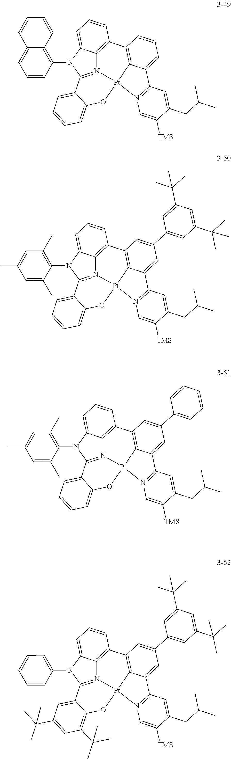
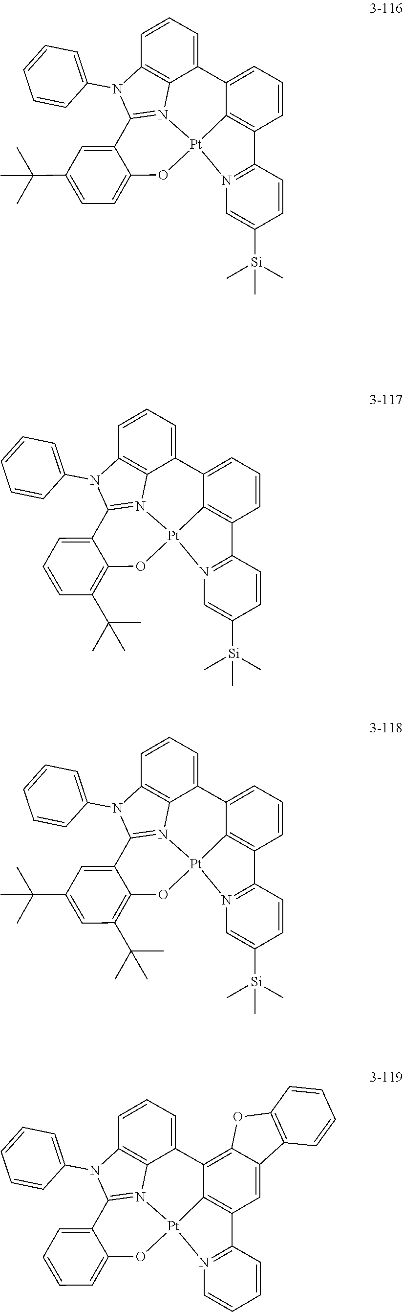
For example, the dopant may be one of Compounds 1-1 to 1-88, 2-1 to 2-47, and 3-1 to 3-582, but embodiments of the present disclosure are not limited thereto:
Figure US10692417-20200623-C00009
Figure US10692417-20200623-C00010
Figure US10692417-20200623-C00011
Figure US10692417-20200623-C00012
Figure US10692417-20200623-C00013
Figure US10692417-20200623-C00014
Figure US10692417-20200623-C00015
Figure US10692417-20200623-C00016
Figure US10692417-20200623-C00017
Figure US10692417-20200623-C00018
Figure US10692417-20200623-C00019
Figure US10692417-20200623-C00020
Figure US10692417-20200623-C00021
Figure US10692417-20200623-C00022
Figure US10692417-20200623-C00023
Figure US10692417-20200623-C00024
Figure US10692417-20200623-C00025
Figure US10692417-20200623-C00026
Figure US10692417-20200623-C00027
Figure US10692417-20200623-C00028
Figure US10692417-20200623-C00029
Figure US10692417-20200623-C00030
Figure US10692417-20200623-C00031
Figure US10692417-20200623-C00032
Figure US10692417-20200623-C00033
Figure US10692417-20200623-C00034
Figure US10692417-20200623-C00035
Figure US10692417-20200623-C00036
Figure US10692417-20200623-C00037
Figure US10692417-20200623-C00038
Figure US10692417-20200623-C00039
Figure US10692417-20200623-C00040
Figure US10692417-20200623-C00041
Figure US10692417-20200623-C00042
Figure US10692417-20200623-C00043
Figure US10692417-20200623-C00044
Figure US10692417-20200623-C00045
Figure US10692417-20200623-C00046
Figure US10692417-20200623-C00047
Figure US10692417-20200623-C00048
Figure US10692417-20200623-C00049
Figure US10692417-20200623-C00050
Figure US10692417-20200623-C00051
Figure US10692417-20200623-C00052
Figure US10692417-20200623-C00053
Figure US10692417-20200623-C00054
Figure US10692417-20200623-C00055
Figure US10692417-20200623-C00056
Figure US10692417-20200623-C00057
Figure US10692417-20200623-C00058
Figure US10692417-20200623-C00059
Figure US10692417-20200623-C00060
Figure US10692417-20200623-C00061
Figure US10692417-20200623-C00062
Figure US10692417-20200623-C00063
Figure US10692417-20200623-C00064
Figure US10692417-20200623-C00065
Figure US10692417-20200623-C00066
Figure US10692417-20200623-C00067
Figure US10692417-20200623-C00068
Figure US10692417-20200623-C00069
Figure US10692417-20200623-C00070
Figure US10692417-20200623-C00071
Figure US10692417-20200623-C00072
Figure US10692417-20200623-C00073
Figure US10692417-20200623-C00074
Figure US10692417-20200623-C00075
Figure US10692417-20200623-C00076
Figure US10692417-20200623-C00077
Figure US10692417-20200623-C00078
Figure US10692417-20200623-C00079
Figure US10692417-20200623-C00080
Figure US10692417-20200623-C00081
Figure US10692417-20200623-C00082
Figure US10692417-20200623-C00083
Figure US10692417-20200623-C00084
Figure US10692417-20200623-C00085
Figure US10692417-20200623-C00086
Figure US10692417-20200623-C00087
Figure US10692417-20200623-C00088
Figure US10692417-20200623-C00089
Figure US10692417-20200623-C00090
Figure US10692417-20200623-C00091
Figure US10692417-20200623-C00092
Figure US10692417-20200623-C00093
Figure US10692417-20200623-C00094
Figure US10692417-20200623-C00095
Figure US10692417-20200623-C00096
Figure US10692417-20200623-C00097
Figure US10692417-20200623-C00098
Figure US10692417-20200623-C00099
Figure US10692417-20200623-C00100
Figure US10692417-20200623-C00101
Figure US10692417-20200623-C00102
Figure US10692417-20200623-C00103
Figure US10692417-20200623-C00104
Figure US10692417-20200623-C00105
Figure US10692417-20200623-C00106
Figure US10692417-20200623-C00107
Figure US10692417-20200623-C00108
Figure US10692417-20200623-C00109
Figure US10692417-20200623-C00110
Figure US10692417-20200623-C00111
Figure US10692417-20200623-C00112
Figure US10692417-20200623-C00113
Figure US10692417-20200623-C00114
Figure US10692417-20200623-C00115
Figure US10692417-20200623-C00116
Figure US10692417-20200623-C00117
Figure US10692417-20200623-C00118
Figure US10692417-20200623-C00119
Figure US10692417-20200623-C00120
Figure US10692417-20200623-C00121
Figure US10692417-20200623-C00122
Figure US10692417-20200623-C00123
Figure US10692417-20200623-C00124
Figure US10692417-20200623-C00125
Figure US10692417-20200623-C00126
Figure US10692417-20200623-C00127
Figure US10692417-20200623-C00128
Figure US10692417-20200623-C00129
Figure US10692417-20200623-C00130
Figure US10692417-20200623-C00131
Figure US10692417-20200623-C00132
Figure US10692417-20200623-C00133
Figure US10692417-20200623-C00134
Figure US10692417-20200623-C00135
Figure US10692417-20200623-C00136
Figure US10692417-20200623-C00137
Figure US10692417-20200623-C00138
Figure US10692417-20200623-C00139
Figure US10692417-20200623-C00140
Figure US10692417-20200623-C00141
Figure US10692417-20200623-C00142
Figure US10692417-20200623-C00143
Figure US10692417-20200623-C00144
Figure US10692417-20200623-C00145
Figure US10692417-20200623-C00146
Figure US10692417-20200623-C00147
Figure US10692417-20200623-C00148
Figure US10692417-20200623-C00149
Figure US10692417-20200623-C00150
Figure US10692417-20200623-C00151
Figure US10692417-20200623-C00152
Figure US10692417-20200623-C00153
Figure US10692417-20200623-C00154
Figure US10692417-20200623-C00155
Figure US10692417-20200623-C00156
Figure US10692417-20200623-C00157
Although the above description mainly discuses an embodiment in which the emission layer of the green light-emitting unit (green OLED) 30 includes a phosphorescent light-emitting material, the present disclosure is not limited thereto. The emission layer of the green light-emitting unit (green OLED) 30 may include a thermally activated delayed fluorescence (TADF) dopant. The TADF dopant may be referred to as the thermally assisted delayed fluorescence dopant. In this case, high efficient delayed fluorescence emission may be possible.
Although the emission layer of the green light-emitting unit (green OLED) 30 may include the above-described phosphorescent light-emitting material, the present disclosure is not limited thereto. The emission layer may include a different phosphorescent material other than the above-described phosphorescent light-emitting material. Furthermore, the emission layer of the green light-emitting unit 30 may include a fluorescent light-emitting material. All green fluorescent materials used for OLEDs according to the related art may be applied to the green emission layer material according to the present disclosure. Since the fluorescent light-emitting material to emit a green light is well-known, a detailed description thereof is omitted.
In the present embodiment, the emission layer of the first and second blue light-emitting units 20 and 40 may include a fluorescent light-emitting material and/or a phosphorescent light-emitting material to emit a blue light. All blue fluorescent/phosphorescent materials used in the OLEDs according to the related art may be used as the blue emission layer material according to the present disclosure. Since the fluorescent light-emitting material and phosphorescent light-emitting material to emit a blue light are well-known, a detailed description thereof is omitted.
FIG. 12 is a graph showing a photoluminescence (PL) quantum yield (percent, %) according to the wavelengths of a Green-QD containing color converter and a Red-QD containing color converter that are applicable to a display apparatus according to an embodiment.
Referring to FIG. 12, it may be seen that the Green-QD containing color converter shows a PL quantum yield approximately to the green wavelength range and the Red-QD containing color converter shows a PL quantum yield approximately to the red wavelength range. The Green-QD containing color converter and the Red-QD containing color converter may be applied to the first color control element 70 a and the second color control element 70 b of FIG. 1, respectively.
FIG. 13 is a graph showing a change in the transmittance (%) according to the wavelengths of a Green-QD containing color converter and a Red-QD containing color converter that are applicable to a display apparatus according to an embodiment.
Referring to FIG. 13, it may be seen that the Green-QD containing color converter shows a high transmittance from a wavelength approximately corresponding to the green range and the Red-QD containing color converter shows a high transmittance from a wavelength approximately corresponding to the red range.
FIG. 14 is a graph showing the emission spectrum of an OLED substrate (light source) that is applicable to a display apparatus according to an embodiment. The OLED substrate (light source) corresponds to the OLED substrate 100 of FIG. 1 or the OLED substrate 101 of FIG. 9, and is configured to emit a mixed light of a blue light and a green light.
Referring to FIG. 14, it may be seen that the OLED substrate (light source) according to an embodiment mainly emits lights in a blue wavelength range and the green wavelength range, and a light corresponding to an intermediate area between the blue wavelength range and the green wavelength range.
FIG. 15 is a graph showing the emission spectrum of a light that is emitted from an OLED substrate (light source) and then passes through a Green-QD containing color converter, according to an embodiment. As illustrated in FIG. 15, it may be seen that, after the light generated from the OLED substrate (light source) passes through the Green-QD containing color converter, the light in the green wavelength range is strengthened. Although the light in blue wavelength range may be partially left, the remaining blue light may be blocked by the first color filter 80 a of FIG. 1.
FIG. 16 is a graph showing the emission spectrum of a light that is emitted from the OLED substrate (light source) and then passes through a Red-QD containing color converter, according to an embodiment. As illustrated in FIG. 16, it may be seen that, after the light generated from the OLED substrate (light source) passes through the Red-QD containing color converter, the light of the red wavelength range is strengthened. Although the lights in the blue wavelength range and the green wavelength range are partially left, the remaining blue light and green light may be blocked by the second color filter 80 b of FIG. 1.
FIG. 17 is a graph showing a change in transmittance (%) according to the wavelength of an absorption type color filter that is applicable to a display apparatus according to an embodiment. FIG. 17 includes the result of each of an absorption type Red-color filter, an absorption type Green-color filter, and an absorption type Blue-color filter. The absorption type Green-color filter, the absorption type Red-color filter, and the absorption type Blue-color filter may be applied to, for example, the first color filter 75 a, the second color filter 75 b, and the third color filter (third color control element) 75 c of FIG. 4, respectively.
FIG. 18 is a graph showing a change in transmittance (%) according to the wavelength of a cut-off type color filter that is applicable to a display apparatus according to an embodiment. FIG. 18 includes the results of each of a cut-off Red-color filter, a cut-off Green-color filter, and a cut-off Blue-color filter. The cut-off Green-color filter, the cut-off Red-color filter, and the cut-off Blue-color filter may be applied to, for example, the first color filter 80 a, the second color filter 80 b, and the third color filter 80 c of FIG. 3, respectively.
FIG. 19 is a graph showing a change in transmittance (%) according to the wavelength of an absorption type color filter that is applicable to a display apparatus according to an embodiment. FIG. 19 illustrates the results of each of an absorption type Red-color filter (CF-Red), an absorption type Green-color filter (CF-Green), and an absorption type Blue-color filter (CF-Blue). Furthermore, FIG. 19 includes the results of each of an absorption type low-reflection Red-color filter (low-reflection R), an absorption type low-reflection Green-color filter (low-reflection G), and an absorption type low-reflection Blue-color filter (low-reflection B). In the absorption type low-reflection Red-color filter, the expression “low-reflection” means that the reflectance of the absorption type low-reflection Red-color filter is relatively lower than that of the absorption type Red-color filter. This applied to the absorption type low-reflection Green-color filter and the absorption type low-reflection Blue-color filter. The reflectance and transmittance thereof may be appropriately adjusted by controlling the configuration of a color filter. The above-described absorption type low-reflection Green-color filter, absorption type low-reflection Red-color filter, and absorption type low-reflection Blue-color filter may also be applied to the first color filter 75 a, the second color filter 75 b, and the third color filter (third color control element) 75 c of FIG. 4, respectively. Since reflectivity of a panel may be reduced by using an absorption type low-reflection color filter, a contrast ratio may be increased without a circular polarizer.
FIG. 20 is a graph showing a difference in the spectral radiance between an embodiment in which the light scattering agent is used with respect to a blue light and an embodiment in which the light scattering agent is not used with respect to the blue light.
Referring to FIG. 20, it may be seen that, when the light scattering agent is not used (Before scattering agent), light is not dispersed well and thus a lot of peaks are generated. When the light scattering agent is used (After scattering agent), it may be seen that light is dispersed well, and thus one peak having a relatively smooth curve is generated.
FIG. 21 is a graph showing a change in current efficiency (candelas per Ampere, cd/A) according to various conditions with regard to a display apparatus.
Referring to FIG. 21, the last one of various conditions on an X-axis is a “B/G/B_QD CF” condition corresponding to the present embodiment. This is an embodiment in which the display apparatus includes a plurality of color filters (color controllers) formed of QDs and the OLED light source of a B/G/B tandem structure. Among the conditions on the X-axis, “B/Y/B_QD CF” and “B/RY/B_QD CF” are cases of using a white OLED light source, and “B/B/B_QD CF” and “B/B_QD CF” are cases of using a blue OLED light source.
It may be seen from the result of FIG. 21 that, when a display apparatus is configured based on the “B/G/B_QD CF” condition corresponding to the present embodiment, the highest current efficiency can be obtained. For the “B/G/B_QD CF” condition, the current efficiency appears to be higher than 11 cd/A, and for “B/B/B_QD CF” condition, the current efficiency is about 10 cd/A. A difference in the efficiency therebetween may be 10% or more. In particular, since in the “B/B_QD CF” condition the current efficiency is about 7.5 cd/A, the current efficiency of the “B/G/B_QD CF” condition may have a value that is 1.5 times greater than the value of the “B/B_QD CF” condition. Accordingly, when a display apparatus is formed based on the condition according to an embodiment, a high current efficiency may be obtained.
FIG. 22 is a graph showing a change in color characteristics (%) according to various conditions with regard to a display apparatus. The conditions corresponding to an X-axis of FIG. 22 may be the same as or similar to the conditions described with reference to FIG. 21. FIG. 22 includes a value measured based on the DCI_Gamut and a value measured based on the DCI_Coverage.
Referring to FIG. 22, color characteristics (%) values based on the DCI_Coverage under the conditions of “B/Y/B_QD CF”, “B/RY/B_QD CF”, “B/B/B_QD CF”, and “B/B_QD CF” according to comparative examples are almost the same. However, the color characteristics value based on the “B/G/B_QD CF” condition according to an embodiment may be higher than the values according to the comparative examples. Furthermore, the color characteristics (%) based on DCI_Gamut may have the highest color characteristics value under “B/G/B_QD CF” condition according to an embodiment. Accordingly, when a display apparatus is formed based on the condition according to an embodiment, excellent color characteristics and color gamut may be obtained.
The display apparatuses according to the above-described embodiments may be applied to a variety of electronic apparatuses. For example, the display apparatuses according to the above-described embodiments may be applied to small electronic apparatuses such as portable apparatuses or wearable apparatuses and to medium- and large-sized electronic apparatuses such as home appliances.
It should be understood that embodiments described herein should be considered in a descriptive sense only and not for purposes of limitation. Descriptions of features or aspects within each embodiment should typically be considered as available for other similar features or aspects in other embodiments. Those skilled in the art will appreciate that the configuration of and the connection between the OLED substrates, the color controllers, and the display apparatus including the same described with reference to FIGS. 1 to 11 can be modified in a variety of ways. While one or more embodiments have been described with reference to the figures, it will be understood by those of ordinary skill in the art that various changes in form and details may be made therein without departing from the spirit and scope of the present description as defined by the following claims.

Claims (23)

What is claimed is:
1. A display apparatus comprising:
an OLED (organic light-emitting device) substrate comprising a structure in which at least one blue light-emitting unit and at least one green light-emitting unit are stacked, wherein the OLED substrate generates a mixed light of a blue light and a green light; and
a color controller provided on the OLED substrate to adjust color of a light generated from the OLED substrate,
wherein the color controller comprises:
a first color control element comprising a plurality of first quantum dots for green conversion;
a second color control element comprising a plurality of second quantum dots for red conversion;
a third color control element for presenting a blue color;
a first color filter provided on the first color control element; and
a second color filter provided on the second color control element.
2. The display apparatus of claim 1, wherein the OLED substrate has a tandem structure.
3. The display apparatus of claim 1, wherein
the OLED substrate comprises a first blue light-emitting unit, a green light-emitting unit, and a second blue light-emitting unit which are sequentially stacked, and
the green light-emitting unit is arranged between the first and second blue light-emitting units.
4. The display apparatus of claim 3, further comprising:
a first charge generation layer provided between the first blue light-emitting unit and the green light-emitting unit; and
a second charge generation layer provided between the green light-emitting unit and the second blue light-emitting unit.
5. The display apparatus of claim 1, wherein
the green light-emitting unit comprises a green emission layer comprising an organic material, and
the green emission layer comprises a thermally activated delayed fluorescence (TADF) dopant.
6. The display apparatus of claim 1, wherein
the green light-emitting unit comprises a green emission layer comprising an organic material,
the green emission layer comprises a phosphorescent dopant, and
the phosphorescent dopant satisfies T1 (dopant)≤S1 (dopant)≤T1 (dopant)+0.5 electron Volts, wherein the T1 (dopant) is a triplet energy level (expressed in electron Volts) of the dopant and the S1 (dopant) is a singlet energy level (expressed in electron Volts) of the dopant.
7. The display apparatus of claim 6, wherein the dopant is an organic metal compound containing iridium (Ir).
8. The display apparatus of claim 6, wherein the dopant is an organic metal compound containing at least one of platinum (Pt), osmium (Os), titanium (Ti), zirconium (Zr), hafnium (Hf), europium (Eu), terbium (Tb), thulium (Tm), rhodium (Rh), ruthenium (Ru), rhenium (Re), beryllium (Be), magnesium (Mg), aluminum (Al), calcium (Ca), manganese (Mn), cobalt (Co), copper (Cu), zinc (Zn), gallium (Ga), germanium (Ge), palladium (Pd), silver (Ag), and gold (Au).
9. The display apparatus of claim 6, wherein the dopant is an organic metal compound having a square-planar coordination structure.
10. The display apparatus of claim 6, wherein
the dopant comprises a metal M and an organic ligand, and
the metal M and the organic ligand form one, two, or three cyclometallated rings.
11. The display apparatus of claim 6, wherein
the dopant comprises a metal M and a four-coordinate organic ligand that forms three or four cyclometallated rings,
the metal M comprises platinum (Pt), osmium (Os), titanium (Ti), zirconium (Zr), hafnium (Hf), europium (Eu), terbium (Tb), thulium (Tm), rhodium (Rh), ruthenium (Ru), rhenium (Re), beryllium (Be), magnesium (Mg), aluminum (Al), calcium (Ca), manganese (Mn), cobalt (Co), copper (Cu), zinc (Zn), gallium (Ga), germanium (Ge), palladium (Pd), silver (Ag), or gold (Au), and
the four-coordinate organic ligand comprises a benzimidazole group or a pyridine group.
12. The display apparatus of claim 1, wherein
the first color filter is a blue cut filter, and
the second color filter is a blue and green cut filter.
13. The display apparatus of claim 1, wherein
the first color filter is an absorption type green color filter, and
the second color filter is an absorption type red color filter.
14. The display apparatus of claim 1, wherein
the third color control element comprises a blue color filter, and
the display apparatus further comprises a light scattering element provided between the blue color filter and the OLED substrate.
15. The display apparatus of claim 1, wherein
the third color control element comprises a color converter comprising a plurality of third quantum dots for blue conversion, and
the display apparatus further comprises a third color filter provided on the third color control element.
16. The display apparatus of claim 15, wherein the third color filter is a green cut filter or an absorption type blue color filter.
17. The display apparatus of claim 1, wherein a core part of the second quantum dot has a size greater than a core part of the first quantum dot.
18. The display apparatus of claim 1, wherein
the first color control element corresponds to a first sub-pixel area, the second color control element corresponds to a second sub-pixel area, and the third color control element corresponds to a third sub-pixel area, and
the display apparatus further comprises a fourth sub-pixel area, wherein the fourth sub-pixel area produces a color other than colors of the first to third sub-pixel areas.
19. The display apparatus of claim 18, wherein
the fourth sub-pixel area is a blank area on the OLED substrate without a color control element, or
the display apparatus comprises a light scattering element provided on the OLED substrate.
20. The display apparatus of claim 1, further comprising a selective reflection film provided between the OLED substrate and the color controller.
21. The display apparatus of claim 20, wherein the selective reflection film is configured to transmit a blue light and a green light and to reflect a red light.
22. The display apparatus of claim 1, further comprising a thin film transistor (TFT) array substrate having a plurality of thin film transistors to drive pixel areas of the OLED substrate.
23. An electronic apparatus comprising the display apparatus of claim 1.
US16/015,359 2017-06-23 2018-06-22 Display apparatus Active 2038-12-14 US10692417B2 (en)

Priority Applications (2)

Application Number Priority Date Filing Date Title
US16/857,693 US11562678B2 (en) 2017-06-23 2020-04-24 Display apparatus
US17/936,900 US11688322B2 (en) 2017-06-23 2022-09-30 Display apparatus

Applications Claiming Priority (4)

Application Number Priority Date Filing Date Title
KR10-2017-0079958 2017-06-23
KR20170079958 2017-06-23
KR10-2017-0116255 2017-09-12
KR1020170116255A KR102477097B1 (en) 2017-06-23 2017-09-12 Display apparatus

Related Child Applications (1)

Application Number Title Priority Date Filing Date
US16/857,693 Continuation US11562678B2 (en) 2017-06-23 2020-04-24 Display apparatus

Publications (2)

Publication Number Publication Date
US20180374409A1 US20180374409A1 (en) 2018-12-27
US10692417B2 true US10692417B2 (en) 2020-06-23

Family

ID=64692742

Family Applications (3)

Application Number Title Priority Date Filing Date
US16/015,359 Active 2038-12-14 US10692417B2 (en) 2017-06-23 2018-06-22 Display apparatus
US16/857,693 Active US11562678B2 (en) 2017-06-23 2020-04-24 Display apparatus
US17/936,900 Active US11688322B2 (en) 2017-06-23 2022-09-30 Display apparatus

Family Applications After (2)

Application Number Title Priority Date Filing Date
US16/857,693 Active US11562678B2 (en) 2017-06-23 2020-04-24 Display apparatus
US17/936,900 Active US11688322B2 (en) 2017-06-23 2022-09-30 Display apparatus

Country Status (2)

Country Link
US (3) US10692417B2 (en)
KR (1) KR102520859B1 (en)

Cited By (9)

* Cited by examiner, † Cited by third party
Publication number Priority date Publication date Assignee Title
US10964757B2 (en) 2018-07-25 2021-03-30 Universal Display Corporation Energy efficient OLED TV
US20210253618A1 (en) * 2020-02-10 2021-08-19 Samsung Electronics Co., Ltd. Organometallic compound, organic light-emitting device including the same, and electronic apparatus including the organic light-emitting device
US11271050B2 (en) * 2017-11-21 2022-03-08 Samsung Electronics Co., Ltd. Color control encapsulation layer and display apparatus including the same
US11562678B2 (en) * 2017-06-23 2023-01-24 Samsung Electronics Co., Ltd. Display apparatus
US12219786B2 (en) 2020-11-12 2025-02-04 Samsung Display Co., Ltd. Display apparatus
US12225800B2 (en) 2021-03-04 2025-02-11 Samsung Electronics Co., Ltd. Display panel and electronic device including the same
US12274123B2 (en) 2021-04-05 2025-04-08 Samsung Display Co., Ltd. Light emitting device and display apparatus including the same
US12501811B2 (en) 2022-03-30 2025-12-16 Samsung Display Co., Ltd. Light emitting display device that includes color filter layer and quantum dot layer
US12510814B1 (en) 2021-12-23 2025-12-30 The Invisible Pixel Inc. Projection system and methods therefor

Families Citing this family (31)

* Cited by examiner, † Cited by third party
Publication number Priority date Publication date Assignee Title
US11793010B2 (en) * 2018-06-06 2023-10-17 Semiconductor Energy Laboratory Co., Ltd. Display device, display module, and electronic device
CN109065740A (en) * 2018-08-10 2018-12-21 京东方科技集团股份有限公司 Oled display substrate and preparation method thereof, display device
KR102285669B1 (en) * 2018-08-27 2021-08-04 동우 화인켐 주식회사 A color filter, a method of making thereof, and an image display device comprising thereof
CN109841755A (en) * 2019-03-08 2019-06-04 深圳市华星光电半导体显示技术有限公司 Production method, display panel and the electronic equipment of display panel
CN110021652A (en) * 2019-04-03 2019-07-16 深圳市华星光电半导体显示技术有限公司 Quantum dot flexibility OLED display and preparation method
CN110071144A (en) * 2019-04-08 2019-07-30 深圳市华星光电半导体显示技术有限公司 OLED display and preparation method
KR102325381B1 (en) * 2019-04-15 2021-11-10 삼성디스플레이 주식회사 Display device
US11839093B2 (en) * 2019-05-14 2023-12-05 Kopin Corporation Image rendering in organic light emitting diode (OLED) displays, apparatuses, systems, and methods
US20200373360A1 (en) * 2019-05-23 2020-11-26 Universal Display Corporation Oled display panel with unpatterned emissive stack
WO2021024337A1 (en) * 2019-08-05 2021-02-11 シャープ株式会社 Display device and method for producing display device
KR102760407B1 (en) 2019-09-04 2025-02-04 삼성디스플레이 주식회사 Organic light emitting diode and display device having the same
US11502136B2 (en) 2019-11-11 2022-11-15 Samsung Display Co., Ltd. Display panel
KR102773495B1 (en) * 2020-02-10 2025-02-28 삼성디스플레이 주식회사 Organic light emitting device
KR20210116730A (en) * 2020-03-12 2021-09-28 삼성디스플레이 주식회사 Display apparatus and method of manufacturing the same
WO2021192157A1 (en) * 2020-03-26 2021-09-30 シャープ株式会社 Light-emitting element, and display device
KR102333517B1 (en) * 2020-06-24 2021-12-01 삼성디스플레이 주식회사 Display device
KR102853006B1 (en) * 2020-06-26 2025-08-29 엘지디스플레이 주식회사 Display device
GB202010090D0 (en) * 2020-07-01 2020-08-12 Savvy Science Improved light emitting devices
KR20220037716A (en) 2020-09-18 2022-03-25 삼성전자주식회사 Display apparatus
KR20220080803A (en) * 2020-12-07 2022-06-15 삼성디스플레이 주식회사 Light emitting device and electronic apparatus comprising same
US12256621B2 (en) 2021-03-05 2025-03-18 Samsung Electronics Co., Ltd. Display panel and electronic device including the same
CN113629206A (en) * 2021-07-20 2021-11-09 武汉华星光电半导体显示技术有限公司 Display panel and display device
KR20230023123A (en) 2021-08-09 2023-02-17 삼성디스플레이 주식회사 Light emitting device and electronic apparatus comprising same
KR102760051B1 (en) * 2021-09-16 2025-01-24 삼성전자주식회사 Light emitting device and electronic apparatus including the same
KR20230098395A (en) * 2021-12-24 2023-07-04 삼성디스플레이 주식회사 Optical member and display panel
KR20230101989A (en) * 2021-12-29 2023-07-07 삼성디스플레이 주식회사 Substrate including light emitting diodes and display device including the same
KR20230158167A (en) * 2022-05-10 2023-11-20 삼성디스플레이 주식회사 Display device
US20240268135A1 (en) * 2022-06-29 2024-08-08 Boe Technology Group Co., Ltd. Light emitting device, light emitting base plate and light emitting apparatus
KR20240019644A (en) 2022-08-04 2024-02-14 삼성전자주식회사 Display apparatus
KR20240019643A (en) 2022-08-04 2024-02-14 삼성전자주식회사 Display apparatus
CN117642008A (en) * 2022-08-29 2024-03-01 三星电子株式会社 Display panel and electronic device including the display panel

Citations (17)

* Cited by examiner, † Cited by third party
Publication number Priority date Publication date Assignee Title
US20040251821A1 (en) * 2003-06-11 2004-12-16 Eastman Kodak Company Stacked OLED display having improved efficiency
US20060221021A1 (en) * 2005-04-01 2006-10-05 Hajjar Roger A Display systems having screens with optical fluorescent materials
US20070014318A1 (en) * 2005-04-01 2007-01-18 Hajjar Roger A Display screens having optical fluorescent materials
US20100149815A1 (en) * 2008-10-17 2010-06-17 Luminus Devices, Inc. Remote lighting assemblies and methods
US20120287148A1 (en) * 2011-05-13 2012-11-15 Candice Hellen Brown Elliott Method and apparatus for improved subpixel rendering
US20130215360A1 (en) * 2011-05-13 2013-08-22 Samsung Display Co., Ltd. Method for reducing simultaneous contrast error
US9046227B2 (en) * 2009-09-18 2015-06-02 Soraa, Inc. LED lamps with improved quality of light
US9064822B2 (en) 2013-10-10 2015-06-23 Lg Display Co., Ltd. Organic electroluminescent device and method of manufacturing the same
US20150185381A1 (en) 2013-12-26 2015-07-02 Ye Xin Technology Consulting Co., Ltd. Display device with color conversion layer for full-color display
US20150228697A1 (en) 2013-09-12 2015-08-13 Shenzhen China Star Optoelectronics Technology Co., Ltd. Organic light emitting diode (oled) device and a method of fabricating the same
US20150318506A1 (en) 2013-04-23 2015-11-05 Boe Technology Group Co., Ltd. Organic light emitting diode display apparatus
JP2016122606A (en) 2014-12-25 2016-07-07 シャープ株式会社 Wavelength conversion system light-emitting device and display device including the same, lighting system and electronic apparatus
KR101686715B1 (en) 2014-12-24 2016-12-14 엘지전자 주식회사 Display device
US20170017123A1 (en) 2015-07-14 2017-01-19 Samsung Electronics Co., Ltd. Display panel and a displaying apparatus using the same
US20170110043A1 (en) * 2015-05-29 2017-04-20 Boe Technology Group Co., Ltd. Field sequential display panel, field sequential display device and driving method
US20180019371A1 (en) * 2016-03-17 2018-01-18 Apple Inc. Quantum dot spacing for high efficiency quantum dot led displays
US20180188599A1 (en) * 2016-04-11 2018-07-05 Boe Technology Group., Ltd. Display device

Family Cites Families (9)

* Cited by examiner, † Cited by third party
Publication number Priority date Publication date Assignee Title
CN101924190B (en) * 2000-08-11 2012-07-04 普林斯顿大学理事会 Organometallic compounds and emission-shifting organic electrophosphorescence
KR101407574B1 (en) 2007-01-12 2014-06-17 삼성디스플레이 주식회사 White light emitting device
DE102008057051B4 (en) * 2008-11-13 2021-06-17 Merck Patent Gmbh Materials for organic electroluminescent devices
KR20150126381A (en) 2013-04-05 2015-11-11 코니카 미놀타 가부시키가이샤 Coating liquid for forming light emitting layer, organic electroluminescent element, method for manufacturing organic electroluminescent element, and lighting/display device
JPWO2015147073A1 (en) * 2014-03-25 2017-04-13 コニカミノルタ株式会社 ORGANIC ELECTROLUMINESCENT ELEMENT AND LIGHTING DEVICE
KR20160000811A (en) 2014-06-24 2016-01-05 엘지디스플레이 주식회사 Organic Light Emitting Device
JP5918340B2 (en) 2014-11-25 2016-05-18 ユー・ディー・シー アイルランド リミテッド Color display device and manufacturing method thereof
KR102745472B1 (en) * 2016-11-23 2024-12-20 엘지디스플레이 주식회사 Organic Light Emitting Element and Organic Light Emitting Display Device
US10692417B2 (en) * 2017-06-23 2020-06-23 Samsung Electronic Co., Ltd. Display apparatus

Patent Citations (19)

* Cited by examiner, † Cited by third party
Publication number Priority date Publication date Assignee Title
US20040251821A1 (en) * 2003-06-11 2004-12-16 Eastman Kodak Company Stacked OLED display having improved efficiency
US20060221021A1 (en) * 2005-04-01 2006-10-05 Hajjar Roger A Display systems having screens with optical fluorescent materials
US20070014318A1 (en) * 2005-04-01 2007-01-18 Hajjar Roger A Display screens having optical fluorescent materials
US20100149815A1 (en) * 2008-10-17 2010-06-17 Luminus Devices, Inc. Remote lighting assemblies and methods
US9046227B2 (en) * 2009-09-18 2015-06-02 Soraa, Inc. LED lamps with improved quality of light
US20120287148A1 (en) * 2011-05-13 2012-11-15 Candice Hellen Brown Elliott Method and apparatus for improved subpixel rendering
US20130215360A1 (en) * 2011-05-13 2013-08-22 Samsung Display Co., Ltd. Method for reducing simultaneous contrast error
US20150318506A1 (en) 2013-04-23 2015-11-05 Boe Technology Group Co., Ltd. Organic light emitting diode display apparatus
US20150228697A1 (en) 2013-09-12 2015-08-13 Shenzhen China Star Optoelectronics Technology Co., Ltd. Organic light emitting diode (oled) device and a method of fabricating the same
US9064822B2 (en) 2013-10-10 2015-06-23 Lg Display Co., Ltd. Organic electroluminescent device and method of manufacturing the same
US20150185381A1 (en) 2013-12-26 2015-07-02 Ye Xin Technology Consulting Co., Ltd. Display device with color conversion layer for full-color display
KR101686715B1 (en) 2014-12-24 2016-12-14 엘지전자 주식회사 Display device
US20170352714A1 (en) 2014-12-24 2017-12-07 Lg Electronics Inc. Display device
JP2016122606A (en) 2014-12-25 2016-07-07 シャープ株式会社 Wavelength conversion system light-emitting device and display device including the same, lighting system and electronic apparatus
US20170110043A1 (en) * 2015-05-29 2017-04-20 Boe Technology Group Co., Ltd. Field sequential display panel, field sequential display device and driving method
US20170017123A1 (en) 2015-07-14 2017-01-19 Samsung Electronics Co., Ltd. Display panel and a displaying apparatus using the same
KR20170008591A (en) 2015-07-14 2017-01-24 삼성전자주식회사 A display assembly and a displaying apparatus using the same
US20180019371A1 (en) * 2016-03-17 2018-01-18 Apple Inc. Quantum dot spacing for high efficiency quantum dot led displays
US20180188599A1 (en) * 2016-04-11 2018-07-05 Boe Technology Group., Ltd. Display device

Cited By (15)

* Cited by examiner, † Cited by third party
Publication number Priority date Publication date Assignee Title
US11688322B2 (en) 2017-06-23 2023-06-27 Samsung Electronics Co., Ltd. Display apparatus
US11562678B2 (en) * 2017-06-23 2023-01-24 Samsung Electronics Co., Ltd. Display apparatus
US11672155B2 (en) 2017-11-21 2023-06-06 Samsung Electronics Co., Ltd. Color control encapsulation layer and display apparatus including the same
US11271050B2 (en) * 2017-11-21 2022-03-08 Samsung Electronics Co., Ltd. Color control encapsulation layer and display apparatus including the same
US11700756B2 (en) 2018-07-25 2023-07-11 Universal Display Corporation Energy efficient OLED TV
US10964757B2 (en) 2018-07-25 2021-03-30 Universal Display Corporation Energy efficient OLED TV
US11839124B2 (en) 2018-07-25 2023-12-05 Universal Display Corporation Energy efficient OLED TV
US12193300B2 (en) 2018-07-25 2025-01-07 Universal Display Corporation Organic electroluminescent devices
US20210253618A1 (en) * 2020-02-10 2021-08-19 Samsung Electronics Co., Ltd. Organometallic compound, organic light-emitting device including the same, and electronic apparatus including the organic light-emitting device
US12240863B2 (en) * 2020-02-10 2025-03-04 Samsung Electronics Co., Ltd. Organometallic compound, organic light-emitting device including the same, and electronic apparatus including the organic light-emitting device
US12219786B2 (en) 2020-11-12 2025-02-04 Samsung Display Co., Ltd. Display apparatus
US12225800B2 (en) 2021-03-04 2025-02-11 Samsung Electronics Co., Ltd. Display panel and electronic device including the same
US12274123B2 (en) 2021-04-05 2025-04-08 Samsung Display Co., Ltd. Light emitting device and display apparatus including the same
US12510814B1 (en) 2021-12-23 2025-12-30 The Invisible Pixel Inc. Projection system and methods therefor
US12501811B2 (en) 2022-03-30 2025-12-16 Samsung Display Co., Ltd. Light emitting display device that includes color filter layer and quantum dot layer

Also Published As

Publication number Publication date
US11688322B2 (en) 2023-06-27
US20200251040A1 (en) 2020-08-06
US20230064422A1 (en) 2023-03-02
KR102520859B1 (en) 2023-04-13
KR20220062256A (en) 2022-05-16
US11562678B2 (en) 2023-01-24
US20180374409A1 (en) 2018-12-27

Similar Documents

Publication Publication Date Title
US11688322B2 (en) Display apparatus
KR102477097B1 (en) Display apparatus
US12082490B2 (en) Light outcoupling efficiency of phosphorescent OLEDs by mixing horizontally aligned fluorescent emitters
KR102545346B1 (en) Top-emission printed displays with quantum dots and thermally activated delayed fluorescent molecules
KR102819737B1 (en) Purcell enhancement via tamm plasmon stack in oled structures
TW201838174A (en) Light emitting device and image display device using same
US20260033198A1 (en) Display apparatus
CN111615653A (en) Light-emitting element, display and color conversion substrate
JP2025031808A (en) Light-emitting device, electronic device and lighting device
KR20230048316A (en) Improved light emitting device
US20220131095A1 (en) Organometallic compound and an organic light-emitting device including the same
US20220052278A1 (en) Display apparatus
CN112552898A (en) Quantum dot composition, light emitting element, and display device including light emitting element
US20240381680A1 (en) Organic electroluminescent devices
US20230422599A1 (en) Organic electroluminescent materials and devices
CN114068832A (en) Light emitting device and electronic apparatus including the same
US20230165095A1 (en) Light-emitting device and electronic apparatus including the same
US20240180024A1 (en) Organic electroluminescent materials and devices
US20230337516A1 (en) Organic electroluminescent materials and devices
CN116267000A (en) Metal oxide composition, light emitting device and electronic device including light emitting device

Legal Events

Date Code Title Description
FEPP Fee payment procedure

Free format text: ENTITY STATUS SET TO UNDISCOUNTED (ORIGINAL EVENT CODE: BIG.); ENTITY STATUS OF PATENT OWNER: LARGE ENTITY

STPP Information on status: patent application and granting procedure in general

Free format text: DOCKETED NEW CASE - READY FOR EXAMINATION

STPP Information on status: patent application and granting procedure in general

Free format text: NOTICE OF ALLOWANCE MAILED -- APPLICATION RECEIVED IN OFFICE OF PUBLICATIONS

AS Assignment

Owner name: SAMSUNG ELECTRONICS CO., LTD., KOREA, REPUBLIC OF

Free format text: ASSIGNMENT OF ASSIGNORS INTEREST;ASSIGNORS:LEE, SANGYOON;LEE, SUNGHUN;JUN, SHINAE;AND OTHERS;REEL/FRAME:052377/0667

Effective date: 20180919

STPP Information on status: patent application and granting procedure in general

Free format text: PUBLICATIONS -- ISSUE FEE PAYMENT VERIFIED

STCF Information on status: patent grant

Free format text: PATENTED CASE

MAFP Maintenance fee payment

Free format text: PAYMENT OF MAINTENANCE FEE, 4TH YEAR, LARGE ENTITY (ORIGINAL EVENT CODE: M1551); ENTITY STATUS OF PATENT OWNER: LARGE ENTITY

Year of fee payment: 4