US10691189B2 - Line-voltage detection method, power controller and power supply with brown-out protection and brown-in mechanism - Google Patents
Line-voltage detection method, power controller and power supply with brown-out protection and brown-in mechanism Download PDFInfo
- Publication number
- US10691189B2 US10691189B2 US15/692,636 US201715692636A US10691189B2 US 10691189 B2 US10691189 B2 US 10691189B2 US 201715692636 A US201715692636 A US 201715692636A US 10691189 B2 US10691189 B2 US 10691189B2
- Authority
- US
- United States
- Prior art keywords
- voltage
- current
- line
- brown
- limiting resistor
- Prior art date
- Legal status (The legal status is an assumption and is not a legal conclusion. Google has not performed a legal analysis and makes no representation as to the accuracy of the status listed.)
- Active, expires
Links
Images


Classifications
-
- G—PHYSICS
- G06—COMPUTING OR CALCULATING; COUNTING
- G06F—ELECTRIC DIGITAL DATA PROCESSING
- G06F1/00—Details not covered by groups G06F3/00 - G06F13/00 and G06F21/00
- G06F1/26—Power supply means, e.g. regulation thereof
- G06F1/28—Supervision thereof, e.g. detecting power-supply failure by out of limits supervision
-
- G—PHYSICS
- G06—COMPUTING OR CALCULATING; COUNTING
- G06F—ELECTRIC DIGITAL DATA PROCESSING
- G06F1/00—Details not covered by groups G06F3/00 - G06F13/00 and G06F21/00
- G06F1/26—Power supply means, e.g. regulation thereof
- G06F1/30—Means for acting in the event of power-supply failure or interruption, e.g. power-supply fluctuations
- G06F1/305—Means for acting in the event of power-supply failure or interruption, e.g. power-supply fluctuations in the event of power-supply fluctuations
-
- H—ELECTRICITY
- H02—GENERATION; CONVERSION OR DISTRIBUTION OF ELECTRIC POWER
- H02H—EMERGENCY PROTECTIVE CIRCUIT ARRANGEMENTS
- H02H3/00—Emergency protective circuit arrangements for automatic disconnection directly responsive to an undesired change from normal electric working condition with or without subsequent reconnection ; integrated protection
- H02H3/20—Emergency protective circuit arrangements for automatic disconnection directly responsive to an undesired change from normal electric working condition with or without subsequent reconnection ; integrated protection responsive to excess voltage
- H02H3/207—Emergency protective circuit arrangements for automatic disconnection directly responsive to an undesired change from normal electric working condition with or without subsequent reconnection ; integrated protection responsive to excess voltage also responsive to under-voltage
-
- H—ELECTRICITY
- H02—GENERATION; CONVERSION OR DISTRIBUTION OF ELECTRIC POWER
- H02H—EMERGENCY PROTECTIVE CIRCUIT ARRANGEMENTS
- H02H3/00—Emergency protective circuit arrangements for automatic disconnection directly responsive to an undesired change from normal electric working condition with or without subsequent reconnection ; integrated protection
- H02H3/24—Emergency protective circuit arrangements for automatic disconnection directly responsive to an undesired change from normal electric working condition with or without subsequent reconnection ; integrated protection responsive to undervoltage or no-voltage
- H02H3/247—Emergency protective circuit arrangements for automatic disconnection directly responsive to an undesired change from normal electric working condition with or without subsequent reconnection ; integrated protection responsive to undervoltage or no-voltage having timing means
-
- H—ELECTRICITY
- H02—GENERATION; CONVERSION OR DISTRIBUTION OF ELECTRIC POWER
- H02H—EMERGENCY PROTECTIVE CIRCUIT ARRANGEMENTS
- H02H7/00—Emergency protective circuit arrangements specially adapted for specific types of electric machines or apparatus or for sectionalised protection of cable or line systems, and effecting automatic switching in the event of an undesired change from normal working conditions
- H02H7/10—Emergency protective circuit arrangements specially adapted for specific types of electric machines or apparatus or for sectionalised protection of cable or line systems, and effecting automatic switching in the event of an undesired change from normal working conditions for converters; for rectifiers
- H02H7/12—Emergency protective circuit arrangements specially adapted for specific types of electric machines or apparatus or for sectionalised protection of cable or line systems, and effecting automatic switching in the event of an undesired change from normal working conditions for converters; for rectifiers for static converters or rectifiers
- H02H7/122—Emergency protective circuit arrangements specially adapted for specific types of electric machines or apparatus or for sectionalised protection of cable or line systems, and effecting automatic switching in the event of an undesired change from normal working conditions for converters; for rectifiers for static converters or rectifiers for inverters, i.e. DC/AC converters
- H02H7/1222—Emergency protective circuit arrangements specially adapted for specific types of electric machines or apparatus or for sectionalised protection of cable or line systems, and effecting automatic switching in the event of an undesired change from normal working conditions for converters; for rectifiers for static converters or rectifiers for inverters, i.e. DC/AC converters responsive to abnormalities in the input circuit, e.g. transients in the DC input
Definitions
- the present disclosure relates generally to a line-voltage detection method for a power controller with high-voltage startup, and more particularly to brown-out protection and brown-in mechanism of a power controller with high-voltage startup.
- a line voltage normally refers to the voltage generated by rectifying an alternating-current (AC) voltage from a power grid, it is a direct-current voltage (DC), and its value always provides important information to AC-to-DC power supplies or converters.
- AC alternating-current
- DC direct-current voltage
- brown-out protection a power supply equipped with brown-in mechanism could resume its power conversion automatically and supply power to its load properly.
- awareness of the value of a line voltage could be used to compensate outcomes of a power supply that are otherwise influenced by the line voltage.
- FIG. 1 demonstrates an AC-to-DC power supply 100 with a flyback topology.
- Bridge rectifier 12 provides to an AC voltage V AC-MAIN from a power grid full-wave rectification to generate input voltage V IN at input node IN.
- Power controller 18 normally a packaged integrated circuit with pins, provides pulse-width modulation (PWM) signal S PWM to control power switch 26 , which in response controls a current flowing through transformer 16 .
- PWM pulse-width modulation
- Power controller 18 has a pin, named high-voltage node HV hereinafter, connected to line voltage V LINE via current-limiting resistor 20 .
- Power controller 18 is equipped with high-voltage startup technology. When AC-to-DC power supply 100 is just connected to the AC voltage V AC-MAIN , a high-voltage startup procedure commences, power controller 18 pulls a charging current from high-voltage node HV, this charging current is directed to go through operating voltage source node VCC and charge operating voltage capacitor 28 , so operating voltage V CC is built. Once operating voltage V CC is high or good enough, the high-voltage startup procedure concludes, the charging current stops, and power controller 18 starts providing PWM signal S PWM .
- FIG. 2A shows power controller 18 a that detects line voltage V LINE and is capable of performing brown-out protection.
- Power controller 18 a could replace power controller 18 , and has a high-voltage startup transistor 46 , which is turned ON during the high-voltage startup procedure to provide the charging current charging operating voltage capacitor 28 .
- voltage divider 40 a External to power controller 18 a , connected between high-voltage node HV and ground line GND is voltage divider 40 a consisting of resistors 42 a and 44 a .
- a joint node between resistors 42 a and 44 a is connected to sense node SENS of power controller 18 a and provides to power controller 18 a fraction result of line voltage V LINE .
- Brown-out reference means the reference voltage for line voltage V LINE to goes below and to trigger brown-out protection; brown-in reference means the reference voltage that line voltage V LINE must exceed to start brown-in mechanism.
- Another detection method for line voltage V LINE is to embed voltage divider 40 a of FIG. 2A in a power controller, as demonstrated by power controller 18 b in FIG. 2B .
- power controller 18 b in FIG. 2B has embedded voltage divider 40 b inside itself, and requires no pin for sense node SENS.
- a power supply based on power controller 18 b could be cheaper, but possibly in the expenses of the flexibility to the modification of brown-out and brown-in references. Power supply system designers could not change the brown-out and brown-in references for brown-out protection and brown-in mechanism once the power controller 18 b is fabricated.
- FIG. 1 demonstrates an AC-to-DC power supply with a flyback topology in the art
- FIGS. 2A and 2B shows two power controllers in the art
- FIG. 3 demonstrates a power controller according to embodiments of the invention
- FIG. 4 illustrates signal waveforms of signals in FIG. 3 ;
- FIG. 5 demonstrates another AC-to-DC power supply according to embodiments of the invention.
- FIG. 3 demonstrates a power controller 18 c according to embodiments of the invention.
- Power controller 18 c could be in form of a packaged integrated circuit and capable of replacing power controller 18 in FIG. 1 to provide PWM signal S PWM and control power switch 26 according to embodiments of the invention.
- high-voltage startup transistor 46 is connected to high-voltage node HV, which could be a pin of a packaged integrated circuit.
- high-voltage startup transistor 46 is a depletion-mode metal-oxide-semiconductor (MOS) transistor, or a depletion-mode junction field effect transistor (JFET), capable of sustaining a drain-to-source voltage more than 400V, or as high as 800V.
- MOS metal-oxide-semiconductor
- JFET depletion-mode junction field effect transistor
- Operating voltage source node VCC could be a pin of power controller 18 c if power controller 18 c is in form of an integrated circuit.
- operating voltage V CC exceeds a predetermined level, 20 volt for example, the high-voltage startup procedure concludes, high-voltage startup transistor 46 is turned OFF, probably because of the rise in the source voltage of the high-voltage startup transistor 46 , and the charging current stops.
- Operating voltage V CC is the power source that power controller 18 c relies on for normal operations.
- high-voltage startup transistor 46 has its drain connected to line voltage V LINE via high-voltage node HV and current-limiting resistor 20 .
- PWM signal S PWM could be generated to turn ON and OFF power switch 26 .
- Power controller 18 c includes controllable current source 206 , voltage divider 40 c , management circuit 204 , a brown-out protection circuit 208 , brown-in mechanism circuit 210 and signal generator 212 .
- Voltage divider 40 c includes two resistors 42 c and 44 c connected in series between high-voltage node HV and ground line GND. The joint between resistors 42 c and 44 c can feed fraction result V BNO of the input voltage V HV at high-voltage node HV to management circuit 204 , which in response controls controllable current source 206 .
- voltage divider 40 c divides input voltage V HV at high-voltage node HV to provide fraction result V BNO which is substantially in proportion to input voltage V HV .
- Management circuit 204 could turn ON controllable current source 206 , which accordingly pulls an offset current I OS , whose value is IOS, a positive number. Offset current I OS flows from line voltage V LINE , through current-limiting resistor 20 , high-voltage node HV, high-voltage startup transistor 46 , and controllable current source 206 , and to ground line GND. When controllable current source 206 is turned OFF, offset current I OS is about 0 A or disappears. Controllable current source 206 could be forbidden to be turned ON until a high-voltage startup procedure concludes or operating voltage V CC is high enough.
- management circuit 204 comprises comparator 220 , single pulse generator 222 , and control circuit 224 .
- Comparator 220 compares fraction result V BNO with a reference voltage V REF to generate a comparison result S CHK .
- Comparison result S CHK is “1” in logic if fraction result V BNO exceeds reference voltage V REF , or it is “0” in logic otherwise.
- comparison result S CHK turns from logic “0” into logic “1”
- control circuit 224 keeps controllable current source 206 OFF. Only if pulse signal S RES has logic value of “1”, can control circuit 224 allow clock signal CLK to turn ON controllable current source 206 .
- Single pulse generator 222 includes debouncing circuit 230 , NOT gate 234 , and AND gate 232 .
- Debouncing circuit 230 passes comparison result S CHK to be acknowledgement signal S BI if comparison result S CHK has been stable at “1” in logic for a predetermined debounce-time T DEB1 .
- acknowledgement signal S BI is “0” in logic if comparison result S CHK is “0” in logic.
- Acknowledgement signal S BI becomes “1” in logic only if comparison result S CHK has remained as “1” for debounce-time T DEB1 , which for example is about 300 us.
- NOT gate 234 and AND gate 232 together work as a logic circuit to generate pulse signal S RES in response to comparison result S CHK and acknowledgement single S BI .
- Control circuit 224 receives clock signal CLK and pulse signal S RES to control controllable current source 206 .
- pulse signal S RES does not exist, being “0” in logic
- D flip-flop 240 is reset all the time, keeping its output “0” in logic and turning controllable current source 206 OFF.
- pulse signal S RES occurs, being “1” in logic
- D flip-flop 240 which is then updated by a flowing rising edge of clock signal CLK, can turn controllable current source 206 ON through AND gate 242 .
- the cycle time of clock signal CLK is about 100 us.
- Brown-in mechanism circuit 210 receives acknowledgement signal S BI .
- Acknowledgement signal S BI if it is “1” in logic, sets SR flip-flop 213 to enable signal generator 212 , which in response starts providing PWM signal S PWM to turn ON and OFF power switch 26 , so power conversion to output voltage V OUT commences.
- Brown-out protection circuit 208 receives comparison result S CHK , and includes NOT gate 211 and debouncing circuit 209 .
- Debouncing circuit 209 is the same with debouncing circuit 230 in view of functionality, but debouncing circuit 209 has debounce-time T DEB2 different from debounce-time T DEB1 of debouncing circuit 230 , and debounce-time T DEB2 is 180 ms according to embodiments of the invention.
- brown-out protection circuit 208 resets SR flip-flop 213 to disenable signal generator 212 .
- signal generator 212 stops providing PWM signal S PWM , power switch 26 is kept being OFF, and power conversion to output voltage V OUT ceases.
- the resistance of current-limiting resistor 20 is about tens of thousands of ohms, and those of resistors 42 c and 44 c are each about tens of millions of ohms.
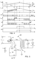
- FIG. 4 illustrates signal waveforms of signals in FIG. 3 , including, from top to bottom, line voltage V LINE , fraction result V BNO clock signal CLK, comparison result S CHK , offset current I OS , acknowledgement signal S BI , and enabling signal EN that enables or disenables signal generator 212 .
- offset current I OS is 0 A
- line voltage V LINE is under lower limit voltage V BTM , and outside a predetermined range RG defined between lower limit voltage V BTM and upper limit voltage V TOP .
- fraction result V BNO being about K*V LINE where K is the fraction defined by voltage divider 40 c , is less than reference voltage V REF .
- Acknowledgement signal S BI and comparison result S CHK both are “0” in logic. So pulse signal S RES is “0” in logic and control circuit 224 turns controllable current source 206 OFF.
- Offset current I OS is about 0 A, disappearing.
- offset current I OS makes the drop of fraction result V BNO disappear, fraction result V BNO recovers, so comparison result S CHK turns from “0” into “1” in logic.
- offset current I OS will reappear when another subsequent rising edge of clock signal CLK reaches D flip-flop 240 , and once again offset current I OS will last for only a very short period of time before it ends. In other words, offset current I OS appears periodically and lasts only for a very short period of time each time when clock signal CLK has a rising edge.
- line voltage V LINE is equal to upper limit voltage V TOP .
- line voltage V LINE is between upper limit voltage V TOP and lower limit voltage V BTM , offset current I OS appears each time when clock signal CLK has a rising edge, but offset current I OS disappears automatically soon after it appears.
- Pulse signal S RES is going to have a pulse with a pulse width of debounce-time T DEB1 defined by debouncing circuit 230 , which is 300 us for example.
- the pulse of pulse signal S RES the appearing or shutdown of offset current I OS is solely controlled by clock signal CLK, meaning that offset current I OS appears if clock signal CLK is “1” and that it disappears if clock signal CLK is “0”. This circuit behavior is illustrated by the signal waveforms in FIG. 4 during the period of time from moment t 2 to moment t 3 .
- debouncing circuit 230 turns acknowledgement signal S BI from “0” into “1” in logic, the pulse of pulse signal S RES concludes, so offset current I OS disappears or shuts down constantly, as shown at moment t 3 in FIG. 4 .
- offset current I OS appears or disappears in response to the change in logic value of clock signal CLK. More particularly, offset current I OS appears if clock signal CLK is “1”. To reduce the power consumption caused by the appearance of offset current I OS , the duty cycle of clock signal CLK, the ratio of the time when clock signal CLK is logic “1” to the cycle time of clock signal CLK, could be 10% or less.
- comparison result S CHK is stable to be “0” after moment t 4 when line voltage V LINE ramps down below lower limit voltage V BTM . So debounce-time T DEB2 after t 4 , enabling signal EN turns from “1” into “0” to disenable signal generator 212 .
- both comparator 220 comparing fraction result V BNO with reference voltage V REF and controllable current source 206 providing offset current I OS work together to check whether line voltage V LINE falls within predetermined range RG. Furthermore, if line voltage V LINE is outside predetermined range RG, offset current I OS disappears or shuts down eventually; and if line voltage V LINE is within predetermined range RG, it appears periodically and each of its appearance only lasts for a very short time period. It implies good power saving because offset current I OS is turned OFF most of time.
- Equation (1) clearly indicates that upper limit voltage V T0 p is in association with resistance RHV of current-limiting resistor 20 . Even though value IOS and reference voltage V REF are both predetermined values that cannot be changed once power controller 18 c is fabricated in form of an integrated circuit, a system designer nevertheless can choose current-limiting resistor 20 with appropriate resistance RHV to modify upper limit voltage V TOP . Bottom limit voltage V BTM is substantially independent to current-limiting resistor 20 however. Bottom limit voltage V BTM is unchangeable since it depends primarily on reference voltage V REF and K, two default factors in an integrated circuit.
- upper limit voltage V T0P is used to be the brown-in reference for brown-in mechanism, and it is adjustable by choosing current-limiting resistor 20 .
- line voltage V LINE has been steady above upper limit voltage V TOP acknowledgement signal S BI becomes “1” in logic and brown-in mechanism circuit 210 enables signal generator 212 , which according generates PWM signal S PWM to start power conversion of a power supply.
- Bottom limit voltage V BTM is used to be the brown-out reference for brown-out protection, and it cannot be adjusted when the integrated circuit of power controller 18 c completes its fabrication.
- line voltage V LINE has been steady under bottom limit voltage V BTM for more than 180 ms, output of debouncing circuit 209 becomes “1” in logic, so SR flip-flop 213 is reset to disenable signal generator 212 , thereby stopping power conversion of a power supply.
- FIG. 3 uses upper limit voltage V TOP and bottom limit voltage V BTM as brown-in and brown-out references respectively, but this invention is not limited to.
- Other embodiments of the invention could for example use upper limit voltage V TOP to be both brown-in and brown-out references.
- some embodiments of the invention could leave out brown-in mechanism circuit 210 and brown-out protection circuit 208 in FIG. 3 , and take acknowledgement signal S BI as enabling signal EN to enable or disable signal generator 212 .
- FIG. 5 demonstrates another AC-to-DC power supply 600 with a flyback topology.
- AC-to-DC power supply 600 has high-voltage startup and employs power controller 18 c of FIG. 3 .
- FIG. 5 lacks the diodes 14 in FIG. 4 , and the line voltage V LINE in FIG. 5 is provided from bridge rectifier 12 .
- Embodiments of the invention could include boosters, buck converters, buck boosters, and so forth.
Landscapes
- Engineering & Computer Science (AREA)
- Theoretical Computer Science (AREA)
- Power Engineering (AREA)
- Physics & Mathematics (AREA)
- General Engineering & Computer Science (AREA)
- General Physics & Mathematics (AREA)
- Dc-Dc Converters (AREA)
Abstract
Description
K*(V TOP −RHV*IOS)=V REF (1)
K*V BTM =V REF (2)
Claims (20)
Applications Claiming Priority (3)
| Application Number | Priority Date | Filing Date | Title |
|---|---|---|---|
| TW105130947A | 2016-09-26 | ||
| TW105130947A TWI618342B (en) | 2016-09-26 | 2016-09-26 | Line-voltage detection circuit and relevant detection method |
| TW105130947 | 2016-09-26 |
Publications (2)
| Publication Number | Publication Date |
|---|---|
| US20180088651A1 US20180088651A1 (en) | 2018-03-29 |
| US10691189B2 true US10691189B2 (en) | 2020-06-23 |
Family
ID=61685309
Family Applications (1)
| Application Number | Title | Priority Date | Filing Date |
|---|---|---|---|
| US15/692,636 Active 2038-09-22 US10691189B2 (en) | 2016-09-26 | 2017-08-31 | Line-voltage detection method, power controller and power supply with brown-out protection and brown-in mechanism |
Country Status (2)
| Country | Link |
|---|---|
| US (1) | US10691189B2 (en) |
| TW (1) | TWI618342B (en) |
Cited By (3)
| Publication number | Priority date | Publication date | Assignee | Title |
|---|---|---|---|---|
| US11211955B2 (en) | 2019-03-29 | 2021-12-28 | Samsung Electronics Co., Ltd | Voltage protection circuit to prevent power amplifier burnout, and electronic device having the same |
| US11689097B2 (en) | 2021-05-05 | 2023-06-27 | Analog Devices, Inc. | High-voltage to low-voltage interface in power converter circuit |
| US20240128736A1 (en) * | 2022-10-18 | 2024-04-18 | Hs Elektronik Systeme Gmbh | Aircraft solid state power controller and method of operating an aircraft solid state power controller |
Families Citing this family (8)
| Publication number | Priority date | Publication date | Assignee | Title |
|---|---|---|---|---|
| TWI656722B (en) * | 2017-04-28 | 2019-04-11 | 偉詮電子股份有限公司 | High voltage charging control method, power controller, and power supply |
| TWI672894B (en) * | 2018-07-25 | 2019-09-21 | 通嘉科技股份有限公司 | Power controllers and control methods thereof |
| CN110445100B (en) * | 2019-07-22 | 2024-07-19 | 江苏云意电气股份有限公司 | IGBT desaturation protection and drive power supply undervoltage protection circuit |
| IT201900017312A1 (en) * | 2019-09-27 | 2021-03-27 | St Microelectronics Srl | BROWN-OUT PROTECTION CIRCUIT FOR A SWITCHING CONVERTER AND METHOD TO CONTROL A SWITCHING CONVERTER |
| US12009743B2 (en) * | 2021-03-25 | 2024-06-11 | Stmicroelectronics S.R.L. | Method of operating an electronic converter, corresponding control circuit and electronic converter |
| US12352823B2 (en) | 2021-09-23 | 2025-07-08 | Infsitronix Technology Corporation | Method and circuit for monitoring power supply |
| CN115923517B (en) * | 2022-12-26 | 2024-08-23 | 章鱼博士智能技术(上海)有限公司 | Vehicle power reduction strategy adjustment method and device and electronic equipment |
| TWI856478B (en) * | 2023-01-09 | 2024-09-21 | 固緯電子實業股份有限公司 | Mains voltage and frequency detection circuit |
Citations (2)
| Publication number | Priority date | Publication date | Assignee | Title |
|---|---|---|---|---|
| US7486493B2 (en) * | 2005-04-07 | 2009-02-03 | System General Corporation | Over-power protection circuit for power converter |
| US20090161287A1 (en) * | 2007-12-19 | 2009-06-25 | Freescale Semiconductor, Inc. | Electronic device operable to protect a power transistor when used in conjunction with a transformer |
Family Cites Families (4)
| Publication number | Priority date | Publication date | Assignee | Title |
|---|---|---|---|---|
| US8698474B2 (en) * | 2010-06-11 | 2014-04-15 | System General Corp. | Start-up circuit with low standby power loss for power converters |
| TW201202912A (en) * | 2010-07-09 | 2012-01-16 | Leadtrend Tech Corp | Hi-V startup method and power management apparatus |
| US8670219B2 (en) * | 2011-06-16 | 2014-03-11 | Monolithic Power Systems, Inc. | High-voltage devices with integrated over-voltage protection and associated methods |
| TWI618448B (en) * | 2014-06-05 | 2018-03-11 | Leadtrend Technology Corporation | Control methods and power converters suitable for triac dimming |
-
2016
- 2016-09-26 TW TW105130947A patent/TWI618342B/en active
-
2017
- 2017-08-31 US US15/692,636 patent/US10691189B2/en active Active
Patent Citations (2)
| Publication number | Priority date | Publication date | Assignee | Title |
|---|---|---|---|---|
| US7486493B2 (en) * | 2005-04-07 | 2009-02-03 | System General Corporation | Over-power protection circuit for power converter |
| US20090161287A1 (en) * | 2007-12-19 | 2009-06-25 | Freescale Semiconductor, Inc. | Electronic device operable to protect a power transistor when used in conjunction with a transformer |
Cited By (4)
| Publication number | Priority date | Publication date | Assignee | Title |
|---|---|---|---|---|
| US11211955B2 (en) | 2019-03-29 | 2021-12-28 | Samsung Electronics Co., Ltd | Voltage protection circuit to prevent power amplifier burnout, and electronic device having the same |
| US11843398B2 (en) | 2019-03-29 | 2023-12-12 | Samsung Electronics Co., Ltd | Voltage protection circuit to prevent power amplifier burnout, and electronic device having the same |
| US11689097B2 (en) | 2021-05-05 | 2023-06-27 | Analog Devices, Inc. | High-voltage to low-voltage interface in power converter circuit |
| US20240128736A1 (en) * | 2022-10-18 | 2024-04-18 | Hs Elektronik Systeme Gmbh | Aircraft solid state power controller and method of operating an aircraft solid state power controller |
Also Published As
| Publication number | Publication date |
|---|---|
| US20180088651A1 (en) | 2018-03-29 |
| TW201815048A (en) | 2018-04-16 |
| TWI618342B (en) | 2018-03-11 |
Similar Documents
| Publication | Publication Date | Title |
|---|---|---|
| US10691189B2 (en) | Line-voltage detection method, power controller and power supply with brown-out protection and brown-in mechanism | |
| US11750083B2 (en) | Overvoltage protection circuit, integrated circuit and switching converter with the same | |
| US5814979A (en) | Low drop out switching regulator | |
| US9608509B2 (en) | Switching converter with controllable restart delay and associated control method | |
| US6469914B1 (en) | Universal pulse width modulating power converter | |
| US7230408B1 (en) | Pulse frequency modulated voltage regulator with linear regulator control | |
| KR102049372B1 (en) | Switch control circuit, switch control method, and power supply device using the same | |
| KR101365100B1 (en) | Low power consumption start-up circuit with dynamic switching | |
| US9893546B2 (en) | Direct current power supply circuit | |
| US10444780B1 (en) | Regulation/bypass automation for LDO with multiple supply voltages | |
| JP4896754B2 (en) | Overcurrent protection circuit and power supply device using the same | |
| US8063622B2 (en) | Method and apparatus for implementing slew rate control using bypass capacitor | |
| US20190140547A1 (en) | Power converter, switch control circuit and short circuit detection method for current sensing resistor of the power converter | |
| US20140125303A1 (en) | Limiting a current | |
| CN108933529B (en) | Power control device and power control system | |
| KR20110095771A (en) | Switch control device, power supply and switch control method comprising the same | |
| US20120256609A1 (en) | Error amplifier with built-in over voltage protection for switched-mode power supply controller | |
| WO2019187544A1 (en) | Power factor improvement circuit and semiconductor device | |
| US11507121B2 (en) | Recovery mechanism during an input or output voltage fault condition for a voltage regulator | |
| US20140225584A1 (en) | Switching power supply circuit | |
| US9912237B2 (en) | Switching regulator | |
| US8797772B2 (en) | Low noise voltage regulator | |
| US7176657B2 (en) | Capacitor charging circuit with a soft-start function | |
| KR101262954B1 (en) | Switching Mode Power Supply | |
| JP2014042394A (en) | Device for driving switching element |
Legal Events
| Date | Code | Title | Description |
|---|---|---|---|
| AS | Assignment |
Owner name: LEADTREND TECHNOLOGY CORPORATION, TAIWAN Free format text: ASSIGNMENT OF ASSIGNORS INTEREST;ASSIGNORS:SU, WEI CHUAN;TSAI, MENG JEN;REEL/FRAME:043464/0931 Effective date: 20170828 |
|
| FEPP | Fee payment procedure |
Free format text: ENTITY STATUS SET TO UNDISCOUNTED (ORIGINAL EVENT CODE: BIG.); ENTITY STATUS OF PATENT OWNER: SMALL ENTITY |
|
| FEPP | Fee payment procedure |
Free format text: ENTITY STATUS SET TO SMALL (ORIGINAL EVENT CODE: SMAL); ENTITY STATUS OF PATENT OWNER: SMALL ENTITY |
|
| STPP | Information on status: patent application and granting procedure in general |
Free format text: DOCKETED NEW CASE - READY FOR EXAMINATION |
|
| STPP | Information on status: patent application and granting procedure in general |
Free format text: NON FINAL ACTION MAILED |
|
| STPP | Information on status: patent application and granting procedure in general |
Free format text: NOTICE OF ALLOWANCE MAILED -- APPLICATION RECEIVED IN OFFICE OF PUBLICATIONS |
|
| STPP | Information on status: patent application and granting procedure in general |
Free format text: PUBLICATIONS -- ISSUE FEE PAYMENT VERIFIED |
|
| STCF | Information on status: patent grant |
Free format text: PATENTED CASE |
|
| MAFP | Maintenance fee payment |
Free format text: PAYMENT OF MAINTENANCE FEE, 4TH YR, SMALL ENTITY (ORIGINAL EVENT CODE: M2551); ENTITY STATUS OF PATENT OWNER: SMALL ENTITY Year of fee payment: 4 |