US10690979B2 - Display panel and method of manufacturing the same - Google Patents
Display panel and method of manufacturing the same Download PDFInfo
- Publication number
- US10690979B2 US10690979B2 US15/278,915 US201615278915A US10690979B2 US 10690979 B2 US10690979 B2 US 10690979B2 US 201615278915 A US201615278915 A US 201615278915A US 10690979 B2 US10690979 B2 US 10690979B2
- Authority
- US
- United States
- Prior art keywords
- electrode
- display panel
- thin film
- film transistor
- disposed
- Prior art date
- Legal status (The legal status is an assumption and is not a legal conclusion. Google has not performed a legal analysis and makes no representation as to the accuracy of the status listed.)
- Expired - Fee Related, expires
Links
Images


Classifications
-
- G—PHYSICS
- G02—OPTICS
- G02F—OPTICAL DEVICES OR ARRANGEMENTS FOR THE CONTROL OF LIGHT BY MODIFICATION OF THE OPTICAL PROPERTIES OF THE MEDIA OF THE ELEMENTS INVOLVED THEREIN; NON-LINEAR OPTICS; FREQUENCY-CHANGING OF LIGHT; OPTICAL LOGIC ELEMENTS; OPTICAL ANALOGUE/DIGITAL CONVERTERS
- G02F1/00—Devices or arrangements for the control of the intensity, colour, phase, polarisation or direction of light arriving from an independent light source, e.g. switching, gating or modulating; Non-linear optics
- G02F1/01—Devices or arrangements for the control of the intensity, colour, phase, polarisation or direction of light arriving from an independent light source, e.g. switching, gating or modulating; Non-linear optics for the control of the intensity, phase, polarisation or colour
- G02F1/13—Devices or arrangements for the control of the intensity, colour, phase, polarisation or direction of light arriving from an independent light source, e.g. switching, gating or modulating; Non-linear optics for the control of the intensity, phase, polarisation or colour based on liquid crystals, e.g. single liquid crystal display cells
- G02F1/133—Constructional arrangements; Operation of liquid crystal cells; Circuit arrangements
- G02F1/136—Liquid crystal cells structurally associated with a semi-conducting layer or substrate, e.g. cells forming part of an integrated circuit
- G02F1/1362—Active matrix addressed cells
- G02F1/136286—Wiring, e.g. gate line, drain line
-
- G—PHYSICS
- G02—OPTICS
- G02F—OPTICAL DEVICES OR ARRANGEMENTS FOR THE CONTROL OF LIGHT BY MODIFICATION OF THE OPTICAL PROPERTIES OF THE MEDIA OF THE ELEMENTS INVOLVED THEREIN; NON-LINEAR OPTICS; FREQUENCY-CHANGING OF LIGHT; OPTICAL LOGIC ELEMENTS; OPTICAL ANALOGUE/DIGITAL CONVERTERS
- G02F1/00—Devices or arrangements for the control of the intensity, colour, phase, polarisation or direction of light arriving from an independent light source, e.g. switching, gating or modulating; Non-linear optics
- G02F1/01—Devices or arrangements for the control of the intensity, colour, phase, polarisation or direction of light arriving from an independent light source, e.g. switching, gating or modulating; Non-linear optics for the control of the intensity, phase, polarisation or colour
- G02F1/13—Devices or arrangements for the control of the intensity, colour, phase, polarisation or direction of light arriving from an independent light source, e.g. switching, gating or modulating; Non-linear optics for the control of the intensity, phase, polarisation or colour based on liquid crystals, e.g. single liquid crystal display cells
- G02F1/137—Devices or arrangements for the control of the intensity, colour, phase, polarisation or direction of light arriving from an independent light source, e.g. switching, gating or modulating; Non-linear optics for the control of the intensity, phase, polarisation or colour based on liquid crystals, e.g. single liquid crystal display cells characterised by the electro-optical or magneto-optical effect, e.g. field-induced phase transition, orientation effect, guest-host interaction or dynamic scattering
- G02F1/139—Devices or arrangements for the control of the intensity, colour, phase, polarisation or direction of light arriving from an independent light source, e.g. switching, gating or modulating; Non-linear optics for the control of the intensity, phase, polarisation or colour based on liquid crystals, e.g. single liquid crystal display cells characterised by the electro-optical or magneto-optical effect, e.g. field-induced phase transition, orientation effect, guest-host interaction or dynamic scattering based on orientation effects in which the liquid crystal remains transparent
-
- G—PHYSICS
- G02—OPTICS
- G02F—OPTICAL DEVICES OR ARRANGEMENTS FOR THE CONTROL OF LIGHT BY MODIFICATION OF THE OPTICAL PROPERTIES OF THE MEDIA OF THE ELEMENTS INVOLVED THEREIN; NON-LINEAR OPTICS; FREQUENCY-CHANGING OF LIGHT; OPTICAL LOGIC ELEMENTS; OPTICAL ANALOGUE/DIGITAL CONVERTERS
- G02F1/00—Devices or arrangements for the control of the intensity, colour, phase, polarisation or direction of light arriving from an independent light source, e.g. switching, gating or modulating; Non-linear optics
- G02F1/01—Devices or arrangements for the control of the intensity, colour, phase, polarisation or direction of light arriving from an independent light source, e.g. switching, gating or modulating; Non-linear optics for the control of the intensity, phase, polarisation or colour
- G02F1/13—Devices or arrangements for the control of the intensity, colour, phase, polarisation or direction of light arriving from an independent light source, e.g. switching, gating or modulating; Non-linear optics for the control of the intensity, phase, polarisation or colour based on liquid crystals, e.g. single liquid crystal display cells
- G02F1/133—Constructional arrangements; Operation of liquid crystal cells; Circuit arrangements
- G02F1/1333—Constructional arrangements; Manufacturing methods
- G02F1/1335—Structural association of cells with optical devices, e.g. polarisers or reflectors
- G02F1/133509—Filters, e.g. light shielding masks
- G02F1/133514—Colour filters
-
- G—PHYSICS
- G02—OPTICS
- G02F—OPTICAL DEVICES OR ARRANGEMENTS FOR THE CONTROL OF LIGHT BY MODIFICATION OF THE OPTICAL PROPERTIES OF THE MEDIA OF THE ELEMENTS INVOLVED THEREIN; NON-LINEAR OPTICS; FREQUENCY-CHANGING OF LIGHT; OPTICAL LOGIC ELEMENTS; OPTICAL ANALOGUE/DIGITAL CONVERTERS
- G02F1/00—Devices or arrangements for the control of the intensity, colour, phase, polarisation or direction of light arriving from an independent light source, e.g. switching, gating or modulating; Non-linear optics
- G02F1/01—Devices or arrangements for the control of the intensity, colour, phase, polarisation or direction of light arriving from an independent light source, e.g. switching, gating or modulating; Non-linear optics for the control of the intensity, phase, polarisation or colour
- G02F1/13—Devices or arrangements for the control of the intensity, colour, phase, polarisation or direction of light arriving from an independent light source, e.g. switching, gating or modulating; Non-linear optics for the control of the intensity, phase, polarisation or colour based on liquid crystals, e.g. single liquid crystal display cells
- G02F1/133—Constructional arrangements; Operation of liquid crystal cells; Circuit arrangements
- G02F1/1333—Constructional arrangements; Manufacturing methods
- G02F1/1343—Electrodes
- G02F1/134309—Electrodes characterised by their geometrical arrangement
-
- G—PHYSICS
- G02—OPTICS
- G02F—OPTICAL DEVICES OR ARRANGEMENTS FOR THE CONTROL OF LIGHT BY MODIFICATION OF THE OPTICAL PROPERTIES OF THE MEDIA OF THE ELEMENTS INVOLVED THEREIN; NON-LINEAR OPTICS; FREQUENCY-CHANGING OF LIGHT; OPTICAL LOGIC ELEMENTS; OPTICAL ANALOGUE/DIGITAL CONVERTERS
- G02F1/00—Devices or arrangements for the control of the intensity, colour, phase, polarisation or direction of light arriving from an independent light source, e.g. switching, gating or modulating; Non-linear optics
- G02F1/01—Devices or arrangements for the control of the intensity, colour, phase, polarisation or direction of light arriving from an independent light source, e.g. switching, gating or modulating; Non-linear optics for the control of the intensity, phase, polarisation or colour
- G02F1/13—Devices or arrangements for the control of the intensity, colour, phase, polarisation or direction of light arriving from an independent light source, e.g. switching, gating or modulating; Non-linear optics for the control of the intensity, phase, polarisation or colour based on liquid crystals, e.g. single liquid crystal display cells
- G02F1/133—Constructional arrangements; Operation of liquid crystal cells; Circuit arrangements
- G02F1/136—Liquid crystal cells structurally associated with a semi-conducting layer or substrate, e.g. cells forming part of an integrated circuit
- G02F1/1362—Active matrix addressed cells
- G02F1/136209—Light shielding layers, e.g. black matrix, incorporated in the active matrix substrate, e.g. structurally associated with the switching element
-
- G—PHYSICS
- G02—OPTICS
- G02F—OPTICAL DEVICES OR ARRANGEMENTS FOR THE CONTROL OF LIGHT BY MODIFICATION OF THE OPTICAL PROPERTIES OF THE MEDIA OF THE ELEMENTS INVOLVED THEREIN; NON-LINEAR OPTICS; FREQUENCY-CHANGING OF LIGHT; OPTICAL LOGIC ELEMENTS; OPTICAL ANALOGUE/DIGITAL CONVERTERS
- G02F1/00—Devices or arrangements for the control of the intensity, colour, phase, polarisation or direction of light arriving from an independent light source, e.g. switching, gating or modulating; Non-linear optics
- G02F1/01—Devices or arrangements for the control of the intensity, colour, phase, polarisation or direction of light arriving from an independent light source, e.g. switching, gating or modulating; Non-linear optics for the control of the intensity, phase, polarisation or colour
- G02F1/13—Devices or arrangements for the control of the intensity, colour, phase, polarisation or direction of light arriving from an independent light source, e.g. switching, gating or modulating; Non-linear optics for the control of the intensity, phase, polarisation or colour based on liquid crystals, e.g. single liquid crystal display cells
- G02F1/133—Constructional arrangements; Operation of liquid crystal cells; Circuit arrangements
- G02F1/136—Liquid crystal cells structurally associated with a semi-conducting layer or substrate, e.g. cells forming part of an integrated circuit
- G02F1/1362—Active matrix addressed cells
- G02F1/1368—Active matrix addressed cells in which the switching element is a three-electrode device
-
- G—PHYSICS
- G02—OPTICS
- G02F—OPTICAL DEVICES OR ARRANGEMENTS FOR THE CONTROL OF LIGHT BY MODIFICATION OF THE OPTICAL PROPERTIES OF THE MEDIA OF THE ELEMENTS INVOLVED THEREIN; NON-LINEAR OPTICS; FREQUENCY-CHANGING OF LIGHT; OPTICAL LOGIC ELEMENTS; OPTICAL ANALOGUE/DIGITAL CONVERTERS
- G02F1/00—Devices or arrangements for the control of the intensity, colour, phase, polarisation or direction of light arriving from an independent light source, e.g. switching, gating or modulating; Non-linear optics
- G02F1/01—Devices or arrangements for the control of the intensity, colour, phase, polarisation or direction of light arriving from an independent light source, e.g. switching, gating or modulating; Non-linear optics for the control of the intensity, phase, polarisation or colour
- G02F1/13—Devices or arrangements for the control of the intensity, colour, phase, polarisation or direction of light arriving from an independent light source, e.g. switching, gating or modulating; Non-linear optics for the control of the intensity, phase, polarisation or colour based on liquid crystals, e.g. single liquid crystal display cells
- G02F1/137—Devices or arrangements for the control of the intensity, colour, phase, polarisation or direction of light arriving from an independent light source, e.g. switching, gating or modulating; Non-linear optics for the control of the intensity, phase, polarisation or colour based on liquid crystals, e.g. single liquid crystal display cells characterised by the electro-optical or magneto-optical effect, e.g. field-induced phase transition, orientation effect, guest-host interaction or dynamic scattering
- G02F1/13756—Devices or arrangements for the control of the intensity, colour, phase, polarisation or direction of light arriving from an independent light source, e.g. switching, gating or modulating; Non-linear optics for the control of the intensity, phase, polarisation or colour based on liquid crystals, e.g. single liquid crystal display cells characterised by the electro-optical or magneto-optical effect, e.g. field-induced phase transition, orientation effect, guest-host interaction or dynamic scattering the liquid crystal selectively assuming a light-scattering state
-
- G02F2001/13756—
-
- G—PHYSICS
- G02—OPTICS
- G02F—OPTICAL DEVICES OR ARRANGEMENTS FOR THE CONTROL OF LIGHT BY MODIFICATION OF THE OPTICAL PROPERTIES OF THE MEDIA OF THE ELEMENTS INVOLVED THEREIN; NON-LINEAR OPTICS; FREQUENCY-CHANGING OF LIGHT; OPTICAL LOGIC ELEMENTS; OPTICAL ANALOGUE/DIGITAL CONVERTERS
- G02F2203/00—Function characteristic
- G02F2203/64—Normally black display, i.e. the off state being black
Definitions
- Exemplary embodiments of the inventive concept relate to a display panel and a method of manufacturing the display panel. More particularly, exemplary embodiments of the inventive concept relate to a transparent display panel and a method of manufacturing the transparent display panel.
- a cathode ray tube (CRT) display apparatus has been used due to a performance and a competitive price.
- the CRT display apparatus has a weakness with a size or portability. Therefore, a display apparatus such as a plasma display apparatus, a liquid crystal display apparatus and an organic light emitting display apparatus has been highly regarded due to small size, light weight and low-power-consumption.
- the liquid crystal display may have various pixel structures according to driving method. Various efforts have been made to improve aperture ratio and transmittance.
- One or more exemplary embodiment of the inventive concept provides a display panel capable of improving transmittance and control the transmittance.
- One or more exemplary embodiments of the inventive concept also provide a method of manufacturing the display panel.
- a display panel includes a first base substrate, a gate line and a data line, a thin film transistor disposed on the first base substrate, and electrically connected to the gate line and the data line, a first electrode electrically connected to the thin film transistor, a third electrode spaced apart from the first electrode in a plan view, a second electrode facing the first electrode and the third electrode, and entirely overlapping the data line in a first direction, and a liquid crystal layer disposed between the first and third electrodes and the second electrode.
- a portion of the liquid crystal layer between the third electrode and the second electrode when on voltage is configured to be applied to the third electrode, a portion of the liquid crystal layer between the third electrode and the second electrode may be configured to pass light.
- off voltage when off voltage is configured to be applied to the third electrode, the portion of the liquid crystal layer between the third electrode and the second electrode may be configured to block light.
- a common voltage may be configured to be applied to the second electrode, and a difference between the off voltage and the common voltage may be less than 1.5V (voltage).
- a voltage having a value between the on voltage and the off voltage may be configured to be applied to the third electrode.
- a portion of the third electrode may overlap the data line.
- the third electrode may be configured not to be electrically connected to the thin film transistor in a pixel.
- the display panel may further include a color filter which is disposed to overlap the first electrode, and not to overlap the third electrode.
- the first electrode and the third electrode may include a same material.
- the first electrode and the third electrode may be disposed in a same plane.
- the display panel may further include a light blocking pattern overlapping the thin film transistor.
- the light blocking pattern may be not connected to and spaced apart from a light blocking pattern of an adjacent pixel.
- the first electrode may include a first high electrode and a first low electrode.
- the thin film transistor may include a first thin film transistor and a second thin film transistor.
- the first high electrode may be electrically connected to the first thin film transistor.
- the first low electrode may be electrically connected to the second thin film transistor.
- the display panel may further include a third thin film transistor and a dividing reference voltage line extending in parallel with the data line.
- the third thin film transistor may be electrically connected to the dividing reference voltage line and the second thin film transistor.
- a dividing reference voltage may be configured to be applied to the dividing reference voltage line.
- the dividing reference voltage line may not overlap the first high electrode and the first low electrode.
- the third electrode may include a first stem extending in a first direction, a second stem extending in a second direction which crosses the first direction, and a plurality of slit portions extending in a direction which is inclined with respect to the first and second directions.
- the slit portions may form a plurality of slits.
- the third electrode may include a connecting electrode extending in parallel with the gate line.
- the connecting electrode may be electrically connected to a third electrode of an adjacent pixel.
- the third electrode may overlap the thin film transistor.
- a method of manufacturing a display panel includes forming a thin film transistor on a first base substrate, forming a first electrode and a third electrode by patterning a pixel electrode layer after forming the pixel electrode layer on the thin film transistor, forming a second electrode which faces the first and third electrodes on a second base substrate, forming a color filter which overlaps the first electrode on the second base substrate, and forming a liquid crystal layer between the first substrate and the second substrate.
- the pixel electrode layer includes transparent conductive material.
- the third electrode is electrically connected to the thin film transistor.
- the third electrode is spaced apart from the first electrode.
- the color filter does not overlap the third electrode.
- a display panel includes a first electrode electrically connected to a data line and a gate line, a third electrode, wherein voltages different from each other are configured to be applied thereto according to a transparent mode or a normal mode, a second electrode facing the first and third electrodes, wherein a common voltage is configured to be applied thereto, and a liquid crystal layer disposed between the first and third electrodes and the second electrode.
- the display panel is configured to work as a transparent display device which is transparent to display an image in the transparent mode.
- the display panel is configured to work as a normal display device which is not transparent to display an image in the normal mode.
- a display panel includes a first electrode, a second electrode, a third electrode and a liquid crystal layer to embody a transparent mode and a normal mode.
- a transparent mode an on voltage is applied to the third electrode, and a common voltage is applied to the second electrode. Accordingly, the liquid crystal layer passes light, so that the display panel can work as a transparent display.
- the normal mode an off voltage is applied to the third electrode, and the common voltage is applied to the second electrode. Accordingly, the liquid crystal layer blocks light, so that the display panel can work as a traditional display.
- the display panel may minimize size of a light blocking pattern, and may improve transparency of the display panel by designing a shape of the third electrode.
- the transparency may be controlled by adjusting voltage level applied to the third electrode.
- FIG. 1 is a plan view illustrating one pixel of a display panel according to an exemplary embodiment of the inventive concept
- FIG. 2 is a cross-sectional view taken along a line I-I′ of FIG. 1 ;
- FIG. 3 is a plan view illustrating a first high electrode, a first low electrode and third electrode of the display panel of FIG. 1 in detail;
- FIG. 4 is an equivalent circuit diagram of the pixel of FIG. 1 ;
- FIG. 5 is a plan view illustrating one pixel of a display panel according to an exemplary embodiment of the inventive concept
- FIG. 6 is a plan view illustrating one pixel of a display panel according to an exemplary embodiment of the inventive concept
- FIG. 7 is a plan view illustrating one pixel of a display panel according to an exemplary embodiment of the inventive concept
- FIG. 8 is a plan view illustrating one pixel of a display panel according to an exemplary embodiment of the inventive concept
- FIG. 9 is a plan view illustrating one pixel of a display panel according to an exemplary embodiment of the inventive concept.
- FIG. 10 is a plan view illustrating one pixel of a display panel according to an exemplary embodiment of the inventive concept.
- FIGS. 11A, 11B, 12A, 12B, 13A, 13B, 14, 15A and 15B are plan views and cross-sectional views illustrating a method of manufacturing the display panel of FIG. 1 .
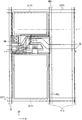
- FIG. 1 is a plan view illustrating one pixel of a display panel according to an exemplary embodiment of the inventive concept.
- FIG. 2 is a cross-sectional view taken along a line I-I′ of FIG. 1 .
- the display panel may include a first base substrate 100 , a gate line GL, a high storage pattern CSTh, a low storage pattern CSTl, a first insulation layer 110 , a data line DL, a voltage dividing reference voltage line RDL, a second insulation layer 120 , a first high electrode EL 1 h , a first low electrode EL 1 l , a third electrode EL 3 , a second base substrate 200 , a light blocking pattern BM, a color filter 210 , an over-coating layer 220 , a second electrode EL 2 and a liquid crystal layer 300 .
- the first base substrate 100 may include a transparent insulation substrate.
- the first base substrate 100 may include a glass substrate, a quartz substrate, a transparent resin substrate, etc.
- the transparent resin substrate for the first base substrate 100 may include polyimide-based resin, acryl-based resin, polyacrylate-based resin, polycarbonate-based resin, polyether-based resin, sulfonic acid containing resin, polyethyleneterephthalate-based resin, etc.
- the gate line GL may be disposed on the first base substrate 100 .
- the gate line GL may be extended in a first direction D 1 .
- the gate line GL may be electrically connected to a first gate electrode GE 1 .
- the first gate electrode GE 1 may be a portion of the gate line GL.
- the gate line GL may be electrically connected to a second gate electrode and a third gate electrode.
- the second gate electrode and the third gate electrode may be a portion of the gate line GL.
- the gate line GL may include metal, alloy, conductive metal oxide, a transparent conductive material, etc.
- a buffer layer may be disposed between the first base substrate 100 and the gate line GL.
- the buffer layer may prevent diffusion of metal atoms and/or impurities from the first base substrate 100 .
- the buffer layer may improve flatness of the surface of the first base substrate 100 .
- the buffer layer may be formed using a silicon compound.
- the buffer layer may include silicon oxide (SiOx), silicon nitride (SiNx), silicon oxynitride (SiOxNy), silicon oxycarbide (SiOxCy), silicon carbon nitride (SiCxNy), etc. These may be used alone or in a mixture thereof.
- the buffer layer may have a single layer structure or a multi layer structure.
- the buffer layer may have a single-layered structure including a silicon oxide film, a silicon nitride film, a silicon oxynitride film, a silicon oxycarbide film or a silicon carbon nitride film.
- the buffer layer may have a multilayered structure including at least two of a silicon oxide film, a silicon nitride film, a silicon oxynitride film, a silicon oxycarbide film, a silicon carbon nitride film, etc.
- the high storage pattern CSTh may be disposed on the first base substrate 100 .
- the high storage pattern CSTh may be electrically connected to a high storage pattern of an adjacent pixel in the first direction D 1 .
- the high storage pattern CSTh may be overlapped with a boundary of the first high electrode EL 1 h .
- a storage voltage may be applied to the high storage pattern CSTh.
- the high storage pattern CSTh may include metal, alloy, conductive metal oxide, a transparent conductive material, etc.
- the low storage pattern CSTl may be disposed on the first base substrate 100 .
- the low storage pattern CSTl may be electrically connected to a low storage pattern of the adjacent pixel in the first direction D 1 .
- the low storage pattern CSTl may be overlapped with a boundary of the first low electrode EL 1 l .
- a storage voltage may be applied to the low storage pattern CSTl.
- the first insulation layer 110 may be disposed on the first base substrate 100 on which the gate line GL, the high storage pattern CSTh and the low storage pattern CSTl are disposed.
- the first insulation layer 110 may include a silicon compound, metal oxide, etc.
- the first insulation layer 110 may be formed using silicon oxide (SiOx), silicon nitride (SiNx), silicon oxynitride (SiOxNy), aluminum oxide (AlOx), tantalum oxide (TaOx), hafnium oxide (HfOx), zirconium oxide (ZrOx), titanium oxide (TiOx), etc. These may be used alone or in a combination thereof.
- the first insulation layer 110 may have a single layer structure or a multi layer structure including the silicon oxide and/or the silicon nitride.
- the first insulation layer 110 may be uniformly formed on the first base substrate 100 along a profile of the gate line GL, the high storage pattern CSTh and the low storage pattern CSTl.
- the first insulation layer 110 may have a substantially small thickness, such that a stepped portion may be formed at a portion of the gate line GL, the high storage pattern CSTh and the low storage pattern CSTl.
- the first insulation layer 110 may have a relatively large thickness for sufficiently covering the gate line GL, the high storage pattern CSTh and the low storage pattern CSTl.
- the active pattern may be disposed on the first insulation layer 110 .
- the active pattern may include a first active area ACT 1 , a second active area, and a third active area.
- the first active area ACT 1 may be overlapped with the first gate electrode GE 1 .
- the second active area may be overlapped with the second gate electrode.
- the third active area may be overlapped with the third gate electrode.
- the active pattern may include a semiconductor layer consisting of amorphous silicon (a-Si:H) and an ohmic contact layer consisting of n+ amorphous silicon (n+ a-Si:H).
- the active pattern may include an oxide semiconductor.
- the oxide semiconductor may include an amorphous oxide including at least one selected from the group consisting of indium (In), zinc (Zn), gallium (Ga), tin (Sn) and hafnium (Hf).
- the data line DL may be disposed on the first insulation layer 110 .
- the data line DL may be extended in a second direction D 2 which crosses the first direction D 1 .
- the second direction D 2 may be substantially perpendicular to the first direction D 1 .
- the data line DL may be electrically connected to a first source electrode SE 1 and a second source electrode.
- the data line DL may include metal, alloy, conductive metal oxide, a transparent conductive material, etc.
- the first source electrode SE 1 may be electrically connected to the first active area ACT 1 of the active pattern.
- a first drain electrode DE 1 may be spaced apart from the first source electrode SE 1 , and electrically connected to the first active area ACT 1 of the active pattern.
- the second source electrode may be electrically connected to the second active area of the active pattern.
- a second drain electrode may be spaced apart from the second source electrode, and electrically connected to the second active area of the active pattern.
- the voltage dividing reference voltage line RDL may be disposed on the first insulation layer 110 .
- the voltage dividing reference voltage line RDL may be spaced apart from the data line DL in the first direction D 1 , and extend in the second direction D 2 .
- the voltage dividing reference voltage line RDL may be electrically connected to a third drain electrode.
- the voltage dividing reference voltage line RDL may include metal, alloy, conductive metal oxide, a transparent conductive material, etc.
- the third drain electrode may be electrically connected to the third active area of the active pattern.
- a third source electrode may be spaced apart from the third drain electrode, and electrically connected to the third active area of the active pattern.
- the third source electrode may be electrically connected to the second drain electrode.
- the first gate electrode GE 1 , the first source electrode SE 1 , the first drain electrode DE 1 , the first active area ACT 1 of the active pattern may be included in a first thin film transistor TFT 1 .
- the second gate electrode, the second source electrode, the second drain electrode, the second active area of the active pattern may be included in a second thin film transistor TFT 2 .
- the third gate electrode, the third source electrode, the third drain electrode, the third active area of the active pattern may be included in a third thin film transistor TFT 3 .
- the second insulation layer 120 may be disposed on first insulation layer 110 on which the data line DL and the voltage dividing reference voltage line RDL are disposed.
- the second insulation layer 120 may include a silicon compound, metal oxide, etc.
- the second insulation layer 120 may be formed using silicon oxide (SiOx), silicon nitride (SiNx), silicon oxynitride (SiOxNy), aluminum oxide (AlOx), tantalum oxide (TaOx), hafnium oxide (HfOx), zirconium oxide (ZrOx), titanium oxide (TiOx), etc. These may be used alone or in a combination thereof.
- the second insulation layer 120 may have a single layer structure or a multi layer structure including the silicon oxide and/or the silicon nitride.
- the second insulation layer 120 may have a relatively large thickness for sufficiently covering the data line DL and the voltage dividing reference voltage line RDL, so that the second insulation layer 120 may have a substantially flat upper surface.
- the second insulation layer 120 may be uniformly formed on the first insulation layer 110 along a profile of the data line DL and the voltage dividing reference voltage line RDL.
- the second insulation layer 120 may have a substantially small thickness.
- the first insulation layer 110 may have a relatively large thickness for sufficiently covering the gate line GL, the high storage pattern CSTh and the low storage pattern CSTl.
- the first high electrode EL 1 h may be disposed on the second insulation layer 120 .
- the first high electrode EL 1 h may be electrically connected to the first drain electrode DE 1 of the first thin film transistor TFT 1 through a contact hole form through the second insulation layer 120 .
- Boundary of the first high electrode EL 1 h may be overlapped with a portion of the high storage pattern CSTh.
- the first high electrode EL 1 h may include transparent conductive material.
- the first high electrode EL 1 h may include indium tin oxide (ITO), indium zinc oxide (IZO) and etc.
- the first low electrode EL 1 l may be disposed on the second insulation layer 120 .
- the first low electrode EL 1 l may be spaced apart from the first high electrode EL 1 h in the second direction D 2 .
- the first low electrode EL 1 l may be electrically connected to the second drain electrode of the second thin film transistor TFT 2 and the third source electrode of the third transistor though a contact hole form through the second insulation layer 120 . Boundary of the first low electrode EL 1 l may be overlapped with a portion of the low storage pattern CSTl.
- the first low electrode EL 1 l may include transparent conductive material.
- the first low electrode EL 1 l may include indium tin oxide (ITO), indium zinc oxide (IZO) and etc.
- the third electrode EL 3 may be disposed on the second insulation layer 120 , and spaced apart from the first high electrode EL 1 h and the first low electrode EL 1 l in the first direction D 1 .
- the third electrode EL 3 may extend in the second direction D 2 .
- the third electrode EL 3 may overlap the voltage dividing reference voltage line RDL and a data line of an adjacent pixel. On or off voltage may be applied to the third electrode EL 3 for converting a transparent mode to a normal mode and vise versa.
- the third electrode EL 3 may extend in the first direction D 1 , and may be electrically connected to a third electrode of the adjacent pixel through a connecting electrode which is disposed between the first high electrode EL 1 h and the first low electrode EL 1 l.
- the third electrode EL 3 may include transparent conductive material.
- the third electrode EL 3 may include indium tin oxide (ITO), indium zinc oxide (IZO) and etc.
- the second base substrate 200 may be disposed to face the first substrate 100 .
- the second base substrate 200 may include a transparent insulation substrate.
- the second base substrate 200 may include a glass substrate, a quartz substrate, a transparent resin substrate, etc.
- the transparent resin substrate for the second base substrate 200 may include polyimide-based resin, acryl-based resin, polyacrylate-based resin, polycarbonate-based resin, polyether-based resin, sulfonic acid containing resin, polyethyleneterephthalate-based resin, etc.
- the light blocking pattern BM may be disposed on the second base substrate 200 .
- the light blocking pattern BM may include a material which blocks light.
- the light blocking pattern BM may overlap the first to third thin film transistors TFT 1 , TFT 2 and TFT 3 .
- the color filter 210 may be disposed on the second substrate 200 on which the light blocking pattern BM is disposed.
- the color filter 210 supplies colors to the light passing through the liquid crystal layer 300 .
- the color filter 210 may include a red color filter, a green color filter and blue color filter.
- the color filter 210 corresponds to the pixel.
- the color filters adjacent to each other may have different colors.
- the color filter 210 may be overlapped with adjacent color filter in a boundary of the adjacent pixels. In addition, the color filter 210 may be spaced apart from adjacent color filter in the boundary of the adjacent pixels.
- the color filter 210 may be disposed not to overlap the first electrode EL 1 .
- the color filter 210 may be spaced apart from the third electrode EL 3 in a plan view.
- the over-coating layer 220 may be disposed on the color filter 210 and the light blocking pattern BM.
- the over-coating layer 220 may flatten, protect, and insulate the color filter CF.
- the over-coating layer 220 may include acrylic-epoxy material.
- the second electrode EL 2 may be disposed on the over-coating layer 220 .
- the second electrode EL 2 may face the first high electrode EL 1 h and the first low electrode EL 1 l .
- the second electrode EL 2 may face the third electrode EL 3 .
- a common voltage may be applied to the second electrode EL 2 .
- the second electrode EL 2 may include a transparent conductive material.
- the second electrode EL 2 may include indium tin oxide (ITO), indium zinc oxide (IZO) and etc.
- the liquid crystal layer 300 may be disposed between the first high and low electrodes EL 1 h and EL 1 l and the second electrode EL 2 . In addition, the liquid crystal layer 300 may be disposed between the third electrode EL 3 and the second electrode EL 2 .
- the liquid crystal layer 300 includes liquid crystal molecules having optical anisotropy. The liquid crystal molecules are driven by electric field, so that an image is displayed by passing or blocking light through the liquid crystal layer 300 .
- the on voltage is applied to the third electrode EL 3 , and the common voltage is applied to the second electrode EL 2 . Accordingly, the liquid crystal layer 300 passes light, so that the display panel can work as a transparent display.
- the off voltage is applied to the third electrode EL 3
- the common voltage is applied to the second electrode EL 2 .
- the liquid crystal layer 300 blocks light, so that the display panel can work as a traditional display.
- a portion of the liquid crystal layer 300 which corresponds to the third electrode EL 3 , blocks the light, so that the portion may work as a light blocking portion.
- difference between the off voltage and the common voltage may be less than about 1.5V.
- the off voltage may preferably be same value as the common voltage.
- the display panel displays a black image when voltage difference between upper surface and lower surface of the liquid crystal layer is zero, and the display panel displays an image which is formed by light passing the liquid crystal layer when the voltage difference between upper surface and lower surface of the liquid crystal layer is not zero.
- the portion of the liquid crystal layer 300 which corresponds to the third electrode EL 3 may pass or block light according to the transparent and normal modes.
- the display apparatus works in a normally black mode in the present example embodiment
- the display apparatus may work in a normally white mode in a similar manner as that of the present example embodiment.
- transparency may be controlled by adjusting the voltage level applied to the third electrode EL 3 .
- the voltage level may be between the on voltage and the off voltage.
- FIG. 3 is a plan view illustrating the first high electrode EL 1 h , the first low electrode EL 1 l and the third electrode EL 3 of the display panel of FIG. 1 in detail.
- each of the first high electrode EL 1 h , the first low electrode EL 1 l and the third electrode EL 3 may have slit structure.
- the first high electrode EL 1 h and the first low electrode EL 1 l are sometimes called the first high pixel electrode EL 1 h and the first low pixel electrode EL 1 l.
- the first high pixel electrode EL 1 h may include a first stem 131 , a second stem 132 and a plurality of slit portions 133 .
- the first stem 131 may extend in a first direction D 1 .
- the second stem 132 may extend in a second direction D 2 crossing the first direction D 1 .
- the slit portion 133 may be extended from the first stem 131 or the second stem 132 in a direction which is inclined with respect to the first and second directions D 1 and D 2 .
- the slit portion 133 may form a plurality of slits.
- the first low pixel electrode EL 1 l may include a first stem 134 , a second stem 135 and a plurality of slit portions 136 .
- the first stem 134 may extend in the first direction D 1 .
- the second stem 135 may extend in the second direction D 2 .
- the slit portion 136 may be extended from the first stem 134 or the second stem 135 in a direction which is inclined with respect to the first and second directions D 1 and D 2 .
- the slit portion 136 may form a plurality of slits.
- the third electrode EL 3 may include a first stem 137 , a second stem 138 and a plurality of slit portions 139 .
- the first stem 137 may extend in the first direction D 1 .
- the second stem 138 may extend in the second direction D 2 .
- the slit portion 139 may be extended from the first stem 137 or the second stem 138 in a direction which is inclined with respect to the first and second directions D 1 and D 2 .
- the slit portion 139 may form a plurality of slits.
- Control for the liquid crystal molecules of the liquid crystal layer may be improved by the slit structure, so that visibility of the display panel may be improved.
- the third electrode EL 3 has the slit structure in the present embodiment, it is not to be construed as limiting thereof.
- the third electrode EL 3 may have a planer shape without the slit structure.
- FIG. 4 is an equivalent circuit diagram of the pixel of FIG. 1 .
- the pixel of the display panel may include a plurality of signal lines, first, second, and third thin film transistors TFT 1 , TFT 2 and TFT 3 which are electrically connected to the signal lines, a high liquid crystal capacitor HClc, a low liquid crystal capacitor LClc, a high storage capacitor HCST, and a low storage capacitor LCST.
- the signal lines may include a gate line GL, a high storage pattern CSTh, a low storage pattern CSTl, a data line DL and a dividing reference voltage line RDL.
- the high storage pattern CSTh, a first high electrode EL 1 h and first and second insulation layers 110 and 120 therebetween may form the high storage capacitor HCST.
- the low storage pattern CSTl, a first low electrode EL 1 l and the second insulation layers 110 and 120 therebetween may form the low storage capacitor LCST.
- a gate signal GATE may be applied to the gate line GL.
- a data signal DATA may be applied to the data line DL.
- a dividing reference voltage VRD may be applied to the voltage dividing reference voltage line RDL.
- a common voltage Vcom may be applied to the second electrode EL 2 .
- a storage voltage Vcst may be applied to the high storage pattern CSTh.
- the storage voltage Vcst may be applied to the low storage pattern CSTl.
- a voltage applied to the high storage pattern CSTh and a voltage applied to the low storage pattern CSTl may be different from each other.
- the first thin film transistor TFT 1 , the second thin film transistor TFT 2 and the third thin film transistor TFT 3 may be turned on. Accordingly, a data voltage applied to the data line DL may be applied to the first high electrode EL 1 h though the first thin film transistor TFT 1 which is turned on.
- the high liquid crystal capacitor HClc may be charged by a difference between the common voltage Vcom and the data voltage.
- the data voltage may be divided by the second thin film transistor TFT 2 which is turned on, and the third thin film transistor TFT 3 which is turned on, and charged to the low liquid crystal capacitor LClc.
- a charged value of the low liquid crystal capacitor LClc may be lower than that of the high liquid crystal capacitor HClc.
- FIG. 5 is a plan view illustrating one pixel of a display panel according to an exemplary embodiment of the inventive concept.
- the display panel may be substantially same as the display panel of FIG. 1 , except for a shape of a third electrode EL 3 , and presence or absence of a light blocking pattern.
- a shape of a third electrode EL 3 and presence or absence of a light blocking pattern.
- the display panel may include a first base substrate, a gate line GL, a high storage pattern CSTh, a low storage pattern CSTl, a first insulation layer, a data line DL, a voltage dividing reference voltage line RDL, a second insulation layer, a first high electrode EL 1 h , a first low electrode EL 1 l , a third electrode EL 3 , a second base substrate, a color filter, an over-coating layer, a second electrode and a liquid crystal layer.
- the first base substrate may include a transparent insulation substrate.
- the gate line GL may be disposed on the first base substrate.
- the high storage pattern CSTh may be disposed on the first base substrate.
- the low storage pattern CSTl may be disposed on the first base substrate.
- the first insulation layer may be disposed on the first base substrate on which the gate line GL, the high storage pattern CSTh and the low storage pattern CSTl are disposed.
- An active pattern may be disposed on the first insulation layer.
- the data line DL may be disposed on the first insulation layer.
- the voltage dividing reference voltage line RDL may be disposed on the first insulation layer.
- the second insulation layer may be disposed on first insulation layer on which the data line DL and the voltage dividing reference voltage line RDL are disposed.
- the first high electrode EL 1 h may be disposed on the second insulation layer.
- the first low electrode EL 1 l may be disposed on the second insulation layer.
- the third electrode EL 3 may be disposed on the second insulation layer.
- the second base substrate may be disposed to face the first substrate.
- the color filter may be disposed on the second substrate.
- the over-coating layer may be disposed on the color filter.
- the second electrode may be disposed on the over-coating layer.
- the liquid crystal layer may be disposed between the first high and low electrodes EL 1 h and EL 1 l and the second electrode EL 2 .
- the gate line GL may extend in a first direction D 1 .
- the high storage pattern CSTh may be electrically connected to a high storage pattern of an adjacent pixel in the first direction D 1 .
- the low storage pattern CSTl may be electrically connected to a low storage pattern of the adjacent pixel in the first direction D 1 .
- the second data line DL may extend in a second direction D 2 which crosses the first direction D 1 .
- the second direction D 2 may be substantially perpendicular to the first direction D 1 .
- the voltage dividing reference voltage line RDL may be spaced apart from the data line DL in the first direction D 1 , and extend in the second direction D 2 .
- the first high electrode EL 1 h may be electrically connected to a first drain electrode of the first thin film transistor TFT 1 through a contact hole formed through the second insulation layer. A boundary of the first high electrode EL 1 h may be overlapped with a portion of the high storage pattern CSTh.
- the first high electrode EL 1 h may include transparent conductive material.
- the first high electrode EL 1 h may include indium tin oxide (ITO), indium zinc oxide (IZO) and etc.
- the first low electrode EL 1 l may be spaced apart from the first high electrode EL 1 h in the second direction D 2 .
- the first low electrode EL 1 l may be electrically connected to a second drain electrode of the second thin film transistor TFT 2 and a third source electrode of the third transistor TFT 3 through a contact hole formed through the second insulation layer.
- a boundary of the first low electrode EL 1 l may be overlapped with a portion of the low storage pattern CSTl.
- the first low electrode EL 1 l may include transparent conductive material.
- the first low electrode EL 1 l may include indium tin oxide (ITO), indium zinc oxide (IZO) and etc.
- the third electrode EL 3 may be spaced apart from the first high electrode EL 1 h and the first low electrode EL 1 l .
- the third electrode EL 3 may extend in the second direction D 2 .
- the third electrode EL 3 may overlap the voltage dividing reference voltage line RDL and a data line of an adjacent pixel. On or off voltage may be applied to the third electrode EL 3 for converting a transparent mode to a normal mode and vise versa.
- the third electrode EL 3 may extend in the first direction D 1 , and may be electrically connected to a third electrode of the adjacent pixel.
- the third electrode EL 3 may overlap the first to third thin film transistors TFT 1 , TFT 2 and TFT 3 .
- the third electrode EL 3 may block light in the normal mode. Accordingly, an additional light blocking pattern needs not to be formed on a color filter substrate.
- the third electrode EL 3 may include transparent conductive material.
- the third electrode EL 3 may include indium tin oxide (ITO), indium zinc oxide (IZO) and etc.
- FIG. 6 is a plan view illustrating one pixel of a display panel according to an exemplary embodiment of the inventive concept.
- the display panel may include a gate line GL, a data line DL, a first electrode EL 1 , a third electrode EL 3 , a thin film transistor TFT, and a second electrode.
- the thin film transistor TFT may include a source electrode SE, an active pattern ACT, a drain electrode DE and a gate electrode GE.
- the gate line GL may extend in a first direction D 1 .
- the gate line GL may be electrically connected to the gate electrode GE of the thin film transistor TFT.
- the data line DL may extend in a second direction D 2 crossing the first direction D 1 .
- the second direction D 2 may be substantially perpendicular to the first direction D 1 .
- the data line DL may be electrically connected to the source electrode SE of the thin film transistor TFT.
- the first electrode EL 1 may be electrically connected to the drain electrode DE of the thin film transistor TFT.
- the first electrode EL 1 may include transparent conductive material.
- the first electrode EL 1 may include indium tin oxide (ITO), indium zinc oxide (IZO) and etc.
- the third electrode EL 3 may be spaced apart from the first electrode EL 1 .
- the third electrode EL 3 may extend in the second direction D 2 .
- On or off voltage may be applied to the third electrode EL 3 for converting a transparent mode to a normal mode and vise versa.
- the third electrode EL 3 may include transparent conductive material.
- the third electrode EL 3 may include indium tin oxide (ITO), indium zinc oxide (IZO) and etc.
- ITO indium tin oxide
- IZO indium zinc oxide
- the first electrode EL 1 and the third electrode EL 3 may be formed from a same layer and have a same material.
- the first electrode EL 1 and the third electrode EL 3 may be formed from the same layer, so that the first electrode EL 1 and the third electrode EL 3 may be disposed on a same plane.
- the second electrode may be disposed to face the first electrode EL 1 and the third electrode EL 3 .
- the second electrode may overlap the first and third electrode EL 1 and EL 3 .
- the liquid crystal layer may be disposed between the first electrode EL 1 and the second electrode, and between the third electrode EL 3 and the second electrode.
- FIG. 7 is a plan view illustrating one pixel of a display panel according to an exemplary embodiment of the inventive concept.
- the display panel may be substantially same as the display panel of FIG. 6 , except for a light blocking pattern BM.
- BM light blocking pattern
- the display panel may include a gate line GL, a data line DL, a first electrode EL 1 , a third electrode EL 3 , a thin film transistor TFT, a second electrode and a light blocking pattern BM.
- the thin film transistor TFT may include a source electrode SE, an active pattern ACT, a drain electrode DE and a gate electrode GE.
- the gate line GL may extend in a first direction D 1 .
- the gate line GL may be electrically connected to the gate electrode GE of the thin film transistor TFT.
- the data line DL may extend in a second direction D 2 crossing the first direction D 1 .
- the second direction D 2 may be substantially perpendicular to the first direction D 1 .
- the data line DL may be electrically connected to the source electrode SE of the thin film transistor TFT.
- the first electrode EL 1 may be electrically connected to the drain electrode DE of the thin film transistor TFT.
- the first electrode EL 1 may include transparent conductive material.
- the third electrode EL 3 may be spaced apart from the first electrode EL 1 .
- the third electrode EL 3 may extend in the second direction D 2 .
- On or off voltage may be applied to the third electrode EL 3 for converting a transparent mode to a normal mode and vise versa.
- the third electrode EL 3 may include a transparent conductive material.
- the third electrode EL 3 may be entirely overlapped with a data line of an adjacent pixel. In some example embodiments, the third electrode EL 3 may be partially overlapped with the data line of the adjacent pixel.
- the second electrode may be disposed to face the first electrode EL 1 and the third electrode EL 3 .
- the second electrode may overlap the first and third electrode EL 1 and EL 3 .
- the liquid crystal layer may be disposed between the first electrode EL 1 and the second electrode, and between the third electrode EL 3 and the second electrode.
- the light blocking pattern BM may overlap the thin film transistor TFT.
- the light blocking pattern BM may extend in the first direction D 1 configured to cover a portion of the gate line GL.
- FIG. 8 is a plan view illustrating one pixel of a display panel according to an exemplary embodiment of the inventive concept.
- the display panel may be substantially same as the display panel of FIG. 6 , except for a third electrode EL 3 .
- a third electrode EL 3 may be substantially same as the display panel of FIG. 6 , except for a third electrode EL 3 .
- the display panel may include a gate line GL, a data line DL, a first electrode EL 1 , a third electrode EL 3 , a thin film transistor TFT, and a second electrode.
- the thin film transistor TFT may include a source electrode SE, an active pattern ACT, a drain electrode DE and a gate electrode GE.
- the gate line GL may extend in a first direction D 1 .
- the gate line GL may be electrically connected to the gate electrode GE of the thin film transistor TFT.
- the data line DL may extend in a second direction D 2 crossing the first direction D 1 .
- the second direction D 2 may be substantially perpendicular to the first direction D 1 .
- the data line DL may be electrically connected to the source electrode SE of the thin film transistor TFT.
- the first electrode EL 1 may be electrically connected to the drain electrode DE of the thin film transistor TFT.
- the first electrode EL 1 may include transparent conductive material.
- the third electrode EL 3 may be spaced apart from the first electrode EL 1 .
- the third electrode EL 3 may extend in the second direction D 2 .
- On or off voltage may be applied to the third electrode EL 3 for converting a transparent mode to a normal mode and vise versa.
- the third electrode EL 3 may include transparent conductive material.
- the third electrode EL 3 may be disposed where the first electrode EL 1 is not disposed to improve transparency in the transparent mode.
- the third electrode EL 3 may overlap the gate line GL and the data line DL.
- the third electrode EL 3 may be overlapped with the thin film transistor TFT.
- the second electrode may be disposed to face the first electrode EL 1 and the third electrode EL 3 .
- the second electrode may overlap the first and third electrode EL 1 and EL 3 .
- the liquid crystal layer may be disposed between the first electrode EL 1 and the second electrode, and between the third electrode EL 3 and the second electrode.
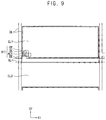
- FIG. 9 is a plan view illustrating one pixel of a display panel according to an exemplary embodiment of the inventive concept.
- the display panel may be substantially same as the display panel of FIG. 6 , except for a third electrode EL 3 .
- a third electrode EL 3 may be substantially same as the display panel of FIG. 6 , except for a third electrode EL 3 .
- the display panel may include a gate line GL, a data line DL, a first electrode EL 1 , the third electrode EL 3 , a thin film transistor TFT, and a second electrode.
- the thin film transistor TFT may include a source electrode SE, an active pattern ACT, a drain electrode DE and a gate electrode GE.
- the gate line GL may extend in a first direction D 1 .
- the gate line GL may be electrically connected to the gate electrode GE of the thin film transistor TFT.
- the data line DL may extend in a second direction D 2 crossing the first direction D 1 .
- the second direction D 2 may be substantially perpendicular to the first direction D 1 .
- the data line DL may be electrically connected to the source electrode SE of the thin film transistor TFT.
- the first electrode EL 1 may be electrically connected to the drain electrode DE of the thin film transistor TFT.
- the first electrode EL 1 may include transparent conductive material.
- the third electrode EL 3 may be spaced apart from the first electrode EL 1 .
- the third electrode EL 3 may be adjacent to the first electrode EL 1 in the second direction D 2 , and extend in the first direction D 1 .
- a portion of the third electrode EL 3 may overlap the data line DL, and extend in the second direction D 2 , so that the third electrode EL 3 may be connected to a third electrode of an adjacent pixel.
- On or off voltage may be applied to the third electrode EL 3 for converting a transparent mode to a normal mode and vise versa.
- the third electrode EL 3 may include transparent conductive material.
- the second electrode may be disposed to face the first electrode EL 1 and the third electrode EL 3 .
- the second electrode may overlap the first and third electrode EL 1 and EL 3 .
- the liquid crystal layer may be disposed between the first electrode EL 1 and the second electrode, and between the third electrode EL 3 and the second electrode.
- FIG. 10 is a plan view illustrating one pixel of a display panel according to an exemplary embodiment of the inventive concept.
- the display panel may be substantially same as the display panel of FIG. 6 , except for a third electrode EL 3 .
- a third electrode EL 3 may be substantially same as the display panel of FIG. 6 , except for a third electrode EL 3 .
- the display panel may include a gate line GL, a data line DL, a first electrode EL 1 , a third electrode EL 3 , a thin film transistor TFT, and a second electrode.
- the thin film transistor TFT may include a source electrode SE, an active pattern ACT, a drain electrode DE and a gate electrode GE.
- the gate line GL may extend in a first direction D 1 .
- the gate line GL may be electrically connected to the gate electrode GE of the thin film transistor TFT.
- the data line DL may extend in a second direction D 2 crossing the first direction D 1 .
- the second direction D 2 may be substantially perpendicular to the first direction D 1 .
- the data line DL may be electrically connected to the source electrode SE of the thin film transistor TFT.
- the first electrode EL 1 may be electrically connected to the drain electrode DE of the thin film transistor TFT.
- the first electrode EL 1 may include transparent conductive material.
- the third electrode EL 3 may be spaced apart from the first electrode EL 1 .
- the third electrode EL 3 may extend in the first direction D 1 and the second direction D 2 to form a mesh structure.
- On or off voltage may be applied to the third electrode EL 3 for converting a transparent mode to a normal mode and vise versa.
- the third electrode EL 3 may include transparent conductive material.
- the second electrode may be disposed to face the first electrode EL 1 and the third electrode EL 3 .
- the second electrode may overlap the first and third electrode EL 1 and EL 3 .
- the liquid crystal layer may be disposed between the first electrode EL 1 and the second electrode, and between the third electrode EL 3 and the second electrode.
- FIGS. 11A to 15B are plan views and cross-sectional views illustrating a method of manufacturing the display panel of FIG. 1 .
- a gate pattern may be formed on a first substrate 100 .
- a conductive layer (not shown) may be formed on the first base substrate 100 , and then the conductive layer may be partially etched by a photolithography process or an etching process using an additional mask. Hence, the gate pattern may be obtained.
- the gate pattern may include a gate line GL, a high storage pattern CSTh and a low storage pattern CSTl.
- the gate line GL may be extended in a first direction D 1 .
- the gate line GL may be electrically connected to a first gate electrode (refers to GE 1 of FIG. 11B ).
- the first gate electrode GE 1 may be a portion of the gate line GL.
- the gate line GL may be electrically connected to a second gate electrode and a third gate electrode.
- the second gate electrode and the third gate electrode may be a portion of the gate line GL.
- the high storage pattern CSTh may extend in the first direction D 1 .
- the high storage pattern CSTh may be electrically connected to a high storage pattern of an adjacent pixel in the first direction D 1 .
- the low storage pattern CSTl may extend in the first direction D 1 .
- the low storage pattern CSTl may be electrically connected to a low storage pattern of the adjacent pixel in the first direction D 1 .
- the gate line GL may be formed between the high storage pattern CSTh and the low storage pattern CSTl.
- the first insulation layer 110 may be formed on the first base substrate 100 on which the gate line GL, the high storage pattern CSTh and the low storage pattern CSTl are formed.
- the first insulation layer 110 may be formed by a spin coating process, a chemical vapor deposition (CVD) process, a plasma enhanced chemical vapor deposition (PECVD) process, a high density plasma-chemical vapor deposition (HDP-CVD) process, and etc.
- An active pattern and a data pattern may be formed on the first insulation layer 110 .
- An active layer (not shown) may be formed on the first insulation layer 110 , and then a conductive layer may be formed on the active layer. And then, the active layer and the conductive layer may be simultaneously patterned to form the active pattern and the data pattern.
- the active layer may include a semiconductor layer consisting of amorphous silicon (a-Si:H) and an ohmic contact layer consisting of n+ amorphous silicon (n+ a-Si:H).
- the active pattern may include an oxide semiconductor.
- the oxide semiconductor may include an amorphous oxide including at least one selected from the group consisting of indium (In), zinc (Zn), gallium (Ga), tin (Sn) and hafnium (Hf).
- the active pattern may include a first active area ACT 1 , a second active area ACT 2 , and a third active area ACT 3 .
- the data pattern may include a data line DL, a first source electrode SE 1 , a first drain electrode DE 1 , a second source electrode SE 2 , a second drain electrode DE 2 , a third source electrode SE 3 , a third drain electrode DE 3 and a voltage dividing reference voltage line RDL.
- the data line DL may extend in a second direction D 2 which crosses the first direction D 1 .
- the second direction D 2 may be substantially perpendicular to the first direction D 1 .
- the data line DL may be electrically connected to the first source electrode SE 1 and the second source electrode SE 2 .
- the first source electrode SE 1 may be electrically connected to the first active area ACT 1 .
- the first drain electrode DE 1 may be spaced apart from the first source electrode SE 1 and electrically connected to the first active area ACT 1 .
- the second source electrode SE 2 may be electrically connected to the second active area ACT 2 .
- the second drain electrode DE 2 may be spaced apart from the second source electrode SE 2 and electrically connected to the second active area ACT 2 .
- the voltage dividing reference voltage line RDL may be spaced apart from the data line DL in the first direction D 1 , and extend in the second direction D 2 .
- the voltage dividing reference voltage line RDL may be electrically connected to the third drain electrode DE 3 .
- the third drain electrode DE 3 may be electrically connected to the third active area ACT 3 .
- the third source electrode SE 3 may be spaced apart from the third drain electrode DE 3 and electrically connected to the third active area ACT 3 .
- the third source electrode SE 3 may be electrically connected to the second drain electrode DE 2 .
- a second insulation layer 120 may be formed on the first insulation layer 110 on which the data line DL and the voltage dividing reference voltage line RDL are formed.
- the second insulation layer 120 may be formed by a spin coating process, a printing process, a sputtering process, a CVD process, an ALD process, a PECVD process, an HDP-CVD process or a vacuum evaporation process in accordance with ingredients included in the second insulation layer 120 .
- Contact holes which expose the data pattern may be formed through the second insulation layer 120 .
- the contact holes which extend to and expose the first and second drain electrodes DE 1 , DE 2 of the first and second thin film transistor TFT 1 and TFT 2 may be formed by partially etching the second insulation layer 120 by a photolithography process or an etching process using an additional mask.
- a pixel electrode pattern may be formed on the second insulation layer 120 .
- the pixel electrode pattern may be filled in the contact holes, and formed on the second insulation layer 120 .
- the pixel electrode pattern may include a first high electrode EL 1 h , a first low electrode EL 1 l , and a third electrode EL 3 .
- a pixel electrode layer may be formed on the second insulation layer 120 , and then the pixel electrode layer may be partially etched by a photolithography process or an etching process using an additional mask. Hence, the pixel electrode pattern may be obtained.
- the pixel electrode layer may be formed by a printing process, a sputtering process, a CVD process, an ALD process, a vacuum evaporation process, a pulsed laser deposition process, and etc.
- the first high electrode EL 1 h may be electrically connected to the first drain electrode DE 1 of the first thin film transistor TFT 1 through the contact hole.
- a boundary of the first high electrode EL 1 h may be overlapped with a portion of the high storage pattern CSTh.
- the first low electrode EL 1 l may be spaced apart from the first high electrode EL 1 h in the second direction D 2 .
- the first low electrode EL 1 l may be electrically connected to the second drain electrode DE 2 of the second thin film transistor TFT 2 and the third source electrode SE 3 of the third thin film transistor TFT 3 through the contact hole.
- a boundary of the first low electrode EL 1 l may be overlapped with a portion of the low storage pattern CSTl.
- the third electrode EL 3 may be spaced apart from the first high electrode EL 1 h and the first low electrode EL 1 l in the first direction D 1 .
- the third electrode EL 3 may be extended in the second direction D 2 .
- the third electrode EL 3 may overlap the voltage dividing reference voltage line RDL and a data line of an adjacent pixel.
- the third electrode EL 3 may be extended in the first direction D 1 , and electrically connected to a third electrode of the adjacent pixel through a connecting electrode EL 3 a which is disposed between the first high electrode EL 1 h and the first low electrode EL 1 l.
- a light blocking pattern BM may be formed on a second base substrate 200 .
- the light blocking pattern BM may overlap the first to third thin film transistors TFT 1 , TFT 2 and TFT 3 .
- a color filter 210 may be formed on the second base substrate 200 on which the light blocking pattern BM is disposed.
- the color filter 210 may overlap the first electrode EL 1 .
- the color filter 210 may be formed not to overlap the third electrode EL 3 .
- An over-coating layer 220 may be formed on the color filter 210 and the light blocking pattern BM.
- the over-coating layer 220 may flatten, protect and insulate the color filter 210 .
- the over-coating layer 220 may include acrylic-epoxy material.
- the second electrode EL 2 may be formed on the over-coating layer 220 .
- the second electrode EL 2 may be formed on the entire second base substrate 200 .
- a liquid crystal layer 300 may be formed between the first high and first low electrode and the third electrodes EL 1 h , EL 1 l and EL 3 and the second electrode EL 2 . Accordingly, the display panel may be manufactured.
- a display panel includes a first electrode, a second electrode, a third electrode and a liquid crystal layer to embody a transparent mode and a normal mode.
- a transparent mode an on voltage is applied to the third electrode, and a common voltage is applied to the second electrode. Accordingly, the liquid crystal layer passes light, so that the display panel can work as a transparent display.
- the normal mode an off voltage is applied to the third electrode, and the common voltage is applied to the second electrode. Accordingly, the liquid crystal layer blocks light, so that the display panel can work as a traditional display.
- the display panel may minimize size of a light blocking pattern, and may improve transparency of the display panel by designing a shape of the third electrode.
- the transparency may be controlled by adjusting voltage level applied to the third electrode.
Landscapes
- Physics & Mathematics (AREA)
- Nonlinear Science (AREA)
- Chemical & Material Sciences (AREA)
- Crystallography & Structural Chemistry (AREA)
- General Physics & Mathematics (AREA)
- Optics & Photonics (AREA)
- Mathematical Physics (AREA)
- Engineering & Computer Science (AREA)
- Microelectronics & Electronic Packaging (AREA)
- Geometry (AREA)
- Liquid Crystal (AREA)
- Devices For Indicating Variable Information By Combining Individual Elements (AREA)
Abstract
Description
Claims (19)
Applications Claiming Priority (2)
| Application Number | Priority Date | Filing Date | Title |
|---|---|---|---|
| KR1020160003346A KR102501976B1 (en) | 2016-01-11 | 2016-01-11 | Display panel and method of manufacturing the same |
| KR10-2016-0003346 | 2016-01-11 |
Publications (2)
| Publication Number | Publication Date |
|---|---|
| US20170199440A1 US20170199440A1 (en) | 2017-07-13 |
| US10690979B2 true US10690979B2 (en) | 2020-06-23 |
Family
ID=59275661
Family Applications (1)
| Application Number | Title | Priority Date | Filing Date |
|---|---|---|---|
| US15/278,915 Expired - Fee Related US10690979B2 (en) | 2016-01-11 | 2016-09-28 | Display panel and method of manufacturing the same |
Country Status (2)
| Country | Link |
|---|---|
| US (1) | US10690979B2 (en) |
| KR (1) | KR102501976B1 (en) |
Families Citing this family (1)
| Publication number | Priority date | Publication date | Assignee | Title |
|---|---|---|---|---|
| KR102707527B1 (en) * | 2019-11-13 | 2024-09-23 | 삼성디스플레이 주식회사 | Display device and fabricating method for display device |
Citations (1)
| Publication number | Priority date | Publication date | Assignee | Title |
|---|---|---|---|---|
| JP2010096974A (en) | 2008-10-16 | 2010-04-30 | Sharp Corp | Transmissive liquid crystal display device |
Family Cites Families (2)
| Publication number | Priority date | Publication date | Assignee | Title |
|---|---|---|---|---|
| JP4361844B2 (en) * | 2004-07-28 | 2009-11-11 | 富士通株式会社 | Liquid crystal display |
| KR101791201B1 (en) * | 2010-12-28 | 2017-10-30 | 삼성디스플레이 주식회사 | Liquid crystal display and method of manufacturing the same |
-
2016
- 2016-01-11 KR KR1020160003346A patent/KR102501976B1/en active Active
- 2016-09-28 US US15/278,915 patent/US10690979B2/en not_active Expired - Fee Related
Patent Citations (1)
| Publication number | Priority date | Publication date | Assignee | Title |
|---|---|---|---|---|
| JP2010096974A (en) | 2008-10-16 | 2010-04-30 | Sharp Corp | Transmissive liquid crystal display device |
Also Published As
| Publication number | Publication date |
|---|---|
| US20170199440A1 (en) | 2017-07-13 |
| KR20170084417A (en) | 2017-07-20 |
| KR102501976B1 (en) | 2023-02-22 |
Similar Documents
| Publication | Publication Date | Title |
|---|---|---|
| US10948789B2 (en) | Display apparatus comprising a bridge portion formed of a same material as a second color filter and connecting adjacent second color filters of adjacent pixel areas | |
| JP6725317B2 (en) | Display device | |
| US9853067B2 (en) | Thin film transistor array substrate | |
| US9324736B2 (en) | Thin film transistor substrate having metal oxide semiconductor and manufacturing the same | |
| US9519182B2 (en) | Display panel and method of manufacturing the same | |
| US9865623B2 (en) | Array substrate and manufacturing method thereof, and display device | |
| KR20180076661A (en) | Substrate for display and display including the same | |
| KR101969568B1 (en) | Thin Film Transistor Substrate Having Oxide Semiconductor and Manufacturing Method Thereof | |
| US10825840B2 (en) | Thin-film transistor panel | |
| US9733520B2 (en) | Display panel and method of manufacturing the same | |
| US9570481B2 (en) | Display substrate and method of manufacturing the same | |
| US10845639B2 (en) | Display device | |
| US10631417B2 (en) | Display apparatus and method of manufacturing the same | |
| US12171122B2 (en) | Display panel and display apparatus including the same | |
| US10243010B2 (en) | Semiconductor substrate and display device | |
| KR20040031370A (en) | Liquid Crystal Display Panel And Fabricating Method Thereof | |
| US10396105B2 (en) | Display substrate and method of manufacturing the same | |
| US10690979B2 (en) | Display panel and method of manufacturing the same | |
| TWI690758B (en) | Liquid crystal display devices with electrode stacks | |
| JP2007180511A (en) | Thin film transistor substrate, manufacturing method thereof, and display panel having the same | |
| US9405163B2 (en) | Thin film transistor substrate and display panel having the same | |
| KR20190081852A (en) | Array substrate for display device and method of manufacturing the same | |
| KR102569742B1 (en) | Electroluminescence light emitting display device and method of manufacturing the same | |
| KR20170015830A (en) | Transparent display device and method for fabricating thereof | |
| KR20060008122A (en) | Liquid crystal display panel and manufacturing method thereof |
Legal Events
| Date | Code | Title | Description |
|---|---|---|---|
| AS | Assignment |
Owner name: SAMSUNG DISPLAY CO., LTD., KOREA, REPUBLIC OF Free format text: ASSIGNMENT OF ASSIGNORS INTEREST;ASSIGNORS:IM, WAN-SOON;SONG, YOUNG GOO;YOON, YEO GEON;AND OTHERS;SIGNING DATES FROM 20160813 TO 20160817;REEL/FRAME:039879/0566 |
|
| STPP | Information on status: patent application and granting procedure in general |
Free format text: FINAL REJECTION MAILED |
|
| STPP | Information on status: patent application and granting procedure in general |
Free format text: RESPONSE AFTER FINAL ACTION FORWARDED TO EXAMINER |
|
| STPP | Information on status: patent application and granting procedure in general |
Free format text: ADVISORY ACTION MAILED |
|
| STPP | Information on status: patent application and granting procedure in general |
Free format text: NON FINAL ACTION MAILED |
|
| STPP | Information on status: patent application and granting procedure in general |
Free format text: RESPONSE TO NON-FINAL OFFICE ACTION ENTERED AND FORWARDED TO EXAMINER |
|
| STPP | Information on status: patent application and granting procedure in general |
Free format text: NOTICE OF ALLOWANCE MAILED -- APPLICATION RECEIVED IN OFFICE OF PUBLICATIONS |
|
| ZAAA | Notice of allowance and fees due |
Free format text: ORIGINAL CODE: NOA |
|
| ZAAB | Notice of allowance mailed |
Free format text: ORIGINAL CODE: MN/=. |
|
| STPP | Information on status: patent application and granting procedure in general |
Free format text: AWAITING TC RESP., ISSUE FEE NOT PAID |
|
| ZAAA | Notice of allowance and fees due |
Free format text: ORIGINAL CODE: NOA |
|
| STPP | Information on status: patent application and granting procedure in general |
Free format text: AWAITING TC RESP, ISSUE FEE PAYMENT RECEIVED |
|
| ZAAA | Notice of allowance and fees due |
Free format text: ORIGINAL CODE: NOA |
|
| STCF | Information on status: patent grant |
Free format text: PATENTED CASE |
|
| FEPP | Fee payment procedure |
Free format text: MAINTENANCE FEE REMINDER MAILED (ORIGINAL EVENT CODE: REM.); ENTITY STATUS OF PATENT OWNER: LARGE ENTITY |
|
| LAPS | Lapse for failure to pay maintenance fees |
Free format text: PATENT EXPIRED FOR FAILURE TO PAY MAINTENANCE FEES (ORIGINAL EVENT CODE: EXP.); ENTITY STATUS OF PATENT OWNER: LARGE ENTITY |
|
| STCH | Information on status: patent discontinuation |
Free format text: PATENT EXPIRED DUE TO NONPAYMENT OF MAINTENANCE FEES UNDER 37 CFR 1.362 |
|
| FP | Lapsed due to failure to pay maintenance fee |
Effective date: 20240623 |