US10690596B2 - Surface plasmon-enhanced fluorescence measurement device and surface plasmon-enhanced fluorescence measurement method - Google Patents
Surface plasmon-enhanced fluorescence measurement device and surface plasmon-enhanced fluorescence measurement method Download PDFInfo
- Publication number
- US10690596B2 US10690596B2 US15/536,109 US201515536109A US10690596B2 US 10690596 B2 US10690596 B2 US 10690596B2 US 201515536109 A US201515536109 A US 201515536109A US 10690596 B2 US10690596 B2 US 10690596B2
- Authority
- US
- United States
- Prior art keywords
- light
- angle
- diffraction grating
- relative
- metal film
- Prior art date
- Legal status (The legal status is an assumption and is not a legal conclusion. Google has not performed a legal analysis and makes no representation as to the accuracy of the status listed.)
- Active, expires
Links
- 238000005259 measurement Methods 0.000 title claims abstract description 56
- 238000000691 measurement method Methods 0.000 title claims description 23
- 230000005284 excitation Effects 0.000 claims abstract description 164
- 239000000126 substance Substances 0.000 claims abstract description 89
- 238000001514 detection method Methods 0.000 claims abstract description 62
- 230000003287 optical effect Effects 0.000 claims abstract description 45
- 230000010287 polarization Effects 0.000 claims abstract description 32
- 229910052751 metal Inorganic materials 0.000 claims description 126
- 239000002184 metal Substances 0.000 claims description 126
- 230000005684 electric field Effects 0.000 claims description 107
- 230000010355 oscillation Effects 0.000 claims description 90
- 239000012491 analyte Substances 0.000 claims description 85
- 239000003446 ligand Substances 0.000 claims description 32
- 238000012545 processing Methods 0.000 claims description 18
- 239000007788 liquid Substances 0.000 claims description 15
- 238000002198 surface plasmon resonance spectroscopy Methods 0.000 claims description 9
- 230000001678 irradiating effect Effects 0.000 claims description 8
- 238000002372 labelling Methods 0.000 claims description 3
- 239000000284 extract Substances 0.000 abstract 1
- 238000000034 method Methods 0.000 description 20
- 238000006243 chemical reaction Methods 0.000 description 17
- 238000001917 fluorescence detection Methods 0.000 description 14
- 238000002474 experimental method Methods 0.000 description 12
- 239000000758 substrate Substances 0.000 description 10
- 239000007850 fluorescent dye Substances 0.000 description 9
- 230000000737 periodic effect Effects 0.000 description 9
- 238000005406 washing Methods 0.000 description 7
- 238000001215 fluorescent labelling Methods 0.000 description 6
- 238000010517 secondary reaction Methods 0.000 description 6
- 239000000463 material Substances 0.000 description 5
- 230000008901 benefit Effects 0.000 description 3
- 230000015572 biosynthetic process Effects 0.000 description 3
- 230000008878 coupling Effects 0.000 description 3
- 238000010168 coupling process Methods 0.000 description 3
- 238000005859 coupling reaction Methods 0.000 description 3
- 230000000694 effects Effects 0.000 description 3
- 229920000642 polymer Polymers 0.000 description 3
- 239000013545 self-assembled monolayer Substances 0.000 description 3
- 230000035945 sensitivity Effects 0.000 description 3
- 230000002123 temporal effect Effects 0.000 description 3
- 238000004458 analytical method Methods 0.000 description 2
- 230000008859 change Effects 0.000 description 2
- 238000002073 fluorescence micrograph Methods 0.000 description 2
- 239000003906 humectant Substances 0.000 description 2
- 239000004973 liquid crystal related substance Substances 0.000 description 2
- 229920006254 polymer film Polymers 0.000 description 2
- 102000004169 proteins and genes Human genes 0.000 description 2
- 108090000623 proteins and genes Proteins 0.000 description 2
- 238000012360 testing method Methods 0.000 description 2
- 239000012099 Alexa Fluor family Substances 0.000 description 1
- RYGMFSIKBFXOCR-UHFFFAOYSA-N Copper Chemical compound [Cu] RYGMFSIKBFXOCR-UHFFFAOYSA-N 0.000 description 1
- 102000004190 Enzymes Human genes 0.000 description 1
- 108090000790 Enzymes Proteins 0.000 description 1
- 241000032989 Ipomoea lacunosa Species 0.000 description 1
- 102000015636 Oligopeptides Human genes 0.000 description 1
- 108010038807 Oligopeptides Proteins 0.000 description 1
- 239000002202 Polyethylene glycol Substances 0.000 description 1
- 239000004793 Polystyrene Substances 0.000 description 1
- BQCADISMDOOEFD-UHFFFAOYSA-N Silver Chemical compound [Ag] BQCADISMDOOEFD-UHFFFAOYSA-N 0.000 description 1
- -1 aliphatic thiol Chemical class 0.000 description 1
- 239000000956 alloy Substances 0.000 description 1
- 229910045601 alloy Inorganic materials 0.000 description 1
- 229910052782 aluminium Inorganic materials 0.000 description 1
- XAGFODPZIPBFFR-UHFFFAOYSA-N aluminium Chemical compound [Al] XAGFODPZIPBFFR-UHFFFAOYSA-N 0.000 description 1
- 150000001413 amino acids Chemical class 0.000 description 1
- 210000004369 blood Anatomy 0.000 description 1
- 239000008280 blood Substances 0.000 description 1
- 210000001124 body fluid Anatomy 0.000 description 1
- 150000001720 carbohydrates Chemical class 0.000 description 1
- 229910052802 copper Inorganic materials 0.000 description 1
- 239000010949 copper Substances 0.000 description 1
- 238000011161 development Methods 0.000 description 1
- 238000005516 engineering process Methods 0.000 description 1
- 238000001506 fluorescence spectroscopy Methods 0.000 description 1
- 239000012634 fragment Substances 0.000 description 1
- 125000000524 functional group Chemical group 0.000 description 1
- 239000011521 glass Substances 0.000 description 1
- PCHJSUWPFVWCPO-UHFFFAOYSA-N gold Chemical compound [Au] PCHJSUWPFVWCPO-UHFFFAOYSA-N 0.000 description 1
- 229910052737 gold Inorganic materials 0.000 description 1
- 239000010931 gold Substances 0.000 description 1
- 238000003018 immunoassay Methods 0.000 description 1
- 230000006872 improvement Effects 0.000 description 1
- 229910010272 inorganic material Inorganic materials 0.000 description 1
- 239000011147 inorganic material Substances 0.000 description 1
- 150000002632 lipids Chemical class 0.000 description 1
- QSHDDOUJBYECFT-UHFFFAOYSA-N mercury Chemical compound [Hg] QSHDDOUJBYECFT-UHFFFAOYSA-N 0.000 description 1
- 229910052753 mercury Inorganic materials 0.000 description 1
- 150000002739 metals Chemical class 0.000 description 1
- 210000003097 mucus Anatomy 0.000 description 1
- 230000007935 neutral effect Effects 0.000 description 1
- 102000039446 nucleic acids Human genes 0.000 description 1
- 108020004707 nucleic acids Proteins 0.000 description 1
- 150000007523 nucleic acids Chemical class 0.000 description 1
- NRNCYVBFPDDJNE-UHFFFAOYSA-N pemoline Chemical compound O1C(N)=NC(=O)C1C1=CC=CC=C1 NRNCYVBFPDDJNE-UHFFFAOYSA-N 0.000 description 1
- 210000002381 plasma Anatomy 0.000 description 1
- 238000007747 plating Methods 0.000 description 1
- 229920003229 poly(methyl methacrylate) Polymers 0.000 description 1
- 239000004417 polycarbonate Substances 0.000 description 1
- 229920000515 polycarbonate Polymers 0.000 description 1
- 229920001223 polyethylene glycol Polymers 0.000 description 1
- 239000004926 polymethyl methacrylate Substances 0.000 description 1
- 229920000098 polyolefin Polymers 0.000 description 1
- 229920001184 polypeptide Polymers 0.000 description 1
- 229920002223 polystyrene Polymers 0.000 description 1
- 230000008569 process Effects 0.000 description 1
- 102000004196 processed proteins & peptides Human genes 0.000 description 1
- 108090000765 processed proteins & peptides Proteins 0.000 description 1
- 239000010453 quartz Substances 0.000 description 1
- 239000011347 resin Substances 0.000 description 1
- 229920005989 resin Polymers 0.000 description 1
- 210000003296 saliva Anatomy 0.000 description 1
- 239000002094 self assembled monolayer Substances 0.000 description 1
- 210000000582 semen Anatomy 0.000 description 1
- 210000002966 serum Anatomy 0.000 description 1
- 229910052710 silicon Inorganic materials 0.000 description 1
- 239000010703 silicon Substances 0.000 description 1
- VYPSYNLAJGMNEJ-UHFFFAOYSA-N silicon dioxide Inorganic materials O=[Si]=O VYPSYNLAJGMNEJ-UHFFFAOYSA-N 0.000 description 1
- 229910052709 silver Inorganic materials 0.000 description 1
- 239000004332 silver Substances 0.000 description 1
- 238000004544 sputter deposition Methods 0.000 description 1
- 238000012546 transfer Methods 0.000 description 1
- 210000002700 urine Anatomy 0.000 description 1
- 238000007740 vapor deposition Methods 0.000 description 1
Images


Classifications
-
- G—PHYSICS
- G01—MEASURING; TESTING
- G01N—INVESTIGATING OR ANALYSING MATERIALS BY DETERMINING THEIR CHEMICAL OR PHYSICAL PROPERTIES
- G01N21/00—Investigating or analysing materials by the use of optical means, i.e. using sub-millimetre waves, infrared, visible or ultraviolet light
- G01N21/62—Systems in which the material investigated is excited whereby it emits light or causes a change in wavelength of the incident light
- G01N21/63—Systems in which the material investigated is excited whereby it emits light or causes a change in wavelength of the incident light optically excited
- G01N21/64—Fluorescence; Phosphorescence
- G01N21/645—Specially adapted constructive features of fluorimeters
- G01N21/648—Specially adapted constructive features of fluorimeters using evanescent coupling or surface plasmon coupling for the excitation of fluorescence
-
- G—PHYSICS
- G01—MEASURING; TESTING
- G01J—MEASUREMENT OF INTENSITY, VELOCITY, SPECTRAL CONTENT, POLARISATION, PHASE OR PULSE CHARACTERISTICS OF INFRARED, VISIBLE OR ULTRAVIOLET LIGHT; COLORIMETRY; RADIATION PYROMETRY
- G01J3/00—Spectrometry; Spectrophotometry; Monochromators; Measuring colours
- G01J3/02—Details
- G01J3/0202—Mechanical elements; Supports for optical elements
-
- G—PHYSICS
- G01—MEASURING; TESTING
- G01J—MEASUREMENT OF INTENSITY, VELOCITY, SPECTRAL CONTENT, POLARISATION, PHASE OR PULSE CHARACTERISTICS OF INFRARED, VISIBLE OR ULTRAVIOLET LIGHT; COLORIMETRY; RADIATION PYROMETRY
- G01J3/00—Spectrometry; Spectrophotometry; Monochromators; Measuring colours
- G01J3/02—Details
- G01J3/0205—Optical elements not provided otherwise, e.g. optical manifolds, diffusers, windows
- G01J3/0224—Optical elements not provided otherwise, e.g. optical manifolds, diffusers, windows using polarising or depolarising elements
-
- G—PHYSICS
- G01—MEASURING; TESTING
- G01J—MEASUREMENT OF INTENSITY, VELOCITY, SPECTRAL CONTENT, POLARISATION, PHASE OR PULSE CHARACTERISTICS OF INFRARED, VISIBLE OR ULTRAVIOLET LIGHT; COLORIMETRY; RADIATION PYROMETRY
- G01J3/00—Spectrometry; Spectrophotometry; Monochromators; Measuring colours
- G01J3/02—Details
- G01J3/0205—Optical elements not provided otherwise, e.g. optical manifolds, diffusers, windows
- G01J3/0237—Adjustable, e.g. focussing
-
- G—PHYSICS
- G01—MEASURING; TESTING
- G01J—MEASUREMENT OF INTENSITY, VELOCITY, SPECTRAL CONTENT, POLARISATION, PHASE OR PULSE CHARACTERISTICS OF INFRARED, VISIBLE OR ULTRAVIOLET LIGHT; COLORIMETRY; RADIATION PYROMETRY
- G01J3/00—Spectrometry; Spectrophotometry; Monochromators; Measuring colours
- G01J3/12—Generating the spectrum; Monochromators
- G01J3/18—Generating the spectrum; Monochromators using diffraction elements, e.g. grating
-
- G—PHYSICS
- G01—MEASURING; TESTING
- G01N—INVESTIGATING OR ANALYSING MATERIALS BY DETERMINING THEIR CHEMICAL OR PHYSICAL PROPERTIES
- G01N21/00—Investigating or analysing materials by the use of optical means, i.e. using sub-millimetre waves, infrared, visible or ultraviolet light
- G01N21/62—Systems in which the material investigated is excited whereby it emits light or causes a change in wavelength of the incident light
- G01N21/63—Systems in which the material investigated is excited whereby it emits light or causes a change in wavelength of the incident light optically excited
- G01N21/64—Fluorescence; Phosphorescence
- G01N21/6428—Measuring fluorescence of fluorescent products of reactions or of fluorochrome labelled reactive substances, e.g. measuring quenching effects, using measuring "optrodes"
-
- G—PHYSICS
- G01—MEASURING; TESTING
- G01N—INVESTIGATING OR ANALYSING MATERIALS BY DETERMINING THEIR CHEMICAL OR PHYSICAL PROPERTIES
- G01N21/00—Investigating or analysing materials by the use of optical means, i.e. using sub-millimetre waves, infrared, visible or ultraviolet light
- G01N21/62—Systems in which the material investigated is excited whereby it emits light or causes a change in wavelength of the incident light
- G01N21/63—Systems in which the material investigated is excited whereby it emits light or causes a change in wavelength of the incident light optically excited
- G01N21/64—Fluorescence; Phosphorescence
- G01N21/6445—Measuring fluorescence polarisation
-
- G—PHYSICS
- G01—MEASURING; TESTING
- G01N—INVESTIGATING OR ANALYSING MATERIALS BY DETERMINING THEIR CHEMICAL OR PHYSICAL PROPERTIES
- G01N33/00—Investigating or analysing materials by specific methods not covered by groups G01N1/00 - G01N31/00
- G01N33/48—Biological material, e.g. blood, urine; Haemocytometers
- G01N33/50—Chemical analysis of biological material, e.g. blood, urine; Testing involving biospecific ligand binding methods; Immunological testing
- G01N33/53—Immunoassay; Biospecific binding assay; Materials therefor
- G01N33/543—Immunoassay; Biospecific binding assay; Materials therefor with an insoluble carrier for immobilising immunochemicals
- G01N33/54366—Apparatus specially adapted for solid-phase testing
- G01N33/54373—Apparatus specially adapted for solid-phase testing involving physiochemical end-point determination, e.g. wave-guides, FETS, gratings
-
- G—PHYSICS
- G01—MEASURING; TESTING
- G01N—INVESTIGATING OR ANALYSING MATERIALS BY DETERMINING THEIR CHEMICAL OR PHYSICAL PROPERTIES
- G01N33/00—Investigating or analysing materials by specific methods not covered by groups G01N1/00 - G01N31/00
- G01N33/48—Biological material, e.g. blood, urine; Haemocytometers
- G01N33/50—Chemical analysis of biological material, e.g. blood, urine; Testing involving biospecific ligand binding methods; Immunological testing
- G01N33/53—Immunoassay; Biospecific binding assay; Materials therefor
- G01N33/543—Immunoassay; Biospecific binding assay; Materials therefor with an insoluble carrier for immobilising immunochemicals
- G01N33/551—Immunoassay; Biospecific binding assay; Materials therefor with an insoluble carrier for immobilising immunochemicals the carrier being inorganic
- G01N33/553—Metal or metal coated
-
- G—PHYSICS
- G01—MEASURING; TESTING
- G01N—INVESTIGATING OR ANALYSING MATERIALS BY DETERMINING THEIR CHEMICAL OR PHYSICAL PROPERTIES
- G01N21/00—Investigating or analysing materials by the use of optical means, i.e. using sub-millimetre waves, infrared, visible or ultraviolet light
- G01N21/62—Systems in which the material investigated is excited whereby it emits light or causes a change in wavelength of the incident light
- G01N21/63—Systems in which the material investigated is excited whereby it emits light or causes a change in wavelength of the incident light optically excited
- G01N21/64—Fluorescence; Phosphorescence
- G01N21/6428—Measuring fluorescence of fluorescent products of reactions or of fluorochrome labelled reactive substances, e.g. measuring quenching effects, using measuring "optrodes"
- G01N2021/6439—Measuring fluorescence of fluorescent products of reactions or of fluorochrome labelled reactive substances, e.g. measuring quenching effects, using measuring "optrodes" with indicators, stains, dyes, tags, labels, marks
-
- G—PHYSICS
- G01—MEASURING; TESTING
- G01N—INVESTIGATING OR ANALYSING MATERIALS BY DETERMINING THEIR CHEMICAL OR PHYSICAL PROPERTIES
- G01N21/00—Investigating or analysing materials by the use of optical means, i.e. using sub-millimetre waves, infrared, visible or ultraviolet light
- G01N21/62—Systems in which the material investigated is excited whereby it emits light or causes a change in wavelength of the incident light
- G01N21/63—Systems in which the material investigated is excited whereby it emits light or causes a change in wavelength of the incident light optically excited
- G01N21/64—Fluorescence; Phosphorescence
- G01N21/645—Specially adapted constructive features of fluorimeters
- G01N2021/6463—Optics
-
- G—PHYSICS
- G01—MEASURING; TESTING
- G01N—INVESTIGATING OR ANALYSING MATERIALS BY DETERMINING THEIR CHEMICAL OR PHYSICAL PROPERTIES
- G01N2201/00—Features of devices classified in G01N21/00
- G01N2201/06—Illumination; Optics
- G01N2201/068—Optics, miscellaneous
- G01N2201/0683—Brewster plate; polarisation controlling elements
Definitions
- the present invention relates to a surface plasmon-field enhanced fluorescence measurement apparatus and a surface plasmon-field enhanced fluorescence measurement method for detecting, utilizing surface plasmon resonance, the presence or an amount of an analyte contained in a sample.
- SPFS surface plasmon-field enhanced fluorescence spectroscopy
- SPR surface plasmon resonance
- a ligand e.g., primary antibody
- a ligand that can specifically bind to an analyte is immobilized above a metal film, thereby forming a reaction site for specifically capturing an analyte.
- the analyte bound to the reaction site is labeled with the fluorescent substance.
- the fluorescent substance that labels the analyte is excited by enhanced electric fields due to SPR to emit fluorescence.
- the presence or an amount of the analyte can be detected by detecting fluorescence.
- SPFS can detect an analyte highly sensitively since a fluorescent substance is excited by enhanced electric fields due to SPR.
- SPFS is broadly categorized into prism coupling (PC)-SPFS and grating coupling (GC)-SPFS in accordance with a means for coupling excitation light and surface plasmon.
- PC-SPFS utilizes a prism formed on one surface of a metal film. In this method, excitation light and surface plasmon are coupled by total reflection of excitation light at an interface between the prism and the metal film.
- PC-SPFS which is a mainstream method today, has a challenge of downsizing a measurement apparatus since a prism is used and an incident angle of excitation light on a metal film is large.
- GC-SPFS couples excitation light and surface plasmon utilizing a diffraction grating (see Patent Literature (hereinafter abbreviated as PTL) 1 and Non-Patent Literature (hereinafter abbreviated as NPL) 1).
- PTL Patent Literature
- NPL Non-Patent Literature
- GC-SPFS can downsize a measurement apparatus compared with PC-SPFS, since a prism is not used and an incident angle of excitation light on a diffraction grating is small.
- GC-SPFS has the advantage that a measurement apparatus can be downsized compared with PC-SPFS
- GC-SPFS has not yet been vigorously studied compared with PC-SPFS. Accordingly, a measurement apparatus and a measurement method utilizing GC-SPFS have room for improvement in detection sensitivity.
- An object of the present invention is to provide a measurement apparatus and a measurement method utilizing GC-SPFS that can detect an analyte with higher sensitively.
- a surface plasmon-field enhanced fluorescence measurement apparatus configured to be equipped with a chip which includes a metal film where a diffraction grating is formed and which includes a ligand, for capturing an analyte to be labeled with a fluorescent substance, immobilized above the diffraction grating, and configured to detect the presence or an amount of the analyte by irradiating the diffraction grating with excitation light
- the measurement apparatus includes: a light source configured to irradiate the diffraction grating with linearly polarized excitation light so that the fluorescent substance is excited by an enhanced electric field to emit fluorescence; a rotation section configured to change a direction of an optical axis of the excitation light relative to the diffraction grating in a plan view, or change a polarization direction of the excitation light relative to the diffraction grating; a polarizer
- a surface plasmon-field enhanced fluorescence measurement method for detecting fluorescence emitted from a fluorescent substance, which labels an analyte and is excited by an electric field based on surface plasmon resonance, to detect the presence or an amount of an analyte
- the measurement method includes: a first step of preparing a chip which has a metal film where a diffraction grating is formed and which has a ligand, for capturing an analyte to be labeled with a fluorescent substance, immobilized above the diffraction grating; a second step of irradiating the diffraction grating with linearly polarized excitation light, when a liquid containing the fluorescent substance is present on the metal film, so as to generate surface plasmon resonance in the diffraction grating; detecting linearly polarized first light with an angle of an oscillation direction of an electric field in the range of
- a measurement apparatus and a measurement method utilizing GC-SPFS can detect an analyte with higher sensitively.
- FIG. 1 is a schematic view illustrating a configuration of a surface plasmon-field enhanced fluorescence measurement apparatus (hereinafter referred to as “SPFS apparatus”) according to Embodiment 1;
- SPFS apparatus surface plasmon-field enhanced fluorescence measurement apparatus
- FIGS. 2A and 2B are perspective views of diffraction gratings
- FIG. 3A is a schematic view illustrating a first mode of a chip according to Embodiment 1
- FIG. 3B is a schematic view illustrating a second mode of a chip according to Embodiment 1;
- FIGS. 4A and 4B are schematic views for explaining an incident angle
- FIG. 5 is a flow chart showing the operations of a SPFS apparatus according to Embodiment 1;
- FIGS. 6A and 6B are schematic views illustrating a measurement procedure of fluorescence intensity
- FIG. 7A is a schematic view illustrating a measurement procedure of fluorescence intensity
- FIG. 7B is a view for explaining a measurement principle
- FIG. 8 is a schematic view illustrating a configuration of a SPFS apparatus according to Embodiment 2;
- FIG. 9 is a flow chart showing the operations of a SPFS apparatus according to Embodiment 2.
- FIG. 10 is a schematic view illustrating another example of a configuration of a SPFS apparatus according to Embodiments 1 and 2;
- FIGS. 11A and 11B are schematic views illustrating a procedure of a reference experiment
- FIGS. 12A and 12B are graphs showing measured results of the reference experiment.
- FIGS. 13A and 13B are graphs showing measured results of the reference experiment.
- FIG. 1 is a schematic view illustrating a configuration of a surface plasmon-field enhanced fluorescence measurement apparatus (SPFS apparatus) 100 according to Embodiment 1 of the present invention.
- SPFS apparatus surface plasmon-field enhanced fluorescence measurement apparatus
- SPFS apparatus 100 includes excitation light irradiation unit 110 , rotation section 120 , fluorescence detection unit 130 , and control section 140 .
- SPFS apparatus 100 is used while chip 200 is mounted on chip holder 122 in rotation section 120 . Detection chip 200 will be described first, followed by the description of SPFS apparatus 100 .
- Chip 200 includes substrate 210 and metal film 220 formed on substrate 210 .
- Diffraction grating 230 is formed in metal film 220 .
- a ligand e.g., primary antibody
- a surface of diffraction grating 230 functions as a reaction site for binding a ligand and an analyte.
- a ligand and an analyte are not shown.
- Substrate 210 is a support member for metal film 220 .
- Materials for substrate 210 are not limited as long as they have enough mechanical strength to support metal film 220 .
- Examples of the materials for substrate 210 include inorganic materials, such as glass, quartz, and silicon, and resins, such as polymethyl methacrylate, a polycarbonate, polystyrene, and a polyolefin.
- Metal film 220 is disposed on substrate 210 .
- diffraction grating 230 is formed in metal film 220 .
- surface plasmon generated in metal film 220 and evanescent waves generated by diffraction grating 230 are coupled, thereby generating surface plasmon resonance.
- Materials for metal film 220 are not limited as long as metals can generate surface plasmon.
- Examples of the materials for metal film 220 include gold, silver, copper, aluminum, and an alloy thereof.
- a formation method of metal film 220 is not limited. Examples of the formation methods of metal film 220 include sputtering, vapor deposition, and plating.
- the thickness of metal film 220 is not limited. The thickness of metal film 220 is, for example, 30 to 500 nm, preferably 100 to 300 nm.
- Diffraction grating 230 generates evanescent waves upon irradiation of metal film 220 with light.
- the shape of diffraction grating 230 is not limited as long as evanescent waves can be generated.
- diffraction grating 230 may be a one-dimensional diffraction grating as illustrated in FIG. 2A , or may be a two-dimensional diffraction grating as illustrated in FIG. 2B .
- a plurality of mutually parallel protruded strips are formed at a predetermined pitch on a surface of metal film 220 .
- protruded portions of a predetermined shape are disposed periodically on a surface of metal film 220 .
- Examples of the alignment of the protruded portions include a square lattice and a triangular (hexagonal) lattice.
- Examples of the cross-sectional shapes of diffraction grating 230 include a square waveform, a sinusoidal waveform, and a sawtooth shape.
- a formation method of diffraction grating 230 is not limited. For example, after forming metal film 220 on planar substrate 210 , protruded-recessed shapes may be imparted to metal film 220 . Alternatively, metal film 220 may be formed on substrate 210 in which protruded-recessed shapes are imparted in advance. By either the method, metal film 220 including diffraction grating 230 can be formed.
- a ligand for capturing an analyte is immobilized above diffraction grating 230 (reaction site).
- a ligand specifically binds to an analyte.
- a ligand is almost evenly immobilized above a surface of diffraction grating 230 .
- the type of ligand is not limited as long as an analyte can be captured.
- a ligand is an antibody (e.g., primary antibody) specific to an analyte, a fragment thereof, or an enzyme that can specifically bonds to an analyte.
- An immobilization method of a ligand is not limited.
- a ligand-bound self-assembled monolayer hereinafter referred to as “SAM”
- SAM ligand-bound self-assembled monolayer
- polymer film may be formed above diffraction grating 230 .
- SAM include films formed from a substituted aliphatic thiol, such as HOOC(CH 2 ) 11 SH.
- component materials for the polymer film include polyethylene glycol and MPC polymer.
- a polymer having a reactive group (or a functional group that can be converted into a reactive group) that can bind to a ligand may be immobilized above diffraction grating 230 , followed by binding of a ligand to the polymer.
- metal film 220 (diffraction grating 230 ) is irradiated with excitation light ⁇ at predetermined incident angle ⁇ 1 .
- surface plasmon generated in metal film 220 and evanescent waves generated by diffraction grating 230 are coupled, thereby generating SPR.
- fluorescence ⁇ is emitted.
- fluorescence ⁇ is emitted with directivity in a particular direction. For example, emission angle ⁇ 2 of fluorescence ⁇ is approximated as 2 ⁇ 1 . Reflected light ⁇ of excitation light ⁇ scarcely arises.
- diffraction grating 230 comes into contact with a liquid, such as a buffer, for a reaction, washing, or other operations. Accordingly, diffraction grating 230 is typically disposed in space where a liquid can be housed. As illustrated in FIG. 3A , for example, diffraction grating 230 may be disposed on an inner surface (e.g., bottom surface) of a well, which houses a liquid, or may be disposed on an inner surface (e.g., bottom surface) of a channel (flow cell), which can feed a liquid continuously, as illustrated in FIG. 3B . For example, detection chip 200 illustrated in FIG.
- detection chip 200 illustrated in FIG. 3B is suitable for a reaction constant analysis (real-time measurement) of a molecule (analyte) relative to another molecule (ligand) immobilized above a surface of metal film 220 , as well as a general measurement of an analyte (non-real-time measurement).
- the pitch of diffraction grating 230 is preferably about 400 nm, for example.
- SPFS apparatus 100 includes excitation light irradiation unit 110 , rotation section 120 , fluorescence detection unit 130 , and control section 140 .
- Excitation light irradiation unit 110 irradiates metal film 220 (diffraction grating 230 ) of chip 200 with linearly polarized excitation light ⁇ having a certain wavelength and light quantity. In this step, excitation light irradiation unit 110 irradiates metal film 220 (diffraction grating 230 ) with linearly polarized excitation light ⁇ so as to generate, at diffraction grating 230 , diffracted light that can couple with surface plasmon in metal film 220 .
- the optical axis of excitation light ⁇ is tilted from normal line N to metal film 220 in a side view of chip 200 (see FIG. 4A ). Also, the optical axis of excitation light ⁇ is parallel to or tilted from straight line L along the alignment direction of a periodic structure of diffraction grating 230 (see FIG. 4B ).
- Excitation light irradiation unit 110 includes at least light source 112 and first polarizer 114 . Excitation light irradiation unit 110 may further include a collimator lens, an excitation light filter, or the like.
- Light source 112 emits excitation light ⁇ toward diffraction grating 230 of chip 200 .
- light source 112 is a laser diode.
- the type of light source 112 is not limited, and may not be a laser diode. Examples of light source 112 include a light emitting diode, a mercury lamp, and other laser light sources.
- First polarizer 114 is disposed between light source 112 and diffraction grating 230 , and isolates linearly polarized excitation light ⁇ from excitation light ⁇ emitted from light source 112 .
- the type of first polarizer 114 is not limited as long as linearly polarized excitation light ⁇ with a predetermined polarization direction can be isolated.
- Examples of first polarizer 114 include a polarizing prism, a liquid crystal filter, and other polarizing filters.
- first polarizer 114 is a polarizing plate.
- First polarizer 114 isolates linearly polarized excitation light ⁇ with an angle of an oscillation direction of the electric field in the range of 0 ⁇ 30° relative to a plane containing normal line N to a surface of metal film 220 and an optical axis of excitation light ⁇ (hereinafter referred to as “the plane”) from excitation light ⁇ emitted from light source 112 .
- excitation light filter (not shown) is disposed between light source 112 and chip 200 , and modulates excitation light ⁇ emitted from light source 112 .
- the excitation light filters include a bandpass filter, for example. Since excitation light ⁇ from a laser diode (light source 112 ) has some wavelength distribution widths, a bandpass filter converts excitation light ⁇ into narrow-band light solely composed of the central wavelength.
- a collimator lens (not shown) is disposed between light source 112 and chip 200 , and collimates excitation light ⁇ emitted from light source 112 .
- Excitation light ⁇ emitted from a laser diode (light source 112 ) has a flat contour shape even after collimated. For this reason, the laser diode is held in a predetermined orientation so that the shape of an irradiation spot becomes almost circular on a surface of metal film 220 .
- the size of the irradiation spot is preferably about 1 mm ⁇ , for example.
- Incident angle ⁇ 1 of excitation light ⁇ on metal film 220 can be represented by incident angle ⁇ 1a of excitation light ⁇ in a side view of chip 200 and incident angle ⁇ 1b of excitation light ⁇ in a plan view of chip 200 .
- FIGS. 4A and 4B are schematic views for explaining an incident angle ⁇ 1 ( ⁇ 1a , ⁇ 1b ).
- FIG. 4A is a schematic view for explaining incident angle ⁇ 1a of excitation light ⁇ in a side view of chip 200
- FIG. 4B is a schematic view for explaining incident angle ⁇ 1b of excitation light ⁇ in a plan view of chip 200 .
- x-axis direction is defined as an alignment direction of a periodic structure of diffraction grating 230 , y-axis as an axis perpendicular to x-axis and parallel to a surface of metal film 220 , and z-axis as an axis perpendicular to both x-axis and a surface of metal film 220 .
- the optical axis of excitation light ⁇ is tilted, by a predetermined angle, from normal line N to a surface of metal film 220 in a side view of chip 200 .
- a small angle ⁇ 1a (hereinafter also referred to as “incident angle ⁇ 1a of excitation light ⁇ ”) between the optical axis of excitation light ⁇ and normal line N to a surface of metal film 220 is an angle at which fluorescence ⁇ (enhanced electric fields) becomes most intense.
- Incident angle ⁇ 1a of excitation light ⁇ is appropriately selected in accordance with a pitch of diffraction grating 230 , a wavelength of excitation light ⁇ , the type of a component metal for metal film 220 , or the like. Since an optimal incident angle ⁇ 1a of excitation light ⁇ in a side view of chip 200 varies in accordance with changes in various conditions, SPFS apparatus 100 preferably includes a first angle adjustment section (not shown) configured to adjust incident angle ⁇ 1a by relatively rotating the optical axis of excitation light ⁇ and chip 200 around a straight line (as a central axis), which is positioned on a surface of metal film 220 and passes through an intersection between the optical axis of excitation light ⁇ and metal film 220 (diffraction grating 230 ).
- the first angle adjustment section for example, may mutually rotate excitation light irradiation unit 110 and chip 200 around a straight line on a surface of metal film 220 passing through an intersection between the optical axis of ex
- the optical axis of excitation light ⁇ is parallel to or tilted from straight line L along the alignment direction of a periodic structure of diffraction grating 230 (x-axis direction) in a plan view of chip 200 .
- a small angle ⁇ 1b (hereinafter also referred to as “incident angle ⁇ 1b of excitation light ⁇ ”) between the optical axis of excitation light ⁇ and straight line L along the alignment direction of a periodic structure of diffraction grating 230 is an angle at which a difference value between a detected value of a first light (e.g., light with an angle of an oscillation direction of the electric field of 0° relative to the plane) and a detected value of a second light (e.g., light with an angle of an oscillation direction of the electric field of 90° relative to the plane) becomes zero when a liquid containing a fluorescent substance is present on metal film 220 described below.
- a first light e.g., light with an angle of an oscillation direction of the electric field of 0° relative to the plane
- a detected value of a second light e.g., light with an angle of an oscillation direction of the electric field of 90° relative to the plane
- incident angle ⁇ 1b of excitation light ⁇ in a plan view of chip 200 is not limited.
- incident angle ⁇ 1b of excitation light ⁇ in a plan view of chip 200 is adjusted by rotation section 120 .
- an optimal incident angle ⁇ 1 in a plan view of chip 200 requires the optical axis of excitation light ⁇ to be extended along the alignment direction of a periodic structure of diffraction grating 230 (x-axis direction in FIGS. 2A and 2B ).
- the embodiment sets an angle of the optical axis of excitation light ⁇ relative to straight line L along the alignment direction of a periodic structure of diffraction grating 230 .
- Rotation section 120 changes an optical axis direction (angle) of excitation light ⁇ relative to diffraction grating 230 in a plan view.
- rotation section 120 rotates diffraction grating 230 (chip 200 ) around normal line N (to a surface of metal film 220 ) passing through an intersection between the optical axis of excitation light ⁇ and metal film 220 as a central axis.
- rotation section 120 is not limited as long as an optical axis direction of excitation light ⁇ relative to diffraction grating 230 in a plan view can be changed.
- rotation section 120 includes chip holder 122 and motor 124 .
- the configuration of chip holder 122 is not limited as long as chip 200 can be held.
- chip holder 122 is formed as a box with the top surface opened so that chip 200 can be housed inside.
- Motor 124 rotates chip holder 122 around normal line N as a central axis. Motor 124 is connected to a chip holder 122 , and thus chip 200 is rotated by a predetermined angle by rotating motor 124 .
- Fluorescence detection unit 130 is disposed facing excitation light irradiation unit with normal line N (to a surface of metal film 220 passing through an intersection between the optical axis of excitation light ⁇ and metal film 220 ) therebetween. Fluorescence detection unit 130 detects reflected light ⁇ (of excitation light ⁇ ) reflected on metal film 220 and fluorescence ⁇ emitted from a fluorescent substance above diffraction grating 230 (reaction site).
- Fluorescence detection unit 130 includes at least second polarizer 132 and light detection section 134 . Fluorescence detection unit 130 may further include a condensing lens group, an aperture stop, a fluorescence filter, or the like.
- Second polarizer 132 is disposed between diffraction grating 230 and light detection section 134 , and isolates linearly polarized light from fluorescence ⁇ emitted from a fluorescent substance.
- the type of second polarizer 132 is not limited as long as linearly polarized light with a predetermined polarization direction can be isolated.
- Examples of second polarizer 132 include a polarizing prism, a liquid crystal filter, and other polarizing filters.
- second polarizer 132 is a polarizing plate. Second polarizer 132 is held so that it can rotate in a plane perpendicular to the propagation direction of fluorescence ⁇ toward light detection section 134 from metal film 220 .
- Second polarizer 132 isolates two types of light during determination of incident angle ⁇ 1b of excitation light ⁇ in a plan view of chip 200 and during detection of an analyte. During determination of incident angle ⁇ 1b of excitation light ⁇ , second polarizer 132 isolates, from fluorescence ⁇ emitted from a fluorescent substance when a liquid containing the fluorescent substance is present on metal film 220 , first light with an angle of an oscillation direction of the electric field in the range of 0 ⁇ 30° relative to the plane and second light with an angle of an oscillation direction of the electric field in the range of 90 ⁇ 30° relative to the plane.
- second polarizer 132 isolates, from fluorescence ⁇ , light with an angle of an oscillation direction of the electric field of 0° relative to the plane as a first light and light with an angle of an oscillation direction of the electric field of 90° relative to the plane as a second light.
- second polarizer 132 isolates, from fluorescence ⁇ emitted from a fluorescent substance when an analyte labeled with the fluorescent substance is captured by a ligand, third light with an angle of an oscillation direction of the electric field in the range of 0 ⁇ 30° relative to the plane and fourth light with an angle of an oscillation direction of the electric field in the range of 90 ⁇ 30° relative to the plane.
- second polarizer 132 isolates, from fluorescence ⁇ , light with an angle of an oscillation direction of the electric field of 0° relative to the plane as a third light and light with an angle of an oscillation direction of the electric field of 90° relative to the plane as a fourth light.
- the first light or the second light is isolated by rotating second polarizer (polarizing plate) 132 .
- the third light or the fourth light is isolated by rotating second polarizer (polarizing plate) 132 .
- Light detection section 134 detects linearly polarized light isolated by second polarizer 132 to detect a fluorescence image above metal film 220 .
- light detection section 134 detects the first light or the second light.
- light detection section 134 detects the third light or the fourth light.
- Light detection section 134 is, for example, a photomultiplier tube with high sensitivity and a high S/N ratio.
- Light detection section 134 may be an avalanche photodiode (APD), a photodiode (PD), a CCD image sensor, or the like.
- a condensing lens group (not shown) is disposed between chip 200 and light detection section 134 , and constitutes a conjugate optical system insusceptible to stray light.
- a condensing lens group images, on light receiving surface of light detection section 134 , a fluorescence image above metal film 220 .
- a fluorescence filter (not shown) is disposed between chip 200 and light detection section 134 .
- the fluorescence filters which include a cutoff filter and a neutral density (ND) filter, eliminate noise component (e.g., excitation light ⁇ and extraneous light), which is light that reaches light detection section 134 excluding fluorescence ⁇ , and adjust light quantity of light that reaches light detection section 134 .
- noise component e.g., excitation light ⁇ and extraneous light
- an optical axis angle of fluorescence detection unit 130 relative to normal line N to a surface of metal film 220 is preferably an angle at which the intensity of fluorescence ⁇ is maximum (fluorescence peak angle).
- SPFS apparatus 100 preferably includes a second angle adjustment section (not shown) configured to adjust an optical axis angle of fluorescence detection unit 130 by relatively rotating the optical axis of fluorescence detection unit 130 and chip 200 .
- the second angle adjustment section may mutually rotate fluorescence detection unit 130 and chip 200 around a straight line on a surface of metal film 220 passing through an intersection between the optical axis of fluorescence detection unit 130 and metal film 220 .
- Control section 140 controls the operations of excitation light irradiation unit 110 (light source 112 , first polarizer 114 , and first angle adjustment section), rotation section 120 (motor 124 ), and fluorescence detection unit 130 (second polarizer 132 , light detection section 134 , and second angle adjustment section). Control section 140 also functions as a processing section that processes output signals (detected results) from light detection section 134 . Control section 140 is a computer that executes software, for example.
- FIG. 5 is a flow chart showing an example of an operational procedure of SPFS apparatus 100 .
- FIGS. 6A, 6B, and 7A are schematic views illustrating a measurement procedure of fluorescence intensity.
- FIG. 7B is a view for explaining a measurement principle.
- a primary antibody as a ligand is immobilized above metal film 220 .
- a secondary antibody labeled with a fluorescent substance is used as a ligand for fluorescent labeling.
- the measurement is prepared (step S 10 ). Specifically, chip 200 is prepared, and then chip 200 is installed in chip holder 122 . When a humectant is present above/on metal film 220 of chip 200 , the humectant is removed by washing above/on metal film 220 so that a primary antibody properly captures an analyte.
- Control section 140 determines incident angle ⁇ 1a of excitation light ⁇ in a side view of chip 200 (step S 20 ). Specifically, as illustrated in FIG. 6A , control section 140 irradiates a predetermined position of metal film 220 with excitation light ⁇ while a first angle adjustment section scans over incident angle ⁇ 1a of excitation light ⁇ on metal film 220 . Control section 140 also controls a second angle adjustment section so that light detection section 134 detects reflected light ⁇ from above metal film 220 . Reflected light ⁇ of excitation light ⁇ reflected on metal film 220 reaches light detection section 134 .
- control section 140 obtains data containing a relationship between incident angle ⁇ 1a of excitation light ⁇ and light quantity of reflected light ⁇ (of excitation light ⁇ ). After that, control section 140 analyzes the data and determines incident angle ⁇ 1a at which light quantity of reflected light ⁇ (of excitation light ⁇ ) becomes minimum. During this step, incident angle ⁇ 1b of excitation light ⁇ is set to 0°. Meanwhile, first polarizer 114 and second polarizer 132 may not be disposed on the optical path of excitation light ⁇ and the optical path of reflected light ⁇ , respectively.
- the determined incident angle ⁇ 1a of excitation light ⁇ in a side view of chip 200 is an angle at which light quantity of reflected light ⁇ (of excitation light ⁇ ) becomes minimum.
- incident angle ⁇ 1b of excitation light ⁇ is set to 0° in a plan view of chip 200
- incident angle ⁇ 1 ( ⁇ 1a , ⁇ 1b ) of excitation light ⁇ is a resonance angle.
- a resonance angle at which light quantity of reflected light ⁇ (of excitation light ⁇ ) becomes minimum, and an enhanced angle at which the intensity of enhanced electric fields become highest are almost the same value.
- incident angle ⁇ 1b of excitation light ⁇ when incident angle ⁇ 1b of excitation light ⁇ is set to 0°, a resonance angle and an enhanced angle can be obtained by obtaining incident angle ⁇ 1 ( ⁇ 1a , ⁇ 1b ) of excitation light ⁇ at which light quantity of reflected light ⁇ (of excitation light ⁇ ) becomes minimum.
- the determined incident angle ⁇ 1a is used for a measurement of an analyte.
- the fluorescence intensity of a first light is measured (step S 30 ). Specifically, a fluorescent labeling solution containing a secondary antibody labeled with a fluorescent substance is provided first. Thus, a measurement of the fluorescence intensity of the first light is performed while a liquid containing a fluorescent substance is present on metal film 220 . Then, as illustrated in FIG.
- control section 140 operates light source 112 to irradiate a predetermined position of metal film 220 with excitation light ⁇ , and simultaneously drives motor 124 in rotation section 120 to scan over an optical axis direction (incident angle ⁇ 1b ) of excitation light ⁇ relative to a periodic direction of diffraction grating 230 of metal film 220 (chip 200 is rotated in the horizontal direction).
- incident angle ⁇ 1a is the angle determined in step S 20 at which light quantity of reflected light ⁇ becomes minimum.
- Control section 140 also adjusts a rotation angle of second polarizer 132 so that only the first light contained in fluorescence ⁇ (e.g., light with an angle of an oscillation direction of the electric field of 0° relative to the plane) can be transmitted through.
- Light detection section 134 outputs a measured result (output O 1 ) to control section (processing section) 140 .
- Output O 1 is the fluorescence intensity of the first light of fluorescence ⁇ emitted from a suspended fluorescent substance above metal film 220 (noise component).
- a liquid containing only a fluorescent substance may be provided.
- a sample is first provided to react an analyte in a sample with a primary antibody (primary reaction), and then, a secondary antibody is provided to react the analyte with the secondary antibody while reacting the secondary antibody with a fluorescent substance (secondary reaction) in step S 70 described hereinafter.
- primary reaction primary antibody
- secondary antibody is provided to react the analyte with the secondary antibody while reacting the secondary antibody with a fluorescent substance (secondary reaction) in step S 70 described hereinafter.
- control section 140 operates light source 112 to irradiate a predetermined position of metal film 220 with excitation light ⁇ , and simultaneously drives motor 124 in rotation section 120 to scan over an optical axis direction (incident angle ⁇ 1b ) of excitation light ⁇ relative to a periodic direction of diffraction grating 230 of metal film 220 .
- incident angle ⁇ 1b is the same angle as in step S 30 .
- Control section 140 also adjusts a rotation angle of second polarizer 132 so that only the second light contained in fluorescence ⁇ (e.g., light with an angle of an oscillation direction of the electric field of 90° relative to the plane) can be transmitted through.
- Light detection section 134 outputs a measured result (output O 2 ) to control section (processing section) 140 .
- Output O 2 is the fluorescence intensity of the second light of fluorescence ⁇ emitted from a suspended fluorescent substance above metal film 220 (noise component).
- the order of the measurement of the fluorescence intensity of the first light (step S 30 ) and the measurement of the fluorescence intensity of the second light (step S 40 ) is not limited to the aforementioned one.
- the fluorescence intensity of the first light may be measured after measuring the fluorescence intensity of the second light.
- control section 140 determines incident angle ⁇ 1b (step S 50 ). Specifically, control section 140 obtains an angle at which a difference value between the fluorescence intensity of the first light and the fluorescence intensity of the second light becomes zero from the measured results (output O 1 and output O 2 ) obtained in step S 30 and step S 40 . Control section 140 determines an angle at which a difference value between the fluorescence intensity of the first light and the fluorescence intensity of the second light becomes zero as incident angle ⁇ 1b .
- incident angle ⁇ 1b is an angle at which a difference value between the fluorescence intensity of the first light (noise component) and the fluorescence intensity of the second light (noise component) becomes zero.
- Control section 140 adjusts incident angle ⁇ 1b of excitation light ⁇ in a plan view of chip 200 (step S 60 ). Specifically, control section 140 rotates diffraction grating (chip 200 ) so that an optical axis angle of excitation light ⁇ relative to a periodic direction of diffraction grating 230 of metal film 220 becomes incident angle ⁇ 1b obtained in step S 50 .
- control section 140 reacts an analyte in a sample with a primary antibody while reacting the analyte with a labeled secondary antibody (primary reaction, secondary reaction: step S 70 ).
- primary reaction, secondary reaction: step S 70 a sample is provided on metal film 220 so that the sample comes into contact with the primary antibody.
- the analyte is present in the sample, at least part of the analyte binds to the primary antibody.
- the analyte is bound to the primary antibody, at least part of the analyte binds to the secondary antibody which is already present, thereby being labeled with a fluorescent substance.
- the types of sample and analyte are not limited.
- samples include bodily fluids, such as blood, serum, plasma, urine, nostril mucus, saliva, and semen, and dilute solutions thereof.
- analytes include a nucleic acid (DNA, RNA, or the like), a protein (a polypeptide, an oligopeptide, or the like), an amino acid, a carbohydrate, a lipid, and a modified molecule thereof.
- metal film 220 is washed (step S 80 ). Specifically, it is preferable to wash above/on metal film 220 with a buffer to remove a free secondary antibody or the like after labeling with the fluorescent substance. Even when metal film 220 is washed by replacing a fluorescent labeling solution above/on metal film 220 with a secondary antibody-free buffer after the primary reaction and the secondary reaction (step S 70 ), part of the secondary antibody bound to the analyte is released in the buffer. Meanwhile, when washing is not performed after the primary reaction and the secondary reaction (step S 70 ), the fluorescent labeling solution is left untouched above/on metal film 220 . In this case, real-time measurements are possible, and there is an advantage that a low-affinity substance, which cannot be measured if washing is performed, can become a measurement target. Also, by eliminating a washing step, the measurement time can be shortened.
- control section 140 operates light source 112 to emit excitation light ⁇ .
- control section 140 operates light detection section 134 to detect the intensity of fluorescence ⁇ from metal film 220 .
- incident angle ⁇ 1b of excitation light ⁇ is the angle determined in step S 20
- incident angle ⁇ 1b is the angle determined in step S 50 .
- control section 140 adjusts an rotation angle of second polarizer 132 so that only the third light contained in fluorescence ⁇ (in the figure, light with an angle of an oscillation direction of the electric field of 0° relative to the plane) can be transmitted through.
- Light detection section 134 outputs a measured result (output Op) to control section (processing section) 140 .
- Output Op contains a signal component and at least part of the fluorescent intensity of the first light.
- fluorescence ⁇ (signal component) emitted from a fluorescent substance that labels an analyte is light with an angle of an oscillation direction of the electric field of 0° relative to the plane or light close to light with an angle of an oscillation direction of the electric field of 0° relative to the plane.
- fluorescence ⁇ passes through second polarizer 132 to reach light detection section 134 .
- the first light contained in fluorescence ⁇ of a suspended fluorescent substance reaches light detection section 134 .
- the measured result in this step contains a signal component and at least part of the fluorescence intensity of the first light.
- control section 140 operates light source 112 to emit excitation light ⁇ .
- control section 140 operates light detection section 134 to detect the intensity of fluorescence ⁇ from metal film 220 .
- control section 140 adjusts an rotation angle of second polarizer 132 so that only the fourth light contained in fluorescence ⁇ (in the figure, light with an angle of an oscillation direction of the electric field of 90° relative to the plane) can be transmitted through.
- Light detection section 134 outputs a measured result (output Os) to control section (processing section) 140 .
- output Os is primarily composed of at least part of the fluorescence intensity of the second light.
- the order of the measurement of the fluorescence intensity of the third light (step S 90 ) and the measurement of the fluorescence intensity of the fourth light (step S 100 ) is not limited to the aforementioned one.
- the intensity of the third light may be measured after measuring the intensity of the fourth light.
- control section (processing section) 140 analyzes output signals (outputs Op and Os) from light detection section 134 , and analyzes the presence of the analyte or an amount of the analyte (step S 110 ). Specifically, control section (processing section) 140 calculates a difference value between output Op and output Os to obtain a signal value.
- I p1 denotes a component of light, of fluorescence ⁇ emitted from a fluorescent substance that labels an analyte, having an angle of an oscillation direction of the electric field of 0° relative to the plane
- I s1 denotes a component of light, of fluorescence ⁇ emitted from a fluorescent substance that labels an analyte, having an angle of an oscillation direction of the electric field of 90° relative to the plane.
- I p2 denotes a component of light, of fluorescence ⁇ emitted from a suspended fluorescent substance positioned in space where enhanced electric fields are not exerted, having an angle of an oscillation direction of the electric field of 0° relative to the plane
- I s2 denotes a component of light, of fluorescence ⁇ emitted from a suspended fluorescent substance positioned in space where enhanced electric fields are not exerted, having an angle of an oscillation direction of the electric field of 90° relative to the plane.
- I p3 denotes a component of light, of fluorescence ⁇ emitted from a fluorescent substance nonspecifically adhered to metal film 220 , having an angle of an oscillation direction of the electric field of 0° relative to the plane
- I s3 denotes a component of light, of fluorescence ⁇ emitted from a fluorescent substance nonspecifically adhered to metal film 220 , having an angle of an oscillation direction of the electric field of 90° relative to the plane.
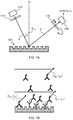
- the white circles represent an analyte
- the white Y-shaped structures represent a ligand (primary antibody)
- the black inverted Y-shaped structures represent a secondary antibody
- the white stars represent a fluorescent substance.
- a difference value between light component I p of fluorescence ⁇ having an angle of an oscillation direction of the electric field of 0° relative to the plane and light component I s of fluorescence ⁇ having an angle of an oscillation direction of the electric field of 90° relative to the plane can be obtained by subtracting equation 2 from equation 1.
- I p ⁇ I s ( I p1 ⁇ I s1 )+( I p2 ⁇ I s2 )+( I p3 ⁇ I s3 ) (Equation 3)
- a fluorescent substance excited by enhanced electric fields scarcely emit light with an angle of an oscillation direction of the electric field of 90° relative to the plane and light close to light with an angle of an oscillation direction of the electric field of 90° relative to the plane.
- light components (I s1 ) and (I s3 ), of fluorescence ⁇ emitted from a fluorescent substance present in a region where enhanced electric fields are exerted, having an angle of an oscillation direction of the electric field of 90° relative to the plane can be approximated to zero. Accordingly, the aforementioned equation 3 becomes equation 4.
- I p ⁇ I s I p1 +( I p2 ⁇ I s2 )+ I p3 (Equation 4)
- the second term of “I p2 ⁇ I s2 ” in the right-hand side is a difference value between a light component, of fluorescence ⁇ emitted from a suspended fluorescent substance positioned in space where enhanced electric fields are not exerted, having an angle of an oscillation direction of the electric field of 0° relative to the plane, and a light component, of fluorescence ⁇ emitted from a suspended fluorescent substance positioned in space where enhanced electric fields are not exerted, having an angle of an oscillation direction of the electric field of 90° relative to the plane.
- the aforementioned equation 4 becomes equation 5.
- I p ⁇ I s I p1 +I p3 (Equation 5)
- a light component (I p3 ), of fluorescence ⁇ emitted from a fluorescent substance nonspecifically adhered to metal film 220 , having an angle of an oscillation direction of the electric field of 0° relative to the plane is an extremely small value compared with a light component (I p1 ), of fluorescence ⁇ emitted from a fluorescent substance that labels an analyte, having an angle of the oscillation direction of the electric field of 0° relative to the plane, and thus is approximated to zero.
- the aforementioned equation 5 becomes equation 6.
- I p ⁇ I s I p1 (Equation 6)
- SPFS apparatus 100 of the embodiment can detect an analyte with higher sensitivity than conventional SPFS apparatuses, since only a signal component can be detected utilizing the difference in polarization characteristics between a signal component and a noise component.
- SPFS apparatus 100 of the embodiment can remove a noise component contained in fluorescence ⁇ , an analyte can be detected without removal of a free secondary antibody (washing of metal film 220 ; step S 80 ) after performing the primary reaction and the secondary reaction (step S 70 ).
- diffraction grating 230 (chip 200 ) is rotated around normal line N to metal film 220 as a rotational axis
- the optical axis of excitation light ⁇ may be rotated relative to diffraction grating 230 (chip 200 ).
- chip 200 may be irradiated with excitation light ⁇ from the side of substrate 210 .
- SPFS apparatus 300 according to Embodiment 2 is different from SPFS apparatus 100 according to Embodiment 1 in that the configuration of rotation section 320 differs from that of rotation section 120 .
- the configuration of rotation section 320 will be primarily described.
- the same components as those of SPFS apparatus 100 are denoted by the same numerals, and thus their descriptions will be omitted.
- Chip 200 is the same as chip 200 according to Embodiment 1, and thus the description will be omitted.
- FIG. 8 is a schematic view illustrating a configuration of SPFS apparatus 300 according to Embodiment 2.
- SPFS apparatus 300 according to Embodiment 2 includes excitation light irradiation unit 110 , rotation section 320 , fluorescence detection unit 130 , and control section 140 .
- Rotation section 320 changes the polarization direction of excitation light ⁇ relative to diffraction grating 230 .
- Rotation section 320 is connected to first polarizer 114 , and rotates first polarizer 114 around the optical axis of excitation light ⁇ as a central axis. By rotating first polarizer 114 , the polarization direction of linearly polarized excitation light ⁇ is rotated.
- FIG. 9 is a flow chart showing an example of an operational procedure of SPFS apparatus 300 .
- the same steps as those in the detection operations of SPFS apparatus 100 according to Embodiment 1 are denoted by the same numerals, and thus their detailed descriptions will be omitted.
- the measurement is prepared (step S 10 ).
- incident angle ⁇ 1 ( ⁇ 1a , ⁇ 1b ) of excitation light ⁇ is determined (step S 220 ).
- control section 140 irradiates a predetermined position of metal film 220 with excitation light ⁇ while a first angle adjustment section scans over incident angle ⁇ 1a of excitation light ⁇ relative to normal line N to a surface of metal film 220 in a side view of chip 200 .
- Control section 140 also controls a second angle adjustment section so that light detection section 134 detects reflected light ⁇ from above metal film 220 . Reflected light ⁇ reflected on metal film 220 reaches light detection section 134 .
- control section 140 obtains data containing a relationship between incident angle ⁇ 1a of excitation light ⁇ in a side view of chip 200 and light quantity of reflected light ⁇ . After that, control section 140 analyzes the data and determines incident angle ⁇ 1a at which light quantity of reflected light ⁇ (of excitation light ⁇ ) becomes minimum. When incident angle ⁇ 1a of excitation light ⁇ is measured, incident angle ⁇ 1b of excitation light ⁇ is set to 0°. Control section 140 determines incident angle ⁇ 1 ( ⁇ 1a , ⁇ 1b ) of excitation light ⁇ composed of ⁇ 1b and incident angle ⁇ 1a at which light quantity of reflected light ⁇ (of excitation light ⁇ ) becomes minimum.
- control section 140 irradiates a predetermined position of metal film 220 with excitation light ⁇ after providing a fluorescent labeling solution containing a secondary antibody labeled with a fluorescent substance, and simultaneously drives rotation section 320 to rotate (scan) first polarizer 114 around the optical axis of excitation light ⁇ as a central axis.
- incident angle ⁇ 1 ( ⁇ 1a , ⁇ 1b ) is the angle obtained in step S 220 .
- Control section 140 also adjusts a rotation angle of second polarizer 132 so that only the first light contained in fluorescence ⁇ is transmitted through.
- Light detection section 134 outputs a measured result (output O 1 ) to control section (processing section) 140 .
- Output O 1 is the fluorescence intensity of the first light (e.g., light with an angle of an oscillation direction of the electric field of 0° relative to the plane), of fluorescence ⁇ emitted from a suspended fluorescent substance above metal film 220 (noise component).
- step S 240 the fluorescence intensity of a second light is measured (step S 240 ). Specifically, in the same manner as in step S 230 , control section 140 irradiates a predetermined position of metal film 220 with excitation light ⁇ and simultaneously drives rotation section 320 to rotate (scan) first polarizer 114 around the optical axis of excitation light ⁇ as a central axis. In this step, incident angle ⁇ 1 ( ⁇ 1a , ⁇ 1b ) is the angle obtained in step S 220 . Control section 140 also adjusts a rotation angle of second polarizer 132 so that only the second light contained in fluorescence ⁇ is transmitted through.
- Light detection section 134 outputs a measured result (output O 2 ) to control section (processing section) 140 .
- Output O 2 is the fluorescence intensity of the second light (e.g., light with an angle of the oscillation direction of the electric field of 90° relative to the plane), of fluorescence ⁇ emitted from a suspended fluorescent substance above metal film 220 (noise component).
- control section 140 determines the polarization direction of excitation light ⁇ (step S 250 ). Specifically, control section 140 obtains, from the measured results (output O 1 and output O 2 ) obtained in step S 230 and step S 240 , the polarization direction of excitation light ⁇ when a difference value between the fluorescence intensity of the first light and the fluorescence intensity of the second light becomes zero. Thus, control section 140 determines the polarization direction of excitation light ⁇ as the direction in which a difference value between the fluorescence intensity of the first light and the fluorescence intensity of the second light becomes zero.
- Control section 140 then adjusts the polarization direction of linearly polarized excitation light ⁇ (step S 260 ). Specifically, control section 140 rotates first polarizer 114 so that the polarization direction of first polarizer 114 becomes the direction obtained in step S 250 .
- control section 140 reacts an analyte in a sample with a primary antibody while reacting the analyte with a labeled secondary antibody (primary reaction, secondary reaction: step S 70 ).
- metal film 220 is washed (step S 80 ).
- control section 140 operates light source 112 to emit excitation light ⁇ .
- control section 140 operates light detection section 134 to detect the intensity of fluorescence ⁇ from metal film 220 .
- control section 140 adjusts a rotation angle of second polarizer 132 so that only the third light contained in fluorescence ⁇ (in the figure, light with an angle of an oscillation direction of the electric field of 0° relative to the plane) is transmitted through.
- incident angle ⁇ 1 ( ⁇ 1a , ⁇ 1b ) is the angle obtained in step S 220
- the polarization direction of first polarizer is the direction obtained in step S 260 .
- Light detection section 134 outputs a measured result (output Op) to control section (processing section) 140 .
- Output Op contains a signal component and at least part of the fluorescent intensity of the first light.
- control section 140 operates light source 112 to emit excitation light ⁇ .
- control section 140 operates light detection section 134 to detect the intensity of fluorescence ⁇ from metal film 220 .
- control section 140 adjusts a rotation angle of second polarizer 132 so that only the fourth light contained in fluorescence ⁇ (in the figure, light with an angle of the oscillation direction of the electric field of 90° relative to the plane) is transmitted through.
- incident angle ⁇ 1 ( ⁇ 1a , ⁇ 1b ) is the angle obtained in step S 220
- the polarization direction of first polarizer 114 is the direction obtained in step S 260 .
- Light detection section 134 outputs a measured result (output Os) to control section (processing section) 140 .
- Output Os is primarily at least part of the fluorescence intensity of the second light.
- control section (processing section) 140 analyzes the output signals (outputs Op and Os) from light detection section 134 , and analyzes the presence of an analyte or an amount of an analyte (step S 310 ). Specifically, control section (processing section) 140 calculates a difference value between output Op and output Os to obtain a signal value.
- the surface plasmon-field enhanced fluorescence measurement method according to Embodiment 2 can also accurately detect the fluorescence intensity of fluorescence ⁇ emitted from a fluorescent substance that labels an analyte even when the fluorescence intensity of the first light (of fluorescence ⁇ from a suspended fluorescent substance) and the fluorescence intensity of the second light (of fluorescence ⁇ from a suspended fluorescent substance) are different values.
- SPFS apparatus 300 of the embodiment exerts the same advantageous effects as those exerted by SPFS apparatus 100 of Embodiment 1.
- SPFS apparatus 400 illustrated in FIG. 10 may be used. As illustrated in FIG. 10 , SPFS apparatus 400 is configured in the same manner as SPFS apparatuses 100 and 300 except that half-mirror 431 , third polarizer 432 , and light detection section 434 are further included.
- Half-mirror 431 is disposed on the optical path of fluorescence ⁇ between diffraction grating 230 and second polarizer 132 .
- Light detection section 434 is disposed on the optical path of fluorescence ⁇ reflected on half-mirror 431 (reflected light path), and third polarizer 432 is disposed on reflected light ⁇ path between half-mirror 431 and light detection section 434 .
- An rotation angle of second polarizer 132 is adjusted so that a first light and a third light (e.g., light with an angle of an oscillation of the electric field of 0° relative to the plane) are transmitted through, and an rotation angle of the third polarizer 432 is adjusted (or fixed) so that a second light and a fourth light (e.g., light with an angle of an oscillation of the electric field of 90° relative to the plane) are transmitted through.
- a polarizing beam splitter may be used in place of half-mirror 431 , second polarizer 132 , and third polarizer 432 .
- SPFS apparatus 400 can simultaneously measure the first light and the second light, as well as the third light and the fourth light since half-mirror 431 , third polarizer 432 , and light detection section 434 are further included.
- incident angle ⁇ 1b is 10° in a plan view of chip 200 .
- a liquid containing only a fluorescent substance was provided to on metal film 220 without providing a sample containing an analyte.
- incident angle ⁇ 1a of excitation light ⁇ in a side view of chip 200 was set to an angle at which light quantity of reflected light ⁇ (of excitation light ⁇ ) becomes minimum, and the polarization direction (angle) of excitation light ⁇ relative to a plane (containing normal line N to a surface of metal film 220 and the optical axis of excitation light ⁇ ) was set to 0°.
- diffraction grating 230 was irradiated with excitation light ⁇ having a predetermined wavelength.
- the number of photons was measured for light, of fluorescence emitted from a suspended fluorescent substance, having an angle of an oscillation direction of the electric field of 0° relative to the plane, and for light, of the fluorescence emitted from a suspended fluorescent substance, having an angle of an oscillation direction of the electric field of 90° relative to the plane while a light receiving angle at light detection section 134 was changed.
- FIG. 11A is a schematic view illustrating a procedure of the reference experiment.
- FIG. 12A is a graph showing a relationship between a light receiving angle at light detection section 134 and the number of photons for fluorescence ⁇ emitted from a suspended fluorescent substance.
- the horizontal axis is a light receiving angle ⁇ 3 (°) at light detection section 134
- the vertical axis is the number of photons (count) for fluorescence.
- the solid line represents light with an angle of an oscillation direction of the electric field of 0° relative to the plane (at incident angle ⁇ 1b of) 10°
- the broken line represents light with an angle of an oscillation direction of the electric field of 90° relative to the plane.
- the number of photons for light with an angle of an oscillation direction of the electric field of 0° relative to the plane temporarily lowered near the light receiving angle of 15°.
- incident angle ⁇ 1b is 10° in a plan view of chip 200
- the light receiving angles at which the number of photons for light with an angle of an oscillation direction of the electric field of 0° relative to the plane temporarily lowered are the optimal light receiving angles for the detection of fluorescence ⁇ .
- the temporal lowering in the number of photons for light with an angle of an oscillation direction of the electric field of 0° relative to the plane is presumably due to temporal lowering in the intensity of enhanced electric fields at the light receiving angles.
- FIG. 11B is a schematic view illustrating a procedure of the reference experiment.
- FIG. 12B is a graph showing a relationship between a light receiving angle at light detection section 134 and the number of photons for fluorescence ⁇ .
- the horizontal axis is a light receiving angle ⁇ 3 (°) at light detection section 134
- the vertical axis is the number of photons (count) for fluorescence.
- the solid line represents light with an angle of an oscillation direction of the electric field of 0° relative to the plane
- the broken line represents light with an angle of an oscillation direction of the electric field of 90° relative to the plane.
- incident angle ⁇ 1a was set to 10°
- incident angle ⁇ 1b was set to 0°
- diffraction grating 230 was irradiated with excitation light ⁇ having a predetermined wavelength.
- the number of photons was measured for light, emitted from a suspended or an immobilized fluorescent substance, having an angle of an oscillation direction of the electric field of 0° relative to the plane, and for light having an angle of an oscillation direction of the electric field of 90° relative to the plane while the polarization direction of excitation light ⁇ was changed.
- FIG. 13A is a graph showing a relationship between the polarization direction and the number of photons for fluorescence emitted from a fluorescent substance.
- the horizontal axis represents the polarization direction (°) of excitation light ⁇
- the vertical axis represents the number of photons (count) for fluorescence ⁇ .
- black circle symbols represent a fluorescence component light, of fluorescence ⁇ , having an angle of an oscillation direction of the electric field of 0° relative to the plane
- white circle symbols represent a fluorescence component light, of fluorescence ⁇ , having an angle of an oscillation direction of the electric field of 90° relative to the plane.
- the number of photons for light, of fluorescence ⁇ , having an angle of an oscillation direction of the electric field of 0° relative to the plane was maximum when excitation light ⁇ (light with an angle of an oscillation direction of the electric field of 0° relative to the plane) at incident angle ⁇ 1b of 0° at which light quantity of reflected light ⁇ (of excitation light ⁇ ) becomes minimum was irradiated.
- Difference values between the number of photons for light with an angle of an oscillation direction of the electric field of 0° relative to the plane and the number of photons for light with an angle of an oscillation direction of the electric field of 0° relative to the plane were zero near the polarization direction of ⁇ 50°.
- the number of photons for light, emitted from the fluorescent dye that labeled the analyte, having an angle of an oscillation direction of the electric field of 0° relative to the plane and the number of photons for light, emitted from the fluorescent dye that labeled the analyte, having an angle of an oscillation direction of the electric field of 90° relative to the plane were measured.
- FIG. 13B is a graph showing a relationship between the polarization direction and the number of photons for fluorescence ⁇ .
- the horizontal axis represents the polarization direction (°) of excitation light ⁇
- the vertical axis represents the number of photons (count) for fluorescence ⁇ .
- the black circle symbols represent light with an angle of an oscillation direction of the electric field of 0° relative to the plane
- the white circle symbols represent light with an angle of an oscillation direction of the electric field of 90° relative to the plane.
- fluorescence ⁇ emitted from a fluorescent substance could be measured even when the polarization direction of excitation light ⁇ was around ⁇ 50°.
- a signal component value with little noise component can be calculated by subtracting a detected result of a light component with an angle of an oscillation direction of the electric field of 90° relative to the plane from a detected result of a light component with an angle of an oscillation direction of the electric field of 0° relative to the plane, even when a noise component other than a signal component is contained in fluorescence ⁇ .
- the surface plasmon-field enhanced fluorescence measurement apparatus and the surface plasmon-field enhanced fluorescence measurement method according to the embodiment can measure an analyte highly reliably, and thus are useful for clinical tests, for example.
- the surface plasmon-field enhanced fluorescence measurement apparatus and the surface plasmon-field enhanced fluorescence measurement method according to the embodiment can also measure an analyte highly reliably without washing a metal film surface after a fluorescent labeling solution or the like is provided.
- the measurement apparatus and the measurement method according to the embodiment are expected to contribute to development, widespread use, and advancement of an extremely simple quantitative immunoassay system, as well as to the shortened measurement time.
Landscapes
- Health & Medical Sciences (AREA)
- Physics & Mathematics (AREA)
- Immunology (AREA)
- Life Sciences & Earth Sciences (AREA)
- General Physics & Mathematics (AREA)
- Spectroscopy & Molecular Physics (AREA)
- Chemical & Material Sciences (AREA)
- Engineering & Computer Science (AREA)
- Analytical Chemistry (AREA)
- Biochemistry (AREA)
- Pathology (AREA)
- General Health & Medical Sciences (AREA)
- Hematology (AREA)
- Biomedical Technology (AREA)
- Molecular Biology (AREA)
- Urology & Nephrology (AREA)
- Nuclear Medicine, Radiotherapy & Molecular Imaging (AREA)
- Microbiology (AREA)
- Medicinal Chemistry (AREA)
- Food Science & Technology (AREA)
- Cell Biology (AREA)
- Biotechnology (AREA)
- Chemical Kinetics & Catalysis (AREA)
- Optics & Photonics (AREA)
- Inorganic Chemistry (AREA)
- Investigating, Analyzing Materials By Fluorescence Or Luminescence (AREA)
Abstract
Description
-
PTL 1 - Japanese Patent Application Laid-Open No. 2011-158369
- NPL 1
- Keiko Tawa, Hironobu Hori, Kenji Kintaka, Kazuyuki Kiyosue, Yoshiro Tatsu, and Junji Nishii, “Optical microscopic observation of fluorescence enhanced by grating-coupled surface plasmon resonance,” Optics Express, Vol. 16, pp. 9781-9790
I p =I p1 +I p2 +I p3 (Equation 1)
I s =I s1 +I s2 +I s3 (Equation 2)
I p −I s=(I p1 −I s1)+(I p2 −I s2)+(I p3 −I s3) (Equation 3)
I p −I s =I p1+(I p2 −I s2)+I p3 (Equation 4)
I p −I s =I p1 +I p3 (Equation 5)
I p −I s =I p1 (Equation 6)
- 100, 300, 400 Surface plasmon-field enhanced fluorescence measurement apparatus (SPFS apparatus)
- 110 Excitation light irradiation unit
- 112 Light source
- 114 First polarizer
- 120, 320 Rotation section
- 122 Chip holder
- 124 Motor
- 130 Fluorescence detection unit
- 132 Second polarizer
- 134, 434 Light detection section
- 140 Control section (Processing section)
- 200 Chip
- 210 Substrate
- 220 Metal film
- 230 Diffraction grating
- 431 Half-mirror
- 432 Third polarizer
- α Excitation light
- β Fluorescence
- γ Reflected light
Claims (9)
Applications Claiming Priority (3)
| Application Number | Priority Date | Filing Date | Title |
|---|---|---|---|
| JP2014253193 | 2014-12-15 | ||
| JP2014-253193 | 2014-12-15 | ||
| PCT/JP2015/083763 WO2016098581A1 (en) | 2014-12-15 | 2015-12-01 | Surface plasmon-enhanced fluorescence measurement device and surface plasmon-enhanced fluorescence measurement method |
Publications (2)
| Publication Number | Publication Date |
|---|---|
| US20180017493A1 US20180017493A1 (en) | 2018-01-18 |
| US10690596B2 true US10690596B2 (en) | 2020-06-23 |
Family
ID=56126477
Family Applications (1)
| Application Number | Title | Priority Date | Filing Date |
|---|---|---|---|
| US15/536,109 Active 2037-01-29 US10690596B2 (en) | 2014-12-15 | 2015-12-01 | Surface plasmon-enhanced fluorescence measurement device and surface plasmon-enhanced fluorescence measurement method |
Country Status (4)
| Country | Link |
|---|---|
| US (1) | US10690596B2 (en) |
| EP (1) | EP3236242A4 (en) |
| JP (1) | JP6565934B2 (en) |
| WO (1) | WO2016098581A1 (en) |
Cited By (1)
| Publication number | Priority date | Publication date | Assignee | Title |
|---|---|---|---|---|
| US11946881B2 (en) | 2021-06-23 | 2024-04-02 | Samsung Electronics Co., Ltd. | Inspection apparatus and inspection method using same |
Families Citing this family (8)
| Publication number | Priority date | Publication date | Assignee | Title |
|---|---|---|---|---|
| US10845307B2 (en) | 2017-08-21 | 2020-11-24 | Saudi Arabian Oil Company | Determining composition of a sample |
| US10845306B2 (en) * | 2017-08-21 | 2020-11-24 | Saudi Arabian Oil Company | Determining composition of a sample |
| CN107515047B (en) * | 2017-09-20 | 2019-08-30 | 鲁东大学 | Device and method for detecting polarization orientation of sub-wavelength scale multi-focus spots |
| US20210318326A1 (en) * | 2018-08-06 | 2021-10-14 | Konica Minolta, Inc. | Method for measuring brain natriuretic peptide and kit for measuring brain natriuretic peptide |
| TWI687676B (en) * | 2019-04-29 | 2020-03-11 | 國立中正大學 | Biosensor self-compensation system |
| CN110261333B (en) * | 2019-06-04 | 2022-03-25 | 暨南大学 | Micro spectrum test system and test method |
| KR102116232B1 (en) * | 2019-11-12 | 2020-05-28 | (주)로고스바이오시스템스 | Sample detection device and sample detection method by using the same |
| US20240364984A1 (en) * | 2021-06-15 | 2024-10-31 | Sony Group Corporation | Imaging device and method of operating the same |
Citations (7)
| Publication number | Priority date | Publication date | Assignee | Title |
|---|---|---|---|---|
| JP2000515966A (en) | 1996-07-11 | 2000-11-28 | イーツェーベー インスティテュート ファー ヒェモ−ウント ビオゼンゾリック ミュンスター エー.ファー. | Apparatus and method for performing a quantitative fluorescent mark affinity test |
| US20050186565A1 (en) | 2003-02-10 | 2005-08-25 | American Environmental Systems, Inc. | Method and spectral/imaging device for optochemical sensing with plasmon-modified polarization |
| JP2008286778A (en) | 2007-04-16 | 2008-11-27 | National Institute Of Advanced Industrial & Technology | Microplate having periodic structure and surface plasmon excitation enhanced fluorescence microscope or fluorescence microplate reader using the same |
| US20090045351A1 (en) | 2007-01-22 | 2009-02-19 | University Of Maryland | Sensor system with surface-plasmon-polariton (spp) enhanced selective fluorescence excitation and method |
| JP2010038624A (en) | 2008-08-01 | 2010-02-18 | Fujifilm Corp | Detection method and detector |
| US7989220B2 (en) | 2008-04-22 | 2011-08-02 | University Of Maryland, Baltimore | Metal-enhanced fluorescence for polarization-based affinity assays |
| JP2011158369A (en) | 2010-02-02 | 2011-08-18 | National Institute Of Advanced Industrial Science & Technology | Biochip, kit for antigen-antibody reaction detection, and detection method for antigen-antibody reaction |
-
2015
- 2015-12-01 JP JP2016564769A patent/JP6565934B2/en active Active
- 2015-12-01 WO PCT/JP2015/083763 patent/WO2016098581A1/en not_active Ceased
- 2015-12-01 EP EP15869789.6A patent/EP3236242A4/en not_active Withdrawn
- 2015-12-01 US US15/536,109 patent/US10690596B2/en active Active
Patent Citations (8)
| Publication number | Priority date | Publication date | Assignee | Title |
|---|---|---|---|---|
| JP2000515966A (en) | 1996-07-11 | 2000-11-28 | イーツェーベー インスティテュート ファー ヒェモ−ウント ビオゼンゾリック ミュンスター エー.ファー. | Apparatus and method for performing a quantitative fluorescent mark affinity test |
| US6274872B1 (en) | 1996-07-11 | 2001-08-14 | Icb Institut Fuer Chemo- Und Biosensorik Menster E.V. | Process and device for carrying out quantitative, fluorescence affinity tests |
| US20050186565A1 (en) | 2003-02-10 | 2005-08-25 | American Environmental Systems, Inc. | Method and spectral/imaging device for optochemical sensing with plasmon-modified polarization |
| US20090045351A1 (en) | 2007-01-22 | 2009-02-19 | University Of Maryland | Sensor system with surface-plasmon-polariton (spp) enhanced selective fluorescence excitation and method |
| JP2008286778A (en) | 2007-04-16 | 2008-11-27 | National Institute Of Advanced Industrial & Technology | Microplate having periodic structure and surface plasmon excitation enhanced fluorescence microscope or fluorescence microplate reader using the same |
| US7989220B2 (en) | 2008-04-22 | 2011-08-02 | University Of Maryland, Baltimore | Metal-enhanced fluorescence for polarization-based affinity assays |
| JP2010038624A (en) | 2008-08-01 | 2010-02-18 | Fujifilm Corp | Detection method and detector |
| JP2011158369A (en) | 2010-02-02 | 2011-08-18 | National Institute Of Advanced Industrial Science & Technology | Biochip, kit for antigen-antibody reaction detection, and detection method for antigen-antibody reaction |
Non-Patent Citations (6)
| Title |
|---|
| Bauch et al.; "Plasmon-Enhanced Fluorescence Biosensors: a Review"; Plasmonics; vol. 9 No. 4; Dec. 2013; p. 781-799. |
| European Patent Application No. 15869789.6; Extended Search Report; dated Nov. 7, 2017; 8 pages. |
| International Patent Application No. PCT/JP2015/083763; Int'l Preliminary Report on Patentability; dated Jun. 29, 2017; 5 pages. |
| Japan Patent Application No. 2016-564769; Notice of Reasons for Refusal; dated May 28, 2019; 6 pages. |
| Keiko, Tawa et al.; "Optical microscopic observation of fluorescence enhanced by grating-coupled surface plasmon resonance"; Optics Express; vol. 16 No. 13; Jun. 2008; p. 9781-9790. |
| Tawa et al., "Optical microscopic observation of fluorescence enhanced by grating-coupled surface plasmon resonance", Optics Express, vol. 16, No. 13, pp. 9781-9790, Jun. 23, 2008. |
Cited By (1)
| Publication number | Priority date | Publication date | Assignee | Title |
|---|---|---|---|---|
| US11946881B2 (en) | 2021-06-23 | 2024-04-02 | Samsung Electronics Co., Ltd. | Inspection apparatus and inspection method using same |
Also Published As
| Publication number | Publication date |
|---|---|
| US20180017493A1 (en) | 2018-01-18 |
| WO2016098581A1 (en) | 2016-06-23 |
| JP6565934B2 (en) | 2019-08-28 |
| JPWO2016098581A1 (en) | 2017-09-28 |
| EP3236242A1 (en) | 2017-10-25 |
| EP3236242A4 (en) | 2017-12-06 |
Similar Documents
| Publication | Publication Date | Title |
|---|---|---|
| US10690596B2 (en) | Surface plasmon-enhanced fluorescence measurement device and surface plasmon-enhanced fluorescence measurement method | |
| EP3495802B1 (en) | Detection chip, detection system, and detection method | |
| US20200256796A1 (en) | Method of manufacturing sensing chip and sensing chip | |
| EP3321688B1 (en) | Detection device and detection method | |
| EP3315970B1 (en) | Measurement method, measurement chip used for same, and kit for measurement | |
| JP6760384B2 (en) | Measuring method | |
| JP6263887B2 (en) | Surface plasmon enhanced fluorescence measurement method and surface plasmon enhanced fluorescence measurement apparatus | |
| US10254228B2 (en) | Detection chip and detection method | |
| WO2017057136A1 (en) | Surface plasmon-field enhanced fluorescence spectroscopy and measurement kit | |
| JP2015111063A (en) | Surface plasmon-field enhanced fluorescence measurement method and surface plasmon enhanced fluorescence measurement apparatus | |
| JP6263884B2 (en) | Surface plasmon enhanced fluorescence measuring apparatus and surface plasmon enhanced fluorescence measuring method | |
| US10495575B2 (en) | Surface plasmon enhanced fluorescence measurement device and surface plasmon enhanced fluorescence measurement method | |
| JP6627778B2 (en) | Detection device and detection method | |
| JP6586884B2 (en) | Chip and surface plasmon enhanced fluorescence measurement method | |
| JP6717201B2 (en) | Detection method and detection device | |
| JP2012233860A (en) | Assay method of object to be analyzed in biological specimen and poct apparatus used therefor | |
| JP6711285B2 (en) | Detection method, detection device and chip | |
| US20230184676A1 (en) | Detection device and detection method |
Legal Events
| Date | Code | Title | Description |
|---|---|---|---|
| AS | Assignment |
Owner name: KONICA MINOLTA, INC., JAPAN Free format text: ASSIGNMENT OF ASSIGNORS INTEREST;ASSIGNORS:NAKAMURA, YUKITO;NAGAE, KOSUKE;KAYA, TAKATOSHI;REEL/FRAME:042727/0439 Effective date: 20170522 |
|
| STPP | Information on status: patent application and granting procedure in general |
Free format text: DOCKETED NEW CASE - READY FOR EXAMINATION |
|
| STPP | Information on status: patent application and granting procedure in general |
Free format text: NON FINAL ACTION MAILED |
|
| STPP | Information on status: patent application and granting procedure in general |
Free format text: RESPONSE TO NON-FINAL OFFICE ACTION ENTERED AND FORWARDED TO EXAMINER |
|
| STPP | Information on status: patent application and granting procedure in general |
Free format text: NOTICE OF ALLOWANCE MAILED -- APPLICATION RECEIVED IN OFFICE OF PUBLICATIONS |
|
| STPP | Information on status: patent application and granting procedure in general |
Free format text: PUBLICATIONS -- ISSUE FEE PAYMENT VERIFIED |
|
| STCF | Information on status: patent grant |
Free format text: PATENTED CASE |
|
| AS | Assignment |
Owner name: OTSUKA PHARMACEUTICAL CO., LTD., JAPAN Free format text: ASSIGNMENT OF ASSIGNORS INTEREST;ASSIGNOR:KONICA MINOLTA, INC.;REEL/FRAME:059747/0589 Effective date: 20220414 |
|
| MAFP | Maintenance fee payment |
Free format text: PAYMENT OF MAINTENANCE FEE, 4TH YEAR, LARGE ENTITY (ORIGINAL EVENT CODE: M1551); ENTITY STATUS OF PATENT OWNER: LARGE ENTITY Year of fee payment: 4 |