US10685948B1 - Double side mounted large MCM package with memory channel length reduction - Google Patents
Double side mounted large MCM package with memory channel length reduction Download PDFInfo
- Publication number
- US10685948B1 US10685948B1 US16/204,679 US201816204679A US10685948B1 US 10685948 B1 US10685948 B1 US 10685948B1 US 201816204679 A US201816204679 A US 201816204679A US 10685948 B1 US10685948 B1 US 10685948B1
- Authority
- US
- United States
- Prior art keywords
- substrate
- routing
- module substrate
- bottom side
- memory packages
- Prior art date
- Legal status (The legal status is an assumption and is not a legal conclusion. Google has not performed a legal analysis and makes no representation as to the accuracy of the status listed.)
- Active
Links
- 239000000758 substrate Substances 0.000 claims abstract description 193
- 229910000679 solder Inorganic materials 0.000 claims description 24
- 239000003351 stiffener Substances 0.000 claims description 17
- 238000000034 method Methods 0.000 description 6
- 230000010354 integration Effects 0.000 description 2
- 239000000463 material Substances 0.000 description 2
- 238000004806 packaging method and process Methods 0.000 description 2
- 239000000853 adhesive Substances 0.000 description 1
- 230000001070 adhesive effect Effects 0.000 description 1
- 238000003491 array Methods 0.000 description 1
- 230000015572 biosynthetic process Effects 0.000 description 1
- 239000003990 capacitor Substances 0.000 description 1
- 230000015556 catabolic process Effects 0.000 description 1
- 238000006731 degradation reaction Methods 0.000 description 1
- 230000000694 effects Effects 0.000 description 1
- 238000005516 engineering process Methods 0.000 description 1
- 230000006870 function Effects 0.000 description 1
- 238000004519 manufacturing process Methods 0.000 description 1
- 239000012778 molding material Substances 0.000 description 1
- 238000000059 patterning Methods 0.000 description 1
- 239000004065 semiconductor Substances 0.000 description 1
Images


Classifications
-
- H—ELECTRICITY
- H01—ELECTRIC ELEMENTS
- H01L—SEMICONDUCTOR DEVICES NOT COVERED BY CLASS H10
- H01L25/00—Assemblies consisting of a plurality of individual semiconductor or other solid state devices ; Multistep manufacturing processes thereof
- H01L25/03—Assemblies consisting of a plurality of individual semiconductor or other solid state devices ; Multistep manufacturing processes thereof all the devices being of a type provided for in the same subgroup of groups H01L27/00 - H01L33/00, or in a single subclass of H10K, H10N, e.g. assemblies of rectifier diodes
- H01L25/10—Assemblies consisting of a plurality of individual semiconductor or other solid state devices ; Multistep manufacturing processes thereof all the devices being of a type provided for in the same subgroup of groups H01L27/00 - H01L33/00, or in a single subclass of H10K, H10N, e.g. assemblies of rectifier diodes the devices having separate containers
- H01L25/105—Assemblies consisting of a plurality of individual semiconductor or other solid state devices ; Multistep manufacturing processes thereof all the devices being of a type provided for in the same subgroup of groups H01L27/00 - H01L33/00, or in a single subclass of H10K, H10N, e.g. assemblies of rectifier diodes the devices having separate containers the devices being of a type provided for in group H01L27/00
-
- H—ELECTRICITY
- H01—ELECTRIC ELEMENTS
- H01L—SEMICONDUCTOR DEVICES NOT COVERED BY CLASS H10
- H01L25/00—Assemblies consisting of a plurality of individual semiconductor or other solid state devices ; Multistep manufacturing processes thereof
- H01L25/18—Assemblies consisting of a plurality of individual semiconductor or other solid state devices ; Multistep manufacturing processes thereof the devices being of types provided for in two or more different subgroups of the same main group of groups H01L27/00 - H01L33/00, or in a single subclass of H10K, H10N
-
- H—ELECTRICITY
- H01—ELECTRIC ELEMENTS
- H01L—SEMICONDUCTOR DEVICES NOT COVERED BY CLASS H10
- H01L23/00—Details of semiconductor or other solid state devices
- H01L23/16—Fillings or auxiliary members in containers or encapsulations, e.g. centering rings
-
- H—ELECTRICITY
- H01—ELECTRIC ELEMENTS
- H01L—SEMICONDUCTOR DEVICES NOT COVERED BY CLASS H10
- H01L23/00—Details of semiconductor or other solid state devices
- H01L23/52—Arrangements for conducting electric current within the device in operation from one component to another, i.e. interconnections, e.g. wires, lead frames
- H01L23/538—Arrangements for conducting electric current within the device in operation from one component to another, i.e. interconnections, e.g. wires, lead frames the interconnection structure between a plurality of semiconductor chips being formed on, or in, insulating substrates
- H01L23/5385—Assembly of a plurality of insulating substrates
-
- H—ELECTRICITY
- H01—ELECTRIC ELEMENTS
- H01L—SEMICONDUCTOR DEVICES NOT COVERED BY CLASS H10
- H01L23/00—Details of semiconductor or other solid state devices
- H01L23/562—Protection against mechanical damage
-
- H—ELECTRICITY
- H01—ELECTRIC ELEMENTS
- H01L—SEMICONDUCTOR DEVICES NOT COVERED BY CLASS H10
- H01L2224/00—Indexing scheme for arrangements for connecting or disconnecting semiconductor or solid-state bodies and methods related thereto as covered by H01L24/00
- H01L2224/01—Means for bonding being attached to, or being formed on, the surface to be connected, e.g. chip-to-package, die-attach, "first-level" interconnects; Manufacturing methods related thereto
- H01L2224/02—Bonding areas; Manufacturing methods related thereto
- H01L2224/04—Structure, shape, material or disposition of the bonding areas prior to the connecting process
- H01L2224/0401—Bonding areas specifically adapted for bump connectors, e.g. under bump metallisation [UBM]
-
- H—ELECTRICITY
- H01—ELECTRIC ELEMENTS
- H01L—SEMICONDUCTOR DEVICES NOT COVERED BY CLASS H10
- H01L2224/00—Indexing scheme for arrangements for connecting or disconnecting semiconductor or solid-state bodies and methods related thereto as covered by H01L24/00
- H01L2224/01—Means for bonding being attached to, or being formed on, the surface to be connected, e.g. chip-to-package, die-attach, "first-level" interconnects; Manufacturing methods related thereto
- H01L2224/10—Bump connectors; Manufacturing methods related thereto
- H01L2224/12—Structure, shape, material or disposition of the bump connectors prior to the connecting process
- H01L2224/13—Structure, shape, material or disposition of the bump connectors prior to the connecting process of an individual bump connector
- H01L2224/13001—Core members of the bump connector
- H01L2224/13099—Material
- H01L2224/131—Material with a principal constituent of the material being a metal or a metalloid, e.g. boron [B], silicon [Si], germanium [Ge], arsenic [As], antimony [Sb], tellurium [Te] and polonium [Po], and alloys thereof
-
- H—ELECTRICITY
- H01—ELECTRIC ELEMENTS
- H01L—SEMICONDUCTOR DEVICES NOT COVERED BY CLASS H10
- H01L2224/00—Indexing scheme for arrangements for connecting or disconnecting semiconductor or solid-state bodies and methods related thereto as covered by H01L24/00
- H01L2224/01—Means for bonding being attached to, or being formed on, the surface to be connected, e.g. chip-to-package, die-attach, "first-level" interconnects; Manufacturing methods related thereto
- H01L2224/10—Bump connectors; Manufacturing methods related thereto
- H01L2224/15—Structure, shape, material or disposition of the bump connectors after the connecting process
- H01L2224/16—Structure, shape, material or disposition of the bump connectors after the connecting process of an individual bump connector
- H01L2224/161—Disposition
- H01L2224/16151—Disposition the bump connector connecting between a semiconductor or solid-state body and an item not being a semiconductor or solid-state body, e.g. chip-to-substrate, chip-to-passive
- H01L2224/16221—Disposition the bump connector connecting between a semiconductor or solid-state body and an item not being a semiconductor or solid-state body, e.g. chip-to-substrate, chip-to-passive the body and the item being stacked
- H01L2224/16225—Disposition the bump connector connecting between a semiconductor or solid-state body and an item not being a semiconductor or solid-state body, e.g. chip-to-substrate, chip-to-passive the body and the item being stacked the item being non-metallic, e.g. insulating substrate with or without metallisation
- H01L2224/16227—Disposition the bump connector connecting between a semiconductor or solid-state body and an item not being a semiconductor or solid-state body, e.g. chip-to-substrate, chip-to-passive the body and the item being stacked the item being non-metallic, e.g. insulating substrate with or without metallisation the bump connector connecting to a bond pad of the item
-
- H—ELECTRICITY
- H01—ELECTRIC ELEMENTS
- H01L—SEMICONDUCTOR DEVICES NOT COVERED BY CLASS H10
- H01L2224/00—Indexing scheme for arrangements for connecting or disconnecting semiconductor or solid-state bodies and methods related thereto as covered by H01L24/00
- H01L2224/01—Means for bonding being attached to, or being formed on, the surface to be connected, e.g. chip-to-package, die-attach, "first-level" interconnects; Manufacturing methods related thereto
- H01L2224/10—Bump connectors; Manufacturing methods related thereto
- H01L2224/15—Structure, shape, material or disposition of the bump connectors after the connecting process
- H01L2224/16—Structure, shape, material or disposition of the bump connectors after the connecting process of an individual bump connector
- H01L2224/161—Disposition
- H01L2224/16151—Disposition the bump connector connecting between a semiconductor or solid-state body and an item not being a semiconductor or solid-state body, e.g. chip-to-substrate, chip-to-passive
- H01L2224/16221—Disposition the bump connector connecting between a semiconductor or solid-state body and an item not being a semiconductor or solid-state body, e.g. chip-to-substrate, chip-to-passive the body and the item being stacked
- H01L2224/16225—Disposition the bump connector connecting between a semiconductor or solid-state body and an item not being a semiconductor or solid-state body, e.g. chip-to-substrate, chip-to-passive the body and the item being stacked the item being non-metallic, e.g. insulating substrate with or without metallisation
- H01L2224/16235—Disposition the bump connector connecting between a semiconductor or solid-state body and an item not being a semiconductor or solid-state body, e.g. chip-to-substrate, chip-to-passive the body and the item being stacked the item being non-metallic, e.g. insulating substrate with or without metallisation the bump connector connecting to a via metallisation of the item
-
- H—ELECTRICITY
- H01—ELECTRIC ELEMENTS
- H01L—SEMICONDUCTOR DEVICES NOT COVERED BY CLASS H10
- H01L2224/00—Indexing scheme for arrangements for connecting or disconnecting semiconductor or solid-state bodies and methods related thereto as covered by H01L24/00
- H01L2224/01—Means for bonding being attached to, or being formed on, the surface to be connected, e.g. chip-to-package, die-attach, "first-level" interconnects; Manufacturing methods related thereto
- H01L2224/26—Layer connectors, e.g. plate connectors, solder or adhesive layers; Manufacturing methods related thereto
- H01L2224/31—Structure, shape, material or disposition of the layer connectors after the connecting process
- H01L2224/32—Structure, shape, material or disposition of the layer connectors after the connecting process of an individual layer connector
- H01L2224/321—Disposition
- H01L2224/32135—Disposition the layer connector connecting between different semiconductor or solid-state bodies, i.e. chip-to-chip
- H01L2224/32145—Disposition the layer connector connecting between different semiconductor or solid-state bodies, i.e. chip-to-chip the bodies being stacked
-
- H—ELECTRICITY
- H01—ELECTRIC ELEMENTS
- H01L—SEMICONDUCTOR DEVICES NOT COVERED BY CLASS H10
- H01L2224/00—Indexing scheme for arrangements for connecting or disconnecting semiconductor or solid-state bodies and methods related thereto as covered by H01L24/00
- H01L2224/01—Means for bonding being attached to, or being formed on, the surface to be connected, e.g. chip-to-package, die-attach, "first-level" interconnects; Manufacturing methods related thereto
- H01L2224/26—Layer connectors, e.g. plate connectors, solder or adhesive layers; Manufacturing methods related thereto
- H01L2224/31—Structure, shape, material or disposition of the layer connectors after the connecting process
- H01L2224/32—Structure, shape, material or disposition of the layer connectors after the connecting process of an individual layer connector
- H01L2224/321—Disposition
- H01L2224/32151—Disposition the layer connector connecting between a semiconductor or solid-state body and an item not being a semiconductor or solid-state body, e.g. chip-to-substrate, chip-to-passive
- H01L2224/32221—Disposition the layer connector connecting between a semiconductor or solid-state body and an item not being a semiconductor or solid-state body, e.g. chip-to-substrate, chip-to-passive the body and the item being stacked
- H01L2224/32225—Disposition the layer connector connecting between a semiconductor or solid-state body and an item not being a semiconductor or solid-state body, e.g. chip-to-substrate, chip-to-passive the body and the item being stacked the item being non-metallic, e.g. insulating substrate with or without metallisation
-
- H—ELECTRICITY
- H01—ELECTRIC ELEMENTS
- H01L—SEMICONDUCTOR DEVICES NOT COVERED BY CLASS H10
- H01L2224/00—Indexing scheme for arrangements for connecting or disconnecting semiconductor or solid-state bodies and methods related thereto as covered by H01L24/00
- H01L2224/01—Means for bonding being attached to, or being formed on, the surface to be connected, e.g. chip-to-package, die-attach, "first-level" interconnects; Manufacturing methods related thereto
- H01L2224/42—Wire connectors; Manufacturing methods related thereto
- H01L2224/47—Structure, shape, material or disposition of the wire connectors after the connecting process
- H01L2224/48—Structure, shape, material or disposition of the wire connectors after the connecting process of an individual wire connector
- H01L2224/4805—Shape
- H01L2224/4809—Loop shape
- H01L2224/48091—Arched
-
- H—ELECTRICITY
- H01—ELECTRIC ELEMENTS
- H01L—SEMICONDUCTOR DEVICES NOT COVERED BY CLASS H10
- H01L2224/00—Indexing scheme for arrangements for connecting or disconnecting semiconductor or solid-state bodies and methods related thereto as covered by H01L24/00
- H01L2224/01—Means for bonding being attached to, or being formed on, the surface to be connected, e.g. chip-to-package, die-attach, "first-level" interconnects; Manufacturing methods related thereto
- H01L2224/42—Wire connectors; Manufacturing methods related thereto
- H01L2224/47—Structure, shape, material or disposition of the wire connectors after the connecting process
- H01L2224/48—Structure, shape, material or disposition of the wire connectors after the connecting process of an individual wire connector
- H01L2224/481—Disposition
- H01L2224/48151—Connecting between a semiconductor or solid-state body and an item not being a semiconductor or solid-state body, e.g. chip-to-substrate, chip-to-passive
- H01L2224/48221—Connecting between a semiconductor or solid-state body and an item not being a semiconductor or solid-state body, e.g. chip-to-substrate, chip-to-passive the body and the item being stacked
- H01L2224/48225—Connecting between a semiconductor or solid-state body and an item not being a semiconductor or solid-state body, e.g. chip-to-substrate, chip-to-passive the body and the item being stacked the item being non-metallic, e.g. insulating substrate with or without metallisation
- H01L2224/48227—Connecting between a semiconductor or solid-state body and an item not being a semiconductor or solid-state body, e.g. chip-to-substrate, chip-to-passive the body and the item being stacked the item being non-metallic, e.g. insulating substrate with or without metallisation connecting the wire to a bond pad of the item
-
- H—ELECTRICITY
- H01—ELECTRIC ELEMENTS
- H01L—SEMICONDUCTOR DEVICES NOT COVERED BY CLASS H10
- H01L2224/00—Indexing scheme for arrangements for connecting or disconnecting semiconductor or solid-state bodies and methods related thereto as covered by H01L24/00
- H01L2224/73—Means for bonding being of different types provided for in two or more of groups H01L2224/10, H01L2224/18, H01L2224/26, H01L2224/34, H01L2224/42, H01L2224/50, H01L2224/63, H01L2224/71
- H01L2224/732—Location after the connecting process
- H01L2224/73201—Location after the connecting process on the same surface
- H01L2224/73203—Bump and layer connectors
- H01L2224/73204—Bump and layer connectors the bump connector being embedded into the layer connector
-
- H—ELECTRICITY
- H01—ELECTRIC ELEMENTS
- H01L—SEMICONDUCTOR DEVICES NOT COVERED BY CLASS H10
- H01L2224/00—Indexing scheme for arrangements for connecting or disconnecting semiconductor or solid-state bodies and methods related thereto as covered by H01L24/00
- H01L2224/73—Means for bonding being of different types provided for in two or more of groups H01L2224/10, H01L2224/18, H01L2224/26, H01L2224/34, H01L2224/42, H01L2224/50, H01L2224/63, H01L2224/71
- H01L2224/732—Location after the connecting process
- H01L2224/73251—Location after the connecting process on different surfaces
- H01L2224/73265—Layer and wire connectors
-
- H—ELECTRICITY
- H01—ELECTRIC ELEMENTS
- H01L—SEMICONDUCTOR DEVICES NOT COVERED BY CLASS H10
- H01L2224/00—Indexing scheme for arrangements for connecting or disconnecting semiconductor or solid-state bodies and methods related thereto as covered by H01L24/00
- H01L2224/91—Methods for connecting semiconductor or solid state bodies including different methods provided for in two or more of groups H01L2224/80 - H01L2224/90
- H01L2224/92—Specific sequence of method steps
- H01L2224/921—Connecting a surface with connectors of different types
- H01L2224/9212—Sequential connecting processes
- H01L2224/92122—Sequential connecting processes the first connecting process involving a bump connector
- H01L2224/92125—Sequential connecting processes the first connecting process involving a bump connector the second connecting process involving a layer connector
-
- H—ELECTRICITY
- H01—ELECTRIC ELEMENTS
- H01L—SEMICONDUCTOR DEVICES NOT COVERED BY CLASS H10
- H01L2225/00—Details relating to assemblies covered by the group H01L25/00 but not provided for in its subgroups
- H01L2225/03—All the devices being of a type provided for in the same subgroup of groups H01L27/00 - H01L33/648 and H10K99/00
- H01L2225/04—All the devices being of a type provided for in the same subgroup of groups H01L27/00 - H01L33/648 and H10K99/00 the devices not having separate containers
- H01L2225/065—All the devices being of a type provided for in the same subgroup of groups H01L27/00 - H01L33/648 and H10K99/00 the devices not having separate containers the devices being of a type provided for in group H01L27/00
- H01L2225/06503—Stacked arrangements of devices
- H01L2225/0651—Wire or wire-like electrical connections from device to substrate
-
- H—ELECTRICITY
- H01—ELECTRIC ELEMENTS
- H01L—SEMICONDUCTOR DEVICES NOT COVERED BY CLASS H10
- H01L2225/00—Details relating to assemblies covered by the group H01L25/00 but not provided for in its subgroups
- H01L2225/03—All the devices being of a type provided for in the same subgroup of groups H01L27/00 - H01L33/648 and H10K99/00
- H01L2225/04—All the devices being of a type provided for in the same subgroup of groups H01L27/00 - H01L33/648 and H10K99/00 the devices not having separate containers
- H01L2225/065—All the devices being of a type provided for in the same subgroup of groups H01L27/00 - H01L33/648 and H10K99/00 the devices not having separate containers the devices being of a type provided for in group H01L27/00
- H01L2225/06503—Stacked arrangements of devices
- H01L2225/06555—Geometry of the stack, e.g. form of the devices, geometry to facilitate stacking
- H01L2225/06565—Geometry of the stack, e.g. form of the devices, geometry to facilitate stacking the devices having the same size and there being no auxiliary carrier between the devices
-
- H—ELECTRICITY
- H01—ELECTRIC ELEMENTS
- H01L—SEMICONDUCTOR DEVICES NOT COVERED BY CLASS H10
- H01L2225/00—Details relating to assemblies covered by the group H01L25/00 but not provided for in its subgroups
- H01L2225/03—All the devices being of a type provided for in the same subgroup of groups H01L27/00 - H01L33/648 and H10K99/00
- H01L2225/10—All the devices being of a type provided for in the same subgroup of groups H01L27/00 - H01L33/648 and H10K99/00 the devices having separate containers
- H01L2225/1005—All the devices being of a type provided for in the same subgroup of groups H01L27/00 - H01L33/648 and H10K99/00 the devices having separate containers the devices being of a type provided for in group H01L27/00
- H01L2225/1011—All the devices being of a type provided for in the same subgroup of groups H01L27/00 - H01L33/648 and H10K99/00 the devices having separate containers the devices being of a type provided for in group H01L27/00 the containers being in a stacked arrangement
- H01L2225/1017—All the devices being of a type provided for in the same subgroup of groups H01L27/00 - H01L33/648 and H10K99/00 the devices having separate containers the devices being of a type provided for in group H01L27/00 the containers being in a stacked arrangement the lowermost container comprising a device support
- H01L2225/1035—All the devices being of a type provided for in the same subgroup of groups H01L27/00 - H01L33/648 and H10K99/00 the devices having separate containers the devices being of a type provided for in group H01L27/00 the containers being in a stacked arrangement the lowermost container comprising a device support the device being entirely enclosed by the support, e.g. high-density interconnect [HDI]
-
- H—ELECTRICITY
- H01—ELECTRIC ELEMENTS
- H01L—SEMICONDUCTOR DEVICES NOT COVERED BY CLASS H10
- H01L2225/00—Details relating to assemblies covered by the group H01L25/00 but not provided for in its subgroups
- H01L2225/03—All the devices being of a type provided for in the same subgroup of groups H01L27/00 - H01L33/648 and H10K99/00
- H01L2225/10—All the devices being of a type provided for in the same subgroup of groups H01L27/00 - H01L33/648 and H10K99/00 the devices having separate containers
- H01L2225/1005—All the devices being of a type provided for in the same subgroup of groups H01L27/00 - H01L33/648 and H10K99/00 the devices having separate containers the devices being of a type provided for in group H01L27/00
- H01L2225/1011—All the devices being of a type provided for in the same subgroup of groups H01L27/00 - H01L33/648 and H10K99/00 the devices having separate containers the devices being of a type provided for in group H01L27/00 the containers being in a stacked arrangement
- H01L2225/1047—Details of electrical connections between containers
- H01L2225/1058—Bump or bump-like electrical connections, e.g. balls, pillars, posts
-
- H—ELECTRICITY
- H01—ELECTRIC ELEMENTS
- H01L—SEMICONDUCTOR DEVICES NOT COVERED BY CLASS H10
- H01L2225/00—Details relating to assemblies covered by the group H01L25/00 but not provided for in its subgroups
- H01L2225/03—All the devices being of a type provided for in the same subgroup of groups H01L27/00 - H01L33/648 and H10K99/00
- H01L2225/10—All the devices being of a type provided for in the same subgroup of groups H01L27/00 - H01L33/648 and H10K99/00 the devices having separate containers
- H01L2225/1005—All the devices being of a type provided for in the same subgroup of groups H01L27/00 - H01L33/648 and H10K99/00 the devices having separate containers the devices being of a type provided for in group H01L27/00
- H01L2225/1011—All the devices being of a type provided for in the same subgroup of groups H01L27/00 - H01L33/648 and H10K99/00 the devices having separate containers the devices being of a type provided for in group H01L27/00 the containers being in a stacked arrangement
- H01L2225/1076—Shape of the containers
- H01L2225/1088—Arrangements to limit the height of the assembly
-
- H—ELECTRICITY
- H01—ELECTRIC ELEMENTS
- H01L—SEMICONDUCTOR DEVICES NOT COVERED BY CLASS H10
- H01L23/00—Details of semiconductor or other solid state devices
- H01L23/28—Encapsulations, e.g. encapsulating layers, coatings, e.g. for protection
- H01L23/31—Encapsulations, e.g. encapsulating layers, coatings, e.g. for protection characterised by the arrangement or shape
- H01L23/3107—Encapsulations, e.g. encapsulating layers, coatings, e.g. for protection characterised by the arrangement or shape the device being completely enclosed
- H01L23/3121—Encapsulations, e.g. encapsulating layers, coatings, e.g. for protection characterised by the arrangement or shape the device being completely enclosed a substrate forming part of the encapsulation
- H01L23/3128—Encapsulations, e.g. encapsulating layers, coatings, e.g. for protection characterised by the arrangement or shape the device being completely enclosed a substrate forming part of the encapsulation the substrate having spherical bumps for external connection
-
- H—ELECTRICITY
- H01—ELECTRIC ELEMENTS
- H01L—SEMICONDUCTOR DEVICES NOT COVERED BY CLASS H10
- H01L24/00—Arrangements for connecting or disconnecting semiconductor or solid-state bodies; Methods or apparatus related thereto
- H01L24/01—Means for bonding being attached to, or being formed on, the surface to be connected, e.g. chip-to-package, die-attach, "first-level" interconnects; Manufacturing methods related thereto
- H01L24/10—Bump connectors ; Manufacturing methods related thereto
- H01L24/12—Structure, shape, material or disposition of the bump connectors prior to the connecting process
- H01L24/13—Structure, shape, material or disposition of the bump connectors prior to the connecting process of an individual bump connector
-
- H—ELECTRICITY
- H01—ELECTRIC ELEMENTS
- H01L—SEMICONDUCTOR DEVICES NOT COVERED BY CLASS H10
- H01L24/00—Arrangements for connecting or disconnecting semiconductor or solid-state bodies; Methods or apparatus related thereto
- H01L24/01—Means for bonding being attached to, or being formed on, the surface to be connected, e.g. chip-to-package, die-attach, "first-level" interconnects; Manufacturing methods related thereto
- H01L24/10—Bump connectors ; Manufacturing methods related thereto
- H01L24/15—Structure, shape, material or disposition of the bump connectors after the connecting process
- H01L24/16—Structure, shape, material or disposition of the bump connectors after the connecting process of an individual bump connector
-
- H—ELECTRICITY
- H01—ELECTRIC ELEMENTS
- H01L—SEMICONDUCTOR DEVICES NOT COVERED BY CLASS H10
- H01L24/00—Arrangements for connecting or disconnecting semiconductor or solid-state bodies; Methods or apparatus related thereto
- H01L24/01—Means for bonding being attached to, or being formed on, the surface to be connected, e.g. chip-to-package, die-attach, "first-level" interconnects; Manufacturing methods related thereto
- H01L24/26—Layer connectors, e.g. plate connectors, solder or adhesive layers; Manufacturing methods related thereto
- H01L24/31—Structure, shape, material or disposition of the layer connectors after the connecting process
- H01L24/32—Structure, shape, material or disposition of the layer connectors after the connecting process of an individual layer connector
-
- H—ELECTRICITY
- H01—ELECTRIC ELEMENTS
- H01L—SEMICONDUCTOR DEVICES NOT COVERED BY CLASS H10
- H01L24/00—Arrangements for connecting or disconnecting semiconductor or solid-state bodies; Methods or apparatus related thereto
- H01L24/01—Means for bonding being attached to, or being formed on, the surface to be connected, e.g. chip-to-package, die-attach, "first-level" interconnects; Manufacturing methods related thereto
- H01L24/42—Wire connectors; Manufacturing methods related thereto
- H01L24/47—Structure, shape, material or disposition of the wire connectors after the connecting process
- H01L24/48—Structure, shape, material or disposition of the wire connectors after the connecting process of an individual wire connector
-
- H—ELECTRICITY
- H01—ELECTRIC ELEMENTS
- H01L—SEMICONDUCTOR DEVICES NOT COVERED BY CLASS H10
- H01L24/00—Arrangements for connecting or disconnecting semiconductor or solid-state bodies; Methods or apparatus related thereto
- H01L24/73—Means for bonding being of different types provided for in two or more of groups H01L24/10, H01L24/18, H01L24/26, H01L24/34, H01L24/42, H01L24/50, H01L24/63, H01L24/71
-
- H—ELECTRICITY
- H01—ELECTRIC ELEMENTS
- H01L—SEMICONDUCTOR DEVICES NOT COVERED BY CLASS H10
- H01L24/00—Arrangements for connecting or disconnecting semiconductor or solid-state bodies; Methods or apparatus related thereto
- H01L24/91—Methods for connecting semiconductor or solid state bodies including different methods provided for in two or more of groups H01L24/80 - H01L24/90
- H01L24/92—Specific sequence of method steps
-
- H—ELECTRICITY
- H01—ELECTRIC ELEMENTS
- H01L—SEMICONDUCTOR DEVICES NOT COVERED BY CLASS H10
- H01L25/00—Assemblies consisting of a plurality of individual semiconductor or other solid state devices ; Multistep manufacturing processes thereof
- H01L25/03—Assemblies consisting of a plurality of individual semiconductor or other solid state devices ; Multistep manufacturing processes thereof all the devices being of a type provided for in the same subgroup of groups H01L27/00 - H01L33/00, or in a single subclass of H10K, H10N, e.g. assemblies of rectifier diodes
- H01L25/04—Assemblies consisting of a plurality of individual semiconductor or other solid state devices ; Multistep manufacturing processes thereof all the devices being of a type provided for in the same subgroup of groups H01L27/00 - H01L33/00, or in a single subclass of H10K, H10N, e.g. assemblies of rectifier diodes the devices not having separate containers
- H01L25/065—Assemblies consisting of a plurality of individual semiconductor or other solid state devices ; Multistep manufacturing processes thereof all the devices being of a type provided for in the same subgroup of groups H01L27/00 - H01L33/00, or in a single subclass of H10K, H10N, e.g. assemblies of rectifier diodes the devices not having separate containers the devices being of a type provided for in group H01L27/00
- H01L25/0655—Assemblies consisting of a plurality of individual semiconductor or other solid state devices ; Multistep manufacturing processes thereof all the devices being of a type provided for in the same subgroup of groups H01L27/00 - H01L33/00, or in a single subclass of H10K, H10N, e.g. assemblies of rectifier diodes the devices not having separate containers the devices being of a type provided for in group H01L27/00 the devices being arranged next to each other
-
- H—ELECTRICITY
- H01—ELECTRIC ELEMENTS
- H01L—SEMICONDUCTOR DEVICES NOT COVERED BY CLASS H10
- H01L25/00—Assemblies consisting of a plurality of individual semiconductor or other solid state devices ; Multistep manufacturing processes thereof
- H01L25/03—Assemblies consisting of a plurality of individual semiconductor or other solid state devices ; Multistep manufacturing processes thereof all the devices being of a type provided for in the same subgroup of groups H01L27/00 - H01L33/00, or in a single subclass of H10K, H10N, e.g. assemblies of rectifier diodes
- H01L25/04—Assemblies consisting of a plurality of individual semiconductor or other solid state devices ; Multistep manufacturing processes thereof all the devices being of a type provided for in the same subgroup of groups H01L27/00 - H01L33/00, or in a single subclass of H10K, H10N, e.g. assemblies of rectifier diodes the devices not having separate containers
- H01L25/065—Assemblies consisting of a plurality of individual semiconductor or other solid state devices ; Multistep manufacturing processes thereof all the devices being of a type provided for in the same subgroup of groups H01L27/00 - H01L33/00, or in a single subclass of H10K, H10N, e.g. assemblies of rectifier diodes the devices not having separate containers the devices being of a type provided for in group H01L27/00
- H01L25/0657—Stacked arrangements of devices
-
- H—ELECTRICITY
- H01—ELECTRIC ELEMENTS
- H01L—SEMICONDUCTOR DEVICES NOT COVERED BY CLASS H10
- H01L2924/00—Indexing scheme for arrangements or methods for connecting or disconnecting semiconductor or solid-state bodies as covered by H01L24/00
- H01L2924/10—Details of semiconductor or other solid state devices to be connected
- H01L2924/11—Device type
- H01L2924/14—Integrated circuits
- H01L2924/143—Digital devices
- H01L2924/1431—Logic devices
-
- H—ELECTRICITY
- H01—ELECTRIC ELEMENTS
- H01L—SEMICONDUCTOR DEVICES NOT COVERED BY CLASS H10
- H01L2924/00—Indexing scheme for arrangements or methods for connecting or disconnecting semiconductor or solid-state bodies as covered by H01L24/00
- H01L2924/10—Details of semiconductor or other solid state devices to be connected
- H01L2924/11—Device type
- H01L2924/14—Integrated circuits
- H01L2924/143—Digital devices
- H01L2924/1434—Memory
-
- H—ELECTRICITY
- H01—ELECTRIC ELEMENTS
- H01L—SEMICONDUCTOR DEVICES NOT COVERED BY CLASS H10
- H01L2924/00—Indexing scheme for arrangements or methods for connecting or disconnecting semiconductor or solid-state bodies as covered by H01L24/00
- H01L2924/15—Details of package parts other than the semiconductor or other solid state devices to be connected
- H01L2924/151—Die mounting substrate
- H01L2924/1517—Multilayer substrate
- H01L2924/15192—Resurf arrangement of the internal vias
-
- H—ELECTRICITY
- H01—ELECTRIC ELEMENTS
- H01L—SEMICONDUCTOR DEVICES NOT COVERED BY CLASS H10
- H01L2924/00—Indexing scheme for arrangements or methods for connecting or disconnecting semiconductor or solid-state bodies as covered by H01L24/00
- H01L2924/15—Details of package parts other than the semiconductor or other solid state devices to be connected
- H01L2924/151—Die mounting substrate
- H01L2924/153—Connection portion
- H01L2924/1531—Connection portion the connection portion being formed only on the surface of the substrate opposite to the die mounting surface
- H01L2924/15311—Connection portion the connection portion being formed only on the surface of the substrate opposite to the die mounting surface being a ball array, e.g. BGA
-
- H—ELECTRICITY
- H01—ELECTRIC ELEMENTS
- H01L—SEMICONDUCTOR DEVICES NOT COVERED BY CLASS H10
- H01L2924/00—Indexing scheme for arrangements or methods for connecting or disconnecting semiconductor or solid-state bodies as covered by H01L24/00
- H01L2924/19—Details of hybrid assemblies other than the semiconductor or other solid state devices to be connected
- H01L2924/1901—Structure
- H01L2924/19011—Structure including integrated passive components
-
- H—ELECTRICITY
- H01—ELECTRIC ELEMENTS
- H01L—SEMICONDUCTOR DEVICES NOT COVERED BY CLASS H10
- H01L2924/00—Indexing scheme for arrangements or methods for connecting or disconnecting semiconductor or solid-state bodies as covered by H01L24/00
- H01L2924/19—Details of hybrid assemblies other than the semiconductor or other solid state devices to be connected
- H01L2924/1901—Structure
- H01L2924/1904—Component type
- H01L2924/19041—Component type being a capacitor
-
- H—ELECTRICITY
- H01—ELECTRIC ELEMENTS
- H01L—SEMICONDUCTOR DEVICES NOT COVERED BY CLASS H10
- H01L2924/00—Indexing scheme for arrangements or methods for connecting or disconnecting semiconductor or solid-state bodies as covered by H01L24/00
- H01L2924/30—Technical effects
- H01L2924/35—Mechanical effects
- H01L2924/351—Thermal stress
- H01L2924/3511—Warping
-
- H—ELECTRICITY
- H01—ELECTRIC ELEMENTS
- H01L—SEMICONDUCTOR DEVICES NOT COVERED BY CLASS H10
- H01L2924/00—Indexing scheme for arrangements or methods for connecting or disconnecting semiconductor or solid-state bodies as covered by H01L24/00
- H01L2924/30—Technical effects
- H01L2924/37—Effects of the manufacturing process
- H01L2924/37001—Yield
Definitions
- Embodiments described herein relate to multi-chip module packaging, and more particularly to memory packaging.
- LPDDR Low power double data rate
- LPDDR-x LPDDR platforms and next generations (LPDDR-x) commonly include an arrangement of memory chips or packages around a logic die such as a system on chip (SOC) which may include a central processing unit (CPU) and/or graphics processing unit (GPU).
- SOC system on chip
- GPU graphics processing unit
- DRAM stacked dynamic random-access memory dies, such as high bandwidth memory (HBM) and hybrid memory cube (HMC).
- HBM high bandwidth memory
- HMC hybrid memory cube
- Double side mounted package structures and memory modules incorporating such double side mounted package structures are described.
- a double side mounted package structure includes a module substrate, a first logic die mounted on a top side of the module substrate, a first plurality of memory packages mounted on the top side of the module substrate, a second plurality of memory packages mounted on a bottom side of the module substrate, and a routing substrate mounted to the bottom side of the module substrate and directly underneath the first logic die.
- a plurality of contacts are located on a bottom side of the routing substrate.
- General purpose in/out routing and power routing are provided through the routing substrate and the module substrate to connect the plurality of contacts on the bottom side of the routing substrate and the first logic die.
- Signal routing is provided within the module substrate to connect the first logic die with both the first plurality of memory packages and the second plurality of memory packages.
- a double side mounted package structure includes a coreless module substrate, a first logic die mounted on a top side of the coreless module substrate, a first plurality of memory packages mounted on the top side of the coreless module substrate, a second plurality of memory packages mounted on a bottom side of the coreless module substrate, and a laminate routing substrate mounted to the bottom side of the coreless module substrate and directly underneath the first logic die.
- a plurality of contacts are located on a bottom side of the laminate routing substrate.
- First routing is provided through the laminate routing substrate and the coreless module substrate to connect the plurality of contacts on the bottom side of the laminate routing substrate and the first logic die.
- Second routing is provided within the coreless module substrate to connect the first logic die with both the first plurality of memory packages and the second plurality of memory packages.
- FIG. 1 is a cross-sectional side view illustration of a memory module including a double side mounted package structure taken along line A-A of FIG. 2 in accordance with an embodiment.
- FIG. 2 is a schematic top view illustration of a double side mounted package structure in accordance with an embodiment.
- FIG. 3 is a schematic top view illustration of openings within a routing substrate in accordance with an embodiment.
- FIG. 4 is a cross-sectional side view illustration of a memory module including a double side mounted package structure taken along line A-A of FIG. 2 in accordance with an embodiment.
- FIG. 5 is a schematic top view illustration of a double side mounted package structure in accordance with an embodiment including multiple rows of memory packages.
- Embodiments describe double side mounted package structures and memory modules incorporating such double side mounted package structures in which memory packages are mounted on both sides of a module substrate to reduce overall package size and memory channel length.
- MCM multi-chip module
- the module substrates are integrated vertically to reduce memory channel length, reduce overall MCM package size and reduce MCM package height.
- the stacked integration schemes may reduce module substrate design complexity, shorten substrate cycle time, and increase substrate yield. This may be accomplished by segregating high density, complex fine pitch signal routing within a module substrate, and less critical coarser pitch board routing within the stacked routing substrate.
- the module substrate may be a coreless or thin core substrate compared to a more traditional MCM cored substrate that may have twenty-plus layers to accommodate all the required, general purpose in/out routing, power routing, and signal routing.
- the segregated substrate design in accordance with embodiments may additionally allow for reduced MCM package height.
- top”, “bottom”, “under”, “to”, “between”, and “on” as used herein may refer to a relative position of one layer with respect to other layers.
- One layer on “top”, “under”, or “on” another layer or bonded “to” or in “contact” with another layer may be directly in contact with the other layer or may have one or more intervening layers.
- One layer “between” layers may be directly in contact with the layers or may have one or more intervening layers.
- FIG. 1 a cross-sectional side view illustration is provided of a memory module including a double side mounted package structure 100 taken along line A-A of FIG. 2 in accordance with an embodiment.
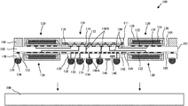
- FIG. 2 is a schematic top view illustration of a double side mounted package structure 100 structure in accordance with an embodiment.
- a memory module may include a circuit board 200 , and a double side mounted package structure 100 mounted on the circuit board 200 . This may be accomplished using flip chip bonding and solder bumps 134 .
- the double side mounted package structure 100 in accordance with embodiments may include a module substrate 102 , and a first logic die 110 mounted on a top side 103 of the module substrate 102 . While a single logic die 110 is illustrated, there may be multiple logic dies 110 . For example, multiple logic dies 110 may occupy the same perimeter illustrated by the first logic die 110 in FIG. 2 .
- a first plurality of memory packages 120 are mounted on the top side 103 of the module substrate 102 . As shown in FIG. 2 , the first plurality of memory packages 120 may optionally include a first and second groups 121 A, 121 B mounted on opposite sides of the one or more logic dies 110 .
- a second plurality of memory packages 120 are likewise mounted on a bottom side 105 of the module substrate 102 . The second plurality of memory packages 120 may be mounted directly underneath the first plurality of memory packages 120 , and likewise may be arranged in first and second groups.
- the exemplary memory packages 120 illustrated include a plurality of memory dies 124 stacked on a substrate 129 , connected with wire bonds 126 , and encapsulated in a molding material 128 . It is to be appreciated this is an exemplary implementation, and embodiments are not limited to this specific memory package configuration. In accordance with embodiments the memory packages 120 may be DRAM packages including one or more DRAM dies. Furthermore, the double side mounted package structures 100 may be implemented with a variety of memory technologies including LPDDR, LPDDR-x, HBM, HMC, etc.
- a routing substrate 130 is mounted to the bottom side 105 of the module substrate 102 and directly underneath the first logic die 110 (or multiple logic dies 110 ).
- a plurality of contacts 135 exist on a bottom side 133 of the routing substrate 130 .
- the solder bumps 134 may be placed on the contacts 135 for connection to the circuit board 200 .
- First routing is provided through the routing substrate and the coreless module substrate to connect the plurality of contacts on the bottom side of the routing substrate and the first logic die.
- general purpose in/out routing and power routing 106 A extends through the routing substrate.
- General purpose in/out routing and power routing 106 B additionally extends through the module substrate 102 .
- the general purpose in/out routing and power routing 106 A/B connect the plurality of contacts 135 on the bottom side 133 of the routing substrate 130 and the one or more logic die 110 .
- Second routing is provided within the module substrate to connect the first logic die with both the first plurality of memory packages and the second plurality of memory packages.
- signal routing 104 is located within the module substrate 102 to connect the logic die 110 with both the first plurality of memory packages 120 and the second plurality of memory packages 120 on opposite sides of the module substrate 102 .
- Length of the signal routing 104 to each memory package 120 may, for example, correspond to the memory channel length.
- memory channel length can be reduced by mounting the memory packages 120 on opposite sides of the module substrate 102 as opposed to mounting the memory packages in multiple rows, or longer rows on a same side of a substrate.
- length of the signal routing 104 can be mitigated with a reduced thickness of the module substrate 102 .
- module substrate 102 is a coreless module substrate. This may avoid requirement for the formation of vias through a substrate core. Instead, fine line patterning techniques can be utilized for all routing lines within the module substrate 102 .
- the routing substrate 130 in accordance with embodiments may be thicker than the module substrate 102 .
- the routing substrate 130 can be a laminate routing substrate, and may be a cored laminate routing substrate. This may allow for cost reduction, utilizing less expensive processing for the routing substrate 130 , which may additionally include coarser pitch, and wider line widths than the module substrate 102 . This can be achieved since the signal routing 104 between the logic die(s) 110 and memory packages 120 is contained in the module substrate 102 .
- the signal routing 104 within the module substrate 102 is characterized by a finer pitch and narrower line width than the general purpose in/out routing and the power routing 106 A through the routing substrate 130 .
- a thicker routing substrate 130 can additionally provide clearance for mounting on the circuit board 200 , as well as for placement of discrete integrated passive devices (IPDs) 140 , such as capacitor arrays, which can provide a variety of functions including voltage regulation of the general purpose in/out routing and the power routing to the logic dies 110 .
- IPDs integrated passive devices
- One or more discrete IPDs 140 can be mounted at a location such as a bottom side 133 of the routing substrate 130 laterally adjacent to the plurality of solder bumps 134 and a bottom side 105 of the module substrate 102 .
- Discrete IPDs 140 can also be located within the routing substrate 130 .
- the double side mounted package structures 100 in accordance with embodiments may include various support structures for mechanical balancing due to the thin module substrate 102 .
- the module substrate 102 may lack some mechanical robustness that would otherwise be provided by a thick core.
- Mechanical balancing may be achieved using either, or a combination of, the routing substrate 130 , stiffener ring 160 , and optionally substrate bars 150 .
- a top side stiffener ring 160 is mounted to the top side 103 of the module substrate 102 .
- the top side stiffener ring 160 may laterally surround the first plurality of memory packages 120 and the logic die(s) 110 .
- one or more substrate bars 150 are mounted to the bottom side 105 of the module substrate 102 .
- the one or more substrate bars 150 may be laterally around the second plurality of memory packages 120 and the routing substrate 130 .
- the substrate bars 150 are formed of the same substrate material as the routing substrate 130 , though this is not required.
- the substrate bars 150 may optionally be directly underneath the top side stiffener ring 160 .
- the substrate bars 150 may contain additional electrical routing.
- the substrate bars 150 may be mounted similarly as the routing substrate 130 using solder bumps 132 , optionally on contacts 155 for electrical routing.
- Solder bumps 132 may be micro bumps smaller than solder bumps 134 .
- the double side mounted package structures in accordance with embodiments can include the one or more logic die(s) 110 mounted on the top side 103 of the module substrate 102 using solder bumps 112 . As shown, solder bumps 112 may be applied to contacts 114 . The mounted logic die(s) 110 can be secured with an underfill material 118 . As shown, the logic die(s) 110 are in electrical connection with the general purpose in/out routing and power routing 106 B and signal routing 104 . The first and second pluralities of memory packages 120 may also be mounted on the top and bottom sides of the module substrate using solder bumps 122 , and the routing substrate can be mounted to the bottom side 105 of the module substrate 102 with solder bumps 132 .
- substrate bars 150 may be mounted using solder bumps 132 .
- Solder bumps 112 , 122 , 132 in accordance with embodiments may all be micro bumps and have smaller volume/area than solder bumps 134 for mounting to circuit board 200 .
- the discrete IPDs 140 may also be mounted using solder bumps 142 , which may be micro bumps of smaller volume/area than solder bumps 112 , 122 , 132 .
- the one or more logic die(s) 110 is mounted in a center of the package 100 , or module substrate 102 .
- the lateral edges 111 of the logic die 110 may be equidistant from a corresponding edge 101 of the package 100 (which may correspond to an edge of the module substrate 102 ) along one or more x-axis (illustrated by line X-X) or y-axis (illustrated by line Y-Y).
- the logic die 110 may additionally be symmetrical about the x-axis and/or y-axis.
- the one or more logic die(s) 110 is not mounted in a center of the package 110 , or module substrate 102 .
- Openings 131 may extend completely through the routing substrate 130 .
- the second plurality of memory packages 120 are mounted on the bottom side 105 of the module substrate 102 within the pair of openings 131 in the routing substrate 130 , and laterally adjacent to the routing substrate 130 .
- the routing substrate 130 may provide additional mechanical balancing and support of the thin module substrate 102 .
- the singular routing substrate 130 may negate inclusion of additional substrate bars 150 .
- FIG. 4 is yet an additional variation.
- a bottom side stiffener ring 170 is mounted to the bottom side 105 of the module substrate 102 .
- the bottom side stiffener ring 170 laterally surrounds the second plurality of memory packages 120 and the routing substrate 130 .
- the bottom side stiffener ring 170 may be identical to top side stiffener ring 160 .
- the top and bottom side stiffener rings 160 , 170 may be attached using suitable techniques including adhesive, solder, etc.
- FIG. 5 is a schematic top view illustration of a double side mounted package structure in accordance with an embodiment including multiple rows of memory packages.
- Embodiments are not limited to configurations including only first and second groups 121 A, 121 B of memory packages 120 mounted on opposite sides of the one or more logic dies 110 .
- the memory packages 120 may be placed on more than two sides of a logic die 110 , and may surround the one or more logic dies 110 .
- multiple rows of memory packages 120 may be arranged around one or more sides of a logic die 110 , and multiple rows of memory packages 120 may be arranged completely around a logic die 110 .
- the outside row, or group of memory packages 120 may be offset from the inner row, or group of memory packages 120 to allow for routing. Similar to the embodiments illustrated in FIGS. 1 and 3 the multiple rows of memory packages 120 may be mounted to both sides of the module substrate 102 .
- the bottom side memory packages may be located directly underneath the top side of memory packages as previously described.
Landscapes
- Engineering & Computer Science (AREA)
- Microelectronics & Electronic Packaging (AREA)
- Power Engineering (AREA)
- Physics & Mathematics (AREA)
- Condensed Matter Physics & Semiconductors (AREA)
- General Physics & Mathematics (AREA)
- Computer Hardware Design (AREA)
- Semiconductor Memories (AREA)
- Structures For Mounting Electric Components On Printed Circuit Boards (AREA)
Abstract
Double side mounted package structures and memory modules incorporating such double side mounted package structures are described in which memory packages are mounted on both sides of a module substrate. A routing substrate is mounted to a bottom side of the module substrate to provide general purpose in/out routing and power routing, while signal routing from the logic die to double side mounted memory packages is provided in the module routing. In an embodiment, module substrate is a coreless module substrate and may be thinner than the routing substrate.
Description
Embodiments described herein relate to multi-chip module packaging, and more particularly to memory packaging.
The current market demand for portable and mobile electronic devices such as mobile phones, personal digital assistants (PDAs), digital cameras, portable players, gaming, and other mobile devices requires the integration of more performance and features into increasingly smaller spaces. However, the amount of memory required to operate these devices has increased significantly.
Low power double data rate (LPDDR) standards have long been adopted across a variety of markets, including mobile electronics, to meet the performance and capacity requirements. LPDDR platforms and next generations (LPDDR-x) commonly include an arrangement of memory chips or packages around a logic die such as a system on chip (SOC) which may include a central processing unit (CPU) and/or graphics processing unit (GPU). In order to meet demands for increased bandwidth, various 3D solutions have been proposed that include stacked dynamic random-access memory (DRAM) dies, such as high bandwidth memory (HBM) and hybrid memory cube (HMC).
Double side mounted package structures and memory modules incorporating such double side mounted package structures are described.
In an embodiment, a double side mounted package structure includes a module substrate, a first logic die mounted on a top side of the module substrate, a first plurality of memory packages mounted on the top side of the module substrate, a second plurality of memory packages mounted on a bottom side of the module substrate, and a routing substrate mounted to the bottom side of the module substrate and directly underneath the first logic die. A plurality of contacts are located on a bottom side of the routing substrate. General purpose in/out routing and power routing are provided through the routing substrate and the module substrate to connect the plurality of contacts on the bottom side of the routing substrate and the first logic die. Signal routing is provided within the module substrate to connect the first logic die with both the first plurality of memory packages and the second plurality of memory packages.
In an embodiment, a double side mounted package structure includes a coreless module substrate, a first logic die mounted on a top side of the coreless module substrate, a first plurality of memory packages mounted on the top side of the coreless module substrate, a second plurality of memory packages mounted on a bottom side of the coreless module substrate, and a laminate routing substrate mounted to the bottom side of the coreless module substrate and directly underneath the first logic die. A plurality of contacts are located on a bottom side of the laminate routing substrate. First routing is provided through the laminate routing substrate and the coreless module substrate to connect the plurality of contacts on the bottom side of the laminate routing substrate and the first logic die. Second routing is provided within the coreless module substrate to connect the first logic die with both the first plurality of memory packages and the second plurality of memory packages.
Embodiments describe double side mounted package structures and memory modules incorporating such double side mounted package structures in which memory packages are mounted on both sides of a module substrate to reduce overall package size and memory channel length.
In one aspect, it has been observed that as memory requirements increase, the memory packages have a dramatic effect on overall multi-chip module (MCM) package size. Larger MCM packages may cause memory channel length increase and performance degradation. Furthermore, substrate yield and cycle time can be a challenge in large MCM flip chip ball grid array (FCBGA) packages due to layer count and advanced design rules.
In accordance with embodiments, the module substrates are integrated vertically to reduce memory channel length, reduce overall MCM package size and reduce MCM package height. Furthermore, the stacked integration schemes may reduce module substrate design complexity, shorten substrate cycle time, and increase substrate yield. This may be accomplished by segregating high density, complex fine pitch signal routing within a module substrate, and less critical coarser pitch board routing within the stacked routing substrate. For example, the module substrate may be a coreless or thin core substrate compared to a more traditional MCM cored substrate that may have twenty-plus layers to accommodate all the required, general purpose in/out routing, power routing, and signal routing. The segregated substrate design in accordance with embodiments may additionally allow for reduced MCM package height.
In various embodiments, description is made with reference to figures. However, certain embodiments may be practiced without one or more of these specific details, or in combination with other known methods and configurations. In the following description, numerous specific details are set forth, such as specific configurations, dimensions and processes, etc., in order to provide a thorough understanding of the embodiments. In other instances, well-known semiconductor processes and manufacturing techniques have not been described in particular detail in order to not unnecessarily obscure the embodiments. Reference throughout this specification to “one embodiment” means that a particular feature, structure, configuration, or characteristic described in connection with the embodiment is included in at least one embodiment. Thus, the appearances of the phrase “in one embodiment” in various places throughout this specification are not necessarily referring to the same embodiment. Furthermore, the particular features, structures, configurations, or characteristics may be combined in any suitable manner in one or more embodiments.
The terms “top”, “bottom”, “under”, “to”, “between”, and “on” as used herein may refer to a relative position of one layer with respect to other layers. One layer on “top”, “under”, or “on” another layer or bonded “to” or in “contact” with another layer may be directly in contact with the other layer or may have one or more intervening layers. One layer “between” layers may be directly in contact with the layers or may have one or more intervening layers.
Referring now to FIGS. 1-2 , FIG. 1 a cross-sectional side view illustration is provided of a memory module including a double side mounted package structure 100 taken along line A-A of FIG. 2 in accordance with an embodiment. FIG. 2 is a schematic top view illustration of a double side mounted package structure 100 structure in accordance with an embodiment. As illustrated, a memory module may include a circuit board 200, and a double side mounted package structure 100 mounted on the circuit board 200. This may be accomplished using flip chip bonding and solder bumps 134.
The double side mounted package structure 100 in accordance with embodiments may include a module substrate 102, and a first logic die 110 mounted on a top side 103 of the module substrate 102. While a single logic die 110 is illustrated, there may be multiple logic dies 110. For example, multiple logic dies 110 may occupy the same perimeter illustrated by the first logic die 110 in FIG. 2 . A first plurality of memory packages 120 are mounted on the top side 103 of the module substrate 102. As shown in FIG. 2 , the first plurality of memory packages 120 may optionally include a first and second groups 121A, 121B mounted on opposite sides of the one or more logic dies 110. A second plurality of memory packages 120 are likewise mounted on a bottom side 105 of the module substrate 102. The second plurality of memory packages 120 may be mounted directly underneath the first plurality of memory packages 120, and likewise may be arranged in first and second groups.
The exemplary memory packages 120 illustrated include a plurality of memory dies 124 stacked on a substrate 129, connected with wire bonds 126, and encapsulated in a molding material 128. It is to be appreciated this is an exemplary implementation, and embodiments are not limited to this specific memory package configuration. In accordance with embodiments the memory packages 120 may be DRAM packages including one or more DRAM dies. Furthermore, the double side mounted package structures 100 may be implemented with a variety of memory technologies including LPDDR, LPDDR-x, HBM, HMC, etc.
Referring again to FIG. 1 , a routing substrate 130 is mounted to the bottom side 105 of the module substrate 102 and directly underneath the first logic die 110 (or multiple logic dies 110). A plurality of contacts 135 exist on a bottom side 133 of the routing substrate 130. The solder bumps 134 may be placed on the contacts 135 for connection to the circuit board 200.
First routing is provided through the routing substrate and the coreless module substrate to connect the plurality of contacts on the bottom side of the routing substrate and the first logic die. In an embodiment, general purpose in/out routing and power routing 106A extends through the routing substrate. General purpose in/out routing and power routing 106B additionally extends through the module substrate 102. Together, the general purpose in/out routing and power routing 106A/B connect the plurality of contacts 135 on the bottom side 133 of the routing substrate 130 and the one or more logic die 110.
Second routing is provided within the module substrate to connect the first logic die with both the first plurality of memory packages and the second plurality of memory packages. In an embodiment signal routing 104 is located within the module substrate 102 to connect the logic die 110 with both the first plurality of memory packages 120 and the second plurality of memory packages 120 on opposite sides of the module substrate 102. Length of the signal routing 104 to each memory package 120 may, for example, correspond to the memory channel length. Thus, memory channel length can be reduced by mounting the memory packages 120 on opposite sides of the module substrate 102 as opposed to mounting the memory packages in multiple rows, or longer rows on a same side of a substrate. Furthermore, length of the signal routing 104 can be mitigated with a reduced thickness of the module substrate 102. In some embodiments, module substrate 102 is a coreless module substrate. This may avoid requirement for the formation of vias through a substrate core. Instead, fine line patterning techniques can be utilized for all routing lines within the module substrate 102.
The routing substrate 130 in accordance with embodiments may be thicker than the module substrate 102. In some embodiments, the routing substrate 130 can be a laminate routing substrate, and may be a cored laminate routing substrate. This may allow for cost reduction, utilizing less expensive processing for the routing substrate 130, which may additionally include coarser pitch, and wider line widths than the module substrate 102. This can be achieved since the signal routing 104 between the logic die(s) 110 and memory packages 120 is contained in the module substrate 102. Thus, the signal routing 104 within the module substrate 102 is characterized by a finer pitch and narrower line width than the general purpose in/out routing and the power routing 106A through the routing substrate 130. A thicker routing substrate 130 can additionally provide clearance for mounting on the circuit board 200, as well as for placement of discrete integrated passive devices (IPDs) 140, such as capacitor arrays, which can provide a variety of functions including voltage regulation of the general purpose in/out routing and the power routing to the logic dies 110. One or more discrete IPDs 140 can be mounted at a location such as a bottom side 133 of the routing substrate 130 laterally adjacent to the plurality of solder bumps 134 and a bottom side 105 of the module substrate 102. Discrete IPDs 140 can also be located within the routing substrate 130.
The double side mounted package structures 100 in accordance with embodiments may include various support structures for mechanical balancing due to the thin module substrate 102. For example, the module substrate 102 may lack some mechanical robustness that would otherwise be provided by a thick core. Mechanical balancing may be achieved using either, or a combination of, the routing substrate 130, stiffener ring 160, and optionally substrate bars 150. In the embodiments illustrated in FIGS. 1-2 a top side stiffener ring 160 is mounted to the top side 103 of the module substrate 102. The top side stiffener ring 160 may laterally surround the first plurality of memory packages 120 and the logic die(s) 110.
In the embodiment illustrated in FIG. 1 , one or more substrate bars 150 are mounted to the bottom side 105 of the module substrate 102. The one or more substrate bars 150 may be laterally around the second plurality of memory packages 120 and the routing substrate 130. In an embodiment, the substrate bars 150 are formed of the same substrate material as the routing substrate 130, though this is not required. The substrate bars 150, may optionally be directly underneath the top side stiffener ring 160. In an embodiment, the substrate bars 150 may contain additional electrical routing. Thus, the substrate bars 150 may be mounted similarly as the routing substrate 130 using solder bumps 132, optionally on contacts 155 for electrical routing. Solder bumps 132 may be micro bumps smaller than solder bumps 134.
The double side mounted package structures in accordance with embodiments can include the one or more logic die(s) 110 mounted on the top side 103 of the module substrate 102 using solder bumps 112. As shown, solder bumps 112 may be applied to contacts 114. The mounted logic die(s) 110 can be secured with an underfill material 118. As shown, the logic die(s) 110 are in electrical connection with the general purpose in/out routing and power routing 106B and signal routing 104. The first and second pluralities of memory packages 120 may also be mounted on the top and bottom sides of the module substrate using solder bumps 122, and the routing substrate can be mounted to the bottom side 105 of the module substrate 102 with solder bumps 132. Similarly, substrate bars 150 may be mounted using solder bumps 132. Solder bumps 112, 122, 132 in accordance with embodiments may all be micro bumps and have smaller volume/area than solder bumps 134 for mounting to circuit board 200. Furthermore, the discrete IPDs 140 may also be mounted using solder bumps 142, which may be micro bumps of smaller volume/area than solder bumps 112, 122, 132.
In an embodiment such as that illustrated in FIG. 2 the one or more logic die(s) 110 is mounted in a center of the package 100, or module substrate 102. For example, the lateral edges 111 of the logic die 110 may be equidistant from a corresponding edge 101 of the package 100 (which may correspond to an edge of the module substrate 102) along one or more x-axis (illustrated by line X-X) or y-axis (illustrated by line Y-Y). The logic die 110 may additionally be symmetrical about the x-axis and/or y-axis. In another embodiment, the one or more logic die(s) 110 is not mounted in a center of the package 110, or module substrate 102.
Referring now to FIG. 3 a schematic top view illustration is provided of openings 131 within a routing substrate 130 in accordance with an embodiment. Openings 131 may extend completely through the routing substrate 130. In such a variation, the second plurality of memory packages 120 are mounted on the bottom side 105 of the module substrate 102 within the pair of openings 131 in the routing substrate 130, and laterally adjacent to the routing substrate 130. In this manner, the routing substrate 130 may provide additional mechanical balancing and support of the thin module substrate 102. Thus, the singular routing substrate 130 may negate inclusion of additional substrate bars 150.
Up until this point various structural configurations have been described in which memory channel length can be reduced by mounting the memory packages 120 on opposite sides of the module substrate 102 as opposed to mounting the memory packages in multiple rows, or longer rows on a same side of a substrate. However, the double side mounted MCM package structures are additionally compatible with such configuration, particularly for larger memory scaling. FIG. 5 is a schematic top view illustration of a double side mounted package structure in accordance with an embodiment including multiple rows of memory packages. Embodiments are not limited to configurations including only first and second groups 121A, 121B of memory packages 120 mounted on opposite sides of the one or more logic dies 110. As shown, the memory packages 120 may be placed on more than two sides of a logic die 110, and may surround the one or more logic dies 110. Furthermore, multiple rows of memory packages 120 may be arranged around one or more sides of a logic die 110, and multiple rows of memory packages 120 may be arranged completely around a logic die 110. In the embodiment illustrated, the outside row, or group of memory packages 120 may be offset from the inner row, or group of memory packages 120 to allow for routing. Similar to the embodiments illustrated in FIGS. 1 and 3 the multiple rows of memory packages 120 may be mounted to both sides of the module substrate 102. Furthermore, the bottom side memory packages may be located directly underneath the top side of memory packages as previously described.
In utilizing the various aspects of the embodiments, it would become apparent to one skilled in the art that combinations or variations of the above embodiments are possible for forming an double side mounted MCM package. Although the embodiments have been described in language specific to structural features and/or methodological acts, it is to be understood that the appended claims are not necessarily limited to the specific features or acts described. The specific features and acts disclosed are instead to be understood as embodiments of the claims useful for illustration.
Claims (21)
1. A double side mounted package structure comprising:
a module substrate;
a first logic die mounted on a top side of the module substrate;
a first plurality of memory packages mounted on the top side of the module substrate;
a second plurality of memory packages mounted on a bottom side of the module substrate;
a routing substrate mounted to the bottom side of the module substrate and directly underneath the first logic die;
a plurality of contacts on a bottom side of the routing substrate;
general purpose in/out routing and power routing through the routing substrate and the module substrate to connect the plurality of contacts on the bottom side of the routing substrate and the first logic die; and
signal routing within the module substrate to connect the first logic die with both the first plurality of memory packages and the second plurality of memory packages;
wherein the signal routing within the module substrate is characterized by a finer pitch and narrower line width than the general purpose in/out routing and the power routing through the routing substrate.
2. The double side mounted package structure of claim 1 , further comprising a top side stiffener ring mounted to the top side of the module substrate, wherein the top side stiffener ring laterally surrounds the first plurality of memory packages and the first logic die.
3. The double side mounted package structure of claim 2 , further comprising a bottom side stiffener ring mounted to the bottom side of the module substrate, wherein the bottom side stiffener ring laterally surrounds the second plurality of memory packages and the routing substrate.
4. The double side mounted package structure of claim 2 , further comprising one or more substrate bars mounted to the bottom side of the module substrate, wherein the one or more substrate bars are laterally around the second plurality of memory packages and the routing substrate.
5. The double side mounted package structure of claim 1 , further comprising a pair of openings in the routing substrate, wherein the second plurality of memory packages are mounted on the bottom side of the module substrate within the pair of openings in the routing substrate.
6. The double side mounted package structure of claim 5 , wherein the second plurality of memory packages are directly underneath the first plurality of memory packages.
7. The double side mounted package structure of claim 1 , further comprising a plurality of solder bumps on a bottom side of the routing substrate.
8. The double side mounted package structure of claim 7 , wherein:
the first logic die is mounted on the top side of the module substrate with solder bumps;
the first plurality of memory packages is mounted on the top side of the module substrate with solder bumps;
the second plurality of memory packages is mounted on the bottom side of the module substrate with solder bumps; and
the routing substrate is mounted to the bottom side of the module substrate with solder bumps.
9. The double side mounted package structure of claim 8 , further comprising a discrete integrated passive device component mounted at a location selected from the group consisting of the bottom side of the routing substrate laterally adjacent to the plurality of solder bumps, a bottom side of the module substrate, and within the routing substrate.
10. A double side mounted package structure comprising:
a coreless module substrate;
a first logic die mounted on a top side of the coreless module substrate;
a first plurality of memory packages mounted on the top side of the coreless module substrate;
a second plurality of memory packages mounted on a bottom side of the coreless module substrate;
a laminate routing substrate mounted to the bottom side of the coreless module substrate and directly underneath the first logic die, wherein the laminate routing substrate is thicker than the coreless module substrate;
a plurality of contacts on a bottom side of the laminate routing substrate;
first routing through the laminate routing substrate and the coreless module substrate to connect the plurality of contacts on the bottom side of the laminate routing substrate and the first logic die; and
second routing within the coreless module substrate to connect the first logic die with both the first plurality of memory packages and the second plurality of memory packages.
11. The double side mounted package structure of claim 10 , wherein the laminate routing substrate is a cored substrate.
12. The double side mounted package structure of claim 10 , wherein the second routing within the coreless module substrate is characterized by a finer pitch and narrower line width than the first routing through the laminate routing substrate.
13. The double side mounted package structure of claim 10 , further comprising a top side stiffener ring mounted to the top side of the coreless module substrate, wherein the top side stiffener ring laterally surrounds the first plurality of memory packages and the first logic die.
14. The double side mounted package structure of claim 13 , further comprising a bottom side stiffener ring mounted to the bottom side of the coreless module substrate, wherein the bottom side stiffener ring laterally surrounds the second plurality of memory packages and the laminate routing substrate.
15. The double side mounted package structure of claim 10 , further comprising a pair of openings in the laminate routing substrate, wherein the second plurality of memory packages are mounted on the bottom side of the coreless module substrate within the pair of openings in the laminate routing substrate.
16. The double side mounted package structure of claim 15 , wherein the second plurality of memory packages are directly underneath the first plurality of memory packages.
17. The double side mounted package structure of claim 10 , further comprising a plurality of solder bumps on a bottom side of the laminate routing substrate.
18. The double side mounted package structure of claim 17 , further comprising a discrete integrated passive device component mounted at a location selected from the group consisting of the bottom side of the laminate routing substrate laterally adjacent to the plurality of solder bumps, a bottom side of the coreless module substrate, and within the laminate routing substrate.
19. A memory module comprising:
a circuit board;
a double side mounted package structure mounted on the circuit board, the double side mounted package structure comprising:
a module substrate;
a first logic die mounted on a top side of the module substrate;
a first plurality of memory packages mounted on the top side of the module substrate;
a second plurality of memory packages mounted on a bottom side of the module substrate; and
a routing substrate mounted to the bottom side of the module substrate and directly underneath the first logic die, wherein the routing substrate is thicker than the module substrate;
a plurality of contacts on a bottom side of the routing substrate;
general purpose in/out routing and power routing through the routing substrate and the module substrate to connect the plurality of contacts on the bottom side of the routing substrate and the first logic die; and
signal routing within the module substrate to connect the first logic die with both the first plurality of memory packages and the second plurality of memory packages.
20. The memory module of claim 19 , wherein the module substrate is a coreless module substrate.
21. The memory module of claim 20 , wherein the routing substrate is a cored laminate substrate.
Priority Applications (5)
| Application Number | Priority Date | Filing Date | Title |
|---|---|---|---|
| US16/204,679 US10685948B1 (en) | 2018-11-29 | 2018-11-29 | Double side mounted large MCM package with memory channel length reduction |
| PCT/US2019/062701 WO2020112504A1 (en) | 2018-11-29 | 2019-11-21 | Double side mounted large mcm package with memory channel length reduction |
| CN201980079413.4A CN113169157B (en) | 2018-11-29 | 2019-11-21 | Double-sided mounted large MCM package with reduced memory channel length |
| TW108143068A TWI734271B (en) | 2018-11-29 | 2019-11-27 | Double side mounted large mcm package with memory channel length reduction |
| US16/880,463 US11158621B2 (en) | 2018-11-29 | 2020-05-21 | Double side mounted large MCM package with memory channel length reduction |
Applications Claiming Priority (1)
| Application Number | Priority Date | Filing Date | Title |
|---|---|---|---|
| US16/204,679 US10685948B1 (en) | 2018-11-29 | 2018-11-29 | Double side mounted large MCM package with memory channel length reduction |
Related Child Applications (1)
| Application Number | Title | Priority Date | Filing Date |
|---|---|---|---|
| US16/880,463 Continuation US11158621B2 (en) | 2018-11-29 | 2020-05-21 | Double side mounted large MCM package with memory channel length reduction |
Publications (2)
| Publication Number | Publication Date |
|---|---|
| US20200176431A1 US20200176431A1 (en) | 2020-06-04 |
| US10685948B1 true US10685948B1 (en) | 2020-06-16 |
Family
ID=69024592
Family Applications (2)
| Application Number | Title | Priority Date | Filing Date |
|---|---|---|---|
| US16/204,679 Active US10685948B1 (en) | 2018-11-29 | 2018-11-29 | Double side mounted large MCM package with memory channel length reduction |
| US16/880,463 Active US11158621B2 (en) | 2018-11-29 | 2020-05-21 | Double side mounted large MCM package with memory channel length reduction |
Family Applications After (1)
| Application Number | Title | Priority Date | Filing Date |
|---|---|---|---|
| US16/880,463 Active US11158621B2 (en) | 2018-11-29 | 2020-05-21 | Double side mounted large MCM package with memory channel length reduction |
Country Status (4)
| Country | Link |
|---|---|
| US (2) | US10685948B1 (en) |
| CN (1) | CN113169157B (en) |
| TW (1) | TWI734271B (en) |
| WO (1) | WO2020112504A1 (en) |
Cited By (1)
| Publication number | Priority date | Publication date | Assignee | Title |
|---|---|---|---|---|
| US11908810B2 (en) | 2020-12-03 | 2024-02-20 | Samsung Electronics Co., Ltd. | Hybrid semiconductor device and electronic device |
Families Citing this family (3)
| Publication number | Priority date | Publication date | Assignee | Title |
|---|---|---|---|---|
| US20190157253A1 (en) * | 2019-01-22 | 2019-05-23 | Intel Corporation | Circuit Systems Having Memory Modules With Reverse Orientations |
| KR20210075270A (en) * | 2019-12-12 | 2021-06-23 | 삼성전자주식회사 | Semiconductor module |
| US20230420351A1 (en) * | 2022-06-28 | 2023-12-28 | Applied Materials, Inc. | Substrate frame design for three-dimensional stacked electronic assemblies |
Citations (11)
| Publication number | Priority date | Publication date | Assignee | Title |
|---|---|---|---|---|
| US20110140268A1 (en) | 2009-12-16 | 2011-06-16 | Bok Eng Cheah | High-density inter-package connections for ultra-thin package-on-package structures, and processes of forming same |
| US20120250265A1 (en) | 2009-12-22 | 2012-10-04 | Murata Manufacturing Co., Ltd. | Circuit module manufacturing method, circuit module, and electronic apparatus including circuit module |
| US9153550B2 (en) * | 2013-11-14 | 2015-10-06 | Taiwan Semiconductor Manufacturing Company, Ltd. | Substrate design with balanced metal and solder resist density |
| US20160071818A1 (en) | 2014-09-05 | 2016-03-10 | Invensas Corporation | Multichip modules and methods of fabrication |
| US20160329272A1 (en) | 2014-12-19 | 2016-11-10 | Intel IP Corporation | Stacked semiconductor device package with improved interconnect bandwidth |
| US20160372448A1 (en) * | 2015-05-20 | 2016-12-22 | Broadpak Corporation | Semiconductor structure and a method of making thereof |
| WO2017111975A1 (en) | 2015-12-22 | 2017-06-29 | Intel Corporation | Microelectronic devices with high frequency communication modules having compound semiconductor devices integrated on a package fabric |
| US20170263518A1 (en) | 2016-03-11 | 2017-09-14 | Taiwan Semiconductor Manufacturing Company, Ltd. | Integrated Fan-Out Package Including Voltage Regulators and Methods Forming Same |
| US9818680B2 (en) * | 2011-07-27 | 2017-11-14 | Broadpak Corporation | Scalable semiconductor interposer integration |
| US9997231B2 (en) | 2013-08-09 | 2018-06-12 | Renesas Electronics Corporation | Electronic device |
| US20180182734A1 (en) | 2016-12-28 | 2018-06-28 | Intel Corporation | Methods of forming package structures for enhanced memory capacity and structures formed thereby |
Family Cites Families (3)
| Publication number | Priority date | Publication date | Assignee | Title |
|---|---|---|---|---|
| US6678167B1 (en) | 2000-02-04 | 2004-01-13 | Agere Systems Inc | High performance multi-chip IC package |
| JP3461172B2 (en) * | 2001-07-05 | 2003-10-27 | 日東電工株式会社 | Method for manufacturing multilayer wiring circuit board |
| KR101274460B1 (en) * | 2011-11-22 | 2013-06-18 | 삼성전기주식회사 | Semiconductor package and manufacturing method threrof |
-
2018
- 2018-11-29 US US16/204,679 patent/US10685948B1/en active Active
-
2019
- 2019-11-21 WO PCT/US2019/062701 patent/WO2020112504A1/en active Application Filing
- 2019-11-21 CN CN201980079413.4A patent/CN113169157B/en active Active
- 2019-11-27 TW TW108143068A patent/TWI734271B/en active
-
2020
- 2020-05-21 US US16/880,463 patent/US11158621B2/en active Active
Patent Citations (11)
| Publication number | Priority date | Publication date | Assignee | Title |
|---|---|---|---|---|
| US20110140268A1 (en) | 2009-12-16 | 2011-06-16 | Bok Eng Cheah | High-density inter-package connections for ultra-thin package-on-package structures, and processes of forming same |
| US20120250265A1 (en) | 2009-12-22 | 2012-10-04 | Murata Manufacturing Co., Ltd. | Circuit module manufacturing method, circuit module, and electronic apparatus including circuit module |
| US9818680B2 (en) * | 2011-07-27 | 2017-11-14 | Broadpak Corporation | Scalable semiconductor interposer integration |
| US9997231B2 (en) | 2013-08-09 | 2018-06-12 | Renesas Electronics Corporation | Electronic device |
| US9153550B2 (en) * | 2013-11-14 | 2015-10-06 | Taiwan Semiconductor Manufacturing Company, Ltd. | Substrate design with balanced metal and solder resist density |
| US20160071818A1 (en) | 2014-09-05 | 2016-03-10 | Invensas Corporation | Multichip modules and methods of fabrication |
| US20160329272A1 (en) | 2014-12-19 | 2016-11-10 | Intel IP Corporation | Stacked semiconductor device package with improved interconnect bandwidth |
| US20160372448A1 (en) * | 2015-05-20 | 2016-12-22 | Broadpak Corporation | Semiconductor structure and a method of making thereof |
| WO2017111975A1 (en) | 2015-12-22 | 2017-06-29 | Intel Corporation | Microelectronic devices with high frequency communication modules having compound semiconductor devices integrated on a package fabric |
| US20170263518A1 (en) | 2016-03-11 | 2017-09-14 | Taiwan Semiconductor Manufacturing Company, Ltd. | Integrated Fan-Out Package Including Voltage Regulators and Methods Forming Same |
| US20180182734A1 (en) | 2016-12-28 | 2018-06-28 | Intel Corporation | Methods of forming package structures for enhanced memory capacity and structures formed thereby |
Non-Patent Citations (1)
| Title |
|---|
| International Search Report and Written Opinion of International Application No. PCT/US2019/062701 dated Mar. 4, 2020, 14 pages. |
Cited By (1)
| Publication number | Priority date | Publication date | Assignee | Title |
|---|---|---|---|---|
| US11908810B2 (en) | 2020-12-03 | 2024-02-20 | Samsung Electronics Co., Ltd. | Hybrid semiconductor device and electronic device |
Also Published As
| Publication number | Publication date |
|---|---|
| US20200279842A1 (en) | 2020-09-03 |
| US11158621B2 (en) | 2021-10-26 |
| TW202040787A (en) | 2020-11-01 |
| TWI734271B (en) | 2021-07-21 |
| US20200176431A1 (en) | 2020-06-04 |
| WO2020112504A1 (en) | 2020-06-04 |
| CN113169157B (en) | 2023-10-27 |
| CN113169157A (en) | 2021-07-23 |
Similar Documents
| Publication | Publication Date | Title |
|---|---|---|
| US11158621B2 (en) | Double side mounted large MCM package with memory channel length reduction | |
| US7872340B2 (en) | Integrated circuit package system employing an offset stacked configuration | |
| US7368319B2 (en) | Stacked integrated circuit package-in-package system | |
| US8063475B2 (en) | Semiconductor package system with through silicon via interposer | |
| US8987896B2 (en) | High-density inter-package connections for ultra-thin package-on-package structures, and processes of forming same | |
| US7977579B2 (en) | Multiple flip-chip integrated circuit package system | |
| US8026129B2 (en) | Stacked integrated circuits package system with passive components | |
| US8089143B2 (en) | Integrated circuit package system using interposer | |
| US7420269B2 (en) | Stacked integrated circuit package-in-package system | |
| US7498667B2 (en) | Stacked integrated circuit package-in-package system | |
| US8723302B2 (en) | Integrated circuit package system with input/output expansion | |
| US7560818B2 (en) | Stacked structure of chips and water structure for making the same | |
| US20080227238A1 (en) | Integrated circuit package system employing multi-package module techniques | |
| US20120326331A1 (en) | Integrated circuit packaging system with vertical interconnects and method of manufacture thereof | |
| US20100155919A1 (en) | High-density multifunctional PoP-type multi-chip package structure | |
| KR20210101802A (en) | Semiconductor packages and method of manufacturing semiconductor packages | |
| US7687920B2 (en) | Integrated circuit package-on-package system with central bond wires | |
| US8304337B2 (en) | Integrated circuit packaging system with bond wire pads and method of manufacture thereof | |
| KR20140028209A (en) | Semiconductor chip, semiconductor stack package having the chip and chip selection method for the same | |
| US9318470B2 (en) | Semiconductor device | |
| KR100851108B1 (en) | Wafer level system in package and fabrication method thereof | |
| KR20120023972A (en) | Semiconductor chip and stacked semiconductor package having the same | |
| KR20060128376A (en) | Chip stack package | |
| KR20060074091A (en) | Chip stack package | |
| CN117747557A (en) | Multi-die stacked package |
Legal Events
| Date | Code | Title | Description |
|---|---|---|---|
| FEPP | Fee payment procedure |
Free format text: ENTITY STATUS SET TO UNDISCOUNTED (ORIGINAL EVENT CODE: BIG.); ENTITY STATUS OF PATENT OWNER: LARGE ENTITY |
|
| STCF | Information on status: patent grant |
Free format text: PATENTED CASE |
|
| CC | Certificate of correction | ||
| MAFP | Maintenance fee payment |
Free format text: PAYMENT OF MAINTENANCE FEE, 4TH YEAR, LARGE ENTITY (ORIGINAL EVENT CODE: M1551); ENTITY STATUS OF PATENT OWNER: LARGE ENTITY Year of fee payment: 4 |