US10680091B2 - Semiconductor device - Google Patents
Semiconductor device Download PDFInfo
- Publication number
- US10680091B2 US10680091B2 US16/229,613 US201816229613A US10680091B2 US 10680091 B2 US10680091 B2 US 10680091B2 US 201816229613 A US201816229613 A US 201816229613A US 10680091 B2 US10680091 B2 US 10680091B2
- Authority
- US
- United States
- Prior art keywords
- semiconductor
- layer
- gas layer
- gate
- laminated body
- Prior art date
- Legal status (The legal status is an assumption and is not a legal conclusion. Google has not performed a legal analysis and makes no representation as to the accuracy of the status listed.)
- Active
Links
Images


Classifications
-
- H—ELECTRICITY
- H10—SEMICONDUCTOR DEVICES; ELECTRIC SOLID-STATE DEVICES NOT OTHERWISE PROVIDED FOR
- H10D—INORGANIC ELECTRIC SEMICONDUCTOR DEVICES
- H10D62/00—Semiconductor bodies, or regions thereof, of devices having potential barriers
- H10D62/10—Shapes, relative sizes or dispositions of the regions of the semiconductor bodies; Shapes of the semiconductor bodies
- H10D62/124—Shapes, relative sizes or dispositions of the regions of semiconductor bodies or of junctions between the regions
-
- H01L29/7782—
-
- H—ELECTRICITY
- H10—SEMICONDUCTOR DEVICES; ELECTRIC SOLID-STATE DEVICES NOT OTHERWISE PROVIDED FOR
- H10D—INORGANIC ELECTRIC SEMICONDUCTOR DEVICES
- H10D30/00—Field-effect transistors [FET]
- H10D30/40—FETs having zero-dimensional [0D], one-dimensional [1D] or two-dimensional [2D] charge carrier gas channels
- H10D30/47—FETs having zero-dimensional [0D], one-dimensional [1D] or two-dimensional [2D] charge carrier gas channels having two-dimensional [2D] charge carrier gas channels, e.g. nanoribbon FETs or high electron mobility transistors [HEMT]
- H10D30/471—High electron mobility transistors [HEMT] or high hole mobility transistors [HHMT]
- H10D30/473—High electron mobility transistors [HEMT] or high hole mobility transistors [HHMT] having confinement of carriers by multiple heterojunctions, e.g. quantum well HEMT
-
- H01L29/0649—
-
- H01L29/0847—
-
- H01L29/0891—
-
- H01L29/1066—
-
- H01L29/365—
-
- H01L29/41766—
-
- H01L29/42316—
-
- H01L29/778—
-
- H01L29/7789—
-
- H—ELECTRICITY
- H10—SEMICONDUCTOR DEVICES; ELECTRIC SOLID-STATE DEVICES NOT OTHERWISE PROVIDED FOR
- H10D—INORGANIC ELECTRIC SEMICONDUCTOR DEVICES
- H10D30/00—Field-effect transistors [FET]
- H10D30/01—Manufacture or treatment
- H10D30/015—Manufacture or treatment of FETs having heterojunction interface channels or heterojunction gate electrodes, e.g. HEMT
-
- H—ELECTRICITY
- H10—SEMICONDUCTOR DEVICES; ELECTRIC SOLID-STATE DEVICES NOT OTHERWISE PROVIDED FOR
- H10D—INORGANIC ELECTRIC SEMICONDUCTOR DEVICES
- H10D30/00—Field-effect transistors [FET]
- H10D30/40—FETs having zero-dimensional [0D], one-dimensional [1D] or two-dimensional [2D] charge carrier gas channels
- H10D30/47—FETs having zero-dimensional [0D], one-dimensional [1D] or two-dimensional [2D] charge carrier gas channels having two-dimensional [2D] charge carrier gas channels, e.g. nanoribbon FETs or high electron mobility transistors [HEMT]
- H10D30/471—High electron mobility transistors [HEMT] or high hole mobility transistors [HHMT]
- H10D30/473—High electron mobility transistors [HEMT] or high hole mobility transistors [HHMT] having confinement of carriers by multiple heterojunctions, e.g. quantum well HEMT
- H10D30/4732—High electron mobility transistors [HEMT] or high hole mobility transistors [HHMT] having confinement of carriers by multiple heterojunctions, e.g. quantum well HEMT using Group III-V semiconductor material
-
- H—ELECTRICITY
- H10—SEMICONDUCTOR DEVICES; ELECTRIC SOLID-STATE DEVICES NOT OTHERWISE PROVIDED FOR
- H10D—INORGANIC ELECTRIC SEMICONDUCTOR DEVICES
- H10D30/00—Field-effect transistors [FET]
- H10D30/40—FETs having zero-dimensional [0D], one-dimensional [1D] or two-dimensional [2D] charge carrier gas channels
- H10D30/47—FETs having zero-dimensional [0D], one-dimensional [1D] or two-dimensional [2D] charge carrier gas channels having two-dimensional [2D] charge carrier gas channels, e.g. nanoribbon FETs or high electron mobility transistors [HEMT]
- H10D30/471—High electron mobility transistors [HEMT] or high hole mobility transistors [HHMT]
- H10D30/478—High electron mobility transistors [HEMT] or high hole mobility transistors [HHMT] the 2D charge carrier gas being at least partially not parallel to a main surface of the semiconductor body
-
- H—ELECTRICITY
- H10—SEMICONDUCTOR DEVICES; ELECTRIC SOLID-STATE DEVICES NOT OTHERWISE PROVIDED FOR
- H10D—INORGANIC ELECTRIC SEMICONDUCTOR DEVICES
- H10D62/00—Semiconductor bodies, or regions thereof, of devices having potential barriers
- H10D62/10—Shapes, relative sizes or dispositions of the regions of the semiconductor bodies; Shapes of the semiconductor bodies
- H10D62/102—Constructional design considerations for preventing surface leakage or controlling electric field concentration
- H10D62/103—Constructional design considerations for preventing surface leakage or controlling electric field concentration for increasing or controlling the breakdown voltage of reverse-biased devices
- H10D62/105—Constructional design considerations for preventing surface leakage or controlling electric field concentration for increasing or controlling the breakdown voltage of reverse-biased devices by having particular doping profiles, shapes or arrangements of PN junctions; by having supplementary regions, e.g. junction termination extension [JTE]
- H10D62/109—Reduced surface field [RESURF] PN junction structures
- H10D62/111—Multiple RESURF structures, e.g. double RESURF or 3D-RESURF structures
-
- H—ELECTRICITY
- H10—SEMICONDUCTOR DEVICES; ELECTRIC SOLID-STATE DEVICES NOT OTHERWISE PROVIDED FOR
- H10D—INORGANIC ELECTRIC SEMICONDUCTOR DEVICES
- H10D62/00—Semiconductor bodies, or regions thereof, of devices having potential barriers
- H10D62/10—Shapes, relative sizes or dispositions of the regions of the semiconductor bodies; Shapes of the semiconductor bodies
- H10D62/113—Isolations within a component, i.e. internal isolations
- H10D62/115—Dielectric isolations, e.g. air gaps
-
- H—ELECTRICITY
- H10—SEMICONDUCTOR DEVICES; ELECTRIC SOLID-STATE DEVICES NOT OTHERWISE PROVIDED FOR
- H10D—INORGANIC ELECTRIC SEMICONDUCTOR DEVICES
- H10D62/00—Semiconductor bodies, or regions thereof, of devices having potential barriers
- H10D62/10—Shapes, relative sizes or dispositions of the regions of the semiconductor bodies; Shapes of the semiconductor bodies
- H10D62/13—Semiconductor regions connected to electrodes carrying current to be rectified, amplified or switched, e.g. source or drain regions
- H10D62/149—Source or drain regions of field-effect devices
- H10D62/151—Source or drain regions of field-effect devices of IGFETs
-
- H—ELECTRICITY
- H10—SEMICONDUCTOR DEVICES; ELECTRIC SOLID-STATE DEVICES NOT OTHERWISE PROVIDED FOR
- H10D—INORGANIC ELECTRIC SEMICONDUCTOR DEVICES
- H10D62/00—Semiconductor bodies, or regions thereof, of devices having potential barriers
- H10D62/10—Shapes, relative sizes or dispositions of the regions of the semiconductor bodies; Shapes of the semiconductor bodies
- H10D62/13—Semiconductor regions connected to electrodes carrying current to be rectified, amplified or switched, e.g. source or drain regions
- H10D62/149—Source or drain regions of field-effect devices
- H10D62/161—Source or drain regions of field-effect devices of FETs having Schottky gates
-
- H—ELECTRICITY
- H10—SEMICONDUCTOR DEVICES; ELECTRIC SOLID-STATE DEVICES NOT OTHERWISE PROVIDED FOR
- H10D—INORGANIC ELECTRIC SEMICONDUCTOR DEVICES
- H10D62/00—Semiconductor bodies, or regions thereof, of devices having potential barriers
- H10D62/10—Shapes, relative sizes or dispositions of the regions of the semiconductor bodies; Shapes of the semiconductor bodies
- H10D62/17—Semiconductor regions connected to electrodes not carrying current to be rectified, amplified or switched, e.g. channel regions
- H10D62/343—Gate regions of field-effect devices having PN junction gates
-
- H—ELECTRICITY
- H10—SEMICONDUCTOR DEVICES; ELECTRIC SOLID-STATE DEVICES NOT OTHERWISE PROVIDED FOR
- H10D—INORGANIC ELECTRIC SEMICONDUCTOR DEVICES
- H10D62/00—Semiconductor bodies, or regions thereof, of devices having potential barriers
- H10D62/60—Impurity distributions or concentrations
- H10D62/605—Planar doped, e.g. atomic-plane doped or delta-doped
-
- H—ELECTRICITY
- H10—SEMICONDUCTOR DEVICES; ELECTRIC SOLID-STATE DEVICES NOT OTHERWISE PROVIDED FOR
- H10D—INORGANIC ELECTRIC SEMICONDUCTOR DEVICES
- H10D64/00—Electrodes of devices having potential barriers
- H10D64/20—Electrodes characterised by their shapes, relative sizes or dispositions
- H10D64/23—Electrodes carrying the current to be rectified, amplified, oscillated or switched, e.g. sources, drains, anodes or cathodes
- H10D64/251—Source or drain electrodes for field-effect devices
- H10D64/256—Source or drain electrodes for field-effect devices for lateral devices wherein the source or drain electrodes are recessed in semiconductor bodies
-
- H—ELECTRICITY
- H10—SEMICONDUCTOR DEVICES; ELECTRIC SOLID-STATE DEVICES NOT OTHERWISE PROVIDED FOR
- H10D—INORGANIC ELECTRIC SEMICONDUCTOR DEVICES
- H10D64/00—Electrodes of devices having potential barriers
- H10D64/20—Electrodes characterised by their shapes, relative sizes or dispositions
- H10D64/27—Electrodes not carrying the current to be rectified, amplified, oscillated or switched, e.g. gates
- H10D64/311—Gate electrodes for field-effect devices
- H10D64/411—Gate electrodes for field-effect devices for FETs
- H10D64/511—Gate electrodes for field-effect devices for FETs for IGFETs
- H10D64/512—Disposition of the gate electrodes, e.g. buried gates
- H10D64/513—Disposition of the gate electrodes, e.g. buried gates within recesses in the substrate, e.g. trench gates, groove gates or buried gates
-
- H01L29/20—
-
- H01L29/2003—
-
- H—ELECTRICITY
- H10—SEMICONDUCTOR DEVICES; ELECTRIC SOLID-STATE DEVICES NOT OTHERWISE PROVIDED FOR
- H10D—INORGANIC ELECTRIC SEMICONDUCTOR DEVICES
- H10D62/00—Semiconductor bodies, or regions thereof, of devices having potential barriers
- H10D62/80—Semiconductor bodies, or regions thereof, of devices having potential barriers characterised by the materials
- H10D62/85—Semiconductor bodies, or regions thereof, of devices having potential barriers characterised by the materials being Group III-V materials, e.g. GaAs
- H10D62/8503—Nitride Group III-V materials, e.g. AlN or GaN
Definitions
- the technology disclosed in this specification relates to a semiconductor device having a heterojunction type superjunction structure.
- the two-dimensional hole gas layer of the semiconductor laminated body is in ohmic contact with the gate portion of the p-type semiconductor, and is in contact with the drain portion of the n-type semiconductor and the source portion of the n-type semiconductor via p-n junctions.
- dielectric isolation between each gate portion and the two-dimensional electron gas layer is established by p-n junction.
- the p-n junction has a low breakdown field strength. For example, when a negative voltage of minus several volts (V) is applied to the gate portion, insulation leakage may occur between the gate portion and the two-dimensional electron gas layer. Therefore, in the semiconductor devices disclosed in JP 2017-22121 A and JP 2017-73526 A, a sufficiently low negative voltage cannot be applied to the gate portion so as to avoid the insulation leakage, and the two-dimensional electron gas layer and the two-dimensional hole gas layer may not be favorably depleted. Thus, in the semiconductor devices disclosed in JP 2017-22323 A and JP 2017-73526 A, even though the heterojunction type superjunction structure is employed in the semiconductor laminated body, its capability cannot be sufficiently exhibited, and the breakdown voltage may be low.
- This disclosure provides a technology for favorably depleting a two-dimensional electron gas layer and a two-dimensional hole gas layer of a semiconductor laminated body, in a semiconductor device having a heterojunction type superjunction structure.
- a semiconductor device includes a drain portion, a source portion, a semiconductor laminated body, and a gate portion or portions.
- the semiconductor laminated body is provided between the drain portion and the source portion.
- the semiconductor laminated body consists of a plurality of semiconductor layers laminated together, and has at least a first heterojunction and a second heterojunction.
- the semiconductor laminated body has a two-dimensional electron gas layer adjacent to an interface of the first heterojunction, and a two-dimensional hole gas layer adjacent to an interface of the second heterojunction.
- a pair of two-dimensional electron gas layer and two-dimensional hole gas layer of the semiconductor laminated body may appear repeatedly in the lamination direction.
- one of the two-dimensional electron gas layer and the two-dimensional hole gas layer, and the gate portion are insulated from each other by the insulating region, so that insulation leakage is less likely or unlikely to occur in this portion.
- a voltage sufficient to favorably deplete the two-dimensional electron gas layer and two-dimensional hole gas layer of the semiconductor laminated body can be applied to the gate portion.
- the semiconductor device of this aspect can exhibit a high breakdown voltage characteristic.
- a semiconductor device includes a drain portion, a source portion, a semiconductor laminated body, and a gate portion or portions.
- the semiconductor laminated body is provided between the drain portion and the source portion.
- the semiconductor laminated body consists of a plurality of semiconductor layers laminated together, and has at least a first heterojunction and a second heterojunction.
- the semiconductor laminated body has a two-dimensional electron gas layer adjacent to an interface of the first heterojunction, and a two-dimensional hole gas layer adjacent to an interface of the second heterojunction.
- a pair of two-dimensional electron gas layer and two-dimensional hole gas layer of the semiconductor laminated body may appear repeatedly in the lamination direction.
- the gate portion is located between the drain portion and the source portion, and extends through the first heterojunction and the second heterojunction of the semiconductor laminated body.
- the gate portion has a Schottky electrode made of a material that permits Schottky junction between the Schottky electrode and the semiconductor laminated body.
- the drain portion and the source portion are electrically connected to one of the two-dimensional electron gas layer and the two-dimensional hole gas layer.
- the Schottky electrode of the gate portion is configured to be prevented by an insulating region from contacting the one of the two-dimensional electron gas layer and the two-dimensional hole gas layer via the Schottky junction.
- one of the two-dimensional electron gas layer and the two-dimensional hole gas layer, and the gate portion are insulated from each other by the insulating region, so that insulation leakage is less likely or unlikely to occur in this portion.
- a voltage sufficient to favorably deplete the two-dimensional electron gas layer and two-dimensional hole gas layer of the semiconductor laminated body can be applied to the gate portion.
- the semiconductor device of this aspect can exhibit a high breakdown voltage characteristic.
- FIG. 1 is a cross-sectional view schematically showing a cross-section of a principal part of a semiconductor device of a first embodiment, which is taken along line I-I in FIG. 3 ;
- FIG. 2 is a cross-sectional view schematically showing a cross-section of a principal part of the semiconductor device of the first embodiment, which is taken along line II-II in FIG. 3 ;
- FIG. 4 is a plan view schematically showing a principal part of a semiconductor device as a modified example of the first embodiment
- FIG. 5 is a cross-sectional view schematically showing a cross-section of a principal part of a semiconductor device of a second embodiment, which is taken along line in FIG. 3 ;
- FIG. 8 is a cross-sectional view schematically showing a principal part of a semiconductor device of a third example
- FIG. 9 is a cross-sectional view schematically showing a principal part of a semiconductor device of a fourth example.
- FIG. 10 is a cross-sectional view schematically showing a principal part of a semiconductor device of a fifth example
- FIG. 11 is a cross-sectional view schematically showing a principal part of a semiconductor device of a sixth example
- FIG. 12 is a cross-sectional view schematically showing a principal part of a semiconductor device of a seventh example.
- FIG. 13 is a cross-sectional view schematically showing a principal part of a semiconductor device of an eighth example.
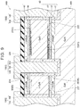
- the semiconductor device 1 A includes a substrate 10 Sub, semiconductor laminated body 6 , drain portion 1 D, source portion 1 S, and a plurality of gate portions 1 G.
- the substrate 10 Sub is formed of a material that permits crystal growth of the semiconductor laminated body 6 .
- the semiconductor laminated body 6 is a nitride semiconductor. Therefore, a semi-insulating substrate of a nitride semiconductor or silicon, for example, sapphire substrate, or the like, may be used as the substrate 10 Sub, though it is not particularly limited to these materials.
- the semiconductor laminated body 6 is a GaAs-based semiconductor, a GaAs-based semi-insulating substrate, sapphire substrate, or the like, may be used as the substrate 10 Sub, though it is not particularly limited to these materials.
- the substrate mentioned in this specification refers to a portion, having an interface level at its surface.
- the buffer layer forms a part of the semiconductor laminated body 6
- the substrate 10 Sub provides the substrate of this specification.
- the substrate 10 Sub including the buffer layer provides the substrate of this specification.
- the semiconductor laminated body 6 is provided on the surface of the substrate 10 Sub, and has a first semiconductor layer 1 , second semiconductor layer 2 , third semiconductor layer 3 , fourth semiconductor layer 4 , and fifth semiconductor layer 5 .
- the first semiconductor layer 1 , second semiconductor layer 2 , third semiconductor layer 3 , fourth semiconductor layer 4 , and fifth semiconductor layer 5 are laminated in this order on the surface of the substrate 10 Sub.
- the first semiconductor layer 1 , third semiconductor layer 3 , and fifth semiconductor layer 5 are i-AlGaN layers.
- the second semiconductor layer 2 and the fourth semiconductor layer 4 are i-GaN layers.
- the bandgap of i-AlGaN is wider than that of i-GaN. Therefore, the semiconductor laminated body 6 is constructed by joining adjacent semiconductor layers in the lamination direction to form heterojunctions.
- the i-AlGaN of the first semiconductor layer 1 , third semiconductor layer 3 and fifth semiconductor layer 5 is polarized through spontaneous polarization, and piezoelectric polarization.
- the first semiconductor layer 1 has negative fixed charge in the vicinity of its heterojunction interface with the second semiconductor layer 2 . Therefore, a two-dimensional hole gas layer (2DHG) is produced on the second semiconductor layer 2 side of the heterojunction interface between the first semiconductor layer 1 and the second semiconductor layer 2 .
- the third semiconductor layer 3 has positive fixed charge in the vicinity of its heterojunction interface with the second semiconductor layer 2 , and has negative fixed charge in the vicinity of its heterojunction interface with the fourth semiconductor layer 4 .
- a two-dimensional electron gas layer (2DEG) is produced on the second semiconductor layer 2 side of the heterojunction interface between the second semiconductor layer 2 and the third semiconductor layer 3
- a two-dimensional hole gas layer is produced on the fourth semiconductor layer 4 side of the heterojunction interface between the third semiconductor layer 3 and the fourth semiconductor layer 4
- the fifth semiconductor layer 5 has positive fixed charge in the vicinity of its heterojunction interface with the fourth semiconductor layer 4 . Therefore, a two-dimensional electron gas layer is produced on the fourth semiconductor layer 4 side of the heterojunction interface between the fourth semiconductor layer 4 and the fifth semiconductor layer 5 .
- two pairs of two-dimensional electron gas layer and two-dimensional hole gas layer are arranged in parallel rows in the lamination direction (Z direction). The two-dimensional electron gas layer and two-dimensional hole gas layer of each pair are opposed to each other in the lamination direction (Z direction).
- the drain portion 1 D and the source portion 1 S are spaced from each other in one direction (X direction), in a major plane of the semiconductor laminated body 6 .
- the drain portion 1 D is provided in a trench TR 1 for drain, which is formed through the semiconductor laminated body 6 to extend from a surface of the semiconductor laminated body 6 and reach the substrate 10 Sub.
- the dram portion 1 D may not reach the substrate 10 Sub, but is only required to extend through the two-dimensional electron gas layers and the two-dimensional hole gas layers.
- the source portion 1 S is provided in a trench TR 2 for source, which is formed through the semiconductor laminated body 6 to extend from the surface of the semiconductor laminated body 6 and reach the substrate 10 Sub.
- the source portion 1 S may not reach the substrate 10 Sub, but is only required to extend through the two-dimensional electron gas layers and the two-dimensional hole gas layers.
- Each of the gate portions 1 G is located between the drain portion 1 D and the source portion 1 S, and is provided in a trench TR 3 for gate, which is formed through the semiconductor laminated body 6 to extend from the surface of the semiconductor laminated body 6 and reach the substrate 10 Sub.
- each of the gate portions 1 G may not reach the substrate 10 Sub, but is only required to extend through the two-dimensional electron gas layers and the two-dimensional hole gas layers.
- the gate portions 1 G are arranged to be spaced from each other in a direction (Y direction) perpendicular to the direction (X direction) that connects the drain portion 1 D with the source portion 1 S, and the lamination direction (Z direction) of the semiconductor laminated body 6 .
- a part of the semiconductor laminated body 6 is provided between adjacent ones of the gate portions 1 G (see FIG. 2 ).
- the gate portions 1 G may be arranged along a straight line in the Y direction, or may be arranged while being slightly shifted in the X direction.
- a distance L 1 between adjacent ones of the gate portions 1 G may differ depending on the combination of adjacent gate portions 1 G.
- the gate portions 1 G are regularly arranged along the straight line in the Y direction.
- the distance L 1 between adjacent ones of the gate portions 1 G is constant or equal with respect to all combinations of adjacent gate portions 1 G While a plurality of gate portions 1 G is provided in this embodiment, it suffices that at least one gate portion 1 G is provided.
- Each of the drain portion 1 D and the source portion 1 S has an n-type semiconductor region.
- the n-type semiconductor region, of the drain portion 1 D may be arranged to fill the trench TR 1 for drain, or may be provided so as to cover the periphery of a metal electrode that fills the trench TR 1 for drain.
- the n-type semiconductor region of the source portion 1 S may also be arranged to fill the trench TR 2 for source, or may be provided so as to cover the periphery of a metal electrode that fills the trench TR 2 for source.
- each of the drain portion 1 D and the source portion 1 S has the n-type semiconductor region located at its surface in contact with the semiconductor laminated body 6 .
- Each of the gate portions 1 G has a p-type semiconductor region.
- the p-type semiconductor region of each of the gate portions 1 G may be arranged to fill the trench TR 3 for gate, or may be provided so as to cover the periphery of a metal electrode that fills the trench TR 3 for gate. In either case, each of the gate portions 1 G has the p-type semiconductor region located at its surface in contact with the semiconductor laminated body 6 .
- each of the drain portion 1 D and the source portion 1 S has then-type semiconductor region located at its surface in contact with the semiconductor laminated body 6 . Therefore, the n-type semiconductor region of each of the drain portion 1 D and the source portion 1 S is electrically connected to, typically, in ohmic contact with the two-dimensional electron gas layers (2DEG) produced in the semiconductor laminated body 6 . On the other hand, the n-type semiconductor region of each of the drain portion 1 D and the source portion 1 S is electrically insulated from the two-dimensional hole gas layers (2DEG) produced in the semiconductor laminated body 6 .
- the n-type semiconductor region of the drain portion 1 D may be electrically insulated from the two-dimensional hole gas layers produced in the semiconductor laminated body 6 , by contacting the hole gas layers via p-n junctions. However, the n-type semiconductor region of the drain portion 1 D is prevented by insulating regions 7 from contacting the two-dimensional hole gas layers via p-n junctions, so as to reduce the strength of electric field. More specifically, the n-type semiconductor region of the drain portion 1 D may be spaced from the two-dimensional hole gas layers by the insulating regions 7 , so as not to directly contact the two-dimensional hole gas layers.
- the insulating region 7 is a structure for eliminating a two-dimensional hole gas layer that would be produced in the absence of the insulating region 7 .
- the insulating region 7 may be present in a region between, each two-dimensional hole gas layer and the drain portion 1 D so as to eliminate the two-dimensional hole gas layer, or may be located adjacent to a region between each two-dimensional hole gas layer and the drain portion 1 D so as to eliminate the two-dimensional hole gas layer.
- the insulating region 7 is in the form of, for example, a void, insulating body, or insulating or semi-insulating high-resistance semiconductor.
- the n-type semiconductor region of the source portion 1 S may be electrically insulated from the two-dimensional hole gas layers produced in the semiconductor laminated body 6 , by contacting the hole gas layers via p-n junctions. However, the n-type semiconductor region of the source portion 1 S is prevented by insulating regions 8 from contacting the two-dimensional hole gas layers via p-n junctions, so as to reduce the strength of electric field. More specifically, the n-type semiconductor region of the source portion 1 S may be spaced from the two-dimensional hole gas layers by the insulating regions 8 , so as not to directly contact the two-dimensional hole gas layers.
- the insulating region 8 is a structure for eliminating a two-dimensional hole gas layer that would be produced in the absence of the insulating region 8 .
- the insulating region 8 may be present in a region between each two-dimensional hole gas layer and the source portion 1 S so as to eliminate the two-dimensional hole gas layer, or may be located adjacent to a region between each two-dimensional hole gas layer and the source portion 1 S so as to eliminate the two-dimensional hole gas layer.
- the insulating region 8 is in the form of, for example, a void, insulating body, or insulating or semi-insulating high-resistance semiconductor.
- each of the gate portions 1 G has the p-type semiconductor region located at its surface in contact with the semiconductor laminated body 6 .
- the p-type semiconductor region of each of the gate portions 1 G is in ohmic contact with the two-dimensional hole gas layers produced in the semiconductor laminated body 6 .
- the p-type semiconductor region of each of the gate portions 1 G is electrically insulated from the two-dimensional electron gas layers produced in the semiconductor laminated body 6 .
- the p-type semiconductor region of each of the gate portions 1 G is prevented by insulating regions 9 from contacting the two-dimensional electron gas layers via p-n junctions.
- the p-type semiconductor region of each of the gate portions 1 G is spaced from the two-dimensional electron gas layers by the insulating regions 9 , so as not to directly contact the two-dimensional electron gas layers.
- the insulating region 9 is a structure for eliminating a two-dimensional electron gas layer that would be produced in the absence of the insulating region 9 .
- the insulating region 9 may be present in a region between each two-dimensional electron gas layer and the gate portion 1 C so as to eliminate the two-dimensional electron gas layer, or may be located adjacent to a region between each two-dimensional electron gas layer and the gate portion 1 C so as to eliminate the two-dimensional electron gas layer.
- the insulating region 9 is in the form of, for example, a void, insulating body, or insulating or semi-insulating high-resistance semiconductor.
- the semiconductor device 1 A When a positive voltage is applied to the drain portion 1 D, and the source portion 1 S is grounded, while the gate portions 1 G are grounded, the semiconductor device 1 A is placed in the ON state. At this time, the drain portion 1 D and the source portion 1 S are electrically connected to each other, via the two-dimensional electron gas layers in the semiconductor laminated body 6 . Thus, the semiconductor device 1 A can provide low ON resistance, since electric current flows via the two-dimensional electron gas layers.
- the semiconductor device 1 A When a positive voltage is applied to the drain portion 1 D, and the source portion 1 S is grounded, while a negative voltage is applied to each gate portion 1 G, the semiconductor device 1 A is placed in the OFF state.
- the gate portion 1 G is in ohmic contact with the two-dimensional hole gas layers in the semiconductor laminated body 6 . Therefore, the potential of the two-dimensional hole gas layers in the semiconductor laminated body 6 can vary in accordance with the potential applied to the gate portion 1 G.
- a negative voltage is applied to the gate portion 1 G, so that a negative voltage is applied to the two-dimensional hole gas layers in the semiconductor laminated body 6 .
- the two-dimensional hole gas layers and two-dimensional electron gas layers in the semiconductor laminated body 6 are depleted.
- the semiconductor device 1 A has a heterojunction type superjunction structure, and can make the strength of electric field between the drain portion 1 D and the source portion 1 S uniform, like a superjunction structure of a normal p-n junction type.
- the strength of electric field in a drift region between the drain portion 1 D and the gate portion 1 G can be made uniform, so that the semiconductor device 1 A can exhibit a high breakdown voltage characteristic.
- the p-type semiconductor region of each of the gate portions 1 G is insulated by the insulating regions 9 , from the two-dimensional electron gas layers in the semiconductor laminated body 6 . Therefore, a sufficiently low negative voltage can be applied to the p-type semiconductor region of each of the gate portions 1 G, while curbing insulation leakage between the p-type semiconductor region of each of the gate portions 1 G and the two-dimensional electron gas layers.
- the insulating region 9 is configured to maintain its insulating performance at a threshold voltage applied to the gate portion 1 G.
- the n-type semiconductor region of each of the drain portion 1 D and the source portion 1 S is insulated by the insulating regions 7 , 8 , from the two-dimensional hole gas layers in the semiconductor laminated body 6 . Therefore, insulation leakage is less likely or unlikely to occur between the n-type semiconductor region of each of the drain portion 1 D and the source portion 1 S and the two-dimensional hole gas layers, and the semiconductor device 1 A can exhibit a high breakdown voltage characteristic.
- an electric field formed in the fifth semiconductor layer 5 is weaker than those of the other semiconductor layers 2 , 3 , 4 , due to an influence of its surface level.
- the semiconductor device 1 A when the semiconductor device 1 A is placed in the OFF state, carriers caused by background impurities (impurities un intendedly contained during manufacture) in the first semiconductor layer 1 and the fifth semiconductor layer 5 remain, and there is a concern that the first semiconductor layer 1 and the fifth semiconductor layer 5 may not be completely depleted.
- the thickness T 1 of the first semiconductor layer 1 and the thickness T 5 of the fifth semiconductor layer 5 are adjusted, so as to increase the strength of the electric field formed in the first semiconductor layer 1 and the strength of the electric field formed in the fifth semiconductor layer 5 .
- the electric field applied to the first semiconductor layer 1 is based on a potential difference arising from the two-dimensional hole gas layer immediately above the first semiconductor layer 1 and the interface level. Therefore, the strength of the electric field applied to the first semiconductor layer 1 is increased by reducing the thickness T 1 of the first semiconductor layer.
- the electric field applied to the fifth semiconductor layer 5 is based on a potential difference arising from the two-dimensional electron gas layer immediately below the fifth semiconductor layer 5 and the surface level.
- the thickness T 1 of the first semiconductor layer 1 and the thickness T 5 of the fifth semiconductor layer 5 may be adjusted so as to be smaller than any of the distances between adjacent ones of the two-dimensional electron gas layers and two-dimensional hole gas layers in the semiconductor laminated body 6 .
- the thickness T 1 of the first semiconductor layer 1 and the thickness T 5 of the fifth semiconductor layer 5 may be smaller than the thicknesses T 2 , T 3 , T 4 of the other semiconductor layers 2 , 3 , 4 .
- the thicknesses T 2 , T 3 , T 4 of the semiconductor layers 2 , 3 , 4 are equal.
- the thickness T 1 of the first semiconductor layer 1 and the thickness T 5 of the fifth semiconductor layer 5 thus adjusted, the carriers derived from the background impurities in the first semiconductor layer 1 and the fifth semiconductor layer 5 are removed and the first semiconductor layer 1 and the fifth semiconductor layer 5 are favorably depleted.
- the interface level is formed between the first semiconductor layer 1 and the substrate 10 Sub, and the surface level is formed on the surface of the fifth semiconductor layer 5 .
- the interface level and the surface level are not stabilized for various reasons, and may become lower levels than expected. Therefore, there is a concern that the first semiconductor layer 1 and the fifth semiconductor layer 5 may not be favorably depleted, even if the thickness T 1 of the first semiconductor layer 1 and the thickness T 5 of the fifth semiconductor layer 5 are adjusted to be small.
- defects may be introduced into the interface between the first semiconductor layer 1 , and the substrate 10 Sub so that the interface defect density becomes equal to or greater than 1 ⁇ 10 11 cm ⁇ 2 , and defects may be introduced into the surface or interface of the fifth semiconductor layer 5 so that the surface defect density of the fifth semiconductor layer 5 becomes equal to or greater than 1 ⁇ 10 11 cm ⁇ 2 .
- the effects of the interface level and the surface level are sufficiently yielded, and the first semiconductor layer 1 and the fifth semiconductor layer 5 can be favorably depleted when the thickness T 1 of the first semiconductor layer 1 and the thickness T 5 of the fifth semiconductor layer 5 are adjusted to be small.
- the carrier density of a carrier gas layer in this example, 2DHG in the vicinity of the heterojunction interface between the first semiconductor layer 1 and the second semiconductor layer 2
- the carrier density of a carrier gas layer in this example, 2DEG in the vicinity of the hetero junction interface between the fourth semiconductor layer 4 and the fifth semiconductor layer 5
- the carrier densities of the other two-dimensional electron gas layer and two-dimensional hole gas layer become larger than the carrier densities of the other two-dimensional electron gas layer and two-dimensional hole gas layer.
- the carrier balance of the two-dimensional electron gas layers and the two-dimensional hole gas layers is impaired or lost.
- the semiconductor device 1 A when the semiconductor device 1 A is placed in the OFF state, carriers corresponding to the difference in the carrier density may remain, and the semiconductor laminated body 6 may not be favorably depleted.
- the thickness T 1 of the first semiconductor layer 1 is adjusted to be small, the carrier density of the carrier gas layer closest to the rear surface of the semiconductor laminated body 6 is reduced. If the thickness T 5 of the fifth semiconductor layer 5 is adjusted to be small, the carrier density of the carrier gas layer closest to the top face of the semiconductor laminated body 6 is reduced.
- the carrier densities of all of the two-dimensional electron gas layers and two-dimensional hole gas layers in the semiconductor laminated body 6 become substantially equal.
- the semiconductor laminated body 6 is favorably depleted, and the semiconductor device 1 A has a high breakdown voltage characteristic.
- the carrier densities of two carrier gas layers are substantially equal to each other, when a difference between the carrier densities is equal to or smaller than 10%. It is desirable that the difference between the carrier densities of two carrier gas layers is equal to or smaller than 5%.
- the semiconductor laminated body 6 can be favorably depleted. Namely, in the case of this embodiment, it suffices that a pair of the 2DHG in the vicinity of the heterojunction interface of the first semiconductor layer 1 and the second semiconductor layer 2 , and the 2DEG in the vicinity of the heterojunction interface of the second semiconductor layer 2 and the third semiconductor layer 3 , have substantially the same carrier density.
- a pair of the 2DHG in the vicinity of the heterojunction interface of the third semiconductor layer 3 and the fourth semiconductor layer 4 , and the 2DEG in the vicinity of the heterojunction interface of the fourth semiconductor layer 4 and the fifth semiconductor layer 5 have substantially the same carrier density.
- the carrier density of the former pair may be equal to or different from the carrier density of the latter pair. Accordingly, it is also effective to adjust the thickness T 1 of the first semiconductor layer 1 and the thickness 15 of the fifth semiconductor layer 5 , so as to satisfy the above relationship. In this case, too, when the semiconductor device 1 A is placed in the OFF state, the semiconductor laminated body 6 is favorably depleted, so that the semiconductor device 1 A can exhibit a high breakdown voltage characteristic.
- the above arrangement may also be applied to an embodiment in which only one pair of a two-dimensional electron gas layer and a two-dimensional electron hole layer are present in the semiconductor device, and an embodiment in which three or more pairs of two-dimensional electron gas layers and two-dimensional hole gas layers are present in the semiconductor device.
- L 1 denotes the distance
- L 2 denotes the distance between the gate portion 1 G and the drain portion 1 D
- a relationship of L 1 ⁇ 2 ⁇ L 2 may be satisfied.
- the distance L 1 may be maximized as long as the relationship of L 1 ⁇ 2 ⁇ L 2 is satisfied. As a result, the distance L 1 between adjacent ones of the gate portions 1 G is increased, so that the channel resistance can be minimized.
- L 1 denotes the distance between adjacent ones of the gate portions 1 G
- W 1 denotes the width of the gate portion 10 as measured in the direction (X direction) that connects the drain portion 1 D with the source portion 1 S
- L 1 ⁇ W 1 may be satisfied. With this relationship satisfied, even when a high voltage is applied to the drain portion 1 D, because of shorting of a load, for example, portions between adjacent ones of the gate portions 1 G can be kept depleted. Thus, the semiconductor device 1 A can exhibit a high breakdown voltage characteristic.
- the semiconductor laminated body 6 may be configured such that the two-dimensional electron gas layer is located in a quantum well or in a superlattice structure. Also, the semiconductor laminated body 6 may be configured such that the two-dimensional hole gas layer is located in a quantum well or in a superlattice structure. In this connection, leak current can be reduced if either one of the two-dimensional electron gas layer and the two-dimensional hole gas layer is located in a quantum well or in a superlattice structure.
- FIG. 5 shows a semiconductor device 1 B of a second embodiment.
- the same reference numerals are assigned to substantially the same constituent elements as those of the semiconductor device 1 A of the first embodiment, and explanation of these elements may not be provided.
- a plurality of gate portions 2 G is arranged to be spaced from each other in a direction perpendicular to the direction that connects the drain portion 1 D with the source portion 1 S and the lamination direction of the semiconductor laminated body 6 , like the gate portions 1 G of FIG. 3 and FIG. 4 .
- the semiconductor device 1 B is characterized in that each of the gate portions 2 G has a Schottky electrode. In each of the gate portions 2 G, the trench TR 3 for gate is filled with the Schottky electrode.
- the Schottky electrode in each of the gate portions 2 G is electrically insulated from both of the two-dimensional electron gas layers (2DEG) and the two-dimensional hole gas layers (2DHG) produced in the semiconductor laminated body 6 .
- the Schottky electrode in each of the gate portions 2 G is prevented by insulating regions 9 a from contacting the two-dimensional electron gas layers via Schottky junction. More specifically, the Schottky electrode of each of the gate portions 2 G is spaced from the two-dimensional electron gas layers with the insulating regions 9 a provided therebetween, so that the Schottky electrode does not directly contact the two-dimensional electron gas layers.
- the insulating region 9 a is a structure for eliminating a two-dimensional electron gas layer that would be produced in the absence of the insulating region 9 a .
- the insulating region 9 a may be present in a region between each two-dimensional electron gas layer and the Schottky electrode of the gate portion 2 G so as to eliminate the two-dimensional electron gas layer, or may be located adjacent to a region between the two-dimensional electron gas layer and the Schottky electrode of the gate portion 2 G so as to eliminate the two-dimensional electron gas layer.
- the insulating region 9 a is in the form of for example, a void, insulating body, or insulating or semi-insulating high-resistance semiconductor.
- the Schottky electrode in each of the gate portions 2 G is prevented by insulating regions 9 b from contacting the two-dimensional hole gas layers via Schottky junction. More specifically, the Schottky electrode of each of the gate portions 2 G is spaced from the two-dimensional hole gas layers with the insulating regions 9 b provided therebetween, so that the Schottky electrode does not directly contact the two-dimensional hole gas layers.
- the insulating region 9 b is a structure for eliminating a two-dimensional hole gas layer that would be produced in the absence of the insulating region 9 b .
- the insulating region 9 b may be present in a region between each two-dimensional hole gas layer and the Schottky electrode of the gate portion 2 G so as to eliminate the two-dimensional hole gas layer, or may be located adjacent to a region between each two-dimensional hole gas layer and the Schottky electrode of the gate portion 2 G so as to eliminate the two-dimensional hole gas layer.
- the insulating region 9 b is in the form of, for example, a void, insulating body, or insulating or semi-insulating high-resistance semiconductor.
- each of the two-dimensional hole gas layers in the semiconductor laminated body 6 is insulated from all of the drain portion 1 D, source portion 1 S, and gate portions 2 G; therefore, the potential of the two-dimensional hole gas layer is in a floating state.
- capacitors provided by the insulating regions 9 b between the gate portions 2 G and the two-dimensional hole gas layers are connected in series with capacitors provided by the semiconductor layers 2 , 4 between the two-dimensional hole gas layers and the two-dimensional electron gas layers and the series-connected capacitors are present between the gate portion 2 G and the drain portion 1 D.
- voltage Vpn between the two-dimensional hole gas layer and the two-dimensional electron gas layer can be expressed by an equation below, where Cgp denotes the capacitance between the gate portion 2 G and the two-dimensional hole gas layer, Cpn denotes the capacitance between the two-dimensional hole gas layer and the two-dimensional electron gas layer, and Vgn denotes the voltage between the gate portion 2 G and the two-dimensional electron gas layer.
- Vpn Vgn ⁇ Cgp /( Cgp+Cpn )
- the potential of the two-dimensional hole gas layer in the semiconductor laminated body 6 can vary in accordance with the potential applied to the gate portion 2 G, through capacitance coupling.
- a negative voltage is applied to the gate portions 2 G
- a negative voltage is applied to the two-dimensional hole gas layers in the semiconductor laminated body 6 .
- the two-dimensional hole gas layers and two-dimensional electron gas layers in the semiconductor laminated body 6 are depleted.
- positive and negative fixed charges remain in the first semiconductor layer 1 , third semiconductor layer 3 , and fifth semiconductor layer 5 .
- the semiconductor device 1 B has a hetero junction type superjunction structure, and the strength of the electrode field between the drain portion 1 D and the gate portion 2 G can be made uniform, like a general p-n junction type superjunction structure. As a result, the semiconductor device 1 B can exhibit a high breakdown voltage characteristic.
- a semiconductor device 10 A includes a substrate 100 , semiconductor laminated body 10 , drain portion 100 D, source portion 100 S, and a plurality of gate portions 100 G.
- the gate portions 100 G are arranged to be spaced from each other in a direction perpendicular to the direction that connects the drain portion 100 D with the source region 100 S and the lamination direction of the semiconductor laminated body 10 , like the gate portions 1 G of FIG. 3 and FIG. 4 .
- the substrate 100 is a semi-insulating GaAs substrate.
- the substrate 100 may include a buffer layer of a GaAs-based semiconductor, for improvement of the crystalline nature of the semiconductor laminated body 10 .
- the semiconductor laminated body 10 is located between the drain portion 100 D and the source portion 100 S, and has a first barrier layer 11 of i-AlGaAs, hole supply layer 12 of p-InGaP, channel layer 13 of i-GaAs, electron supply layer 14 of n-InGaP, and second barrier layer 15 of i-AlGaAs.
- the first barrier layer 11 , hole supply layer 12 , channel layer 13 , electron supply layer 14 , and second barrier layer 15 are grown and formed in this order from a surface of the substrate 100 , by a metal organic chemical vapor deposition (MOCVD) method.
- MOCVD metal organic chemical vapor deposition
- a protective film of silicon oxide is formed by a chemical vapor deposition (CVD) method.
- the drain portion 100 D is formed through the semiconductor laminated body 10 to extend from the surface of the semiconductor laminated body 10 and reach the substrate 100 , and has a drain electrode 101 and an n-type drain semiconductor region 102 .
- the n-type drain semiconductor region 102 which is provided between the drain electrode 101 and the semiconductor laminated body 10 , covers the most part of a side face and a bottom of the drain electrode 101 , and is in contact with both the drain electrode 101 and the semiconductor laminated body 10 .
- the drain portion 100 D has the n-type drain semiconductor region 102 located on its surfaces in contact with the semiconductor laminated body 10 .
- the n-type drain semiconductor region 102 is formed by forming a trench for forming the drain portion 100 D, and then introducing n-type impurities into a side wall and a bottom of the trench, using an oblique ion implantation technique.
- Each of the gate portions 100 G is formed through the semiconductor laminated body 10 to extend from the surface of the semiconductor laminated body 10 and reach the substrate 100 , and has a gate electrode 103 and a p-type gate semiconductor region 104 .
- the p-type gate semiconductor region 104 which is provided between the gate electrode 103 and the semiconductor laminated body 10 , covers the most part of side faces and a bottom of the gate electrode 103 , and is in contact with both the gate electrode 103 and the semiconductor laminated body 10 .
- the gate portion 100 G has the p-type gate semiconductor region 104 located on its surfaces in contact with the semiconductor laminated body 10 .
- the p-type gate semiconductor region 104 is formed by forming a trench for forming the gate portion 100 G, and then introducing p-type impurities into side walls and bottom of the trench, using the oblique ion implantation technique.
- the source portion 100 S is formed through the semiconductor laminated body 10 to extend from the surface of the semiconductor laminated body 10 and reach the substrate 100 , and has a source electrode 105 and an n-type source semiconductor region 106 .
- the n-type source semiconductor region 106 which is provided between the source electrode 105 and the semiconductor laminated body 10 , covers the most part of a side face and a bottom of the source electrode 105 , and is in contact with both the source electrode 105 and the semiconductor laminated body 10 .
- the source portion 100 S has the n-type source semiconductor region 106 located on its surfaces in contact with the semiconductor laminated body 10 .
- the n-type source semiconductor region 106 is formed by forming a trench for forming the source portion 100 S, and then introducing n-type impurities into a side wall and a bottom of the trench, using the oblique ion implantation technique.
- the semiconductor device 10 A further includes a drain-side insulating region 202 , gate-side insulating regions 204 , and source-side insulating region 206 . These insulating regions 202 , 204 , 206 are in the form of voids.
- the drain-side insulating region 202 is formed by etching a part of the hole supply layer 12 and a part of the n-type drain semiconductor region 102 , and is formed between the hole supply layer 12 and the drain electrode 101 of the drain portion 100 D. With the drain-side insulating region 202 thus provided, no two-dimensional hole gas layer (2DHG) is produced in the channel layer 13 adjacent to the drain-side insulating region 202 , and p-n junction is not formed between the two-dimensional hole gas layer and the n-type drain semiconductor region 102 .
- the drain-side insulating region 202 may be replaced with another alternative means, provided that the two-dimensional hole gas layer and the n-type drain semiconductor region 102 do not directly contact with each other.
- an insulator, or an insulating or semi-insulating high-resistance semiconductor of a material that does not give rise to a two-dimensional hole gas layer may be formed in a region corresponding to the drain-side insulating region 202 .
- a void, insulator, or insulating or semi-insulating high-resistance semiconductor may be formed at a position between the two-dimensional hole gas layer and the n-type drain semiconductor region 102 .
- Each of the gate-side insulating regions 204 is formed by etching a part of the electron supply layer 14 and a part of the p-type gate semiconductor region 104 , and is formed between the electron supply layer 14 and the gate electrode 103 of the gate portion 100 G.
- the gate-side insulating region 204 thus provided, no two-dimensional electron gas layer is produced in the channel layer 13 adjacent to the gate-side insulating region 204 , and p-n junction is not formed between the two-dimensional electron gas layer and the p-type gate semiconductor region 104 .
- the gate-side insulating region 204 may be replaced with another alternative means, provided that the two-dimensional electron gas layer and the p-type gate semiconductor region 104 do not directly contact with each other.
- an insulator, or an insulating or semi-insulating high-resistance semiconductor of a material that does not give rise to a two-dimensional electron gas layer may be formed in a region corresponding to the gate-side insulating region 204 .
- a void, insulator, or insulating or semi-insulating high-resistance semiconductor may be formed at a position between the two-dimensional electron gas layer and the p-type gate semiconductor region 104 .
- the source-side insulating region 206 is formed by etching a part of the hole supply layer 12 and a part of the n-type source semiconductor region 106 , and is formed between the hole supply layer 12 and the source electrode 105 of the source portion 100 S. With the source-side insulating region 206 thus provided, no two-dimensional hole gas layer is produced in the channel layer 13 adjacent to the source-side insulating region 206 , and p-n junction is not formed between the two-dimensional hole gas layer and the n-type source semiconductor region 106 .
- the source-side insulating region 206 may be replaced with another alternative means, provided that the two-dimensional hole gas layer and the n-type source semiconductor region 106 do not directly contact with each other.
- an insulator, or an insulating or semi-insulating high-resistance semiconductor of a material that does not give rise to a two-dimensional hole gas layer may be formed in a region corresponding to the source-side insulating region 206 .
- a void, insulator, or insulating or semi-insulating high-resistance semiconductor may be formed at a position between the two-dimensional hole gas layer and the n-type source semiconductor region 106 .
- the drain-side insulating region 202 , gate-side insulating regions 204 , and source-side insulating region 206 may be formed through the following process. Initially, trenches that extend from the surface of the semiconductor laminated body 10 through the second barrier layer 15 and reach the electron supply layer 14 are formed, as parts of the trenches for forming the drain portion 100 D, gate portions 100 G, and source portion 100 S, using an etchant A (e.g., a mixture of sulfuric acid and hydrogen peroxide solution) with which GaAs and AlGaAs can be etched.
- an etchant A e.g., a mixture of sulfuric acid and hydrogen peroxide solution
- the electron supply layer 14 is selectively etched, using an etchant B (e.g., hydrochloric acid) having a higher etching rate for InGaP than for GaAs and AlGaAs, to thus form the gate-side insulating regions 204 .
- etchant B e.g., hydrochloric acid
- the lateral width of each gate-side insulating region 204 is several ⁇ m.
- the hole supply layer 12 is selectively etched, using the etchant B, so that the drain-side insulating region 202 and the source-side insulating region 206 are formed.
- the lateral width of each of the drain-side insulating region 202 and the source-side insulating region 206 is several ⁇ m. In this manner, in the process of forming the drain portion 100 D, gate portions 100 G, and source portion 100 S, the drain-side insulating region 202 , gate-side insulating regions 204 , and source-side insulating region 206 can be formed.
- the drain portion 100 D gate portions 100 G, and source portion 100 S may be further formed through the next process.
- the trenches are made even deeper so as to extend through the first barrier layer 11 and reach the substrate 100 .
- the drain electrode 101 , gate electrodes 103 , and source electrode 105 are formed in the trenches, by a sputtering method or a vapor deposition method.
- the semiconductor device 10 A When a positive voltage is applied to the drain electrode 101 of the drain portion 100 D, and the source electrode 105 of the source portion 100 S is grounded, while the gate electrodes 103 of the gate portions 100 G are grounded, the semiconductor device 10 A is placed in the ON state. At this time, holes are supplied from the hole supply layer 12 , to the channel layer 13 side of the heterojunction interface between the hole supply layer 12 and the channel layer 13 , to form a two-dimensional hole gas layer. On the other hand, electrons are supplied from the electron supply layer 14 , to the channel layer 13 side of the heterojunction interface between the channel layer 13 and the electron supply layer 14 , to form a two-dimensional electron gas layer.
- the drain portion 100 D and the source portion 100 S are electrically connected with each other via the two-dimensional electron gas layer in the semiconductor laminated body 10 .
- the semiconductor device 10 A can provide low ON-resistance, since current flows through the two-dimensional electron gas layer.
- the semiconductor device 10 A When a positive voltage is applied to the drain electrode 101 of the drain portion 100 D, and the source electrode 105 of the source portion 100 S is grounded, while a negative voltage is applied to the gate electrode 103 of each gate portion 100 G the semiconductor device 10 A is placed in the OFF state.
- the p-type gate semiconductor region 104 of each of the gate portions 100 G is in ohmic contact with the two-dimensional hole gas layer in the semiconductor laminated body 10 . Therefore, the potential of the two-dimensional hole gas layer in the semiconductor laminated body 10 can vary in accordance with the potential applied to the gate electrode 103 of the gate portion 100 G. In this case, since a negative voltage is applied to the gate portion 100 G, a negative voltage is applied to the two-dimensional hole gas layer in the semiconductor laminated body 10 .
- the semiconductor device 10 A has the heterojunction type superjunction structure, and the strength of the electric field between the drain portion 100 D and the source portion 100 S can be made uniform. In particular, the strength of electric field in a drift region between the drain portion 100 D and the gate portion 100 G can be made uniform, so that the semiconductor device 10 A can exhibit a high breakdown voltage characteristic.
- the p-type gate semiconductor region 104 of each gate portion 100 G is insulated by the gate-side insulating region 204 , from the two-dimensional electron gas layer in the semiconductor laminated body 10 . Therefore, it is possible to apply a sufficiently low voltage to the gate electrode 103 of the gate portion 100 G, while curbing insulation leakage between the p-type gate semiconductor region 104 of the gate portion 100 G and the two-dimensional electron gas layer.
- the two-dimensional hole gas layer and two-dimensional electron gas layer in the semiconductor laminated body 10 are favorably depleted, and the semiconductor device 10 A can exhibit a high breakdown voltage characteristic.
- the n-type drain semiconductor region 102 of the drain portion 100 D is insulated by the drain-side insulating region 202 from the two-dimensional hole gas layer in the semiconductor laminated body 10
- the n-type source semiconductor region 106 of the source portion 100 S is insulated by the source-side insulating region 206 from the two-dimensional hole gas layer in the semiconductor laminated body 10 . Therefore, insulation leakage is less likely or unlikely to occur between the n-type drain semiconductor region 102 of the drain portion 100 D and the two-dimensional hole gas layer, and between the n-type source semiconductor region 106 of the source portion 100 S and the two-dimensional hole gas layer, and the semiconductor device 10 A can exhibit a high breakdown voltage characteristic.
- the thickness of the first barrier layer 11 and the thickness of the second barrier layer 15 are adjusted to be smaller than the distance between the two-dimensional electron gas layer and the two-dimensional hole gas layer.
- FIG. 7 shows a semiconductor device 10 B of a second embodiment.
- the semiconductor device 10 B includes a substrate 200 , semiconductor laminated body 20 , drain portion 100 D, source portion 100 S, and a plurality of gate portions 100 G.
- the gate portions 100 G are arranged to be spaced from each other in a direction perpendicular to the direction that connects the drain portion 100 D with the source region 100 S and the lamination direction of the semiconductor laminated body 20 , like the gate portions 1 G of FIG. 3 and FIG. 4 .
- the substrate 200 is a semi-insulating GaAs substrate.
- the substrate 200 may include a buffer layer of a GaAs-based semiconductor, for improvement of the crystalline nature of the semiconductor laminated body 20 .
- the semiconductor laminated body 20 is located between the drain portion 100 D and the source portion 100 S, and has a first barrier layer 21 of i-AlGaAs, p-channel quantum well layer 22 of i-GaAs, hole supply layer 23 of i-InGaP, channel layer 24 of i-GaAs, electron supply layer 25 of i-InGaP, n-channel quantum well layer 26 of i-GaAs, and second barrier layer 27 of i-AlGaAs.
- a p-type ⁇ doped layer containing p-type impurities is formed at a position adjacent to the p-channel quantum well layer 22 .
- an n-type ⁇ doped layer containing n-type impurities is formed at a position adjacent to the n-channel quantum well layer 26 .
- the first barrier layer 21 , p-channel quantum well layer 22 , hole supply layer 23 , channel layer 24 , electron supply layer 25 , n-channel quantum well layer 26 , and second barrier layer 27 are grown and formed in this order from a surface of the substrate 200 , by the metal organic chemical vapor deposition method.
- the semiconductor device 10 B further includes a drain-side insulating region 210 , gate-side insulating regions 212 , and a source-side insulating region 214 . These insulating regions 210 , 212 , 214 are in the for of voids.
- the drain-side insulating region 210 is formed by etching a part of the hole supply layer 23 and a part of the n-type drain semiconductor region 102 , and is formed between the hole supply layer 23 and the drain electrode 101 of the drain portion 100 D. With the drain-side insulating region 210 thus provided, no two-dimensional hole gas layer (2DHG) is produced in the p-channel quantum well layer 22 adjacent to the drain-side insulating region 210 , and p-n junction is not formed between the two-dimensional hole gas layer and the n-type drain semiconductor region 102 .
- the drain-side insulating region 210 may be replaced with another alternative means, provided that the two-dimensional hole gas layer and the n-type drain semiconductor region 102 do not directly contact with each other.
- an insulator, or an insulating or semi-insulating high-resistance semiconductor of a material that does not give rise to a two-dimensional hole gas layer may be formed in a region corresponding to the drain-side insulating region 210 .
- a void, insulator, or insulating or semi-insulating high-resistance semiconductor may be formed at a position between the two-dimensional hole gas layer and the n-type drain semiconductor region 102 .
- Each of the gate-side insulating regions 212 is formed by etching a part of the electron supply layer 25 and a part of the p-type gate semiconductor region 104 , and is formed between the electron supply layer 25 and the gate electrode 103 of the gate portion 100 G.
- the gate-side insulating region 212 thus provided, no two-dimensional electron gas layer is produced in the n-channel quantum well layer 26 adjacent to the gate-side insulating region 212 , and p-n junction is not formed between the two-dimensional electron gas layer and the p-type gate semiconductor region 104 .
- the gate-side insulating region 212 may be replaced with another alternative means, provided that the two-dimensional electron gas layer and the p-type gate semiconductor region 104 do not directly contact with each other.
- an insulator, or an insulating or semi-insulating high-resistance semiconductor of a material that does not give rise to a two-dimensional electron gas layer may be formed in a region corresponding to the gate-side insulating region 212 .
- a void, insulator, or insulating or semi-insulating high-resistance semiconductor may be formed at a position between the two-dimensional electron gas layer and the p-type gate semiconductor region 104 .
- the source-side insulating region 214 is formed by etching a part of the hole supply layer 23 and a part of the n-type source semiconductor region 106 , and is formed between the hole supply layer 23 and the source electrode 105 of the source portion 100 S. With the source-side insulating region 214 thus provided, no two-dimensional hole gas layer is produced in the p-channel quantum well layer 22 adjacent to the source-side insulating region 214 , and p-n junction is not formed between the two-dimensional hole gas layer and the n-type source semiconductor region 106 .
- the source-side insulating region 214 may be replaced with another alternative means, provided that the two-dimensional hole gas layer and the n-type source semiconductor region 106 do not directly contact with each other.
- an insulator, or an insulating or semi-insulating high-resistance semiconductor of a material that does not give rise to a two-dimensional hole gas layer may be formed in a region corresponding to the source-side insulating region 214 .
- a void, insulator, or insulating or semi-insulating high-resistance semiconductor may be formed at a position between the two-dimensional hole gas layer and the n-type source semiconductor region 106 .
- the drain-side insulating region 210 , gate-side insulating regions 212 , and source-side insulating region 214 may be formed through the following process. Initially, trenches that extend from the surface of the semiconductor laminated body 20 through the second barrier layer 27 and the n-channel quantum well layer 26 and reach the electron supply layer 25 are formed, as parts of the trenches for forming the drain portion 100 D, gate portions 100 G, and source portion 100 S, using an etchant A (e.g., a mixture of sulfuric acid and hydrogen peroxide solution) with which GaAs and AlGaAs can be etched.
- an etchant A e.g., a mixture of sulfuric acid and hydrogen peroxide solution
- the electron supply layer 25 is selectively etched, using an etchant B (e.g., hydrochloric acid) having a higher etching rate for InGaP than for GaAs and AlGaAs, to thus form the gate-side insulating regions 212 .
- etchant B e.g., hydrochloric acid
- the lateral width of the gate side insulating region 212 is several ⁇ m.
- the hole supply layer 23 is selectively etched, using the etchant B, so that the drain-side insulating region 210 and the source-side insulating region 214 are formed.
- the lateral width of each of the drain-side insulating region 210 and the source-side insulating region 214 is several ⁇ m. In this manner, in the process of forming the drain portion 100 D, gate portions 100 G, and source portion 100 S, the drain-side insulating region 210 , gate-side insulating regions 212 , and source-side insulating region 214 can be formed.
- the drain portion 100 D, gate portions 100 G, and source portion 100 S may be further formed through the next process.
- the trenches are made even deeper so as to extend through the p-channel quantum well layer 22 and first barrier 21 and reach the substrate 200 , using the etchant A. Then, after the n-type drain, semiconductor region 102 , p-type gate semiconductor regions 104 , and n-type source semiconductor region 106 are formed, using the oblique ion implantation technique, as described above, the drain electrode 101 , gate electrodes 103 , and source electrode 105 are formed in the trenches, by the sputtering method or vapor deposition method.
- the semiconductor device 10 B When a positive voltage is applied to the drain electrode 101 of the drain portion 100 D, and the source electrode 105 of the source portion 100 S is grounded, while the gate electrodes 103 of the gate portions 100 G are grounded, the semiconductor device 10 B is placed in the ON state. At this time, holes are supplied from the p-type ⁇ doped layer of the hole supply layer 23 , to the p-channel quantum well layer 22 side of the heterojunction interface between the p-channel quantum well layer 22 and the hole supply layer 23 , to form a two-dimensional hole gas layer.
- the semiconductor device 10 B can provide low ON-resistance, since current flows through the two-dimensional electron gas layer.
- the semiconductor device 10 B When a positive voltage is applied to the drain electrode 101 of the drain portion 100 D, and the source electrode 105 of the source portion 100 S is grounded, while a negative voltage is applied to the gate electrode 103 of each gate portion 100 G, the semiconductor device 10 B is placed in the OFF state.
- the p-type gate semiconductor region 104 of each of the gate portions 100 G is in ohmic contact with the two-dimensional hole gas layer in the semiconductor laminated body 20 . Therefore, the potential of the two-dimensional hole gas layer in the semiconductor laminated body 20 can vary in accordance with the potential applied to the gate electrodes 103 of the gate portions 100 G. In this case, since a negative voltage is applied to the gate portion 100 G, a negative voltage is applied to the two-dimensional hole gas layer in the semiconductor laminated body 20 .
- the semiconductor device 10 B has a heterojunction type superjunction structure, and the strength of the electric field between the drain portion 100 D and the source portion 100 S can be made uniform. In particular, the strength of the electric field in a drift region between the drain portion 100 D and the gate portion 100 G can be made uniform, so that the semiconductor device 10 B can exhibit a high breakdown voltage characteristic.
- the p-type gate semiconductor region 104 of each gate portion 100 G is insulated by the gate-side insulating region 212 , from the two-dimensional electron gas layer in the semiconductor laminated body 20 . Therefore, it is possible to apply a sufficiently low voltage to the gate electrode 103 of the gate portion 100 G, while curbing insulation leakage between the p-type gate semiconductor region 104 of the gate portion 100 G and the two-dimensional electron gas layer.
- the two-dimensional hole gas layer and two-dimensional electron gas layer in the semiconductor laminated body 20 are favorably depleted, and the semiconductor device 10 B can exhibit a high breakdown voltage characteristic.
- the n-type drain semiconductor region 102 of the drain portion 100 D is insulated by the drain-side insulating region 210 , from the two-dimensional hole gas layer in the semiconductor laminated body 20 , and the n-type source semiconductor region 106 of the source portion 100 S is insulated by the source-side insulating region 214 from the two-dimensional hole gas layer in the semiconductor laminated body 20 . Therefore, insulation leakage is less likely or unlikely to occur between the n-type drain semiconductor region 102 of the drain portion 100 D and the two-dimensional hole gas layer, and between the n-type source semiconductor region 106 of the source portion 100 S and the two-dimensional hole gas layer, and the semiconductor device 10 B can exhibit a high breakdown voltage characteristic.
- the thickness of the first barrier layer 21 and the thickness of the second barrier layer 27 are adjusted to be smaller than the distance between the two-dimensional electron gas layer and the two-dimensional hole gas layer.
- the semiconductor device 10 B is configured such that both of the two-dimensional electron gas layer and the two-dimensional hole gas layer are produced in the quantum wells. Therefore, carriers are less likely or unlikely to leak from the quantum wells, and the semiconductor device 10 B can exhibit a low leakage current characteristic.
- FIG. 8 shows a semiconductor device 10 C of a third embodiment.
- the semiconductor device 10 C includes a substrate 300 , semiconductor laminated body 30 , drain portion 100 D, source portion 100 S, and a plurality of gate portions 100 G.
- the gate portions 100 G are arranged to be spaced from each other in a direction perpendicular to the direction that connects the drain portion 100 D with the source region 100 S and the lamination direction of the semiconductor laminated body 30 , like the gate portions 1 G of FIG. 3 and FIG. 4 .
- the substrate 300 is a semi-insulating GaAs substrate.
- the substrate 300 may include a buffer layer of a GaAs-based semiconductor, for improvement of the crystalline nature of the semiconductor laminated body 30 .
- the semiconductor laminated body 30 is located between the drain portion 100 D and the source portion 100 S, and has a first barrier layer 31 of i-AlGaAs, hole supply layer 32 of i-InGaP, channel layer 33 of i-GaAs, electron supply layer 34 of i-InGaP, and second barrier layer 35 of i-AlGaAs.
- a p-type ⁇ doped layer containing p-type impurities is formed at a position adjacent to the hole supply layer 32
- n-type ⁇ doped layer containing n-type impurities is formed at a position adjacent to the electron supply layer 34 .
- the first barrier layer 31 , hole supply layer 32 , channel layer 33 , electron supply layer 34 , and second barrier layer 35 are grown and formed in this order from a surface of the substrate 300 , by the metal organic chemical vapor deposition method.
- the semiconductor device 10 C further includes a drain-side insulating region 216 , gate-side insulating regions 218 , and source-side insulating region 220 . These insulating regions 216 , 218 , 220 are in the form of voids.
- the drain-side insulating region 216 is formed by etching a part of the hole supply layer 32 and a part of the n-type drain semiconductor region 102 , and is formed between the hole supply layer 32 and the drain electrode 101 of the drain portion 100 D. With the drain-side insulating region 216 thus provided, no two-dimensional hole gas layer (2DHG) is produced in the channel layer 33 adjacent to the drain-side insulating region 216 , and p-n junction is not formed between the two-dimensional hole gas layer and the n-type drain semiconductor region 102 .
- the drain-side insulating region 216 may be replaced with another alternative means, provided that the two-dimensional hole gas layer and the n-type drain semiconductor region 102 do not directly contact with each other.
- an insulator, or an insulating or semi-insulating high-resistance semiconductor of a material that does not give rise to a two-dimensional hole gas layer may be formed in a region corresponding to the drain-side insulating region 216 .
- a void, insulator, or insulating or semi-insulating high-resistance semiconductor may be formed at a position between the two-dimensional hole gas layer and the n-type drain semiconductor region 102 .
- Each of the gate-side insulating regions 218 is formed by etching a part of the electron supply layer 34 and a part of the p-type gate semiconductor region 104 , and is formed between the electron supply layer 34 and the gate electrode 103 of the gate portion 100 G.
- the gate-side insulating region 218 thus provided, no two-dimensional electron gas layer (2DEG) is produced in the channel layer 33 adjacent to the gate-side insulating region 218 , and p-n junction is not formed between the two-dimensional electron gas layer and the p-type gate semiconductor region 104 .
- the gate-side insulating region 218 may be replaced with another alternative means, provided that the two-dimensional electron gas layer and the p-type gate semiconductor region 104 do not directly contact with each other.
- an insulator, or an insulating or semi-insulating high-resistance semiconductor of a material that does not give rise to a two-dimensional electron gas layer may be formed in a region corresponding to the gate-side insulating region 218 .
- a void, insulator, or insulating or semi-insulating high-resistance semiconductor may be formed at a position 110 between the two-dimensional electron gas layer and the p-type gate semiconductor region 104 .
- the source-side insulating region 220 is formed by etching a part of the hole supply layer 32 and a part of the n-type source semiconductor region 106 , and is formed between the hole supply layer 32 and the source electrode 105 of the source portion 100 S. With the source-side insulating region 220 thus provided, no two-dimensional hole gas layer is produced in the channel layer 33 adjacent to the source-side insulating region 220 , and p-n junction is not formed between the two-dimensional hole gas layer and the n-type source semiconductor region 106 .
- the source side insulating region 220 may be replaced with another alternative means, provided that the two-dimensional hole gas layer and the n-type source semiconductor region 106 do not directly contact with each other.
- an insulator, or an insulating or semi-insulating high-resistance semiconductor of a material that does not give rise to a two-dimensional hole gas layer may be formed in a region corresponding to the source-side insulating region 220 .
- a void, insulator, or insulating or semi-insulating high-resistance semiconductor may be formed at a position between the two-dimensional hole gas layer and the n-type source semiconductor region 106 .
- the semiconductor device 10 C When a positive voltage is applied to the drain electrode 101 of the drain portion 100 D, and the source electrode 105 of the source portion 100 S is grounded, while the gate electrodes 103 of the gate portions 100 G are grounded, the semiconductor device 10 C is placed in the ON state. At this time, holes are supplied froth the p-type ⁇ doped layer of the channel layer 33 , to the channel layer 33 side of the heterojunction interface between the hole supply layer 32 and the channel layer 33 , to form a two-dimensional hole gas layer.
- the semiconductor device 10 C can provide low ON-resistance, since current flows through the two-dimensional electron gas layer.
- the semiconductor device 10 C When a positive voltage is applied to the drain electrode 101 of the drain portion 100 D, and the source electrode 105 of the source portion 100 S is grounded, while a negative voltage is applied to the gate electrode 103 of each gate portion 100 G, the semiconductor device 10 C is placed in the OFF state.
- the p-type gate semiconductor region 104 of each of the gate portions 100 G is in ohmic contact with the two-dimensional hole gas layer in the semiconductor laminated body 30 . Therefore, the potential of the two-dimensional hole gas layer in the semiconductor laminated body 30 can vary in accordance with the potential applied to the gate electrode 103 of the gate portion 100 G. In this case, since a negative voltage is applied to the gate portion 100 G, a negative voltage is applied to the two-dimensional hole gas layer in the semiconductor laminated body 30 .
- the two-dimensional hole gas layer and the two-dimensional electron gas layer in the semiconductor laminated body 30 are depleted.
- positive fixed charge remains in a region where the two-dimensional electron gas layer is depleted
- negative fixed charge remains in a region where the two-dimensional hole gas layer is depleted, so that an electric field between these fixed charges is generated in a direction perpendicular to the direction that connects the drain portion 100 D with the source portion 100 S.
- the semiconductor device 10 C has a heterojunction type superjunction structure, and the strength of the electric field between the drain portion 100 D and the source portion 100 S can be made uniform. In particular, the strength of the electric field in a drift region between the drain portion 100 D and the gate portion 100 G can be made uniform, so that the semiconductor device 10 C can exhibit a high breakdown voltage characteristic.
- the p-type gate semiconductor region 104 of each gate portion 100 G is insulated by the gate-side insulating region 218 , from the two-dimensional electron gas layer in the semiconductor laminated body 30 . Therefore, it is possible to apply a sufficiently low voltage to the gate electrode 103 of the gate portion 100 G, while curbing insulation leakage between the p-type gate semiconductor region 104 of the gate portion 100 G and the two-dimensional electron gas layer.
- the two-dimensional hole gas layer and two-dimensional electron gas layer in the semiconductor laminated body 30 are favorably depleted, and the semiconductor device 10 C can exhibit a high breakdown voltage characteristic.
- the n-type drain semiconductor region 102 of the drain portion 100 D is insulated by the drain-side insulating region 216 from the two-dimensional hole gas layer in the semiconductor laminated body 30
- the n-type source semiconductor region 106 of the source portion 100 S is insulated by the source-side insulating region 220 from the two-dimensional hole gas layer in the semiconductor laminated body 30 . Therefore, insulation leakage is less likely or unlikely to occur between the n-type drain semiconductor region 102 of the drain portion 100 D and the two-dimensional hole gas layer, and between the n-type source semiconductor region 106 of the source portion 100 S and the two-dimensional hole gas layer, and the semiconductor device 10 C can exhibit a high breakdown voltage characteristic.
- the thickness of the first barrier layer 31 and the thickness of the second barrier layer 35 are adjusted to be smaller than the distance between the two-dimensional electron gas layer and the two-dimensional hole gas layer.
- FIG. 9 shows a semiconductor device 10 D of a fourth embodiment.
- the semiconductor device 10 D includes a substrate 400 , semiconductor laminated body 40 , drain portion 100 D, source portion 100 S, and a plurality of gate portions 100 G.
- the gate portions 100 G are arranged to be spaced from each other in a direction perpendicular to the direction that connects the drain portion 100 D with the source region 100 S and the lamination direction of the semiconductor laminated body 40 , like the gate portions 1 G of FIG. 3 and FIG. 4 .
- the substrate 400 is a semi-insulating GaN substrate.
- the substrate 400 may include a buffer layer of a nitride semiconductor, for improvement of the crystalline nature of the semiconductor laminated body 40 .
- a semi-insulating Si substrate or a sapphire substrate may be used as the substrate 400 , in place of the semi-insulating GaN substrate.
- the semiconductor laminated body 40 is located between the drain portion 100 D and the source portion 100 S, and has a first barrier layer 41 of i-AlGaN, hole supply layer 42 of p + -AlGaN, channel layer 43 of i-GaN, electron supply layer 44 of n + -AlGaN, and second barrier layer 45 of i-AlGaN.
- the first barrier layer 41 , hole supply layer 42 , channel layer 43 , electron supply layer 44 , and second barrier layer 45 are grown and formed in this order from a surface of the substrate 400 , by the metal organic chemical vapor deposition method.
- the semiconductor device 10 D further includes a drain-side insulating region 222 , gate side insulating regions 224 , and a source-side insulating region 226 .
- These insulating regions 222 , 224 , 226 are in the form of voids.
- the drain-side insulating region 222 is formed by etching a part of the hole supply layer 42 and a part of the n-type drain semiconductor region 102 , and is formed between the hole supply layer 42 and the drain electrode 101 of the drain portion 100 D. With the drain-side insulating region 222 thus provided, no two-dimensional hole gas layer (2DHG) is produced in the channel layer 43 adjacent to the drain-side insulating region 222 , and p-n junction is not formed between the two-dimensional hole gas layer and the n-type drain semiconductor region 102 .
- the drain-side insulating region 222 may be replaced with another alternative means, provided that the two-dimensional hole gas layer and the n-type drain semiconductor region 102 do not directly contact with each other.
- an insulator, or an insulating or semi-insulating high-resistance semiconductor of a material that does not give rise to a two-dimensional hole gas layer may be formed in a region corresponding to the drain-side insulating region 222 .
- a void, insulator, or insulating or semi-insulating high-resistance semiconductor may be formed at a position between the two-dimensional hole gas layer and the n-type drain semiconductor region 102 .
- Each of the gate-side insulating regions 224 is formed by etching a part of the electron supply layer 44 and a part of the p-type gate semiconductor region 104 , and is formed between the electron supply layer 44 and the gate electrode 103 of the gate portion 100 G.
- the gate-side insulating region 224 thus provided, no two-dimensional electron gas layer (2DEG) is produced in the channel layer 33 adjacent to the gate-side insulating region 224 , and p-n junction is not formed between the two-dimensional electron gas layer and the p-type gate semiconductor region 104 .
- the gate-side insulating region 224 may be replaced with another alternative means, provided that the two-dimensional electron gas layer and the p-type gate semiconductor region 104 do not directly contact with each other.
- an insulator, or an insulating or semi-insulating high-resistance semiconductor of a material that does not give rise to a two-dimensional electron gas layer may be formed in a region corresponding to the gate-side insulating region 224 .
- a void, insulator, or insulating or semi-insulating high-resistance semiconductor may be formed at a position between the two-dimensional electron gas layer and the p-type gate semiconductor region 104 .
- the source-side insulating region 226 is formed by etching a part of the hole supply layer 42 and a part of the n-type source semiconductor region 106 , and is formed between the hole supply layer 42 and the source electrode 105 of the source portion 100 S. With the source-side insulating region 226 thus provided, no two-dimensional hole gas layer is produced in the channel layer 43 adjacent to the source-side insulating region 226 , and p-n junction is not formed between the two-dimensional hole gas layer and the n-type source semiconductor region 106 .
- the source-side insulating region 226 may be replaced with another alternative means, provided that the two-dimensional hole gas layer and the n-type source semiconductor region 106 do not directly contact with each other.
- insulator or an insulating or semi-insulating high-resistance semiconductor of a material that does not give rise to a two-dimensional hole gas layer may be formed in a region corresponding to the source-side insulating region 226 .
- a void, insulator, or insulating or semi-insulating high-resistance semiconductor may be formed at a position between the two-dimensional hole gas layer and the n-type source semiconductor region 106 .
- the semiconductor device 10 D When a positive voltage is applied to the drain electrode 101 of the drain portion 100 D, and the source electrode 105 of the source portion 100 S is grounded, while the gate electrodes 103 of the gate portions 100 G are grounded, the semiconductor device 10 D is placed in the ON state. At this time, the hole supply layer 42 is polarized such that negative fixed charge is induced at an interface on the channel layer 43 side, through spontaneous polarization and piezoelectric polarization. Since holes are induced due to polarization charge of the hole supply layer 42 , and holes are supplied from acceptor impurities of the hole supply layer 42 , a two-dimensional hole gas layer is produced on the channel layer 43 side of the heterojunction interface between the hole supply layer 42 and the channel layer 43 .
- the electron supply layer 44 is polarized such that positive fixed charge is induced at an interface on the channel layer 43 side, through spontaneous polarization and piezoelectric polarization. Since electrons are induced due to polarization charge of the electron supply layer 44 , and electrons are supplied from donor impurities of the electron supply layer 44 , a two-dimensional electron gas layer is produced on the chats el layer 43 side of the heterojunction interface between the channel layer 43 and the electron supply layer 44 .
- the drain portion 100 D and the source portion 100 S are electrically connected with each other via the two-dimensional electron gas layer in the semiconductor laminated body 40 .
- the semiconductor device 10 D can provide low ON-resistance, since current flows through the two-dimensional electron gas layer.
- the semiconductor device 10 D When a positive voltage is applied to the drain electrode 101 of the drain portion 100 D, and the source electrode 105 of the source portion 100 S is grounded, while a negative voltage is applied to the gate electrodes 103 of the gate portions 100 G, the semiconductor device 10 D is placed in the OFF state.
- the p-type gate semiconductor region 104 of each gate portion 100 G is in ohmic contact with the two-dimensional hole gas layer in the semiconductor laminated body 40 . Therefore, the potential of the two-dimensional hole gas layer in the semiconductor laminated body 40 can vary in accordance with the potential applied to the gate electrode 103 of the gate portion 100 G. In this case, since a negative voltage is applied to the gate portion 100 G, a negative voltage is applied to the two-dimensional hole gas layer in the semiconductor laminated body 40 .
- the semiconductor device 10 D has a heterojunction type superjunction structure, and the strength of the electric field between the drain portion 100 D and the source portion 100 S can be made uniform. In particular, the strength of the electric field in a drift region between the drain portion 100 D and the gate portion 100 G can be made uniform, so that the semiconductor device 10 D can exhibit a high breakdown voltage characteristic.
- the p-type gate semiconductor region 104 of each gate Portion 1000 is insulated by the gate-side insulating region 224 , from the two-dimensional electron gas layer in the semiconductor laminated body 40 . Therefore, it is possible to apply a sufficiently low voltage to the gate electrode 103 of the gate portion 100 G, while curbing insulation leakage between the p-type gate semiconductor region 104 of the gate portion 100 G and the two-dimensional electron gas layer.
- the n-type drain semiconductor region 102 of the drain portion 100 D is insulated by the drain-side insulating region 222 , from the two-dimensional hole gas layer in the semiconductor laminated body 40 , and the n-type source semiconductor region 106 of the source portion 100 S is insulated by the source-side insulating region 226 from the two-dimensional hole gas layer in the semiconductor laminated body 40 . Therefore, insulation leakage is less likely or unlikely to occur between the n-type drain semiconductor region 102 of the drain portion 100 D and the two-dimensional hole gas layer, and between the n-type source semiconductor region 106 of the source portion 100 S and the two-dimensional hole gas layer, and the semiconductor device 10 D can exhibit a high breakdown voltage characteristic.
- the thickness of the first barrier layer 41 and the thickness of the second barrier layer 45 are adjusted to be smaller than the distance between the two-dimensional electron gas layer and the two-dimensional hole gas layer.
- FIG. 10 shows a semiconductor device 10 E of a fifth embodiment.
- the semiconductor device 10 E includes a substrate 500 , semiconductor laminated body 50 , drain portion 100 D, source portion 100 S, and a plurality of gate portions 100 G.
- the gate portions 100 G are arranged to be spaced from each other in a direction perpendicular to the direction that connects the drain portion 100 D with the source region 100 S and the lamination direction of the semiconductor laminated body 50 , like the gate portions 1 G of FIG. 3 and FIG. 4 .
- the substrate 500 is a semi-insulating GaN substrate.
- the substrate 500 may include a buffer layer of a nitride semiconductor, for improvement of the crystalline nature of the semiconductor laminated body 50 .
- a semi-insulating Si substrate or a sapphire substrate may be used as the substrate 500 , in place of the semi-insulating GaN substrate.
- the semiconductor laminated body 50 is located between the drain portion 100 D and the source portion 100 S, and has an n-channel layer 51 of i-GaN, barrier layer 52 of i-AlGaN, and p-channel layer 53 of i-GaN.
- the n-channel layer 51 , barrier layer 52 , and p-channel layer 53 are grown and formed in this order from a surface of the substrate 500 , by the metal organic chemical vapor deposition method.
- the semiconductor device 10 E further includes a drain-side insulating region 228 , gate-side insulating regions 230 , and a source-side insulating region 232 .
- These insulating regions 228 , 230 , 232 are in the form of voids.
- the drain-side insulating region 228 is formed by etching a part of the p-channel layer 53 and a part of the n-type drain semiconductor region 102 , and is formed between the p-channel layer 53 and the drain electrode 101 of the drain portion 100 D. With the drain-side insulating region 228 thus provided, p-n junction is not formed between the two-dimensional hole gas layer (2DHG) the p-channel layer 53 and the n-type drain semiconductor region 102 .
- the drain-side insulating region 228 may be replaced with another alternative means, provided that the two-dimensional hole gas layer and the n-type drain semiconductor region 102 do not directly contact with each other.
- an insulator, or an insulating or semi-insulating high-resistance semiconductor may be formed, in place of the void, in a region corresponding to the drain-side insulating region 228 .
- a void, insulator, or insulating or semi-insulating high-resistance semiconductor of a material that does not give rise to a two-dimensional hole gas layer may be formed in the barrier layer 52 adjacent to the region corresponding to the drain-side insulating region 228 .
- Each of the gate-side insulating regions 230 is formed by etching a part of the n-channel layer 51 and a part of the p-type gate semiconductor region 104 , and is formed between the n-channel layer 51 and the gate electrode 103 of the gate portion 100 G. With the gate-side insulating region 230 thus provided, p-n junction is not formed between a two-dimensional electron gas layer (2DEG) in the n-channel layer 51 and the p-type gate semiconductor region 104 .
- the gate-side insulating region 230 may be replaced with another alternative means, provided that the two-dimensional electron gas layer and the p-type gate semiconductor region 104 do not directly contact with each other.
- an insulator, or an insulating or semi-insulating high-resistance semiconductor may be formed, in place of the void, in a region corresponding to the gate-side insulating region 230 .
- a void, an insulator, or insulating or semi-insulating high-resistance semiconductor of a material that does not give rise to a two-dimensional electron gas layer may be formed in the barrier layer 52 adjacent to the region corresponding to the gate-side insulating region 230 .
- the source-side insulating region 232 is formed by etching a part of the p-channel layer 53 and a part of the n-type source semiconductor region 106 , and is formed between the p-channel layer 53 and the source electrode 105 of the source portion 100 S. With the source-side insulating region 232 thus provided, p-n junction is not formed between the two-dimensional hole gas layer in the p-channel layer 53 and the n-type source semiconductor region 106 .
- the source-side insulating region 232 may be replaced with another alternative means, provided that the two-dimensional hole gas layer and the n-type source semiconductor region 106 do not directly contact with each other.
- an insulator, or an insulating or semi-insulating high-resistance semiconductor may be formed in place of the void, in a region corresponding to the source-side insulating region 232 .
- a void, an insulator, or insulating or semi-insulating high-resistance semiconductor of a material that does not give rise to a two-dimensional hole gas layer may be formed in the barrier layer 52 adjacent to the region corresponding to source-side insulating region 232 .
- the semiconductor device 10 E When a positive voltage is applied to the drain electrode 101 of the drain portion 100 D, and the source electrode 105 of the source portion 100 S is grounded, while the gate electrodes 103 of the gate portions 100 G are grounded, the semiconductor device 10 E is placed in the ON state. At this time, the barrier layer 52 is polarized such that positive fixed charge is induced at an interface closer to the n-channel layer 51 , and negative fixed charge is induced at an interface closer to the p-channel layer 53 , through spontaneous polarization and piezoelectric polarization.
- the drain portion 100 D and the source portion 100 S are electrically connected with each other via the two-dimensional electron gas layer in the semiconductor laminated body 50 .
- the semiconductor device 10 E can provide low ON-resistance, since current flows through the two-dimensional electron gas layer.
- the semiconductor device 10 E When a positive voltage is applied to the drain electrode 101 of the drain portion 100 D, and the source electrode 105 of the source portion 100 S is grounded, while a negative voltage is applied to the gate electrode 103 of each gate portion 100 G, the semiconductor device 10 E is placed in the OFF state.
- the p-type gate semiconductor region 104 of each gate portion 100 G is in ohmic contact with the two-dimensional hole gas layer in the semiconductor laminated body 50 . Therefore, the potential of the two-dimensional hole gas layer in the semiconductor laminated body 50 can vary in accordance with the potential applied to the gate electrode 103 of the gate portion 100 G. In this case, since a negative voltage is applied to the gate portion 100 G, a negative voltage is applied to the two-dimensional hole gas layer in the semiconductor laminated body 50 .
- the semiconductor device 10 E has a heterojunction type superjunction structure, and the strength of the electric field between the drain portion 100 D and the source portion 100 S can be made uniform. In particular, the strength of the electric field in a drill region between the drain portion 100 D and the gate portion 100 G can be made uniform, so that the semiconductor device 10 E can exhibit a high breakdown voltage characteristic.
- the p-type gate semiconductor region 104 of each gate portion 100 G is insulated by the gate-side insulating region 230 , from the two-dimensional electron gas layer in the semiconductor laminated body 50 . Therefore, it is possible to apply a sufficiently low voltage to the gate electrode 103 of the gate portion 100 G, while curbing insulation leakage between the p-type gate semiconductor region 104 of the gate portion 100 G and the two-dimensional electron gas layer.
- the n-type drain semiconductor region 102 of the drain portion 100 D is insulated by the drain-side insulating region 228 , from the two-dimensional hole gas layer in the semiconductor laminated body 50 , and the n-type source semiconductor region 106 of the source portion 100 S is insulated by the source-side insulating region 232 from the two-dimensional hole gas layer in the semiconductor laminated body 50 . Therefore, insulation leakage is less likely or unlikely to occur between the n-type drain semiconductor region 102 of the drain portion 100 D and the two-dimensional hole gas layer, and between the n-type source semiconductor region 106 of the source portion 100 S and the two-dimensional hole gas layer, and the semiconductor device 10 E can exhibit a high breakdown voltage characteristic.
- the thickness of the n-channel layer 51 and the thickness of the p-channel layer 53 are adjusted to be smaller than the distance between the two-dimensional electron gas layer and the two-dimensional hole gas layer.
- FIG. 11 shows a semiconductor device 10 F of a sixth embodiment.
- the semiconductor device 10 F includes a substrate 600 , semiconductor laminated body 60 , drain portion 100 D, source portion 100 S, and a plurality of gate portions 100 G.
- the gate portions 100 G are arranged to be spaced from each other in a direction perpendicular to the direction that connects the drain portion 100 D with the source region 100 S and the lamination direction of the semiconductor laminated body 60 , like the gate portions 1 G of FIG. 3 and FIG. 4 .
- the substrate 600 is a semi-insulating GaN substrate.
- the substrate 600 may include a buffer layer of a nitride semiconductor, for improvement of the crystalline nature of the semiconductor laminated body 60 .
- a semi-insulating Si substrate or a sapphire substrate may be used as the substrate 600 , in place of the semi-insulating GaN substrate.
- the semiconductor laminated body 60 is located between the drain portion 100 D and the source portion 100 S, and has a first barrier layer 61 of i-AlGaN, p-channel quantum well layer 62 of i-InGaN, channel layer 63 of i-GaN, n-channel quantum well layer 64 of i-InGaN, and second barrier layer 65 of i-AlGaN.
- the first barrier layer 61 , p-channel quantum well layer 62 , channel layer 63 , n-channel quantum well layer 64 , and second barrier layer 65 are grown and formed in this order from a surface of the substrate 600 , by the metal organic chemical vapor deposition method.
- the semiconductor device 10 F further includes a drain-side insulating region 234 , gate-side insulating regions 236 , and source-side insulating region 238 .
- These insulating regions 234 , 236 , 238 are in the form of voids.
- the drain-side insulating region 234 is formed by etching a part of the u-channel quantum well layer 62 and a part of the n-type drain semiconductor region 102 , and is formed between the p-channel quantum well layer 62 and the drain electrode 101 of the drain portion 100 D. With the drain-side insulating region 234 thus provided, p-n junction is not formed between a two-dimensional hole gas layer (2DHG) in the p-channel quantum well layer 62 and the n-type drain semiconductor region 102 .
- the drain-side insulating region 234 may be replaced with another alternative means, provided that the two-dimensional hole gas layer and the n-type drain semiconductor region 102 do not directly contact with each other.
- an insulator, or an insulating or semi-insulating high-resistance semiconductor may be formed, in place of the void, in a region corresponding to the drain-side insulating region 234 .
- a void, or an insulator, or insulating or semi-insulating high-resistance semiconductor of a material that does not give rise to a two-dimensional hole gas layer may be formed in the first barrier layer 61 adjacent to the region corresponding to the drain-side insulating region 234 .
- Each of the gate-side insulating regions 236 is formed by etching a part of the n-channel quantum well layer 64 and a part of the p-type gate semiconductor region 104 , and is formed between the n-channel quantum well layer 64 and the gate electrode 103 of the gate portion 100 G.
- p-n junction is not formed between a two-dimensional electron gas layer (2DEG) in the n-channel quantum well layer 64 and the p-type gate semiconductor region 104 .
- the gate-side insulating region 236 may be replaced with another alternative means, provided that the two-dimensional electron gas layer and the p-type gate semiconductor region 104 do not directly contact with each other.
- an insulator, or an insulating or semi-insulating high-resistance semiconductor may be formed, in place of the void, in a region corresponding to the gate-side insulating region 236 .
- an insulator, or insulating or semi-insulating high-resistance semiconductor of a material that does not give rise to a two-dimensional electron gas layer may be formed in the second barrier layer 65 adjacent to the region corresponding to the gate-side insulating region 236 .
- the source-side insulating region 238 is formed by etching a an of the p-channel quantum well layer 62 and a part of the n-type source semiconductor region 106 , and is formed between the p-channel quantum well layer 62 and the source electrode 105 of the source portion 100 S. With the source-side insulating region 238 thus provided, p-n junction is not formed between the two-dimensional hole gas layer in the p-channel quantum well layer 62 and the n-type source semiconductor region 106 .
- the source-side insulating region 238 may be replaced with another alternative means, provided that the two-dimensional hole gas layer and the n-type source semiconductor region 106 do not directly contact with each other.
- an insulator, or an insulating or semi-insulating high-resistance semiconductor may be formed in place of the void, in a region corresponding to the source-side insulating region 238 .
- a void, or an insulator, or insulating or semi-insulating high-resistance semiconductor of a material that does not give rise to a two-dimensional hole gas layer may be formed in the first barrier layer 61 adjacent to the region corresponding to source-side insulating region 238 .
- the semiconductor device 10 F When a positive voltage is applied to the drain electrode 101 of the drain portion 100 D, and the source electrode 105 of the source portion 100 S is grounded, while the gate electrodes 103 of the gate portions 100 G are grounded, the semiconductor device 10 F is placed in the ON state.
- the first barrier layer 61 is polarized such that negative fixed charge is induced on its interface closer to the p-channel quantum well layer 62 , through spontaneous polarization and piezoelectric polarization, With the first barrier layer 61 thus polarized, a two-dimensional hole gas layer is produced in the p-channel quantum well layer 62 formed in the heterojunction interface between the first barrier layer 61 and the channel layer 63 .
- the second barrier layer 65 is polarized such that positive fixed charge is induced on its interface closer to the n-channel quantum well layer 64 , through spontaneous polarization and piezoelectric polarization. With the second barrier layer 65 thus polarized, a two-dimensional electron gas layer is produced in the n-channel quantum well layer 64 formed in the heterojunction interface between the channel layer 63 and the second barrier layer 65 .
- the drain portion 100 D and the source portion 100 S are electrically connected with each other via the two-dimensional electron gas layer in the semiconductor laminated body 60 .
- the semiconductor device 10 F can provide low ON-resistance, since current flows through the two-dimensional electron gas layer.
- each gate portion 100 G When a positive voltage is applied to the drain electrode 101 of the drain portion 100 D, and the source electrode 105 of the source portion 100 S is grounded, while a negative voltage is applied to the gate electrode 103 of each gate portion 100 G the semiconductor device 10 F is placed in the OFF state.
- the p-type gate semiconductor region 104 of each gate portion 100 G is in ohmic contact with the two-dimensional hole gas layer in the semiconductor laminated body 60 . Therefore, the potential of the two-dimensional hole gas layer in the semiconductor laminated body 60 can vary in accordance with the potential applied to the gate electrode 103 of the gate portion 100 G. In this case, since a negative voltage is applied to the gate portion 100 G, a negative voltage is applied to the two-dimensional hole gas layer in the semiconductor laminated body 60 .
- the semiconductor device 101 F has a heterojunction type superjunction structure, and the strength of the electric field between the drain portion 100 D and the source portion 100 S can be made uniform. In particular, the strength of the electric field in a drift region between the drain portion 100 D and the gate portion 100 G can be made uniform, so that the semiconductor device 10 F can exhibit a high breakdown voltage characteristic.
- the p-type gate semiconductor region 104 of each gate portion 100 G is insulated by the gate-side insulating region 236 , from the two-dimensional electron gas layer in the semiconductor laminated body 60 . Therefore, it is possible to apply a sufficiently low voltage to the gate electrode 103 of the gate portion 100 G, while curbing insulation leakage between the p-type gate semiconductor region 104 of the gate portion 100 G and the two-dimensional electron gas layer.
- the n-type drain semiconductor region 102 of the drain portion 100 D is insulated by the drain-side insulating region 234 , from the two-dimensional hole gas layer in the semiconductor laminated body 60 , and the n-type source semiconductor region 106 of the source portion 100 S is insulated by the source-side insulating region 238 from the two-dimensional hole gas layer in the semiconductor laminated body 60 . Therefore, insulation leakage is less likely or unlikely to occur between the n-type drain semiconductor region 102 of the drain portion 100 D and the two-dimensional hole gas layer, and between the n-type source semiconductor region 106 of the source portion 100 S and the two-dimensional hole gas layer, and the semiconductor device 10 F can exhibit a high breakdown voltage characteristic.
- the thickness of the first barrier layer 61 and the thickness of the second barrier layer 65 are adjusted to be smaller than the distance between the two-dimensional electron gas layer and the two-dimensional hole gas layer.
- the semiconductor device 10 F is configured such that both of the two-dimensional electron gas layer and the two-dimensional hole gas layer are located in the quantum wells. Therefore, carriers are less likely or unlikely to leak from the quantum wells, and the semiconductor device 10 F can exhibit a low leakage current characteristic.
- FIG. 12 shows a semiconductor device 10 G of a seventh embodiment.
- the semiconductor device 10 G includes a substrate 700 , semiconductor laminated body 70 , drain portion 100 D, source portion 100 S, and a plurality of gate portions 100 G.
- the gate portions 100 G are arranged to be spaced from each other in a direction perpendicular to the direction that connects the drain portion 100 D with the source region 100 S and the lamination direction of the semiconductor laminated body 70 , like the gate portions 1 G of FIG. 3 and FIG. 4 .
- the substrate 700 is a semi-insulating GaAs substrate.
- the substrate 700 may include a buffer layer of a GaAs-based semiconductor, for improvement of the crystalline nature of the semiconductor laminated body 70 .
- the semiconductor laminated body 70 is located between the drain portion 100 D and the source portion 10 S, and has a first barrier layer 71 of i-AlGaAs, electron supply layer 72 of n-InGaP channel layer 73 of i-GaAs hole supply layer 74 of p-InGaP, second barrier layer 75 of i-AlGaAs, electron supply layer 76 of n-InGaP, channel layer 77 of i-GaAs, hole supply layer 78 of p-InGaP, and third barrier layer 79 of i-AlGaAs.
- the first barrier layer 71 , electron supply layer 72 , channel layer 73 , hole supply layer 74 , second barrier layer 75 , electron supply layer 76 , channel layer 77 , hole supply layer 78 , and third barrier layer 79 are grown and formed in this order from a surface of the substrate 700 , by the metal organic chemical vapor deposition method.
- the semiconductor device 10 G further includes a plurality of drain-side insulating regions 240 , a plurality of gate-side insulating regions 242 , and a plurality of source-side insulation regions 244 .
- These insulating regions 240 , 242 , 244 are in the form of voids.
- the drain-side insulating regions 240 are formed by etching parts of the hole supply layers 74 , 78 and parts of the n-type drain semiconductor regions 102 , and are formed between the hole supply layers 74 , 78 and the drain electrode 101 of the drain portion 100 D. With the drain-side insulating regions 240 thus provided, no two-dimensional hole gas layers (2DHG) are produced in the channel layers 73 , 77 adjacent to the drain-side insulating regions 240 , and p-n junctions are not formed between the two-dimensional hole gas layers and the n-type drain semiconductor region 102 .
- 2DHG two-dimensional hole gas layers
- Each of the drain-side insulating regions 240 may be replaced with another alternative means, provided that the two-dimensional hole gas layer and the n-type drain semiconductor region 102 do not directly contact with each other.
- an insulator, or an insulating or semi-insulating high-resistance semiconductor of a material that does not give rise to a two-dimensional hole gas layer may be formed in a region corresponding to the drain-side insulating region 240 .
- a void, insulator, or insulating or semi-insulating high-resistance semiconductor may be formed at a position between the two-dimensional hole gas layer and the n-type drain semiconductor region 102 .
- the gate-side insulating regions 242 are formed by etching parts of the electron supply layers 72 , 76 and parts of the p-type gate semiconductor region 104 , and are formed between the electron supply layers 72 , 76 and the gate electrode 103 of each gate portion 100 G. With the gate-side insulating regions 242 thus provided, no two-dimensional electron gas layers (2DEG) are produced in the channel layers 73 , 77 adjacent to the gate-side insulating regions 242 , and p-n junctions are not formed between the two-dimensional electron gas layers and the p-type gate semiconductor region 104 .
- 2DEG two-dimensional electron gas layers
- Each of the gate-side insulating regions 242 may be replaced with another alternative means, provided that the two-dimensional electron gas layer and the p-type gate semiconductor region 104 do not directly contact with each other.
- an insulator, or an insulating or semi-insulating high-resistance semiconductor of a material that does not give rise to a two-dimensional electron gas layer may be formed in a region corresponding to the gate-side insulating region 242 .
- a void, insulator, or insulating or semi-insulating high-resistance semiconductor may be formed at a position between the two-dimensional electron gas layer and the p-type gate semiconductor region 104 .
- the source-side insulating regions 244 are formed by etching parts of the hole supply layer 74 , 78 and parts of the n-type source semiconductor region 106 , and are formed between the hole supply layers 74 , 78 and the source electrode 105 of the source portion 100 S. With the source-side insulating regions 244 thus provided, no two-dimensional hole gas layers are produced in the channel layers 73 , 77 adjacent to the source-side insulating regions 244 , and p-n junctions are not formed between the two-dimensional hole gas layers and the n-type source semiconductor region 106 .
- Each of the source-side insulating regions 244 may be replaced with another alternative means, provided that the two-dimensional hole gas layer and the n-type source semiconductor region 106 do not directly contact with each other.
- an insulator, or an insulating or semi-insulating high-resistance semiconductor of a material that does not give rise to a two-dimensional hole gas layer may be formed in a region corresponding to the source-side insulating region 244 .
- a void, insulator, or insulating or semi-insulating high-resistance semiconductor may be formed at a position between the two-dimensional hole gas layer and the n-type source semiconductor region 106 .
- the semiconductor device 10 G When a positive voltage is applied to the drain electrode 101 of the drain portion 100 D, and the source electrode 105 of the source portion 100 S is grounded, while the gate electrodes 103 of the gate portions 100 G are grounded, the semiconductor device 10 G is placed in the ON state. At this time, electrons are supplied from the electron supply layer 72 to the channel layer 73 side of the heterojunction interface between the electron supply layer 72 and the channel layer 73 , to form a two-dimensional electron gas layer. Holes are supplied from the hole supply layer 74 to the channel layer 73 side of the heterojunction interface between the channel layer 73 and the hole supply layer 74 , to form a two-dimensional hole gas layer.
- Electrons are supplied from the electron supply layer 76 , to the channel layer 77 side of the heterojunction interface between the electron supply layer 76 and the channel layer 77 , to form a two-dimensional electron gas layer.
- Holes are supplied from the hole supply layer 78 , to the channel layer 77 side of the heterojunction interface between the channel layer 77 and the hole supply layer 78 , to form a two-dimensional hole gas layer.
- the drain portion 100 D and the source portion 100 S are electrically connected with each other via the two-dimensional electron gas layers in the semiconductor laminated body 70 .
- the semiconductor device 10 G can provide low ON-resistance, since current flows through the two-dimensional electron gas layers.
- the semiconductor device 10 G When a positive voltage is applied to the drain electrode 101 of the drain portion 100 D, and the source electrode 105 of the source portion 100 S is grounded, while a negative voltage is applied to the gate electrode 103 of each gate portion 100 G, the semiconductor device 10 G is placed in the OFF state.
- the p-type gate semiconductor region 104 of each of the gate portions 100 G is in ohmic contact with the two-dimensional hole gas layers in the semiconductor laminated body 70 . Therefore, the potential of the two-dimensional hole gas layers in the semiconductor laminated body 70 can vary in accordance with the potential applied to the gate electrode 103 of the gate portion 100 G. In this case, since a negative voltage is applied to the gate portion 100 G, a negative voltage is applied to the two-dimensional hole gas layers in the semiconductor laminated body 70 .
- the semiconductor device 10 G has a heterojunction type super junction structure, and the strength of the electric field between the drain portion 100 D and the source portion 100 S can be made uniform. In particular, the strength of the electric field in a drift region between the drain portion 100 D and the gate portion 100 G can be made uniform, so that the semiconductor device 10 G can exhibit a high breakdown voltage characteristic.
- the p-type gate semiconductor region 104 of each gate portion 100 G is insulated by the gate-side insulating regions 242 , from the two-dimensional electron gas layers in the semiconductor laminated body 70 . Therefore, it is possible to apply a sufficiently low voltage to the gate electrode 103 of the gate portion 100 G, while curbing insulation leakage between the p-type gate semiconductor region 104 of the gate portion 100 G and the two-dimensional electron gas layers.
- the n-type drain semiconductor region 102 of the drain portion 100 D is insulated by the drain-side insulating regions 240 from the two-dimensional hole gas layers in the semiconductor laminated body 70
- the n-type source semiconductor region 106 of the source portion 100 S is insulated by the source-side insulating region 244 from the two-dimensional hole gas layers in the semiconductor laminated body 70 . Therefore, insulation leakage is less likely or unlikely to occur between the n-type drain semiconductor region 102 of the drain portion 100 D and the two-dimensional hole gas layers, and between the n-type source semiconductor region 106 of the source portion 100 S and the two-dimensional hole gas layers, and the semiconductor device 10 G can exhibit a high breakdown voltage characteristic.
- the thickness of the first barrier layer 71 and the thickness of the third barrier layer 79 are adjusted to be smaller than the distance between the two-dimensional electron gas layer and the two-dimensional hole gas layer.
- FIG. 13 slows a semiconductor device 1014 of an eighth embodiment.
- the semiconductor device 10 H is a modified example of the semiconductor device 10 G of the seventh embodiment shown in FIG. 12 .
- the semiconductor device 10 H is not provided with the p-type gate semiconductor regions 104 like those of the semiconductor device 100 of the seventh embodiment, but is characterized in that each of the gate portions 200 G consists solely of a Schottky electrode.
- the Schottky electrode of the gate portion 200 G is formed of a material that can be joined via Schottky junction to GaAs-based semiconductors of the semiconductor laminated body 70 .
- the semiconductor device 10 H is further characterized by including a plurality of gate-side insulating regions 246 provided for two-dimensional electron gas layers (2DEG), and a plurality of gate-side insulating regions 248 provided for two-dimensional hole gas layers (2DHG).
- Each of the gate-side insulating regions 246 , 248 is in the form of a void.
- the gate-side insulating regions 246 provided for the two-dimensional electron gas layers are formed by etching respective parts of the electron supply layers 72 , 76 , and are formed between the electron supply layers 72 , 76 and the Schottky electrode 200 G. With the gate-side insulating regions 246 thus provided, no two-dimensional electron gas layers are produced in the channel layers 73 , 77 adjacent to the gate-side insulating regions 246 , and Schottky junctions are not formed between the two-dimensional electron, gas layers and the Schottky electrode 200 G.
- the gate-side insulating regions 246 may be replaced with another alternative means, provided that the two-dimensional electron gas layers and the Schottky electrode 200 G do not directly contact with each other.
- an insulator, or an insulating or semi-insulating high-resistance semiconductor of a material that does not give rise to a two-dimensional electron gas layer may be formed in a region corresponding to each of the gate-side insulating regions 246 .
- a void, insulator, or insulating or semi-insulating high-resistance semiconductor may be formed at a position between each of the two-dimensional electron gas layers and the Schottky electrode 200 G.
- the gate-side insulating regions 248 provided for the two-dimensional hole gas layers are formed by etching respective parts of the hole supply layers 74 , 78 , and are formed between the hole supply layers 74 , 78 and the Schottky electrode 200 G. With the gate-side insulating regions 248 thus provided, no two-dimensional, hole gas layers are produced in the channel layers 73 , 77 adjacent to the gate-side insulating regions 248 , and Schottky junctions are not formed between the two-dimensional electron gas layers and the Schottky electrode 200 G.
- the gate-side insulating regions 248 may be replaced with another alternative means, provided that the two-dimensional hole gas layers and the Schottky electrode 200 G do not directly contact with each other.
- an insulator, or an insulating or semi-insulating high-resistance semiconductor of a material that does not give rise to a two-dimensional hole gas layer may be formed in a region corresponding to each of the gate-side insulating regions 248 .
- a void, insulator, or insulating or semi-insulating high-resistance semiconductor may be formed at a position between each of the two-dimensional hole gas layers and the Schottky electrode 200 G.
- the two-dimensional hole gas layers are insulated from all of the drain portion 100 D, gate portions 100 G, and source portion 100 S, and the potential of the two-dimensional hole gas layers is in a floating state.
- the semiconductor device 10 H When a positive voltage is applied to the drain electrode 101 of the drain portion 100 D, and the source electrode 105 of the source portion 100 S is grounded, while the gate electrodes 103 of the gate portions 100 G are grounded, the semiconductor device 10 H is placed in the ON state. At this time, electrons are supplied from the electron supply layer 72 , to the channel layer 73 side of the heterojunction interface between the electron supply layer 72 and the channel layer 73 , to form a two-dimensional electron gas layer. Holes are supplied from the hole supply layer 74 , to the channel layer 73 side of the heterojunction interface between the channel layer 73 and the hole supply layer 74 , to form a two-dimensional hole gas layer.
- Electrons are supplied from the electron supply layer 76 , to the channel layer 77 side of the heterojunction interface between the electron supply layer 76 and the channel layer 77 , to form a two-dimensional electron gas layer. Holes are supplied from the hole supply layer 78 , to the channel layer 77 side of the heterojunction interface between the channel layer 77 and the hole supply layer 78 , to from a two-dimensional hole gas layer.
- the drain portion 100 D and the source portion 100 S are electrically connected with each other via the two-dimensional electron gas layers in the semiconductor laminated body 70 .
- the semiconductor device 10 H can provide low ON-resistance, since current flows through the two-dimensional electron gas layers (2DEG).
- the semiconductor device 10 H When a positive voltage is applied to the drain electrode 101 of the drain portion 100 D, and the source electrode 105 of the source portion 100 S is grounded, while a negative voltage is applied to the gate electrode 103 of each gate portion 100 G, the semiconductor device 10 H is placed in the OFF state.
- the potential of the two-dimensional hole gas layers in the semiconductor laminated body 70 is in the floating state.
- the potential of the two-dimensional hole gas layers in the semiconductor laminated body 70 can vary in accordance with the potential applied to the Schottky electrode 200 G via capacitance coupling. In this case, since a negative voltage is applied to the Schottky electrode 200 G, a negative voltage is applied to the two-dimensional hole gas layers in the semiconductor laminated body 70 .
- the semiconductor device 10 H has a heterojunction type superjunction structure, and the strength of the electric field between the drain portion 100 D and the source portion 100 S can be made uniform. In particular, the strength of the electric field in a drift region between the drain portion 100 D and the gate portion 100 G can be made uniform, so that the semiconductor device 10 H can exhibit a high breakdown voltage characteristic.
- the order of the two-dimensional electron gas layer and two-dimensional hole gas layer produced in the semiconductor laminated body as viewed in the vertical direction (lamination direction) is not limited to those of the above examples. Namely, the Iwo-dimensional electron gas layer and the two-dimensional hole gas layer may be arranged in this order from the top surface side, or the two-dimensional hole gas layer and the two-dimensional electron gas layer may be arranged in this order from the top surface side.
Landscapes
- Junction Field-Effect Transistors (AREA)
- Insulated Gate Type Field-Effect Transistor (AREA)
Abstract
Description
Vpn=Vgn×Cgp/(Cgp+Cpn)
Claims (20)
Applications Claiming Priority (4)
| Application Number | Priority Date | Filing Date | Title |
|---|---|---|---|
| JP2017251836 | 2017-12-27 | ||
| JP2017-251836 | 2017-12-27 | ||
| JP2018041714A JP7045035B2 (en) | 2017-12-27 | 2018-03-08 | Semiconductor device |
| JP2018-041714 | 2018-03-08 |
Publications (2)
| Publication Number | Publication Date |
|---|---|
| US20190198652A1 US20190198652A1 (en) | 2019-06-27 |
| US10680091B2 true US10680091B2 (en) | 2020-06-09 |
Family
ID=66768089
Family Applications (1)
| Application Number | Title | Priority Date | Filing Date |
|---|---|---|---|
| US16/229,613 Active US10680091B2 (en) | 2017-12-27 | 2018-12-21 | Semiconductor device |
Country Status (3)
| Country | Link |
|---|---|
| US (1) | US10680091B2 (en) |
| CN (1) | CN109980001B (en) |
| DE (1) | DE102018133325B4 (en) |
Cited By (3)
| Publication number | Priority date | Publication date | Assignee | Title |
|---|---|---|---|---|
| US11031402B1 (en) * | 2019-12-05 | 2021-06-08 | International Business Machines Corporation | Capacitorless dram cell |
| US20240405078A1 (en) * | 2023-05-31 | 2024-12-05 | Texas Instruments Incorporated | Integrated devices with conductive barrier structure |
| EP4525049A4 (en) * | 2023-07-24 | 2025-04-30 | Suzhou Institute of Nano-Tech and Nano-Bionics (SINANO), Chinese Academy of Sciences | Enhanced field effect transistor and manufacturing method therefor |
Families Citing this family (13)
| Publication number | Priority date | Publication date | Assignee | Title |
|---|---|---|---|---|
| WO2021134479A1 (en) * | 2019-12-31 | 2021-07-08 | 苏州晶湛半导体有限公司 | Semiconductor structure and preparation method therefor |
| CN111684606A (en) * | 2020-04-22 | 2020-09-18 | 英诺赛科(珠海)科技有限公司 | Semiconductor device with multi-channel heterostructure and method of making the same |
| CN111540674B (en) * | 2020-07-10 | 2020-10-09 | 浙江大学 | Bridge type GaN device and preparation method thereof |
| JP7528664B2 (en) | 2020-09-15 | 2024-08-06 | 住友電気工業株式会社 | Semiconductor Device |
| US12230687B2 (en) * | 2020-12-10 | 2025-02-18 | Intel Corporation | Lateral gate material arrangements for quantum dot devices |
| FR3122526B1 (en) * | 2021-04-30 | 2025-03-07 | Commissariat Energie Atomique | Microelectronic device |
| CN114050208A (en) * | 2021-11-11 | 2022-02-15 | 上海大学 | Improved high electron mobility light emitting transistor |
| CN114335175B (en) * | 2021-11-18 | 2026-01-23 | 中国电子产品可靠性与环境试验研究所((工业和信息化部电子第五研究所)(中国赛宝实验室)) | Semiconductor structure and preparation method thereof |
| CN114823850B (en) * | 2022-04-15 | 2023-05-05 | 晶通半导体(深圳)有限公司 | P-type mixed ohmic contact gallium nitride transistor |
| US12382652B2 (en) * | 2023-06-07 | 2025-08-05 | Infineon Technologies Canada Inc. | Transistor structure using multiple two-dimensional channels |
| JP2025104071A (en) * | 2023-12-27 | 2025-07-09 | 上海天馬微電子有限公司 | User interface device and tactile presentation control method |
| WO2025198641A1 (en) * | 2024-03-18 | 2025-09-25 | Microchip Technology Incorporated | High electron mobility transistor and method for manufacturing same |
| WO2025226304A1 (en) * | 2024-04-25 | 2025-10-30 | Microchip Technology Incorporated | High electron mobility transistor and method for manufacturing same |
Citations (4)
| Publication number | Priority date | Publication date | Assignee | Title |
|---|---|---|---|---|
| US20140091366A1 (en) * | 2012-09-28 | 2014-04-03 | Samsung Electronics Co., Ltd. | Semiconductor devices and methods of manufacturing the same |
| JP2015149360A (en) | 2014-02-05 | 2015-08-20 | トヨタ自動車株式会社 | Compound semiconductor FET |
| JP2017022323A (en) | 2015-07-14 | 2017-01-26 | 株式会社デンソー | Nitride semiconductor device |
| JP2017073526A (en) | 2015-10-09 | 2017-04-13 | 株式会社デンソー | Nitride semiconductor device |
Family Cites Families (5)
| Publication number | Priority date | Publication date | Assignee | Title |
|---|---|---|---|---|
| JP2013041986A (en) * | 2011-08-16 | 2013-02-28 | Advanced Power Device Research Association | GaN-BASED SEMICONDUCTOR DEVICE |
| US9035355B2 (en) * | 2012-06-18 | 2015-05-19 | Infineon Technologies Austria Ag | Multi-channel HEMT |
| US9337279B2 (en) | 2014-03-03 | 2016-05-10 | Infineon Technologies Austria Ag | Group III-nitride-based enhancement mode transistor |
| CN105140270B (en) | 2015-07-29 | 2018-01-09 | 电子科技大学 | A kind of enhanced HEMT device |
| CN106981513A (en) * | 2017-04-24 | 2017-07-25 | 苏州能屋电子科技有限公司 | III group-III nitride polarization superjunction HEMT device and its preparation method based on high resistant cap |
-
2018
- 2018-12-21 DE DE102018133325.0A patent/DE102018133325B4/en active Active
- 2018-12-21 US US16/229,613 patent/US10680091B2/en active Active
- 2018-12-21 CN CN201811568018.6A patent/CN109980001B/en active Active
Patent Citations (5)
| Publication number | Priority date | Publication date | Assignee | Title |
|---|---|---|---|---|
| US20140091366A1 (en) * | 2012-09-28 | 2014-04-03 | Samsung Electronics Co., Ltd. | Semiconductor devices and methods of manufacturing the same |
| JP2015149360A (en) | 2014-02-05 | 2015-08-20 | トヨタ自動車株式会社 | Compound semiconductor FET |
| JP2017022323A (en) | 2015-07-14 | 2017-01-26 | 株式会社デンソー | Nitride semiconductor device |
| US20180219086A1 (en) | 2015-07-14 | 2018-08-02 | Denso Corporation | Nitride semiconductor device |
| JP2017073526A (en) | 2015-10-09 | 2017-04-13 | 株式会社デンソー | Nitride semiconductor device |
Non-Patent Citations (1)
| Title |
|---|
| https://en.wikipedia.org/wiki/High-electron-mobility_transistor (Year: 2004). * |
Cited By (5)
| Publication number | Priority date | Publication date | Assignee | Title |
|---|---|---|---|---|
| US11031402B1 (en) * | 2019-12-05 | 2021-06-08 | International Business Machines Corporation | Capacitorless dram cell |
| US20210175234A1 (en) * | 2019-12-05 | 2021-06-10 | International Business Machines Corporation | Capacitorless dram cell |
| US11270999B2 (en) | 2019-12-05 | 2022-03-08 | International Business Machines Corporation | Capacitorless DRAM cell |
| US20240405078A1 (en) * | 2023-05-31 | 2024-12-05 | Texas Instruments Incorporated | Integrated devices with conductive barrier structure |
| EP4525049A4 (en) * | 2023-07-24 | 2025-04-30 | Suzhou Institute of Nano-Tech and Nano-Bionics (SINANO), Chinese Academy of Sciences | Enhanced field effect transistor and manufacturing method therefor |
Also Published As
| Publication number | Publication date |
|---|---|
| DE102018133325B4 (en) | 2024-04-18 |
| CN109980001B (en) | 2022-03-15 |
| CN109980001A (en) | 2019-07-05 |
| US20190198652A1 (en) | 2019-06-27 |
| DE102018133325A1 (en) | 2019-06-27 |
Similar Documents
| Publication | Publication Date | Title |
|---|---|---|
| US10680091B2 (en) | Semiconductor device | |
| CN110392929B (en) | gallium nitride transistor | |
| JP6701282B2 (en) | Semiconductor device having resistivity-enhancing region and method of manufacturing the same | |
| US8692319B2 (en) | Lateral trench MESFET | |
| US10529841B2 (en) | Field effect transistor | |
| US9196614B2 (en) | Inverted III-nitride P-channel field effect transistor with hole carriers in the channel | |
| JP5611653B2 (en) | Nitride semiconductor device | |
| US8633518B2 (en) | Gallium nitride power devices | |
| JP7045035B2 (en) | Semiconductor device | |
| US20170033210A1 (en) | Breakdown Resistant HEMT Substrate and Device | |
| US10211305B2 (en) | Normally-off hetrojunction transistor with high threshold voltage | |
| US9799726B1 (en) | Vertical super junction III/nitride HEMT with vertically formed two dimensional electron gas | |
| CN105405877A (en) | High-Electron-Mobility Transistor Having a Buried Field Plate | |
| JP5292895B2 (en) | Nitride semiconductor transistor | |
| JP2015099903A (en) | Nitride semiconductor device and manufacturing method of the same | |
| US11901445B2 (en) | Transistor and methods of fabricating a transistor | |
| US20120228674A1 (en) | Semiconductor device, field-effect transistor, and electronic device | |
| US10879383B2 (en) | High electron mobility transistor and method of fabrication having reduced gate length and leak current | |
| TWI501354B (en) | Semiconductor substrate, insulated gate field effect transistor, and method of manufacturing semiconductor substrate | |
| EP3405979B1 (en) | Semiconductor device, electronic part, electronic apparatus, and method for fabricating semiconductor device | |
| US8637924B2 (en) | Lateral trench MESFET | |
| JP2022156412A (en) | Semiconductor device |
Legal Events
| Date | Code | Title | Description |
|---|---|---|---|
| AS | Assignment |
Owner name: TOYOTA SCHOOL FOUNDATION, JAPAN Free format text: ASSIGNMENT OF ASSIGNORS INTEREST;ASSIGNORS:KUSHIDA, TOMOYOSHI;NAGASATO, YOSHITAKA;IWATA, NAOTAKA;AND OTHERS;SIGNING DATES FROM 20181108 TO 20181123;REEL/FRAME:047978/0173 Owner name: TOYOTA JIDOSHA KABUSHIKI KAISHA, JAPAN Free format text: ASSIGNMENT OF ASSIGNORS INTEREST;ASSIGNORS:KUSHIDA, TOMOYOSHI;NAGASATO, YOSHITAKA;IWATA, NAOTAKA;AND OTHERS;SIGNING DATES FROM 20181108 TO 20181123;REEL/FRAME:047978/0173 |
|
| FEPP | Fee payment procedure |
Free format text: ENTITY STATUS SET TO UNDISCOUNTED (ORIGINAL EVENT CODE: BIG.); ENTITY STATUS OF PATENT OWNER: LARGE ENTITY |
|
| STPP | Information on status: patent application and granting procedure in general |
Free format text: NON FINAL ACTION MAILED |
|
| STPP | Information on status: patent application and granting procedure in general |
Free format text: RESPONSE TO NON-FINAL OFFICE ACTION ENTERED AND FORWARDED TO EXAMINER |
|
| STPP | Information on status: patent application and granting procedure in general |
Free format text: PUBLICATIONS -- ISSUE FEE PAYMENT RECEIVED |
|
| STCF | Information on status: patent grant |
Free format text: PATENTED CASE |
|
| CC | Certificate of correction | ||
| AS | Assignment |
Owner name: DENSO CORPORATION, JAPAN Free format text: ASSIGNMENT OF ASSIGNORS INTEREST;ASSIGNOR:TOYOTA JIDOSHA KABUSHIKI KAISHA;REEL/FRAME:055272/0785 Effective date: 20201124 |
|
| MAFP | Maintenance fee payment |
Free format text: PAYMENT OF MAINTENANCE FEE, 4TH YEAR, LARGE ENTITY (ORIGINAL EVENT CODE: M1551); ENTITY STATUS OF PATENT OWNER: LARGE ENTITY Year of fee payment: 4 |