US10665787B2 - Compounds for electronic devices - Google Patents
Compounds for electronic devices Download PDFInfo
- Publication number
- US10665787B2 US10665787B2 US15/987,480 US201815987480A US10665787B2 US 10665787 B2 US10665787 B2 US 10665787B2 US 201815987480 A US201815987480 A US 201815987480A US 10665787 B2 US10665787 B2 US 10665787B2
- Authority
- US
- United States
- Prior art keywords
- atoms
- group
- compound
- groups
- organic
- Prior art date
- Legal status (The legal status is an assumption and is not a legal conclusion. Google has not performed a legal analysis and makes no representation as to the accuracy of the status listed.)
- Active
Links
- 150000001875 compounds Chemical class 0.000 title claims abstract description 108
- 239000000463 material Substances 0.000 claims abstract description 30
- 230000005525 hole transport Effects 0.000 claims abstract description 29
- 239000000203 mixture Substances 0.000 claims abstract description 22
- 238000009472 formulation Methods 0.000 claims abstract description 12
- 125000001769 aryl amino group Chemical group 0.000 claims abstract description 4
- 125000003118 aryl group Chemical group 0.000 claims description 81
- 125000004432 carbon atom Chemical group C* 0.000 claims description 30
- -1 aryl compound Chemical class 0.000 claims description 27
- 229910052799 carbon Inorganic materials 0.000 claims description 18
- 239000011159 matrix material Substances 0.000 claims description 15
- 229910052757 nitrogen Inorganic materials 0.000 claims description 14
- 125000003545 alkoxy group Chemical group 0.000 claims description 13
- 239000002019 doping agent Substances 0.000 claims description 13
- 125000004433 nitrogen atom Chemical group N* 0.000 claims description 13
- 229910052794 bromium Inorganic materials 0.000 claims description 12
- 229910052801 chlorine Inorganic materials 0.000 claims description 12
- 229910052731 fluorine Inorganic materials 0.000 claims description 12
- 229910052739 hydrogen Inorganic materials 0.000 claims description 11
- 238000002347 injection Methods 0.000 claims description 11
- 239000007924 injection Substances 0.000 claims description 11
- 125000006165 cyclic alkyl group Chemical group 0.000 claims description 10
- 229910052805 deuterium Inorganic materials 0.000 claims description 10
- 229910052740 iodine Inorganic materials 0.000 claims description 10
- 125000000217 alkyl group Chemical group 0.000 claims description 9
- 238000005859 coupling reaction Methods 0.000 claims description 9
- 125000004435 hydrogen atom Chemical group [H]* 0.000 claims description 9
- 229910052710 silicon Inorganic materials 0.000 claims description 9
- 125000004001 thioalkyl group Chemical group 0.000 claims description 9
- 125000003342 alkenyl group Chemical group 0.000 claims description 7
- 125000000304 alkynyl group Chemical group 0.000 claims description 7
- 229910052760 oxygen Inorganic materials 0.000 claims description 7
- 239000002904 solvent Substances 0.000 claims description 6
- 229910052717 sulfur Inorganic materials 0.000 claims description 5
- 230000005669 field effect Effects 0.000 claims description 3
- 238000004519 manufacturing process Methods 0.000 claims description 3
- 230000003287 optical effect Effects 0.000 claims description 3
- 108091008695 photoreceptors Proteins 0.000 claims description 3
- 238000010791 quenching Methods 0.000 claims description 3
- 239000010409 thin film Substances 0.000 claims description 3
- 125000001931 aliphatic group Chemical group 0.000 claims description 2
- 125000003277 amino group Chemical group 0.000 claims description 2
- 238000000034 method Methods 0.000 abstract description 15
- 230000008569 process Effects 0.000 abstract description 14
- 238000002360 preparation method Methods 0.000 abstract description 7
- 239000002346 layers by function Substances 0.000 abstract description 2
- 239000010410 layer Substances 0.000 description 91
- 150000003254 radicals Chemical class 0.000 description 29
- 229920000642 polymer Polymers 0.000 description 22
- 101100394073 Caenorhabditis elegans hil-1 gene Proteins 0.000 description 19
- 208000027386 essential tremor 1 Diseases 0.000 description 19
- 125000001072 heteroaryl group Chemical group 0.000 description 16
- 0 *C1=C(C2=C(*)C=CC=C2)C=CC=C1.C1=CC2=C(C=C1)C1=C(C=CC=C1)CC2.CC1=C(C2=C(C)C=CC=C2)C=CC=C1 Chemical compound *C1=C(C2=C(*)C=CC=C2)C=CC=C1.C1=CC2=C(C=C1)C1=C(C=CC=C1)CC2.CC1=C(C2=C(C)C=CC=C2)C=CC=C1 0.000 description 15
- 239000000412 dendrimer Substances 0.000 description 13
- 229920000736 dendritic polymer Polymers 0.000 description 13
- 101100275159 Arabidopsis thaliana COBL7 gene Proteins 0.000 description 12
- 101100180341 Arabidopsis thaliana IWS1 gene Proteins 0.000 description 12
- 101150005224 SBH1 gene Proteins 0.000 description 12
- 101100256357 Schizosaccharomyces pombe (strain 972 / ATCC 24843) seb1 gene Proteins 0.000 description 12
- 101100506090 Caenorhabditis elegans hil-2 gene Proteins 0.000 description 10
- 229910052751 metal Inorganic materials 0.000 description 10
- 239000002184 metal Substances 0.000 description 10
- UHOVQNZJYSORNB-UHFFFAOYSA-N Benzene Chemical compound C1=CC=CC=C1 UHOVQNZJYSORNB-UHFFFAOYSA-N 0.000 description 9
- GVEPBJHOBDJJJI-UHFFFAOYSA-N fluoranthrene Natural products C1=CC(C2=CC=CC=C22)=C3C2=CC=CC3=C1 GVEPBJHOBDJJJI-UHFFFAOYSA-N 0.000 description 9
- BBEAQIROQSPTKN-UHFFFAOYSA-N pyrene Chemical compound C1=CC=C2C=CC3=CC=CC4=CC=C1C2=C43 BBEAQIROQSPTKN-UHFFFAOYSA-N 0.000 description 9
- UJOBWOGCFQCDNV-UHFFFAOYSA-N 9H-carbazole Chemical compound C1=CC=C2C3=CC=CC=C3NC2=C1 UJOBWOGCFQCDNV-UHFFFAOYSA-N 0.000 description 8
- SIKJAQJRHWYJAI-UHFFFAOYSA-N Indole Chemical compound C1=CC=C2NC=CC2=C1 SIKJAQJRHWYJAI-UHFFFAOYSA-N 0.000 description 8
- UFWIBTONFRDIAS-UHFFFAOYSA-N Naphthalene Chemical compound C1=CC=CC2=CC=CC=C21 UFWIBTONFRDIAS-UHFFFAOYSA-N 0.000 description 8
- KAESVJOAVNADME-UHFFFAOYSA-N Pyrrole Chemical compound C=1C=CNC=1 KAESVJOAVNADME-UHFFFAOYSA-N 0.000 description 8
- MWPLVEDNUUSJAV-UHFFFAOYSA-N anthracene Chemical compound C1=CC=CC2=CC3=CC=CC=C3C=C21 MWPLVEDNUUSJAV-UHFFFAOYSA-N 0.000 description 8
- 239000000460 chlorine Substances 0.000 description 8
- 229910052709 silver Inorganic materials 0.000 description 8
- 239000011229 interlayer Substances 0.000 description 7
- 150000002739 metals Chemical class 0.000 description 7
- 239000000178 monomer Substances 0.000 description 7
- BASFCYQUMIYNBI-UHFFFAOYSA-N platinum Chemical compound [Pt] BASFCYQUMIYNBI-UHFFFAOYSA-N 0.000 description 7
- PNEYBMLMFCGWSK-UHFFFAOYSA-N Alumina Chemical compound [O-2].[O-2].[O-2].[Al+3].[Al+3] PNEYBMLMFCGWSK-UHFFFAOYSA-N 0.000 description 6
- JUJWROOIHBZHMG-UHFFFAOYSA-N Pyridine Chemical compound C1=CC=NC=C1 JUJWROOIHBZHMG-UHFFFAOYSA-N 0.000 description 6
- SMWDFEZZVXVKRB-UHFFFAOYSA-N Quinoline Chemical compound N1=CC=CC2=CC=CC=C21 SMWDFEZZVXVKRB-UHFFFAOYSA-N 0.000 description 6
- YTPLMLYBLZKORZ-UHFFFAOYSA-N Thiophene Chemical compound C=1C=CSC=1 YTPLMLYBLZKORZ-UHFFFAOYSA-N 0.000 description 6
- 150000001716 carbazoles Chemical class 0.000 description 6
- ZUOUZKKEUPVFJK-UHFFFAOYSA-N diphenyl Chemical compound C1=CC=CC=C1C1=CC=CC=C1 ZUOUZKKEUPVFJK-UHFFFAOYSA-N 0.000 description 6
- 125000005842 heteroatom Chemical group 0.000 description 6
- RAXXELZNTBOGNW-UHFFFAOYSA-N imidazole Natural products C1=CNC=N1 RAXXELZNTBOGNW-UHFFFAOYSA-N 0.000 description 6
- YNPNZTXNASCQKK-UHFFFAOYSA-N phenanthrene Chemical compound C1=CC=C2C3=CC=CC=C3C=CC2=C1 YNPNZTXNASCQKK-UHFFFAOYSA-N 0.000 description 6
- XLYOFNOQVPJJNP-UHFFFAOYSA-N water Substances O XLYOFNOQVPJJNP-UHFFFAOYSA-N 0.000 description 6
- DXBHBZVCASKNBY-UHFFFAOYSA-N 1,2-Benz(a)anthracene Chemical compound C1=CC=C2C3=CC4=CC=CC=C4C=C3C=CC2=C1 DXBHBZVCASKNBY-UHFFFAOYSA-N 0.000 description 5
- KTADSLDAUJLZGL-UHFFFAOYSA-N 1-bromo-2-phenylbenzene Chemical group BrC1=CC=CC=C1C1=CC=CC=C1 KTADSLDAUJLZGL-UHFFFAOYSA-N 0.000 description 5
- JAUCIDPGGHZXRP-UHFFFAOYSA-N 4-phenyl-n-(4-phenylphenyl)aniline Chemical compound C=1C=C(C=2C=CC=CC=2)C=CC=1NC(C=C1)=CC=C1C1=CC=CC=C1 JAUCIDPGGHZXRP-UHFFFAOYSA-N 0.000 description 5
- 230000015572 biosynthetic process Effects 0.000 description 5
- 238000007639 printing Methods 0.000 description 5
- 239000000243 solution Substances 0.000 description 5
- 238000003786 synthesis reaction Methods 0.000 description 5
- YJTKZCDBKVTVBY-UHFFFAOYSA-N 1,3-Diphenylbenzene Chemical group C1=CC=CC=C1C1=CC=CC(C=2C=CC=CC=2)=C1 YJTKZCDBKVTVBY-UHFFFAOYSA-N 0.000 description 4
- FCEHBMOGCRZNNI-UHFFFAOYSA-N 1-benzothiophene Chemical compound C1=CC=C2SC=CC2=C1 FCEHBMOGCRZNNI-UHFFFAOYSA-N 0.000 description 4
- KDCGOANMDULRCW-UHFFFAOYSA-N 7H-purine Chemical compound N1=CNC2=NC=NC2=C1 KDCGOANMDULRCW-UHFFFAOYSA-N 0.000 description 4
- IJGRMHOSHXDMSA-UHFFFAOYSA-N Atomic nitrogen Chemical compound N#N IJGRMHOSHXDMSA-UHFFFAOYSA-N 0.000 description 4
- RPCYRQVOHKQOEC-UHFFFAOYSA-N BrC1=C(C2=CC=CC=C2)C=CC(C2=CC=CC=C2)=C1 Chemical compound BrC1=C(C2=CC=CC=C2)C=CC(C2=CC=CC=C2)=C1 RPCYRQVOHKQOEC-UHFFFAOYSA-N 0.000 description 4
- YLQBMQCUIZJEEH-UHFFFAOYSA-N Furan Chemical compound C=1C=COC=1 YLQBMQCUIZJEEH-UHFFFAOYSA-N 0.000 description 4
- PCNDJXKNXGMECE-UHFFFAOYSA-N Phenazine Natural products C1=CC=CC2=NC3=CC=CC=C3N=C21 PCNDJXKNXGMECE-UHFFFAOYSA-N 0.000 description 4
- KYQCOXFCLRTKLS-UHFFFAOYSA-N Pyrazine Chemical compound C1=CN=CC=N1 KYQCOXFCLRTKLS-UHFFFAOYSA-N 0.000 description 4
- DZBUGLKDJFMEHC-UHFFFAOYSA-N acridine Chemical compound C1=CC=CC2=CC3=CC=CC=C3N=C21 DZBUGLKDJFMEHC-UHFFFAOYSA-N 0.000 description 4
- 150000004982 aromatic amines Chemical class 0.000 description 4
- IOJUPLGTWVMSFF-UHFFFAOYSA-N benzothiazole Chemical compound C1=CC=C2SC=NC2=C1 IOJUPLGTWVMSFF-UHFFFAOYSA-N 0.000 description 4
- 239000004305 biphenyl Substances 0.000 description 4
- WDECIBYCCFPHNR-UHFFFAOYSA-N chrysene Chemical compound C1=CC=CC2=CC=C3C4=CC=CC=C4C=CC3=C21 WDECIBYCCFPHNR-UHFFFAOYSA-N 0.000 description 4
- TXCDCPKCNAJMEE-UHFFFAOYSA-N dibenzofuran Chemical compound C1=CC=C2C3=CC=CC=C3OC2=C1 TXCDCPKCNAJMEE-UHFFFAOYSA-N 0.000 description 4
- IYYZUPMFVPLQIF-UHFFFAOYSA-N dibenzothiophene Chemical compound C1=CC=C2C3=CC=CC=C3SC2=C1 IYYZUPMFVPLQIF-UHFFFAOYSA-N 0.000 description 4
- PZOUSPYUWWUPPK-UHFFFAOYSA-N indole Natural products CC1=CC=CC2=C1C=CN2 PZOUSPYUWWUPPK-UHFFFAOYSA-N 0.000 description 4
- RKJUIXBNRJVNHR-UHFFFAOYSA-N indolenine Natural products C1=CC=C2CC=NC2=C1 RKJUIXBNRJVNHR-UHFFFAOYSA-N 0.000 description 4
- AWJUIBRHMBBTKR-UHFFFAOYSA-N isoquinoline Chemical compound C1=NC=CC2=CC=CC=C21 AWJUIBRHMBBTKR-UHFFFAOYSA-N 0.000 description 4
- 150000002576 ketones Chemical class 0.000 description 4
- RDOWQLZANAYVLL-UHFFFAOYSA-N phenanthridine Chemical compound C1=CC=C2C3=CC=CC=C3C=NC2=C1 RDOWQLZANAYVLL-UHFFFAOYSA-N 0.000 description 4
- 229910052697 platinum Inorganic materials 0.000 description 4
- XSCHRSMBECNVNS-UHFFFAOYSA-N quinoxaline Chemical compound N1=CC=NC2=CC=CC=C21 XSCHRSMBECNVNS-UHFFFAOYSA-N 0.000 description 4
- MFRIHAYPQRLWNB-UHFFFAOYSA-N sodium tert-butoxide Chemical compound [Na+].CC(C)(C)[O-] MFRIHAYPQRLWNB-UHFFFAOYSA-N 0.000 description 4
- 125000001424 substituent group Chemical group 0.000 description 4
- 238000006467 substitution reaction Methods 0.000 description 4
- 229930192474 thiophene Natural products 0.000 description 4
- WJFKNYWRSNBZNX-UHFFFAOYSA-N 10H-phenothiazine Chemical compound C1=CC=C2NC3=CC=CC=C3SC2=C1 WJFKNYWRSNBZNX-UHFFFAOYSA-N 0.000 description 3
- TZMSYXZUNZXBOL-UHFFFAOYSA-N 10H-phenoxazine Chemical compound C1=CC=C2NC3=CC=CC=C3OC2=C1 TZMSYXZUNZXBOL-UHFFFAOYSA-N 0.000 description 3
- BPMFPOGUJAAYHL-UHFFFAOYSA-N 9H-Pyrido[2,3-b]indole Chemical compound C1=CC=C2C3=CC=CC=C3NC2=N1 BPMFPOGUJAAYHL-UHFFFAOYSA-N 0.000 description 3
- JGBIZBFOFOYYCS-UHFFFAOYSA-N C1=CC=C(C2=CC=C(N(C3=CC=CC(C4=CC=CC=C4)=C3)C3=C(C4=CC=CC=C4)C=CC(C4=CC=CC=C4)=C3)C=C2)C=C1 Chemical compound C1=CC=C(C2=CC=C(N(C3=CC=CC(C4=CC=CC=C4)=C3)C3=C(C4=CC=CC=C4)C=CC(C4=CC=CC=C4)=C3)C=C2)C=C1 JGBIZBFOFOYYCS-UHFFFAOYSA-N 0.000 description 3
- UXWJEVFFBSNUQY-UHFFFAOYSA-N C1=CC=C(C2=CC=C(N(C3=CC=CC(C4=CC=CC=C4)=C3)C3=CC=CC=C3C3=CC=CC=C3)C=C2)C=C1 Chemical compound C1=CC=C(C2=CC=C(N(C3=CC=CC(C4=CC=CC=C4)=C3)C3=CC=CC=C3C3=CC=CC=C3)C=C2)C=C1 UXWJEVFFBSNUQY-UHFFFAOYSA-N 0.000 description 3
- CZPWVGJYEJSRLH-UHFFFAOYSA-N Pyrimidine Chemical compound C1=CN=CN=C1 CZPWVGJYEJSRLH-UHFFFAOYSA-N 0.000 description 3
- 101100457453 Saccharomyces cerevisiae (strain ATCC 204508 / S288c) MNL1 gene Proteins 0.000 description 3
- BQCADISMDOOEFD-UHFFFAOYSA-N Silver Chemical compound [Ag] BQCADISMDOOEFD-UHFFFAOYSA-N 0.000 description 3
- YXFVVABEGXRONW-UHFFFAOYSA-N Toluene Chemical compound CC1=CC=CC=C1 YXFVVABEGXRONW-UHFFFAOYSA-N 0.000 description 3
- 229910052782 aluminium Inorganic materials 0.000 description 3
- 150000001412 amines Chemical class 0.000 description 3
- 235000010290 biphenyl Nutrition 0.000 description 3
- 125000004986 diarylamino group Chemical group 0.000 description 3
- 230000000694 effects Effects 0.000 description 3
- 125000003983 fluorenyl group Chemical group C1(=CC=CC=2C3=CC=CC=C3CC12)* 0.000 description 3
- WUNJCKOTXFSWBK-UHFFFAOYSA-N indeno[2,1-a]carbazole Chemical compound C1=CC=C2C=C3C4=NC5=CC=CC=C5C4=CC=C3C2=C1 WUNJCKOTXFSWBK-UHFFFAOYSA-N 0.000 description 3
- VVVPGLRKXQSQSZ-UHFFFAOYSA-N indolo[3,2-c]carbazole Chemical compound C1=CC=CC2=NC3=C4C5=CC=CC=C5N=C4C=CC3=C21 VVVPGLRKXQSQSZ-UHFFFAOYSA-N 0.000 description 3
- 229910052741 iridium Inorganic materials 0.000 description 3
- GKOZUEZYRPOHIO-UHFFFAOYSA-N iridium atom Chemical compound [Ir] GKOZUEZYRPOHIO-UHFFFAOYSA-N 0.000 description 3
- 229910052749 magnesium Inorganic materials 0.000 description 3
- 239000011777 magnesium Substances 0.000 description 3
- 239000008204 material by function Substances 0.000 description 3
- AUHZEENZYGFFBQ-UHFFFAOYSA-N mesitylene Substances CC1=CC(C)=CC(C)=C1 AUHZEENZYGFFBQ-UHFFFAOYSA-N 0.000 description 3
- 125000001827 mesitylenyl group Chemical group [H]C1=C(C(*)=C(C([H])=C1C([H])([H])[H])C([H])([H])[H])C([H])([H])[H] 0.000 description 3
- MPQXHAGKBWFSNV-UHFFFAOYSA-N oxidophosphanium Chemical class [PH3]=O MPQXHAGKBWFSNV-UHFFFAOYSA-N 0.000 description 3
- 229950000688 phenothiazine Drugs 0.000 description 3
- 125000001997 phenyl group Chemical group [H]C1=C([H])C([H])=C(*)C([H])=C1[H] 0.000 description 3
- UMJSCPRVCHMLSP-UHFFFAOYSA-N pyridine Natural products COC1=CC=CN=C1 UMJSCPRVCHMLSP-UHFFFAOYSA-N 0.000 description 3
- 239000004332 silver Substances 0.000 description 3
- 238000004528 spin coating Methods 0.000 description 3
- 150000003462 sulfoxides Chemical class 0.000 description 3
- CXWXQJXEFPUFDZ-UHFFFAOYSA-N tetralin Chemical compound C1=CC=C2CCCCC2=C1 CXWXQJXEFPUFDZ-UHFFFAOYSA-N 0.000 description 3
- 125000005259 triarylamine group Chemical group 0.000 description 3
- SLGBZMMZGDRARJ-UHFFFAOYSA-N triphenylene Chemical compound C1=CC=C2C3=CC=CC=C3C3=CC=CC=C3C2=C1 SLGBZMMZGDRARJ-UHFFFAOYSA-N 0.000 description 3
- KZPYGQFFRCFCPP-UHFFFAOYSA-N 1,1'-bis(diphenylphosphino)ferrocene Chemical compound [Fe+2].C1=CC=C[C-]1P(C=1C=CC=CC=1)C1=CC=CC=C1.C1=CC=C[C-]1P(C=1C=CC=CC=1)C1=CC=CC=C1 KZPYGQFFRCFCPP-UHFFFAOYSA-N 0.000 description 2
- ICPSWZFVWAPUKF-UHFFFAOYSA-N 1,1'-spirobi[fluorene] Chemical compound C1=CC=C2C=C3C4(C=5C(C6=CC=CC=C6C=5)=CC=C4)C=CC=C3C2=C1 ICPSWZFVWAPUKF-UHFFFAOYSA-N 0.000 description 2
- ZFXBERJDEUDDMX-UHFFFAOYSA-N 1,2,3,5-tetrazine Chemical compound C1=NC=NN=N1 ZFXBERJDEUDDMX-UHFFFAOYSA-N 0.000 description 2
- FNQJDLTXOVEEFB-UHFFFAOYSA-N 1,2,3-benzothiadiazole Chemical compound C1=CC=C2SN=NC2=C1 FNQJDLTXOVEEFB-UHFFFAOYSA-N 0.000 description 2
- UGUHFDPGDQDVGX-UHFFFAOYSA-N 1,2,3-thiadiazole Chemical compound C1=CSN=N1 UGUHFDPGDQDVGX-UHFFFAOYSA-N 0.000 description 2
- JYEUMXHLPRZUAT-UHFFFAOYSA-N 1,2,3-triazine Chemical compound C1=CN=NN=C1 JYEUMXHLPRZUAT-UHFFFAOYSA-N 0.000 description 2
- HTJMXYRLEDBSLT-UHFFFAOYSA-N 1,2,4,5-tetrazine Chemical compound C1=NN=CN=N1 HTJMXYRLEDBSLT-UHFFFAOYSA-N 0.000 description 2
- BBVIDBNAYOIXOE-UHFFFAOYSA-N 1,2,4-oxadiazole Chemical compound C=1N=CON=1 BBVIDBNAYOIXOE-UHFFFAOYSA-N 0.000 description 2
- YGTAZGSLCXNBQL-UHFFFAOYSA-N 1,2,4-thiadiazole Chemical compound C=1N=CSN=1 YGTAZGSLCXNBQL-UHFFFAOYSA-N 0.000 description 2
- FYADHXFMURLYQI-UHFFFAOYSA-N 1,2,4-triazine Chemical compound C1=CN=NC=N1 FYADHXFMURLYQI-UHFFFAOYSA-N 0.000 description 2
- UDGKZGLPXCRRAM-UHFFFAOYSA-N 1,2,5-thiadiazole Chemical compound C=1C=NSN=1 UDGKZGLPXCRRAM-UHFFFAOYSA-N 0.000 description 2
- UUSUFQUCLACDTA-UHFFFAOYSA-N 1,2-dihydropyrene Chemical compound C1=CC=C2C=CC3=CCCC4=CC=C1C2=C43 UUSUFQUCLACDTA-UHFFFAOYSA-N 0.000 description 2
- FKASFBLJDCHBNZ-UHFFFAOYSA-N 1,3,4-oxadiazole Chemical compound C1=NN=CO1 FKASFBLJDCHBNZ-UHFFFAOYSA-N 0.000 description 2
- MBIZXFATKUQOOA-UHFFFAOYSA-N 1,3,4-thiadiazole Chemical compound C1=NN=CS1 MBIZXFATKUQOOA-UHFFFAOYSA-N 0.000 description 2
- JIHQDMXYYFUGFV-UHFFFAOYSA-N 1,3,5-triazine Chemical compound C1=NC=NC=N1 JIHQDMXYYFUGFV-UHFFFAOYSA-N 0.000 description 2
- BCMCBBGGLRIHSE-UHFFFAOYSA-N 1,3-benzoxazole Chemical compound C1=CC=C2OC=NC2=C1 BCMCBBGGLRIHSE-UHFFFAOYSA-N 0.000 description 2
- FLBAYUMRQUHISI-UHFFFAOYSA-N 1,8-naphthyridine Chemical compound N1=CC=CC2=CC=CN=C21 FLBAYUMRQUHISI-UHFFFAOYSA-N 0.000 description 2
- QWENRTYMTSOGBR-UHFFFAOYSA-N 1H-1,2,3-Triazole Chemical compound C=1C=NNN=1 QWENRTYMTSOGBR-UHFFFAOYSA-N 0.000 description 2
- HYZJCKYKOHLVJF-UHFFFAOYSA-N 1H-benzimidazole Chemical compound C1=CC=C2NC=NC2=C1 HYZJCKYKOHLVJF-UHFFFAOYSA-N 0.000 description 2
- BAXOFTOLAUCFNW-UHFFFAOYSA-N 1H-indazole Chemical compound C1=CC=C2C=NNC2=C1 BAXOFTOLAUCFNW-UHFFFAOYSA-N 0.000 description 2
- USYCQABRSUEURP-UHFFFAOYSA-N 1h-benzo[f]benzimidazole Chemical compound C1=CC=C2C=C(NC=N3)C3=CC2=C1 USYCQABRSUEURP-UHFFFAOYSA-N 0.000 description 2
- VEPOHXYIFQMVHW-XOZOLZJESA-N 2,3-dihydroxybutanedioic acid (2S,3S)-3,4-dimethyl-2-phenylmorpholine Chemical compound OC(C(O)C(O)=O)C(O)=O.C[C@H]1[C@@H](OCCN1C)c1ccccc1 VEPOHXYIFQMVHW-XOZOLZJESA-N 0.000 description 2
- UXGVMFHEKMGWMA-UHFFFAOYSA-N 2-benzofuran Chemical compound C1=CC=CC2=COC=C21 UXGVMFHEKMGWMA-UHFFFAOYSA-N 0.000 description 2
- LYTMVABTDYMBQK-UHFFFAOYSA-N 2-benzothiophene Chemical compound C1=CC=CC2=CSC=C21 LYTMVABTDYMBQK-UHFFFAOYSA-N 0.000 description 2
- VHMICKWLTGFITH-UHFFFAOYSA-N 2H-isoindole Chemical compound C1=CC=CC2=CNC=C21 VHMICKWLTGFITH-UHFFFAOYSA-N 0.000 description 2
- NSPMIYGKQJPBQR-UHFFFAOYSA-N 4H-1,2,4-triazole Chemical compound C=1N=CNN=1 NSPMIYGKQJPBQR-UHFFFAOYSA-N 0.000 description 2
- 239000005964 Acibenzolar-S-methyl Substances 0.000 description 2
- FMMWHPNWAFZXNH-UHFFFAOYSA-N Benz[a]pyrene Chemical compound C1=C2C3=CC=CC=C3C=C(C=C3)C2=C2C3=CC=CC2=C1 FMMWHPNWAFZXNH-UHFFFAOYSA-N 0.000 description 2
- VTRZXRCFFKUOOM-UHFFFAOYSA-N C1=CC=C(C2=CC(C3=CC=CC=C3)=CC(N(C3=CC(C4=CC=CC=C4)=CC(C4=CC=CC=C4)=C3)C3=CC=CC=C3C3=CC=CC=C3)=C2)C=C1 Chemical compound C1=CC=C(C2=CC(C3=CC=CC=C3)=CC(N(C3=CC(C4=CC=CC=C4)=CC(C4=CC=CC=C4)=C3)C3=CC=CC=C3C3=CC=CC=C3)=C2)C=C1 VTRZXRCFFKUOOM-UHFFFAOYSA-N 0.000 description 2
- KHICNYBQTBJCNZ-UHFFFAOYSA-N C1=CC=C(C2=CC=C(C3=C(N(C4=CC=C(C5=CC=CC=C5)C=C4)C4=CC=C(C5=CC=CC=C5)C=C4)C=CC=C3)C=C2)C=C1 Chemical compound C1=CC=C(C2=CC=C(C3=C(N(C4=CC=C(C5=CC=CC=C5)C=C4)C4=CC=C(C5=CC=CC=C5)C=C4)C=CC=C3)C=C2)C=C1 KHICNYBQTBJCNZ-UHFFFAOYSA-N 0.000 description 2
- QFJXXZIYEISGDU-UHFFFAOYSA-N C1=CC=C(C2=CC=C(N(C3=CC=C(C4=CC=CC=C4)C=C3)C3=C(C4=CC=CC=C4)C=CC(C4=CC=CC=C4)=C3)C=C2)C=C1 Chemical compound C1=CC=C(C2=CC=C(N(C3=CC=C(C4=CC=CC=C4)C=C3)C3=C(C4=CC=CC=C4)C=CC(C4=CC=CC=C4)=C3)C=C2)C=C1 QFJXXZIYEISGDU-UHFFFAOYSA-N 0.000 description 2
- GTSVYIHXEOIMTQ-UHFFFAOYSA-N C1=CC=C(C2=CC=C(N(C3=CC=C(C4=CC=CC=C4)C=C3)C3=C(C4=CC=CC=C4)C=CC=C3)C=C2)C=C1 Chemical compound C1=CC=C(C2=CC=C(N(C3=CC=C(C4=CC=CC=C4)C=C3)C3=C(C4=CC=CC=C4)C=CC=C3)C=C2)C=C1 GTSVYIHXEOIMTQ-UHFFFAOYSA-N 0.000 description 2
- PRYTWSQISCYAMS-UHFFFAOYSA-N C1=CC=C(C2=CC=CC(C3=CC=C(N(C4=CC=C(C5=CC=CC(C6=CC=CC=C6)=C5)C=C4)C4=C(C5=CC=CC=C5)C=CC=C4)C=C3)=C2)C=C1 Chemical compound C1=CC=C(C2=CC=CC(C3=CC=C(N(C4=CC=C(C5=CC=CC(C6=CC=CC=C6)=C5)C=C4)C4=C(C5=CC=CC=C5)C=CC=C4)C=C3)=C2)C=C1 PRYTWSQISCYAMS-UHFFFAOYSA-N 0.000 description 2
- LEQCCOZMVAWTRD-UHFFFAOYSA-N C1=CC=C(C2=CC=CC(C3=CC=CC=C3N(C3=CC=CC(C4=CC=CC=C4)=C3)C3=CC(C4=CC=CC=C4)=CC=C3)=C2)C=C1 Chemical compound C1=CC=C(C2=CC=CC(C3=CC=CC=C3N(C3=CC=CC(C4=CC=CC=C4)=C3)C3=CC(C4=CC=CC=C4)=CC=C3)=C2)C=C1 LEQCCOZMVAWTRD-UHFFFAOYSA-N 0.000 description 2
- HXWLCVYLRPMRDY-UHFFFAOYSA-N C1=CC=C2C(=C1)[Ir]N1=C2C2=C(C=CC=C2)C=C1 Chemical compound C1=CC=C2C(=C1)[Ir]N1=C2C2=C(C=CC=C2)C=C1 HXWLCVYLRPMRDY-UHFFFAOYSA-N 0.000 description 2
- KEBYHQZNRPBOTM-UHFFFAOYSA-N CC1(C)C2=C3C(=CC=C2)C=CN2=C3C3=C1C(F)=CC=C3[Ir]21N2N=C(C(F)(F)F)C=C2C2=CC=CC=N21 Chemical compound CC1(C)C2=C3C(=CC=C2)C=CN2=C3C3=C1C(F)=CC=C3[Ir]21N2N=C(C(F)(F)F)C=C2C2=CC=CC=N21 KEBYHQZNRPBOTM-UHFFFAOYSA-N 0.000 description 2
- UOFAPZQIKIXMTH-UHFFFAOYSA-N CC1(C)C2=CC(C3=CC=C(N(C4=CC=C(C5=CC6=C(C=C5)C5=C(C=CC=C5)C6(C)C)C=C4)C4=C(C5=CC=CC=C5)C=CC=C4)C=C3)=CC=C2C2=C1C=CC=C2 Chemical compound CC1(C)C2=CC(C3=CC=C(N(C4=CC=C(C5=CC6=C(C=C5)C5=C(C=CC=C5)C6(C)C)C=C4)C4=C(C5=CC=CC=C5)C=CC=C4)C=C3)=CC=C2C2=C1C=CC=C2 UOFAPZQIKIXMTH-UHFFFAOYSA-N 0.000 description 2
- MZTOIMZWNOZUQR-UHFFFAOYSA-N CC1(C)C2=CC(C3=CC=CC(C4=CC(N(C5=CC(C6=CC=CC=C6)=CC=C5)C5=CC=CC=C5C5=CC=CC=C5)=CC=C4)=C3)=CC=C2C2=C1C=CC=C2 Chemical compound CC1(C)C2=CC(C3=CC=CC(C4=CC(N(C5=CC(C6=CC=CC=C6)=CC=C5)C5=CC=CC=C5C5=CC=CC=C5)=CC=C4)=C3)=CC=C2C2=C1C=CC=C2 MZTOIMZWNOZUQR-UHFFFAOYSA-N 0.000 description 2
- RVICSUOIBUJDOX-UHFFFAOYSA-N CC1=CC=CN2=C1C1=C(C=CC=C1)[Ir]2 Chemical compound CC1=CC=CN2=C1C1=C(C=CC=C1)[Ir]2 RVICSUOIBUJDOX-UHFFFAOYSA-N 0.000 description 2
- ZAMOUSCENKQFHK-UHFFFAOYSA-N Chlorine atom Chemical compound [Cl] ZAMOUSCENKQFHK-UHFFFAOYSA-N 0.000 description 2
- RYGMFSIKBFXOCR-UHFFFAOYSA-N Copper Chemical compound [Cu] RYGMFSIKBFXOCR-UHFFFAOYSA-N 0.000 description 2
- FFWHEMGQGJULDY-UHFFFAOYSA-N FC1=CC(F)=C2C(=C1)[Ir]N1=C2C=CC=C1 Chemical compound FC1=CC(F)=C2C(=C1)[Ir]N1=C2C=CC=C1 FFWHEMGQGJULDY-UHFFFAOYSA-N 0.000 description 2
- ZSNWXACZXJEVNL-UHFFFAOYSA-N FC1=CC(F)=C2C(=C1)[Pt]13C4=C(C(F)=CC(F)=C4)C4=CC=CC(=N41)C1(C4=CC=CC2=N43)C2=C(C=CC=C2)C2=C1C=CC=C2 Chemical compound FC1=CC(F)=C2C(=C1)[Pt]13C4=C(C(F)=CC(F)=C4)C4=CC=CC(=N41)C1(C4=CC=CC2=N43)C2=C(C=CC=C2)C2=C1C=CC=C2 ZSNWXACZXJEVNL-UHFFFAOYSA-N 0.000 description 2
- 101150107979 MS4A3 gene Proteins 0.000 description 2
- CPLXHLVBOLITMK-UHFFFAOYSA-N Magnesium oxide Chemical compound [Mg]=O CPLXHLVBOLITMK-UHFFFAOYSA-N 0.000 description 2
- 102100032517 Membrane-spanning 4-domains subfamily A member 3 Human genes 0.000 description 2
- CTQNGGLPUBDAKN-UHFFFAOYSA-N O-Xylene Chemical compound CC1=CC=CC=C1C CTQNGGLPUBDAKN-UHFFFAOYSA-N 0.000 description 2
- NZHLEPPPKUTQKT-UHFFFAOYSA-N O=C1OC2=C3C(=CC=C2)[Ir]2(C4=C(C=CC=C4)C4=CC=CC=N42)N2=C3C1=CC=C2 Chemical compound O=C1OC2=C3C(=CC=C2)[Ir]2(C4=C(C=CC=C4)C4=CC=CC=N42)N2=C3C1=CC=C2 NZHLEPPPKUTQKT-UHFFFAOYSA-N 0.000 description 2
- ZCQWOFVYLHDMMC-UHFFFAOYSA-N Oxazole Chemical compound C1=COC=N1 ZCQWOFVYLHDMMC-UHFFFAOYSA-N 0.000 description 2
- KDLHZDBZIXYQEI-UHFFFAOYSA-N Palladium Chemical compound [Pd] KDLHZDBZIXYQEI-UHFFFAOYSA-N 0.000 description 2
- URLKBWYHVLBVBO-UHFFFAOYSA-N Para-Xylene Chemical group CC1=CC=C(C)C=C1 URLKBWYHVLBVBO-UHFFFAOYSA-N 0.000 description 2
- WTKZEGDFNFYCGP-UHFFFAOYSA-N Pyrazole Chemical compound C=1C=NNC=1 WTKZEGDFNFYCGP-UHFFFAOYSA-N 0.000 description 2
- WYURNTSHIVDZCO-UHFFFAOYSA-N Tetrahydrofuran Chemical compound C1CCOC1 WYURNTSHIVDZCO-UHFFFAOYSA-N 0.000 description 2
- DPOPAJRDYZGTIR-UHFFFAOYSA-N Tetrazine Chemical compound C1=CN=NN=N1 DPOPAJRDYZGTIR-UHFFFAOYSA-N 0.000 description 2
- FZWLAAWBMGSTSO-UHFFFAOYSA-N Thiazole Chemical compound C1=CSC=N1 FZWLAAWBMGSTSO-UHFFFAOYSA-N 0.000 description 2
- 239000007983 Tris buffer Substances 0.000 description 2
- DGEZNRSVGBDHLK-UHFFFAOYSA-N [1,10]phenanthroline Chemical compound C1=CN=C2C3=NC=CC=C3C=CC2=C1 DGEZNRSVGBDHLK-UHFFFAOYSA-N 0.000 description 2
- NDIDTZATWHPEKO-UHFFFAOYSA-N [H]CC1=N2[Ir]C3=C(C=CC=C3)C2=CC=C1 Chemical compound [H]CC1=N2[Ir]C3=C(C=CC=C3)C2=CC=C1 NDIDTZATWHPEKO-UHFFFAOYSA-N 0.000 description 2
- 229910052783 alkali metal Inorganic materials 0.000 description 2
- 150000001340 alkali metals Chemical class 0.000 description 2
- 229910052784 alkaline earth metal Inorganic materials 0.000 description 2
- 150000001342 alkaline earth metals Chemical class 0.000 description 2
- 229910045601 alloy Inorganic materials 0.000 description 2
- 239000000956 alloy Substances 0.000 description 2
- 150000001398 aluminium Chemical class 0.000 description 2
- RDOXTESZEPMUJZ-UHFFFAOYSA-N anisole Chemical compound COC1=CC=CC=C1 RDOXTESZEPMUJZ-UHFFFAOYSA-N 0.000 description 2
- 125000005577 anthracene group Chemical group 0.000 description 2
- 239000008346 aqueous phase Substances 0.000 description 2
- 125000004429 atom Chemical group 0.000 description 2
- 230000008901 benefit Effects 0.000 description 2
- RFRXIWQYSOIBDI-UHFFFAOYSA-N benzarone Chemical compound CCC=1OC2=CC=CC=C2C=1C(=O)C1=CC=C(O)C=C1 RFRXIWQYSOIBDI-UHFFFAOYSA-N 0.000 description 2
- WMUIZUWOEIQJEH-UHFFFAOYSA-N benzo[e][1,3]benzoxazole Chemical compound C1=CC=C2C(N=CO3)=C3C=CC2=C1 WMUIZUWOEIQJEH-UHFFFAOYSA-N 0.000 description 2
- QRUDEWIWKLJBPS-UHFFFAOYSA-N benzotriazole Chemical compound C1=CC=C2N[N][N]C2=C1 QRUDEWIWKLJBPS-UHFFFAOYSA-N 0.000 description 2
- 239000012964 benzotriazole Substances 0.000 description 2
- 150000001642 boronic acid derivatives Chemical class 0.000 description 2
- GDTBXPJZTBHREO-UHFFFAOYSA-N bromine Substances BrBr GDTBXPJZTBHREO-UHFFFAOYSA-N 0.000 description 2
- FJDQFPXHSGXQBY-UHFFFAOYSA-L caesium carbonate Chemical compound [Cs+].[Cs+].[O-]C([O-])=O FJDQFPXHSGXQBY-UHFFFAOYSA-L 0.000 description 2
- 125000003636 chemical group Chemical group 0.000 description 2
- 238000006243 chemical reaction Methods 0.000 description 2
- MVPPADPHJFYWMZ-UHFFFAOYSA-N chlorobenzene Chemical compound ClC1=CC=CC=C1 MVPPADPHJFYWMZ-UHFFFAOYSA-N 0.000 description 2
- WCZVZNOTHYJIEI-UHFFFAOYSA-N cinnoline Chemical compound N1=NC=CC2=CC=CC=C21 WCZVZNOTHYJIEI-UHFFFAOYSA-N 0.000 description 2
- 238000001816 cooling Methods 0.000 description 2
- 229910052802 copper Inorganic materials 0.000 description 2
- 239000010949 copper Substances 0.000 description 2
- 125000004122 cyclic group Chemical group 0.000 description 2
- 238000000151 deposition Methods 0.000 description 2
- 230000008021 deposition Effects 0.000 description 2
- 238000011161 development Methods 0.000 description 2
- 239000012954 diazonium Substances 0.000 description 2
- IJGRMHOSHXDMSA-UHFFFAOYSA-O diazynium Chemical compound [NH+]#N IJGRMHOSHXDMSA-UHFFFAOYSA-O 0.000 description 2
- 239000006185 dispersion Substances 0.000 description 2
- 238000001194 electroluminescence spectrum Methods 0.000 description 2
- 238000000605 extraction Methods 0.000 description 2
- NIHNNTQXNPWCJQ-UHFFFAOYSA-N fluorene Chemical compound C1=CC=C2CC3=CC=CC=C3C2=C1 NIHNNTQXNPWCJQ-UHFFFAOYSA-N 0.000 description 2
- 238000000260 fractional sublimation Methods 0.000 description 2
- JKFAIQOWCVVSKC-UHFFFAOYSA-N furazan Chemical compound C=1C=NON=1 JKFAIQOWCVVSKC-UHFFFAOYSA-N 0.000 description 2
- 239000011521 glass Substances 0.000 description 2
- 229910052737 gold Inorganic materials 0.000 description 2
- 239000010931 gold Substances 0.000 description 2
- 238000004128 high performance liquid chromatography Methods 0.000 description 2
- 230000006872 improvement Effects 0.000 description 2
- AMGQUBHHOARCQH-UHFFFAOYSA-N indium;oxotin Chemical compound [In].[Sn]=O AMGQUBHHOARCQH-UHFFFAOYSA-N 0.000 description 2
- HOBCFUWDNJPFHB-UHFFFAOYSA-N indolizine Chemical compound C1=CC=CN2C=CC=C21 HOBCFUWDNJPFHB-UHFFFAOYSA-N 0.000 description 2
- 229960005544 indolocarbazole Drugs 0.000 description 2
- PNDPGZBMCMUPRI-UHFFFAOYSA-N iodine Chemical group II PNDPGZBMCMUPRI-UHFFFAOYSA-N 0.000 description 2
- ZLTPDFXIESTBQG-UHFFFAOYSA-N isothiazole Chemical compound C=1C=NSC=1 ZLTPDFXIESTBQG-UHFFFAOYSA-N 0.000 description 2
- CTAPFRYPJLPFDF-UHFFFAOYSA-N isoxazole Chemical compound C=1C=NOC=1 CTAPFRYPJLPFDF-UHFFFAOYSA-N 0.000 description 2
- IVSZLXZYQVIEFR-UHFFFAOYSA-N m-xylene Chemical compound CC1=CC=CC(C)=C1 IVSZLXZYQVIEFR-UHFFFAOYSA-N 0.000 description 2
- QPJVMBTYPHYUOC-UHFFFAOYSA-N methyl benzoate Chemical compound COC(=O)C1=CC=CC=C1 QPJVMBTYPHYUOC-UHFFFAOYSA-N 0.000 description 2
- 239000011368 organic material Substances 0.000 description 2
- WCPAKWJPBJAGKN-UHFFFAOYSA-N oxadiazole Chemical compound C1=CON=N1 WCPAKWJPBJAGKN-UHFFFAOYSA-N 0.000 description 2
- LXNAVEXFUKBNMK-UHFFFAOYSA-N palladium(II) acetate Substances [Pd].CC(O)=O.CC(O)=O LXNAVEXFUKBNMK-UHFFFAOYSA-N 0.000 description 2
- YJVFFLUZDVXJQI-UHFFFAOYSA-L palladium(ii) acetate Chemical compound [Pd+2].CC([O-])=O.CC([O-])=O YJVFFLUZDVXJQI-UHFFFAOYSA-L 0.000 description 2
- SLIUAWYAILUBJU-UHFFFAOYSA-N pentacene Chemical compound C1=CC=CC2=CC3=CC4=CC5=CC=CC=C5C=C4C=C3C=C21 SLIUAWYAILUBJU-UHFFFAOYSA-N 0.000 description 2
- 125000002080 perylenyl group Chemical group C1(=CC=C2C=CC=C3C4=CC=CC5=CC=CC(C1=C23)=C45)* 0.000 description 2
- CSHWQDPOILHKBI-UHFFFAOYSA-N peryrene Natural products C1=CC(C2=CC=CC=3C2=C2C=CC=3)=C3C2=CC=CC3=C1 CSHWQDPOILHKBI-UHFFFAOYSA-N 0.000 description 2
- 239000012071 phase Substances 0.000 description 2
- 238000006116 polymerization reaction Methods 0.000 description 2
- 238000012545 processing Methods 0.000 description 2
- CPNGPNLZQNNVQM-UHFFFAOYSA-N pteridine Chemical compound N1=CN=CC2=NC=CN=C21 CPNGPNLZQNNVQM-UHFFFAOYSA-N 0.000 description 2
- PBMFSQRYOILNGV-UHFFFAOYSA-N pyridazine Chemical compound C1=CC=NN=C1 PBMFSQRYOILNGV-UHFFFAOYSA-N 0.000 description 2
- JWVCLYRUEFBMGU-UHFFFAOYSA-N quinazoline Chemical compound N1=CN=CC2=CC=CC=C21 JWVCLYRUEFBMGU-UHFFFAOYSA-N 0.000 description 2
- 239000012925 reference material Substances 0.000 description 2
- 238000010992 reflux Methods 0.000 description 2
- 150000004756 silanes Chemical class 0.000 description 2
- 239000007787 solid Substances 0.000 description 2
- 239000007858 starting material Substances 0.000 description 2
- 238000005092 sublimation method Methods 0.000 description 2
- 239000000126 substance Substances 0.000 description 2
- 239000000758 substrate Substances 0.000 description 2
- 125000001302 tertiary amino group Chemical group 0.000 description 2
- IFLREYGFSNHWGE-UHFFFAOYSA-N tetracene Chemical compound C1=CC=CC2=CC3=CC4=CC=CC=C4C=C3C=C21 IFLREYGFSNHWGE-UHFFFAOYSA-N 0.000 description 2
- 150000003536 tetrazoles Chemical class 0.000 description 2
- 230000007704 transition Effects 0.000 description 2
- 229910052721 tungsten Inorganic materials 0.000 description 2
- HQDYNFWTFJFEPR-UHFFFAOYSA-N 1,2,3,3a-tetrahydropyrene Chemical compound C1=C2CCCC(C=C3)C2=C2C3=CC=CC2=C1 HQDYNFWTFJFEPR-UHFFFAOYSA-N 0.000 description 1
- RYHBNJHYFVUHQT-UHFFFAOYSA-N 1,4-Dioxane Chemical compound C1COCCO1 RYHBNJHYFVUHQT-UHFFFAOYSA-N 0.000 description 1
- UHXOHPVVEHBKKT-UHFFFAOYSA-N 1-(2,2-diphenylethenyl)-4-[4-(2,2-diphenylethenyl)phenyl]benzene Chemical compound C=1C=C(C=2C=CC(C=C(C=3C=CC=CC=3)C=3C=CC=CC=3)=CC=2)C=CC=1C=C(C=1C=CC=CC=1)C1=CC=CC=C1 UHXOHPVVEHBKKT-UHFFFAOYSA-N 0.000 description 1
- BLMBNEVGYRXFNA-UHFFFAOYSA-N 1-methoxy-2,3-dimethylbenzene Chemical compound COC1=CC=CC(C)=C1C BLMBNEVGYRXFNA-UHFFFAOYSA-N 0.000 description 1
- AGSGBXQHMGBCBO-UHFFFAOYSA-N 1H-diazasilole Chemical compound N1C=C[SiH]=N1 AGSGBXQHMGBCBO-UHFFFAOYSA-N 0.000 description 1
- LPHIYKWSEYTCLW-UHFFFAOYSA-N 1h-azaborole Chemical class N1B=CC=C1 LPHIYKWSEYTCLW-UHFFFAOYSA-N 0.000 description 1
- PLJDGKPRGUMSAA-UHFFFAOYSA-N 2,2',7,7'-tetraphenyl-1,1'-spirobi[fluorene] Chemical compound C12=CC=C(C=3C=CC=CC=3)C=C2C=C(C23C(=CC=C4C5=CC=C(C=C5C=C43)C=3C=CC=CC=3)C=3C=CC=CC=3)C1=CC=C2C1=CC=CC=C1 PLJDGKPRGUMSAA-UHFFFAOYSA-N 0.000 description 1
- 125000004206 2,2,2-trifluoroethyl group Chemical group [H]C([H])(*)C(F)(F)F 0.000 description 1
- PFRPMHBYYJIARU-UHFFFAOYSA-N 2,3-diazatetracyclo[6.6.2.04,16.011,15]hexadeca-1(14),2,4,6,8(16),9,11(15),12-octaene Chemical compound C1=CC=C2N=NC3=CC=CC4=CC=C1C2=C43 PFRPMHBYYJIARU-UHFFFAOYSA-N 0.000 description 1
- ZNOVTXRBGFNYRX-UHFFFAOYSA-N 2-[[4-[(2-amino-5-methyl-4-oxo-1,6,7,8-tetrahydropteridin-6-yl)methylamino]benzoyl]amino]pentanedioic acid Chemical compound C1NC=2NC(N)=NC(=O)C=2N(C)C1CNC1=CC=C(C(=O)NC(CCC(O)=O)C(O)=O)C=C1 ZNOVTXRBGFNYRX-UHFFFAOYSA-N 0.000 description 1
- IQHSSYROJYPFDV-UHFFFAOYSA-N 2-bromo-1,3-dichloro-5-(trifluoromethyl)benzene Chemical group FC(F)(F)C1=CC(Cl)=C(Br)C(Cl)=C1 IQHSSYROJYPFDV-UHFFFAOYSA-N 0.000 description 1
- 125000004493 2-methylbut-1-yl group Chemical group CC(C*)CC 0.000 description 1
- TWBPWBPGNQWFSJ-UHFFFAOYSA-N 2-phenylaniline Chemical group NC1=CC=CC=C1C1=CC=CC=C1 TWBPWBPGNQWFSJ-UHFFFAOYSA-N 0.000 description 1
- CPDDXQJCPYHULE-UHFFFAOYSA-N 4,5,14,16-tetrazapentacyclo[9.7.1.12,6.015,19.010,20]icosa-1(18),2,4,6,8,10(20),11(19),12,14,16-decaene Chemical group C1=CC(C2=CC=CC=3C2=C2C=NN=3)=C3C2=CC=NC3=N1 CPDDXQJCPYHULE-UHFFFAOYSA-N 0.000 description 1
- HHVGZHHLRBNWAD-UHFFFAOYSA-N 4,6-diphenyltriazine Chemical compound C1=CC=CC=C1C1=CC(C=2C=CC=CC=2)=NN=N1 HHVGZHHLRBNWAD-UHFFFAOYSA-N 0.000 description 1
- IUKNPBPXZUWMNO-UHFFFAOYSA-N 5,12-diazatetracyclo[6.6.2.04,16.011,15]hexadeca-1(15),2,4,6,8(16),9,11,13-octaene Chemical compound N1=CC=C2C=CC3=NC=CC4=CC=C1C2=C43 IUKNPBPXZUWMNO-UHFFFAOYSA-N 0.000 description 1
- NHWJSCHQRMCCAD-UHFFFAOYSA-N 5,14-diazatetracyclo[6.6.2.04,16.011,15]hexadeca-1(14),2,4,6,8(16),9,11(15),12-octaene Chemical compound C1=CN=C2C=CC3=NC=CC4=CC=C1C2=C43 NHWJSCHQRMCCAD-UHFFFAOYSA-N 0.000 description 1
- PODJSIAAYWCBDV-UHFFFAOYSA-N 5,6-diazatetracyclo[6.6.2.04,16.011,15]hexadeca-1(14),2,4(16),5,7,9,11(15),12-octaene Chemical compound C1=NN=C2C=CC3=CC=CC4=CC=C1C2=C43 PODJSIAAYWCBDV-UHFFFAOYSA-N 0.000 description 1
- KJCRNHQXMXUTEB-UHFFFAOYSA-N 69637-93-0 Chemical compound C1=CC=C2N=C(N=C3NC=4C(=CC=CC=4)NC3=N3)C3=NC2=C1 KJCRNHQXMXUTEB-UHFFFAOYSA-N 0.000 description 1
- SNFCXVRWFNAHQX-UHFFFAOYSA-N 9,9'-spirobi[fluorene] Chemical compound C12=CC=CC=C2C2=CC=CC=C2C21C1=CC=CC=C1C1=CC=CC=C21 SNFCXVRWFNAHQX-UHFFFAOYSA-N 0.000 description 1
- RIPZAKKOEJWWQD-UHFFFAOYSA-N BrC1=C(C2=CC=C(C3=CC=CC=C3)C=C2)C=CC=C1 Chemical compound BrC1=C(C2=CC=C(C3=CC=CC=C3)C=C2)C=CC=C1 RIPZAKKOEJWWQD-UHFFFAOYSA-N 0.000 description 1
- SXIASROIAKCOQJ-UHFFFAOYSA-N BrC1=C(C2=CC=CC=C2)C(C2=CC=CC=C2)=C(C2=CC=CC=C2)C(C2=CC=CC=C2)=C1 Chemical compound BrC1=C(C2=CC=CC=C2)C(C2=CC=CC=C2)=C(C2=CC=CC=C2)C(C2=CC=CC=C2)=C1 SXIASROIAKCOQJ-UHFFFAOYSA-N 0.000 description 1
- CPELXLSAUQHCOX-UHFFFAOYSA-M Bromide Chemical compound [Br-] CPELXLSAUQHCOX-UHFFFAOYSA-M 0.000 description 1
- WKBOTKDWSSQWDR-UHFFFAOYSA-N Bromine atom Chemical compound [Br] WKBOTKDWSSQWDR-UHFFFAOYSA-N 0.000 description 1
- 238000006443 Buchwald-Hartwig cross coupling reaction Methods 0.000 description 1
- GUOIMVQDGTYEHO-UHFFFAOYSA-N C1=CC2=C(C=C1)C1=C(S2)C2=CC=CC3=N2[Pt]12C1=C(SC4=C1C=CC=C4)C1=N2C(=CC=C1)C3 Chemical compound C1=CC2=C(C=C1)C1=C(S2)C2=CC=CC3=N2[Pt]12C1=C(SC4=C1C=CC=C4)C1=N2C(=CC=C1)C3 GUOIMVQDGTYEHO-UHFFFAOYSA-N 0.000 description 1
- SMZSYGAUGZNTDZ-UHFFFAOYSA-N C1=CC2=C(C=C1)C1=C(S2)C2=CC=CC3=N2[Pt]12C1=C(SC4=C1C=CC=C4)C1=N2C(=CC=C1)C31C2=C(C=CC=C2)C2=C1C=CC=C2 Chemical compound C1=CC2=C(C=C1)C1=C(S2)C2=CC=CC3=N2[Pt]12C1=C(SC4=C1C=CC=C4)C1=N2C(=CC=C1)C31C2=C(C=CC=C2)C2=C1C=CC=C2 SMZSYGAUGZNTDZ-UHFFFAOYSA-N 0.000 description 1
- ZIBMOMRUIPOUQK-UHFFFAOYSA-N C1=CC2=C(C=C1)C1=N(C=CC=C1)[Ir]2 Chemical compound C1=CC2=C(C=C1)C1=N(C=CC=C1)[Ir]2 ZIBMOMRUIPOUQK-UHFFFAOYSA-N 0.000 description 1
- ZIZNUIVXANPWIT-UHFFFAOYSA-N C1=CC2=C(C=C1)N1C3=C(C=CC=C3)[Ir]C1N2 Chemical compound C1=CC2=C(C=C1)N1C3=C(C=CC=C3)[Ir]C1N2 ZIZNUIVXANPWIT-UHFFFAOYSA-N 0.000 description 1
- DAQJMBWEZIZZBU-SVXKRPBISA-N C1=CC2=C3C(=C1)C1=N4C(=CC=C1)C1(C5=C(C=CC=C5)C5=C1C=CC=C5)C1=N5/C(=C\C=C/1)C1=C(C(=CC=C1)C=C2)[Pt]345 Chemical compound C1=CC2=C3C(=C1)C1=N4C(=CC=C1)C1(C5=C(C=CC=C5)C5=C1C=CC=C5)C1=N5/C(=C\C=C/1)C1=C(C(=CC=C1)C=C2)[Pt]345 DAQJMBWEZIZZBU-SVXKRPBISA-N 0.000 description 1
- PMEDTYMNOUDFLL-UHFFFAOYSA-N C1=CC2=C3C(=C1)C1=N4C(=CC=C1)C1(C5=C(C=CC=C5)C5=C1C=CC=C5)C1=N5C(=CC=C1)C1=C(C(=CC=C1)CC2)[Pt]345 Chemical compound C1=CC2=C3C(=C1)C1=N4C(=CC=C1)C1(C5=C(C=CC=C5)C5=C1C=CC=C5)C1=N5C(=CC=C1)C1=C(C(=CC=C1)CC2)[Pt]345 PMEDTYMNOUDFLL-UHFFFAOYSA-N 0.000 description 1
- BOMQPBFWVQUQAE-UHFFFAOYSA-N C1=CC2=C3C(=C1)N(C1=CC=NC=C1)C1=C4C(=CC=C1)C1=N(C=CN=C1)[Pt]34N1=CC=NC=C21 Chemical compound C1=CC2=C3C(=C1)N(C1=CC=NC=C1)C1=C4C(=CC=C1)C1=N(C=CN=C1)[Pt]34N1=CC=NC=C21 BOMQPBFWVQUQAE-UHFFFAOYSA-N 0.000 description 1
- RAJINZIPYUCEBP-UHFFFAOYSA-N C1=CC2=CC3=CC=C4[Ir]N5=C(C=CC=C5)C4=C3C=C2C=C1 Chemical compound C1=CC2=CC3=CC=C4[Ir]N5=C(C=CC=C5)C4=C3C=C2C=C1 RAJINZIPYUCEBP-UHFFFAOYSA-N 0.000 description 1
- NRVPNTLMZJECCO-UHFFFAOYSA-N C1=CC2=CC=C3[Ir]N4=C(C=CC=C4)C3=C2C=C1 Chemical compound C1=CC2=CC=C3[Ir]N4=C(C=CC=C4)C3=C2C=C1 NRVPNTLMZJECCO-UHFFFAOYSA-N 0.000 description 1
- SPGCXEMPUKYTBZ-UHFFFAOYSA-N C1=CC2=N3C(=C1)C1=C(N=CO1)[Pt]31C3=C(OC=N3)C3=N1C(=CC=C3)C2 Chemical compound C1=CC2=N3C(=C1)C1=C(N=CO1)[Pt]31C3=C(OC=N3)C3=N1C(=CC=C3)C2 SPGCXEMPUKYTBZ-UHFFFAOYSA-N 0.000 description 1
- NHYZLMSGHZCYTO-UHFFFAOYSA-N C1=CC2=N3C(=C1)C1=C(N=CS1)[Pt]31C3=C(SC=N3)C3=N1C(=CC=C3)C2 Chemical compound C1=CC2=N3C(=C1)C1=C(N=CS1)[Pt]31C3=C(SC=N3)C3=N1C(=CC=C3)C2 NHYZLMSGHZCYTO-UHFFFAOYSA-N 0.000 description 1
- OTMVXOXWHHESOK-NHFGRZMASA-N C1=CC=C(C2=C(N(C3=CC=CC=C3)C3=CC=CC=C3)[W]=CC=C2)C=C1.C1=CC=C(C2=C(N(C3=CC=CC=C3)C3=CC=CC=C3)[W]=CC=C2)C=C1.C1=CC=C(C2=C(N(C3=CC=CC=C3)C3=CC=CC=C3)[W]=CC=C2)C=C1.C1=CC=C(C2=C(N(C3=CC=CC=C3)C3=CC=CC=C3)[W]=CC=C2)C=C1.C1=CC=C(C2=C(N(C3=CC=CC=C3)C3=CC=CC=C3)[W]=CC=C2)C=C1.C1=CC=C(C2=C(N(C3=CC=CC=C3)C3=CC=CC=C3)[W]=CC=C2)C=C1.CC.CC.CC.CC.CC.CC.CC.CC.CC.CC.CC.CC.CC.CC.CC.CC.CC.CC.CC.CC.CC.CC.CC.CC.CC.[1H][Ar]C.[1H][Ar]C Chemical compound C1=CC=C(C2=C(N(C3=CC=CC=C3)C3=CC=CC=C3)[W]=CC=C2)C=C1.C1=CC=C(C2=C(N(C3=CC=CC=C3)C3=CC=CC=C3)[W]=CC=C2)C=C1.C1=CC=C(C2=C(N(C3=CC=CC=C3)C3=CC=CC=C3)[W]=CC=C2)C=C1.C1=CC=C(C2=C(N(C3=CC=CC=C3)C3=CC=CC=C3)[W]=CC=C2)C=C1.C1=CC=C(C2=C(N(C3=CC=CC=C3)C3=CC=CC=C3)[W]=CC=C2)C=C1.C1=CC=C(C2=C(N(C3=CC=CC=C3)C3=CC=CC=C3)[W]=CC=C2)C=C1.CC.CC.CC.CC.CC.CC.CC.CC.CC.CC.CC.CC.CC.CC.CC.CC.CC.CC.CC.CC.CC.CC.CC.CC.CC.[1H][Ar]C.[1H][Ar]C OTMVXOXWHHESOK-NHFGRZMASA-N 0.000 description 1
- WRPPONYHVXGOAB-IWJKBWHTSA-N C1=CC=C(C2=C(N(C3=CC=CC=C3)C3=CC=CC=C3)[W]=CC=C2)C=C1.C1=CC=C(C2=C(N(C3=CC=CC=C3)C3=CC=CC=C3)[W]=CC=C2)C=C1.C1=CC=C(C2=C(N(C3=CC=CC=C3)C3=CC=CC=C3)[W]=CC=C2)C=C1.C1=CC=C(C2=C(N(C3=CC=CC=C3)C3=CC=CC=C3)[W]=CC=C2)C=C1.C1=CC=C(C2=C(N(C3=CC=CC=C3)C3=CC=CC=C3)[W]=CC=C2)C=C1.C1=CC=C(C2=C(N(C3=CC=CC=C3)C3=CC=CC=C3)[W]=CC=C2)C=C1.CC.CC.CC.CC.CC.CC.CC.CC.CC.CC.CC.CC.CC.CC.[1H][Ar]C Chemical compound C1=CC=C(C2=C(N(C3=CC=CC=C3)C3=CC=CC=C3)[W]=CC=C2)C=C1.C1=CC=C(C2=C(N(C3=CC=CC=C3)C3=CC=CC=C3)[W]=CC=C2)C=C1.C1=CC=C(C2=C(N(C3=CC=CC=C3)C3=CC=CC=C3)[W]=CC=C2)C=C1.C1=CC=C(C2=C(N(C3=CC=CC=C3)C3=CC=CC=C3)[W]=CC=C2)C=C1.C1=CC=C(C2=C(N(C3=CC=CC=C3)C3=CC=CC=C3)[W]=CC=C2)C=C1.C1=CC=C(C2=C(N(C3=CC=CC=C3)C3=CC=CC=C3)[W]=CC=C2)C=C1.CC.CC.CC.CC.CC.CC.CC.CC.CC.CC.CC.CC.CC.CC.[1H][Ar]C WRPPONYHVXGOAB-IWJKBWHTSA-N 0.000 description 1
- ZAQCGCZFLTUZPC-YKVVIBBNSA-N C1=CC=C(C2=C(N(C3=CC=CC=C3)C3=CC=CC=C3)[W]=CC=C2)C=C1.CC.CC.CC Chemical compound C1=CC=C(C2=C(N(C3=CC=CC=C3)C3=CC=CC=C3)[W]=CC=C2)C=C1.CC.CC.CC ZAQCGCZFLTUZPC-YKVVIBBNSA-N 0.000 description 1
- BRDAGLQWVNSWHN-RSZRWYFQSA-N C1=CC=C(C2=C(N(C3=CC=CC=C3)C3=CC=CC=C3)[W]=CC=C2)C=C1.CC.CC.CC.CC Chemical compound C1=CC=C(C2=C(N(C3=CC=CC=C3)C3=CC=CC=C3)[W]=CC=C2)C=C1.CC.CC.CC.CC BRDAGLQWVNSWHN-RSZRWYFQSA-N 0.000 description 1
- OPNJNJHUXOERHJ-UHFFFAOYSA-N C1=CC=C(C2=C3C=CC=CC3=C(C3=C4C=CC5=CC6=CC=CC=C6C=C5C4=CC=C3)C3=CC=CC=C32)C=C1 Chemical compound C1=CC=C(C2=C3C=CC=CC3=C(C3=C4C=CC5=CC6=CC=CC=C6C=C5C4=CC=C3)C3=CC=CC=C32)C=C1 OPNJNJHUXOERHJ-UHFFFAOYSA-N 0.000 description 1
- KGJXVCRZRMKZHB-UHFFFAOYSA-N C1=CC=C(C2=CC(C3=CC=CC(N(C4=CC=CC(C5=CC=CC=C5)=C4)C4=CC=CC=C4C4=CC=CC=C4)=C3)=CC=C2)C=C1 Chemical compound C1=CC=C(C2=CC(C3=CC=CC(N(C4=CC=CC(C5=CC=CC=C5)=C4)C4=CC=CC=C4C4=CC=CC=C4)=C3)=CC=C2)C=C1 KGJXVCRZRMKZHB-UHFFFAOYSA-N 0.000 description 1
- LXCFSFDAHQLFAC-UHFFFAOYSA-N C1=CC=C(C2=CC(C3=CC=CC=C3)=CC(C3=NC(C4=CC(C5=CC=CC=C5)=CC(C5=CC=CC=C5)=C4)=NC(C4=C/C5=C(\C=C/4)C4=C(C=CC=C4)C54C5=C(C=CC=C5)C5=C4C=CC=C5)=N3)=C2)C=C1 Chemical compound C1=CC=C(C2=CC(C3=CC=CC=C3)=CC(C3=NC(C4=CC(C5=CC=CC=C5)=CC(C5=CC=CC=C5)=C4)=NC(C4=C/C5=C(\C=C/4)C4=C(C=CC=C4)C54C5=C(C=CC=C5)C5=C4C=CC=C5)=N3)=C2)C=C1 LXCFSFDAHQLFAC-UHFFFAOYSA-N 0.000 description 1
- YBJCPRXVQYCOCD-UHFFFAOYSA-N C1=CC=C(C2=CC(C3=CC=CC=C3)=CC(N(C3=CC=CC(C4=CC=CC=C4)=C3)C3=CC=CC=C3C3=CC=CC=C3)=C2)C=C1 Chemical compound C1=CC=C(C2=CC(C3=CC=CC=C3)=CC(N(C3=CC=CC(C4=CC=CC=C4)=C3)C3=CC=CC=C3C3=CC=CC=C3)=C2)C=C1 YBJCPRXVQYCOCD-UHFFFAOYSA-N 0.000 description 1
- WVTZBZZILMVJKC-UHFFFAOYSA-N C1=CC=C(C2=CC(N(C3=CC(C4=CC=CC=C4C4=CC=CC=C4)=CC=C3)C3=CC=CC=C3C3=CC=CC=C3)=CC=C2)C=C1 Chemical compound C1=CC=C(C2=CC(N(C3=CC(C4=CC=CC=C4C4=CC=CC=C4)=CC=C3)C3=CC=CC=C3C3=CC=CC=C3)=CC=C2)C=C1 WVTZBZZILMVJKC-UHFFFAOYSA-N 0.000 description 1
- JHYBHVODUWPHFV-UHFFFAOYSA-N C1=CC=C(C2=CC=C(C3=CC=CC(N(C4=CC=CC(C5=CC=C(C6=CC=CC=C6)C=C5)=C4)C4=CC=CC=C4C4=CC=CC=C4)=C3)C=C2)C=C1 Chemical compound C1=CC=C(C2=CC=C(C3=CC=CC(N(C4=CC=CC(C5=CC=C(C6=CC=CC=C6)C=C5)=C4)C4=CC=CC=C4C4=CC=CC=C4)=C3)C=C2)C=C1 JHYBHVODUWPHFV-UHFFFAOYSA-N 0.000 description 1
- RMXUKQGGYLKSOO-UHFFFAOYSA-N C1=CC=C(C2=CC=C(C3=CC=CC(N(C4=CC=CC(C5=CC=CC=C5)=C4)C4=CC=CC=C4C4=CC=CC=C4)=C3)C=C2)C=C1 Chemical compound C1=CC=C(C2=CC=C(C3=CC=CC(N(C4=CC=CC(C5=CC=CC=C5)=C4)C4=CC=CC=C4C4=CC=CC=C4)=C3)C=C2)C=C1 RMXUKQGGYLKSOO-UHFFFAOYSA-N 0.000 description 1
- XJSKNWVIEGDFSD-UHFFFAOYSA-N C1=CC=C(C2=CC=C(C3=CC=CC=C3)C(N(C3=CC=CC(C4=CC=CC=C4)=C3)C3=CC=CC=C3C3=CC=CC=C3)=C2)C=C1 Chemical compound C1=CC=C(C2=CC=C(C3=CC=CC=C3)C(N(C3=CC=CC(C4=CC=CC=C4)=C3)C3=CC=CC=C3C3=CC=CC=C3)=C2)C=C1 XJSKNWVIEGDFSD-UHFFFAOYSA-N 0.000 description 1
- ITRXRRBKFFGXIO-UHFFFAOYSA-N C1=CC=C(C2=CC=C(C3=CC=CC=C3N(C3=CC=CC(C4=CC=CC=C4)=C3)C3=CC(C4=CC=CC=C4)=CC=C3)C=C2)C=C1 Chemical compound C1=CC=C(C2=CC=C(C3=CC=CC=C3N(C3=CC=CC(C4=CC=CC=C4)=C3)C3=CC(C4=CC=CC=C4)=CC=C3)C=C2)C=C1 ITRXRRBKFFGXIO-UHFFFAOYSA-N 0.000 description 1
- WTKPCAAMEPDFQF-UHFFFAOYSA-N C1=CC=C(C2=CC=C(N(C3=CC=C(C4=CC=CC=C4)C=C3)C3=C(C4=CC=CC=C4)C(C4=CC=CC=C4)=C(C4=CC=CC=C4)C(C4=CC=CC=C4)=C3)C=C2)C=C1 Chemical compound C1=CC=C(C2=CC=C(N(C3=CC=C(C4=CC=CC=C4)C=C3)C3=C(C4=CC=CC=C4)C(C4=CC=CC=C4)=C(C4=CC=CC=C4)C(C4=CC=CC=C4)=C3)C=C2)C=C1 WTKPCAAMEPDFQF-UHFFFAOYSA-N 0.000 description 1
- CWYYJMSDXHNWHX-UHFFFAOYSA-N C1=CC=C(C2=CC=C(N(C3=CC=C(C4=CC=CC=C4)C=C3)C3=C(C4=CC=CC=C4)C=C(C4=CC=CC=C4)C=C3C3=CC=CC=C3)C=C2)C=C1 Chemical compound C1=CC=C(C2=CC=C(N(C3=CC=C(C4=CC=CC=C4)C=C3)C3=C(C4=CC=CC=C4)C=C(C4=CC=CC=C4)C=C3C3=CC=CC=C3)C=C2)C=C1 CWYYJMSDXHNWHX-UHFFFAOYSA-N 0.000 description 1
- RORPOZIIMCFMFH-UHFFFAOYSA-N C1=CC=C(C2=CC=C(N(C3=CC=C(C4=CC=CC=C4)C=C3)C3=CC=C(C4=CC=CC=C4)C=C3)C=C2)C=C1 Chemical compound C1=CC=C(C2=CC=C(N(C3=CC=C(C4=CC=CC=C4)C=C3)C3=CC=C(C4=CC=CC=C4)C=C3)C=C2)C=C1 RORPOZIIMCFMFH-UHFFFAOYSA-N 0.000 description 1
- UJPAFPQAKAKRKW-UHFFFAOYSA-N C1=CC=C(C2=CC=C(N(C3=CC=CC(C4=CC(C5=CC=CC=C5)=CC=C4)=C3)C3=CC=CC=C3C3=CC=CC=C3)C=C2)C=C1 Chemical compound C1=CC=C(C2=CC=C(N(C3=CC=CC(C4=CC(C5=CC=CC=C5)=CC=C4)=C3)C3=CC=CC=C3C3=CC=CC=C3)C=C2)C=C1 UJPAFPQAKAKRKW-UHFFFAOYSA-N 0.000 description 1
- JQTHJNLOSWHBKV-UHFFFAOYSA-N C1=CC=C(C2=CC=C(N(C3=CC=CC(C4=NC=CC=C4)=C3)C3=CC=CC=C3C3=CC=CC=C3)C=C2)C=C1 Chemical compound C1=CC=C(C2=CC=C(N(C3=CC=CC(C4=NC=CC=C4)=C3)C3=CC=CC=C3C3=CC=CC=C3)C=C2)C=C1 JQTHJNLOSWHBKV-UHFFFAOYSA-N 0.000 description 1
- RXBCWIPEHQROKI-UHFFFAOYSA-N C1=CC=C(C2=CC=C(N(C3=CC=CC=C3C3=CC=CC=C3)C3=CC=CC=C3C3=CC=CC=C3)C=C2)C=C1 Chemical compound C1=CC=C(C2=CC=C(N(C3=CC=CC=C3C3=CC=CC=C3)C3=CC=CC=C3C3=CC=CC=C3)C=C2)C=C1 RXBCWIPEHQROKI-UHFFFAOYSA-N 0.000 description 1
- XNYCMZIGPXONGH-UHFFFAOYSA-N C1=CC=C(C2=CC=C(N3C4=CC(C5=CC=CC=C5)=CC5=C4[Pt]4(C6=C3C=C(C3=CC=CC=C3)C=C6C3=N4C=CC=C3)N3=CC=CC=C53)C=C2)C=C1 Chemical compound C1=CC=C(C2=CC=C(N3C4=CC(C5=CC=CC=C5)=CC5=C4[Pt]4(C6=C3C=C(C3=CC=CC=C3)C=C6C3=N4C=CC=C3)N3=CC=CC=C53)C=C2)C=C1 XNYCMZIGPXONGH-UHFFFAOYSA-N 0.000 description 1
- USTJQMGYTCDHNJ-UHFFFAOYSA-N C1=CC=C(C2=CC=C(N3C4=CC=CC5=C4[Pt]4(C6=C3C=CC=C6C3=N4C=CC(C4=CC=CC=C4)=C3)N3=CC=C(C4=CC=CC=C4)C=C53)C=C2)C=C1 Chemical compound C1=CC=C(C2=CC=C(N3C4=CC=CC5=C4[Pt]4(C6=C3C=CC=C6C3=N4C=CC(C4=CC=CC=C4)=C3)N3=CC=C(C4=CC=CC=C4)C=C53)C=C2)C=C1 USTJQMGYTCDHNJ-UHFFFAOYSA-N 0.000 description 1
- YNJXFUHAGIEBAK-UHFFFAOYSA-N C1=CC=C(C2=CC=C(N3C4=CC=CC5=C4[Pt]4(C6=C3C=CC=C6C3=N4C=CC=C3)N3=CC=CC=C53)C=C2)C=C1 Chemical compound C1=CC=C(C2=CC=C(N3C4=CC=CC5=C4[Pt]4(C6=C3C=CC=C6C3=N4C=CC=C3)N3=CC=CC=C53)C=C2)C=C1 YNJXFUHAGIEBAK-UHFFFAOYSA-N 0.000 description 1
- IAXLHBVBJKVBSY-UHFFFAOYSA-N C1=CC=C(C2=CC=CC(C3=CC(N(C4=CC(C5=CC=CC(C6=CC=CC=C6)=C5)=CC=C4)C4=CC=CC=C4C4=CC=CC=C4)=CC=C3)=C2)C=C1 Chemical compound C1=CC=C(C2=CC=CC(C3=CC(N(C4=CC(C5=CC=CC(C6=CC=CC=C6)=C5)=CC=C4)C4=CC=CC=C4C4=CC=CC=C4)=CC=C3)=C2)C=C1 IAXLHBVBJKVBSY-UHFFFAOYSA-N 0.000 description 1
- QEUDLDMKAAOCMV-UHFFFAOYSA-N C1=CC=C(C2=CC=CC(N(C3=CC=CC(C4=CC(C5=CC=C6C(=C5)OC5=C6C=CC=C5)=CC=C4)=C3)C3=CC=CC=C3C3=CC=CC=C3)=C2)C=C1 Chemical compound C1=CC=C(C2=CC=CC(N(C3=CC=CC(C4=CC(C5=CC=C6C(=C5)OC5=C6C=CC=C5)=CC=C4)=C3)C3=CC=CC=C3C3=CC=CC=C3)=C2)C=C1 QEUDLDMKAAOCMV-UHFFFAOYSA-N 0.000 description 1
- IPZIZJRWJDMPHV-UHFFFAOYSA-N C1=CC=C(C2=CC=CC(N(C3=CC=CC(C4=CC(C5=CC=C6C(=C5)SC5=C6C=CC=C5)=CC=C4)=C3)C3=CC=CC=C3C3=CC=CC=C3)=C2)C=C1 Chemical compound C1=CC=C(C2=CC=CC(N(C3=CC=CC(C4=CC(C5=CC=C6C(=C5)SC5=C6C=CC=C5)=CC=C4)=C3)C3=CC=CC=C3C3=CC=CC=C3)=C2)C=C1 IPZIZJRWJDMPHV-UHFFFAOYSA-N 0.000 description 1
- UYKRYKYSBBTJGG-UHFFFAOYSA-N C1=CC=C(C2=CC=CC(N(C3=CC=CC(C4=CC5=C(C=C4)C4=C(C=CC=C4)O5)=C3)C3=CC=CC=C3C3=CC=CC=C3)=C2)C=C1 Chemical compound C1=CC=C(C2=CC=CC(N(C3=CC=CC(C4=CC5=C(C=C4)C4=C(C=CC=C4)O5)=C3)C3=CC=CC=C3C3=CC=CC=C3)=C2)C=C1 UYKRYKYSBBTJGG-UHFFFAOYSA-N 0.000 description 1
- QBAXLQHDDLPXFZ-UHFFFAOYSA-N C1=CC=C(C2=CC=CC(N(C3=CC=CC(C4=CC5=C(C=C4)C4=C(C=CC=C4)S5)=C3)C3=CC=CC=C3C3=CC=CC=C3)=C2)C=C1 Chemical compound C1=CC=C(C2=CC=CC(N(C3=CC=CC(C4=CC5=C(C=C4)C4=C(C=CC=C4)S5)=C3)C3=CC=CC=C3C3=CC=CC=C3)=C2)C=C1 QBAXLQHDDLPXFZ-UHFFFAOYSA-N 0.000 description 1
- PBOQXYLKUVOARL-UHFFFAOYSA-N C1=CC=C(C2=CC=CC(N(C3=CC=CC(C4=CC=CC=C4)=C3)C3=C(C4=CC=CC=C4)C=CC(C4=CC=CC=C4)=C3)=C2)C=C1 Chemical compound C1=CC=C(C2=CC=CC(N(C3=CC=CC(C4=CC=CC=C4)=C3)C3=C(C4=CC=CC=C4)C=CC(C4=CC=CC=C4)=C3)=C2)C=C1 PBOQXYLKUVOARL-UHFFFAOYSA-N 0.000 description 1
- NNDCRZXPYMPYKI-UHFFFAOYSA-N C1=CC=C(C2=CC=CC(N(C3=CC=CC(C4=CC=CC=C4)=C3)C3=CC=CC=C3C3=CC(C4=CC=CC(C5=CC=CC=C5)=C4)=CC=C3)=C2)C=C1 Chemical compound C1=CC=C(C2=CC=CC(N(C3=CC=CC(C4=CC=CC=C4)=C3)C3=CC=CC=C3C3=CC(C4=CC=CC(C5=CC=CC=C5)=C4)=CC=C3)=C2)C=C1 NNDCRZXPYMPYKI-UHFFFAOYSA-N 0.000 description 1
- IBLGRMNCRFERFB-UHFFFAOYSA-N C1=CC=C(C2=CC=CC(N(C3=CC=CC(C4=CC=CC=C4)=C3)C3=CC=CC=C3C3=CC(C4=CC=CC=C4)=C(C4=CC=CC=C4)C=C3)=C2)C=C1 Chemical compound C1=CC=C(C2=CC=CC(N(C3=CC=CC(C4=CC=CC=C4)=C3)C3=CC=CC=C3C3=CC(C4=CC=CC=C4)=C(C4=CC=CC=C4)C=C3)=C2)C=C1 IBLGRMNCRFERFB-UHFFFAOYSA-N 0.000 description 1
- JXQODANYHISQQW-UHFFFAOYSA-N C1=CC=C(C2=CC=CC(N(C3=CC=CC(C4=CC=CC=C4)=C3)C3=CC=CC=C3C3=CC(C4=CC=CC=C4)=CC(C4=CC=CC=C4)=C3)=C2)C=C1 Chemical compound C1=CC=C(C2=CC=CC(N(C3=CC=CC(C4=CC=CC=C4)=C3)C3=CC=CC=C3C3=CC(C4=CC=CC=C4)=CC(C4=CC=CC=C4)=C3)=C2)C=C1 JXQODANYHISQQW-UHFFFAOYSA-N 0.000 description 1
- LNTSRFGARZALDE-UHFFFAOYSA-N C1=CC=C(C2=CC=CC(N(C3=CC=CC(C4=CC=CC=C4)=C3)C3=CC=CC=C3C3=CC=CC=C3)=C2)C=C1 Chemical compound C1=CC=C(C2=CC=CC(N(C3=CC=CC(C4=CC=CC=C4)=C3)C3=CC=CC=C3C3=CC=CC=C3)=C2)C=C1 LNTSRFGARZALDE-UHFFFAOYSA-N 0.000 description 1
- ZGHCOOMUIXLRSL-UHFFFAOYSA-N C1=CC=C(C2=CC=CC(N(C3=CC=CC(C4=CC=CC=C4)=C3)C3=NC=CC=C3C3=CC=CC=C3)=C2)C=C1 Chemical compound C1=CC=C(C2=CC=CC(N(C3=CC=CC(C4=CC=CC=C4)=C3)C3=NC=CC=C3C3=CC=CC=C3)=C2)C=C1 ZGHCOOMUIXLRSL-UHFFFAOYSA-N 0.000 description 1
- SEVBCEYHMMILHE-UHFFFAOYSA-N C1=CC=C(C2=CC=CC(N(C3=CC=CC=C3C3=CC=CC=C3)C3=CC=CC=C3C3=CC=CC=C3)=C2)C=C1 Chemical compound C1=CC=C(C2=CC=CC(N(C3=CC=CC=C3C3=CC=CC=C3)C3=CC=CC=C3C3=CC=CC=C3)=C2)C=C1 SEVBCEYHMMILHE-UHFFFAOYSA-N 0.000 description 1
- SRGWBRLKFQRZCK-UHFFFAOYSA-N C1=CC=C(C2=CC=CC=C2)C=C1.C1=CC=CC=C1.C1=CC=CC=C1.C1=CC=CC=C1.CC.CC.CC.CC1=CC=CC=C1.CC1=CC=CC=C1.CC1=CC=CC=C1.CC1=CC=CC=C1.CCC Chemical compound C1=CC=C(C2=CC=CC=C2)C=C1.C1=CC=CC=C1.C1=CC=CC=C1.C1=CC=CC=C1.CC.CC.CC.CC1=CC=CC=C1.CC1=CC=CC=C1.CC1=CC=CC=C1.CC1=CC=CC=C1.CCC SRGWBRLKFQRZCK-UHFFFAOYSA-N 0.000 description 1
- VROGCZAXRQXBEE-UHFFFAOYSA-N C1=CC=C(C2=CC=CC=C2)C=C1.CC.CC1=CC=CC=C1 Chemical compound C1=CC=C(C2=CC=CC=C2)C=C1.CC.CC1=CC=CC=C1 VROGCZAXRQXBEE-UHFFFAOYSA-N 0.000 description 1
- DKEHOKWGXWLWRI-UHFFFAOYSA-N C1=CC=C(C2=CC=CC=C2N(C2=CC(C3=CC=NC=C3)=CC=C2)C2=CC=CC=C2C2=CC=CC=C2)C=C1 Chemical compound C1=CC=C(C2=CC=CC=C2N(C2=CC(C3=CC=NC=C3)=CC=C2)C2=CC=CC=C2C2=CC=CC=C2)C=C1 DKEHOKWGXWLWRI-UHFFFAOYSA-N 0.000 description 1
- CXJDZMHDLPUWIV-UHFFFAOYSA-N C1=CC=C(C2=CC=CC=C2N(C2=CC=C(C3=NC=CC=C3)C=C2)C2=CC=CC(C3=CN=CC=C3)=C2)C=C1 Chemical compound C1=CC=C(C2=CC=CC=C2N(C2=CC=C(C3=NC=CC=C3)C=C2)C2=CC=CC(C3=CN=CC=C3)=C2)C=C1 CXJDZMHDLPUWIV-UHFFFAOYSA-N 0.000 description 1
- DJZQQOIVEPMGGV-UHFFFAOYSA-N C1=CC=C(C2=CC=CC=C2N(C2=CC=CC(C3=CC4=C(C=C3)C3=C(C=CC=C3)O4)=C2)C2=CC(C3=CC=C4C(=C3)OC3=C4C=CC=C3)=CC=C2)C=C1 Chemical compound C1=CC=C(C2=CC=CC=C2N(C2=CC=CC(C3=CC4=C(C=C3)C3=C(C=CC=C3)O4)=C2)C2=CC(C3=CC=C4C(=C3)OC3=C4C=CC=C3)=CC=C2)C=C1 DJZQQOIVEPMGGV-UHFFFAOYSA-N 0.000 description 1
- MGGJYMDBCZTFPL-UHFFFAOYSA-N C1=CC=C(C2=CC=N3C(=C2)C2=C4C(=CC=C2)N(C2=CC=CC=C2)C2=C5C(=CC=C2)C2=N(C=CC(C6=CC=CC=C6)=C2)[Pt]453)C=C1 Chemical compound C1=CC=C(C2=CC=N3C(=C2)C2=C4C(=CC=C2)N(C2=CC=CC=C2)C2=C5C(=CC=C2)C2=N(C=CC(C6=CC=CC=C6)=C2)[Pt]453)C=C1 MGGJYMDBCZTFPL-UHFFFAOYSA-N 0.000 description 1
- UECFWWIWARONIO-UHFFFAOYSA-N C1=CC=C(C2=CN3=C(C4=CC=CC=C4[Ir]3)C3=C2C=CC=C3)C=C1 Chemical compound C1=CC=C(C2=CN3=C(C4=CC=CC=C4[Ir]3)C3=C2C=CC=C3)C=C1 UECFWWIWARONIO-UHFFFAOYSA-N 0.000 description 1
- IBHBKWKFFTZAHE-UHFFFAOYSA-N C1=CC=C(N(C2=CC=C(C3=CC=C(N(C4=CC=CC=C4)C4=C5C=CC=CC5=CC=C4)C=C3)C=C2)C2=CC=CC3=CC=CC=C32)C=C1 Chemical compound C1=CC=C(N(C2=CC=C(C3=CC=C(N(C4=CC=CC=C4)C4=C5C=CC=CC5=CC=C4)C=C3)C=C2)C2=CC=CC3=CC=CC=C32)C=C1 IBHBKWKFFTZAHE-UHFFFAOYSA-N 0.000 description 1
- WDPKUHODPWDLIT-UHFFFAOYSA-N C1=CC=C(N(C2=CC=CC=C2)C2=CC3=C(C=C2)[Ir]N2=CC=CC=C32)C=C1 Chemical compound C1=CC=C(N(C2=CC=CC=C2)C2=CC3=C(C=C2)[Ir]N2=CC=CC=C32)C=C1 WDPKUHODPWDLIT-UHFFFAOYSA-N 0.000 description 1
- YILAQQYCSGPNDU-UHFFFAOYSA-N C1=CC=C(N2C3=CC=CC4=C3[Pt]3(C5=C2C=CC=C5C2=N3C=C3C=CC=CC3=C2)N2=CC3=CC=CC=C3C=C42)C=C1 Chemical compound C1=CC=C(N2C3=CC=CC4=C3[Pt]3(C5=C2C=CC=C5C2=N3C=C3C=CC=CC3=C2)N2=CC3=CC=CC=C3C=C42)C=C1 YILAQQYCSGPNDU-UHFFFAOYSA-N 0.000 description 1
- LGWXPPOZCHTZKT-UHFFFAOYSA-N C1=CC=C(N2C3=CC=CC4=C3[Pt]3(C5=C2C=CC=C5C2=N3C=CC=C2)N2=CC=CC=C42)C=C1 Chemical compound C1=CC=C(N2C3=CC=CC4=C3[Pt]3(C5=C2C=CC=C5C2=N3C=CC=C2)N2=CC=CC=C42)C=C1 LGWXPPOZCHTZKT-UHFFFAOYSA-N 0.000 description 1
- NSIUZHZWQLKUCN-UHFFFAOYSA-N C1=CC=C(N2C3=CC=CC4=N3[Pt]3(C5=CC=CC=C54)C4=C(C=CC=C4)C4=CC=CC2=N43)C=C1 Chemical compound C1=CC=C(N2C3=CC=CC4=N3[Pt]3(C5=CC=CC=C54)C4=C(C=CC=C4)C4=CC=CC2=N43)C=C1 NSIUZHZWQLKUCN-UHFFFAOYSA-N 0.000 description 1
- RXYWBWMEUSWRRL-UHFFFAOYSA-N C1=CC=C2C(=C1)C1=N3C(=CC=C1)C1(C4=C(C=CC=C4)C4=C1C=CC=C4)C1=N4C(=CC=C1)C1=C(C=CC=C1)[Pt]234 Chemical compound C1=CC=C2C(=C1)C1=N3C(=CC=C1)C1(C4=C(C=CC=C4)C4=C1C=CC=C4)C1=N4C(=CC=C1)C1=C(C=CC=C1)[Pt]234 RXYWBWMEUSWRRL-UHFFFAOYSA-N 0.000 description 1
- WNZDWXFIVALFRP-UHFFFAOYSA-N C1=CC=C2C(=C1)C=C1CC3=C4C(=C5C=CC=CC5=C3)C3=N(C=CC=C3)[Pt]43C1=C2C1=CC=CC=N13 Chemical compound C1=CC=C2C(=C1)C=C1CC3=C4C(=C5C=CC=CC5=C3)C3=N(C=CC=C3)[Pt]43C1=C2C1=CC=CC=N13 WNZDWXFIVALFRP-UHFFFAOYSA-N 0.000 description 1
- KHZXHXQUBOLTAA-UHFFFAOYSA-N C1=CC=C2C(=C1)C=C1N3=C2C2=CC=CC=C2[Pt]32C3=C(C=CC=C3)C3=C4C=CC=CC4=CC(=N32)C12C1=C(C=CC=C1)C1=C2C=CC=C1 Chemical compound C1=CC=C2C(=C1)C=C1N3=C2C2=CC=CC=C2[Pt]32C3=C(C=CC=C3)C3=C4C=CC=CC4=CC(=N32)C12C1=C(C=CC=C1)C1=C2C=CC=C1 KHZXHXQUBOLTAA-UHFFFAOYSA-N 0.000 description 1
- BEEMACGOQKBNAZ-UHFFFAOYSA-N C1=CC=C2C(=C1)C=CC1=C2C2=CC=CC=N2[Ir]12C1=CC=CC=C1C1=N2C=CC2=CC=CC=C21 Chemical compound C1=CC=C2C(=C1)C=CC1=C2C2=CC=CC=N2[Ir]12C1=CC=CC=C1C1=N2C=CC2=CC=CC=C21 BEEMACGOQKBNAZ-UHFFFAOYSA-N 0.000 description 1
- IVYGYJYWFPPDPU-UHFFFAOYSA-N C1=CC=C2C(=C1)C=CC=C2N(C1=CC2=C(C=C1)[Ir]N1=CC=CC=C21)C1=CC=CC2=CC=CC=C21 Chemical compound C1=CC=C2C(=C1)C=CC=C2N(C1=CC2=C(C=C1)[Ir]N1=CC=CC=C21)C1=CC=CC2=CC=CC=C21 IVYGYJYWFPPDPU-UHFFFAOYSA-N 0.000 description 1
- FEDALDXWLJZPFW-UHFFFAOYSA-N C1=CC=C2C(=C1)C=CN1=C2C2=CC=CC3=C2[Pt]12C1=C(C=CC=C1C3)C1=C3C=CC=CC3=CC=N12 Chemical compound C1=CC=C2C(=C1)C=CN1=C2C2=CC=CC3=C2[Pt]12C1=C(C=CC=C1C3)C1=C3C=CC=CC3=CC=N12 FEDALDXWLJZPFW-UHFFFAOYSA-N 0.000 description 1
- XODPXIHFMJALPX-UHFFFAOYSA-N C1=CC=C2C(=C1)C=CN1=C2C2=CC=CC=C2[Ir]12C1=C(C=CC=C1)C1=CC=CC=N12 Chemical compound C1=CC=C2C(=C1)C=CN1=C2C2=CC=CC=C2[Ir]12C1=C(C=CC=C1)C1=CC=CC=N12 XODPXIHFMJALPX-UHFFFAOYSA-N 0.000 description 1
- KMLRATZSXCJOEK-UHFFFAOYSA-N C1=CC=C2C=C3C(=CC2=C1)[Ir]N1=C3C2=C(C=CC=C2)C=C1 Chemical compound C1=CC=C2C=C3C(=CC2=C1)[Ir]N1=C3C2=C(C=CC=C2)C=C1 KMLRATZSXCJOEK-UHFFFAOYSA-N 0.000 description 1
- UALNKJWXSNNQJA-UHFFFAOYSA-N C1=CC=CC=C1.C1=CC=CC=C1.CC.CC1=CC=CC=C1.CCC Chemical compound C1=CC=CC=C1.C1=CC=CC=C1.CC.CC1=CC=CC=C1.CCC UALNKJWXSNNQJA-UHFFFAOYSA-N 0.000 description 1
- NOLFCAORWVALEZ-UHFFFAOYSA-N C1=CC=CC=C1.CC.CC1=CC=CC=C1.CC1=CC=CC=C1 Chemical compound C1=CC=CC=C1.CC.CC1=CC=CC=C1.CC1=CC=CC=C1 NOLFCAORWVALEZ-UHFFFAOYSA-N 0.000 description 1
- HOAHLQOAJQKTJV-UHFFFAOYSA-N C1=CC=CC=C1.CC.CCC1=CC=CC=C1 Chemical compound C1=CC=CC=C1.CC.CCC1=CC=CC=C1 HOAHLQOAJQKTJV-UHFFFAOYSA-N 0.000 description 1
- NQGHGUBYOAFTLE-UHFFFAOYSA-N C1=CC=N2C(=C1)C1=C3C(=CC=C1)/C1=C/C=C\C4=CC=C5C(=C41)[Pt]32N1=C5C=CC=C1 Chemical compound C1=CC=N2C(=C1)C1=C3C(=CC=C1)/C1=C/C=C\C4=CC=C5C(=C41)[Pt]32N1=C5C=CC=C1 NQGHGUBYOAFTLE-UHFFFAOYSA-N 0.000 description 1
- QFVQEMJJLCLPPA-UHFFFAOYSA-N C1=CC=N2C(=C1)C1=C3C(=CC=C1)C1(C4=C(C=CC=C4)C4=C1/C=C\C=C/4)C1=C4C(=CC=C1)C1=N(C=CC=C1)[Pt]342 Chemical compound C1=CC=N2C(=C1)C1=C3C(=CC=C1)C1(C4=C(C=CC=C4)C4=C1/C=C\C=C/4)C1=C4C(=CC=C1)C1=N(C=CC=C1)[Pt]342 QFVQEMJJLCLPPA-UHFFFAOYSA-N 0.000 description 1
- QQDVRXDORGABBH-UHFFFAOYSA-N C1=CC=N2C(=C1)C1=C3C(=CC=C1)N(C1=CC=NC=C1)C1=C4C(=CC=C1)C1=N(C=CC=C1)[Pt]342 Chemical compound C1=CC=N2C(=C1)C1=C3C(=CC=C1)N(C1=CC=NC=C1)C1=C4C(=CC=C1)C1=N(C=CC=C1)[Pt]342 QQDVRXDORGABBH-UHFFFAOYSA-N 0.000 description 1
- VDNMESXRQQCHCR-UHFFFAOYSA-N C1=CC=N2[Ir]C3=C(C=C(N4C5=C(C=CC=C5)C5=C4C=CC=C5)C=C3)C2=C1 Chemical compound C1=CC=N2[Ir]C3=C(C=C(N4C5=C(C=CC=C5)C5=C4C=CC=C5)C=C3)C2=C1 VDNMESXRQQCHCR-UHFFFAOYSA-N 0.000 description 1
- CQFKBVYLHZYYAT-UHFFFAOYSA-N C1=CC=N2[Ir]C3=C(SC4=C3C=CC=C4)C2=C1 Chemical compound C1=CC=N2[Ir]C3=C(SC4=C3C=CC=C4)C2=C1 CQFKBVYLHZYYAT-UHFFFAOYSA-N 0.000 description 1
- ZPIPUFJBRZFYKJ-UHFFFAOYSA-N C1=NC=C2C=CC3=CN=CC4=CC=C1C2=C34 Chemical compound C1=NC=C2C=CC3=CN=CC4=CC=C1C2=C34 ZPIPUFJBRZFYKJ-UHFFFAOYSA-N 0.000 description 1
- ZSDOUNCKHCISAZ-HXIBTQJOSA-M CC(C)(C)C1=CC(C(C)(C)C)=O[Ir]2(O1)C1=CC=CC=C1C1=N2C=CC2=CC=CC=C21 Chemical compound CC(C)(C)C1=CC(C(C)(C)C)=O[Ir]2(O1)C1=CC=CC=C1C1=N2C=CC2=CC=CC=C21 ZSDOUNCKHCISAZ-HXIBTQJOSA-M 0.000 description 1
- VPPYFEYAQJGBKQ-UHFFFAOYSA-N CC(C)(C)C1=CC(N2C3=CC=CC4=C3[Pt]3(C5=C(C=CC=C5)C5=CC=CC2=N53)N2=CC=CC=C42)=CC(C(C)(C)C)=C1 Chemical compound CC(C)(C)C1=CC(N2C3=CC=CC4=C3[Pt]3(C5=C(C=CC=C5)C5=CC=CC2=N53)N2=CC=CC=C42)=CC(C(C)(C)C)=C1 VPPYFEYAQJGBKQ-UHFFFAOYSA-N 0.000 description 1
- OBCVKHKWJKOMBX-UHFFFAOYSA-N CC(C)(C)C1=CC(N2C3=CC=CC4=C3[Pt]3(C5=C2C=CC=C5C2=N3C=CC=C2)N2=CC=C(C3=CC=CC=C3)C=C42)=CC(C(C)(C)C)=C1 Chemical compound CC(C)(C)C1=CC(N2C3=CC=CC4=C3[Pt]3(C5=C2C=CC=C5C2=N3C=CC=C2)N2=CC=C(C3=CC=CC=C3)C=C42)=CC(C(C)(C)C)=C1 OBCVKHKWJKOMBX-UHFFFAOYSA-N 0.000 description 1
- JBFMONVTNKFUMX-UHFFFAOYSA-N CC(C)(C)C1=CC(N2C3=CC=CC4=C3[Pt]3(C5=C2C=CC=C5C2=N3C=CC=C2)N2=CC=CC=C42)=CC(C(C)(C)C)=C1 Chemical compound CC(C)(C)C1=CC(N2C3=CC=CC4=C3[Pt]3(C5=C2C=CC=C5C2=N3C=CC=C2)N2=CC=CC=C42)=CC(C(C)(C)C)=C1 JBFMONVTNKFUMX-UHFFFAOYSA-N 0.000 description 1
- UCAMQNFZDQQSID-UHFFFAOYSA-N CC(C)(C)C1=CC(N2C3=CC=CC4=N3[Pt]3(C5=CC=CC=C54)C4=C(C=CC=C4)C4=CC=CC2=N43)=CC(C(C)(C)C)=C1 Chemical compound CC(C)(C)C1=CC(N2C3=CC=CC4=N3[Pt]3(C5=CC=CC=C54)C4=C(C=CC=C4)C4=CC=CC2=N43)=CC(C(C)(C)C)=C1 UCAMQNFZDQQSID-UHFFFAOYSA-N 0.000 description 1
- DFQXXTFXLJMCDU-UHFFFAOYSA-N CC(C)(C)C1=CC2=C(C=C1)C1=C(C=C(C(C)(C)C)C=C1)C21C2=CC=CC3=N2[Pt]2(C4=CC=CC=C43)C3=C(C=CC=C3)C3=CC=CC1=N32 Chemical compound CC(C)(C)C1=CC2=C(C=C1)C1=C(C=C(C(C)(C)C)C=C1)C21C2=CC=CC3=N2[Pt]2(C4=CC=CC=C43)C3=C(C=CC=C3)C3=CC=CC1=N32 DFQXXTFXLJMCDU-UHFFFAOYSA-N 0.000 description 1
- PLIRGZHLANGGHS-UHFFFAOYSA-N CC(C)(C)C1=CC2=C(C=C1)N1=C3C4=C(/C=C/C=C/4C=CN23)[Ir]1 Chemical compound CC(C)(C)C1=CC2=C(C=C1)N1=C3C4=C(/C=C/C=C/4C=CN23)[Ir]1 PLIRGZHLANGGHS-UHFFFAOYSA-N 0.000 description 1
- OIJYKHKCXASKCO-UHFFFAOYSA-N CC(C)(C)C1=CC2=C(S1)C1=CC=CC3=N1[Pt]21C2=C(SC(C(C)(C)C)=C2)C2=N1C(=CC=C2)C3 Chemical compound CC(C)(C)C1=CC2=C(S1)C1=CC=CC3=N1[Pt]21C2=C(SC(C(C)(C)C)=C2)C2=N1C(=CC=C2)C3 OIJYKHKCXASKCO-UHFFFAOYSA-N 0.000 description 1
- IPVDALBDTKKEKW-UHFFFAOYSA-N CC(C)(C)C1=CC2=C\C=C/C3=C\2C2=N([Ir]3)C3=C(C=CC=C3)N12 Chemical compound CC(C)(C)C1=CC2=C\C=C/C3=C\2C2=N([Ir]3)C3=C(C=CC=C3)N12 IPVDALBDTKKEKW-UHFFFAOYSA-N 0.000 description 1
- ZYUXIHJERUMUBW-UHFFFAOYSA-N CC(C)(C)C1=CC2=N/C(C(C)(C)C)=C\C3=C\2C2=N([Ir]3)C3=C(C=CC=C3)N12 Chemical compound CC(C)(C)C1=CC2=N/C(C(C)(C)C)=C\C3=C\2C2=N([Ir]3)C3=C(C=CC=C3)N12 ZYUXIHJERUMUBW-UHFFFAOYSA-N 0.000 description 1
- HBNWFBQCTCQMNH-UHFFFAOYSA-N CC(C)(C)C1=CC=C(C2=NN=C(C3=CC=C4[Ir]N5=CC=CC=C5C4=C3)O2)C=C1 Chemical compound CC(C)(C)C1=CC=C(C2=NN=C(C3=CC=C4[Ir]N5=CC=CC=C5C4=C3)O2)C=C1 HBNWFBQCTCQMNH-UHFFFAOYSA-N 0.000 description 1
- JYWXOHOBSPSACZ-UHFFFAOYSA-N CC(C)(C)C1=CC=C(N2C3=CC=CC4=C3[Pt]3(C5=C2C=CC=C5C2=N3C=CC=C2)N2=CC=CC=C42)C=C1 Chemical compound CC(C)(C)C1=CC=C(N2C3=CC=CC4=C3[Pt]3(C5=C2C=CC=C5C2=N3C=CC=C2)N2=CC=CC=C42)C=C1 JYWXOHOBSPSACZ-UHFFFAOYSA-N 0.000 description 1
- ZIULTKFJSSSCRX-UHFFFAOYSA-N CC(C)(C)C1=CC=C(N2C3=CC=CC4=N3[Pt]3(C5=CC=CC=C54)C4=C(C=CC=C4)C4=CC=CC2=N43)C=C1 Chemical compound CC(C)(C)C1=CC=C(N2C3=CC=CC4=N3[Pt]3(C5=CC=CC=C54)C4=C(C=CC=C4)C4=CC=CC2=N43)C=C1 ZIULTKFJSSSCRX-UHFFFAOYSA-N 0.000 description 1
- FFPDNJJXSZRNAJ-UHFFFAOYSA-N CC(C)(C)C1=CC=C2C(=C1)C1=N3C(=CC=C1)C1(C4=C(C=CC=C4)C4=C1C=CC=C4)C1=N4C(=CC=C1)C1=C(C=CC(C(C)(C)C)=C1)[Pt]234 Chemical compound CC(C)(C)C1=CC=C2C(=C1)C1=N3C(=CC=C1)C1(C4=C(C=CC=C4)C4=C1C=CC=C4)C1=N4C(=CC=C1)C1=C(C=CC(C(C)(C)C)=C1)[Pt]234 FFPDNJJXSZRNAJ-UHFFFAOYSA-N 0.000 description 1
- WRLAMZFCZUJJNA-UHFFFAOYSA-N CC(C)(C)C1=CC=C2C(=C1)[Pt]13C4=C(C=CC(C(C)(C)C)=C4)C4=CC=CC(=N41)C1(C4=CC=CC2=N43)C2=C(C=CC=C2)C2=C1C=CC=C2 Chemical compound CC(C)(C)C1=CC=C2C(=C1)[Pt]13C4=C(C=CC(C(C)(C)C)=C4)C4=CC=CC(=N41)C1(C4=CC=CC2=N43)C2=C(C=CC=C2)C2=C1C=CC=C2 WRLAMZFCZUJJNA-UHFFFAOYSA-N 0.000 description 1
- XRLXNSZOTQNDMI-UHFFFAOYSA-N CC(C)(C)C1=NC2=C\C=C/C3=C\2C2=N([Ir]3)C3=C(C=CC=C3)N12 Chemical compound CC(C)(C)C1=NC2=C\C=C/C3=C\2C2=N([Ir]3)C3=C(C=CC=C3)N12 XRLXNSZOTQNDMI-UHFFFAOYSA-N 0.000 description 1
- ZFJYMCAFHZYKSY-UHFFFAOYSA-N CC(C)(C)C1=NN2C(=C1)C1=N(C=CC=C1)[Ir]21C2=CC=C(F)C3=C2C2=N1C=CC1=CC=CC(=C12)C3(C)C Chemical compound CC(C)(C)C1=NN2C(=C1)C1=N(C=CC=C1)[Ir]21C2=CC=C(F)C3=C2C2=N1C=CC1=CC=CC(=C12)C3(C)C ZFJYMCAFHZYKSY-UHFFFAOYSA-N 0.000 description 1
- LVEBESSDZHERFS-UHFFFAOYSA-N CC(C)(C)C1=NN2C(=C1)C1=N(C=CC=C1)[Ir]21C2=CC=CC=C2C2=N1C=NC1=CC=CC=C12 Chemical compound CC(C)(C)C1=NN2C(=C1)C1=N(C=CC=C1)[Ir]21C2=CC=CC=C2C2=N1C=NC1=CC=CC=C12 LVEBESSDZHERFS-UHFFFAOYSA-N 0.000 description 1
- FFHASBVMAGYCHZ-UHFFFAOYSA-N CC.CN(C)[Ar].CN[Ar] Chemical compound CC.CN(C)[Ar].CN[Ar] FFHASBVMAGYCHZ-UHFFFAOYSA-N 0.000 description 1
- YVHYCRYKDZXPNA-UHFFFAOYSA-N CC.CN(C)[Ar].N[Ar] Chemical compound CC.CN(C)[Ar].N[Ar] YVHYCRYKDZXPNA-UHFFFAOYSA-N 0.000 description 1
- ZUIFGSKCNRGAOD-UHFFFAOYSA-N CC1(C)C2=C(C=CC=C2)C2=C1C=C(C1=CC(N(C3=CC(C4=CC=CC=C4)=CC=C3)C3=CC=CC=C3C3=CC=CC=C3)=CC=C1)C=C2 Chemical compound CC1(C)C2=C(C=CC=C2)C2=C1C=C(C1=CC(N(C3=CC(C4=CC=CC=C4)=CC=C3)C3=CC=CC=C3C3=CC=CC=C3)=CC=C1)C=C2 ZUIFGSKCNRGAOD-UHFFFAOYSA-N 0.000 description 1
- DVLLTOKEULPSNO-UHFFFAOYSA-N CC1(C)C2=C3C(=CC=C2)C=CN2=C3C3=C1C(F)=CC=C3[Ir]2 Chemical compound CC1(C)C2=C3C(=CC=C2)C=CN2=C3C3=C1C(F)=CC=C3[Ir]2 DVLLTOKEULPSNO-UHFFFAOYSA-N 0.000 description 1
- BTWDIXWINNJCID-UHFFFAOYSA-N CC1(C)C2=C3C(=CC=C2)C=CN2=C3C3=C1C(F)=CC=C3[Ir]21C2=C(C=CC=C2)C2=C3C=CC=CC3=CC=N21 Chemical compound CC1(C)C2=C3C(=CC=C2)C=CN2=C3C3=C1C(F)=CC=C3[Ir]21C2=C(C=CC=C2)C2=C3C=CC=CC3=CC=N21 BTWDIXWINNJCID-UHFFFAOYSA-N 0.000 description 1
- VSCJXRFXZGCTCW-UHFFFAOYSA-N CC1(C)C2=C3C(=CC=C2)C=CN2=C3C3=C1C(F)=CC=C3[Ir]21C2=C(C=CC=C2)C2=CC=CC=N21 Chemical compound CC1(C)C2=C3C(=CC=C2)C=CN2=C3C3=C1C(F)=CC=C3[Ir]21C2=C(C=CC=C2)C2=CC=CC=N21 VSCJXRFXZGCTCW-UHFFFAOYSA-N 0.000 description 1
- VKIDYDUREMQAIP-UHFFFAOYSA-N CC1(C)C2=C3C(=CC=C2)C=CN2=C3C3=C1C(F)=CC=C3[Ir]21C2=C3C(=CC=C2)C(C)(C)/C2=C/C=C\C4=CC=N1C3=C42 Chemical compound CC1(C)C2=C3C(=CC=C2)C=CN2=C3C3=C1C(F)=CC=C3[Ir]21C2=C3C(=CC=C2)C(C)(C)/C2=C/C=C\C4=CC=N1C3=C42 VKIDYDUREMQAIP-UHFFFAOYSA-N 0.000 description 1
- NOROUBVXWLDDIG-UHFFFAOYSA-N CC1(C)C2=C3C(=CC=C2)C=CN2=C3C3=C1C(F)=CC=C3[Ir]21C2=CC=C(F)C3=C2/C2=N1/C=C\C1=CC=CC(=C12)C3(C)C Chemical compound CC1(C)C2=C3C(=CC=C2)C=CN2=C3C3=C1C(F)=CC=C3[Ir]21C2=CC=C(F)C3=C2/C2=N1/C=C\C1=CC=CC(=C12)C3(C)C NOROUBVXWLDDIG-UHFFFAOYSA-N 0.000 description 1
- BEMOSBULCOXURK-CKWHXWLXSA-M CC1(C)C2=C3C(=CC=C2)C=CN2=C3C3=C1C(F)=CC=C3[Ir]21OC(C2=CC=CC=C2)=CC(C2=CC=CC=C2)=O1 Chemical compound CC1(C)C2=C3C(=CC=C2)C=CN2=C3C3=C1C(F)=CC=C3[Ir]21OC(C2=CC=CC=C2)=CC(C2=CC=CC=C2)=O1 BEMOSBULCOXURK-CKWHXWLXSA-M 0.000 description 1
- HQNIASMDTADFJO-UHFFFAOYSA-N CC1(C)C2=CC(C3=CC=CC(C4=CC(N(C5=CC(C6=CC=CC(C7=CC8=C(C=C7)C7=C(C=CC=C7)C8(C)C)=C6)=CC=C5)C5=CC=CC=C5C5=CC=CC=C5)=CC=C4)=C3)=CC=C2C2=C1C=CC=C2 Chemical compound CC1(C)C2=CC(C3=CC=CC(C4=CC(N(C5=CC(C6=CC=CC(C7=CC8=C(C=C7)C7=C(C=CC=C7)C8(C)C)=C6)=CC=C5)C5=CC=CC=C5C5=CC=CC=C5)=CC=C4)=C3)=CC=C2C2=C1C=CC=C2 HQNIASMDTADFJO-UHFFFAOYSA-N 0.000 description 1
- LLRSWTYZDMKICX-UHFFFAOYSA-N CC1(C)C2=CC(C3=CC=CC(N(C4=CC=CC(C5=CC6=C(C=C5)C5=C(C=CC=C5)C6(C)C)=C4)C4=CC=CC=C4C4=CC=CC=C4)=C3)=CC=C2C2=C1C=CC=C2 Chemical compound CC1(C)C2=CC(C3=CC=CC(N(C4=CC=CC(C5=CC6=C(C=C5)C5=C(C=CC=C5)C6(C)C)=C4)C4=CC=CC=C4C4=CC=CC=C4)=C3)=CC=C2C2=C1C=CC=C2 LLRSWTYZDMKICX-UHFFFAOYSA-N 0.000 description 1
- MUAFLLUWNCQVEL-UHFFFAOYSA-N CC1(C)C2=CC(C3=CC=CC(N(C4=CC=CC(C5=CC6=C(C=C5)C5=C(C=CC=C5)O6)=C4)C4=CC=CC=C4C4=CC=CC=C4)=C3)=CC=C2C2=C1C=CC=C2 Chemical compound CC1(C)C2=CC(C3=CC=CC(N(C4=CC=CC(C5=CC6=C(C=C5)C5=C(C=CC=C5)O6)=C4)C4=CC=CC=C4C4=CC=CC=C4)=C3)=CC=C2C2=C1C=CC=C2 MUAFLLUWNCQVEL-UHFFFAOYSA-N 0.000 description 1
- FZRCFJRFBMOHIS-UHFFFAOYSA-N CC1(C)C2=CC(N3C4=CC=CC5=C4[Pt]4(C6=C3C=CC=C6C3=N4C=CC=C3)N3=CC=CC=C53)=CC=C2C2=C1C=CC=C2 Chemical compound CC1(C)C2=CC(N3C4=CC=CC5=C4[Pt]4(C6=C3C=CC=C6C3=N4C=CC=C3)N3=CC=CC=C53)=CC=C2C2=C1C=CC=C2 FZRCFJRFBMOHIS-UHFFFAOYSA-N 0.000 description 1
- YQIQKTOKMDHBSP-UHFFFAOYSA-N CC1(C)C2=CC3=C(C=C2C2=C1C=CC=C2)C1=CC=CC=C1N3C1=NC(C2=CC=CC=C2)=NC(C2=CC=CC=C2)=N1 Chemical compound CC1(C)C2=CC3=C(C=C2C2=C1C=CC=C2)C1=CC=CC=C1N3C1=NC(C2=CC=CC=C2)=NC(C2=CC=CC=C2)=N1 YQIQKTOKMDHBSP-UHFFFAOYSA-N 0.000 description 1
- XOBRJDKEVNRMDO-UHFFFAOYSA-N CC1(C)C2=CC=CC3=C2C2=N(C=C3)[Ir]C3=CC=CC1=C32 Chemical compound CC1(C)C2=CC=CC3=C2C2=N(C=C3)[Ir]C3=CC=CC1=C32 XOBRJDKEVNRMDO-UHFFFAOYSA-N 0.000 description 1
- IRQWVSHVEPSVCX-UHFFFAOYSA-N CC1(C)C2=CC=CC3=CC=N4C(=C32)C2=C3C(=CC=C21)N(C1=CC=CC=C1)C1=CC=C2C5=C1[Pt]34N1=CC=C3C=CC=C(C3=C51)C2(C)C Chemical compound CC1(C)C2=CC=CC3=CC=N4C(=C32)C2=C3C(=CC=C21)N(C1=CC=CC=C1)C1=CC=C2C5=C1[Pt]34N1=CC=C3C=CC=C(C3=C51)C2(C)C IRQWVSHVEPSVCX-UHFFFAOYSA-N 0.000 description 1
- AUJYVNOTFMFMEW-UHFFFAOYSA-N CC1(F)C2=CC=CC3=N2[Pt]2(C4=C(SC5=C4C=CC=C5)C4=CC=CC1=N42)C1=C3SC2=C1C=CC=C2 Chemical compound CC1(F)C2=CC=CC3=N2[Pt]2(C4=C(SC5=C4C=CC=C5)C4=CC=CC1=N42)C1=C3SC2=C1C=CC=C2 AUJYVNOTFMFMEW-UHFFFAOYSA-N 0.000 description 1
- UCKOKGJSGGWBAS-UHFFFAOYSA-N CC1=C(C)C2=N(C=C1)[Ir]C1=C2C=CC=C1 Chemical compound CC1=C(C)C2=N(C=C1)[Ir]C1=C2C=CC=C1 UCKOKGJSGGWBAS-UHFFFAOYSA-N 0.000 description 1
- SAOKWDRHECZPFM-UHFFFAOYSA-N CC1=C(C)C=C2C(=C1)[Ir]N1=C2C2=C(C=CC=C2)C=C1 Chemical compound CC1=C(C)C=C2C(=C1)[Ir]N1=C2C2=C(C=CC=C2)C=C1 SAOKWDRHECZPFM-UHFFFAOYSA-N 0.000 description 1
- JIPCBSVJRCEBPD-UHFFFAOYSA-N CC1=C(C)N2=C3C4=C(/C=C/C=C/4C(C(C)(C)C)=CN13)[Ir]2 Chemical compound CC1=C(C)N2=C3C4=C(/C=C/C=C/4C(C(C)(C)C)=CN13)[Ir]2 JIPCBSVJRCEBPD-UHFFFAOYSA-N 0.000 description 1
- QTUMGNOQZPNXNZ-UHFFFAOYSA-N CC1=C(F)C2=C3C(=C1)[Ir]N1=C3C3=C(C=CC=C3C=C1)C2(C)C Chemical compound CC1=C(F)C2=C3C(=C1)[Ir]N1=C3C3=C(C=CC=C3C=C1)C2(C)C QTUMGNOQZPNXNZ-UHFFFAOYSA-N 0.000 description 1
- SKUCRZGHRPVIEV-UHFFFAOYSA-N CC1=C(F)C=C2[Ir]N3=C(C2=C1)C1=C(C=CC=C1)C=C3 Chemical compound CC1=C(F)C=C2[Ir]N3=C(C2=C1)C1=C(C=CC=C1)C=C3 SKUCRZGHRPVIEV-UHFFFAOYSA-N 0.000 description 1
- PEANNSQJOGDTCP-PXNQRQJISA-N CC1=C(N(C2=C(C)C=CC=C2)C2=C(C3=CC=CC=C3)C=CC=[W]2)C=CC=C1.CC1=C(N(C2=CC=CC=C2)C2=C(C3=CC=CC=C3)C=CC=[W]2)C=CC=C1.CC1=CC(N(C2=C(C)C=CC=C2)C2=C(C3=CC=CC=C3)C=CC=[W]2)=CC=C1.CC1=CC=C(N(C2=C(C)C=CC=C2)C2=C(C3=CC=CC=C3)C=CC=[W]2)C=C1.CC1=CC=C(N(C2=CC=CC=C2)C2=C(C3=CC=CC=C3)C=CC=[W]2)C=C1.CC1=CC=CC(N(C2=CC=CC=C2)C2=C(C3=CC=CC=C3)C=CC=[W]2)=C1 Chemical compound CC1=C(N(C2=C(C)C=CC=C2)C2=C(C3=CC=CC=C3)C=CC=[W]2)C=CC=C1.CC1=C(N(C2=CC=CC=C2)C2=C(C3=CC=CC=C3)C=CC=[W]2)C=CC=C1.CC1=CC(N(C2=C(C)C=CC=C2)C2=C(C3=CC=CC=C3)C=CC=[W]2)=CC=C1.CC1=CC=C(N(C2=C(C)C=CC=C2)C2=C(C3=CC=CC=C3)C=CC=[W]2)C=C1.CC1=CC=C(N(C2=CC=CC=C2)C2=C(C3=CC=CC=C3)C=CC=[W]2)C=C1.CC1=CC=CC(N(C2=CC=CC=C2)C2=C(C3=CC=CC=C3)C=CC=[W]2)=C1 PEANNSQJOGDTCP-PXNQRQJISA-N 0.000 description 1
- DOYGEIBANSPTER-UHFFFAOYSA-N CC1=C2C=CN3=C4C2=C(C=C1)C(C)(C)C1=C4C(=CC=C1F)[Ir]3 Chemical compound CC1=C2C=CN3=C4C2=C(C=C1)C(C)(C)C1=C4C(=CC=C1F)[Ir]3 DOYGEIBANSPTER-UHFFFAOYSA-N 0.000 description 1
- AKPBYHYVICXWSD-UHFFFAOYSA-N CC1=CC(C)=C(B2C3=CC=CC4=N3[Pt]3(C5=CC=CC=C54)C4=C(C=CC=C4)C4=CC=CC2=N43)C(C)=C1 Chemical compound CC1=CC(C)=C(B2C3=CC=CC4=N3[Pt]3(C5=CC=CC=C54)C4=C(C=CC=C4)C4=CC=CC2=N43)C(C)=C1 AKPBYHYVICXWSD-UHFFFAOYSA-N 0.000 description 1
- UXFPXZSWJGDGMT-UHFFFAOYSA-N CC1=CC(C)=C(N2C3=CC=CC4=N3[Pt]3(C5=CC=CC=C54)C4=C(C=CC=C4)C4=CC=CC2=N43)C(C)=C1 Chemical compound CC1=CC(C)=C(N2C3=CC=CC4=N3[Pt]3(C5=CC=CC=C54)C4=C(C=CC=C4)C4=CC=CC2=N43)C(C)=C1 UXFPXZSWJGDGMT-UHFFFAOYSA-N 0.000 description 1
- WNKUNRNKLQAINB-LWFKIUJUSA-M CC1=CC(C)=O[Ir]2(O1)/C1=C/C=C\C3=C1C1=C(N=C(C)C=N12)C1=C3C=CC=C1 Chemical compound CC1=CC(C)=O[Ir]2(O1)/C1=C/C=C\C3=C1C1=C(N=C(C)C=N12)C1=C3C=CC=C1 WNKUNRNKLQAINB-LWFKIUJUSA-M 0.000 description 1
- WTAZVZFIFJUSCQ-LWFKIUJUSA-M CC1=CC(C)=O[Ir]2(O1)C1=C(C=CC=C1)C1=N2C2=CC=CC=C2C=C1C Chemical compound CC1=CC(C)=O[Ir]2(O1)C1=C(C=CC=C1)C1=N2C2=CC=CC=C2C=C1C WTAZVZFIFJUSCQ-LWFKIUJUSA-M 0.000 description 1
- OJNAZBGMXMCMIB-LWFKIUJUSA-M CC1=CC(C)=O[Ir]2(O1)C1=C(SC3=C1C=CC=C3)C1=N2C=CC=C1 Chemical compound CC1=CC(C)=O[Ir]2(O1)C1=C(SC3=C1C=CC=C3)C1=N2C=CC=C1 OJNAZBGMXMCMIB-LWFKIUJUSA-M 0.000 description 1
- IGOXVFMFJNPHLW-LWFKIUJUSA-M CC1=CC(C)=O[Ir]2(O1)C1=CC=C(F)C3=C1C1=N2C=C(C2=CC=CC=C2)C2=CC=CC(=C21)C3(C)C Chemical compound CC1=CC(C)=O[Ir]2(O1)C1=CC=C(F)C3=C1C1=N2C=C(C2=CC=CC=C2)C2=CC=CC(=C21)C3(C)C IGOXVFMFJNPHLW-LWFKIUJUSA-M 0.000 description 1
- IHPUBIGXYBHSQI-LWFKIUJUSA-M CC1=CC(C)=O[Ir]2(O1)C1=CC=C(F)C3=C1C1=N2C=CC2=CC=CC(=C21)C3(C)C Chemical compound CC1=CC(C)=O[Ir]2(O1)C1=CC=C(F)C3=C1C1=N2C=CC2=CC=CC(=C21)C3(C)C IHPUBIGXYBHSQI-LWFKIUJUSA-M 0.000 description 1
- BAOOYKZKLIMZCS-LWFKIUJUSA-M CC1=CC(C)=O[Ir]2(O1)C1=CC=C3C=CC=CC3=C1C1=N2C2=CC=CC=C2C(C)=C1 Chemical compound CC1=CC(C)=O[Ir]2(O1)C1=CC=C3C=CC=CC3=C1C1=N2C2=CC=CC=C2C(C)=C1 BAOOYKZKLIMZCS-LWFKIUJUSA-M 0.000 description 1
- JUAAPYSWFORFFK-LWFKIUJUSA-M CC1=CC(C)=O[Ir]2(O1)C1=CC=CC3=C1C1=N2C=CC2=CC4=C(OCCO4)C(=C21)C3(C)C Chemical compound CC1=CC(C)=O[Ir]2(O1)C1=CC=CC3=C1C1=N2C=CC2=CC4=C(OCCO4)C(=C21)C3(C)C JUAAPYSWFORFFK-LWFKIUJUSA-M 0.000 description 1
- UANWBLRWTGLOTP-LWFKIUJUSA-M CC1=CC(C)=O[Ir]2(O1)C1=CC=CC3=C1C1=N2C=CC2=CC=CC(=C21)C3(C)C Chemical compound CC1=CC(C)=O[Ir]2(O1)C1=CC=CC3=C1C1=N2C=CC2=CC=CC(=C21)C3(C)C UANWBLRWTGLOTP-LWFKIUJUSA-M 0.000 description 1
- XSOKHDJSQGWTCW-LWFKIUJUSA-M CC1=CC(C)=O[Ir]2(O1)C1=CC=CC=C1C1=N2C2=CC=CC=C2C2=CC=CC=C21 Chemical compound CC1=CC(C)=O[Ir]2(O1)C1=CC=CC=C1C1=N2C2=CC=CC=C2C2=CC=CC=C21 XSOKHDJSQGWTCW-LWFKIUJUSA-M 0.000 description 1
- DJBWHQDTDAZYJX-LWFKIUJUSA-M CC1=CC(C)=O[Ir]2(O1)C1=CC=CC=C1C1=N2C2=CC=CC=C2N1C1=CC=CC=C1 Chemical compound CC1=CC(C)=O[Ir]2(O1)C1=CC=CC=C1C1=N2C2=CC=CC=C2N1C1=CC=CC=C1 DJBWHQDTDAZYJX-LWFKIUJUSA-M 0.000 description 1
- SFBJXBVMTPPEAT-LWFKIUJUSA-M CC1=CC(C)=O[Ir]2(O1)C1=CC=CC=C1C1=N2C=CC2=CC=CC=C21 Chemical compound CC1=CC(C)=O[Ir]2(O1)C1=CC=CC=C1C1=N2C=CC2=CC=CC=C21 SFBJXBVMTPPEAT-LWFKIUJUSA-M 0.000 description 1
- AKJOXIDHAQSZGN-LZEARZSXSA-N CC1=CC(C2=C(N(C3=C(C)C=CC=C3)C3=C(C)C=CC=C3)[W]=CC=C2)=CC=C1.CC1=CC(C2=C(N(C3=CC=CC(C)=C3)C3=C(C)C=CC=C3)[W]=CC=C2)=CC=C1.CC1=CC=C(N(C2=C(C)C=CC=C2)C2=C(C3=CC=CC(C)=C3)C=CC=[W]2)C=C1.CC1=CC=C(N(C2=CC(C)=CC=C2)C2=C(C3=CC=CC(C)=C3)C=CC=[W]2)C=C1.CC1=CC=C(N(C2=CC=C(C)C=C2)C2=C(C3=CC=CC(C)=C3)C=CC=[W]2)C=C1.CC1=CC=CC(N(C2=CC=CC(C)=C2)C2=C(C3=CC=CC(C)=C3)C=CC=[W]2)=C1 Chemical compound CC1=CC(C2=C(N(C3=C(C)C=CC=C3)C3=C(C)C=CC=C3)[W]=CC=C2)=CC=C1.CC1=CC(C2=C(N(C3=CC=CC(C)=C3)C3=C(C)C=CC=C3)[W]=CC=C2)=CC=C1.CC1=CC=C(N(C2=C(C)C=CC=C2)C2=C(C3=CC=CC(C)=C3)C=CC=[W]2)C=C1.CC1=CC=C(N(C2=CC(C)=CC=C2)C2=C(C3=CC=CC(C)=C3)C=CC=[W]2)C=C1.CC1=CC=C(N(C2=CC=C(C)C=C2)C2=C(C3=CC=CC(C)=C3)C=CC=[W]2)C=C1.CC1=CC=CC(N(C2=CC=CC(C)=C2)C2=C(C3=CC=CC(C)=C3)C=CC=[W]2)=C1 AKJOXIDHAQSZGN-LZEARZSXSA-N 0.000 description 1
- QAOXCPWHVDBTPK-AAJREFIASA-N CC1=CC(C2=C(N(C3=CC=CC=C3)C3=C(C)C=CC=C3)[W]=CC=C2)=CC=C1.CC1=CC=C(C2=C(N(C3=CC=CC=C3)C3=C(C)C=CC=C3)[W]=CC=C2)C=C1.CC1=CC=C(N(C2=CC(C)=CC=C2)C2=C(C3=CC=CC=C3)C=CC=[W]2)C=C1.CC1=CC=C(N(C2=CC=C(C)C=C2)C2=C(C3=CC=CC=C3)C=CC=[W]2)C=C1.CC1=CC=CC(N(C2=CC=CC(C)=C2)C2=C(C3=CC=CC=C3)C=CC=[W]2)=C1.CC1=CC=CC=C1C1=C(N(C2=CC=CC=C2)C2=C(C)C=CC=C2)[W]=CC=C1 Chemical compound CC1=CC(C2=C(N(C3=CC=CC=C3)C3=C(C)C=CC=C3)[W]=CC=C2)=CC=C1.CC1=CC=C(C2=C(N(C3=CC=CC=C3)C3=C(C)C=CC=C3)[W]=CC=C2)C=C1.CC1=CC=C(N(C2=CC(C)=CC=C2)C2=C(C3=CC=CC=C3)C=CC=[W]2)C=C1.CC1=CC=C(N(C2=CC=C(C)C=C2)C2=C(C3=CC=CC=C3)C=CC=[W]2)C=C1.CC1=CC=CC(N(C2=CC=CC(C)=C2)C2=C(C3=CC=CC=C3)C=CC=[W]2)=C1.CC1=CC=CC=C1C1=C(N(C2=CC=CC=C2)C2=C(C)C=CC=C2)[W]=CC=C1 QAOXCPWHVDBTPK-AAJREFIASA-N 0.000 description 1
- GBWOGUBCLJLSRX-ZSLHPEKHSA-N CC1=CC(N(C2=C(C)C=CC=C2)C2=C(C3=CC=CC=C3C)C=CC=[W]2)=CC=C1.CC1=CC=C(N(C2=C(C)C=CC=C2)C2=C(C3=CC=CC=C3C)C=CC=[W]2)C=C1.CC1=CC=C(N(C2=CC(C)=CC=C2)C2=C(C3=CC=CC=C3C)C=CC=[W]2)C=C1.CC1=CC=C(N(C2=CC=C(C)C=C2)C2=C(C3=CC=CC=C3C)C=CC=[W]2)C=C1.CC1=CC=CC(N(C2=CC=CC(C)=C2)C2=C(C3=CC=CC=C3C)C=CC=[W]2)=C1.CC1=CC=CC=C1C1=C(N(C2=C(C)C=CC=C2)C2=C(C)C=CC=C2)[W]=CC=C1 Chemical compound CC1=CC(N(C2=C(C)C=CC=C2)C2=C(C3=CC=CC=C3C)C=CC=[W]2)=CC=C1.CC1=CC=C(N(C2=C(C)C=CC=C2)C2=C(C3=CC=CC=C3C)C=CC=[W]2)C=C1.CC1=CC=C(N(C2=CC(C)=CC=C2)C2=C(C3=CC=CC=C3C)C=CC=[W]2)C=C1.CC1=CC=C(N(C2=CC=C(C)C=C2)C2=C(C3=CC=CC=C3C)C=CC=[W]2)C=C1.CC1=CC=CC(N(C2=CC=CC(C)=C2)C2=C(C3=CC=CC=C3C)C=CC=[W]2)=C1.CC1=CC=CC=C1C1=C(N(C2=C(C)C=CC=C2)C2=C(C)C=CC=C2)[W]=CC=C1 GBWOGUBCLJLSRX-ZSLHPEKHSA-N 0.000 description 1
- TYDYLORRQPJCHF-UHFFFAOYSA-N CC1=CC2=C(C=C1)N1/C(C3=C(C)C=CC=C3C)=C\N3=C/1C1=C(C=CC=C21)[Ir]3 Chemical compound CC1=CC2=C(C=C1)N1/C(C3=C(C)C=CC=C3C)=C\N3=C/1C1=C(C=CC=C21)[Ir]3 TYDYLORRQPJCHF-UHFFFAOYSA-N 0.000 description 1
- COJYCTIQLDWXKY-UHFFFAOYSA-N CC1=CC2=C(C=C1)[Ir]1(C3=C4C(=C(F)C=C3)C(C)(C)C3=C5C(=CC=C3)C=CN1=C54)N1=CC=C3C=CC=CC3=C21 Chemical compound CC1=CC2=C(C=C1)[Ir]1(C3=C4C(=C(F)C=C3)C(C)(C)C3=C5C(=CC=C3)C=CN1=C54)N1=CC=C3C=CC=CC3=C21 COJYCTIQLDWXKY-UHFFFAOYSA-N 0.000 description 1
- WBGYHQBOACPNLJ-UHFFFAOYSA-N CC1=CC2=C(C=C1)[Ir]N1=C2C=C(C)C=C1 Chemical compound CC1=CC2=C(C=C1)[Ir]N1=C2C=C(C)C=C1 WBGYHQBOACPNLJ-UHFFFAOYSA-N 0.000 description 1
- CZNSKQOXGWYRQA-UHFFFAOYSA-N CC1=CC2=C(C=C1C)N1=C3C4=C(\C=C(C(C)(C)C)\N=C/4C=CN23)[Ir]1 Chemical compound CC1=CC2=C(C=C1C)N1=C3C4=C(\C=C(C(C)(C)C)\N=C/4C=CN23)[Ir]1 CZNSKQOXGWYRQA-UHFFFAOYSA-N 0.000 description 1
- QAWLLECFZUCVID-UHFFFAOYSA-N CC1=CC2=C(C=C1C)[Pt]13C4=CC(C)=C(C)C=C4C4=N1C(=CC=C4)C1(C4=C(C=CC=C4)C4=C1C=CC=C4)C1=N3/C2=C\C=C/1 Chemical compound CC1=CC2=C(C=C1C)[Pt]13C4=CC(C)=C(C)C=C4C4=N1C(=CC=C4)C1(C4=C(C=CC=C4)C4=C1C=CC=C4)C1=N3/C2=C\C=C/1 QAWLLECFZUCVID-UHFFFAOYSA-N 0.000 description 1
- BQULHNFTFVIKLT-UHFFFAOYSA-N CC1=CC2=C(S1)C1=CC=CC3=N1[Pt]21C2=C(SC(C)=C2)C2=N1C(=CC=C2)C3 Chemical compound CC1=CC2=C(S1)C1=CC=CC3=N1[Pt]21C2=C(SC(C)=C2)C2=N1C(=CC=C2)C3 BQULHNFTFVIKLT-UHFFFAOYSA-N 0.000 description 1
- HEJPTNSBORQNCO-UHFFFAOYSA-N CC1=CC2=C3C(=C1F)C=CN1=C3C3=C(C(F)=CC=C3[Ir]1)C2(C)C Chemical compound CC1=CC2=C3C(=C1F)C=CN1=C3C3=C(C(F)=CC=C3[Ir]1)C2(C)C HEJPTNSBORQNCO-UHFFFAOYSA-N 0.000 description 1
- VTVNPVDTYDJFRH-UHFFFAOYSA-N CC1=CC2=N(C=C1)[Ir]C1=C2C=CC=C1 Chemical compound CC1=CC2=N(C=C1)[Ir]C1=C2C=CC=C1 VTVNPVDTYDJFRH-UHFFFAOYSA-N 0.000 description 1
- GAGJFBRMZDBUGR-UHFFFAOYSA-N CC1=CC2=N(C=C1C)[Ir]C1=CC=C3C=CC=CC3=C12 Chemical compound CC1=CC2=N(C=C1C)[Ir]C1=CC=C3C=CC=CC3=C12 GAGJFBRMZDBUGR-UHFFFAOYSA-N 0.000 description 1
- RMBIASIERKSUAO-UHFFFAOYSA-N CC1=CC=C(C)C(C2=CC3=C(C=C2)[Ir]N2=CC=CC=C32)=C1 Chemical compound CC1=CC=C(C)C(C2=CC3=C(C=C2)[Ir]N2=CC=CC=C32)=C1 RMBIASIERKSUAO-UHFFFAOYSA-N 0.000 description 1
- JGILDWKTFGNMCB-ZSFVBGAFSA-N CC1=CC=C(C2=C(N(C3=C(C)C=CC=C3)C3=C(C)C=CC=C3)[W]=CC=C2)C=C1.CC1=CC=C(C2=C(N(C3=CC=C(C)C=C3)C3=C(C)C=CC=C3)[W]=CC=C2)C=C1.CC1=CC=C(C2=C(N(C3=CC=C(C)C=C3)C3=CC(C)=CC=C3)[W]=CC=C2)C=C1.CC1=CC=C(C2=C(N(C3=CC=C(C)C=C3)C3=CC=C(C)C=C3)[W]=CC=C2)C=C1.CC1=CC=C(C2=C(N(C3=CC=CC(C)=C3)C3=C(C)C=CC=C3)[W]=CC=C2)C=C1.CC1=CC=C(C2=C(N(C3=CC=CC(C)=C3)C3=CC(C)=CC=C3)[W]=CC=C2)C=C1 Chemical compound CC1=CC=C(C2=C(N(C3=C(C)C=CC=C3)C3=C(C)C=CC=C3)[W]=CC=C2)C=C1.CC1=CC=C(C2=C(N(C3=CC=C(C)C=C3)C3=C(C)C=CC=C3)[W]=CC=C2)C=C1.CC1=CC=C(C2=C(N(C3=CC=C(C)C=C3)C3=CC(C)=CC=C3)[W]=CC=C2)C=C1.CC1=CC=C(C2=C(N(C3=CC=C(C)C=C3)C3=CC=C(C)C=C3)[W]=CC=C2)C=C1.CC1=CC=C(C2=C(N(C3=CC=CC(C)=C3)C3=C(C)C=CC=C3)[W]=CC=C2)C=C1.CC1=CC=C(C2=C(N(C3=CC=CC(C)=C3)C3=CC(C)=CC=C3)[W]=CC=C2)C=C1 JGILDWKTFGNMCB-ZSFVBGAFSA-N 0.000 description 1
- XEVCAPMYFMLHSC-CSLYYNHVSA-N CC1=CC=C(C2=C(N(C3=CC=CC=C3)C3=CC(C)=CC=C3)[W]=CC=C2)C=C1.CC1=CC=C(C2=C(N(C3=CC=CC=C3)C3=CC=C(C)C=C3)[W]=CC=C2)C=C1.CC1=CC=C(N(C2=CC=CC=C2)C2=C(C3=CC=CC(C)=C3)C=CC=[W]2)C=C1.CC1=CC=C(N(C2=CC=CC=C2)C2=C(C3=CC=CC=C3C)C=CC=[W]2)C=C1.CC1=CC=CC(N(C2=CC=CC=C2)C2=C(C3=CC=CC(C)=C3)C=CC=[W]2)=C1.CC1=CC=CC(N(C2=CC=CC=C2)C2=C(C3=CC=CC=C3C)C=CC=[W]2)=C1 Chemical compound CC1=CC=C(C2=C(N(C3=CC=CC=C3)C3=CC(C)=CC=C3)[W]=CC=C2)C=C1.CC1=CC=C(C2=C(N(C3=CC=CC=C3)C3=CC=C(C)C=C3)[W]=CC=C2)C=C1.CC1=CC=C(N(C2=CC=CC=C2)C2=C(C3=CC=CC(C)=C3)C=CC=[W]2)C=C1.CC1=CC=C(N(C2=CC=CC=C2)C2=C(C3=CC=CC=C3C)C=CC=[W]2)C=C1.CC1=CC=CC(N(C2=CC=CC=C2)C2=C(C3=CC=CC(C)=C3)C=CC=[W]2)=C1.CC1=CC=CC(N(C2=CC=CC=C2)C2=C(C3=CC=CC=C3C)C=CC=[W]2)=C1 XEVCAPMYFMLHSC-CSLYYNHVSA-N 0.000 description 1
- UQIUTHUATSIAOL-UHFFFAOYSA-M CC1=CC=C(C2=CC3=N4C(=C2)C2=C(C=CC=C2)[Ir]425(OC3=O)C3=C(C=C(C4=CC=CC=C4)C=C3C3=CC=CC=N32)C2=N5C=CC3=CC=CC=C32)C=C1 Chemical compound CC1=CC=C(C2=CC3=N4C(=C2)C2=C(C=CC=C2)[Ir]425(OC3=O)C3=C(C=C(C4=CC=CC=C4)C=C3C3=CC=CC=N32)C2=N5C=CC3=CC=CC=C32)C=C1 UQIUTHUATSIAOL-UHFFFAOYSA-M 0.000 description 1
- UBWNKHCEEQAEPW-UHFFFAOYSA-M CC1=CC=C(C2=CC3=N4C(=C2)C2=C(C=CC=C2)[Ir]425(OC3=O)C3=C(C=CC=C3C3=CC=CC=N32)C2=N5C=CC3=CC=CC=C32)C=C1 Chemical compound CC1=CC=C(C2=CC3=N4C(=C2)C2=C(C=CC=C2)[Ir]425(OC3=O)C3=C(C=CC=C3C3=CC=CC=N32)C2=N5C=CC3=CC=CC=C32)C=C1 UBWNKHCEEQAEPW-UHFFFAOYSA-M 0.000 description 1
- JXUFISOETRAVSQ-UHFFFAOYSA-N CC1=CC=C(C2=CC=C(N(C3=CC=CC=C3C3=CC=CC=C3)C3=C(C4=CC=CC=C4)C=CC=C3)C=C2)C=C1.CC1=CC=C(N(C2=CC=CC=C2C2=CC=CC=C2)C2=C(C3=CC=CC=C3)C=CC=C2)C=C1.CCC1=CC=C(C2=CC=C(N(C3=CC=CC=C3C3=CC=CC=C3)C3=C(C4=CC=CC=C4)C=CC=C3)C=C2)C=C1 Chemical compound CC1=CC=C(C2=CC=C(N(C3=CC=CC=C3C3=CC=CC=C3)C3=C(C4=CC=CC=C4)C=CC=C3)C=C2)C=C1.CC1=CC=C(N(C2=CC=CC=C2C2=CC=CC=C2)C2=C(C3=CC=CC=C3)C=CC=C2)C=C1.CCC1=CC=C(C2=CC=C(N(C3=CC=CC=C3C3=CC=CC=C3)C3=C(C4=CC=CC=C4)C=CC=C3)C=C2)C=C1 JXUFISOETRAVSQ-UHFFFAOYSA-N 0.000 description 1
- FAIAEGOYFZPXNR-UHFFFAOYSA-N CC1=CC=C(N(C2=CC3=C(C4=CC=CC=C42)C2=CC4=C(C=C2C3(C)C)C2=C\C=C/C=C\2C4(C)C)C2=C(C)C=C(C)C=C2)C(C)=C1 Chemical compound CC1=CC=C(N(C2=CC3=C(C4=CC=CC=C42)C2=CC4=C(C=C2C3(C)C)C2=C\C=C/C=C\2C4(C)C)C2=C(C)C=C(C)C=C2)C(C)=C1 FAIAEGOYFZPXNR-UHFFFAOYSA-N 0.000 description 1
- VMPLMOXGWULJTH-UHFFFAOYSA-N CC1=CC=C(N(C2=CC=C(C)C=C2)C2=CC3=C(C=C2)C2=C(C=C(N(C4=CC=C(C)C=C4)C4=CC=C(C)C=C4)C=C2)C32C3=C(C=CC(N(C4=CC=C(C)C=C4)C4=CC=C(C)C=C4)=C3)C3=C2/C=C(N(C2=CC=C(C)C=C2)C2=CC=C(C)C=C2)\C=C/3)C=C1 Chemical compound CC1=CC=C(N(C2=CC=C(C)C=C2)C2=CC3=C(C=C2)C2=C(C=C(N(C4=CC=C(C)C=C4)C4=CC=C(C)C=C4)C=C2)C32C3=C(C=CC(N(C4=CC=C(C)C=C4)C4=CC=C(C)C=C4)=C3)C3=C2/C=C(N(C2=CC=C(C)C=C2)C2=CC=C(C)C=C2)\C=C/3)C=C1 VMPLMOXGWULJTH-UHFFFAOYSA-N 0.000 description 1
- DDIRZNISTVEPLD-UHFFFAOYSA-N CC1=CC=C(N(C2=CC=C(C)C=C2)C2=CC3=C(C=C2)[Ir]N2=CC=CC=C32)C=C1 Chemical compound CC1=CC=C(N(C2=CC=C(C)C=C2)C2=CC3=C(C=C2)[Ir]N2=CC=CC=C32)C=C1 DDIRZNISTVEPLD-UHFFFAOYSA-N 0.000 description 1
- CRGASUDBRWGPFF-UHFFFAOYSA-N CC1=CC=C(N2C3=CC=CC4=C3[Pt]3(C5=C2C=CC=C5C2=N3C=CC=C2)N2=CC=CC=C42)C=C1 Chemical compound CC1=CC=C(N2C3=CC=CC4=C3[Pt]3(C5=C2C=CC=C5C2=N3C=CC=C2)N2=CC=CC=C42)C=C1 CRGASUDBRWGPFF-UHFFFAOYSA-N 0.000 description 1
- QJTPVXRZWHULFT-LWFKIUJUSA-M CC1=CC=C2C(=C1)C1=N(C3=CC(C)=CC=C3C=C1)[Ir]21OC(C)=CC(C)=O1 Chemical compound CC1=CC=C2C(=C1)C1=N(C3=CC(C)=CC=C3C=C1)[Ir]21OC(C)=CC(C)=O1 QJTPVXRZWHULFT-LWFKIUJUSA-M 0.000 description 1
- DWSBGRMEGYTVPO-UHFFFAOYSA-N CC1=CC=C2C(=C1)C1=N(C=CC(C)=C1)[Ir]21C2=CC=C(F)C3=C2C2=N1C=CC1=CC=CC(=C12)C3(C)C Chemical compound CC1=CC=C2C(=C1)C1=N(C=CC(C)=C1)[Ir]21C2=CC=C(F)C3=C2C2=N1C=CC1=CC=CC(=C12)C3(C)C DWSBGRMEGYTVPO-UHFFFAOYSA-N 0.000 description 1
- NSLALZLNSQIAIG-UHFFFAOYSA-N CC1=CC=C2[Ir]N3=C(C2=C1)C1=C(C=CC=C1)C=C3 Chemical compound CC1=CC=C2[Ir]N3=C(C2=C1)C1=C(C=CC=C1)C=C3 NSLALZLNSQIAIG-UHFFFAOYSA-N 0.000 description 1
- GUDHMYXEELTKBZ-UHFFFAOYSA-N CC1=CC=CC(C)=C1/C1=C/N2=C3/C4=C(C=CC=C4C4=C(C=CC(CC(C)(C)C)=C4)N13)[Ir]2 Chemical compound CC1=CC=CC(C)=C1/C1=C/N2=C3/C4=C(C=CC=C4C4=C(C=CC(CC(C)(C)C)=C4)N13)[Ir]2 GUDHMYXEELTKBZ-UHFFFAOYSA-N 0.000 description 1
- DMBXGCUOVIGXOS-UHFFFAOYSA-N CC1=CC=CN2=C1C1=C(F)C=C(F)C=C1[Ir]2 Chemical compound CC1=CC=CN2=C1C1=C(F)C=C(F)C=C1[Ir]2 DMBXGCUOVIGXOS-UHFFFAOYSA-N 0.000 description 1
- RXCXVMPELGWTPR-UHFFFAOYSA-N CC1=CN2=C(C(C)=C1)C1=C(C=CC=C1)[Ir]2 Chemical compound CC1=CN2=C(C(C)=C1)C1=C(C=CC=C1)[Ir]2 RXCXVMPELGWTPR-UHFFFAOYSA-N 0.000 description 1
- CJOLJMZWKAUZIM-UHFFFAOYSA-P CC1=NN2C(=C1)C1=N(C=CC=C1)[Os]21([PH](C)(C)C2=CC=CC=C2)([PH](C)(C)C2=CC=CC=C2)N2N=C(C(F)(F)F)C=C2C2=N1C=CC=C2 Chemical compound CC1=NN2C(=C1)C1=N(C=CC=C1)[Os]21([PH](C)(C)C2=CC=CC=C2)([PH](C)(C)C2=CC=CC=C2)N2N=C(C(F)(F)F)C=C2C2=N1C=CC=C2 CJOLJMZWKAUZIM-UHFFFAOYSA-P 0.000 description 1
- KFQIYMSXOMMTIF-UHFFFAOYSA-N CCCCCCCCCCOC1=CC(C2=CC3=C(C=C2)[Ir]N2=CC=C4C=CC=CC4=C32)=CC=C1 Chemical compound CCCCCCCCCCOC1=CC(C2=CC3=C(C=C2)[Ir]N2=CC=C4C=CC=CC4=C32)=CC=C1 KFQIYMSXOMMTIF-UHFFFAOYSA-N 0.000 description 1
- IMGRTGWSEHWLLU-UHFFFAOYSA-N CCCCCOC1=CC2=C(C=C1OCCCCC)C1(C3=CC(C)=C(C)C=C32)C2=C(C=CC=C2)C2=C1/C=C\C(C1=CC3=C(C=C1)[Ir]N1=CC=C4C=CC=CC4=C31)=C/2 Chemical compound CCCCCOC1=CC2=C(C=C1OCCCCC)C1(C3=CC(C)=C(C)C=C32)C2=C(C=CC=C2)C2=C1/C=C\C(C1=CC3=C(C=C1)[Ir]N1=CC=C4C=CC=CC4=C31)=C/2 IMGRTGWSEHWLLU-UHFFFAOYSA-N 0.000 description 1
- HKJYGUVACJAFMJ-UHFFFAOYSA-N CCCCCOC1=CC2=C(C=C1OCCCCC)C1(C3=CC(C)=C(C)C=C32)C2=C(C=CC=C2)C2=C1/C=C\C(C1=CC3=C(C=C1)[Ir]N1=CC=CC=C31)=C/2 Chemical compound CCCCCOC1=CC2=C(C=C1OCCCCC)C1(C3=CC(C)=C(C)C=C32)C2=C(C=CC=C2)C2=C1/C=C\C(C1=CC3=C(C=C1)[Ir]N1=CC=CC=C31)=C/2 HKJYGUVACJAFMJ-UHFFFAOYSA-N 0.000 description 1
- MUYTVBBFOWUTCV-UHFFFAOYSA-N CCCCCOC1=CC=C(C2=CC3=C(C=C2)[Ir]N2=CC=C4C=CC=CC4=C32)C=C1OCCCCC Chemical compound CCCCCOC1=CC=C(C2=CC3=C(C=C2)[Ir]N2=CC=C4C=CC=CC4=C32)C=C1OCCCCC MUYTVBBFOWUTCV-UHFFFAOYSA-N 0.000 description 1
- ZBPNVSPEUWMLGS-UHFFFAOYSA-N CCCCOC1=CC=C(C2=CC3=C(C=C2)[Ir]N2=CC=CC=C32)C=C1OCCCC Chemical compound CCCCOC1=CC=C(C2=CC3=C(C=C2)[Ir]N2=CC=CC=C32)C=C1OCCCC ZBPNVSPEUWMLGS-UHFFFAOYSA-N 0.000 description 1
- IYPGUVKOXAFLCG-UHFFFAOYSA-N CN(C)C1=CC=C2C(=C1)C1=N(C=CC=C1)[Ir]21C2=CC=C(F)C3=C2C2=N1C=CC1=CC=CC(=C12)C3(C)C Chemical compound CN(C)C1=CC=C2C(=C1)C1=N(C=CC=C1)[Ir]21C2=CC=C(F)C3=C2C2=N1C=CC1=CC=CC(=C12)C3(C)C IYPGUVKOXAFLCG-UHFFFAOYSA-N 0.000 description 1
- QMCQUAZKJGMUDW-UHFFFAOYSA-N CN(C)C1=CC=C2C(=C1)C1=N(C=CC=C1)[Ir]21C2=CC=CC3=C2C2=N1C=CC1=CC=CC(=C12)C3(C)C Chemical compound CN(C)C1=CC=C2C(=C1)C1=N(C=CC=C1)[Ir]21C2=CC=CC3=C2C2=N1C=CC1=CC=CC(=C12)C3(C)C QMCQUAZKJGMUDW-UHFFFAOYSA-N 0.000 description 1
- SCDYCFCSTGGAQU-UHFFFAOYSA-N CN(C)C1=CN2=C(C=C1)C1=C(F)C=C(F)C=C1[Ir]2 Chemical compound CN(C)C1=CN2=C(C=C1)C1=C(F)C=C(F)C=C1[Ir]2 SCDYCFCSTGGAQU-UHFFFAOYSA-N 0.000 description 1
- NYBTXPJJNPWKJR-QGANLEANSA-N CN1=C(C2=CC=CC=C2)C2=CC=CC3=C2[Pt]12C1=C(C=CC=C1N3C1=CC=C(C3=CC=CC=C3)C=C1)/C(C1=CC=CC=C1)=N\2C Chemical compound CN1=C(C2=CC=CC=C2)C2=CC=CC3=C2[Pt]12C1=C(C=CC=C1N3C1=CC=C(C3=CC=CC=C3)C=C1)/C(C1=CC=CC=C1)=N\2C NYBTXPJJNPWKJR-QGANLEANSA-N 0.000 description 1
- OPPHKPBVAFITPP-NYARZROUSA-N CN1=CC2=C3C(=CC=C2)N(C2=CC=CC=C2)C2=C4C(=CC=C2)/C=N(/C)[Pt]341 Chemical compound CN1=CC2=C3C(=CC=C2)N(C2=CC=CC=C2)C2=C4C(=CC=C2)/C=N(/C)[Pt]341 OPPHKPBVAFITPP-NYARZROUSA-N 0.000 description 1
- BOLLFLMOGBWEIC-UHFFFAOYSA-N CN1C2=C(C=CC=C2)C2=C1C1=CC=CC3=N1[Pt]21C2=C(C4=N1C(=CC=C4)C3)N(C)C1=C2C=CC=C1 Chemical compound CN1C2=C(C=CC=C2)C2=C1C1=CC=CC3=N1[Pt]21C2=C(C4=N1C(=CC=C4)C3)N(C)C1=C2C=CC=C1 BOLLFLMOGBWEIC-UHFFFAOYSA-N 0.000 description 1
- BTGGALXDPFMLSB-UHFFFAOYSA-N CN1C=CN2C3=C(C=C(C#N)C=C3)[Ir]3(C4=C(C=CC(C#N)=C4)N4C=CN(C)C43)C12 Chemical compound CN1C=CN2C3=C(C=C(C#N)C=C3)[Ir]3(C4=C(C=CC(C#N)=C4)N4C=CN(C)C43)C12 BTGGALXDPFMLSB-UHFFFAOYSA-N 0.000 description 1
- BPBCGDAGVIKDDK-UHFFFAOYSA-N CN1C=CN2C3=C(C=CC=C3)[Ir]C12 Chemical compound CN1C=CN2C3=C(C=CC=C3)[Ir]C12 BPBCGDAGVIKDDK-UHFFFAOYSA-N 0.000 description 1
- KVJQWSDDTLSOMG-UHFFFAOYSA-N CN1C=NC2=C1C1=CC=CC3=N1[Pt]21C2=C(C4=N1C(=CC=C4)C3)N(C)C=N2 Chemical compound CN1C=NC2=C1C1=CC=CC3=N1[Pt]21C2=C(C4=N1C(=CC=C4)C3)N(C)C=N2 KVJQWSDDTLSOMG-UHFFFAOYSA-N 0.000 description 1
- UYBIKMBHAUHINW-UHFFFAOYSA-N COC1=CC=C(N(C2=CC=C(OC)C=C2)C2=CC3=C(C=C2)[Ir]N2=CC=CC=C32)C=C1 Chemical compound COC1=CC=C(N(C2=CC=C(OC)C=C2)C2=CC3=C(C=C2)[Ir]N2=CC=CC=C32)C=C1 UYBIKMBHAUHINW-UHFFFAOYSA-N 0.000 description 1
- CDSLSJYHNPDVAJ-UHFFFAOYSA-N COC1=CC=C2C(=C1)C1=N(C=CC=C1)[Ir]21C2=CC=C(F)C3=C2C2=N1C=CC1=CC=CC(=C12)C3(C)C Chemical compound COC1=CC=C2C(=C1)C1=N(C=CC=C1)[Ir]21C2=CC=C(F)C3=C2C2=N1C=CC1=CC=CC(=C12)C3(C)C CDSLSJYHNPDVAJ-UHFFFAOYSA-N 0.000 description 1
- 229910052693 Europium Inorganic materials 0.000 description 1
- PSMCIASTCFTZSY-UHFFFAOYSA-N FC(F)(F)C1=CC(C(F)(F)F)=C2[Ir]N3=C(C=CC=C3)C2=C1 Chemical compound FC(F)(F)C1=CC(C(F)(F)F)=C2[Ir]N3=C(C=CC=C3)C2=C1 PSMCIASTCFTZSY-UHFFFAOYSA-N 0.000 description 1
- IZQXKHMSSIOCIG-UHFFFAOYSA-N FC(F)(F)C1=CC=C(C2=NN=C(C3=CC=C4[Ir]N5=CC=CC=C5C4=C3)O2)C=C1 Chemical compound FC(F)(F)C1=CC=C(C2=NN=C(C3=CC=C4[Ir]N5=CC=CC=C5C4=C3)O2)C=C1 IZQXKHMSSIOCIG-UHFFFAOYSA-N 0.000 description 1
- DHJUZHMGJYOWBY-UHFFFAOYSA-N FC1=CC(F)=C2C(=C1)[Ir]1(N3N=C(C(F)(F)F)N=C3C3=CC=CC=N31)N1=C2C=CC=C1 Chemical compound FC1=CC(F)=C2C(=C1)[Ir]1(N3N=C(C(F)(F)F)N=C3C3=CC=CC=N31)N1=C2C=CC=C1 DHJUZHMGJYOWBY-UHFFFAOYSA-N 0.000 description 1
- LVNHSWTYXAYHJO-UHFFFAOYSA-N FC1=CC(F)=C2C(=C1)[Ir]1(N3N=NN=C3C3=CC=CC=N31)N1=C2C=CC=C1 Chemical compound FC1=CC(F)=C2C(=C1)[Ir]1(N3N=NN=C3C3=CC=CC=N31)N1=C2C=CC=C1 LVNHSWTYXAYHJO-UHFFFAOYSA-N 0.000 description 1
- XQIOXIMBHIJOSQ-UHFFFAOYSA-N FC1=CC2=C(C(F)=C1)C1=N(C=CC=C1)[Ir]213(C2=C(C(F)=CC(F)=C2)C2=N1C=CC=C2)N1=CCC=N1B(N1=CCC=N1)(N1=CCC=N1)N1=CCC=N13 Chemical compound FC1=CC2=C(C(F)=C1)C1=N(C=CC=C1)[Ir]213(C2=C(C(F)=CC(F)=C2)C2=N1C=CC=C2)N1=CCC=N1B(N1=CCC=N1)(N1=CCC=N1)N1=CCC=N13 XQIOXIMBHIJOSQ-UHFFFAOYSA-N 0.000 description 1
- ZHIWGIQMNCLGNY-UHFFFAOYSA-N FC1=CC=C(N2C3=CC=CC4=C3[Pt]3(C5=C2C=CC=C5C2=N3C=CC=C2)N2=CC=CC=C42)C=C1 Chemical compound FC1=CC=C(N2C3=CC=CC4=C3[Pt]3(C5=C2C=CC=C5C2=N3C=CC=C2)N2=CC=CC=C42)C=C1 ZHIWGIQMNCLGNY-UHFFFAOYSA-N 0.000 description 1
- PMXQTEICFQDYRP-UHFFFAOYSA-N FC1=CC=C(N2C3=CC=CC4=C3[Pt]3(C5=C2C=CC=C5C2=N3C=CN=C2)N2=CC=NC=C42)C=C1 Chemical compound FC1=CC=C(N2C3=CC=CC4=C3[Pt]3(C5=C2C=CC=C5C2=N3C=CN=C2)N2=CC=NC=C42)C=C1 PMXQTEICFQDYRP-UHFFFAOYSA-N 0.000 description 1
- GRKFQOSLOIGKEI-UHFFFAOYSA-N FC1=CN2=C(C=C1)C1=CC=CC=C1[Ir]2 Chemical compound FC1=CN2=C(C=C1)C1=CC=CC=C1[Ir]2 GRKFQOSLOIGKEI-UHFFFAOYSA-N 0.000 description 1
- MSGOXQRRDDTYMP-UHFFFAOYSA-N FCC1=N2[Ir]C3=C(C=CC=C3)C2=CC=C1 Chemical compound FCC1=N2[Ir]C3=C(C=CC=C3)C2=CC=C1 MSGOXQRRDDTYMP-UHFFFAOYSA-N 0.000 description 1
- 101000801643 Homo sapiens Retinal-specific phospholipid-transporting ATPase ABCA4 Proteins 0.000 description 1
- 238000006736 Huisgen cycloaddition reaction Methods 0.000 description 1
- FUJCRWPEOMXPAD-UHFFFAOYSA-N Li2O Inorganic materials [Li+].[Li+].[O-2] FUJCRWPEOMXPAD-UHFFFAOYSA-N 0.000 description 1
- FYYHWMGAXLPEAU-UHFFFAOYSA-N Magnesium Chemical compound [Mg] FYYHWMGAXLPEAU-UHFFFAOYSA-N 0.000 description 1
- AFVFQIVMOAPDHO-UHFFFAOYSA-M Methanesulfonate Chemical compound CS([O-])(=O)=O AFVFQIVMOAPDHO-UHFFFAOYSA-M 0.000 description 1
- ZOKXTWBITQBERF-UHFFFAOYSA-N Molybdenum Chemical compound [Mo] ZOKXTWBITQBERF-UHFFFAOYSA-N 0.000 description 1
- DKHNGUNXLDCATP-UHFFFAOYSA-N N#CC1=C(C#N)N=C2C(=N1)C1=NC(C#N)=C(C#N)N=C1C1=NC(C#N)=C(C#N)N=C21 Chemical compound N#CC1=C(C#N)N=C2C(=N1)C1=NC(C#N)=C(C#N)N=C1C1=NC(C#N)=C(C#N)N=C21 DKHNGUNXLDCATP-UHFFFAOYSA-N 0.000 description 1
- 229910005855 NiOx Inorganic materials 0.000 description 1
- QXKXKVNAOYILKQ-UHFFFAOYSA-N O=C1OC2=C3C(=CC=C2)[Ir]N2=C3C1=CC=C2 Chemical compound O=C1OC2=C3C(=CC=C2)[Ir]N2=C3C1=CC=C2 QXKXKVNAOYILKQ-UHFFFAOYSA-N 0.000 description 1
- LBWUIEMCUYSDTN-UHFFFAOYSA-M O=C1O[Ir]2(C3=CC(F)=CC(F)=C3C3=CC=CC=N32)N2=C1C=CC=C2 Chemical compound O=C1O[Ir]2(C3=CC(F)=CC(F)=C3C3=CC=CC=N32)N2=C1C=CC=C2 LBWUIEMCUYSDTN-UHFFFAOYSA-M 0.000 description 1
- STBDJOUFVPFHDZ-UHFFFAOYSA-M O=C1O[Ir]2(C3=CC=CC=C3C3=N2C=CC2=CC=CC=C23)N2=C1C=CC=C2 Chemical compound O=C1O[Ir]2(C3=CC=CC=C3C3=N2C=CC2=CC=CC=C23)N2=C1C=CC=C2 STBDJOUFVPFHDZ-UHFFFAOYSA-M 0.000 description 1
- AXGMKYRUJHXJKI-UHFFFAOYSA-N O=P1(C2=CC=CC=C2)C2=CC=CC3=C2[Pt]2(C4=C1C=CC=C4C1=N2C=CC=C1)N1=CC=CC=C31 Chemical compound O=P1(C2=CC=CC=C2)C2=CC=CC3=C2[Pt]2(C4=C1C=CC=C4C1=N2C=CC=C1)N1=CC=CC=C31 AXGMKYRUJHXJKI-UHFFFAOYSA-N 0.000 description 1
- NPJBXZIUMUJAMQ-UHFFFAOYSA-N O=PC1=N2[Ir]C3=C(C=CC=C3)C2=CC=C1 Chemical compound O=PC1=N2[Ir]C3=C(C=CC=C3)C2=CC=C1 NPJBXZIUMUJAMQ-UHFFFAOYSA-N 0.000 description 1
- 229920001609 Poly(3,4-ethylenedioxythiophene) Polymers 0.000 description 1
- 229920000265 Polyparaphenylene Polymers 0.000 description 1
- 239000004793 Polystyrene Substances 0.000 description 1
- 229910002842 PtOx Inorganic materials 0.000 description 1
- 102100033617 Retinal-specific phospholipid-transporting ATPase ABCA4 Human genes 0.000 description 1
- KJTLSVCANCCWHF-UHFFFAOYSA-N Ruthenium Chemical compound [Ru] KJTLSVCANCCWHF-UHFFFAOYSA-N 0.000 description 1
- 229910052772 Samarium Inorganic materials 0.000 description 1
- ZSSUKQHPALINBY-UHFFFAOYSA-N Secamine Natural products CCC1=CCCN(CCc2c3C(CCC(C(=O)OC)(c4[nH]c5ccccc5c4CCN6CCC=C(CC)C6)n3c7ccccc27)C(=O)OC)C1 ZSSUKQHPALINBY-UHFFFAOYSA-N 0.000 description 1
- PJANXHGTPQOBST-VAWYXSNFSA-N Stilbene Natural products C=1C=CC=CC=1/C=C/C1=CC=CC=C1 PJANXHGTPQOBST-VAWYXSNFSA-N 0.000 description 1
- 238000006069 Suzuki reaction reaction Methods 0.000 description 1
- XBDYBAVJXHJMNQ-UHFFFAOYSA-N Tetrahydroanthracene Natural products C1=CC=C2C=C(CCCC3)C3=CC2=C1 XBDYBAVJXHJMNQ-UHFFFAOYSA-N 0.000 description 1
- DHXVGJBLRPWPCS-UHFFFAOYSA-N Tetrahydropyran Chemical compound C1CCOCC1 DHXVGJBLRPWPCS-UHFFFAOYSA-N 0.000 description 1
- 238000006887 Ullmann reaction Methods 0.000 description 1
- LEICKXLPNOHEBZ-UHFFFAOYSA-N [C-]#[N+]C1=C(F)C=C2C(=C1)C1=N3C(=CC=C1)C1(C4=C(C=CC=C4)C4=C1C=CC=C4)C1=N4C(=CC=C1)C1=C(C=C(F)C(C#N)=C1)[Pt]234 Chemical compound [C-]#[N+]C1=C(F)C=C2C(=C1)C1=N3C(=CC=C1)C1(C4=C(C=CC=C4)C4=C1C=CC=C4)C1=N4C(=CC=C1)C1=C(C=C(F)C(C#N)=C1)[Pt]234 LEICKXLPNOHEBZ-UHFFFAOYSA-N 0.000 description 1
- KQFIAXISPKAKPX-UHFFFAOYSA-N [C-]#[N+]C1=C(F)C=C2C(=C1F)C1=N3C(=CC=C1)C1(C4=C(C=CC=C4)C4=C1C=CC=C4)C1=N4/C(=C\C=C/1)C1=C(C=C(F)C(C#N)=C1F)[Pt]234 Chemical compound [C-]#[N+]C1=C(F)C=C2C(=C1F)C1=N3C(=CC=C1)C1(C4=C(C=CC=C4)C4=C1C=CC=C4)C1=N4/C(=C\C=C/1)C1=C(C=C(F)C(C#N)=C1F)[Pt]234 KQFIAXISPKAKPX-UHFFFAOYSA-N 0.000 description 1
- ALLVWSJXTUONMB-UHFFFAOYSA-N [C-]#[N+]C1=C(F)C=C2[Ir]N3=C(C=C(N(C)C)C=C3)C2=C1F Chemical compound [C-]#[N+]C1=C(F)C=C2[Ir]N3=C(C=C(N(C)C)C=C3)C2=C1F ALLVWSJXTUONMB-UHFFFAOYSA-N 0.000 description 1
- SEIOKBVBVUWETB-UHFFFAOYSA-N [C-]#[N+]C1=C(F)C=C2[Ir]N3=C(C=CC=C3)C2=C1 Chemical compound [C-]#[N+]C1=C(F)C=C2[Ir]N3=C(C=CC=C3)C2=C1 SEIOKBVBVUWETB-UHFFFAOYSA-N 0.000 description 1
- CLTCZJJUGVGYAQ-UHFFFAOYSA-N [C-]#[N+]C1=CC=C2[Ir]N3=C(C=C(N(C)C)C=C3)C2=C1 Chemical compound [C-]#[N+]C1=CC=C2[Ir]N3=C(C=C(N(C)C)C=C3)C2=C1 CLTCZJJUGVGYAQ-UHFFFAOYSA-N 0.000 description 1
- QLIWNSIUZAKCGO-UHFFFAOYSA-N [C-]#[N+]C1=CC=C2[Ir]N3=C(C=CC=C3)C2=C1 Chemical compound [C-]#[N+]C1=CC=C2[Ir]N3=C(C=CC=C3)C2=C1 QLIWNSIUZAKCGO-UHFFFAOYSA-N 0.000 description 1
- YAZSOHHIOSVXRT-UHFFFAOYSA-N [H]N(C1=CC(C2=CC=CC=C2)=CC(C2=CC=CC=C2)=C1)C1=CC(C2=CC=CC=C2)=CC(C2=CC=CC=C2)=C1 Chemical compound [H]N(C1=CC(C2=CC=CC=C2)=CC(C2=CC=CC=C2)=C1)C1=CC(C2=CC=CC=C2)=CC(C2=CC=CC=C2)=C1 YAZSOHHIOSVXRT-UHFFFAOYSA-N 0.000 description 1
- HNAGMFIXWISRLG-UHFFFAOYSA-N [H]N(C1=CC=C(C2=CC=C3C(=C2)C(C)(C)C2=C3C=CC=C2)C=C1)C1=CC=C(C2=CC3=C(C=C2)C2=C(C=CC=C2)C3(C)C)C=C1 Chemical compound [H]N(C1=CC=C(C2=CC=C3C(=C2)C(C)(C)C2=C3C=CC=C2)C=C1)C1=CC=C(C2=CC3=C(C=C2)C2=C(C=CC=C2)C3(C)C)C=C1 HNAGMFIXWISRLG-UHFFFAOYSA-N 0.000 description 1
- CSFNUYPFWSRMET-UHFFFAOYSA-N [H]N(C1=CC=C(C2=CC=CC=C2)C=C1)C1=CC=CC(C2=CC=CC=C2)=C1 Chemical compound [H]N(C1=CC=C(C2=CC=CC=C2)C=C1)C1=CC=CC(C2=CC=CC=C2)=C1 CSFNUYPFWSRMET-UHFFFAOYSA-N 0.000 description 1
- XFTZQRMRKZZFKX-UHFFFAOYSA-N [H]N(C1=CC=CC(C2=CC=CC=C2)=C1)C1=C(C2=CC=CC=C2)C=CC=C1 Chemical compound [H]N(C1=CC=CC(C2=CC=CC=C2)=C1)C1=C(C2=CC=CC=C2)C=CC=C1 XFTZQRMRKZZFKX-UHFFFAOYSA-N 0.000 description 1
- LXOCTSJQHHCASE-UHFFFAOYSA-N [H]N(C1=CC=CC(C2=CC=CC=C2)=C1)C1=CC(C2=CC=CC=C2)=CC=C1 Chemical compound [H]N(C1=CC=CC(C2=CC=CC=C2)=C1)C1=CC(C2=CC=CC=C2)=CC=C1 LXOCTSJQHHCASE-UHFFFAOYSA-N 0.000 description 1
- FQHFBFXXYOQXMN-UHFFFAOYSA-M [Li]1O/C2=C/C=C\C3=CC=CN1=C32 Chemical compound [Li]1O/C2=C/C=C\C3=CC=CN1=C32 FQHFBFXXYOQXMN-UHFFFAOYSA-M 0.000 description 1
- VGRJHHLDEYYRNF-UHFFFAOYSA-N ac1lasce Chemical compound C1C2=CC=CC=C2C(C=2C3=CC=CC=C3CC=22)=C1C1=C2CC2=CC=CC=C21 VGRJHHLDEYYRNF-UHFFFAOYSA-N 0.000 description 1
- 150000001298 alcohols Chemical class 0.000 description 1
- 229910001515 alkali metal fluoride Inorganic materials 0.000 description 1
- 229910001618 alkaline earth metal fluoride Inorganic materials 0.000 description 1
- 125000005227 alkyl sulfonate group Chemical group 0.000 description 1
- 125000002947 alkylene group Chemical group 0.000 description 1
- HSFWRNGVRCDJHI-UHFFFAOYSA-N alpha-acetylene Natural products C#C HSFWRNGVRCDJHI-UHFFFAOYSA-N 0.000 description 1
- 239000004411 aluminium Substances 0.000 description 1
- XAGFODPZIPBFFR-UHFFFAOYSA-N aluminium Chemical compound [Al] XAGFODPZIPBFFR-UHFFFAOYSA-N 0.000 description 1
- 239000010405 anode material Substances 0.000 description 1
- YUENFNPLGJCNRB-UHFFFAOYSA-N anthracen-1-amine Chemical compound C1=CC=C2C=C3C(N)=CC=CC3=CC2=C1 YUENFNPLGJCNRB-UHFFFAOYSA-N 0.000 description 1
- VVLCNWYWKSWJTG-UHFFFAOYSA-N anthracene-1,2-diamine Chemical compound C1=CC=CC2=CC3=C(N)C(N)=CC=C3C=C21 VVLCNWYWKSWJTG-UHFFFAOYSA-N 0.000 description 1
- 125000005228 aryl sulfonate group Chemical group 0.000 description 1
- 125000000732 arylene group Chemical group 0.000 description 1
- 150000001540 azides Chemical class 0.000 description 1
- 229910052788 barium Inorganic materials 0.000 description 1
- 229910001632 barium fluoride Inorganic materials 0.000 description 1
- SRSXLGNVWSONIS-UHFFFAOYSA-M benzenesulfonate Chemical compound [O-]S(=O)(=O)C1=CC=CC=C1 SRSXLGNVWSONIS-UHFFFAOYSA-M 0.000 description 1
- 125000002529 biphenylenyl group Chemical group C1(=CC=CC=2C3=CC=CC=C3C12)* 0.000 description 1
- UFVXQDWNSAGPHN-UHFFFAOYSA-K bis[(2-methylquinolin-8-yl)oxy]-(4-phenylphenoxy)alumane Chemical compound [Al+3].C1=CC=C([O-])C2=NC(C)=CC=C21.C1=CC=C([O-])C2=NC(C)=CC=C21.C1=CC([O-])=CC=C1C1=CC=CC=C1 UFVXQDWNSAGPHN-UHFFFAOYSA-K 0.000 description 1
- ZADPBFCGQRWHPN-UHFFFAOYSA-N boronic acid Chemical compound OBO ZADPBFCGQRWHPN-UHFFFAOYSA-N 0.000 description 1
- 125000005620 boronic acid group Chemical class 0.000 description 1
- 150000001649 bromium compounds Chemical class 0.000 description 1
- 125000001246 bromo group Chemical group Br* 0.000 description 1
- 125000004369 butenyl group Chemical group C(=CCC)* 0.000 description 1
- 125000000480 butynyl group Chemical group [*]C#CC([H])([H])C([H])([H])[H] 0.000 description 1
- 229910000024 caesium carbonate Inorganic materials 0.000 description 1
- XJHCXCQVJFPJIK-UHFFFAOYSA-M caesium fluoride Inorganic materials [F-].[Cs+] XJHCXCQVJFPJIK-UHFFFAOYSA-M 0.000 description 1
- 229910052791 calcium Inorganic materials 0.000 description 1
- 150000004649 carbonic acid derivatives Chemical class 0.000 description 1
- 150000001732 carboxylic acid derivatives Chemical class 0.000 description 1
- 239000012159 carrier gas Substances 0.000 description 1
- 238000012512 characterization method Methods 0.000 description 1
- 239000002800 charge carrier Substances 0.000 description 1
- 150000001879 copper Chemical class 0.000 description 1
- 239000002537 cosmetic Substances 0.000 description 1
- 230000008878 coupling Effects 0.000 description 1
- 238000010168 coupling process Methods 0.000 description 1
- 238000002425 crystallisation Methods 0.000 description 1
- 238000006352 cycloaddition reaction Methods 0.000 description 1
- 125000001162 cycloheptenyl group Chemical group C1(=CCCCCC1)* 0.000 description 1
- 125000000582 cycloheptyl group Chemical group [H]C1([H])C([H])([H])C([H])([H])C([H])([H])C([H])(*)C([H])([H])C1([H])[H] 0.000 description 1
- 125000000596 cyclohexenyl group Chemical group C1(=CCCCC1)* 0.000 description 1
- 125000000113 cyclohexyl group Chemical group [H]C1([H])C([H])([H])C([H])([H])C([H])(*)C([H])([H])C1([H])[H] 0.000 description 1
- 125000000522 cyclooctenyl group Chemical group C1(=CCCCCCC1)* 0.000 description 1
- 125000000640 cyclooctyl group Chemical group [H]C1([H])C([H])([H])C([H])([H])C([H])([H])C([H])(*)C([H])([H])C([H])([H])C1([H])[H] 0.000 description 1
- 125000002433 cyclopentenyl group Chemical group C1(=CCCC1)* 0.000 description 1
- 125000001511 cyclopentyl group Chemical group [H]C1([H])C([H])([H])C([H])([H])C([H])(*)C1([H])[H] 0.000 description 1
- 238000000354 decomposition reaction Methods 0.000 description 1
- 230000001419 dependent effect Effects 0.000 description 1
- 150000001987 diarylethers Chemical class 0.000 description 1
- 150000007858 diazaphosphole derivatives Chemical class 0.000 description 1
- 150000001993 dienes Chemical class 0.000 description 1
- XXPBFNVKTVJZKF-UHFFFAOYSA-N dihydrophenanthrene Natural products C1=CC=C2CCC3=CC=CC=C3C2=C1 XXPBFNVKTVJZKF-UHFFFAOYSA-N 0.000 description 1
- XUCJHNOBJLKZNU-UHFFFAOYSA-M dilithium;hydroxide Chemical compound [Li+].[Li+].[OH-] XUCJHNOBJLKZNU-UHFFFAOYSA-M 0.000 description 1
- 238000005516 engineering process Methods 0.000 description 1
- 150000002148 esters Chemical class 0.000 description 1
- 125000001495 ethyl group Chemical group [H]C([H])([H])C([H])([H])* 0.000 description 1
- 125000002534 ethynyl group Chemical group [H]C#C* 0.000 description 1
- OGPBJKLSAFTDLK-UHFFFAOYSA-N europium atom Chemical compound [Eu] OGPBJKLSAFTDLK-UHFFFAOYSA-N 0.000 description 1
- 230000005284 excitation Effects 0.000 description 1
- 229920001002 functional polymer Polymers 0.000 description 1
- 239000007789 gas Substances 0.000 description 1
- 230000008570 general process Effects 0.000 description 1
- 230000009477 glass transition Effects 0.000 description 1
- PCHJSUWPFVWCPO-UHFFFAOYSA-N gold Chemical compound [Au] PCHJSUWPFVWCPO-UHFFFAOYSA-N 0.000 description 1
- 150000004820 halides Chemical class 0.000 description 1
- 230000026030 halogenation Effects 0.000 description 1
- 238000005658 halogenation reaction Methods 0.000 description 1
- 125000006038 hexenyl group Chemical group 0.000 description 1
- 125000005980 hexynyl group Chemical group 0.000 description 1
- 239000001257 hydrogen Substances 0.000 description 1
- 229920006150 hyperbranched polyester Polymers 0.000 description 1
- 229910052738 indium Inorganic materials 0.000 description 1
- 238000007641 inkjet printing Methods 0.000 description 1
- 125000000959 isobutyl group Chemical group [H]C([H])([H])C([H])(C([H])([H])[H])C([H])([H])* 0.000 description 1
- 125000001449 isopropyl group Chemical group [H]C([H])([H])C([H])(*)C([H])([H])[H] 0.000 description 1
- 229910052747 lanthanoid Inorganic materials 0.000 description 1
- 150000002602 lanthanoids Chemical class 0.000 description 1
- 239000007791 liquid phase Substances 0.000 description 1
- PQXKHYXIUOZZFA-UHFFFAOYSA-M lithium fluoride Inorganic materials [Li+].[F-] PQXKHYXIUOZZFA-UHFFFAOYSA-M 0.000 description 1
- IMKMFBIYHXBKRX-UHFFFAOYSA-M lithium;quinoline-2-carboxylate Chemical compound [Li+].C1=CC=CC2=NC(C(=O)[O-])=CC=C21 IMKMFBIYHXBKRX-UHFFFAOYSA-M 0.000 description 1
- 238000004768 lowest unoccupied molecular orbital Methods 0.000 description 1
- 229910001092 metal group alloy Inorganic materials 0.000 description 1
- 229910044991 metal oxide Inorganic materials 0.000 description 1
- 150000004706 metal oxides Chemical class 0.000 description 1
- UZKWTJUDCOPSNM-UHFFFAOYSA-N methoxybenzene Substances CCCCOC=C UZKWTJUDCOPSNM-UHFFFAOYSA-N 0.000 description 1
- 229940095102 methyl benzoate Drugs 0.000 description 1
- 229910003455 mixed metal oxide Inorganic materials 0.000 description 1
- 230000004048 modification Effects 0.000 description 1
- 238000012986 modification Methods 0.000 description 1
- 229910052750 molybdenum Inorganic materials 0.000 description 1
- 239000011733 molybdenum Substances 0.000 description 1
- 125000004108 n-butyl group Chemical group [H]C([H])([H])C([H])([H])C([H])([H])C([H])([H])* 0.000 description 1
- 125000003136 n-heptyl group Chemical group [H]C([H])([H])C([H])([H])C([H])([H])C([H])([H])C([H])([H])C([H])([H])C([H])([H])* 0.000 description 1
- 125000001280 n-hexyl group Chemical group C(CCCCC)* 0.000 description 1
- 125000000740 n-pentyl group Chemical group [H]C([H])([H])C([H])([H])C([H])([H])C([H])([H])C([H])([H])* 0.000 description 1
- 125000004123 n-propyl group Chemical group [H]C([H])([H])C([H])([H])C([H])([H])* 0.000 description 1
- 125000005244 neohexyl group Chemical group [H]C([H])([H])C(C([H])([H])[H])(C([H])([H])[H])C([H])([H])C([H])([H])* 0.000 description 1
- 125000001971 neopentyl group Chemical group [H]C([*])([H])C(C([H])([H])[H])(C([H])([H])[H])C([H])([H])[H] 0.000 description 1
- 125000004365 octenyl group Chemical group C(=CCCCCCC)* 0.000 description 1
- 125000005069 octynyl group Chemical group [H]C([H])([H])C([H])([H])C([H])([H])C([H])([H])C([H])([H])C([H])([H])C#C* 0.000 description 1
- 238000007645 offset printing Methods 0.000 description 1
- 239000012044 organic layer Substances 0.000 description 1
- 239000003960 organic solvent Substances 0.000 description 1
- 229910052762 osmium Inorganic materials 0.000 description 1
- SYQBFIAQOQZEGI-UHFFFAOYSA-N osmium atom Chemical compound [Os] SYQBFIAQOQZEGI-UHFFFAOYSA-N 0.000 description 1
- 150000002921 oxetanes Chemical class 0.000 description 1
- 150000002924 oxiranes Chemical class 0.000 description 1
- 125000004430 oxygen atom Chemical group O* 0.000 description 1
- 229910052763 palladium Inorganic materials 0.000 description 1
- 125000006340 pentafluoro ethyl group Chemical group FC(F)(F)C(F)(F)* 0.000 description 1
- 125000002255 pentenyl group Chemical group C(=CCCC)* 0.000 description 1
- 125000005981 pentynyl group Chemical group 0.000 description 1
- 150000002987 phenanthrenes Chemical class 0.000 description 1
- 238000001126 phototherapy Methods 0.000 description 1
- 229920000058 polyacrylate Polymers 0.000 description 1
- 229920000728 polyester Polymers 0.000 description 1
- 229920002223 polystyrene Polymers 0.000 description 1
- 150000003142 primary aromatic amines Chemical class 0.000 description 1
- 125000004368 propenyl group Chemical group C(=CC)* 0.000 description 1
- 125000002568 propynyl group Chemical group [*]C#CC([H])([H])[H] 0.000 description 1
- 125000005581 pyrene group Chemical group 0.000 description 1
- BUAWIRPPAOOHKD-UHFFFAOYSA-N pyrene-1,2-diamine Chemical class C1=CC=C2C=CC3=C(N)C(N)=CC4=CC=C1C2=C43 BUAWIRPPAOOHKD-UHFFFAOYSA-N 0.000 description 1
- GDISDVBCNPLSDU-UHFFFAOYSA-N pyrido[2,3-g]quinoline Chemical compound C1=CC=NC2=CC3=CC=CN=C3C=C21 GDISDVBCNPLSDU-UHFFFAOYSA-N 0.000 description 1
- 239000012429 reaction media Substances 0.000 description 1
- 229920013730 reactive polymer Polymers 0.000 description 1
- 229910052702 rhenium Inorganic materials 0.000 description 1
- WUAPFZMCVAUBPE-UHFFFAOYSA-N rhenium atom Chemical compound [Re] WUAPFZMCVAUBPE-UHFFFAOYSA-N 0.000 description 1
- 229910052703 rhodium Inorganic materials 0.000 description 1
- 239000010948 rhodium Substances 0.000 description 1
- MHOVAHRLVXNVSD-UHFFFAOYSA-N rhodium atom Chemical compound [Rh] MHOVAHRLVXNVSD-UHFFFAOYSA-N 0.000 description 1
- 238000007363 ring formation reaction Methods 0.000 description 1
- 229910052707 ruthenium Inorganic materials 0.000 description 1
- 238000007650 screen-printing Methods 0.000 description 1
- 125000002914 sec-butyl group Chemical group [H]C([H])([H])C([H])([H])C([H])(*)C([H])([H])[H] 0.000 description 1
- 150000003336 secondary aromatic amines Chemical class 0.000 description 1
- 239000004065 semiconductor Substances 0.000 description 1
- 239000010944 silver (metal) Substances 0.000 description 1
- 125000003808 silyl group Chemical group [H][Si]([H])([H])[*] 0.000 description 1
- 239000002356 single layer Substances 0.000 description 1
- PUZPDOWCWNUUKD-UHFFFAOYSA-M sodium fluoride Inorganic materials [F-].[Na+] PUZPDOWCWNUUKD-UHFFFAOYSA-M 0.000 description 1
- 238000010561 standard procedure Methods 0.000 description 1
- PJANXHGTPQOBST-UHFFFAOYSA-N stilbene Chemical compound C=1C=CC=CC=1C=CC1=CC=CC=C1 PJANXHGTPQOBST-UHFFFAOYSA-N 0.000 description 1
- 235000021286 stilbenes Nutrition 0.000 description 1
- 238000000859 sublimation Methods 0.000 description 1
- 230000008022 sublimation Effects 0.000 description 1
- 150000003457 sulfones Chemical class 0.000 description 1
- 125000006836 terphenylene group Chemical group 0.000 description 1
- 125000000999 tert-butyl group Chemical group [H]C([H])([H])C(*)(C([H])([H])[H])C([H])([H])[H] 0.000 description 1
- 238000001931 thermography Methods 0.000 description 1
- 150000003577 thiophenes Chemical class 0.000 description 1
- 238000010023 transfer printing Methods 0.000 description 1
- 150000003918 triazines Chemical class 0.000 description 1
- ITMCEJHCFYSIIV-UHFFFAOYSA-N triflic acid Chemical compound OS(=O)(=O)C(F)(F)F ITMCEJHCFYSIIV-UHFFFAOYSA-N 0.000 description 1
- 125000002023 trifluoromethyl group Chemical group FC(F)(F)* 0.000 description 1
- YGPLLMPPZRUGTJ-UHFFFAOYSA-N truxene Chemical compound C1C2=CC=CC=C2C(C2=C3C4=CC=CC=C4C2)=C1C1=C3CC2=CC=CC=C21 YGPLLMPPZRUGTJ-UHFFFAOYSA-N 0.000 description 1
- WFKWXMTUELFFGS-UHFFFAOYSA-N tungsten Chemical compound [W] WFKWXMTUELFFGS-UHFFFAOYSA-N 0.000 description 1
- 239000010937 tungsten Substances 0.000 description 1
- 238000002061 vacuum sublimation Methods 0.000 description 1
- 238000001947 vapour-phase growth Methods 0.000 description 1
- ABDKAPXRBAPSQN-UHFFFAOYSA-N veratrole Chemical compound COC1=CC=CC=C1OC ABDKAPXRBAPSQN-UHFFFAOYSA-N 0.000 description 1
- 125000000391 vinyl group Chemical group [H]C([*])=C([H])[H] 0.000 description 1
- 150000003751 zinc Chemical class 0.000 description 1
- YVTHLONGBIQYBO-UHFFFAOYSA-N zinc indium(3+) oxygen(2-) Chemical compound [O--].[Zn++].[In+3] YVTHLONGBIQYBO-UHFFFAOYSA-N 0.000 description 1
Classifications
-
- H01L51/0059—
-
- C—CHEMISTRY; METALLURGY
- C07—ORGANIC CHEMISTRY
- C07C—ACYCLIC OR CARBOCYCLIC COMPOUNDS
- C07C209/00—Preparation of compounds containing amino groups bound to a carbon skeleton
- C07C209/60—Preparation of compounds containing amino groups bound to a carbon skeleton by condensation or addition reactions, e.g. Mannich reaction, addition of ammonia or amines to alkenes or to alkynes or addition of compounds containing an active hydrogen atom to Schiff's bases, quinone imines, or aziranes
-
- C—CHEMISTRY; METALLURGY
- C07—ORGANIC CHEMISTRY
- C07C—ACYCLIC OR CARBOCYCLIC COMPOUNDS
- C07C211/00—Compounds containing amino groups bound to a carbon skeleton
- C07C211/43—Compounds containing amino groups bound to a carbon skeleton having amino groups bound to carbon atoms of six-membered aromatic rings of the carbon skeleton
- C07C211/54—Compounds containing amino groups bound to a carbon skeleton having amino groups bound to carbon atoms of six-membered aromatic rings of the carbon skeleton having amino groups bound to two or three six-membered aromatic rings
-
- H01L51/0085—
-
- H01L51/0087—
-
- H—ELECTRICITY
- H10—SEMICONDUCTOR DEVICES; ELECTRIC SOLID-STATE DEVICES NOT OTHERWISE PROVIDED FOR
- H10K—ORGANIC ELECTRIC SOLID-STATE DEVICES
- H10K50/00—Organic light-emitting devices
- H10K50/10—OLEDs or polymer light-emitting diodes [PLED]
- H10K50/11—OLEDs or polymer light-emitting diodes [PLED] characterised by the electroluminescent [EL] layers
-
- H—ELECTRICITY
- H10—SEMICONDUCTOR DEVICES; ELECTRIC SOLID-STATE DEVICES NOT OTHERWISE PROVIDED FOR
- H10K—ORGANIC ELECTRIC SOLID-STATE DEVICES
- H10K50/00—Organic light-emitting devices
- H10K50/10—OLEDs or polymer light-emitting diodes [PLED]
- H10K50/14—Carrier transporting layers
- H10K50/15—Hole transporting layers
-
- H—ELECTRICITY
- H10—SEMICONDUCTOR DEVICES; ELECTRIC SOLID-STATE DEVICES NOT OTHERWISE PROVIDED FOR
- H10K—ORGANIC ELECTRIC SOLID-STATE DEVICES
- H10K85/00—Organic materials used in the body or electrodes of devices covered by this subclass
- H10K85/30—Coordination compounds
- H10K85/341—Transition metal complexes, e.g. Ru(II)polypyridine complexes
- H10K85/342—Transition metal complexes, e.g. Ru(II)polypyridine complexes comprising iridium
-
- H—ELECTRICITY
- H10—SEMICONDUCTOR DEVICES; ELECTRIC SOLID-STATE DEVICES NOT OTHERWISE PROVIDED FOR
- H10K—ORGANIC ELECTRIC SOLID-STATE DEVICES
- H10K85/00—Organic materials used in the body or electrodes of devices covered by this subclass
- H10K85/30—Coordination compounds
- H10K85/341—Transition metal complexes, e.g. Ru(II)polypyridine complexes
- H10K85/346—Transition metal complexes, e.g. Ru(II)polypyridine complexes comprising platinum
-
- H—ELECTRICITY
- H10—SEMICONDUCTOR DEVICES; ELECTRIC SOLID-STATE DEVICES NOT OTHERWISE PROVIDED FOR
- H10K—ORGANIC ELECTRIC SOLID-STATE DEVICES
- H10K85/00—Organic materials used in the body or electrodes of devices covered by this subclass
- H10K85/60—Organic compounds having low molecular weight
- H10K85/631—Amine compounds having at least two aryl rest on at least one amine-nitrogen atom, e.g. triphenylamine
-
- C—CHEMISTRY; METALLURGY
- C07—ORGANIC CHEMISTRY
- C07C—ACYCLIC OR CARBOCYCLIC COMPOUNDS
- C07C2603/00—Systems containing at least three condensed rings
- C07C2603/02—Ortho- or ortho- and peri-condensed systems
- C07C2603/04—Ortho- or ortho- and peri-condensed systems containing three rings
- C07C2603/06—Ortho- or ortho- and peri-condensed systems containing three rings containing at least one ring with less than six ring members
- C07C2603/10—Ortho- or ortho- and peri-condensed systems containing three rings containing at least one ring with less than six ring members containing five-membered rings
- C07C2603/12—Ortho- or ortho- and peri-condensed systems containing three rings containing at least one ring with less than six ring members containing five-membered rings only one five-membered ring
- C07C2603/18—Fluorenes; Hydrogenated fluorenes
-
- H01L51/0067—
-
- H01L51/5056—
-
- H—ELECTRICITY
- H10—SEMICONDUCTOR DEVICES; ELECTRIC SOLID-STATE DEVICES NOT OTHERWISE PROVIDED FOR
- H10K—ORGANIC ELECTRIC SOLID-STATE DEVICES
- H10K85/00—Organic materials used in the body or electrodes of devices covered by this subclass
- H10K85/60—Organic compounds having low molecular weight
- H10K85/649—Aromatic compounds comprising a hetero atom
- H10K85/654—Aromatic compounds comprising a hetero atom comprising only nitrogen as heteroatom
-
- Y—GENERAL TAGGING OF NEW TECHNOLOGICAL DEVELOPMENTS; GENERAL TAGGING OF CROSS-SECTIONAL TECHNOLOGIES SPANNING OVER SEVERAL SECTIONS OF THE IPC; TECHNICAL SUBJECTS COVERED BY FORMER USPC CROSS-REFERENCE ART COLLECTIONS [XRACs] AND DIGESTS
- Y02—TECHNOLOGIES OR APPLICATIONS FOR MITIGATION OR ADAPTATION AGAINST CLIMATE CHANGE
- Y02E—REDUCTION OF GREENHOUSE GAS [GHG] EMISSIONS, RELATED TO ENERGY GENERATION, TRANSMISSION OR DISTRIBUTION
- Y02E10/00—Energy generation through renewable energy sources
- Y02E10/50—Photovoltaic [PV] energy
- Y02E10/549—Organic PV cells
Definitions
- the invention relates to arylamino compounds and to the use thereof in electronic devices, for example organic electroluminescent devices.
- the invention furthermore relates to electronic devices comprising one or more of the said compounds, for example as hole-transport materials in a corresponding functional layer of the device.
- the invention furthermore relates to a process for the preparation of the said compounds, and to a formulation comprising one or more of the said compounds.
- the development of functional compounds for use in electronic devices is of considerable interest.
- the aim here is, in particular, the development of compounds with which improved properties of the electronic devices in one or more relevant points can be achieved, such as, for example, power efficiency, lifetime or colour coordinates of the emitted light.
- the term electronic device is taken to mean, inter alia, organic integrated circuits (OICs), organic field-effect transistors (OFETs), organic thin-film transistors (OTFTs), organic light-emitting transistors (OLETs), organic solar cells (OSCs), organic optical detectors, organic photoreceptors, organic field-quench devices (OFQDs), organic light-emitting electrochemical cells (OLECs), organic laser diodes (O-lasers) and organic electroluminescent devices (OLEDs).
- OICs organic integrated circuits
- OFETs organic field-effect transistors
- OFTs organic thin-film transistors
- OLETs organic light-emitting transistors
- OSCs organic solar cells
- OFQDs organic field-quench devices
- OLEDs organic light-emitting electrochemical cells
- O-lasers organic laser diodes
- OEDs organic electroluminescent devices
- OLEDs Of particular interest is the provision of compounds for use in the last-mentioned electronic devices called OLEDs.
- the general structure and functional principle of OLEDs is known to the person skilled in the art and is described, inter alia, in U.S. Pat. No. 4,539,507, 5,151,629, EP 0676461 and WO 1998/27136.
- JP 1995/053955 A discloses the use of triarylamino compounds, such as, for example, tris(para-biphenyl)amine or tris(paratriphenyl)amine, in OLEDs.
- JP 2007/91719 A discloses the use of triarylamino compounds which contain a 1,3,5-triphenyl-substituted phenyl group as aryl group, in OLEDs.
- the invention thus relates to a compound of the formula (I)
- the compounds according to the invention are very highly suitable for use in a hole-transport layer or a hole-injection layer of an organic electroluminescent device, in particular owing to their high hole mobility.
- the compounds are readily accessible synthetically and can be prepared inexpensively.
- the compounds effect a long lifetime of the devices, preferably in combination with high efficiency.
- the compounds are distinguished by a low tendency towards crystallisation, in particular compared with symmetrical compounds.
- the formulation that the three groups bonded to the central nitrogen atom, regarded as a whole, are not all identical is taken to mean that the three complete chemical groups which are bonded to the central nitrogen atom are not all identical. Substituents are also taken into account here. It is not taken into account whether the part of the group bonded directly to the nitrogen atom, for example the first phenyl group of a terphenyl group, is identical or different compared with a corresponding part of the other groups.
- two of the three complete chemical groups which are bonded to the central nitrogen atom are identical. According to an alternative preferred embodiment, all three groups are different.
- the compound of the formula (I) preferably contains no three-fold axis of symmetry through the nitrogen atom.
- a substitution by —(Ar 1 ) n is taken to mean that n identical or different groups Ar 1 are bonded to the corresponding six-membered ring, in each case in different positions of the six-membered ring.
- a corresponding definition applies to a substitution by —(Ar 2 ) m .
- An aryl group in the sense of this invention contains 6 to 60 aromatic ring atoms; a heteroaryl group in the sense of this invention contains 5 to 60 aromatic ring atoms, at least one of which is a heteroatom.
- the heteroatoms are preferably selected from N, O and S. This represents the basic definition. If other preferences are indicated in the description of the present invention, for example with respect to the number of aromatic ring atoms or the heteroatoms present, these apply.
- An aryl group or heteroaryl group here is taken to mean either a simple aromatic ring, i.e. benzene, or a simple heteroaromatic ring, for example pyridine, pyrimidine or thiophene, or a condensed (annellated) aromatic or heteroaromatic polycycle, for example naphthalene, phenanthrene, quinoline or carbazole.
- a condensed (annellated) aromatic or heteroaromatic polycycle in the sense of the present application consists of two or more simple aromatic or heteroaromatic rings condensed with one another.
- An aryl or heteroaryl group which may in each case be substituted by the above-mentioned radicals and which may be linked to the aromatic or heteroaromatic ring system via any desired positions, is taken to mean, in particular, groups derived from benzene, naphthalene, anthracene, phenanthrene, pyrene, dihydropyrene, chrysene, perylene, fluoranthene, benzanthracene, benzophenanthrene, tetracene, pentacene, benzopyrene, furan, benzofuran, isobenzofuran, dibenzofuran, thiophene, benzothiophene, isobenzothiophene, dibenzothiophene, pyrrole, indole, isoindole, carbazole, pyridine, quinoline, isoquinoline, acridine, phenanthridine, benzo-5,6-quinoline,
- An aromatic ring system in the sense of this invention contains 6 to 60 C atoms in the ring system.
- a heteroaromatic ring system in the sense of this invention contains 5 to 60 aromatic ring atoms, at least one of which is a heteroatom.
- the heteroatoms are preferably selected from N, O and/or S.
- An aromatic or heteroaromatic ring system in the sense of this invention is intended to be taken to mean a system which does not necessarily contain only aryl or heteroaryl groups, but instead in which, in addition, a plurality of aryl or heteroaryl groups may be connected by a non-aromatic unit (preferably less than 10% of the atoms other than H), such as, for example, an sp 3 -hybridised C, Si, N or O atom, an sp 2 -hybridised C or N atom or an sp-hybridised C atom.
- systems such as 9,9′-spirobifluorene, 9,9′-diarylfluorene, triarylamine, diaryl ether, stilbene, etc., are also intended to be taken to be aromatic ring systems in the sense of this invention, as are systems in which two or more aryl groups are connected, for example, by a linear or cyclic alkyl, alkenyl or alkynyl group or by a silyl group.
- systems in which two or more aryl or heteroaryl groups are linked to one another via single bonds are also taken to be aromatic or heteroaromatic ring systems in the sense of this invention, such as, for example, systems such as biphenyl, terphenyl or diphenyltriazine.
- An aromatic or heteroaromatic ring system having 5-60 aromatic ring atoms, which may in each case also be substituted by radicals as defined above and which may be linked to the aromatic or heteroaromatic group via any desired positions, is taken to mean, in particular, groups derived from benzene, naphthalene, anthracene, benzanthracene, phenanthrene, benzophenanthrene, pyrene, chrysene, perylene, fluoranthene, naphthacene, pentacene, benzopyrene, biphenyl, biphenylene, terphenyl, terphenylene, quaterphenyl, fluorene, spirobifluorene, dihydrophenanthrene, dihydropyrene, tetrahydropyrene, cis- or trans-indenofluorene, truxene, isotruxene, spirotruxene, spirois
- a straight-chain alkyl group having 1 to 40 C atoms or a branched or cyclic alkyl group having 3 to 40 C atoms or an alkenyl or alkynyl group having 2 to 40 C atoms in which, in addition, individual H atoms or CH 2 groups may be substituted by the groups mentioned above under the definition of the radicals, is preferably taken to mean the radicals methyl, ethyl, n-propyl, i-propyl, n-butyl, i-butyl, s-butyl, t-butyl, 2-methylbutyl, n-pentyl, s-pentyl, cyclopentyl, neopentyl, n-hexyl, cyclohexyl, neohexyl, n-heptyl, cycloheptyl, n-octyl, cyclooctyl, cyclooct
- An alkoxy or thioalkyl group having 1 to 40 C atoms is preferably taken to mean methoxy, trifluoromethoxy, ethoxy, n-propoxy, i-propoxy, n-butoxy, i-butoxy, s-butoxy, t-butoxy, n-pentoxy, s-pentoxy, 2-methylbutoxy, n-hexoxy, cyclohexyloxy, n-heptoxy, cycloheptyloxy, n-octyloxy, cyclooctyloxy, 2-ethylhexyloxy, pentafluoroethoxy, 2,2,2-trifluoroethoxy, methylthio, ethylthio, n-propylthio, i-propylthio, n-butylthio, i-butylthio, s-butylthio, t-butylthio, n-penty
- the compounds according to the invention preferably contains no arylamino group apart from the triarylamino group explicitly depicted in formula (I).
- the compound according to the invention furthermore preferably contains no carbazole, indole, pyrrole or fluorenyl group.
- Carbazole derivatives in the sense of the present invention are also taken to mean carbazole derivatives with condensed-on groups, such as, for example, indenocarbazoles or indolocarbazoles, as well as carbazole derivatives in which one or more carbon atoms in the aromatic six-membered rings have been replaced by nitrogen.
- An analogous situation applies to the pyrrole, indole and fluorenyl groups mentioned above.
- the compound according to the invention particularly preferably contains no heteroaryl group and no heteroaromatic ring system.
- the group W is preferably equal to CH.
- the group Z is preferably equal to CR 1 , where it is equal to C if a group Ar 1 or Ar 2 is bonded to it.
- not more than two adjacent groups Z are equal to N.
- 0, 1, 2 or 3 groups Z in a ring are equal to N, particularly preferably 0, 1, or 2, very particularly preferably 0 or 1.
- Ar 1 is furthermore preferably on each occurrence, identically or differently, an aromatic or heteroaromatic ring system having 6 to 18 aromatic ring atoms, preferably having 6 to 12 aromatic ring atoms, where Ar 1 may be substituted by one or more radicals R 1 .
- aromatic or heteroaromatic ring system having 6 to 18 aromatic ring atoms, preferably having 6 to 12 aromatic ring atoms, where Ar 1 may be substituted by one or more radicals R 1 .
- Particular preference is given to an aromatic ring system having the above-mentioned number of aromatic ring atoms.
- Even greater preference is given to phenyl or biphenyl which is substituted by one or more radicals R 1 .
- Ar 1 is particularly preferably a group of the formula (Ar 1 -1)
- a group R 1 may be bonded at each of the free positions, and where a and b may each, identically or differently, be 0 or 1, and where the group is bonded to the parent structure of the formula (I) via the dashed bond, or a group of the formula (Ar 1 -2)
- a group R 1 may be bonded at each of the free positions, and where c and d may each, identically or differently, be 0 or 1, and where the group is bonded to the parent structure of the formula (I) via the dashed bond.
- radical R 1 may be bonded at each of the free positions and the group is bonded to the parent structure of the formula (I) via the dashed bond.
- At least one of the groups Ar 1 in the compound of the formula (I) is bonded to the six-membered ring in the meta-position to the bond to the central nitrogen atom.
- no group Ar 1 is bonded on the six-membered ring in the ortho-position to the bond to the central nitrogen atom.
- Ar 2 is furthermore preferably on each occurrence, identically or differently, an aromatic or heteroaromatic ring system having 6 to 12 aromatic ring atoms, preferably having 6 aromatic ring atoms, where Ar 2 may be substituted by one or more radicals R 1 .
- Ar 2 may be substituted by one or more radicals R 1 .
- Particular preference is given to an aromatic ring system having the above-mentioned number of aromatic ring atoms.
- Even greater preference is given to phenyl which is substituted by one or more radicals R 1 .
- Ar 2 is particularly preferably a group of the formula (A-3)
- a group R 1 may be bonded at each of the free positions, and where e may in each case, identically or differently, be 0 or 1, and where the group is bonded to the parent structure of the formula (I) via the dashed bond.
- radical R 1 may be bonded at each of the free positions and the group is bonded to the parent structure of the formula (I) via the dashed bond.
- R 1 is on each occurrence, identically or differently, H, D, F, CN, Si(R 2 ) 3 , a straight-chain alkyl or alkoxy group having 1 to 10 C atoms or a branched or cyclic alkyl or alkoxy group having 3 to 10 C atoms, where the above-mentioned groups may each be substituted by one or more radicals R 2 and where one or more CH 2 groups in the above-mentioned groups may be replaced by —C ⁇ C—, —R 2 C ⁇ CR 2 —, Si(R 2 ) 2 , C ⁇ O, C ⁇ NR 2 , —NR 2 —, —O—, —S—, —C( ⁇ O)O— or —C( ⁇ O)NR 2 —, or an aromatic or heteroaromatic ring system having 5 to 20 aromatic ring atoms, which may in each case be substituted by one or more radicals R 2 , where two or more radicals R 1 may in each case be substituted by
- Radicals R 1 which are bonded to different aromatic or heteroaromatic rings are preferably not linked to one another with ring formation.
- R 2 is on each occurrence, identically or differently, H, D, F, CN, Si(R 3 ) 3 , a straight-chain alkyl or alkoxy group having 1 to 10 C atoms or a branched or cyclic alkyl or alkoxy group having 3 to 10 C atoms, where the above-mentioned groups may each be substituted by one or more radicals R 3 and where one or more CH 2 groups in the above-mentioned groups may be replaced by —C ⁇ C—, —R 3 C ⁇ CR 3 —, Si(R 3 ) 2 , C ⁇ O, C ⁇ NR 3 , —NR 3 —, —O—, —S—, —C( ⁇ O)O— or —C( ⁇ O)NR 3 —, or an aromatic or heteroaromatic ring system having 5 to 20 aromatic ring atoms, which may in each case be substituted by one or more radicals R 3 , where two or more radicals R 2 may be linked to one
- n is preferably on each occurrence, identically or differently, 0, 1, 2 or 3, particularly preferably equal to 1 or 2.
- the sum of the indices n is at least 1. It is particularly preferably at least 2. It is very particularly preferably at least 3.
- m is preferably equal to 0 or 1, particularly preferably equal to 0.
- Ar 1A , Ar 1B , Ar 1C and Ar 1D is defined like Ar 1 and Ar 2A and Ar 2B are defined like Ar 2 .
- Ar 1A , Ar 1B , Ar 1C and Ar 1D may be identical or different.
- Ar 2A and Ar 2B may be identical or different.
- Z in the formulae (I-1) to (I-12) is preferably equal to CR 1 or equal to C if a group Ar 1 or Ar 2 is bonded.
- W in the formulae (I-1) to (I-12) is preferably equal to CH.
- Ar 1A and Ar 1B are defined like Ar 1 and Ar 2A is defined like Ar 2 .
- Ar 1A and Ar 1B may be identical or different.
- Ar 1A and Ar 1B are preferably groups of the formulae (Ar 1 -a) to (Ar 1 -d).
- Ar 2A is preferably a group of the formula (Ar 2 -a) or (Ar 2 -b).
- Z in above formulae is preferably equal to CR 1 or equal to C if a group Ar 1 or Ar 2 is bonded.
- W in the above formulae is preferably equal to CH.
- Ar 1A Ar 1B Ar 1C Ar 1D Ar 2A Ar 2B (I-1-1) (I-1) (Ar 1 -a) — — — — — — (I-1-2) (I-1) (Ar 1 -b) — — — — — — (I-1-3) (I-1) (Ar 1 -c) — — — — — — (I-1-4) (I-1) (Ar 1 -d) — — — — — — (I-2-1) (I-2) (Ar 1 -a) (Ar 1 -a) — — — — (I-2-2) (I-2) (Ar 1 -a) (Ar 1 -b) — — — — (I-2-3) (I-2) (Ar 1 -a) (Ar 1 -c) — — — — (I-2-4) (I-2) (Ar 1 -a) (Ar 1
- the compounds according to the invention can be synthesised by the process of organic preparative chemistry that is generally known to the person skilled in the art.
- Examples of reactions preferably employed are halogenations and transition-metal-catalysed coupling reactions, preferably Suzuki couplings and Buchwald couplings.
- Ar here stands for an aromatic or heteroaromatic ring system
- Ar′ stands for an aromatic or heteroaromatic ring system
- X stands for any desired leaving group, preferably a halide, such as Cl, Br or I, an alkyl- or arylsulfonate or diazonium.
- the coupling reaction here is preferably a transition-metal-catalysed coupling reaction, for example a Hartwig-Buchwald coupling.
- An Ullmann reaction can also be used.
- reaction steps shown may be followed by further synthesis steps, for example for the introduction of substituents or for the modification of the basic structure.
- the present invention thus furthermore relates to a process for the preparation of a compound of the formula (I), characterised in that an aryl compound containing an amino group and an aryl compound containing a leaving group are linked to one another in a transition-metal-catalysed coupling reaction.
- the leaving group here is preferably selected from Cl, Br, I, methylsulfonate, trifluoromethylsulfonate, phenylsulfonate, tolylsulfonate and diazonium.
- Suitable reactive leaving groups are, for example, bromine, iodine, chlorine, boronic acids, boronic acid esters, amines, alkenyl or alkynyl groups containing a terminal C—C double or triple bond respectively, oxiranes, oxetanes, groups which undergo a cycloaddition, for example a 1,3-dipolar cycloaddition, such, as, for example, dienes or azides, carboxylic acid derivatives, alcohols and silanes.
- the invention therefore furthermore relates to oligomers, polymers or dendrimers comprising one or more compounds of the formula (I), where the bond(s) to the polymer, oligomer or dendrimer may be localised at any desired positions in formula (I) which are substituted by R 1 .
- the compound is part of a side chain of the oligomer or polymer or part of the main chain.
- An oligomer in the sense of this invention is taken to mean a compound which is built up from at least three monomer units.
- a polymer in the sense of the invention is taken to mean a compound which is built up from at least ten monomer units.
- the polymers, oligomers or dendrimers according to the invention may be conjugated, partially conjugated or non-conjugated.
- the oligomers or polymers according to the invention may be linear, branched or dendritic.
- the units of the formula (I) may be linked directly to one another or linked to one another via a divalent group, for example via a substituted or unsubstituted alkylene group, via a heteroatom or via a divalent aromatic or heteroaromatic group.
- three or more units of the formula (I) may, for example, be linked via a trivalent or polyvalent group, for example via a trivalent or polyvalent aromatic or heteroaromatic group, to give a branched or dendritic oligomer or polymer.
- the monomers according to the invention are homopolymerised or copolymerised with further monomers.
- Suitable and preferred comonomers are selected from fluorenes (for example in accordance with EP 842208 or WO 2000/22026), spirobifluorenes (for example in accordance with EP 707020, EP 894107 or WO 2006/061181), para-phenylenes (for example in accordance with WO 1992/18552), carbazoles (for example in accordance with WO 2004/070772 or WO 2004/113468), thiophenes (for example in accordance with EP 1028136), dihydrophenanthrenes (for example in accordance with WO 2005/014689 or WO 2007/006383), cis- and trans-indenofluorenes (for example in accordance with WO 2004/041901 or WO 2004/113412), ketones (for example in accordance with WO 2005/040302), phenylenes (for example in accordance with
- the polymers, oligomers and dendrimers usually also contain further units, for example emitting (fluorescent or phosphorescent) units, such as, for example, vinyltriarylamines (for example in accordance with WO 2007/068325) or phosphorescent metal complexes (for example in accordance with WO 2006/003000), and/or charge-transport units, in particular those based on triarylamines.
- emitting fluorescent or phosphorescent
- vinyltriarylamines for example in accordance with WO 2007/068325
- phosphorescent metal complexes for example in accordance with WO 2006/003000
- charge-transport units in particular those based on triarylamines.
- the polymers, oligomers and dendrimers according to the invention have advantageous properties, in particular long lifetimes, high efficiencies and good colour coordinates.
- the polymers and oligomers according to the invention are generally prepared by polymerisation of one or more types of monomer, at least one monomer of which results in recurring units of the formula (I) in the polymer.
- Suitable polymerisation reactions are known to the person skilled in the art and are described in the literature.
- Particularly suitable and preferred polymerisation reactions which result in C—C or C—N links are the following:
- the present invention thus also relates to a process for the preparation of the polymers, oligomers and dendrimers according to the invention, which is characterised in that they are prepared by SUZUKI polymerisation, YAMAMOTO polymerisation, STILLE polymerisation or HARTWIG-BUCHWALD polymerisation.
- the dendrimers according to the invention can be prepared by processes known to the person skilled in the art or analogously thereto. Suitable processes are described in the literature, such as, for example, in Frechet, Jean M.
- formulations of the compounds according to the invention are necessary. These formulations can be, for example, solutions, dispersions or miniemulsions. It may be preferred to use mixtures of two or more solvents for this purpose. Suitable and preferred solvents are, for example, toluene, anisole, o-, m- or p-xylene, methyl benzoate, dimethylanisole, mesitylene, tetralin, veratrol, THF, methyl-THF, THP, chlorobenzene, dioxane or mixtures of these solvents.
- the formulation comprising the mixture according to the invention comprises one or more polymers, oligomers or dendrimers.
- the polymers, oligomers or dendrimers are preferably present in the formulation in a concentration of 1-80% by weight, particularly preferably 5-65% by weight and very particularly preferably 10-50% by weight. They serve, in particular, for setting the properties of the formulation, for example the viscosity. Preference is given to the use of polyarylamines, polystyrenes, polyacrylates and polyesters, in particular the use of the polymers disclosed in WO 2011/076325.
- the invention therefore furthermore relates to a formulation, in particular a solution, dispersion or miniemulsion, comprising at least one compound of the formula (I) or at least one polymer, oligomer or dendrimer containing at least one unit of the formula (I), and at least one solvent, preferably an organic solvent.
- a formulation in particular a solution, dispersion or miniemulsion, comprising at least one compound of the formula (I) or at least one polymer, oligomer or dendrimer containing at least one unit of the formula (I), and at least one solvent, preferably an organic solvent.
- the compounds of the formula (I) according to the invention are suitable for use in electronic devices, in particular organic electroluminescent devices (OLEDs). Depending on the substitution, the compounds are employed in various functions and layers.
- OLEDs organic electroluminescent devices
- the invention therefore furthermore relates to the use of the compounds of the formula (I) in electronic devices and to electronic devices themselves which comprise one or more compounds of the formula (I).
- the electronic devices here are preferably selected from the group consisting of organic integrated circuits (OICs), organic field-effect transistors (OFETs), organic thin-film transistors (OTFTs), organic light-emitting transistors (OLETs), organic solar cells (OSCs), organic optical detectors, organic photoreceptors, organic field-quench devices (OFQDs), organic light-emitting electrochemical cells (OLECs), organic laser diodes (O-lasers) and particularly preferably organic electroluminescent devices (OLEDs).
- OICs organic integrated circuits
- OFETs organic field-effect transistors
- OTFTs organic thin-film transistors
- OLETs organic light-emitting transistors
- OSCs organic solar cells
- OFQDs organic field-quench devices
- OLEDs organic light-emitting electrochemical
- the invention relates, as stated above, to electronic devices comprising at least one compound of the formula (I).
- the electronic devices here are preferably selected from the devices mentioned above.
- Particular preference is given to organic electroluminescent devices comprising anode, cathode and at least one emitting layer, characterised in that the device comprises at least one organic layer, which can be an emitting layer, a hole-transport layer or another layer, which comprises at least one compound of the formula (I).
- the organic electroluminescent device may also comprise further layers. These are selected, for example, from in each case one or more hole-injection layers, hole-transport layers, hole-blocking layers, electron-transport layers, electron-injection layers, electron-blocking layers, exciton-blocking layers, interlayers, charge-generation layers (IDMC 2003, Taiwan; Session 21 OLED (5), T. Matsumoto, T. Nakada, J. Endo, K. Mori, N. Kawamura, A. Yokoi, J. Kido, Multiphoton Organic EL Device Having Charge Generation Layer ) and/or organic or inorganic p/n junctions.
- each of these layers does not necessarily have to be present and the choice of layers is always dependent on the compounds used and in particular also on whether the electroluminescent device is fluorescent or phosphorescent.
- the organic electroluminescent device may comprise a plurality of emitting layers.
- these emission layers particularly preferably have in total a plurality of emission maxima between 380 nm and 750 nm, resulting overall in white emission, i.e. various emitting compounds which are able to fluoresce or phosphoresce and which emit blue or yellow or orange or red light are used in the emitting layers.
- white emission i.e. various emitting compounds which are able to fluoresce or phosphoresce and which emit blue or yellow or orange or red light are used in the emitting layers.
- three-layer systems i.e. systems having three emitting layers, where the three layers exhibit blue, green and orange or red emission (for the basic structure see, for example, WO 2005/011013).
- the compounds according to the invention may be present in a hole-transport layer, an emitting layer and/or in another layer in such devices. It should be noted that, for the generation of white light, an emitter compound used individually which emits in a broad wavelength
- the compound of the formula (I) it is preferred in accordance with the invention for the compound of the formula (I) to be employed in an electronic device comprising one or more phosphorescent dopants.
- the compound here can be used in various layers, preferably in a hole-transport layer, a hole-injection layer or in an emitting layer.
- the compound of the formula (I) can also be employed in accordance with the invention in an electronic device comprising one or more fluorescent dopants.
- phosphorescent dopants typically encompasses compounds in which the light emission takes place through a spin-forbidden transition, for example a transition from an excited triplet state or a state having a relatively high spin quantum number, for example a quintet state.
- Suitable phosphorescent dopants are, in particular, compounds which emit light, preferably in the visible region, on suitable excitation and in addition contain at least one atom having an atomic number greater than 20, preferably greater than 38 and less than 84, particularly preferably greater than 56 and less than 80.
- the phosphorescent emitters used are preferably compounds which contain copper, molybdenum, tungsten, rhenium, ruthenium, osmium, rhodium, iridium, palladium, platinum, silver, gold or europium, in particular compounds which contain iridium, platinum or copper.
- Examples of the emitters described above are revealed by the applications WO 00/70655, WO 01/41512, WO 02/02714, WO 02/15645, EP 1191613, EP 1191612, EP 1191614, WO 05/033244, WO 05/019373 and US 2005/0258742.
- all phosphorescent complexes as are used in accordance with the prior art for phosphorescent OLEDs and as are known to the person skilled in the art in the area of organic electroluminescent devices are suitable.
- the person skilled in the art will also be able, without inventive step, to employ further phosphorescent complexes in combination with the compounds of the formula (I) in organic electroluminescent devices.
- Suitable phosphorescent emitter compounds are furthermore revealed by the following table.
- the compounds of the formula (I) are employed as hole-transport material.
- the compounds are correspondingly preferably employed in a hole-transport layer, a hole-injection layer and/or an electron-blocking layer.
- a hole-injection layer in the sense of this invention is a layer which is directly adjacent to the anode.
- a hole-transport layer in the sense of this invention is a layer which is located between the hole-injection layer and the emission layer. The hole-transport layer may be directly adjacent to the emission layer.
- An electron-blocking layer in the sense of this invention is a layer which is directly adjacent to the emission layer on the anode side. In particular, an electron-blocking layer is taken to mean a layer which is directly adjacent to the emission layer on the anode side, where one or more hole-transport layers are additionally present on the anode side of the electron-blocking layer.
- the hole-injection layer, hole-transport layer and electron-blocking layer preferably each comprise materials having hole-transporting properties. For use in the electron-blocking layer, it is particularly preferred for the compound to have a high LUMO.
- the compounds of the formula (I) are employed as matrix material in combination with one or more fluorescent or phosphorescent dopants.
- a dopant in a system comprising a matrix material and a dopant is taken to mean the component whose proportion in the mixture is the smaller.
- a matrix material in a system comprising a matrix material and a dopant is taken to mean the component whose proportion in the mixture is the larger.
- the proportion of the matrix material in the emitting layer in this case is between 50.0 and 99.9% by vol., preferably between 80.0 and 99.5% by vol. and particularly preferably between 92.0 and 99.5% by vol. for fluorescent emitting layers and between 85.0 and 97.0% by vol. for phosphorescent emitting layers.
- the proportion of the dopant is between 0.1 and 50.0% by vol., preferably between 0.5 and 20.0% by vol. and particularly preferably between 0.5 and 8.0% by vol. for fluorescent emitting layers and between 3.0 and 15.0% by vol. for phosphorescent emitting layers.
- Preferred fluorescent dopants are selected from the class of the arylamines.
- An arylamine or aromatic amine in the sense of this invention is taken to mean a compound which contains three substituted or unsubstituted aromatic or heteroaromatic ring systems bonded directly to the nitrogen. At least one of these aromatic or heteroaromatic ring systems is preferably a condensed ring system, particularly preferably having at least 14 aromatic ring atoms.
- Preferred examples thereof are aromatic anthracenamines, aromatic anthracenediamines, aromatic pyrenamines, aromatic pyrenediamines, aromatic chrysenamines or aromatic chrysenediamines.
- An aromatic anthracenamine is taken to mean a compound in which one diarylamino group is bonded directly to an anthracene group, preferably in the 9-position.
- An aromatic anthracenediamine is taken to mean a compound in which two diarylamino groups are bonded directly to an anthracene group, preferably in the 9,10-position.
- Aromatic pyrenamines, pyrenediamines, chrysenamines and chrysenediamines are defined analogously thereto, where the diarylamino groups are preferably bonded to the pyrene in the 1-position or in the 1,6-position.
- Suitable matrix materials are materials from various classes of substance.
- Preferred matrix materials are selected from the classes of the oligoarylenes (for example 2,2′,7,7′-tetraphenylspirobifluorene in accordance with EP 676461 or dinaphthylanthracene), in particular the oligoarylenes containing condensed aromatic groups, the oligoarylenevinylenes (for example DPVBi or spiro-DPVBi in accordance with EP 676461), the polypodal metal complexes (for example in accordance with WO 2004/081017), the hole-conducting compounds (for example in accordance with WO 2004/058911), the electron-conducting compounds, in particular ketones, phosphine oxides, sulfoxides, etc.
- the oligoarylenes for example 2,2′,7,7′-tetraphenylspirobifluorene in accordance with EP 676461 or dinaphthy
- Particularly preferred matrix materials are selected from the classes of the oligoarylenes, comprising naphthalene, anthracene, benzanthracene and/or pyrene or atropisomers of these compounds, the oligoarylenevinylenes, the ketones, the phosphine oxides and the sulfoxides.
- Very particularly preferred matrix materials are selected from the classes of the oligoarylenes, comprising anthracene, benzanthracene, benzophenanthrene and/or pyrene or atropisomers of these compounds.
- An oligoarylene in the sense of this invention is intended to be taken to mean a compound in which at least three aryl or arylene groups are bonded to one another.
- Preferred matrix materials for phosphorescent dopnats are aromatic amines, in particular triarylamines, for example in accordance with US 2005/0069729, carbazole derivatives (for example CBP, N,N-biscarbazolylbiphenyl) or compounds in accordance with WO 2005/039246, US 2005/0069729, JP 2004/288381, EP 1205527 or WO 2008/086851, bridged carbazole derivatives, for example in accordance with WO 2011/088877 and WO 2011/128017, indenocarbazole derivatives, for example in accordance with WO 2010/136109 and WO 2011/000455, azacarbazole derivatives, for example in accordance with EP 1617710, EP 1617711, EP 1731584, JP 2005/347160, indolocarbazole derivatives, for example in accordance with WO 2007/063754 or WO 2008/056746, ketones, for example in
- Suitable charge-transport materials are, for example, the compounds disclosed in Y. Shirota et al., Chem. Rev. 2007, 107(4), 953-1010, or other materials as are employed in these layers in accordance with the prior art.
- the cathode of the organic electroluminescent device preferably comprises metals having a low work function, metal alloys or multilayered structures comprising various metals, such as, for example, alkaline-earth metals, alkali metals, main-group metals or lanthanoids (for example Ca, Ba, Mg, Al, In, Mg, Yb, Sm, etc.). Also suitable are alloys comprising an alkali metal or alkaline-earth metal and silver, for example an alloy comprising magnesium and silver.
- further metals which have a relatively high work function such as, for example, Ag or Al
- lithium quinolinate (LiQ) can be used for this purpose.
- the layer thickness of this layer is preferably between 0.5 and 5 nm.
- the anode preferably comprises materials having a high work function.
- the anode preferably has a work function of greater than 4.5 eV vs. vacuum. Suitable for this purpose are on the one hand metals having a high redox potential, such as, for example, Ag, Pt or Au.
- metal/metal oxide electrodes for example Al/Ni/NiO x , Al/PtO x ) may also be preferred.
- at least one of the electrodes must be transparent or partially transparent in order to facilitate either irradiation of the organic material (organic solar cells) or the coupling-out of light (OLEDs, O-lasers).
- Preferred anode materials here are conductive mixed metal oxides. Particular preference is given to indium tin oxide (ITO) or indium zinc oxide (IZO). Preference is furthermore given to conductive, doped organic materials, in particular conductive, doped polymers.
- the device is appropriately (depending on the application) structured, provided with contacts and finally sealed, since the lifetime of the devices according to the invention is shortened in the presence of water and/or air.
- the organic electroluminescent device according to the invention is characterised in that one or more layers are coated by means of a sublimation process, in which the materials are applied by vapour deposition in vacuum sublimation units at an initial pressure of less than 10 ⁇ 5 mbar, preferably less than 10 ⁇ 6 mbar.
- the initial pressure it is also possible here for the initial pressure to be even lower, for example less than 10 ⁇ 7 mbar.
- an organic electroluminescent device characterised in that one or more layers are coated by means of the OVPD (organic vapour phase deposition) process or with the aid of carrier-gas sublimation, in which the materials are applied at a pressure of between 10 ⁇ 5 mbar and 1 bar.
- OVPD organic vapour phase deposition
- carrier-gas sublimation in which the materials are applied at a pressure of between 10 ⁇ 5 mbar and 1 bar.
- OVJP organic vapour jet printing
- an organic electroluminescent device characterised in that one or more layers are produced from solution, such as, for example, by spin coating, or by means of any desired printing process, such as, for example, screen printing, flexographic printing, nozzle printing or offset printing, but particularly preferably LITI (light induced thermal imaging, thermal transfer printing) or ink-jet printing.
- Soluble compounds of the formula (I) are necessary for this purpose. High solubility can be achieved through suitable substitution of the compounds.
- an organic electroluminescent device For the production of an organic electroluminescent device according to the invention, it is furthermore preferred to apply one or more layers from solution and one or more layers by a sublimation process.
- the electronic devices comprising one or more compounds of the formula (I) can be employed in displays, as light sources in lighting applications and as light sources in medical and/or cosmetic applications (for example light therapy).
- the following syntheses were carried out, unless indicated otherwise, under a protective-gas atmosphere in dried solvents.
- the starting materials can be purchased, for example, from ALDRICH or ABCR. Numbers in square brackets relate to the CAS numbers.
- the grey solid obtained in this way is subjected to hot extraction over aluminium oxide, basic, activity grade 1, subsequently recrystallised five times from DMF (about 2 ml/g) and then subjected to fractional sublimation twice (p about 10 ⁇ 5 mbar, T about 260-270° C.). Yield: 53.5 g (113 mmol), 28%; purity >99.9% according to HPLC.
- OLEDs according to the invention and OLEDs in accordance with the prior art are produced by a general process in accordance with WO 04/058911, which is adapted to the circumstances described here (layer-thickness variation, materials).
- the OLEDs basically have the following layer structure: substrate/hole-injection layer (HIL)/hole-transport layers (HTL)/interlayer (IL)/optional hole-transport layer (HTL2), electron-blocking layer (EBL)/emission layer (EML)/electron-transport layer (ETL) and finally a cathode.
- HIL substrate/hole-injection layer
- HTL hole-transport layers
- IL interlayer
- HTL2 optionalal hole-transport layer
- EBL electron-blocking layer
- ETL emission layer
- ETL electron-blocking layer
- the emission layer here always consists of at least one matrix material (host material) and an emitting dopant (emitter), to which the matrix material or matrix materials is admixed in a certain proportion by volume by coevaporation.
- the electron-transport layer may also consist of a mixture of two materials.
- the OLEDs are characterised by standard methods. For this purpose, the electroluminescence spectra, the current efficiency (measured in cd/A), the power efficiency (measured in lm/W) and the external quantum efficiency (EQE, measured in percent) as a function of the luminous density, calculated from current/voltage/luminous density characteristic lines (IUL characteristic lines) assuming Lambert emission characteristics, and the lifetime are determined.
- the electroluminescence spectra are determined at a luminous density of 1000 cd/m 2 , and the CIE 1931 x and y colour coordinates are calculated therefrom.
- the expression U @ 1000 cd/m 2 in Table 2 and 4 denotes the voltage required for a luminous density of 1000 cd/m 2 .
- EQE @ 1000 cd/m 2 denotes the external quantum efficiency at an operating luminous density of 1000 cd/m 2 .
- LT80 @ 6000 cd/m2 is the lifetime by which the OLED at a luminance of 6000 cd/m 2 has dropped to 80% of the initial intensity, i.e. to 4800 cd/m 2 .
- the data obtained for the various OLEDs are indicated in summary in Tables 2 and 4.
- the compounds according to the invention are suitable as hole-transport material, for example in a hole-transport layer or in an electron-blocking layer, in OLEDs. They are suitable as a single layer, but also as mixed component as HTM, EBM (electron-blocking material) or within the emitting layer.
- the compounds according to the invention Compared with reference material HTMV1 (V2 and V5), the compounds according to the invention have similar efficiencies and significantly better lifetimes in the blue-emitting and better lifetimes in green-emitting devices.
- the compounds according to the invention Compared with reference material HTMV2 (V3 and V6), the compounds according to the invention have similar efficiencies and significantly better lifetimes in green-emitting devices and better lifetimes in blue-emitting devices.
- HIL1 HIL2 NPB ETM1 AlQ3 H1 SEB1 LiQ H2 Irpy HTMV1 HTMV2 HTM1 HTM2 HTM3 HTM4 HTM5 HTM6
Abstract
Description

where the following applies to the symbols and indices occurring:
- Z is on each occurrence, identically or differently, CR1 or N, where Z is equal to C if a group Ar1 or Ar2 is bonded;
- W is equal to CH or N;
- Ar1 is on each occurrence, identically or differently, an aromatic or heteroaromatic ring system having 6 to 30 aromatic ring atoms, which may be substituted by one or more radicals R1;
- Ar2 is on each occurrence, identically or differently, an aromatic or heteroaromatic ring system having 6 to 24 aromatic ring atoms, which may be substituted by one or more radicals R1;
- R1 is on each occurrence, identically or differently, H, D, F, Cl, Br, I, C(═O)R2, CN, Si(R2)3, NO2, P(═O)(R2)2, S(═O)R2, S(═O)2R2, a straight-chain alkyl, alkoxy or thioalkyl group having 1 to 20 C atoms or a branched or cyclic alkyl, alkoxy or thioalkyl group having 3 to 20 C atoms or an alkenyl or alkynyl group having 2 to 20 C atoms, where the above-mentioned groups may each be substituted by one or more radicals R2 and where one or more CH2 groups in the above-mentioned groups may be replaced by —R2C═CR2—, —C≡C—, Si(R2)2, C═O, C═S, C═NR2, —C(═O)O—, —C(═O)NR2—, NR2, P(═O)(R2), —O—, —S—, SO or SO2 and where one or more H atoms in the above-mentioned groups may be replaced by D, F, Cl, Br, I, CN or NO2, or an aromatic or heteroaromatic ring system having 5 to 30 aromatic ring atoms, which may in each case be substituted by one or more radicals R2, where two or more radicals R1 may be linked to one another and may form a ring;
- R2 is on each occurrence, identically or differently, H, D, F, Cl, Br, I, C(═O)R3, CN, Si(R3)3, NO2, P(═O)(R3)2, S(═O)R3, S(═O)2R3, a straight-chain alkyl, alkoxy or thioalkyl group having 1 to 20 C atoms or a branched or cyclic alkyl, alkoxy or thioalkyl group having 3 to 20 C atoms or an alkenyl or alkynyl group having 2 to 20 C atoms, where the above-mentioned groups may each be substituted by one or more radicals R3 and where one or more CH2 groups in the above-mentioned groups may be replaced by —R3C═CR3—, —C≡C—, Si(R3)2, C═O, C═S, C═NR3, —C(═O)O—, —C(═O)NR3—, NR3, P(═O)(R3), —O—, —S—, SO or SO2 and where one or more H atoms in the above-mentioned groups may be replaced by D, F, Cl, Br, I, CN or NO2, or an aromatic or heteroaromatic ring system having 5 to 30 aromatic ring atoms, which may in each case be substituted by one or more radicals R3, where two or more radicals R2 may be linked to one another and may form a ring;
- R3 is on each occurrence, identically or differently, H, D, F or an aliphatic, aromatic or heteroaromatic organic radical having 1 to 20 C atoms, in which, in addition, one or more H atoms may be replaced by D or F; two or more substituents R3 here may be linked to one another and may form a ring;
- n is on each occurrence, identically or differently, 0, 1, 2, 3, 4 or 5;
- m is on each occurrence, identically or differently, 0, 1, 2 or 3;
where the three groups which are bonded to the central nitrogen atom, regarded as a whole, are not all identical, and
where the following compounds are excluded from the claim scope:


where a group R1 may be bonded at each of the free positions, and
where a and b may each, identically or differently, be 0 or 1, and
where the group is bonded to the parent structure of the formula (I) via the dashed bond,
or a group of the formula (Ar1-2)

where a group R1 may be bonded at each of the free positions, and
where c and d may each, identically or differently, be 0 or 1, and
where the group is bonded to the parent structure of the formula (I) via the dashed bond.
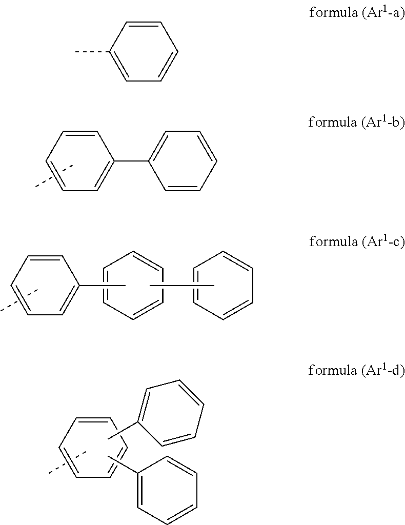
where a radical R1 may be bonded at each of the free positions and the group is bonded to the parent structure of the formula (I) via the dashed bond.

where a group R1 may be bonded at each of the free positions, and
where e may in each case, identically or differently, be 0 or 1, and
where the group is bonded to the parent structure of the formula (I) via the dashed bond.

where a radical R1 may be bonded at each of the free positions and the group is bonded to the parent structure of the formula (I) via the dashed bond.


where the symbols occurring are as defined above and Ar1A, Ar1B, Ar1C and Ar1D is defined like Ar1 and Ar2A and Ar2B are defined like Ar2.


where the symbols occurring are as defined above and Ar1A and Ar1B are defined like Ar1 and Ar2A is defined like Ar2.
| Parent | ||||||||
| structure | Ar1A | Ar1B | Ar1C | Ar1D | Ar2A | Ar2B | ||
| (I-1-1) | (I-1) | (Ar1-a) | — | — | — | — | — |
| (I-1-2) | (I-1) | (Ar1-b) | — | — | — | — | — |
| (I-1-3) | (I-1) | (Ar1-c) | — | — | — | — | — |
| (I-1-4) | (I-1) | (Ar1-d) | — | — | — | — | — |
| (I-2-1) | (I-2) | (Ar1-a) | (Ar1-a) | — | — | — | — |
| (I-2-2) | (I-2) | (Ar1-a) | (Ar1-b) | — | — | — | — |
| (I-2-3) | (I-2) | (Ar1-a) | (Ar1-c) | — | — | — | — |
| (I-2-4) | (I-2) | (Ar1-a) | (Ar1-d) | — | — | — | — |
| (I-2-5) | (I-2) | (Ar1-b) | (Ar1-b) | — | — | — | — |
| (I-2-6) | (I-2) | (Ar1-b) | (Ar1-c) | — | — | — | — |
| (I-2-7) | (I-2) | (Ar1-b) | (Ar1-d) | — | — | — | — |
| (I-2-8) | (I-2) | (Ar1-c) | (Ar1-c) | — | — | — | — |
| (I-2-9) | (I-2) | (Ar1-c) | (Ar1-d) | — | — | — | — |
| (I-2-10) | (I-2) | (Ar1-d) | (Ar1-d) | — | — | — | — |
| (I-3-1) | (I-3) | (Ar1-a) | (Ar1-a) | (Ar1-a) | — | — | — |
| (I-3-2) | (I-3) | (Ar1-a) | (Ar1-b) | (Ar1-a) | — | — | — |
| (I-3-3) | (I-3) | (Ar1-a) | (Ar1-c) | (Ar1-a) | — | — | — |
| (I-3-4) | (I-3) | (Ar1-a) | (Ar1-d) | (Ar1-a) | — | — | — |
| (I-3-5) | (I-3) | (Ar1-b) | (Ar1-b) | (Ar1-a) | — | — | — |
| (I-3-6) | (I-3) | (Ar1-b) | (Ar1-c) | (Ar1-a) | — | — | — |
| (I-3-7) | (I-3) | (Ar1-b) | (Ar1-d) | (Ar1-a) | — | — | — |
| (I-3-8) | (I-3) | (Ar1-c) | (Ar1-c) | (Ar1-a) | — | — | — |
| (I-3-9) | (I-3) | (Ar1-c) | (Ar1-d) | (Ar1-a) | — | — | — |
| (I-3-10) | (I-3) | (Ar1-d) | (Ar1-d) | (Ar1-a) | — | — | — |
| (I-3-11) | (I-3) | (Ar1-a) | (Ar1-a) | (Ar1-b) | — | — | — |
| (I-3-12) | (I-3) | (Ar1-a) | (Ar1-b) | (Ar1-b) | — | — | — |
| (I-3-13) | (I-3) | (Ar1-a) | (Ar1-c) | (Ar1-b) | — | — | — |
| (I-3-14) | (I-3) | (Ar1-a) | (Ar1-d) | (Ar1-b) | — | — | — |
| (I-3-15) | (I-3) | (Ar1-b) | (Ar1-b) | (Ar1-b) | — | — | — |
| (I-3-16) | (I-3) | (Ar1-b) | (Ar1-c) | (Ar1-b) | — | — | — |
| (I-3-17) | (I-3) | (Ar1-b) | (Ar1-d) | (Ar1-b) | — | — | — |
| (I-3-18) | (I-3) | (Ar1-c) | (Ar1-c) | (Ar1-b) | — | — | — |
| (I-3-19) | (I-3) | (Ar1-c) | (Ar1-d) | (Ar1-b) | — | — | — |
| (I-3-20) | (I-3) | (Ar1-d) | (Ar1-d) | (Ar1-b) | — | — | — |
| (I-3-21) | (I-3) | (Ar1-a) | (Ar1-a) | (Ar1-c) | — | — | — |
| (I-3-22) | (I-3) | (Ar1-a) | (Ar1-b) | (Ar1-c) | — | — | — |
| (I-3-23) | (I-3) | (Ar1-a) | (Ar1-c) | (Ar1-c) | — | — | — |
| (I-3-24) | (I-3) | (Ar1-a) | (Ar1-d) | (Ar1-c) | — | — | — |
| (I-3-25) | (I-3) | (Ar1-b) | (Ar1-b) | (Ar1-c) | — | — | — |
| (I-3-26) | (I-3) | (Ar1-b) | (Ar1-c) | (Ar1-c) | — | — | — |
| (I-3-27) | (I-3) | (Ar1-b) | (Ar1-d) | (Ar1-c) | — | — | — |
| (I-3-28) | (I-3) | (Ar1-c) | (Ar1-c) | (Ar1-c) | — | — | — |
| (I-3-29) | (I-3) | (Ar1-c) | (Ar1-d) | (Ar1-c) | — | — | — |
| (I-3-30) | (I-3) | (Ar1-d) | (Ar1-d) | (Ar1-c) | — | — | — |
| (I-3-31) | (I-3) | (Ar1-a) | (Ar1-a) | (Ar1-d) | — | — | — |
| (I-3-32) | (I-3) | (Ar1-a) | (Ar1-b) | (Ar1-d) | — | — | — |
| (I-3-33) | (I-3) | (Ar1-a) | (Ar1-c) | (Ar1-d) | — | — | — |
| (I-3-34) | (I-3) | (Ar1-a) | (Ar1-d) | (Ar1-d) | — | — | — |
| (I-3-35) | (I-3) | (Ar1-b) | (Ar1-b) | (Ar1-d) | — | — | — |
| (I-3-36) | (I-3) | (Ar1-b) | (Ar1-c) | (Ar1-d) | — | — | — |
| (I-3-37) | (I-3) | (Ar1-b) | (Ar1-d) | (Ar1-d) | — | — | — |
| (I-3-38) | (I-3) | (Ar1-c) | (Ar1-c) | (Ar1-d) | — | — | — |
| (I-3-39) | (I-3) | (Ar1-c) | (Ar1-d) | (Ar1-d) | — | — | — |
| (I-3-40) | (I-3) | (Ar1-d) | (Ar1-d) | (Ar1-d) | — | — | — |
| (I-5-1) | (I-5) | (Ar1-a) | — | — | — | (Ar2-a) | — |
| (I-5-2) | (I-5) | (Ar1-a) | — | — | — | (Ar2-b) | — |
| (I-5-3) | (I-5) | (Ar1-b) | — | — | — | (Ar2-a) | — |
| (I-5-4) | (I-5) | (Ar1-b) | — | — | — | (Ar2-b) | — |
| (I-5-5) | (I-5) | (Ar1-c) | — | — | — | (Ar2-a) | — |
| (I-5-6) | (I-5) | (Ar1-c) | — | — | — | (Ar2-b) | — |
| (I-5-7) | (I-5) | (Ar1-d) | — | — | — | (Ar2-a) | — |
| (I-5-8) | (I-5) | (Ar1-d) | — | — | — | (Ar2-b) | — |
| (I-6-1) | (I-6) | (Ar1-a) | (Ar1-a) | — | — | (Ar2-a) | — |
| (I-6-2) | (I-6) | (Ar1-a) | (Ar1-b) | — | — | (Ar2-a) | — |
| (I-6-3) | (I-6) | (Ar1-a) | (Ar1-c) | — | — | (Ar2-a) | — |
| (I-6-4) | (I-6) | (Ar1-a) | (Ar1-d) | — | — | (Ar2-a) | — |
| (I-6-5) | (I-6) | (Ar1-b) | (Ar1-b) | — | — | (Ar2-a) | — |
| (I-6-6) | (I-6) | (Ar1-b) | (Ar1-c) | — | — | (Ar2-a) | — |
| (I-6-7) | (I-6) | (Ar1-b) | (Ar1-d) | — | — | (Ar2-a) | — |
| (I-6-8) | (I-6) | (Ar1-c) | (Ar1-c) | — | — | (Ar2-a) | — |
| (I-6-9) | (I-6) | (Ar1-c) | (Ar1-d) | — | — | (Ar2-a) | — |
| (I-6-10) | (I-6) | (Ar1-d) | (Ar1-d) | — | — | (Ar2-a) | — |
| (I-6-11) | (I-6) | (Ar1-a) | (Ar1-a) | — | — | (Ar2-b) | — |
| (I-6-12) | (I-6) | (Ar1-a) | (Ar1-b) | — | — | (Ar2-b) | — |
| (I-6-13) | (I-6) | (Ar1-a) | (Ar1-c) | — | — | (Ar2-b) | — |
| (I-6-14) | (I-6) | (Ar1-a) | (Ar1-d) | — | — | (Ar2-b) | — |
| (I-6-15) | (I-6) | (Ar1-b) | (Ar1-b) | — | — | (Ar2-b) | — |
| (I-6-16) | (I-6) | (Ar1-b) | (Ar1-c) | — | — | (Ar2-b) | — |
| (I-6-17) | (I-6) | (Ar1-b) | (Ar1-d) | — | — | (Ar2-b) | — |
| (I-6-18) | (I-6) | (Ar1-c) | (Ar1-c) | — | — | (Ar2-b) | — |
| (I-6-19) | (I-6) | (Ar1-c) | (Ar1-d) | — | — | (Ar2-b) | — |
| (I-6-20) | (I-6) | (Ar1-d) | (Ar1-d) | — | — | (Ar2-b) | — |
| (I-7-1) | (I-7) | (Ar1-a) | (Ar1-a) | (Ar1-a) | — | (Ar2-a) | — |
| (I-7-2) | (I-7) | (Ar1-a) | (Ar1-b) | (Ar1-a) | — | (Ar2-a) | — |
| (I-7-3) | (I-7) | (Ar1-a) | (Ar1-c) | (Ar1-a) | — | (Ar2-a) | — |
| (I-7-4) | (I-7) | (Ar1-a) | (Ar1-d) | (Ar1-a) | — | (Ar2-a) | — |
| (I-7-5) | (I-7) | (Ar1-b) | (Ar1-b) | (Ar1-a) | — | (Ar2-a) | — |
| (I-7-6) | (I-7) | (Ar1-b) | (Ar1-c) | (Ar1-a) | — | (Ar2-a) | — |
| (I-7-7) | (I-7) | (Ar1-b) | (Ar1-d) | (Ar1-a) | — | (Ar2-a) | — |
| (I-7-8) | (I-7) | (Ar1-c) | (Ar1-c) | (Ar1-a) | — | (Ar2-a) | — |
| (I-7-9) | (I-7) | (Ar1-c) | (Ar1-d) | (Ar1-a) | — | (Ar2-a) | — |
| (I-7-10) | (I-7) | (Ar1-d) | (Ar1-d) | (Ar1-a) | — | (Ar2-a) | — |
| (I-7-11) | (I-7) | (Ar1-a) | (Ar1-a) | (Ar1-b) | — | (Ar2-a) | — |
| (I-7-12) | (I-7) | (Ar1-a) | (Ar1-b) | (Ar1-b) | — | (Ar2-a) | — |
| (I-7-13) | (I-7) | (Ar1-a) | (Ar1-c) | (Ar1-b) | — | (Ar2-a) | — |
| (I-7-14) | (I-7) | (Ar1-a) | (Ar1-d) | (Ar1-b) | — | (Ar2-a) | — |
| (I-7-15) | (I-7) | (Ar1-b) | (Ar1-b) | (Ar1-b) | — | (Ar2-a) | — |
| (I-7-16) | (I-7) | (Ar1-b) | (Ar1-c) | (Ar1-b) | — | (Ar2-a) | — |
| (I-7-17) | (I-7) | (Ar1-b) | (Ar1-d) | (Ar1-b) | — | (Ar2-a) | — |
| (I-7-18) | (I-7) | (Ar1-c) | (Ar1-c) | (Ar1-b) | — | (Ar2-a) | — |
| (I-7-19) | (I-7) | (Ar1-c) | (Ar1-d) | (Ar1-b) | — | (Ar2-a) | — |
| (I-7-20) | (I-7) | (Ar1-d) | (Ar1-d) | (Ar1-b) | — | (Ar2-a) | — |
| (I-7-21) | (I-7) | (Ar1-a) | (Ar1-a) | (Ar1-c) | — | (Ar2-a) | — |
| (I-7-22) | (I-7) | (Ar1-a) | (Ar1-b) | (Ar1-c) | — | (Ar2-a) | — |
| (I-7-23) | (I-7) | (Ar1-a) | (Ar1-c) | (Ar1-c) | — | (Ar2-a) | — |
| (I-7-24) | (I-7) | (Ar1-a) | (Ar1-d) | (Ar1-c) | — | (Ar2-a) | — |
| (I-7-25) | (I-7) | (Ar1-b) | (Ar1-b) | (Ar1-c) | — | (Ar2-a) | — |
| (I-7-26) | (I-7) | (Ar1-b) | (Ar1-c) | (Ar1-c) | — | (Ar2-a) | — |
| (I-7-27) | (I-7) | (Ar1-b) | (Ar1-d) | (Ar1-c) | — | (Ar2-a) | — |
| (I-7-28) | (I-7) | (Ar1-c) | (Ar1-c) | (Ar1-c) | — | (Ar2-a) | — |
| (I-7-29) | (I-7) | (Ar1-c) | (Ar1-d) | (Ar1-c) | — | (Ar2-a) | — |
| (I-7-30) | (I-7) | (Ar1-d) | (Ar1-d) | (Ar1-c) | — | (Ar2-a) | — |
| (I-7-31) | (I-7) | (Ar1-a) | (Ar1-a) | (Ar1-d) | — | (Ar2-a) | — |
| (I-7-32) | (I-7) | (Ar1-a) | (Ar1-b) | (Ar1-d) | — | (Ar2-a) | — |
| (I-7-33) | (I-7) | (Ar1-a) | (Ar1-c) | (Ar1-d) | — | (Ar2-a) | — |
| (I-7-34) | (I-7) | (Ar1-a) | (Ar1-d) | (Ar1-d) | — | (Ar2-a) | — |
| (I-7-35) | (I-7) | (Ar1-b) | (Ar1-b) | (Ar1-d) | — | (Ar2-a) | — |
| (I-7-36) | (I-7) | (Ar1-b) | (Ar1-c) | (Ar1-d) | — | (Ar2-a) | — |
| (I-7-37) | (I-7) | (Ar1-b) | (Ar1-d) | (Ar1-d) | — | (Ar2-a) | — |
| (I-7-38) | (I-7) | (Ar1-c) | (Ar1-c) | (Ar1-d) | — | (Ar2-a) | — |
| (I-7-39) | (I-7) | (Ar1-c) | (Ar1-d) | (Ar1-d) | — | (Ar2-a) | — |
| (I-7-40) | (I-7) | (Ar1-d) | (Ar1-d) | (Ar1-d) | — | (Ar2-a) | — |
| (I-7-41) | (I-7) | (Ar1-a) | (Ar1-a) | (Ar1-a) | — | (Ar2-b) | — |
| (I-7-42) | (I-7) | (Ar1-a) | (Ar1-b) | (Ar1-a) | — | (Ar2-b) | — |
| (I-7-43) | (I-7) | (Ar1-a) | (Ar1-c) | (Ar1-a) | — | (Ar2-b) | — |
| (I-7-44) | (I-7) | (Ar1-a) | (Ar1-d) | (Ar1-a) | — | (Ar2-b) | — |
| (I-7-45) | (I-7) | (Ar1-b) | (Ar1-b) | (Ar1-a) | — | (Ar2-b) | — |
| (I-7-46) | (I-7) | (Ar1-b) | (Ar1-c) | (Ar1-a) | — | (Ar2-b) | — |
| (I-7-47) | (I-7) | (Ar1-b) | (Ar1-d) | (Ar1-a) | — | (Ar2-b) | — |
| (I-7-48) | (I-7) | (Ar1-c) | (Ar1-c) | (Ar1-a) | — | (Ar2-b) | — |
| (I-7-49) | (I-7) | (Ar1-c) | (Ar1-d) | (Ar1-a) | — | (Ar2-b) | — |
| (I-7-50) | (I-7) | (Ar1-d) | (Ar1-d) | (Ar1-a) | — | (Ar2-b) | — |
| (I-7-51) | (I-7) | (Ar1-a) | (Ar1-a) | (Ar1-b) | — | (Ar2-b) | — |
| (I-7-52) | (I-7) | (Ar1-a) | (Ar1-b) | (Ar1-b) | — | (Ar2-b) | — |
| (I-7-53) | (I-7) | (Ar1-a) | (Ar1-c) | (Ar1-b) | — | (Ar2-b) | — |
| (I-7-54) | (I-7) | (Ar1-a) | (Ar1-d) | (Ar1-b) | — | (Ar2-b) | — |
| (I-7-55) | (I-7) | (Ar1-b) | (Ar1-b) | (Ar1-b) | — | (Ar2-b) | — |
| (I-7-56) | (I-7) | (Ar1-b) | (Ar1-c) | (Ar1-b) | — | (Ar2-b) | — |
| (I-7-57) | (I-7) | (Ar1-b) | (Ar1-d) | (Ar1-b) | — | (Ar2-b) | — |
| (I-7-58) | (I-7) | (Ar1-c) | (Ar1-c) | (Ar1-b) | — | (Ar2-b) | — |
| (I-7-59) | (I-7) | (Ar1-c) | (Ar1-d) | (Ar1-b) | — | (Ar2-b) | — |
| (I-7-60) | (I-7) | (Ar1-d) | (Ar1-d) | (Ar1-b) | — | (Ar2-b) | — |
| (I-7-61) | (I-7) | (Ar1-a) | (Ar1-a) | (Ar1-c) | — | (Ar2-b) | — |
| (I-7-62) | (I-7) | (Ar1-a) | (Ar1-b) | (Ar1-c) | — | (Ar2-b) | — |
| (I-7-63) | (I-7) | (Ar1-a) | (Ar1-c) | (Ar1-c) | — | (Ar2-b) | — |
| (I-7-64) | (I-7) | (Ar1-a) | (Ar1-d) | (Ar1-c) | — | (Ar2-b) | — |
| (I-7-65) | (I-7) | (Ar1-b) | (Ar1-b) | (Ar1-c) | — | (Ar2-b) | — |
| (I-7-66) | (I-7) | (Ar1-b) | (Ar1-c) | (Ar1-c) | — | (Ar2-b) | — |
| (I-7-67) | (I-7) | (Ar1-b) | (Ar1-d) | (Ar1-c) | — | (Ar2-b) | — |
| (I-7-68) | (I-7) | (Ar1-c) | (Ar1-c) | (Ar1-c) | — | (Ar2-b) | — |
| (I-7-69) | (I-7) | (Ar1-c) | (Ar1-d) | (Ar1-c) | — | (Ar2-b) | — |
| (I-7-70) | (I-7) | (Ar1-d) | (Ar1-d) | (Ar1-c) | — | (Ar2-b) | — |
| (I-7-71) | (I-7) | (Ar1-a) | (Ar1-a) | (Ar1-d) | — | (Ar2-b) | — |
| (I-7-72) | (I-7) | (Ar1-a) | (Ar1-b) | (Ar1-d) | — | (Ar2-b) | — |
| (I-7-73) | (I-7) | (Ar1-a) | (Ar1-c) | (Ar1-d) | — | (Ar2-b) | — |
| (I-7-74) | (I-7) | (Ar1-a) | (Ar1-d) | (Ar1-d) | — | (Ar2-b) | — |
| (I-7-75) | (I-7) | (Ar1-b) | (Ar1-b) | (Ar1-d) | — | (Ar2-b) | — |
| (I-7-76) | (I-7) | (Ar1-b) | (Ar1-c) | (Ar1-d) | — | (Ar2-b) | — |
| (I-7-77) | (I-7) | (Ar1-b) | (Ar1-d) | (Ar1-d) | — | (Ar2-b) | — |
| (I-7-78) | (I-7) | (Ar1-c) | (Ar1-c) | (Ar1-d) | — | (Ar2-b) | — |
| (I-7-79) | (I-7) | (Ar1-c) | (Ar1-d) | (Ar1-d) | — | (Ar2-b) | — |
| (I-7-80) | (I-7) | (Ar1-d) | (Ar1-d) | (Ar1-d) | — | (Ar2-b) | — |
 |
1 |
 |
2 |
 |
3 |
 |
4 |
 |
5 |
 |
6 |
 |
7 |
 |
8 |
 |
9 |
 |
10 |
 |
11 |
 |
12 |
 |
13 |
 |
14 |
 |
14 |
 |
16 |
 |
17 |
 |
18 |
 |
19 |
 |
20 |
 |
21 |
 |
22 |
 |
23 |
 |
24 |
 |
25 |
 |
26 |
 |
27 |
 |
28 |
 |
29 |
 |
30 |
 |
31 |
 |
32 |


 |
 |
 |
 |
 |
 |
 |
 |
 |
 |
 |
 |
 |
 |
 |
 |
 |
 |
 |
 |
 |
 |
 |
 |
 |
 |
 |
 |
 |
 |
 |
 |
 |
 |
 |
 |
 |
 |
 |
 |
 |
 |
 |
 |
 |
 |
 |
 |
 |
 |
 |
 |
 |
 |
 |
 |
 |
 |
 |
 |
 |
 |
 |
 |
 |
 |
 |
 |
 |
 |
 |
 |
 |
 |
 |
 |
 |
 |
 |
 |
 |
 |
 |
 |
 |
 |
 |
 |
 |
 |
 |
 |
 |
 |
 |
 |
 |
 |
 |
 |
 |
 |
 |
 |
 |
 |
 |
 |
 |
 |
 |
 |
 |
 |
 |
 |
 |
 |
 |
 |
 |
 |
 |
 |
 |
 |
 |
 |
 |
 |
 |
 |
 |
 |
 |
 |
 |
 |
 |
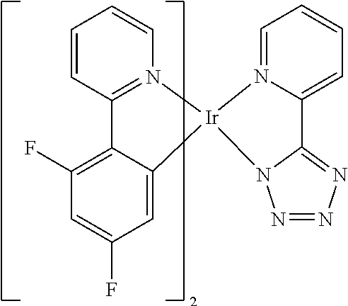 |
 |
 |
 |
 |
 |
 |
 |
 |
 |
 |

| Ex. | sec-Amine | Bromide | tert-Amine | Yield |
| 2 |
 |
 |
 |
34% |
| 3 |
 |
 |
 |
29% |
| 4 |
 |
 |
 |
23% |
| 5 |
 |
 |
 |
26% |
| 6 |
 |
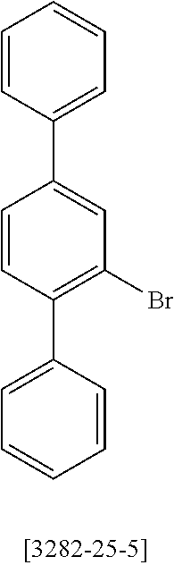 |
 |
20% |
| 7 |
 |
 |
 |
36% |
| 8 |
 |
 |
 |
30% |
| 9 |
 |
 |
 |
27% |

| TABLE 1 |
| Structure of the OLEDs |
| IL | HTL | IL | HTL2 | EBL | EML | ETL | |
| Ex. | Thickness/nm | Thickness/nm | Thickness/nm | Thickness/nm | Thickness/nm | Thickness/nm | Thickness/nm |
| V1 | HIL1 | HIL2 | HIL1 | NPB | H1(95%):SEB1(5%) | ETM1(50%):LiQ(50%) | |
| 5 nm | 140 nm | 5 nm | 20 nm | 20 nm | 30 nm | ||
| V2 | HIL1 | HIL2 | HIL1 | NPB | HTMV1 | H1(95%):SEB1(5%) | ETM1(50%):LiQ(50%) |
| 5 nm | 130 nm | 5 nm | 10 nm | 20 nm | 20 nm | 30 nm | |
| V3 | HIL1 | HIL2 | HIL1 | NPB | HTMV2 | H1(95%):SEB1(5%) | ETM1(50%):LiQ(50%) |
| 5 nm | 130 nm | 5 nm | 10 nm | 20 nm | 20 nm | 30 nm | |
| E1 | HIL1 | HIL2 | HIL1 | NPB | HTM1 | H1(95%):SEB1(5%) | ETM1(50%):LiQ(50%) |
| 5 nm | 130 nm | 5 nm | 10 nm | 20 nm | 20 nm | 30 nm | |
| E2 | HIL1 | HIL2 | HIL1 | NPB | HTM2 | H1(95%):SEB1(5%) | ETM1(50%):LiQ(50%) |
| 5 nm | 130 nm | 5 nm | 10 nm | 20 nm | 20 nm | 30 nm | |
| E3 | HIL1 | HIL2 | HIL1 | NPB | HTM3 | H1(95%):SEB1(5%) | ETM1(50%):LiQ(50%) |
| 5 nm | 130 nm | 5 nm | 10 nm | 20 nm | 20 nm | 30 nm | |
| E4 | HIL1 | HIL2 | HIL1 | NPB | HTM4 | H1(95%):SEB1(5%) | ETM1(50%):LiQ(50%) |
| 5 nm | 130 nm | 5 nm | 10 nm | 20 nm | 20 nm | 30 nm | |
| E5 | HIL1 | HIL2 | HIL1 | NPB | HTM5 | H1(95%):SEB1(5%) | ETM1(50%):LiQ(50%) |
| 5 nm | 130 nm | 5 nm | 10 nm | 20 nm | 20 nm | 30 nm | |
| E6 | HIL1 | HIL2 | HIL1 | NPB | HTM6 | H1(95%):SEB1(5%) | ETM1(50%):LiQ(50%) |
| 5 nm | 130 nm | 5 nm | 10 nm | 20 nm | 20 nm | 30 nm | |
| TABLE 2 |
| Data of the OLEDs |
| U @ | EQE | LT80 | ||
| 1000 cd/m2 | @ 1000 cd/m2 | @ 6000 cd/m2 | CIE |
| Ex. | V | % | [h] | x | y |
| V1 | 4.7 | 4.8 | 70 | 0.14 | 0.17 |
| V2 | 4.2 | 7.7 | 100 | 0.14 | 0.16 |
| V3 | 4.6 | 7.6 | 115 | 0.14 | 0.16 |
| E1 | 4.5 | 7.5 | 120 | 0.14 | 0.15 |
| E2 | 4.6 | 7.6 | 125 | 0.14 | 0.16 |
| E3 | 4.5 | 7.5 | 120 | 0.14 | 0.16 |
| E4 | 4.6 | 7.6 | 130 | 0.14 | 0.15 |
| E5 | 4.5 | 7.5 | 120 | 0.14 | 0.16 |
| E6 | 4.4 | 7.4 | 120 | 0.14 | 0.16 |
| TABLE 3 |
| Structure of the OLEDs |
| HTL | IL | HTL2 | EBL | EML | ETL | |
| Ex. | Thickness/nm | Thickness/nm | Thickness/nm | Thickness/nm | Thickness/nm | Thickness/nm |
| V4 | HIL2 | HIL1 | NPB | H2(88%):Irpy(12%) | ETM1(50%):LiQ(50%) | |
| 70 nm | 5 nm | 90 nm | 30 nm | 40 nm | ||
| V5 | HIL2 | HIL1 | NPB | HTMV1 | H2(88%):Irpy(12%) | ETM1(50%):LiQ(50%) |
| 70 nm | 5 nm | 10 nm | 80 nm | 30 nm | 40 nm | |
| V6 | HIL2 | HIL1 | NPB | HTMV2 | H2(88%):Irpy(12%) | ETM1(50%):LiQ(50%) |
| 70 nm | 5 nm | 10 nm | 80 nm | 30 nm | 40 nm | |
| E7 | HIL2 | HIL1 | NPB | HTM1 | H2(88%):Irpy(12%) | ETM1(50%):LiQ(50%) |
| 70 nm | 5 nm | 10 nm | 80 nm | 30 nm | 40 nm | |
| E8 | HIL2 | HIL1 | NPB | HTM2 | H2(88%):Irpy(12%) | ETM1(50%):LiQ(50%) |
| 70 nm | 5 nm | 10 nm | 80 nm | 30 nm | 40 nm | |
| E9 | HIL2 | HIL1 | NPB | HTM3 | H2(88%):Irpy(12%) | ETM1(50%):LiQ(50%) |
| 70 nm | 5 nm | 10 nm | 80 nm | 30 nm | 40 nm | |
| E10 | HIL2 | HIL1 | NPB | HTM2 | H2(88%):Irpy(12%) | ETM1(50%):LiQ(50%) |
| 70 nm | 5 nm | 10 nm | 80 nm | 30 nm | 40 nm | |
| E11 | HIL2 | HIL1 | NPB | HTM3 | H2(88%):Irpy(12%) | ETM1(50%):LiQ(50%) |
| 70 nm | 5 nm | 10 nm | 80 nm | 30 nm | 40 nm | |
| E12 | HIL2 | HIL1 | NPB | HTM2 | H2(88%):Irpy(12%) | ETM1(50%):LiQ(50%) |
| 70 nm | 5 nm | 10 nm | 80 nm | 30 nm | 40 nm | |
| TABLE 4 |
| Data of the OLEDs |
| U @ | EQE | LT80 | ||
| 1000 cd/m2 | @ 1000 cd/m2 | @ 8000 cd/m2 | CIE |
| Ex. | V | % | [h] | x | y |
| V4 | 3.6 | 14.4 | 85 | 0.32 | 0.63 |
| V5 | 3.6 | 17.8 | 120 | 0.35 | 0.62 |
| V6 | 3.6 | 17.8 | 115 | 0.34 | 0.62 |
| E7 | 3.5 | 17.7 | 145 | 0.34 | 0.63 |
| E8 | 3.5 | 17.3 | 150 | 0.36 | 0.62 |
| E9 | 3.6 | 17.5 | 140 | 0.35 | 0.62 |
| E10 | 3.6 | 17.8 | 125 | 0.34 | 0.63 |
| E11 | 3.6 | 17.7 | 145 | 0.35 | 0.63 |
| E12 | 3.5 | 17.3 | 145 | 0.35 | 0.62 |
| TABLE 5 |
| Structures of the materials used |
 |
HIL1 |
 |
HIL2 |
 |
NPB |
 |
ETM1 |
 |
AlQ3 |
 |
H1 |
 |
SEB1 |
 |
LiQ |
 |
H2 |
 |
Irpy |
 |
HTMV1 |
 |
HTMV2 |
 |
HTM1 |
 |
HTM2 |
 |
HTM3 |
 |
HTM4 |
 |
HTM5 |
 |
HTM6 |
Claims (12)


Priority Applications (1)
| Application Number | Priority Date | Filing Date | Title |
|---|---|---|---|
| US15/987,480 US10665787B2 (en) | 2011-12-12 | 2018-05-23 | Compounds for electronic devices |
Applications Claiming Priority (6)
| Application Number | Priority Date | Filing Date | Title |
|---|---|---|---|
| EP11009779 | 2011-12-12 | ||
| EP11009779.7 | 2011-12-12 | ||
| EP11009779 | 2011-12-12 | ||
| PCT/EP2012/004744 WO2013087142A1 (en) | 2011-12-12 | 2012-11-15 | Compounds for electronic devices |
| US201414364120A | 2014-06-10 | 2014-06-10 | |
| US15/987,480 US10665787B2 (en) | 2011-12-12 | 2018-05-23 | Compounds for electronic devices |
Related Parent Applications (2)
| Application Number | Title | Priority Date | Filing Date |
|---|---|---|---|
| PCT/EP2012/004744 Continuation WO2013087142A1 (en) | 2011-12-12 | 2012-11-15 | Compounds for electronic devices |
| US14/364,120 Continuation US10008672B2 (en) | 2011-12-12 | 2012-11-15 | Compounds for electronic devices |
Publications (2)
| Publication Number | Publication Date |
|---|---|
| US20180269398A1 US20180269398A1 (en) | 2018-09-20 |
| US10665787B2 true US10665787B2 (en) | 2020-05-26 |
Family
ID=47216194
Family Applications (3)
| Application Number | Title | Priority Date | Filing Date |
|---|---|---|---|
| US14/364,120 Active 2035-04-11 US10008672B2 (en) | 2011-12-12 | 2012-11-15 | Compounds for electronic devices |
| US15/987,533 Active US10424739B2 (en) | 2011-12-12 | 2018-05-23 | Compounds for electronic devices |
| US15/987,480 Active US10665787B2 (en) | 2011-12-12 | 2018-05-23 | Compounds for electronic devices |
Family Applications Before (2)
| Application Number | Title | Priority Date | Filing Date |
|---|---|---|---|
| US14/364,120 Active 2035-04-11 US10008672B2 (en) | 2011-12-12 | 2012-11-15 | Compounds for electronic devices |
| US15/987,533 Active US10424739B2 (en) | 2011-12-12 | 2018-05-23 | Compounds for electronic devices |
Country Status (6)
| Country | Link |
|---|---|
| US (3) | US10008672B2 (en) |
| EP (1) | EP2791105B1 (en) |
| JP (2) | JP6570834B2 (en) |
| KR (3) | KR20180126629A (en) |
| CN (2) | CN103998415B (en) |
| WO (1) | WO2013087142A1 (en) |
Families Citing this family (87)
| Publication number | Priority date | Publication date | Assignee | Title |
|---|---|---|---|---|
| WO2013087142A1 (en) * | 2011-12-12 | 2013-06-20 | Merck Patent Gmbh | Compounds for electronic devices |
| WO2014034795A1 (en) | 2012-08-31 | 2014-03-06 | 出光興産株式会社 | Aromatic amine derivative, and organic electroluminescent element using same |
| CN105431956B (en) * | 2013-07-29 | 2020-02-28 | 默克专利有限公司 | Electro-optical device and use thereof |
| US20160163987A1 (en) * | 2013-07-29 | 2016-06-09 | Merck Patent Gmbh | Electro-optical device and the use thereof |
| EP4345089A2 (en) | 2013-10-11 | 2024-04-03 | Idemitsu Kosan Co.,Ltd. | Aromatic amine compound, organic electroluminescent element and electronic device |
| KR20230080505A (en) * | 2014-02-28 | 2023-06-07 | 이데미쓰 고산 가부시키가이샤 | Compound, material for organic electroluminescent element, organic electroluminescent element, and electronic apparatus |
| CN106688119B (en) * | 2014-07-09 | 2019-07-23 | 保土谷化学工业株式会社 | Organic electroluminescence device |
| EP3127894B1 (en) | 2014-07-11 | 2021-04-28 | Idemitsu Kosan Co., Ltd. | Compound, material for organic electroluminescent element, organic electroluminescent element, and electronic device |
| KR102572370B1 (en) | 2014-07-11 | 2023-08-29 | 이데미쓰 고산 가부시키가이샤 | Compound, material for organic electroluminescent element, organic electroluminescent element, and electronic device |
| JP6552802B2 (en) | 2014-10-21 | 2019-07-31 | 三星ディスプレイ株式會社Samsung Display Co.,Ltd. | Material for organic electroluminescence device and organic electroluminescence device using the same |
| JP2016108290A (en) | 2014-12-09 | 2016-06-20 | 三星ディスプレイ株式會社Samsung Display Co.,Ltd. | Amine derivative and organic electroluminescent element |
| US10497876B2 (en) * | 2014-12-24 | 2019-12-03 | Hodogaya Chemical Co., Ltd. | Organic electroluminescent device |
| KR102433462B1 (en) | 2014-12-30 | 2022-08-17 | 메르크 파텐트 게엠베하 | Compositions comprising at least one polymer and at least one salt, and electroluminescent devices containing said compositions |
| US10505119B2 (en) * | 2015-01-08 | 2019-12-10 | Hodogaya Chemical Co., Ltd. | Organic electroluminescence device |
| JP6715781B2 (en) * | 2015-02-03 | 2020-07-01 | 保土谷化学工業株式会社 | Organic electroluminescent device |
| US9929361B2 (en) | 2015-02-16 | 2018-03-27 | Universal Display Corporation | Organic electroluminescent materials and devices |
| US11056657B2 (en) | 2015-02-27 | 2021-07-06 | University Display Corporation | Organic electroluminescent materials and devices |
| US9859510B2 (en) | 2015-05-15 | 2018-01-02 | Universal Display Corporation | Organic electroluminescent materials and devices |
| US10418568B2 (en) | 2015-06-01 | 2019-09-17 | Universal Display Corporation | Organic electroluminescent materials and devices |
| US11127905B2 (en) | 2015-07-29 | 2021-09-21 | Universal Display Corporation | Organic electroluminescent materials and devices |
| US10672996B2 (en) | 2015-09-03 | 2020-06-02 | Universal Display Corporation | Organic electroluminescent materials and devices |
| US20180362843A1 (en) * | 2015-12-08 | 2018-12-20 | Hodogaya Chemical Co., Ltd. | Organic electroluminescent device |
| US20170229663A1 (en) | 2016-02-09 | 2017-08-10 | Universal Display Corporation | Organic electroluminescent materials and devices |
| US10236456B2 (en) | 2016-04-11 | 2019-03-19 | Universal Display Corporation | Organic electroluminescent materials and devices |
| US10862054B2 (en) | 2016-06-20 | 2020-12-08 | Universal Display Corporation | Organic electroluminescent materials and devices |
| US10672997B2 (en) | 2016-06-20 | 2020-06-02 | Universal Display Corporation | Organic electroluminescent materials and devices |
| US11482683B2 (en) | 2016-06-20 | 2022-10-25 | Universal Display Corporation | Organic electroluminescent materials and devices |
| US10608186B2 (en) | 2016-09-14 | 2020-03-31 | Universal Display Corporation | Organic electroluminescent materials and devices |
| KR20180032735A (en) | 2016-09-22 | 2018-04-02 | 삼성디스플레이 주식회사 | Amine compound and organic electroluminescence device including the same |
| US10680187B2 (en) | 2016-09-23 | 2020-06-09 | Universal Display Corporation | Organic electroluminescent materials and devices |
| US11196010B2 (en) | 2016-10-03 | 2021-12-07 | Universal Display Corporation | Organic electroluminescent materials and devices |
| US11011709B2 (en) | 2016-10-07 | 2021-05-18 | Universal Display Corporation | Organic electroluminescent materials and devices |
| US20180130956A1 (en) | 2016-11-09 | 2018-05-10 | Universal Display Corporation | Organic electroluminescent materials and devices |
| US10680188B2 (en) | 2016-11-11 | 2020-06-09 | Universal Display Corporation | Organic electroluminescent materials and devices |
| KR20180064609A (en) | 2016-12-05 | 2018-06-15 | 삼성디스플레이 주식회사 | Amine compound and organic electroluminescence device including the same |
| US11780865B2 (en) | 2017-01-09 | 2023-10-10 | Universal Display Corporation | Organic electroluminescent materials and devices |
| US10844085B2 (en) | 2017-03-29 | 2020-11-24 | Universal Display Corporation | Organic electroluminescent materials and devices |
| US10944060B2 (en) | 2017-05-11 | 2021-03-09 | Universal Display Corporation | Organic electroluminescent materials and devices |
| US20180370999A1 (en) | 2017-06-23 | 2018-12-27 | Universal Display Corporation | Organic electroluminescent materials and devices |
| US11228010B2 (en) | 2017-07-26 | 2022-01-18 | Universal Display Corporation | Organic electroluminescent materials and devices |
| US11744142B2 (en) | 2017-08-10 | 2023-08-29 | Universal Display Corporation | Organic electroluminescent materials and devices |
| US11605780B2 (en) | 2017-08-28 | 2023-03-14 | Toray Industries, Inc. | Compound, light-emitting element containing the same, display device, and lighting device |
| US20190161504A1 (en) | 2017-11-28 | 2019-05-30 | University Of Southern California | Carbene compounds and organic electroluminescent devices |
| EP3492480B1 (en) | 2017-11-29 | 2021-10-20 | Universal Display Corporation | Organic electroluminescent materials and devices |
| US11937503B2 (en) | 2017-11-30 | 2024-03-19 | Universal Display Corporation | Organic electroluminescent materials and devices |
| JP6957371B2 (en) * | 2018-01-25 | 2021-11-02 | エルジー・ケム・リミテッド | 2- (2'-Diarylaminophenyl) borabenzene derivative and organic electronic devices containing the derivative |
| US11542289B2 (en) | 2018-01-26 | 2023-01-03 | Universal Display Corporation | Organic electroluminescent materials and devices |
| WO2019233429A1 (en) * | 2018-06-07 | 2019-12-12 | 江苏三月光电科技有限公司 | Compound having triarylamine structure as core, and preparation method therefor |
| US20200075870A1 (en) | 2018-08-22 | 2020-03-05 | Universal Display Corporation | Organic electroluminescent materials and devices |
| US11737349B2 (en) | 2018-12-12 | 2023-08-22 | Universal Display Corporation | Organic electroluminescent materials and devices |
| US11780829B2 (en) | 2019-01-30 | 2023-10-10 | The University Of Southern California | Organic electroluminescent materials and devices |
| US20200251664A1 (en) | 2019-02-01 | 2020-08-06 | Universal Display Corporation | Organic electroluminescent materials and devices |
| JP2020158491A (en) | 2019-03-26 | 2020-10-01 | ユニバーサル ディスプレイ コーポレイション | Organic electroluminescent materials and devices |
| CN110156611B (en) * | 2019-05-23 | 2022-11-11 | 武汉尚赛光电科技有限公司 | Phenyl branched luminescent material and organic electroluminescent device thereof |
| US20210032278A1 (en) | 2019-07-30 | 2021-02-04 | Universal Display Corporation | Organic electroluminescent materials and devices |
| US20210047354A1 (en) | 2019-08-16 | 2021-02-18 | Universal Display Corporation | Organic electroluminescent materials and devices |
| US20210135130A1 (en) | 2019-11-04 | 2021-05-06 | Universal Display Corporation | Organic electroluminescent materials and devices |
| US20210217969A1 (en) | 2020-01-06 | 2021-07-15 | Universal Display Corporation | Organic electroluminescent materials and devices |
| US20220336759A1 (en) | 2020-01-28 | 2022-10-20 | Universal Display Corporation | Organic electroluminescent materials and devices |
| KR20220162113A (en) * | 2020-03-31 | 2022-12-07 | 이데미쓰 고산 가부시키가이샤 | Chemical compounds, materials for organic electroluminescent devices, organic electroluminescent devices and electronic devices |
| EP3937268A1 (en) | 2020-07-10 | 2022-01-12 | Universal Display Corporation | Plasmonic oleds and vertical dipole emitters |
| US20220158096A1 (en) | 2020-11-16 | 2022-05-19 | Universal Display Corporation | Organic electroluminescent materials and devices |
| US20220165967A1 (en) | 2020-11-24 | 2022-05-26 | Universal Display Corporation | Organic electroluminescent materials and devices |
| US20220162243A1 (en) | 2020-11-24 | 2022-05-26 | Universal Display Corporation | Organic electroluminescent materials and devices |
| US20220271241A1 (en) | 2021-02-03 | 2022-08-25 | Universal Display Corporation | Organic electroluminescent materials and devices |
| EP4059915A3 (en) | 2021-02-26 | 2022-12-28 | Universal Display Corporation | Organic electroluminescent materials and devices |
| EP4060758A3 (en) | 2021-02-26 | 2023-03-29 | Universal Display Corporation | Organic electroluminescent materials and devices |
| US20220298192A1 (en) | 2021-03-05 | 2022-09-22 | Universal Display Corporation | Organic electroluminescent materials and devices |
| US20220298190A1 (en) | 2021-03-12 | 2022-09-22 | Universal Display Corporation | Organic electroluminescent materials and devices |
| US20220298193A1 (en) | 2021-03-15 | 2022-09-22 | Universal Display Corporation | Organic electroluminescent materials and devices |
| US20220340607A1 (en) | 2021-04-05 | 2022-10-27 | Universal Display Corporation | Organic electroluminescent materials and devices |
| EP4075531A1 (en) | 2021-04-13 | 2022-10-19 | Universal Display Corporation | Plasmonic oleds and vertical dipole emitters |
| US20220352478A1 (en) | 2021-04-14 | 2022-11-03 | Universal Display Corporation | Organic eletroluminescent materials and devices |
| US20220407020A1 (en) | 2021-04-23 | 2022-12-22 | Universal Display Corporation | Organic electroluminescent materials and devices |
| US20230006149A1 (en) | 2021-04-23 | 2023-01-05 | Universal Display Corporation | Organic electroluminescent materials and devices |
| CN117355364A (en) | 2021-05-21 | 2024-01-05 | 默克专利有限公司 | Method for continuously purifying at least one functional material and device for continuously purifying at least one functional material |
| US20230133787A1 (en) | 2021-06-08 | 2023-05-04 | University Of Southern California | Molecular Alignment of Homoleptic Iridium Phosphors |
| WO2022259886A1 (en) | 2021-06-09 | 2022-12-15 | 出光興産株式会社 | Compound, material for organic electroluminescent elements, organic electroluminescent element and electronic device |
| EP4151699A1 (en) | 2021-09-17 | 2023-03-22 | Universal Display Corporation | Organic electroluminescent materials and devices |
| EP4212539A1 (en) | 2021-12-16 | 2023-07-19 | Universal Display Corporation | Organic electroluminescent materials and devices |
| EP4231804A3 (en) | 2022-02-16 | 2023-09-20 | Universal Display Corporation | Organic electroluminescent materials and devices |
| US20230292592A1 (en) | 2022-03-09 | 2023-09-14 | Universal Display Corporation | Organic electroluminescent materials and devices |
| US20230337516A1 (en) | 2022-04-18 | 2023-10-19 | Universal Display Corporation | Organic electroluminescent materials and devices |
| US20230389421A1 (en) | 2022-05-24 | 2023-11-30 | Universal Display Corporation | Organic electroluminescent materials and devices |
| EP4293001A1 (en) | 2022-06-08 | 2023-12-20 | Universal Display Corporation | Organic electroluminescent materials and devices |
| US20240016051A1 (en) | 2022-06-28 | 2024-01-11 | Universal Display Corporation | Organic electroluminescent materials and devices |
| US20240107880A1 (en) | 2022-08-17 | 2024-03-28 | Universal Display Corporation | Organic electroluminescent materials and devices |
Citations (36)
| Publication number | Priority date | Publication date | Assignee | Title |
|---|---|---|---|---|
| EP0376311A2 (en) | 1988-12-29 | 1990-07-04 | Canon Kabushiki Kaisha | Photosensitive member for electrophotography |
| JPH02178667A (en) | 1988-12-29 | 1990-07-11 | Canon Inc | Electrophotographic sensitive body |
| US4992350A (en) | 1988-09-30 | 1991-02-12 | Ricoh Company, Ltd. | Biphenyl compounds and electrophotographic photoconductor comprising the same |
| JPH03118548A (en) | 1989-09-30 | 1991-05-21 | Ricoh Co Ltd | Method for recovering electrophotographic sensitive body from fatigue |
| US5262261A (en) | 1988-12-29 | 1993-11-16 | Canon Kabushiki Kaisha | Photosensitive member for electrophotography |
| JPH0748324A (en) | 1993-06-04 | 1995-02-21 | Dainippon Ink & Chem Inc | Terphenyl derivative and electrophotographic photoreceptor using the same |
| JPH0753955A (en) | 1993-08-12 | 1995-02-28 | Yasuhiko Shirota | Organic el element |
| JPH086267A (en) | 1994-06-23 | 1996-01-12 | Dainippon Ink & Chem Inc | Resin composition for forming photoconductive layer and electrophotographic photoreceptor using same |
| JPH09325508A (en) | 1996-06-03 | 1997-12-16 | Dainippon Ink & Chem Inc | Electrophotographic photoreceptor |
| JPH1095972A (en) | 1996-08-02 | 1998-04-14 | Mitsui Petrochem Ind Ltd | Organic electroluminescent element |
| JP2000219659A (en) | 1999-01-29 | 2000-08-08 | Kyocera Mita Corp | Stilbene derivative, its production and electrophotographic photoreceptor using the same |
| WO2002051958A1 (en) | 2000-12-23 | 2002-07-04 | Johnson Matthey Public Limited Company | Electroactive polyarylamine-type compositions |
| US20020193551A1 (en) | 2001-05-23 | 2002-12-19 | Qibing Pei | Conjugated electroluminescent polymers and associated methods of preparation and use |
| JP2003201472A (en) | 2001-10-26 | 2003-07-18 | Toyo Ink Mfg Co Ltd | Material for organic electroluminescent element and organic electroluminescent element using the same |
| JP2005116247A (en) | 2003-10-06 | 2005-04-28 | Mitsui Chemicals Inc | Organic electroluminescent element and amine compound |
| EP1683804A2 (en) | 2003-11-04 | 2006-07-26 | Takasago International Corporation | Platinum complex and luminescent element |
| WO2006123667A1 (en) | 2005-05-17 | 2006-11-23 | Mitsubishi Chemical Corporation | Monoamine compound, charge-transporting material, and organic electroluminescent device |
| JP2007091719A (en) | 2005-08-30 | 2007-04-12 | Mitsubishi Chemicals Corp | Organic compound, electric charge transport material, material for organic electroluminescent element, electric charge transport material composition, and organic electroluminescent element |
| US20070215889A1 (en) | 2006-03-20 | 2007-09-20 | Semiconductor Energy Laboratory Co., Ltd. | Aromatic amine compound, and light-emitting element, light-emitting device, and electronic appliance using the aromatic amine compound |
| JP2007284431A (en) | 2006-03-20 | 2007-11-01 | Semiconductor Energy Lab Co Ltd | Aromatic amine compound and light-emitting element, light-emitting device and electronic device produced by using aromatic amine compound |
| JP2007318063A (en) | 2005-12-20 | 2007-12-06 | Canon Inc | Organic light-emitting device |
| JP2008239613A (en) | 2007-02-28 | 2008-10-09 | Semiconductor Energy Lab Co Ltd | Quinoxaline derivative, and light-emitting element using quinoxaline derivative, light-emitting device and electronic equipment |
| JP2008300503A (en) | 2007-05-30 | 2008-12-11 | Sony Corp | Organic electroluminescent device, and display device |
| JP2009010364A (en) | 2007-05-30 | 2009-01-15 | Sony Corp | Organic electroluminescence device and display device |
| US20090102368A1 (en) | 2007-10-19 | 2009-04-23 | Semiconductor Energy Laboratory Co., Ltd. | Light-Emitting Element, Light-Emitting Device, and Electronic Device |
| JP2009147276A (en) | 2007-12-18 | 2009-07-02 | Canon Inc | Organic light-emitting device |
| JP2009215281A (en) | 2007-12-31 | 2009-09-24 | Gracel Display Inc | Novel organic electroluminescent compound and organic electroluminescent element using the same |
| US20090236972A1 (en) | 2004-12-13 | 2009-09-24 | Cambridge Display Technology Limited | Phosphorescent oled |
| WO2010044130A1 (en) | 2008-10-17 | 2010-04-22 | 三井化学株式会社 | Aromatic amine derivative and organic electroluminescent device using the same |
| US20100099890A1 (en) | 2008-10-17 | 2010-04-22 | Semiconductor Energy Laboratory Co., Ltd. | Anthracene derivative and light-emitting devices, electronic devices, and lighting device using the anthracene derivative |
| US20100108997A1 (en) | 2008-10-13 | 2010-05-06 | Gracel Display Inc. | Novel organic electroluminescent compounds and organic electroluminescent device using the same |
| US20100237339A1 (en) | 2009-03-20 | 2010-09-23 | Semiconductor Energy Laboratory Co., Ltd. | Carbazole Derivative with Heteroaromatic Ring, and Light-Emitting Element, Light-Emitting Device, and Electronic Device Using Carbazole Derivative with Heteroaromatic Ring |
| JP2010222268A (en) | 2009-03-19 | 2010-10-07 | Mitsui Chemicals Inc | Aromatic amine derivative and organic electroluminescent element using the same |
| KR20110022605A (en) | 2008-05-16 | 2011-03-07 | 가부시키가이샤 한도오따이 에네루기 켄큐쇼 | Triarylamine derivative, light-emitting substance, light-emitting element, light-emitting device, and electronic device |
| JP2011084717A (en) | 2009-09-18 | 2011-04-28 | Toyo Ink Mfg Co Ltd | Material for organic electroluminescent element and application thereof |
| US20130207046A1 (en) | 2010-09-15 | 2013-08-15 | Merck Patent Gmbh | Materials for organic electroluminescent devices |
Family Cites Families (73)
| Publication number | Priority date | Publication date | Assignee | Title |
|---|---|---|---|---|
| US4539507A (en) | 1983-03-25 | 1985-09-03 | Eastman Kodak Company | Organic electroluminescent devices having improved power conversion efficiencies |
| DE4111878A1 (en) | 1991-04-11 | 1992-10-15 | Wacker Chemie Gmbh | LADDER POLYMERS WITH CONJUGATED DOUBLE BINDINGS |
| US5151629A (en) | 1991-08-01 | 1992-09-29 | Eastman Kodak Company | Blue emitting internal junction organic electroluminescent device (I) |
| JPH07133483A (en) | 1993-11-09 | 1995-05-23 | Shinko Electric Ind Co Ltd | Organic luminescent material for el element and el element |
| DE59510315D1 (en) | 1994-04-07 | 2002-09-19 | Covion Organic Semiconductors | Spiro compounds and their use as electroluminescent materials |
| DE4436773A1 (en) | 1994-10-14 | 1996-04-18 | Hoechst Ag | Conjugated polymers with spirocenters and their use as electroluminescent materials |
| JP3865406B2 (en) | 1995-07-28 | 2007-01-10 | 住友化学株式会社 | 2,7-Aryl-9-substituted fluorene and 9-substituted fluorene oligomers and polymers |
| DE19614971A1 (en) | 1996-04-17 | 1997-10-23 | Hoechst Ag | Polymers with spiro atoms and their use as electroluminescent materials |
| DE19652261A1 (en) | 1996-12-16 | 1998-06-18 | Hoechst Ag | Aryl-substituted poly (p-arylenevinylenes), process for their preparation and their use in electroluminescent devices |
| DE19846766A1 (en) | 1998-10-10 | 2000-04-20 | Aventis Res & Tech Gmbh & Co | A conjugated fluorene-based polymer useful as an organic semiconductor, electroluminescence material, and for display elements |
| US6166172A (en) | 1999-02-10 | 2000-12-26 | Carnegie Mellon University | Method of forming poly-(3-substituted) thiophenes |
| ATE344532T1 (en) | 1999-05-13 | 2006-11-15 | Univ Princeton | LIGHT-EMITTING ORGANIC ELECTROPHOSPHORESCENCE-BASED ARRANGEMENT WITH VERY HIGH QUANTUM YIELD |
| EP2278637B2 (en) | 1999-12-01 | 2021-06-09 | The Trustees of Princeton University | Complexes of form L2MX |
| US6660410B2 (en) | 2000-03-27 | 2003-12-09 | Idemitsu Kosan Co., Ltd. | Organic electroluminescence element |
| US20020121638A1 (en) | 2000-06-30 | 2002-09-05 | Vladimir Grushin | Electroluminescent iridium compounds with fluorinated phenylpyridines, phenylpyrimidines, and phenylquinolines and devices made with such compounds |
| EP1325671B1 (en) | 2000-08-11 | 2012-10-24 | The Trustees Of Princeton University | Organometallic compounds and emission-shifting organic electrophosphorescence |
| JP4154138B2 (en) | 2000-09-26 | 2008-09-24 | キヤノン株式会社 | Light emitting element, display device and metal coordination compound |
| JP4154140B2 (en) | 2000-09-26 | 2008-09-24 | キヤノン株式会社 | Metal coordination compounds |
| JP4154139B2 (en) | 2000-09-26 | 2008-09-24 | キヤノン株式会社 | Light emitting element |
| GB0104177D0 (en) | 2001-02-20 | 2001-04-11 | Isis Innovation | Aryl-aryl dendrimers |
| US6994893B2 (en) | 2001-03-10 | 2006-02-07 | Covion Organic Semiconductors Gmbh | Solutions and dispersions of organic semiconductors |
| US6787063B2 (en) * | 2001-03-12 | 2004-09-07 | Seiko Epson Corporation | Compositions, methods for producing films, functional elements, methods for producing functional elements, methods for producing electro-optical devices and methods for producing electronic apparatus |
| DE10141624A1 (en) | 2001-08-24 | 2003-03-06 | Covion Organic Semiconductors | Solutions of polymeric semiconductors |
| DE10159946A1 (en) | 2001-12-06 | 2003-06-18 | Covion Organic Semiconductors | Process for the production of aryl-aryl coupled compounds |
| DE10249723A1 (en) | 2002-10-25 | 2004-05-06 | Covion Organic Semiconductors Gmbh | Conjugated polymers containing arylamine units, their preparation and use |
| GB0226010D0 (en) | 2002-11-08 | 2002-12-18 | Cambridge Display Tech Ltd | Polymers for use in organic electroluminescent devices |
| KR101030158B1 (en) | 2002-12-23 | 2011-04-18 | 메르크 파텐트 게엠베하 | Organic electroluminescent element |
| DE10304819A1 (en) | 2003-02-06 | 2004-08-19 | Covion Organic Semiconductors Gmbh | Carbazole-containing conjugated polymers and blends, their preparation and use |
| DE10310887A1 (en) | 2003-03-11 | 2004-09-30 | Covion Organic Semiconductors Gmbh | Matallkomplexe |
| JP4411851B2 (en) | 2003-03-19 | 2010-02-10 | コニカミノルタホールディングス株式会社 | Organic electroluminescence device |
| EP1618170A2 (en) | 2003-04-15 | 2006-01-25 | Covion Organic Semiconductors GmbH | Mixtures of matrix materials and organic semiconductors capable of emission, use of the same and electronic components containing said mixtures |
| EP1617711B1 (en) | 2003-04-23 | 2016-08-17 | Konica Minolta Holdings, Inc. | Organic electroluminescent device and display |
| EP1491568A1 (en) | 2003-06-23 | 2004-12-29 | Covion Organic Semiconductors GmbH | Semiconductive Polymers |
| DE10328627A1 (en) | 2003-06-26 | 2005-02-17 | Covion Organic Semiconductors Gmbh | New materials for electroluminescence |
| JP4773346B2 (en) | 2003-07-07 | 2011-09-14 | メルク パテント ゲーエムベーハー | Mixtures of organic light emitting semiconductors and matrix materials, their use and electronic components comprising said materials. |
| DE10333232A1 (en) | 2003-07-21 | 2007-10-11 | Merck Patent Gmbh | Organic electroluminescent element |
| DE10337346A1 (en) | 2003-08-12 | 2005-03-31 | Covion Organic Semiconductors Gmbh | Conjugated polymers containing dihydrophenanthrene units and their use |
| DE10338550A1 (en) | 2003-08-19 | 2005-03-31 | Basf Ag | Transition metal complexes with carbene ligands as emitters for organic light-emitting diodes (OLEDs) |
| JPWO2005026144A1 (en) | 2003-09-12 | 2006-11-16 | 住友化学株式会社 | Dendrimer compound and organic light emitting device using the same |
| DE10345572A1 (en) | 2003-09-29 | 2005-05-19 | Covion Organic Semiconductors Gmbh | metal complexes |
| US7795801B2 (en) | 2003-09-30 | 2010-09-14 | Konica Minolta Holdings, Inc. | Organic electroluminescent element, illuminator, display and compound |
| WO2005040302A1 (en) | 2003-10-22 | 2005-05-06 | Merck Patent Gmbh | New materials for electroluminescence and the utilization thereof |
| DE102004008304A1 (en) | 2004-02-20 | 2005-09-08 | Covion Organic Semiconductors Gmbh | Organic electronic devices |
| US7790890B2 (en) | 2004-03-31 | 2010-09-07 | Konica Minolta Holdings, Inc. | Organic electroluminescence element material, organic electroluminescence element, display device and illumination device |
| DE102004020298A1 (en) | 2004-04-26 | 2005-11-10 | Covion Organic Semiconductors Gmbh | Electroluminescent polymers and their use |
| DE102004023277A1 (en) | 2004-05-11 | 2005-12-01 | Covion Organic Semiconductors Gmbh | New material mixtures for electroluminescence |
| US7598388B2 (en) | 2004-05-18 | 2009-10-06 | The University Of Southern California | Carbene containing metal complexes as OLEDs |
| JP4862248B2 (en) | 2004-06-04 | 2012-01-25 | コニカミノルタホールディングス株式会社 | Organic electroluminescence element, lighting device and display device |
| DE102004032527A1 (en) | 2004-07-06 | 2006-02-02 | Covion Organic Semiconductors Gmbh | Electroluminescent polymers |
| EP1655359A1 (en) | 2004-11-06 | 2006-05-10 | Covion Organic Semiconductors GmbH | Organic electroluminescent device |
| EP1669386A1 (en) | 2004-12-06 | 2006-06-14 | Covion Organic Semiconductors GmbH | Conjugated polymers, representation thereof, and use |
| US8674141B2 (en) | 2005-05-03 | 2014-03-18 | Merck Patent Gmbh | Organic electroluminescent device and boric acid and borinic acid derivatives used therein |
| EP1901615A2 (en) | 2005-07-08 | 2008-03-26 | Unilever N.V. | Food product and process for preparing it |
| DE102005037734B4 (en) | 2005-08-10 | 2018-02-08 | Merck Patent Gmbh | Electroluminescent polymers, their use and bifunctional monomeric compounds |
| JP4593631B2 (en) | 2005-12-01 | 2010-12-08 | 新日鐵化学株式会社 | Compound for organic electroluminescence device and organic electroluminescence device |
| DE102005060473A1 (en) | 2005-12-17 | 2007-06-28 | Merck Patent Gmbh | Conjugated polymers, their preparation and use |
| DE102006025777A1 (en) | 2006-05-31 | 2007-12-06 | Merck Patent Gmbh | New materials for organic electroluminescent devices |
| CN101511834B (en) | 2006-11-09 | 2013-03-27 | 新日铁化学株式会社 | Compound for organic electroluminescent device and organic electroluminescent device |
| DE102007002714A1 (en) | 2007-01-18 | 2008-07-31 | Merck Patent Gmbh | New materials for organic electroluminescent devices |
| DE102007024850A1 (en) | 2007-05-29 | 2008-12-04 | Merck Patent Gmbh | New materials for organic electroluminescent devices |
| DE102007053771A1 (en) | 2007-11-12 | 2009-05-14 | Merck Patent Gmbh | Organic electroluminescent devices |
| DE102008033943A1 (en) | 2008-07-18 | 2010-01-21 | Merck Patent Gmbh | New materials for organic electroluminescent devices |
| DE102008036982A1 (en) | 2008-08-08 | 2010-02-11 | Merck Patent Gmbh | Organic electroluminescent device |
| CN101339977B (en) * | 2008-08-19 | 2010-09-15 | 西安交通大学 | Hole injection layer of organic small molecular and electroluminescent device thereof |
| US8865321B2 (en) | 2008-11-11 | 2014-10-21 | Merck Patent Gmbh | Organic electroluminescent devices |
| DE102008056688A1 (en) | 2008-11-11 | 2010-05-12 | Merck Patent Gmbh | Materials for organic electroluminescent devices |
| DE102009023155A1 (en) | 2009-05-29 | 2010-12-02 | Merck Patent Gmbh | Materials for organic electroluminescent devices |
| DE102009031021A1 (en) | 2009-06-30 | 2011-01-05 | Merck Patent Gmbh | Materials for organic electroluminescent devices |
| CN102668152A (en) | 2009-12-23 | 2012-09-12 | 默克专利有限公司 | Compositions comprising polymeric binders |
| DE102010005697A1 (en) | 2010-01-25 | 2011-07-28 | Merck Patent GmbH, 64293 | Connections for electronic devices |
| DE102010014933A1 (en) | 2010-04-14 | 2011-10-20 | Merck Patent Gmbh | Materials for electronic devices |
| KR101601679B1 (en) * | 2011-08-08 | 2016-03-10 | 덕산네오룩스 주식회사 | Compound Containing 5-Membered Heterocycle And Organic Electronic Element Using The Same, Terminal Thereof |
| WO2013087142A1 (en) * | 2011-12-12 | 2013-06-20 | Merck Patent Gmbh | Compounds for electronic devices |
-
2012
- 2012-11-15 WO PCT/EP2012/004744 patent/WO2013087142A1/en active Application Filing
- 2012-11-15 CN CN201280061364.XA patent/CN103998415B/en active Active
- 2012-11-15 EP EP12788444.3A patent/EP2791105B1/en active Active
- 2012-11-15 US US14/364,120 patent/US10008672B2/en active Active
- 2012-11-15 JP JP2014546340A patent/JP6570834B2/en active Active
- 2012-11-15 KR KR1020187033496A patent/KR20180126629A/en not_active Application Discontinuation
- 2012-11-15 KR KR1020147019148A patent/KR101961613B1/en active IP Right Grant
- 2012-11-15 KR KR1020177018215A patent/KR101921896B1/en active IP Right Grant
- 2012-11-15 CN CN201610118269.9A patent/CN105742499B/en active Active
-
2017
- 2017-09-14 JP JP2017176727A patent/JP2018035169A/en active Pending
-
2018
- 2018-05-23 US US15/987,533 patent/US10424739B2/en active Active
- 2018-05-23 US US15/987,480 patent/US10665787B2/en active Active
Patent Citations (47)
| Publication number | Priority date | Publication date | Assignee | Title |
|---|---|---|---|---|
| US4992350A (en) | 1988-09-30 | 1991-02-12 | Ricoh Company, Ltd. | Biphenyl compounds and electrophotographic photoconductor comprising the same |
| JPH02178667A (en) | 1988-12-29 | 1990-07-11 | Canon Inc | Electrophotographic sensitive body |
| US5262261A (en) | 1988-12-29 | 1993-11-16 | Canon Kabushiki Kaisha | Photosensitive member for electrophotography |
| EP0376311A2 (en) | 1988-12-29 | 1990-07-04 | Canon Kabushiki Kaisha | Photosensitive member for electrophotography |
| JPH03118548A (en) | 1989-09-30 | 1991-05-21 | Ricoh Co Ltd | Method for recovering electrophotographic sensitive body from fatigue |
| JPH0748324A (en) | 1993-06-04 | 1995-02-21 | Dainippon Ink & Chem Inc | Terphenyl derivative and electrophotographic photoreceptor using the same |
| JPH0753955A (en) | 1993-08-12 | 1995-02-28 | Yasuhiko Shirota | Organic el element |
| JPH086267A (en) | 1994-06-23 | 1996-01-12 | Dainippon Ink & Chem Inc | Resin composition for forming photoconductive layer and electrophotographic photoreceptor using same |
| JPH09325508A (en) | 1996-06-03 | 1997-12-16 | Dainippon Ink & Chem Inc | Electrophotographic photoreceptor |
| JP3824385B2 (en) | 1996-08-02 | 2006-09-20 | 三井化学株式会社 | Organic electroluminescence device |
| JPH1095972A (en) | 1996-08-02 | 1998-04-14 | Mitsui Petrochem Ind Ltd | Organic electroluminescent element |
| JP2000219659A (en) | 1999-01-29 | 2000-08-08 | Kyocera Mita Corp | Stilbene derivative, its production and electrophotographic photoreceptor using the same |
| WO2002051958A1 (en) | 2000-12-23 | 2002-07-04 | Johnson Matthey Public Limited Company | Electroactive polyarylamine-type compositions |
| US20020193551A1 (en) | 2001-05-23 | 2002-12-19 | Qibing Pei | Conjugated electroluminescent polymers and associated methods of preparation and use |
| JP2004534872A (en) | 2001-05-23 | 2004-11-18 | エスアールアイ インターナショナル | Electroluminescent polymer and its use in light emitting devices |
| JP2003201472A (en) | 2001-10-26 | 2003-07-18 | Toyo Ink Mfg Co Ltd | Material for organic electroluminescent element and organic electroluminescent element using the same |
| JP2005116247A (en) | 2003-10-06 | 2005-04-28 | Mitsui Chemicals Inc | Organic electroluminescent element and amine compound |
| EP1683804A2 (en) | 2003-11-04 | 2006-07-26 | Takasago International Corporation | Platinum complex and luminescent element |
| JP4110173B2 (en) | 2003-11-04 | 2008-07-02 | 高砂香料工業株式会社 | Platinum complex and light emitting device |
| US20090236972A1 (en) | 2004-12-13 | 2009-09-24 | Cambridge Display Technology Limited | Phosphorescent oled |
| WO2006123667A1 (en) | 2005-05-17 | 2006-11-23 | Mitsubishi Chemical Corporation | Monoamine compound, charge-transporting material, and organic electroluminescent device |
| JP2007091719A (en) | 2005-08-30 | 2007-04-12 | Mitsubishi Chemicals Corp | Organic compound, electric charge transport material, material for organic electroluminescent element, electric charge transport material composition, and organic electroluminescent element |
| JP2007318063A (en) | 2005-12-20 | 2007-12-06 | Canon Inc | Organic light-emitting device |
| US20090066227A1 (en) | 2005-12-20 | 2009-03-12 | Canon Kabushiki Kaisha | Organic light-emitting device |
| JP2007284431A (en) | 2006-03-20 | 2007-11-01 | Semiconductor Energy Lab Co Ltd | Aromatic amine compound and light-emitting element, light-emitting device and electronic device produced by using aromatic amine compound |
| US20070215889A1 (en) | 2006-03-20 | 2007-09-20 | Semiconductor Energy Laboratory Co., Ltd. | Aromatic amine compound, and light-emitting element, light-emitting device, and electronic appliance using the aromatic amine compound |
| US20090072718A1 (en) | 2007-02-28 | 2009-03-19 | Semiconductor Energy Laboratory Co., Ltd. | Quinoxaline derivative, and light-emitting element, light-emitting device, and electronic device including quinoxaline derivative |
| JP2008239613A (en) | 2007-02-28 | 2008-10-09 | Semiconductor Energy Lab Co Ltd | Quinoxaline derivative, and light-emitting element using quinoxaline derivative, light-emitting device and electronic equipment |
| JP2009010364A (en) | 2007-05-30 | 2009-01-15 | Sony Corp | Organic electroluminescence device and display device |
| JP2008300503A (en) | 2007-05-30 | 2008-12-11 | Sony Corp | Organic electroluminescent device, and display device |
| US20090102368A1 (en) | 2007-10-19 | 2009-04-23 | Semiconductor Energy Laboratory Co., Ltd. | Light-Emitting Element, Light-Emitting Device, and Electronic Device |
| JP2009147276A (en) | 2007-12-18 | 2009-07-02 | Canon Inc | Organic light-emitting device |
| JP2009215281A (en) | 2007-12-31 | 2009-09-24 | Gracel Display Inc | Novel organic electroluminescent compound and organic electroluminescent element using the same |
| US20100019657A1 (en) | 2007-12-31 | 2010-01-28 | Gracel Display Inc. | Novel organic electroluminescent compounds and organic electroluminescent device using the same |
| KR20110022605A (en) | 2008-05-16 | 2011-03-07 | 가부시키가이샤 한도오따이 에네루기 켄큐쇼 | Triarylamine derivative, light-emitting substance, light-emitting element, light-emitting device, and electronic device |
| US8182933B2 (en) | 2008-05-16 | 2012-05-22 | Semiconductor Energy Laboratory Co., Ltd. | Triarylamine derivative, light-emitting substance, light-emitting element, light-emitting device, and electronic device |
| US20100108997A1 (en) | 2008-10-13 | 2010-05-06 | Gracel Display Inc. | Novel organic electroluminescent compounds and organic electroluminescent device using the same |
| JP2010132638A (en) | 2008-10-13 | 2010-06-17 | Gracel Display Inc | New organic electroluminescent compound and organic electroluminescent element by using the same |
| US20100099890A1 (en) | 2008-10-17 | 2010-04-22 | Semiconductor Energy Laboratory Co., Ltd. | Anthracene derivative and light-emitting devices, electronic devices, and lighting device using the anthracene derivative |
| US20110198581A1 (en) | 2008-10-17 | 2011-08-18 | Mitsui Chemicals, Inc. | Aromatic amine derivative and organic electroluminescent device using the same |
| WO2010044130A1 (en) | 2008-10-17 | 2010-04-22 | 三井化学株式会社 | Aromatic amine derivative and organic electroluminescent device using the same |
| JP2010222268A (en) | 2009-03-19 | 2010-10-07 | Mitsui Chemicals Inc | Aromatic amine derivative and organic electroluminescent element using the same |
| US20100237339A1 (en) | 2009-03-20 | 2010-09-23 | Semiconductor Energy Laboratory Co., Ltd. | Carbazole Derivative with Heteroaromatic Ring, and Light-Emitting Element, Light-Emitting Device, and Electronic Device Using Carbazole Derivative with Heteroaromatic Ring |
| JP2011084717A (en) | 2009-09-18 | 2011-04-28 | Toyo Ink Mfg Co Ltd | Material for organic electroluminescent element and application thereof |
| US20130207046A1 (en) | 2010-09-15 | 2013-08-15 | Merck Patent Gmbh | Materials for organic electroluminescent devices |
| JP5917521B2 (en) | 2010-09-15 | 2016-05-18 | メルク パテント ゲーエムベーハー | Materials for organic electroluminescent devices |
| US20160190447A1 (en) | 2010-09-15 | 2016-06-30 | Merck Patent Gmbh | Materials for organic electroluminescent devices |
Non-Patent Citations (4)
| Title |
|---|
| Hellwinkel et al., "Ring Closure of 2′-Heterosubstituted Biphenyl-2-diazonium Salts to (Spiro)cyclic Tetraarylammonium Salts and Tribenz [b.d.f.] azepines", Chem. Ber. 1972, vol. 105, pp. 880-906. |
| Korean Office Action for Korean Application No. 10-2014-7019148, dated Jan. 20, 2017 with translation, 12 pages. |
| Wang et al., "N,N-Diarylanilinosquaraines and their Application to Organic Photovoltaics", Chemistry of Materials, 2011, vol. 23, pp. 4789-4798. |
| Zhao et al., "Highly Solid-State Emissive para-terphenyls Laterally Substituted with a Diphenyiamino Group", Chem. Commun., 2011, vol. 47, pp. 5518-5520. |
Also Published As
| Publication number | Publication date |
|---|---|
| KR101921896B1 (en) | 2018-11-26 |
| KR101961613B1 (en) | 2019-03-25 |
| JP2015502960A (en) | 2015-01-29 |
| KR20140103146A (en) | 2014-08-25 |
| KR20170083154A (en) | 2017-07-17 |
| US10008672B2 (en) | 2018-06-26 |
| CN105742499B (en) | 2018-02-13 |
| CN103998415A (en) | 2014-08-20 |
| CN103998415B (en) | 2016-10-12 |
| US20140312287A1 (en) | 2014-10-23 |
| EP2791105A1 (en) | 2014-10-22 |
| JP6570834B2 (en) | 2019-09-04 |
| US20180269398A1 (en) | 2018-09-20 |
| CN105742499A (en) | 2016-07-06 |
| EP2791105B1 (en) | 2020-03-18 |
| US10424739B2 (en) | 2019-09-24 |
| US20180269399A1 (en) | 2018-09-20 |
| WO2013087142A1 (en) | 2013-06-20 |
| KR20180126629A (en) | 2018-11-27 |
| JP2018035169A (en) | 2018-03-08 |
Similar Documents
| Publication | Publication Date | Title |
|---|---|---|
| US10665787B2 (en) | Compounds for electronic devices | |
| US11258018B2 (en) | Compounds and organic electronic devices | |
| US11641775B2 (en) | Compounds and organic electronic devices | |
| US11424411B2 (en) | Phenanthrene compounds for organic electronic devices | |
| US10957860B2 (en) | Materials for electronic devices | |
| US11121323B2 (en) | Materials for electronic devices | |
| US10696664B2 (en) | Phenoxazine derivatives for organic electroluminescent devices | |
| US10487262B2 (en) | Materials for organic electroluminescent devices | |
| US10056549B2 (en) | Compounds for electronic devices | |
| US9595681B2 (en) | Compounds and organic electroluminescent devices | |
| US10559756B2 (en) | Materials for electronic devices | |
| US10439145B2 (en) | Compounds for electronic devices | |
| US11365167B2 (en) | Materials for organic electroluminescent devices | |
| US9985220B2 (en) | Materials for electronic devices | |
| US20160301005A1 (en) | Compounds and organic electronic devices | |
| US20130193382A1 (en) | Compounds for electronic devices | |
| US10065959B2 (en) | Electronic device |
Legal Events
| Date | Code | Title | Description |
|---|---|---|---|
| FEPP | Fee payment procedure |
Free format text: ENTITY STATUS SET TO UNDISCOUNTED (ORIGINAL EVENT CODE: BIG.); ENTITY STATUS OF PATENT OWNER: LARGE ENTITY |
|
| STPP | Information on status: patent application and granting procedure in general |
Free format text: NOTICE OF ALLOWANCE MAILED -- APPLICATION RECEIVED IN OFFICE OF PUBLICATIONS |
|
| STPP | Information on status: patent application and granting procedure in general |
Free format text: PUBLICATIONS -- ISSUE FEE PAYMENT RECEIVED |
|
| STPP | Information on status: patent application and granting procedure in general |
Free format text: DOCKETED NEW CASE - READY FOR EXAMINATION |
|
| STPP | Information on status: patent application and granting procedure in general |
Free format text: NOTICE OF ALLOWANCE MAILED -- APPLICATION RECEIVED IN OFFICE OF PUBLICATIONS |
|
| STPP | Information on status: patent application and granting procedure in general |
Free format text: PUBLICATIONS -- ISSUE FEE PAYMENT VERIFIED |
|
| STCF | Information on status: patent grant |
Free format text: PATENTED CASE |
|
| MAFP | Maintenance fee payment |
Free format text: PAYMENT OF MAINTENANCE FEE, 4TH YEAR, LARGE ENTITY (ORIGINAL EVENT CODE: M1551); ENTITY STATUS OF PATENT OWNER: LARGE ENTITY Year of fee payment: 4 |