US10658159B2 - Plasma reactor vessel having improved plasma uniformity comprised of a first electrode, a second electrode opposed to the first electrode, and a third electrode between a substrate carrier and the second electrode - Google Patents
Plasma reactor vessel having improved plasma uniformity comprised of a first electrode, a second electrode opposed to the first electrode, and a third electrode between a substrate carrier and the second electrode Download PDFInfo
- Publication number
- US10658159B2 US10658159B2 US14/916,214 US201414916214A US10658159B2 US 10658159 B2 US10658159 B2 US 10658159B2 US 201414916214 A US201414916214 A US 201414916214A US 10658159 B2 US10658159 B2 US 10658159B2
- Authority
- US
- United States
- Prior art keywords
- electrode
- substrate
- plasma
- substrate carrier
- voltage
- Prior art date
- Legal status (The legal status is an assumption and is not a legal conclusion. Google has not performed a legal analysis and makes no representation as to the accuracy of the status listed.)
- Active, expires
Links
- 239000000758 substrate Substances 0.000 title claims abstract description 390
- 238000000034 method Methods 0.000 claims abstract description 41
- 239000004020 conductor Substances 0.000 claims abstract description 6
- 239000007789 gas Substances 0.000 claims description 28
- 239000000919 ceramic Substances 0.000 claims description 10
- 238000012545 processing Methods 0.000 abstract description 29
- 235000012431 wafers Nutrition 0.000 description 24
- 238000004519 manufacturing process Methods 0.000 description 17
- 238000000623 plasma-assisted chemical vapour deposition Methods 0.000 description 11
- XUIMIQQOPSSXEZ-UHFFFAOYSA-N Silicon Chemical compound [Si] XUIMIQQOPSSXEZ-UHFFFAOYSA-N 0.000 description 10
- 238000000151 deposition Methods 0.000 description 10
- 230000008021 deposition Effects 0.000 description 10
- 229910052710 silicon Inorganic materials 0.000 description 10
- 239000010703 silicon Substances 0.000 description 10
- 239000003990 capacitor Substances 0.000 description 9
- 239000011248 coating agent Substances 0.000 description 9
- 238000000576 coating method Methods 0.000 description 9
- 238000011109 contamination Methods 0.000 description 9
- 230000000694 effects Effects 0.000 description 8
- 238000004140 cleaning Methods 0.000 description 4
- 238000013461 design Methods 0.000 description 4
- 230000008901 benefit Effects 0.000 description 3
- 230000005540 biological transmission Effects 0.000 description 3
- 238000004891 communication Methods 0.000 description 3
- 238000002161 passivation Methods 0.000 description 3
- 238000009832 plasma treatment Methods 0.000 description 3
- 239000000126 substance Substances 0.000 description 3
- 230000001052 transient effect Effects 0.000 description 3
- KRHYYFGTRYWZRS-UHFFFAOYSA-N Fluorane Chemical compound F KRHYYFGTRYWZRS-UHFFFAOYSA-N 0.000 description 2
- 238000001816 cooling Methods 0.000 description 2
- 239000013078 crystal Substances 0.000 description 2
- 238000013016 damping Methods 0.000 description 2
- 239000000428 dust Substances 0.000 description 2
- 230000002349 favourable effect Effects 0.000 description 2
- 238000007667 floating Methods 0.000 description 2
- 238000010438 heat treatment Methods 0.000 description 2
- 229910052739 hydrogen Inorganic materials 0.000 description 2
- 239000001257 hydrogen Substances 0.000 description 2
- 239000012535 impurity Substances 0.000 description 2
- 239000002184 metal Substances 0.000 description 2
- 239000000523 sample Substances 0.000 description 2
- 238000012216 screening Methods 0.000 description 2
- 239000004065 semiconductor Substances 0.000 description 2
- 238000004544 sputter deposition Methods 0.000 description 2
- ZOXJGFHDIHLPTG-UHFFFAOYSA-N Boron Chemical compound [B] ZOXJGFHDIHLPTG-UHFFFAOYSA-N 0.000 description 1
- UFHFLCQGNIYNRP-UHFFFAOYSA-N Hydrogen Chemical compound [H][H] UFHFLCQGNIYNRP-UHFFFAOYSA-N 0.000 description 1
- OAICVXFJPJFONN-UHFFFAOYSA-N Phosphorus Chemical compound [P] OAICVXFJPJFONN-UHFFFAOYSA-N 0.000 description 1
- BLRPTPMANUNPDV-UHFFFAOYSA-N Silane Chemical compound [SiH4] BLRPTPMANUNPDV-UHFFFAOYSA-N 0.000 description 1
- 238000009825 accumulation Methods 0.000 description 1
- 229910021417 amorphous silicon Inorganic materials 0.000 description 1
- 230000015572 biosynthetic process Effects 0.000 description 1
- UORVGPXVDQYIDP-UHFFFAOYSA-N borane Chemical class B UORVGPXVDQYIDP-UHFFFAOYSA-N 0.000 description 1
- 229910052796 boron Inorganic materials 0.000 description 1
- 229910021419 crystalline silicon Inorganic materials 0.000 description 1
- 230000007547 defect Effects 0.000 description 1
- 238000007872 degassing Methods 0.000 description 1
- 230000001419 dependent effect Effects 0.000 description 1
- 238000005137 deposition process Methods 0.000 description 1
- 238000005516 engineering process Methods 0.000 description 1
- 230000008020 evaporation Effects 0.000 description 1
- 238000001704 evaporation Methods 0.000 description 1
- 239000003574 free electron Substances 0.000 description 1
- 239000011521 glass Substances 0.000 description 1
- 230000005484 gravity Effects 0.000 description 1
- 150000002431 hydrogen Chemical class 0.000 description 1
- 239000000463 material Substances 0.000 description 1
- 238000005259 measurement Methods 0.000 description 1
- 238000001465 metallisation Methods 0.000 description 1
- 230000003287 optical effect Effects 0.000 description 1
- 239000002245 particle Substances 0.000 description 1
- 229910052698 phosphorus Inorganic materials 0.000 description 1
- 239000011574 phosphorus Substances 0.000 description 1
- 238000005240 physical vapour deposition Methods 0.000 description 1
- 238000001020 plasma etching Methods 0.000 description 1
- 229910021420 polycrystalline silicon Inorganic materials 0.000 description 1
- 238000005086 pumping Methods 0.000 description 1
- 238000005546 reactive sputtering Methods 0.000 description 1
- 229920006395 saturated elastomer Polymers 0.000 description 1
- 230000035945 sensitivity Effects 0.000 description 1
- 229910000077 silane Inorganic materials 0.000 description 1
- 238000005477 sputtering target Methods 0.000 description 1
- 230000003068 static effect Effects 0.000 description 1
- 238000012546 transfer Methods 0.000 description 1
- 238000001039 wet etching Methods 0.000 description 1
Images


Classifications
-
- H—ELECTRICITY
- H01—ELECTRIC ELEMENTS
- H01J—ELECTRIC DISCHARGE TUBES OR DISCHARGE LAMPS
- H01J37/00—Discharge tubes with provision for introducing objects or material to be exposed to the discharge, e.g. for the purpose of examination or processing thereof
- H01J37/32—Gas-filled discharge tubes
- H01J37/32431—Constructional details of the reactor
- H01J37/32532—Electrodes
- H01J37/32568—Relative arrangement or disposition of electrodes; moving means
-
- C—CHEMISTRY; METALLURGY
- C23—COATING METALLIC MATERIAL; COATING MATERIAL WITH METALLIC MATERIAL; CHEMICAL SURFACE TREATMENT; DIFFUSION TREATMENT OF METALLIC MATERIAL; COATING BY VACUUM EVAPORATION, BY SPUTTERING, BY ION IMPLANTATION OR BY CHEMICAL VAPOUR DEPOSITION, IN GENERAL; INHIBITING CORROSION OF METALLIC MATERIAL OR INCRUSTATION IN GENERAL
- C23C—COATING METALLIC MATERIAL; COATING MATERIAL WITH METALLIC MATERIAL; SURFACE TREATMENT OF METALLIC MATERIAL BY DIFFUSION INTO THE SURFACE, BY CHEMICAL CONVERSION OR SUBSTITUTION; COATING BY VACUUM EVAPORATION, BY SPUTTERING, BY ION IMPLANTATION OR BY CHEMICAL VAPOUR DEPOSITION, IN GENERAL
- C23C16/00—Chemical coating by decomposition of gaseous compounds, without leaving reaction products of surface material in the coating, i.e. chemical vapour deposition [CVD] processes
- C23C16/44—Chemical coating by decomposition of gaseous compounds, without leaving reaction products of surface material in the coating, i.e. chemical vapour deposition [CVD] processes characterised by the method of coating
- C23C16/50—Chemical coating by decomposition of gaseous compounds, without leaving reaction products of surface material in the coating, i.e. chemical vapour deposition [CVD] processes characterised by the method of coating using electric discharges
- C23C16/505—Chemical coating by decomposition of gaseous compounds, without leaving reaction products of surface material in the coating, i.e. chemical vapour deposition [CVD] processes characterised by the method of coating using electric discharges using radio frequency discharges
- C23C16/509—Chemical coating by decomposition of gaseous compounds, without leaving reaction products of surface material in the coating, i.e. chemical vapour deposition [CVD] processes characterised by the method of coating using electric discharges using radio frequency discharges using internal electrodes
-
- H—ELECTRICITY
- H01—ELECTRIC ELEMENTS
- H01J—ELECTRIC DISCHARGE TUBES OR DISCHARGE LAMPS
- H01J37/00—Discharge tubes with provision for introducing objects or material to be exposed to the discharge, e.g. for the purpose of examination or processing thereof
- H01J37/32—Gas-filled discharge tubes
- H01J37/32009—Arrangements for generation of plasma specially adapted for examination or treatment of objects, e.g. plasma sources
- H01J37/32082—Radio frequency generated discharge
- H01J37/32091—Radio frequency generated discharge the radio frequency energy being capacitively coupled to the plasma
-
- H—ELECTRICITY
- H01—ELECTRIC ELEMENTS
- H01J—ELECTRIC DISCHARGE TUBES OR DISCHARGE LAMPS
- H01J37/00—Discharge tubes with provision for introducing objects or material to be exposed to the discharge, e.g. for the purpose of examination or processing thereof
- H01J37/32—Gas-filled discharge tubes
- H01J37/32009—Arrangements for generation of plasma specially adapted for examination or treatment of objects, e.g. plasma sources
- H01J37/32403—Treating multiple sides of workpieces, e.g. 3D workpieces
-
- H—ELECTRICITY
- H01—ELECTRIC ELEMENTS
- H01J—ELECTRIC DISCHARGE TUBES OR DISCHARGE LAMPS
- H01J37/00—Discharge tubes with provision for introducing objects or material to be exposed to the discharge, e.g. for the purpose of examination or processing thereof
- H01J37/32—Gas-filled discharge tubes
- H01J37/32431—Constructional details of the reactor
- H01J37/3244—Gas supply means
-
- H—ELECTRICITY
- H01—ELECTRIC ELEMENTS
- H01J—ELECTRIC DISCHARGE TUBES OR DISCHARGE LAMPS
- H01J37/00—Discharge tubes with provision for introducing objects or material to be exposed to the discharge, e.g. for the purpose of examination or processing thereof
- H01J37/32—Gas-filled discharge tubes
- H01J37/32431—Constructional details of the reactor
- H01J37/32532—Electrodes
- H01J37/32577—Electrical connecting means
-
- H—ELECTRICITY
- H01—ELECTRIC ELEMENTS
- H01J—ELECTRIC DISCHARGE TUBES OR DISCHARGE LAMPS
- H01J37/00—Discharge tubes with provision for introducing objects or material to be exposed to the discharge, e.g. for the purpose of examination or processing thereof
- H01J37/32—Gas-filled discharge tubes
- H01J37/32431—Constructional details of the reactor
- H01J37/32715—Workpiece holder
-
- H—ELECTRICITY
- H01—ELECTRIC ELEMENTS
- H01J—ELECTRIC DISCHARGE TUBES OR DISCHARGE LAMPS
- H01J37/00—Discharge tubes with provision for introducing objects or material to be exposed to the discharge, e.g. for the purpose of examination or processing thereof
- H01J37/32—Gas-filled discharge tubes
- H01J37/32431—Constructional details of the reactor
- H01J37/32798—Further details of plasma apparatus not provided for in groups H01J37/3244 - H01J37/32788; special provisions for cleaning or maintenance of the apparatus
- H01J37/32807—Construction (includes replacing parts of the apparatus)
-
- H—ELECTRICITY
- H01—ELECTRIC ELEMENTS
- H01J—ELECTRIC DISCHARGE TUBES OR DISCHARGE LAMPS
- H01J37/00—Discharge tubes with provision for introducing objects or material to be exposed to the discharge, e.g. for the purpose of examination or processing thereof
- H01J37/32—Gas-filled discharge tubes
- H01J37/32431—Constructional details of the reactor
- H01J37/32798—Further details of plasma apparatus not provided for in groups H01J37/3244 - H01J37/32788; special provisions for cleaning or maintenance of the apparatus
- H01J37/32889—Connection or combination with other apparatus
-
- H—ELECTRICITY
- H01—ELECTRIC ELEMENTS
- H01J—ELECTRIC DISCHARGE TUBES OR DISCHARGE LAMPS
- H01J37/00—Discharge tubes with provision for introducing objects or material to be exposed to the discharge, e.g. for the purpose of examination or processing thereof
- H01J37/32—Gas-filled discharge tubes
- H01J37/32431—Constructional details of the reactor
- H01J37/32798—Further details of plasma apparatus not provided for in groups H01J37/3244 - H01J37/32788; special provisions for cleaning or maintenance of the apparatus
- H01J37/32899—Multiple chambers, e.g. cluster tools
-
- H—ELECTRICITY
- H01—ELECTRIC ELEMENTS
- H01J—ELECTRIC DISCHARGE TUBES OR DISCHARGE LAMPS
- H01J2237/00—Discharge tubes exposing object to beam, e.g. for analysis treatment, etching, imaging
- H01J2237/32—Processing objects by plasma generation
- H01J2237/327—Arrangements for generating the plasma
-
- H—ELECTRICITY
- H01—ELECTRIC ELEMENTS
- H01J—ELECTRIC DISCHARGE TUBES OR DISCHARGE LAMPS
- H01J2237/00—Discharge tubes exposing object to beam, e.g. for analysis treatment, etching, imaging
- H01J2237/32—Processing objects by plasma generation
- H01J2237/33—Processing objects by plasma generation characterised by the type of processing
- H01J2237/332—Coating
- H01J2237/3321—CVD [Chemical Vapor Deposition]
Definitions
- the present invention concerns a plasma reactor vessel which can be used to perform plasma deposition on a substrate, the plasma reactor vessel comprising three electrodes, and a substrate carrier which is configured to hold substrate so that a majority of the substrates upper and lower surfaces remain untouched by the substrate carrier or any other part of the plasma reactor vessel.
- a plasma reactor assembly and a method of performing plasma processing are further provided.
- FIG. 1 illustrates a conventional plasma capacitor processing reactor 100 .
- a first planar electrode comprises a metallic plate 2 facing a substrate 11 .
- the first electrode 2 is fed with RF voltage via an inlet 3 , and surrounded by a grounded liner 4 .
- Modern PECVD reactors deliver their process gas through the first electrode as represented by distributed arrows 99 .
- a second electrode of the parallel plate capacitor is the metallic back-plate 8 , on which the substrate 11 is laying in contact with the second electrode 8 by its face 1 .
- the substrate 11 can be inserted in a recess 10 provided in the back-plate 8 such that the exposed surface 11 ′ of the substrate 11 remains sensibly in planar continuity with the surface of the back-plate 8 exposed to the plasma 5 .
- the recess 10 allows keeping the plasma boundary free of a geometrical step, although in many PECVD processing tool, the substrate merely lay flat on a flat back plate sometimes called susceptor (when it is provided with heat) or chuck (when it is forcing flat the wafer).
- the back-plate 8 is electrically connected to ground via connector 9 .
- the RF inlet 3 and connector 9 can be inverted. Indeed, there is a degree of freedom on where the RF power is fed on both electrodes 2 , 8 , provided the potential difference between the electrodes 2 , 8 is insured.
- the delivered RF power is at the standard frequency of 13.56 MHz, but there is a trend to use higher frequency for silicon based PECVD (say up to 100 MHz).
- Plasma 5 is made of the ionized fraction of a low pressure background gas. For PECVD deposition, this plasma is made of reactive gases. The plasma 5 is located in the central zone of the plasma capacitor gap. In first approximation, the plasma slab 5 can be considered as a conductive block at a single given voltage called plasma potential which itself is the superposition of a DC component and an RF component. Within plasma boundaries 6 , 7 , or sheaths, the plasma free electron density drops dramatically and, at first order, the plasma boundaries 6 , 7 can be considered as empty nonconductive layers crossed by the RF current in a capacitive manner.
- the substrate 11 is laying in contact with the back-plate 8 and the spacing between the back side of the substrate 1 and the back-plate electrode 8 is virtually zero. Thank to that contact, the RF voltage of the substrate 11 is essentially the same as the one on the adjacent surface of the back-plate 8 . It is implied here that the extra impedance associated to the RF current flow across the substrate is actually negligible. This mechanical contact at the spacing interface 1 provides good continuity of the voltage setting at the boundary of sheath 6 . However, due to that contact, the substrate backside is actually in friction contact in several areas with the back-plate 8 .
- a standard processing technique consists in carefully cleaning the substrate (wet process) prior to its entry in the load lock of a low pressure process system.
- the substrate can be handled either by a contactless pick up device with Bernoulli effect as described in U.S. Pat. No. 4,969,676 or by grasping the substrate only in limited areas located on the very edge of the substrate, contact areas that are off limit for the active device.
- a contactless pick up device with Bernoulli effect as described in U.S. Pat. No. 4,969,676 or by grasping the substrate only in limited areas located on the very edge of the substrate, contact areas that are off limit for the active device.
- the RF current is flowing transversally to the parallel electrode plane and it is necessary to provide a grounding electrode and return path for the RF current traversing the substrate.
- the difficulty is that the physical contact between the substrate backside surface and the counter plate is enough to contaminate the substrate, transferring chemical contamination or particles. This contamination may jeopardize any further processing of the substrate back side.
- the 1 st one is to bring back the substrate to atmosphere after coating one face, flip the substrate, clean thoroughly the backside and load again in the low pressure system to further process the other side of the substrate.
- hetero-junction cells The manufacture of hetero-junction cells is disclosed in U.S. Pat. Nos. 5,066,340 and 6,207,890. Basically the manufacturing process for hetero-junction cells start with a thin good quality crystalline or polycrystalline silicon wafer. The wafer can be moderately doped. In order to turn it into a photodiode, layers of amorphous silicon are deposited, with p doping on one side (boron doped) and n doping (phosphorus doped) on the opposite side. As a consequence, a photovoltaic heterojunction cell is grown from a silicon wafer. After PECVD growth, the initial open surfaces of the wafer are deeply embedded in the core of the device structure.
- the device is very sensitive to any defect or impurity that would be initially attached to the wafer surfaces.
- This cleaning incorporates at the end of the wet cleaning sequence a so-called etch/passivation process based on a hydrofluoric acid exposure.
- the HF based etch is known to remove the oxidized surface of the wafer and leave a hydrogen saturated surface of clean and perfectly organized silicon crystal.
- This hydrogen based passivation is known to survive a few minutes in clean air.
- the silicon oxidizes again, and/or chemisorptions incorporate gaseous impurities on the semiconductor surface. This is why just after the last etch wet clean, the silicon substrate should be readily introduced in the load lock and kept inside a clean vacuum machine.
- a silicon wafer If a silicon wafer is introduced in a vacuum system and kept lying on a substrate holder or an electrostatic chuck, it will be in physical and chemical contact with its support. Because of this physical and chemical contact with its support there is a critical risk for contamination of the surface of the silicon wafer. Moreover it is advantageous if all the processes on both sides of the wafer are completed in one vacuum sequence; otherwise, if one side of the wafer is coated, when the substrate is brought back to air, the etch clean passivation of the other side will be damaged and will have to be performed again (with the risk of damaging by wet etching the wafer side already coated).
- FIG. 2 a illustrates a portion of a plasma reactor comprising a first clearance gap 12 between a substrate 11 and the back electrode 8 and wherein the substrate 11 is held in a substrate carrier 13 in electrical contact with the electrode 8 .
- the substrate backside is in mechanical contact with the electrode 8 solely via the edge contacts 13 ′ with the substrate carrier 13 .
- the body of the substrate 11 is in capacitive relation with the electrode 8 facing its backside.
- the substrate upper surface is exposed to the plasma 5 comprising a plasma sheath 6 .
- the RF current flowing transversely first crosses the plasma sheath 6 as a vacuum capacitor, then crosses the substrate 11 .
- the resistance (or capacitive impedance) for the RF current to cross the substrate 11 is neglected.
- the RF current also must cross the extra capacitor constituted by the first clearance gap 12 or, possibly, flow horizontally in the substrate.
- FIG. 2 b represents an equivalent RF circuit of the plasma reactor shown in FIG. 2 a .
- the plasma sheath 6 ′ and the first clearance gap 12 are described by capacitors C s and C g , respectively.
- Current transport along the surface of the substrate 11 is described by the resistive sheet R ⁇ expressed in Ohm square.
- the plasma RF potential is represented by the conductive line 15 .
- the contact resistance R c is representing the electric contact between the substrate 11 and the substrate carrier 13 at edge 13 ′.
- V eff /V RF e s /( e s +e g ) (1), where e s is an equivalent thickness of the plasma sheath 6 ′ and e g is the width of the first clearance gap 12 .
- e s is typically comprised between 1 mm and 4 mm. If e g is 1 mm, the ratio V eff /V RF varies from 80% to 50%.
- the voltage along the plasma sheath when moving along the surface from sheath 6 in front of the electrode 8 (via the conductive substrate carrier 13 ) to sheath 6 ′ in front of the substrate is experiencing a significant drop in driving RF voltage amplitude, thus the plasma is significantly non-uniform.
- the screening length L is an estimate of the distance on which the RF voltage will change from a pinning side contact to the floating case of Equation (1). It can be estimated for typical plasma processing condition, a frequency of 13.56 MHz, sheath thickness of 2 mm, and first clearance gap 12 of 1 mm. This scaling length is about 40 cm for a substrate square resistance of 10 ⁇ , 13 cm for 100 ⁇ , and 4 cm for 1000 ⁇ . In a large range of substrate conductivity from 10 to 1000 ⁇ square, the screening length is never significantly larger than the size of the substrate of interest; hence, in any case, the substrate horizontal conductivity is not able to equalize the RF voltage across the plasma sheath between the center and the edge of the substrate.
- the RF voltage in the plasma sheath 6 ′ in front of the substrate is reduced significantly due to the first clearance gap that combines with the sheath to create a capacitive divider.
- the adjacent plasma zone has the full RF voltage across its sheath 6 .
- the RF sheath voltage provides the driving energy for the plasma, and that the resulting plasma density scales as the square of this RF voltage.
- the RF voltage ratio V eff /V RF reduce to 80% or less, this implies that between the grounded edges and the central zone of a substrate, the plasma production intensity varies from 100% to 64% or less.
- the electrons in the plasma are diffusing this plasma power non uniformity will smear laterally and a process non uniformity will stretch from the substrate edges toward the wafer central zone.
- US2013112546 discloses a sputtering system having a processing chamber with an inlet port and an outlet port, and a sputtering target positioned on a wall of the processing chamber. There is also disclosed a plurality of processing chambers which are connected via a vacuum passage.
- US2008061041 discloses a plasma treatment apparatus includes a first electrode, a second electrode provided so as to face the first electrode via the work so that a space is formed between the second electrode and the work, a gas supply unit which supplies a gas into the space, a power circuit having a power source which applies a high frequency voltage across the first and second electrodes so that the gas supplied into the space is converted into a plasma, and a support unit which supports at least a part of the second region of the work so that the work is spaced apart from the first electrode in a distance at which discharge does not occur between the first region and the first electrode when the high frequency voltage is applied across the first and second electrodes.
- US2009294062 discloses a plasma reactor employing source and bias RF power generators, plasma is stabilized against an engineered transient in the output of either the source or bias power generator by a compensating modulation in the other generator.
- US2010282709 discloses a substrate plasma-processing apparatus for plasma-processing a surface of an electrode of an organic light emitting device.
- the substrate plasma-processing apparatus may adjust the distance between a first electrode and a substrate and adjust the distance between a second electrode and the substrate.
- KR20080020722 discloses a plasma processing apparatus is provided to improve uniformity of a plasma treatment process by generating a high discharge effect on the entire surface of a substrate.
- a plasma treatment process is performed in a process chamber.
- Upper and lower electrodes are installed in the process chamber, confronting each other.
- a gas supply member supplies process gas in a manner that a flow of the process gas is induced from the lateral surface of the circumference of the substrate loaded between the upper and the lower electrodes toward the center of the substrate.
- One aim of the invention is to perform RF processing of both sides of a substrate in a single vacuum sequence.
- Another aim of the invention is to eliminate contamination due to friction or contact on the active areas of the substrate, which can occur when the substrate surface is in contact with a back electrode.
- Another aim is to avoid plasma non uniformity induced by a mechanical clearance between the substrate and the back plate electrode.
- Another aim of the invention is to avoid mechanically flipping of the substrate under vacuum. Mechanical flipping of the substrate under vacuum implies a risk of wafer breakage.
- the present invention achieves these aims by providing a plasma reactor vessel in which the active parts of the substrate remain untouched by the substrate holder or any other part of the plasma reactor vessel such as an electrode in the plasma reactor vessel.
- a plasma reactor vessel which comprises, a vacuum chamber; a first electrode in the vacuum chamber; a second electrode in the vacuum chamber, opposed to the first electrode and spaced from the first electrode; a means for providing plasma in the vacuum chamber; a power source electrically connected to one of the first or second electrodes, for applying a main RF voltage to one of the first or second electrodes, the other electrode being grounded; a substrate carrier comprising an electrically conductive material, the substrate carrier being configured to be in electrical contact with the second electrode and to hold a substrate such that at least the majority of upper and lower surfaces of the substrate are untouched by any part of the plasma reactor and can be exposed to the plasma; wherein the reactor vessel further comprises a third electrode comprised between the substrate carrier and the second electrode, wherein the third electrode is electrically insulated from said second electrode; and wherein the third electrode is arranged such that, when the substrate carrier holds a substrate, a first clearance gap is comprised between the substrate and the third electrode.
- the position of the third electrode and/or the position of the substrate carrier within the plasma reactor vessel may be adjustable, so that the size of the first clearance gap between the third electrode and a substrate held by the substrate holder may be adjustable.
- the plasma voltage at a surface of the substrate may be determined by the magnitude of the first clearance gap.
- the position of the third electrode and/or the position of the substrate carrier within the plasma reactor vessel may be adjusted to provide a predefined plasma voltage at the surface of the substrate.
- the substrate carrier is configured to hold the substrate at a periphery of the substrate.
- the substrate carrier can be configured to hold the substrate at a periphery of the substrate such that an upper surface and lower surface of the substrate are completely exposed, or such that at least the majority of the upper and lower surfaces of the substrate are exposed. In that latter configuration, said at least the majority of the upper and lower surfaces of the substrate are untouched by the substrate carrier and/or by any part of the plasma reactor vessel.
- the substrate carrier is configured to hold the substrate such that active areas of the upper and lower surfaces are not in contact with the substrate carrier.
- the active areas correspond to the surface where devices are to be deposited.
- the substrate carrier is configured to hold the substrate within non-active parts of the substrate only. Non-active parts can comprise a distance of 0.5 mm to 2 mm, or 2 mm to 3 mm, or 0.5 mm to 10 mm at the periphery of the substrate surface.
- the plasma reactor vessel may comprise a compensating device configured to provide a compensating RF voltage to the third electrode, the compensation RF voltage having a modulation phase opposite to the modulation phase of the RF voltage differential between the first and the second electrodes.
- the amplitude of the compensation RF voltage may be adjusted so that the amplitude of plasma voltage at a surface of the substrate may be substantially equal to the amplitude of voltage at one of said first or second electrode.
- the first clearance gap between the third electrode and the substrate is substantially of constant thickness, this distance being comprised between 0.5 mm and 3 mm.
- the first clearance gap is less than 2 mm.
- the gap is about 1 mm.
- the present invention provides an assembly comprising a plurality of plasma reactor vessels, at least one of the plurality of plasma reactor vessels being a plasma reactor vessel according one of the above-mentioned plasma reactor vessels, wherein each of the plurality of plasma reactor vessels are connected via a vacuum passage, wherein the vacuum passages are configured to allow a substrate to pass, and wherein at least one of said plasma reactor vessels is configured to provide plasma at an upper surface of the substrate, at least one of said plasma reactor vessels is configured to provide plasma at a lower, opposite, surface of the substrate.
- the upper surface is a first surface of the substrate and the lower surface is the second surface of the substrate which is opposite to the first surface.
- the upper and lower surfaces may lie on the same horizontal plane as described in the embodiment of FIG. 3 , or may lie on the same vertical plane, or may lie on in any plane between the horizontal and vertical plane.
- the present invention also relates to low pressure processing of a substrate that has active areas on both its upper and lower surfaces.
- the substrate is typically used to make an electronic, optical, electromechanical or electrochemical component. In most embodiments it is preferable that non-conductive substrates are used. It is also preferable that the substrates have a planar profile. Examples of substrates which can be used in the present invention include dielectric substrates, such as thin glass substrates for touch screen displays, or semiconductor wafers for power diodes or hetero-junction Silicon solar cells.
- a method for performing plasma processing using the reactor comprising the steps of: arranging a substrate carrier to hold a substrate; introducing the substrate carrier which holds the substrate into the vacuum chamber; positioning the substrate carrier within the vacuum chamber so as to align an upper or lower surfaces of the substrate with the first and/or second electrode; moving the third electrode to provide a first clearance gap, of a predefined value, between the substrate and the third electrode; applying a main RF voltage to the one of the first or second electrode and grounding the other electrode; applying a compensating voltage to the third electrode, wherein the compensation voltage is opposite in phase to the RF voltage differential applied between the first or second electrodes; providing plasma in a gap which is between the substrate and the first or second electrode; and then igniting the plasma.
- FIG. 1 illustrates a conventional plasma capacitor processing reactor
- FIG. 2 illustrates a portion of a conventional plasma reactor ( FIG. 2 a ) comprising a recess behind the substrate providing a first clearance and an equivalent RF circuit ( FIG. 2 b );
- FIG. 3 shows a cross sectional view of a reactor vessel according to an embodiment of the present invention
- FIGS. 4 a and b illustrate possible configurations for the compensating device used in the reactor vessel of FIG. 3 ;
- FIGS. 5 a and b illustrate how the substrate carrier can be positioned in the reactor vessel of FIG. 3 ;
- FIGS. 6 a - c show the substrate and carrier assembly in successive process position for coating successively both sides of the substrate
- FIGS. 7 a - c show a perspective and cross-sectional views of the carrier and substrate assembly together with the second and third electrode assembly according to a further embodiment of the present invention
- FIGS. 8 a - c show various configurations for the substrate carrier used in a reactor vessel according to the present invention.
- FIG. 9 illustrates a fraction of a system assembly, in the form of a processing line, according to a further aspect of the present invention.
- FIG. 3 shows a cross-sectional view of a plasma reactor vessel 100 according to an embodiment.
- the plasma reactor vessel 100 comprises a vacuum chamber 30 enclosed in vacuum vessel 101 ; a plasma reactor volume 32 within the reactor ground walls 100 , a first electrode 2 in the reactor volume 32 ; a second electrode 8 in the vacuum chamber 30 , opposed to the first electrode 2 , facing the reactor volume 32 and spaced from the first electrode 2 .
- a power source 33 is electrically connected to the first electrode 2 for applying a main RF voltage to the first electrode 2 such as to feed power to a plasma in the plasma reactor volume 32 .
- the second electrode 8 is grounded. It will be understood that in another embodiment the power source 33 may be electrically connected to the second electrode 8 , and the first electrode 2 may be grounded.
- a substrate carrier 13 which comprises an electrically conductive material is further provided in the plasma reactor vessel 100 .
- the substrate carrier 13 is configured so that it can be electrically connected with the second electrode 8 when substrate carrier 13 is positioned in the vacuum chamber 30 .
- the substrate carrier 13 illustrated in FIG. 3 is shown to hold a substrate 11 , such as a wafer.
- the substrate carrier 13 is configured to be removable from the vacuum chamber 30 , to allow the substrate 11 to be mounted on the substrate carrier 13 .
- the substrate carrier 13 holds at least one substrate 11 such that at least the majority of an upper 40 a and opposite lower surface 40 b of the substrate 11 are untouched by the substrate carrier 13 or any other part of the plasma reactor 100 .
- FIG. 1 In the example which is illustrated in FIG.
- the substrate carrier 13 comprises support members 13 a , 13 b on which the substrate 11 rests; the length of the support members 13 a , 13 b are such that they extend along non-active parts 11 a , 11 b of the substrate 11 only; thus an active part 11 c of the substrate 11 remains untouched by the support members 13 a , 13 b or any other part of the plasma reactor 100 .
- the active part 11 c of the substrate 11 is a part of the substrate which is exposed to the plasma 5 while the non-active parts 11 a , 11 b of the substrate are the parts of the substrate 11 which are in contact with the substrate carrier 13 .
- the support members 13 a , 13 b further contact the upper surface of the substrate 11 , that they extend along non-active parts 11 a , 11 b of the substrate 11 only.
- the substrate carrier 13 may hold the substrate 11 only at its periphery so that the whole of the upper and lower surfaces 40 a , 40 b of the substrate 11 remain untouched by the substrate carrier 13 .
- the reactor vessel 100 further comprises a third electrode 16 positioned between the substrate carrier 13 and the second electrode 8 ; such positioning of the third electrode 16 ensures that the third electrode 16 is located between the substrate 11 and the second electrode 8 .
- the third electrode 16 and the substrate carrier 13 are positioned such that there is a first clearance gap 12 between the third electrode 16 and substrate 11 .
- the first clearance gap 12 ensures that the substrate 11 is untouched by the third electrode 16 .
- the first clearance gap 12 can be between 0.5 mm and 3 mm; preferably less than 2 mm; and most preferably about 1 mm.
- reactor vessel 100 comprises a means (not represented) by which the position of the third electrode 16 may be adjusted so that a user can select and provide any desired first clearance gap 12 between the substrate 11 and the third electrode 16 .
- the substrate carrier 13 may be configured such that the first clearance gap 12 remains constant along the entire surface of the substrate 11 .
- electrode 16 can be curved in order to follow the shape of the bowed substrate 11 such as to keep the first clearance gap 12 constant.
- the substrate carrier 13 can be further arranged such as to minimize possible geometric discontinuity at the intersection between the substrate carrier 13 and the substrate surface when the substrate 11 is held in the substrate carrier 13 .
- the support members 13 a , 13 b can be configured such that the active surface 11 c of the substrate 11 is leveled with the substrate carrier 13 (see FIG. 3 ).
- the substrate carrier 13 can comprise symmetrically tapered edges narrowing towards the substrate 11 . In this latter configuration, the intersection between the substrate carrier 13 and the substrate 11 may comprise a step.
- the substrate carrier 13 touches the substrate 11 only at the non-active areas 11 a , 11 b of the substrate 11 , and since there is the first clearance gap 12 between the third electrode 16 and substrate 11 , the active area 11 c of the substrate 11 remains untouched by any part of the plasma reactor 100 . Accordingly the active area 11 c of the substrate 11 may be maintained uncontaminated.
- the vacuum vessel 101 further comprises a valve 26 destined to introduce the substrate carrier 13 in the vacuum vessel 101 , for example in a direction indicated by arrow 49 .
- the substrate carrier 13 can be inserted between the reactor body 100 and the second electrode 8 .
- the vacuum vessel 101 can further comprises another valve 26 ′, for example opposite to the valve 26 , such as to allow the substrate carrier 13 to exit the vacuum vessel 101 at this other end.
- a compensating device 18 is electrically connected to the third electrode 16 by a feed line 17 . It should be understood that the compensating device 18 may take any suitable configuration; example configurations will be discussed in more detail later. For this example the compensating device 18 may be considered as a simple RF voltage source.
- the compensating device 18 is configured such that it can provide a compensating RF voltage V c to the third electrode 16 , the compensation RF voltage having a modulation phase opposite to the modulation phase of the RF voltage differential between the first electrode 2 and second electrode 8 .
- the RF voltage differential is equal to the main RF voltage which is applied by the power source 33 to the first electrode 2 .
- the compensating device 18 is also electrically connected by means of another connector line 20 directly to the second electrode 8 or indirectly to a metallic part in contact with electrode 8 ; thus the compensating device 18 is electrically connected between the second electrode 8 and the third electrode 16 .
- the compensating device 18 in order for the third electrode 16 to be provided with a compensating RF voltage V c , the compensating device 18 must provide the third electrode 16 with a compensation RF voltage V c whose phase and amplitude are adjusted so that the voltage of the substrate 11 takes the same value, by capacitive effect, than the value of the voltage on the second electrode 8 .
- the third electrode 16 is further electrically insulated from said second electrode 8 by means of insulating spacing elements 22 , 23 , such as ceramic holding pillars.
- the ceramic parts 22 , 23 define a second clearance gap 21 between the third electrode 16 and the second electrode 8 .
- the ceramic holding blocs 22 , 23 may be replaceable with ceramic holding blocs of different dimension so as to enable a user to adjust the size of the second clearance gap 21 . It will be understood that other means, beside ceramic holding blocs 22 , 23 may be used to electrically insulate the third electrode 16 from the second electrode 8 . Moreover, other means for adjusting the size of the second clearance gap 21 may be provided.
- the second electrode 8 comprises a recess 112 .
- the second clearance gap 21 may be configured to be of a predefined size by providing the second electrode 8 with the appropriate size recess and providing ceramic holding blocs 22 , 23 with the appropriate dimensions.
- the reactor vessel 100 comprises mechanical actuators (shown by numeral 28 in FIGS. 3 and 5 ) adapted for moving the second electrode 8 and third electrode 16 (back plate assembly) relatively to the housing 603 . This motion allows opening the plasma reactor volume 32 to the vacuum chamber 30 when the back plate assembly is lowered and closing it when the back plate assembly is moved upwards.
- the reactor vessel 100 is divided into a first and second part 601 , 602 .
- the first part 601 comprises the first electrode 2 which is located within a housing 100 .
- the second part 602 comprises the second electrode 8 and the third electrode 16 which are separated by the ceramic holding blocs 22 , 23 .
- Either the first or second part 601 , 602 is moveable relative to the other part, for example by using the actuator 28 .
- the substrate carrier 13 is positioned between the first and second part 601 , 602 .
- the substrate carrier 13 is moved in the direction of arrow 49 , into position by means of robotic transport.
- the first and second parts 601 , 602 are arranged so that they each are in abutment with the substrate carrier 13 so that the first and second parts 601 , 602 and substrate carrier 13 define the plasma reactor volume 32 .
- first and second parts 601 , 602 are arranged so that the housing 100 is in abutment with the substrate carrier 13 and so that the second electrode 8 is in abutment with the substrate carrier 13 .
- the substrate carrier 13 can be pinched between the back plate assembly 8 and the housing 603 .
- the substrate carrier 13 can move in the direction of arrow 49 when pinched.
- first and second parts 601 , 602 may be arranged so that they are no in abutment with the substrate carrier 13 .
- the first and second parts 601 , 602 are arranged so that there is a gap between each of the first and second parts 601 , 602 and the substrate carrier 13 . This gap may be used to supply or extract gas from the reaction vessel 100 .
- the electrical contact between the second electrode 8 and the housing 603 can comprise a flexible ribbon (not shown) electrically connecting the housing 603 to the second electrode 8 .
- the second part 602 of the reaction vessel 100 may be moved towards the first part 601 of the reaction vessel 100 ; or in alternative embodiments, the first part 601 of the reaction vessel 100 may be moved towards the second part 602 of the reaction vessel 100 ; or both the first and second parts 601 , 602 may be moved towards one another; so as to clamp the substrate carrier 13 between the first and second parts 601 , 602 , thereby defining a plasma chamber in which a reactive process is applied to form the plasma reactor volume 32 .
- FIGS. 5 a and 5 b and in FIGS. 6 a , 6 b and 6 c during use, the first and second parts 601 , 602 of the reactive vessel 100 are moved apart.
- the substrate 11 is provided on the substrate carrier 13 and the substrate carrier 13 is positioned between the first and second parts 601 , 602 of the reactive vessel 100 .
- FIGS. 6 a to 6 b illustrate the positioning of the substrate carrier 13 in the chamber 32 that is arranged for coating the upper side of the substrate 11 .
- the substrate carrier 13 is positioned along the horizontal (arrow 49 in FIG. 5 a ) so that it is aligned and preferably centred, under the first electrode 2 and beneath the second and third electrodes 8 , 16 .
- the substrate carrier 13 may be positioned manually or automatically using any suitable positioning means; for example using a chain, carriage or transportation fork (not shown) which will facilitate the user when positioning the substrate carrier 13 .
- These transmission elements 14 may be held by the user when positioning the substrate carrier 13 or alternatively the transmission elements 14 may be connected to a chain which is driven by an actuator or other automatic driven transporting means to allow for automatic positioning of the substrate carrier 13 .
- the second part 602 of the reactive vessel 100 is moved towards the first part 601 so as to clamp the substrate carrier 13 between the first and second parts 601 , 602 , thereby defining a semi tight plasma reactive volume 32 in which the plasma is confined.
- the substrate carrier 13 is clamped between the second electrode 8 and the housing 603 in which the first electrode 2 is housed. Since the substrate carrier 13 comprises electrically conductive material, the housing 603 is thus electrically connected to the second electrode 8 by means of the substrate carrier 13 .
- the positioned first and second parts 601 , 602 are then preferably secured during a complete plasma process sequence.
- first and second parts 601 , 602 of the reactive vessel 100 which move relative to one another is that the first and second parts 601 , 602 can be moved to mechanically contact the substrate carrier 13 and the second electrode 8 , to defining precisely a predefined first clearance gap 12 . Furthermore, moving the first and second parts 601 , 602 together closes the plasma reactor volume 32 allowing it to operate in a plasma box regime. Also when the first and second parts 601 , 602 have been moved together to clamp the substrate carrier 13 and contact the second electrode 8 , this ensures that the reactive vessel 100 , the substrate carrier 13 and the back plate 8 are all electrically grounded.
- the positioning means may comprise a spring element 27 (represented by a flat spring) mechanically connected to the substrate carrier 13 and to a fixed part 26 of the positioning means.
- the fixed part is shown as a frame 26 .
- the spring element 27 allows the substrate holder 14 to move and adjust vertically under the force transmitted by the second electrode 8 .
- the spring element 27 further maintains the substrate carrier 13 in a position centered between the first part 601 and the second part 602 , when the first and second parts 601 , 602 are moved apart.
- FIG. 6 c represents the reactor vessel 100 of FIGS. 6 a and 6 b upside down. The configuration of FIG. 6 c can be used for exposing the lower surface 40 b (see FIG. 3 ) of substrate 11 to the plasma.
- the height of the ceramic holding blocs 22 , 23 and the depth of the recess 112 are chosen such that when the first and second parts 601 , 602 are brought together to the vacuum chamber 30 , the first clearance gap 12 is equal to a predefined value.
- plasma 5 is provided into the plasma chamber 32 .
- the power source 33 is used to applying a main RF voltage to the first electrode 2 ; this main RF voltage charges the plasma 5 in the plasma reactor volume 32 which causes plasma deposition on the upper surface 40 a (see FIG. 3 ) of the substrate 11 .
- the charged plasma 5 induces by capacitive effect, a voltage on the upper surface 40 a of the substrate 11 .
- the compensating device 18 is operated to provide the third electrode 16 with a compensating RF voltage V c .
- the amplitude of the compensating RF voltage V c is between 10 to 100% of the main RF voltage, but the phase of compensating RF voltage V c is opposite to the phase of the voltage differential between the first and second electrodes 2 and 8 .
- the plasma 5 in the vacuum chamber 30 is then ignited and plasma deposition on the substrate 11 takes place.
- the compensating RF voltage V c induces, by capacitance effect, a voltage on the lower surface 40 b of the substrate 11 which cancels the voltage which is induced on the upper surface 40 a of the substrate 11 by the charged plasma 5 .
- the voltage induced on the lower surface 40 b of the substrate 11 cancels off the effect of the series capacitance introduced by the clearance gap 12 .
- the upper surface 40 a of the substrate 11 will have a resulting potential which is constant across the upper surface 40 a of the substrate and is equal to the potential of the adjacent second electrode 8 .
- uniformly distributed plasma deposition across the upper surface 40 a will occur.
- the compensating RF voltage provided by the compensating device 18 to the third electrode 16 is V c .
- V eff ( V RF ⁇ V c ) e s /( e s +e g ) Eq. (3).
- V c ⁇ ( e g /e s ) V RF Equation (4), wherein e g is the first clearance gap 12 between the substrate 11 and the third electrode 16 and e s is the thickness of the plasma sheath 6 .
- the minus sign indicates that the phase will be opposite to the one of V RF .
- the compensation voltage will be between 33% to 100% of the RF voltage V RF for a first clearance gap 12 of 1 mm, or between 66 to 200% for a first clearance gap 12 of 2 mm.
- the RF voltage V RF is approximately half of the driving RF voltage V 0
- the compensation voltage Vc will range between 16 to 100% of the main RF voltage delivered by the power source 33 when the first clearance gap 12 is kept between 1 and 2 mm.
- the compensation voltage Vc for the third electrode will remain of the order or less than the main RF voltage, preferably about one third of it.
- the compensating device 18 may take any suitable configuration. Examples of two different suitable compensating devices 18 a , 18 b are shown in FIGS. 4 a and 4 b respectively. Each of the compensating devices 18 a , 18 b provides the compensating RF voltage V c to third electrode 16 in a different manner.
- the compensating device 18 a is essentially made of a self-inductance coil 19 which electrically connects the second electrode 8 to the third electrode 16 .
- the equivalent electrical circuit representing, from the substrate 11 through the compensating device 18 a to the third electrode 16 , is also illustrated in FIG. 4 a .
- ⁇ is the resonant frequency
- Zero impedance between the substrate 13 and electrode 8 means that both parts are at the same RF voltage.
- the self-inductance coil 19 will compensate for capacitance C g which results from the first clearance gap 12 between the substrate 11 and third electrode 16 .
- the self-inductance coil 19 which has a self-inductance L which is equal to 1/(C g +C b ) ⁇ 2 , where ⁇ is the driving RF frequency, the self-inductance coil 19 will provide the proper compensating voltage for eliminating the series impedance effect of capacitance C g which results from the first clearance gap 12 between the substrate 11 and third electrode 16 .
- the compensating device 18 a comprises a simple self-inductance coil 19 which can be made compact, using, for example, strip line technology.
- FIG. 4 b illustrates a further example of a compensating device 18 .
- the compensating device 18 b shown in FIG. 5 b is an alternative to the self inductance based on a RF power inlet coming from the main generator 33 .
- the compensating device 18 b comprises a RF power inlet 51 where a fraction of RF power is extracted from the RF supply 33 , and various adjustable circuits very similar to circuits found in classical RF match boxes. It comprises a voltage control means 52 which can be used to adjust the RF voltage which is output from the RF power source 51 . It also comprises a means to invert and adjust the phase of the RF power fed via line 23 to the third electrode 16 , as this can be done with classical transformers.
- the compensation system For proper adjustment of the compensation system, whether it is a self inductance as 18 a or a subsidiary match box as 18 b , it is recommended to calibrate the phase and amplitude of the compensation voltage.
- a good part of it can be done by calibration, mocking up the plasma with a metal block, with free spacing mocking the sheaths and as a mock up for the substrate, an insulating plane carrying a metallization pad on it. Then an RF probe can pick the voltage differential between the metal pad and the adjacent electrode 8 . The adjustment consists in zeroing the probe differential signal. This technique is by far enough to adjust the amplitude and phase of Vc (for example to adjust the value of L). Fine tuning using real plasma and measurement of uniformity can be done afterward.
- the compensating device 18 may take any other suitable configuration, other than the configurations shown in FIGS. 4 a and 4 b .
- various circuits, passive or active are able to provide the third electrode 16 with a compensating RF voltage V c .
- These various circuits may be configured to allow adjustment of both amplitude and phase of the compensating RF voltage V c .
- the compensating device 18 can be configured such that it can provide the third electrode 16 with a compensating RF voltage V c which is such that the substrate 11 and the adjacent second electrode 8 have the same RF voltage.
- FIGS. 7 a to 7 c illustrate a different carrier 113 and the corresponding back plate assembly 602 according to a further embodiment of the present invention.
- the top part of the reactor assembly 601 is the same as in FIG. 5 a , it has many of the same features of the plasma reactor vessel 100 shown in FIG. 3 and like features are awarded the same reference numbers.
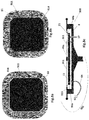
- the substrate carrier 813 can hold four substrates and the back plate assembly 602 ′ below can be adapted to this modified geometry, in particular having a multiplicity of compensating electrodes 16 beneath the multiplicity of substrate.
- the substrate carrier 813 comprises an electrically conductive material and is configured so that it can be electrically connected with the second electrode 8 when the substrate carrier 813 is positioned in the vacuum chamber 30 .
- the substrate carrier 813 illustrated in FIG. 7 a is shown to hold four substrates 811 , such as four wafers.
- the substrate carrier 813 is configured to be removable from the vacuum chamber 30 , to allow the substrates 811 to be mounted on the substrate carrier 813 .
- the substrate carrier 813 holds each of the substrates 811 such that at least the majority of an upper 40 a and opposite, lower surface 40 b , of each substrate 811 are untouched by the substrate carrier 813 or any other part of the plasma reactor 100 .
- FIG. 7 the substrate carrier 813 illustrated in FIG.
- the substrate carrier 813 comprises a four cut-out portions 814 each of which preferably have an area which is greater than the area of a substrate 811 and which can receive a substrate 811 .
- the manner in which each of the substrates 811 are held in a cut-out portion 814 is similar to what was described for an individual substrate in FIG. 3 , with supports having contact with the substrate only at the very edge where the device to be deposited is not active.
- the substrate carrier 813 comprises support members 813 a , 813 b which extend into the cut-out portions 814 .
- the substrates 811 rests on these support members 813 a , 813 b ; the length of the support members 813 a , 813 b is such that they extend along non-active parts 811 a , 811 b of each substrate 811 only. Thus an active parts 811 c of each substrate 811 remains untouched by the support members 813 a , 813 b or any other part of the plasma reactor 800 .
- the substrate carrier 813 will not comprise support members 813 a , 813 b and the cut-out portions 814 may each have an area which is slightly less than the area of a substrate 811 so that each substrate can rest directly on the substrate carrier 813 above a corresponding cut-out portion 814 . Again, in this case it is most preferable that substrate carrier 813 contacts only the non-active parts 811 a , 811 b of each substrate 811 .
- the corresponding back plate assembly 602 ′ further comprises four third electrodes 816 , corresponding to the four cut-out portions 814 provided in the substrate carrier 813 .
- Each of the four third electrodes 816 is electrically connected to a compensating device.
- Each of the four third electrodes 816 is positioned between the substrate carrier 813 and the second electrode 8 and the substrate carrier 813 may be arranged such that each of its cut-out portions 814 are aligned over a corresponding third electrode 816 .
- each substrate 811 held by the substrate carrier 813 can be aligned over a corresponding third electrode 816 .
- each of the third electrodes 816 are positioned such that there is a first clearance gap 12 between each third electrode 816 and substrate 811 .
- the first clearance gap 12 ensures that each substrate 811 is untouched by its corresponding third electrode 816 .
- the first clearance gap 12 between each substrate 811 and its corresponding third electrode 816 is about 1 mm.
- the second electrode 8 further comprises a post 25 ′ located towards the centre of the second electrode 8 .
- a center of the substrate carrier 813 will rest on the post 25 ′.
- the post 25 ′ will provide structural support to substrate carrier 813 so as to prevent the substrate 811 from warping under its own weight This ensures that a uniform distance between each of the substrates 811 and its corresponding third electrodes 816 is maintained.
- substrate carrier 813 is shown comprising four cut-out portions 814 and corresponding four third electrodes 816 , it should be understood that the substrate carrier 813 may comprise any number of cut-out portions 814 and corresponding any number of third electrodes 816 .
- FIG. 7 c illustrates a simpler design for a carrier accepting a multiplicity of substrates.
- the third electrode 16 is a single monolithic plate covering the ensemble of the substrate area and the adjacent parts of the substrate carrier such as 13 a and 13 b .
- This design is preferable for its simplicity as long as the planarity of the substrate carrier 13 can be preserved.
- FIG. 8 c illustrate a cross section view of plasma reactor vessel 900 in which has a substrate carrier 913 which comprises four cut-out portions 914 each of which can receive a substrate.
- the reactor vessel 900 comprises a single third electrode 916 which is large enough to extend beneath all four of the cut-out portions 914 .
- the single third electrode 916 is electrically connected to a compensating device 18 . This design is sufficient if the mechanical flatness of both carrier 913 and back plate assembly 902 are sufficient to guaranty a good control of the first clearance gap 12 beneath all the substrates 811 .
- Installing and running a plasma process requires changing the gas pressure inside the plasma reactor vessel, first installing the process pressure, then pumping out at the end of the process.
- the pressure changes there is a danger that a transient pressure differential develops between upper and lower surfaces of substrate(s); the transient pressure differential can lead to distortion of a very thin substrate.
- the substrate may warp to the extent that it touches a third electrode in the plasma reactor vessel. Or it may break. It is therefore desirable to limit the pressure differential between the upper and lower surfaces of the substrates.
- the area of the cut-out portion 914 in the substrate carrier 913 is configured to be larger than substrate 911 , a gap 62 is provided between the periphery of each substrate 911 and the part of the substrate carrier 813 which define the cut-out portion.
- area of the cut-out portion 914 is such that the gap 62 is equal to or less than 1 mm, preferably around 0.8 mm. The gap 62 will permit gas to pass between the volumes in plasma vessel reactor facing the upper and lower surfaces of the substrate. Thus, there will be no pressure differential between the areas in plasma vessel reactor in which the upper and lower surfaces occupy.
- the substrate carrier 913 comprises a cut-out portion which does not provide sufficient communication for gas at the periphery of substrate 911 .
- the substrate carrier 913 comprise a plurality of holes 61 which allow gas to pass through the substrate carrier 913 and thus allow gas exchange between the areas in plasma vessel reactor in which the upper and lower surfaces occupy.
- the diameter of each of the holes is less than 1 mm.
- more than thirty holes 61 are provided in the substrate carrier 913 .
- the volume behind the substrate enclose in assembly 902 and covered by the carrier 913 and the substrate(s) 911 form a close volume in diffusive communication with the activated gases from the plasma volume 30 .
- the ambient gas may contain unstable species leading to secondary contamination by the gas phase of the lower surface of the substrate; this may occur commonly in the doped layer deposition processes.
- a conduit 64 may be provided which is arranged to provide a flow of inactive gas across the lower surface 40 b of the substrate(s), as shown in FIG. 8 c .
- the conduit 64 is passed through the second electrode 8 .
- a gas supply 63 is connected to the conduit 64 , and it provides inactive gas which flows through the conduit, and across the lower surface 40 b of the substrate(s). The flow of inactive gas will limit the accumulation of process gas on the lower surface 40 b of the substrate(s) and will also rinse the area below the lower surface 40 b.
- the flow of inactive gas over the lower surface 40 b of the substrate(s) is only needed when the processing atmosphere within the plasma reactor vessel is baring a risk of spurious deposition which would lead to secondary contamination of the lower surface 40 b of the substrate(s) (as it would be the case during PECVD process with Boron hydrides).
- the plasma reactor vessel may not require a gas supply 63 and conduit 64 , instead the plasma volume 821 may either stay in static volume or allowed to communicate with the outer vacuum volume 30 .
- FIG. 9 illustrates an example of an assembly according to the present invention; the assembly defines a production line which comprises four vacuum vessels 1000 a - d .
- a substrate 1011 is transported successively to each of the four plasma reactive vessels 1000 a - d .
- Two of the vessels are represented equipped with PECVD reactors, the vessel 1000 a with a reactor coating the substrate downward, the next vessel 1000 c with a reactor coating the other face of the substrate, namely upward.
- the substrate 1011 is transported successively to each of the vessels 1000 a - d according to arrows 100 ab - bc - cd , by means of a carriage or some other suitable automatic transporting means.
- the reactor 1000 c has a configuration which is the inverse of the configuration of the preceding plasma reactive vessel 1000 b .
- the second and third electrodes 8 , 16 are located below the lower surface 40 b of the substrate 1011 and the first electrode 2 is located above the upper surface 40 a of the substrate 1011 .
- the second and third electrodes 8 , 16 are located above the upper surface 40 a of the substrate 1011 and the first electrode 2 is located below the lower surface 40 b of the substrate 1011 .
- plasma deposition will take place on the upper surface 40 a in the first plasma reactive vessel 1000 a in the production line; on the lower surface 40 b in the second plasma reactive vessel 1000 b in the production line; on the upper surface 40 a in the third plasma reactive vessel 1000 c in the production line; and finally on the lower surface 40 b in the fourth plasma reactive vessel 1000 d in the production line.
- a first substrate 10011 is seen pre-positioned in the reactor of chamber 1000 b , while the preceding substrate in the coating production sequence is seen prepositioned in the next chamber 1000 c.
- the assembly is not limited to the exemplary configuration of FIG. 9 but can further comprises any combination of vessels such as to be able to perform any arbitrary sequence of processes.
- the assembly can comprise a number of vessels different from four.
- the plurality of vessels can be arranged so that the substrate 1011 , when transported from a vessel to another, can be processed in any possible combination of process steps.
- the substrate 1011 can be processed sequentially upwardly and downwardly, several times upwardly (or downwardly) and then downwardly (or upwardly).
- the substrate 1011 can be transported successively to the successive process modules including the plasma reactive vessels 1000 b - c which are represented equipped with PECVD reactors, the vessel 1000 b with a reactor coating the substrate downward, the next vessel 1000 c with a reactor coating the other face of the substrate, namely upward.
- the substrate 1011 is transported successively to each of the vessels 1000 a - d by means of a carriage or some other suitable automatic transporting means.
- the plurality of vessels can also be arranged such that the combination of process steps comprises a combination of PECVD process steps and other process steps such as load-lock, heating, cooling, substrate flipping, plasma etching, plasma cleaning and PVD deposition such as evaporation or sputtering and reactive sputtering.
- each of the plasma reactive vessels 1000 a - d may have all the same configuration, and a means for flipping the substrate 1011 may be provided.
- the means for flipping the substrate 1011 will be operated to flip the substrate 1011 between successive plasma reactive vessels 1000 a - d so that plasma deposition can take place on the upper and lower surfaces 40 a , 40 b of the substrate 1011 successively, at each plasma reactive vessels 1000 a - d along the production line.
- each of the four plasma reactive vessels 1000 a - d by means of vacuum passages, along which the substrate 1011 can be passed. That way the substrate can be maintained in a vacuum environment as it is passed between the four plasma reactive vessels 1000 a - d .
- the substrate or the set of substrates
- the substrate will be held in a single substrate carrier 1013 and that substrate carrier, which holds the substrate 1011 , will be passed to the four reactive vessels 1000 a - d successively.
- the concept of the present invention is addressing specific devices where both sides of a substrate should contribute to the activity of a photo-electronic device.
- the present invention could be used in the manufacture of hetero-junction cells, or in the manufacture of power rectifiers.
Abstract
Description
V eff /V RF =e s/(e s +e g) (1),
where es is an equivalent thickness of the
L 2=2e s e g/[ε0 ωR □(e s +e g)] (2)
V eff=(V RF −V c)e s/(e s +e g) Eq. (3).
By choosing a suitable value for Vc the effective voltage Veff can be made equal to VRF. The suitable value for Vc which ensure that the effective voltage Veff is equal to VRF can be determined as:
V c=−(e g /e s)V RF Equation (4),
wherein eg is the
The minus sign indicates that the phase will be opposite to the one of VRF.
L(C g +C b)
Claims (11)
Applications Claiming Priority (4)
| Application Number | Priority Date | Filing Date | Title |
|---|---|---|---|
| EP13186529.7A EP2854155B1 (en) | 2013-09-27 | 2013-09-27 | Plasma reactor vessel and assembly, and a method of performing plasma processing |
| EP13186529 | 2013-09-27 | ||
| EP13186529.7 | 2013-09-27 | ||
| PCT/EP2014/070542 WO2015044295A1 (en) | 2013-09-27 | 2014-09-25 | Plasma reactor vessel and assembly, and a method of performing plasma processing |
Publications (2)
| Publication Number | Publication Date |
|---|---|
| US20160196959A1 US20160196959A1 (en) | 2016-07-07 |
| US10658159B2 true US10658159B2 (en) | 2020-05-19 |
Family
ID=49237126
Family Applications (1)
| Application Number | Title | Priority Date | Filing Date |
|---|---|---|---|
| US14/916,214 Active 2037-07-07 US10658159B2 (en) | 2013-09-27 | 2014-09-25 | Plasma reactor vessel having improved plasma uniformity comprised of a first electrode, a second electrode opposed to the first electrode, and a third electrode between a substrate carrier and the second electrode |
Country Status (8)
| Country | Link |
|---|---|
| US (1) | US10658159B2 (en) |
| EP (1) | EP2854155B1 (en) |
| JP (1) | JP6433502B2 (en) |
| KR (1) | KR102100315B1 (en) |
| CN (1) | CN105593968B (en) |
| HK (1) | HK1222475A1 (en) |
| MY (1) | MY178798A (en) |
| WO (1) | WO2015044295A1 (en) |
Families Citing this family (1)
| Publication number | Priority date | Publication date | Assignee | Title |
|---|---|---|---|---|
| US20210391146A1 (en) * | 2020-06-11 | 2021-12-16 | Applied Materials, Inc. | Rf frequency control and ground path return in semiconductor process chambers |
Citations (11)
| Publication number | Priority date | Publication date | Assignee | Title |
|---|---|---|---|---|
| US4969676A (en) | 1989-06-23 | 1990-11-13 | At&T Bell Laboratories | Air pressure pick-up tool |
| US5066340A (en) | 1989-08-09 | 1991-11-19 | Sanyo Electric Co., Ltd. | Photovoltaic device |
| US5981899A (en) * | 1997-01-17 | 1999-11-09 | Balzers Aktiengesellschaft | Capacitively coupled RF-plasma reactor |
| US6095084A (en) * | 1996-02-02 | 2000-08-01 | Applied Materials, Inc. | High density plasma process chamber |
| US6207890B1 (en) | 1997-03-21 | 2001-03-27 | Sanyo Electric Co., Ltd. | Photovoltaic element and method for manufacture thereof |
| KR20080020722A (en) | 2006-08-24 | 2008-03-06 | 세메스 주식회사 | Plasma processing apparatus and method for treating substrates using the same |
| US20080061041A1 (en) * | 2006-09-12 | 2008-03-13 | Seiko Epson Corporation | Plasma treatment apparatus and plasma treatment method |
| US20090294062A1 (en) * | 2008-05-29 | 2009-12-03 | Applied Materials, Inc. | Plasma reactor with plasma load impedance tuning for engineered transients by synchronized modulation of a source power or bias power rf generator |
| US20100282709A1 (en) | 2009-05-07 | 2010-11-11 | Samsung Mobile Display Co., Ltd. | Substrate plasma-processing apparatus |
| EP2333814A2 (en) | 2009-12-10 | 2011-06-15 | Orbotech LT Solar, LLC | Auto-sequencing multi-directional inline processing apparatus |
| US20130112546A1 (en) | 2011-11-04 | 2013-05-09 | Intevac, Inc. | Linear scanning sputtering system and method |
Family Cites Families (14)
| Publication number | Priority date | Publication date | Assignee | Title |
|---|---|---|---|---|
| DE69225002T2 (en) * | 1992-12-30 | 1998-09-03 | N Proizv Predprijatie Novatech | PLANT FOR VACUUM-PLASMA TREATMENT OF WORKPIECES |
| JP3238082B2 (en) * | 1996-05-16 | 2001-12-10 | シャープ株式会社 | Electronic device manufacturing equipment |
| JP3402129B2 (en) * | 1997-07-10 | 2003-04-28 | 松下電器産業株式会社 | Substrate dry etching equipment |
| WO2002073654A1 (en) * | 2001-03-13 | 2002-09-19 | Applied Materials, Inc. | Plasma chamber support having dual electrodes |
| DE10261362B8 (en) * | 2002-12-30 | 2008-08-28 | Osram Opto Semiconductors Gmbh | Substrate holder |
| KR100897176B1 (en) * | 2005-07-20 | 2009-05-14 | 삼성모바일디스플레이주식회사 | Inductively Coupled Plasma Processing Apparatus |
| JP4756361B2 (en) * | 2006-07-10 | 2011-08-24 | 株式会社デンソー | Rotational force transmission device |
| JP5349341B2 (en) * | 2007-03-16 | 2013-11-20 | ソースル シーオー エルティディー | Plasma processing apparatus and plasma processing method |
| US20110049100A1 (en) * | 2008-01-16 | 2011-03-03 | Charm Engineering Co., Ltd. | Substrate holder, substrate supporting apparatus, substrate processing apparatus, and substrate processing method using the same |
| US9887069B2 (en) * | 2008-12-19 | 2018-02-06 | Lam Research Corporation | Controlling ion energy distribution in plasma processing systems |
| JP5563347B2 (en) * | 2010-03-30 | 2014-07-30 | 東京エレクトロン株式会社 | Plasma processing apparatus and semiconductor device manufacturing method |
| JP5719599B2 (en) * | 2011-01-07 | 2015-05-20 | 東京エレクトロン株式会社 | Substrate processing equipment |
| JP5840095B2 (en) * | 2011-10-31 | 2016-01-06 | 三菱電機株式会社 | Solar cell manufacturing apparatus and solar cell manufacturing method |
| JP5996276B2 (en) * | 2012-05-31 | 2016-09-21 | 京セラ株式会社 | Electrostatic chuck, suction method and suction device |
-
2013
- 2013-09-27 EP EP13186529.7A patent/EP2854155B1/en active Active
-
2014
- 2014-09-25 MY MYPI2016000470A patent/MY178798A/en unknown
- 2014-09-25 KR KR1020167010241A patent/KR102100315B1/en active IP Right Grant
- 2014-09-25 CN CN201480052606.8A patent/CN105593968B/en active Active
- 2014-09-25 JP JP2016544755A patent/JP6433502B2/en active Active
- 2014-09-25 WO PCT/EP2014/070542 patent/WO2015044295A1/en active Application Filing
- 2014-09-25 US US14/916,214 patent/US10658159B2/en active Active
-
2016
- 2016-09-07 HK HK16110626.3A patent/HK1222475A1/en unknown
Patent Citations (11)
| Publication number | Priority date | Publication date | Assignee | Title |
|---|---|---|---|---|
| US4969676A (en) | 1989-06-23 | 1990-11-13 | At&T Bell Laboratories | Air pressure pick-up tool |
| US5066340A (en) | 1989-08-09 | 1991-11-19 | Sanyo Electric Co., Ltd. | Photovoltaic device |
| US6095084A (en) * | 1996-02-02 | 2000-08-01 | Applied Materials, Inc. | High density plasma process chamber |
| US5981899A (en) * | 1997-01-17 | 1999-11-09 | Balzers Aktiengesellschaft | Capacitively coupled RF-plasma reactor |
| US6207890B1 (en) | 1997-03-21 | 2001-03-27 | Sanyo Electric Co., Ltd. | Photovoltaic element and method for manufacture thereof |
| KR20080020722A (en) | 2006-08-24 | 2008-03-06 | 세메스 주식회사 | Plasma processing apparatus and method for treating substrates using the same |
| US20080061041A1 (en) * | 2006-09-12 | 2008-03-13 | Seiko Epson Corporation | Plasma treatment apparatus and plasma treatment method |
| US20090294062A1 (en) * | 2008-05-29 | 2009-12-03 | Applied Materials, Inc. | Plasma reactor with plasma load impedance tuning for engineered transients by synchronized modulation of a source power or bias power rf generator |
| US20100282709A1 (en) | 2009-05-07 | 2010-11-11 | Samsung Mobile Display Co., Ltd. | Substrate plasma-processing apparatus |
| EP2333814A2 (en) | 2009-12-10 | 2011-06-15 | Orbotech LT Solar, LLC | Auto-sequencing multi-directional inline processing apparatus |
| US20130112546A1 (en) | 2011-11-04 | 2013-05-09 | Intevac, Inc. | Linear scanning sputtering system and method |
Non-Patent Citations (1)
| Title |
|---|
| International Search Report and Written Opinion for PCT/EP2014/070542, dated Nov. 3, 2014, 12 pages. |
Also Published As
| Publication number | Publication date |
|---|---|
| JP2016541101A (en) | 2016-12-28 |
| CN105593968B (en) | 2017-10-27 |
| US20160196959A1 (en) | 2016-07-07 |
| EP2854155B1 (en) | 2017-11-08 |
| KR102100315B1 (en) | 2020-04-14 |
| KR20160058894A (en) | 2016-05-25 |
| WO2015044295A1 (en) | 2015-04-02 |
| CN105593968A (en) | 2016-05-18 |
| MY178798A (en) | 2020-10-20 |
| EP2854155A1 (en) | 2015-04-01 |
| JP6433502B2 (en) | 2018-12-05 |
| HK1222475A1 (en) | 2017-06-30 |
Similar Documents
| Publication | Publication Date | Title |
|---|---|---|
| TWI559425B (en) | Vertically integrated processing chamber | |
| TWI584409B (en) | Portable electrostatic chuck carrier for thin substrates | |
| KR101593460B1 (en) | Ground return for plasma processes | |
| US20100323113A1 (en) | Method to Synthesize Graphene | |
| EP2518763B1 (en) | A grounding assembly for vacuum processing apparatus | |
| US9011634B2 (en) | Plasma processing apparatus and plasma processing method | |
| US20210151302A1 (en) | Device for transporting a substrate, treatment device with a receiving plate adapted to a substrate carrier of a device of this kind, and method for processing a substrate using a device of this kind for the transport of a substrate, and treatment facility | |
| TW202102066A (en) | Ground strap assemblies | |
| US8395250B2 (en) | Plasma processing apparatus with an exhaust port above the substrate | |
| US10658159B2 (en) | Plasma reactor vessel having improved plasma uniformity comprised of a first electrode, a second electrode opposed to the first electrode, and a third electrode between a substrate carrier and the second electrode | |
| TWI455192B (en) | Prevention of film deposition on pecvd process chamber wall | |
| KR20190005929A (en) | Method and apparatus for vacuum processing | |
| CN113966543B (en) | Ground strap design | |
| JPH08260149A (en) | Reduced pressure surface treating device and apparatus for producing solar battery | |
| US20190382891A1 (en) | Method and solution for resolving cgt mura issue |
Legal Events
| Date | Code | Title | Description |
|---|---|---|---|
| AS | Assignment |
Owner name: INDEOTEC SA, SWITZERLAND Free format text: ASSIGNMENT OF ASSIGNORS INTEREST;ASSIGNORS:SHOJAEI, OMID REZA;SCHMITT, JACQUES;JEANNERET, FABRICE;SIGNING DATES FROM 20160216 TO 20160218;REEL/FRAME:037889/0802 |
|
| STPP | Information on status: patent application and granting procedure in general |
Free format text: NON FINAL ACTION MAILED |
|
| STPP | Information on status: patent application and granting procedure in general |
Free format text: RESPONSE TO NON-FINAL OFFICE ACTION ENTERED AND FORWARDED TO EXAMINER |
|
| STPP | Information on status: patent application and granting procedure in general |
Free format text: FINAL REJECTION MAILED |
|
| STPP | Information on status: patent application and granting procedure in general |
Free format text: DOCKETED NEW CASE - READY FOR EXAMINATION |
|
| FEPP | Fee payment procedure |
Free format text: ENTITY STATUS SET TO UNDISCOUNTED (ORIGINAL EVENT CODE: BIG.); ENTITY STATUS OF PATENT OWNER: LARGE ENTITY |
|
| STPP | Information on status: patent application and granting procedure in general |
Free format text: PUBLICATIONS -- ISSUE FEE PAYMENT VERIFIED |
|
| STCF | Information on status: patent grant |
Free format text: PATENTED CASE |
|
| MAFP | Maintenance fee payment |
Free format text: PAYMENT OF MAINTENANCE FEE, 4TH YEAR, LARGE ENTITY (ORIGINAL EVENT CODE: M1551); ENTITY STATUS OF PATENT OWNER: LARGE ENTITY Year of fee payment: 4 |