US10652486B2 - Image sensor with electron and hole collection electrodes - Google Patents
Image sensor with electron and hole collection electrodes Download PDFInfo
- Publication number
- US10652486B2 US10652486B2 US16/341,898 US201716341898A US10652486B2 US 10652486 B2 US10652486 B2 US 10652486B2 US 201716341898 A US201716341898 A US 201716341898A US 10652486 B2 US10652486 B2 US 10652486B2
- Authority
- US
- United States
- Prior art keywords
- collecting electrode
- pixel
- holes
- electrons
- electron
- Prior art date
- Legal status (The legal status is an assumption and is not a legal conclusion. Google has not performed a legal analysis and makes no representation as to the accuracy of the status listed.)
- Active
Links
- 238000003384 imaging method Methods 0.000 claims abstract description 9
- 239000000758 substrate Substances 0.000 claims abstract description 9
- 239000004065 semiconductor Substances 0.000 claims abstract description 8
- 238000006243 chemical reaction Methods 0.000 claims description 22
- 238000000034 method Methods 0.000 claims description 12
- 230000008878 coupling Effects 0.000 claims description 2
- 238000010168 coupling process Methods 0.000 claims description 2
- 238000005859 coupling reaction Methods 0.000 claims description 2
- 238000012546 transfer Methods 0.000 description 10
- 239000003990 capacitor Substances 0.000 description 9
- 238000010586 diagram Methods 0.000 description 8
- 230000000875 corresponding effect Effects 0.000 description 6
- 238000012545 processing Methods 0.000 description 4
- VYPSYNLAJGMNEJ-UHFFFAOYSA-N Silicium dioxide Chemical compound O=[Si]=O VYPSYNLAJGMNEJ-UHFFFAOYSA-N 0.000 description 2
- XUIMIQQOPSSXEZ-UHFFFAOYSA-N Silicon Chemical compound [Si] XUIMIQQOPSSXEZ-UHFFFAOYSA-N 0.000 description 2
- 238000003491 array Methods 0.000 description 2
- 239000002800 charge carrier Substances 0.000 description 2
- 230000002596 correlated effect Effects 0.000 description 2
- 230000003287 optical effect Effects 0.000 description 2
- 238000005070 sampling Methods 0.000 description 2
- 229910052710 silicon Inorganic materials 0.000 description 2
- 239000010703 silicon Substances 0.000 description 2
- 101100365736 Candida albicans (strain SC5314 / ATCC MYA-2876) SEP7 gene Proteins 0.000 description 1
- RYGMFSIKBFXOCR-UHFFFAOYSA-N Copper Chemical compound [Cu] RYGMFSIKBFXOCR-UHFFFAOYSA-N 0.000 description 1
- 101100175606 Oryza sativa subsp. japonica AGPL2 gene Proteins 0.000 description 1
- 101150070874 SHR1 gene Proteins 0.000 description 1
- 101150009276 SHR2 gene Proteins 0.000 description 1
- 101150105385 SHS1 gene Proteins 0.000 description 1
- 229910052782 aluminium Inorganic materials 0.000 description 1
- XAGFODPZIPBFFR-UHFFFAOYSA-N aluminium Chemical compound [Al] XAGFODPZIPBFFR-UHFFFAOYSA-N 0.000 description 1
- 239000000872 buffer Substances 0.000 description 1
- 229910052681 coesite Inorganic materials 0.000 description 1
- 230000000295 complement effect Effects 0.000 description 1
- 229910052802 copper Inorganic materials 0.000 description 1
- 239000010949 copper Substances 0.000 description 1
- 229910052906 cristobalite Inorganic materials 0.000 description 1
- 230000003247 decreasing effect Effects 0.000 description 1
- 239000006185 dispersion Substances 0.000 description 1
- 230000002708 enhancing effect Effects 0.000 description 1
- 239000000463 material Substances 0.000 description 1
- 229910052751 metal Inorganic materials 0.000 description 1
- 239000002184 metal Substances 0.000 description 1
- 229910044991 metal oxide Inorganic materials 0.000 description 1
- 150000004706 metal oxides Chemical class 0.000 description 1
- 238000012986 modification Methods 0.000 description 1
- 230000004048 modification Effects 0.000 description 1
- 230000005693 optoelectronics Effects 0.000 description 1
- 239000002096 quantum dot Substances 0.000 description 1
- 229920006395 saturated elastomer Polymers 0.000 description 1
- 239000000377 silicon dioxide Substances 0.000 description 1
- 230000006641 stabilisation Effects 0.000 description 1
- 238000011105 stabilization Methods 0.000 description 1
- 229910052682 stishovite Inorganic materials 0.000 description 1
- 229910052905 tridymite Inorganic materials 0.000 description 1
Images


Classifications
-
- H—ELECTRICITY
- H04—ELECTRIC COMMUNICATION TECHNIQUE
- H04N—PICTORIAL COMMUNICATION, e.g. TELEVISION
- H04N25/00—Circuitry of solid-state image sensors [SSIS]; Control thereof
- H04N25/50—Control of the SSIS exposure
- H04N25/57—Control of the dynamic range
-
- H04N5/355—
-
- H—ELECTRICITY
- H01—ELECTRIC ELEMENTS
- H01L—SEMICONDUCTOR DEVICES NOT COVERED BY CLASS H10
- H01L27/00—Devices consisting of a plurality of semiconductor or other solid-state components formed in or on a common substrate
- H01L27/14—Devices consisting of a plurality of semiconductor or other solid-state components formed in or on a common substrate including semiconductor components sensitive to infrared radiation, light, electromagnetic radiation of shorter wavelength or corpuscular radiation and specially adapted either for the conversion of the energy of such radiation into electrical energy or for the control of electrical energy by such radiation
- H01L27/144—Devices controlled by radiation
- H01L27/146—Imager structures
- H01L27/14601—Structural or functional details thereof
- H01L27/14603—Special geometry or disposition of pixel-elements, address-lines or gate-electrodes
-
- H—ELECTRICITY
- H01—ELECTRIC ELEMENTS
- H01L—SEMICONDUCTOR DEVICES NOT COVERED BY CLASS H10
- H01L27/00—Devices consisting of a plurality of semiconductor or other solid-state components formed in or on a common substrate
- H01L27/14—Devices consisting of a plurality of semiconductor or other solid-state components formed in or on a common substrate including semiconductor components sensitive to infrared radiation, light, electromagnetic radiation of shorter wavelength or corpuscular radiation and specially adapted either for the conversion of the energy of such radiation into electrical energy or for the control of electrical energy by such radiation
- H01L27/144—Devices controlled by radiation
- H01L27/146—Imager structures
- H01L27/14601—Structural or functional details thereof
- H01L27/14609—Pixel-elements with integrated switching, control, storage or amplification elements
-
- H—ELECTRICITY
- H01—ELECTRIC ELEMENTS
- H01L—SEMICONDUCTOR DEVICES NOT COVERED BY CLASS H10
- H01L27/00—Devices consisting of a plurality of semiconductor or other solid-state components formed in or on a common substrate
- H01L27/14—Devices consisting of a plurality of semiconductor or other solid-state components formed in or on a common substrate including semiconductor components sensitive to infrared radiation, light, electromagnetic radiation of shorter wavelength or corpuscular radiation and specially adapted either for the conversion of the energy of such radiation into electrical energy or for the control of electrical energy by such radiation
- H01L27/144—Devices controlled by radiation
- H01L27/146—Imager structures
- H01L27/14643—Photodiode arrays; MOS imagers
-
- H—ELECTRICITY
- H01—ELECTRIC ELEMENTS
- H01L—SEMICONDUCTOR DEVICES NOT COVERED BY CLASS H10
- H01L27/00—Devices consisting of a plurality of semiconductor or other solid-state components formed in or on a common substrate
- H01L27/14—Devices consisting of a plurality of semiconductor or other solid-state components formed in or on a common substrate including semiconductor components sensitive to infrared radiation, light, electromagnetic radiation of shorter wavelength or corpuscular radiation and specially adapted either for the conversion of the energy of such radiation into electrical energy or for the control of electrical energy by such radiation
- H01L27/144—Devices controlled by radiation
- H01L27/146—Imager structures
- H01L27/14665—Imagers using a photoconductor layer
Definitions
- the present invention relates generally to image sensing devices, and particularly to circuits and methods for enhancing the performance of film-based image sensors.
- a silicon-based switching array is overlaid with a photosensitive film such as a film containing a dispersion of quantum dots. Films of this sort are referred to as “quantum films.”
- the switching array which can be similar to those used in complementary metal-oxide sandwich (CMOS) image sensors that are known in the art, is coupled by suitable electrodes to the film in order to read out the photocharge that accumulates in each pixel of the film due to incident light.
- CMOS complementary metal-oxide sandwich
- Embodiments of the present invention that are described hereinbelow provide enhanced image sensor designs and methods for operation of image sensors with enhanced performance.
- imaging apparatus including a photosensitive medium configured to convert incident photons into pairs of electrons and holes.
- An array of pixel circuits is formed on a semiconductor substrate.
- Each pixel circuit defining a respective pixel and includes an electron-collecting electrode in contact with the photosensitive medium at a first location in the pixel and a hole-collecting electrode in contact with the photosensitive medium at a second location in the pixel.
- the pixel circuits include circuitry coupled to apply a positive potential to and collect the electrons from the electron-collecting electrode and to apply a negative potential to and collect the holes from the hole-collecting electrode and to output a signal indicative of an intensity of the incident photons responsively to the collected electrons and holes.
- the photosensitive medium includes a quantum film.
- the apparatus includes a common electrode, which is at least partially transparent, overlying the photosensitive medium and is biased at a voltage between the positive potential applied to the electron-collecting electrode and the negative potential applied to the hole-collecting electrode.
- the electron-collecting electrode and the hole-collecting electrode extend through the photosensitive medium.
- the circuitry in each pixel circuit includes a first charge store coupled to collect the electrons from the electron-collecting electrode and a second charge store coupled to collect the holes from the hole-collecting electrode and is configured to output the signal as a differential output between the first and second charge stores.
- the circuitry is configured to collect the holes with a first conversion gain and to collect the electrons with a second conversion gain, which is different from the first conversion gain, and to output the signal with a dynamic range that is enhanced responsively to a relation between the first and second conversion gains.
- the apparatus includes a column circuit, which is configured to generate a first digital signal corresponding to the collected electrons and a second digital signal corresponding to the collected holes, and to select one of the first and second digital signals to produce a digital output signal with the enhanced dynamic range.
- a method for imaging which includes coupling an array of pixel circuits formed on a semiconductor substrate to a photosensitive medium configured to convert incident photons into pairs of electrons and holes.
- Each pixel circuit defines a respective pixel and includes an electron-collecting electrode in contact with the photosensitive medium at a first location in the pixel and a hole-collecting electrode in contact with the photosensitive medium at a second location in the pixel.
- a positive potential is applied in each pixel to the electron-collecting electrode and a negative potential is applied to the hole-collecting electrode.
- the electrons are collected from the electron-collecting electrode and the holes from the hole-collecting electrode, and a signal is output indicative of an intensity of the incident photons responsively to the collected electrons and holes.
- FIG. 1 is a schematic side view of a camera module, which is operative in accordance with an embodiment of the invention
- FIG. 2 is a schematic top view of an example image sensor, in accordance with an embodiment of the invention.
- FIG. 3 is a schematic sectional illustration of a pixel in an image sensor, in accordance with an embodiment of the invention.
- FIG. 4 is a plot that schematically illustrates the electrical potential distribution in a quantum film along two vertical section lines in FIG. 3 , in accordance with an embodiment of the invention
- FIG. 5 is a schematic sectional illustration of a pixel in an image sensor, in accordance with an alternative embodiment of the invention.
- FIGS. 6 and 7 are schematic top views of image sensing arrays, in accordance with embodiments of the invention.
- FIG. 8 is an electrical circuit diagram, which schematically illustrates elements of a pixel circuit, in accordance with an embodiment of the invention.
- FIG. 9 is a signal timing diagram that schematically illustrates signals in the pixel circuit of FIG. 8 , in accordance with an embodiment of the invention.
- FIG. 10 is an electrical circuit diagram, which schematically illustrates elements of pixel readout circuitry, in accordance with an embodiment of the invention.
- FIG. 11 is a signal timing diagram that schematically illustrates signals used in reading out accumulated charge in the circuitry of FIG. 10 , in accordance with an embodiment of the invention.
- FIG. 1 shows one example of a camera module 100 that may utilize an image sensor 102 , which may be configured in any manner as described below.
- the camera module 100 may comprise a lens system 104 , which may direct and focus incoming light onto image sensor 102 . While depicted in FIG. 1 as a single element, it should be appreciated that lens system 104 may actually include a plurality of lens elements, some or all of which may be fixed relative to each other (e.g., via a lens barrel or the like).
- the camera module 102 may optionally be configured to move the lens system 104 and/or the image sensor 102 to perform autofocus and/or optical image stabilization.
- the camera module may further comprise one or more optional filters, such as a filter 106 , which may be placed along the optical path.
- Filter 106 may reflect or otherwise block certain wavelengths of light, and may substantially prevent, based on the effectiveness of the filter, these wavelengths of light from reaching the image sensor 102 .
- filter 106 may comprise an infrared cutoff filter. While shown in FIG. 1 as being positioned between image sensor 102 and lens system 104 , filter 106 may be positioned to cover lens system 104 (relative to incoming light) or may be positioned between lenses of lens system 104 .
- FIG. 2 shows a top view of an exemplary image sensor 200 as described herein.
- Image sensor 200 may comprise an imaging area comprising a pixel array 202 , which may include a first plurality of pixels 212 that may be used to convert incident light into electrical signals.
- pixel array 202 may comprise an obscured region 210 including at least one pixel (e.g., a second plurality of pixels) that is obscured relative to incoming light (e.g., covered by a light-blocking layer). Electrical signals may still be read out from some or all of these pixels, but since there is ideally no light reaching these pixels, the current measured from these pixels may represent the dark current associated with one or more components of the image sensor.
- Image sensor 200 (or associated processing circuitry) may compensate for the dark current levels during image capture and/or processing.
- Image sensor 200 may further comprise row circuitry 204 and column circuitry 206 , which collectively may be used to convey various signals (e.g., bias voltages, reset signals) to individual pixels as well as to read out signals from individual pixels.
- row circuitry 204 may be configured to simultaneously control multiple pixels in a given row
- column circuitry 206 may convey pixel electrical signals to other circuitry for processing.
- image sensor 200 may comprise control circuitry 208 , which may control the row circuitry 204 and column circuitry 206 , as well as performing input/output operations (e.g., parallel or serial IO operations) for image sensor 200 .
- the control circuitry may include a combination of analog circuits (e.g., circuits to provide bias and reference levels) and digital circuits (e.g., image enhancement circuitry, line buffers to temporarily store lines of pixel values, register banks that control global device operation and/or frame format).
- analog circuits e.g., circuits to provide bias and reference levels
- digital circuits e.g., image enhancement circuitry, line buffers to temporarily store lines of pixel values, register banks that control global device operation and/or frame format.
- FIG. 3 is a schematic sectional illustration of a pixel 300 in an image sensor, such as image sensor 200 , in accordance with an embodiment of the invention.
- Pixel 300 shows a single example, which is typically replicated over the entire array of pixels in the image sensor.
- Pixel 300 comprises a photosensitive medium, such as a quantum film 302 , which converts incident photons into pairs of electrons (e) and holes (h).
- An array of pixel circuits 304 formed on a semiconductor substrate 305 , such as a silicon wafer, defines an array of pixels in film 302 .
- Pixel circuit 304 comprises an electron-collecting electrode 306 and a hole-collecting electrode 308 in contact with film 302 at different, respective locations in pixel 300 . Electrodes 306 and 308 may be surrounded by an insulating layer 309 , such as a layer of SiO 2 .
- This pixel configuration differs from image sensors that are known in the art, in which only electrons or only holes are collected, while the other type of charge carriers (holes or electrons, as the case may be) are drained into the power supply. Separate collection of both types of charge carriers, as provided by embodiments of the present invention, enables pixel 300 to sense incident light intensity with enhanced signal/noise ratio and dynamic range.
- Pixel circuit 304 further comprises circuitry coupled to apply a positive potential to and collect the electrons from electron-collecting electrode 306 via a sense node (SN 1 ) 310 , and to apply a negative potential to and collect the holes from hole-collecting electrode 308 via a sense node (SN 2 ) 312 .
- the sense nodes and associated circuitry are typically formed on substrate 305 , for example by a CMOS process.
- an additional common electrode 314 which is at least partially transparent, overlies film 302 and is biased at a voltage between the positive potential applied to electron-collecting electrode 306 and the negative potential applied to hole-collecting electrode 308 .
- Sense nodes 310 and 312 serve as charge stores for the collected electrons and holes, respectively. Based on the electrons and holes collected at sense nodes 310 and 312 , pixel circuit 304 outputs a signal indicative of the intensity of the incident photons on film 302 in pixel 300 .
- the terms “positive” and “negative” in reference to the potentials applied to electrodes 306 and 308 are used in a relative sense, i.e., “positive” simply means higher than some baseline, while “negative” means lower than the baseline.
- the baseline voltage may be, for instance, the bias that is applied to common electrode 314 , as illustrated in the example shown in FIG. 4 .
- FIG. 4 is a plot that schematically illustrates the electrical potential distribution in quantum film 302 along two vertical section lines in FIG. 3 , in accordance with an embodiment of the invention.
- a curve 402 shows the potential distribution along line A-A, above electron-collection electrode 306 ; while a curve 404 shows the potential distribution along line B-B, above hole-collecting electrode 308 .
- a bias of 1 volt is applied to hole-collection electrode 308 ; a bias of 2 volts is applied to common electrode 314 ; and a bias of 4 volts is applied to electron-collection electrode 306 .
- FIG. 5 is a schematic sectional illustration of a pixel 500 in an image sensor, in accordance with an alternative embodiment of the invention.
- Pixel 500 is similar in structure and operation to pixel 300 , as described above, and elements of pixel 500 are labeled with the same reference numbers as corresponding elements of pixel 300 .
- Pixel 500 differs from the preceding embodiment, however, in that an electron-collection electrode 502 and a hole-collection electrode 504 extend upward through quantum film 302 .
- Electrodes 502 and 504 may be formed, for example, by buildup of copper or aluminum dividers above the sorts of electrodes that are shown in FIG. 3 . These dividers are useful in avoiding “dead zones” and crosstalk between pixels that could otherwise occur at the top of quantum film 302 , where the electrical potential drops (as can be seen at the right side of FIG. 4 ).
- FIGS. 6 and 7 are schematic top views of image sensing arrays 600 and 700 , made up of pixels 300 and 500 , respectively, in accordance with embodiments of the invention. Each drawing includes four neighboring pixels. Electrodes 306 and 308 , which contact the bottom side of film 302 , are shown in FIG. 6 by dashed lines. FIG. 7 shows electrodes 502 and 504 , which extend through to the top of film 302 .
- FIG. 8 is an electrical circuit diagram, which schematically illustrates elements of a pixel circuit 800 , in accordance with an embodiment of the invention.
- Circuit 800 can be used in pixel 300 , as a part of pixel circuit 304 , or in pixel 500 , and outputs a differential signal output based on the charges stored by sense nodes 310 and 312 , due to collected electrons and holes, respectively.
- pixel circuit 800 comprises an electron readout circuit 802 and a hole readout circuit 804 , which are coupled across a differential read bus 807 .
- Circuits 802 and 804 comprise respective reset transistors 803 and 805 and source-follower transistors 806 and 808 .
- the reset voltage V RST1 for electron readout circuit 802 is low, while the reset voltage V RST2 for hole readout circuit 804 is high.
- Pixel readout starts when respective select transistors 810 and 812 are switched on, thus connecting source-follower transistors 806 and 808 to read bus 807 .
- the resulting differential output has a signal level twice that of a single-ended readout, as well as inherent cancellation of row noise.
- FIG. 9 is a signal timing diagram that schematically illustrates signals in pixel circuit 800 , in accordance with an embodiment of the invention.
- Pixel readout begins when a select signal 900 to transistors 810 and 812 goes high, thus switching on the transistors.
- Read bus 807 now receives signals 904 and 906 from sense nodes 310 and 312 , giving a differential readout on the bus equal to the sum of the individual amplitudes of signals 904 and 906 .
- a reset pulse 902 is applied to transistors 803 and 805 , causing the level of signal 904 to drop and that of signal 906 to increase.
- Bus 807 outputs the differential signal level after the reset pulse.
- the row noise appears as a common-mode signal and is thus rejected by the differential readout.
- the levels of signals 904 and 906 may once again grow as further electrons and holes accumulate, as illustrated by the dashed lines at the right side of the figure.
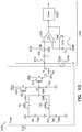
- FIG. 10 is an electrical circuit diagram, which schematically illustrates elements of pixel readout circuitry 1000 , in accordance with an alternative embodiment of the invention.
- Circuitry 1000 comprises a pixel circuit 1002 , which can be used in pixel 300 , as a part of pixel circuit 304 , or in pixel 500 , to output a signal with extended dynamic range.
- the signal is read out and digitized by a column circuit 1004 , which in this implementation includes a dual-slope analog-to-digital converter (ADC).
- ADC analog-to-digital converter
- sense nodes 310 (SN 1 ) and 312 (SN 2 ) are assumed to have different conversion gains.
- SN 1 as the electron collection node, may have high conversion gain
- SN 2 as the hole collection node
- the conversion gains depend on the equivalent capacitances of the sense nodes and may be adjusted by increasing or decreasing the respective capacitance.
- Circuitry 1000 outputs a signal that is indicative of the intensity of light that is incident on the pixel, with a dynamic range that is enhanced by a factor based on the relation (ratio or difference) between the first and second conversion gains.
- column circuit 1004 generates a first digital input signal corresponding to the electrons collected by sense node 310 and a second digital input signal corresponding to the holes collected by sense node 312 .
- the digital input signals can be output selectively, using the high-gain signal when incident light intensity is low and the low-gain signal when incident light intensity is high, causing the high-gain signal to saturate.
- Column circuit 1004 thus produces a digital output signal with enhanced dynamic range. Details of this process are described below.
- Pixel circuit 1002 comprises transfer gates (T 1 , T 2 ) 1003 and 1006 , which are respectively coupled between sense nodes 310 and 312 and an FD node 1008 .
- a reset transistor (T 3 ) 1010 resets node 1008 to the reset voltage V RST .
- a source follower transistor (T 4 ) 1012 and row select transistor (T 5 ) 1014 couple FD node 1008 to a column input 1016 .
- Column circuit 1004 comprises a source follower current source (I VLN ) 1018 and a comparator 1020 .
- Column input 1016 is coupled to the positive input of comparator 1020 via a capacitor C 1
- a ramp input is coupled to the negative input of the comparator via a capacitor C 2 .
- the inputs to comparator 1020 are controlled by a correlated double-sampling (CDS) switch 1022 (SW 1 ) and an auto-zero (AZ) switch 1024 (SW 2 ).
- CDS correlated double-sampling
- AZ auto-zero
- the output of the comparator drives a latch 1026 , which captures a digital value corresponding to the time at which the ramp voltage on the negative input to the comparator is equal to the voltage at column input 1016 .
- FIG. 11 is a signal timing diagram that schematically illustrates signals used in reading out the accumulated charge from pixel circuit 1002 via column circuit 1004 , in accordance with an embodiment of the invention.
- Readout starts with assertion of a select (SEL) signal 1100 to a high level on row select transistor 1014 , thus connecting source follower transistor 1012 to column input 1016 .
- a reset voltage (V RST ) 1102 is held initially at a high level V RST1 .
- Applying a reset signal 1104 to reset transistor 1010 resets FD node 1008 to the high voltage level V RST1 , as shown by an FD signal 1114 .
- This reference level of FD signal 1114 is labeled “SHR 1 .”
- Transfer signals 1106 (TX 1 ) and 1108 (TX 2 ) remain low, so that transfer gates 1003 and 1006 are closed.
- a CDS signal 1110 and an AZ signal 1112 are applied to switches 1022 and 1024 , respectively.
- the left plate of capacitor C 1 is thus charged to the high reset level V RST1 , while the right plate of capacitor C 1 is charged to VCDS, as is the top plate of capacitor C 2 .
- Switches 1022 and 1024 are then opened before signal transfer, causing the inputs to comparator 1020 to float.
- Transfer signal 1106 (TX 1 ) is now asserted high, and the electron signal charge is transferred from sense node 310 via transfer gate 1003 into FD node 1008 .
- V RST1 is set to a level much higher than the potential under transfer gate 1003 , so that there is no charge sharing between sense node 310 and FD node 1008 .
- FD signal 1114 accordingly drops to the electron signal level marked “SHS 1 ” in FIG. 11 .
- the positive input of comparator 1020 senses the difference between the previous reset and the current signal level and converts the difference to a digital value on the downward ramp of the ramp signal applied to capacitor C 2 .
- reset signal 1104 to reset transistor 1010 is again set high, while transfer gate 1003 remains open. This reset will resolve any overflow at FD node 1008 .
- the kTC noise at sense node 310 can be reduced by a soft reset of the sense node, while the kTC noise at FD node 1008 is cancelled by correlated double-sampling.
- the hole signal charge at sense node 312 (SN 2 ) is read out in similar fashion.
- FD node 1008 is reset to the low voltage level V RST2 , giving the low reference value “SHR 2 ” of FD signal 1114 .
- CDS and AZ signals 1110 and 1112 are asserted as in the first phase.
- the left plate of capacitor C 1 is thus charged to the low reset level, after which the FD signal goes up after charge transfer through transfer gate 1006 , giving the hole signal level “SHS 2 .”
- ADC conversion is done in this phase on the upward ramp. Subsequent processing can use the resulting hole signal level if the electron signal level is saturated.
- Dynamic range extension is determined by the ratio of the electron and hole conversion gains.
- C SN2 is determined by the pixel size and the dielectric constant of the capacitor.
- a metal-insulator-metal (MIM) capacitor can have a capacitance up to 18 fF/ ⁇ m 2 when a high-K dielectric is used.
- a pixel with a pitch of 2 ⁇ m can have C SN2 of about 18 fF, which is equivalent a capacity of 125K electrons (assuming 1V swing at pixel output) and 83 dB dynamic range.
Abstract
Description
N ns=√(k*T*C FD), (1)
wherein k is Boltzmann's constant and T is temperature. The kTC noise at
CGH =q/C FD, (2)
wherein q is the elementary charge. The row conversion gain is given by:
CGL =q/(C SN2 +C FD) (3)
The pixel dynamic range is then given by:
DR=20*log(N max /N sn) (4)
wherein Nmax is the maximum electron charge capacity and Nsn is the noise electron charge. Assuming dV=1 volt swing at the pixel output, Nmax is given by:
N max =dV/CGH=1/CGH (5)
Nsn can be nine electrons for CFD=0.5 fF.
Claims (12)
Priority Applications (1)
| Application Number | Priority Date | Filing Date | Title |
|---|---|---|---|
| US16/341,898 US10652486B2 (en) | 2016-10-20 | 2017-10-19 | Image sensor with electron and hole collection electrodes |
Applications Claiming Priority (3)
| Application Number | Priority Date | Filing Date | Title |
|---|---|---|---|
| US201662410795P | 2016-10-20 | 2016-10-20 | |
| PCT/US2017/057283 WO2018075705A1 (en) | 2016-10-20 | 2017-10-19 | Image sensor with electron and hole collection electrodes |
| US16/341,898 US10652486B2 (en) | 2016-10-20 | 2017-10-19 | Image sensor with electron and hole collection electrodes |
Publications (2)
| Publication Number | Publication Date |
|---|---|
| US20190246051A1 US20190246051A1 (en) | 2019-08-08 |
| US10652486B2 true US10652486B2 (en) | 2020-05-12 |
Family
ID=60263024
Family Applications (1)
| Application Number | Title | Priority Date | Filing Date |
|---|---|---|---|
| US16/341,898 Active US10652486B2 (en) | 2016-10-20 | 2017-10-19 | Image sensor with electron and hole collection electrodes |
Country Status (3)
| Country | Link |
|---|---|
| US (1) | US10652486B2 (en) |
| CN (1) | CN109863603B (en) |
| WO (1) | WO2018075705A1 (en) |
Cited By (1)
| Publication number | Priority date | Publication date | Assignee | Title |
|---|---|---|---|---|
| US10998371B1 (en) * | 2018-08-20 | 2021-05-04 | Apple Inc. | Film-based image sensor with suppressed light reflection and flare artifact |
Families Citing this family (1)
| Publication number | Priority date | Publication date | Assignee | Title |
|---|---|---|---|---|
| FR3085246B1 (en) * | 2018-08-23 | 2020-09-18 | St Microelectronics Crolles 2 Sas | BUILT-IN IMAGE SENSOR WITH GLOBAL SHUTTER SUITABLE FOR THE ACHIEVEMENT OF LARGE DYNAMIC RANGE IMAGES |
Citations (19)
| Publication number | Priority date | Publication date | Assignee | Title |
|---|---|---|---|---|
| US5683595A (en) | 1995-03-31 | 1997-11-04 | Shimadzu Corporation | Fine pattern forming method and fine pattern device |
| US5889313A (en) | 1996-02-08 | 1999-03-30 | University Of Hawaii | Three-dimensional architecture for solid state radiation detectors |
| US6026964A (en) | 1997-08-25 | 2000-02-22 | International Business Machines Corporation | Active pixel sensor cell and method of using |
| WO2003067663A1 (en) | 2002-02-08 | 2003-08-14 | Qinetiq Limited | Photodetector circuit |
| US6943409B1 (en) | 2004-05-24 | 2005-09-13 | International Business Machines Corporation | Trench optical device |
| US20070029581A1 (en) * | 2005-08-08 | 2007-02-08 | International Business Machines Corporation | Pixel sensor cell for collecting electrons and holes |
| WO2007102051A2 (en) | 2005-08-25 | 2007-09-13 | Edward Sargent | Quantum dot optical devices with enhanced gain and sensitivity and methods of making same |
| US7470965B2 (en) | 2003-09-11 | 2008-12-30 | Panasonic Corporation | Solid-state imaging device |
| WO2009071587A2 (en) | 2007-12-04 | 2009-06-11 | Teknoflow Oy | Back-thinned radiation detector with '3d' active region and corresponding methods of manufacturing and use |
| US20100038523A1 (en) | 2008-02-12 | 2010-02-18 | Omnivision Technologies, Inc. | Image sensor with buried self aligned focusing element |
| US7923801B2 (en) | 2007-04-18 | 2011-04-12 | Invisage Technologies, Inc. | Materials, systems and methods for optoelectronic devices |
| US20110226934A1 (en) | 2010-03-19 | 2011-09-22 | Hui Tian | Image sensors employing sensitized semiconductor diodes |
| US8120028B2 (en) | 2006-04-25 | 2012-02-21 | Au Optronics Corporation | Active device array substrate, color filter substrate and manufacturing methods thereof |
| US8222709B2 (en) | 2005-10-28 | 2012-07-17 | Sony Corporation | Solid-state imaging device, method of driving solid-state imaging device and imaging apparatus |
| US8304707B2 (en) | 2005-08-24 | 2012-11-06 | Aptina Imaging Corporation | Method and apparatus providing an optical guide in image sensor devices |
| US8354693B2 (en) | 2007-06-07 | 2013-01-15 | Panasonic Corporation | Solid state imaging device and method for fabricating the same |
| US8704281B2 (en) | 2009-08-28 | 2014-04-22 | Fujifilm Corporation | Process of making a solid state imaging device |
| US9941316B2 (en) | 2014-06-10 | 2018-04-10 | Invisage Technologies, Inc. | Multi-terminal optoelectronic devices for light detection |
| US9972652B2 (en) | 2010-06-08 | 2018-05-15 | Invisage Technologies, Inc. | Photodetector comprising a pinned photodiode that is formed by an optically sensitive layer and a silicon diode |
Family Cites Families (1)
| Publication number | Priority date | Publication date | Assignee | Title |
|---|---|---|---|---|
| US9602750B2 (en) * | 2014-11-25 | 2017-03-21 | Semiconductor Components Industries, Llc | Image sensor pixels having built-in variable gain feedback amplifier circuitry |
-
2017
- 2017-10-19 US US16/341,898 patent/US10652486B2/en active Active
- 2017-10-19 WO PCT/US2017/057283 patent/WO2018075705A1/en active Application Filing
- 2017-10-19 CN CN201780064716.XA patent/CN109863603B/en active Active
Patent Citations (21)
| Publication number | Priority date | Publication date | Assignee | Title |
|---|---|---|---|---|
| US5683595A (en) | 1995-03-31 | 1997-11-04 | Shimadzu Corporation | Fine pattern forming method and fine pattern device |
| US5889313A (en) | 1996-02-08 | 1999-03-30 | University Of Hawaii | Three-dimensional architecture for solid state radiation detectors |
| US6026964A (en) | 1997-08-25 | 2000-02-22 | International Business Machines Corporation | Active pixel sensor cell and method of using |
| WO2003067663A1 (en) | 2002-02-08 | 2003-08-14 | Qinetiq Limited | Photodetector circuit |
| US7470965B2 (en) | 2003-09-11 | 2008-12-30 | Panasonic Corporation | Solid-state imaging device |
| US6943409B1 (en) | 2004-05-24 | 2005-09-13 | International Business Machines Corporation | Trench optical device |
| US20070029581A1 (en) * | 2005-08-08 | 2007-02-08 | International Business Machines Corporation | Pixel sensor cell for collecting electrons and holes |
| US8304707B2 (en) | 2005-08-24 | 2012-11-06 | Aptina Imaging Corporation | Method and apparatus providing an optical guide in image sensor devices |
| WO2007102051A2 (en) | 2005-08-25 | 2007-09-13 | Edward Sargent | Quantum dot optical devices with enhanced gain and sensitivity and methods of making same |
| US8222709B2 (en) | 2005-10-28 | 2012-07-17 | Sony Corporation | Solid-state imaging device, method of driving solid-state imaging device and imaging apparatus |
| US8120028B2 (en) | 2006-04-25 | 2012-02-21 | Au Optronics Corporation | Active device array substrate, color filter substrate and manufacturing methods thereof |
| US7923801B2 (en) | 2007-04-18 | 2011-04-12 | Invisage Technologies, Inc. | Materials, systems and methods for optoelectronic devices |
| US8354693B2 (en) | 2007-06-07 | 2013-01-15 | Panasonic Corporation | Solid state imaging device and method for fabricating the same |
| WO2009071587A2 (en) | 2007-12-04 | 2009-06-11 | Teknoflow Oy | Back-thinned radiation detector with '3d' active region and corresponding methods of manufacturing and use |
| US20100038523A1 (en) | 2008-02-12 | 2010-02-18 | Omnivision Technologies, Inc. | Image sensor with buried self aligned focusing element |
| US8704281B2 (en) | 2009-08-28 | 2014-04-22 | Fujifilm Corporation | Process of making a solid state imaging device |
| US20110226934A1 (en) | 2010-03-19 | 2011-09-22 | Hui Tian | Image sensors employing sensitized semiconductor diodes |
| US8822897B2 (en) * | 2010-03-19 | 2014-09-02 | Invisage Technologies, Inc. | Image sensors employing sensitized semiconductor diodes |
| US9972653B2 (en) | 2010-03-19 | 2018-05-15 | Invisage Technologies, Inc. | Image sensors employing sensitized semiconductor diodes |
| US9972652B2 (en) | 2010-06-08 | 2018-05-15 | Invisage Technologies, Inc. | Photodetector comprising a pinned photodiode that is formed by an optically sensitive layer and a silicon diode |
| US9941316B2 (en) | 2014-06-10 | 2018-04-10 | Invisage Technologies, Inc. | Multi-terminal optoelectronic devices for light detection |
Non-Patent Citations (4)
| Title |
|---|
| International Application PCT/US2017/057283 Search report dated Jan. 31, 2018. |
| Nishimura et al., "An Over 120dB Simultaneous-Capture Wide-Dynamic-Range 1.6e-Ultra-Low-Reset-Noise Organic-Photoconductive-Film CMOS Image Sensor", IEEE International Solid-State Circuits Conference (ISSCC'16), session 6, pp. 110-111, year 2016. |
| Nishimura et al., "An Over 120dB Simultaneous-Capture Wide-Dynamic-Range 1.6e—Ultra-Low-Reset-Noise Organic-Photoconductive-Film CMOS Image Sensor", IEEE International Solid-State Circuits Conference (ISSCC'16), session 6, pp. 110-111, year 2016. |
| U.S. Appl. No. 15/939,331 office action dated May 24, 2019. |
Cited By (1)
| Publication number | Priority date | Publication date | Assignee | Title |
|---|---|---|---|---|
| US10998371B1 (en) * | 2018-08-20 | 2021-05-04 | Apple Inc. | Film-based image sensor with suppressed light reflection and flare artifact |
Also Published As
| Publication number | Publication date |
|---|---|
| CN109863603B (en) | 2023-02-17 |
| CN109863603A (en) | 2019-06-07 |
| WO2018075705A1 (en) | 2018-04-26 |
| US20190246051A1 (en) | 2019-08-08 |
Similar Documents
| Publication | Publication Date | Title |
|---|---|---|
| KR100834424B1 (en) | Image sensor | |
| US9531976B2 (en) | Systems and methods for operating image sensor pixels having different sensitivities and shared charge storage regions | |
| RU2589489C2 (en) | Image forming apparatus, image forming system and method for actuation of image forming apparatus | |
| EP3008756B1 (en) | Split-gate conditional- reset image sensor | |
| US11303857B2 (en) | Imaging device including pixel array and addition circuit | |
| US7626620B2 (en) | Photoelectric conversion unit stacked structure | |
| JP4804254B2 (en) | Photoelectric conversion device and imaging device | |
| US10154210B2 (en) | Global shutter imaging pixels | |
| JP2016201649A (en) | Imaging apparatus, imaging system, and driving method for imaging apparatus | |
| EP2517461B1 (en) | Column output circuits for image sensors | |
| CN113382188A (en) | Optical detection device | |
| CN111430388A (en) | Imaging pixel | |
| JP2017103514A (en) | Solid state image pickup device and imaging system | |
| JP7116599B2 (en) | Imaging device, semiconductor device and camera | |
| US9608025B2 (en) | Imaging apparatus and imaging system | |
| US10791294B2 (en) | Image sensors having capacitively coupled pixels | |
| US20190280031A1 (en) | Dual conversion gain circuitry with buried channels | |
| US10075663B2 (en) | Phase detection pixels with high speed readout | |
| CN112449135A (en) | Imaging system with adjustable amplifier circuit | |
| CN212811862U (en) | Image sensor with a plurality of pixels | |
| US10652486B2 (en) | Image sensor with electron and hole collection electrodes | |
| US10771723B2 (en) | Systems and methods for voltage settling | |
| RU2688953C1 (en) | Device for reading signals from a photodetector matrix of infrared radiation (versions) | |
| US10785426B2 (en) | Apparatus and methods for generating high dynamic range images | |
| JP5019655B2 (en) | Photoelectric conversion device and imaging device |
Legal Events
| Date | Code | Title | Description |
|---|---|---|---|
| FEPP | Fee payment procedure |
Free format text: ENTITY STATUS SET TO UNDISCOUNTED (ORIGINAL EVENT CODE: BIG.); ENTITY STATUS OF PATENT OWNER: LARGE ENTITY |
|
| AS | Assignment |
Owner name: INVISAGE TECHNOLOGIES, INC., CALIFORNIA Free format text: ASSIGNMENT OF ASSIGNORS INTEREST;ASSIGNORS:MANDELLI, EMANUELE;BEILEY, ZACHARY M.;BOCK, NIKOLAI E.;SIGNING DATES FROM 20190403 TO 20190408;REEL/FRAME:048879/0786 |
|
| STPP | Information on status: patent application and granting procedure in general |
Free format text: DOCKETED NEW CASE - READY FOR EXAMINATION |
|
| STPP | Information on status: patent application and granting procedure in general |
Free format text: NON FINAL ACTION MAILED |
|
| STPP | Information on status: patent application and granting procedure in general |
Free format text: RESPONSE TO NON-FINAL OFFICE ACTION ENTERED AND FORWARDED TO EXAMINER |
|
| STPP | Information on status: patent application and granting procedure in general |
Free format text: NOTICE OF ALLOWANCE MAILED -- APPLICATION RECEIVED IN OFFICE OF PUBLICATIONS |
|
| STCF | Information on status: patent grant |
Free format text: PATENTED CASE |
|
| MAFP | Maintenance fee payment |
Free format text: PAYMENT OF MAINTENANCE FEE, 4TH YEAR, LARGE ENTITY (ORIGINAL EVENT CODE: M1551); ENTITY STATUS OF PATENT OWNER: LARGE ENTITY Year of fee payment: 4 |