US10641699B2 - Method of making a carrier for molecular detection - Google Patents
Method of making a carrier for molecular detection Download PDFInfo
- Publication number
- US10641699B2 US10641699B2 US16/119,663 US201816119663A US10641699B2 US 10641699 B2 US10641699 B2 US 10641699B2 US 201816119663 A US201816119663 A US 201816119663A US 10641699 B2 US10641699 B2 US 10641699B2
- Authority
- US
- United States
- Prior art keywords
- carbon nanotube
- nanometers
- composite structure
- strip
- metal layer
- Prior art date
- Legal status (The legal status is an assumption and is not a legal conclusion. Google has not performed a legal analysis and makes no representation as to the accuracy of the status listed.)
- Active
Links
Images


Classifications
-
- G—PHYSICS
- G01—MEASURING; TESTING
- G01N—INVESTIGATING OR ANALYSING MATERIALS BY DETERMINING THEIR CHEMICAL OR PHYSICAL PROPERTIES
- G01N15/00—Investigating characteristics of particles; Investigating permeability, pore-volume, or surface-area of porous materials
- G01N15/10—Investigating individual particles
- G01N15/14—Electro-optical investigation, e.g. flow cytometers
- G01N15/1484—Electro-optical investigation, e.g. flow cytometers microstructural devices
-
- C—CHEMISTRY; METALLURGY
- C23—COATING METALLIC MATERIAL; COATING MATERIAL WITH METALLIC MATERIAL; CHEMICAL SURFACE TREATMENT; DIFFUSION TREATMENT OF METALLIC MATERIAL; COATING BY VACUUM EVAPORATION, BY SPUTTERING, BY ION IMPLANTATION OR BY CHEMICAL VAPOUR DEPOSITION, IN GENERAL; INHIBITING CORROSION OF METALLIC MATERIAL OR INCRUSTATION IN GENERAL
- C23C—COATING METALLIC MATERIAL; COATING MATERIAL WITH METALLIC MATERIAL; SURFACE TREATMENT OF METALLIC MATERIAL BY DIFFUSION INTO THE SURFACE, BY CHEMICAL CONVERSION OR SUBSTITUTION; COATING BY VACUUM EVAPORATION, BY SPUTTERING, BY ION IMPLANTATION OR BY CHEMICAL VAPOUR DEPOSITION, IN GENERAL
- C23C14/00—Coating by vacuum evaporation, by sputtering or by ion implantation of the coating forming material
- C23C14/02—Pretreatment of the material to be coated
- C23C14/021—Cleaning or etching treatments
-
- C—CHEMISTRY; METALLURGY
- C23—COATING METALLIC MATERIAL; COATING MATERIAL WITH METALLIC MATERIAL; CHEMICAL SURFACE TREATMENT; DIFFUSION TREATMENT OF METALLIC MATERIAL; COATING BY VACUUM EVAPORATION, BY SPUTTERING, BY ION IMPLANTATION OR BY CHEMICAL VAPOUR DEPOSITION, IN GENERAL; INHIBITING CORROSION OF METALLIC MATERIAL OR INCRUSTATION IN GENERAL
- C23C—COATING METALLIC MATERIAL; COATING MATERIAL WITH METALLIC MATERIAL; SURFACE TREATMENT OF METALLIC MATERIAL BY DIFFUSION INTO THE SURFACE, BY CHEMICAL CONVERSION OR SUBSTITUTION; COATING BY VACUUM EVAPORATION, BY SPUTTERING, BY ION IMPLANTATION OR BY CHEMICAL VAPOUR DEPOSITION, IN GENERAL
- C23C14/00—Coating by vacuum evaporation, by sputtering or by ion implantation of the coating forming material
- C23C14/04—Coating on selected surface areas, e.g. using masks
- C23C14/042—Coating on selected surface areas, e.g. using masks using masks
-
- C—CHEMISTRY; METALLURGY
- C23—COATING METALLIC MATERIAL; COATING MATERIAL WITH METALLIC MATERIAL; CHEMICAL SURFACE TREATMENT; DIFFUSION TREATMENT OF METALLIC MATERIAL; COATING BY VACUUM EVAPORATION, BY SPUTTERING, BY ION IMPLANTATION OR BY CHEMICAL VAPOUR DEPOSITION, IN GENERAL; INHIBITING CORROSION OF METALLIC MATERIAL OR INCRUSTATION IN GENERAL
- C23C—COATING METALLIC MATERIAL; COATING MATERIAL WITH METALLIC MATERIAL; SURFACE TREATMENT OF METALLIC MATERIAL BY DIFFUSION INTO THE SURFACE, BY CHEMICAL CONVERSION OR SUBSTITUTION; COATING BY VACUUM EVAPORATION, BY SPUTTERING, BY ION IMPLANTATION OR BY CHEMICAL VAPOUR DEPOSITION, IN GENERAL
- C23C14/00—Coating by vacuum evaporation, by sputtering or by ion implantation of the coating forming material
- C23C14/06—Coating by vacuum evaporation, by sputtering or by ion implantation of the coating forming material characterised by the coating material
- C23C14/14—Metallic material, boron or silicon
-
- C—CHEMISTRY; METALLURGY
- C23—COATING METALLIC MATERIAL; COATING MATERIAL WITH METALLIC MATERIAL; CHEMICAL SURFACE TREATMENT; DIFFUSION TREATMENT OF METALLIC MATERIAL; COATING BY VACUUM EVAPORATION, BY SPUTTERING, BY ION IMPLANTATION OR BY CHEMICAL VAPOUR DEPOSITION, IN GENERAL; INHIBITING CORROSION OF METALLIC MATERIAL OR INCRUSTATION IN GENERAL
- C23C—COATING METALLIC MATERIAL; COATING MATERIAL WITH METALLIC MATERIAL; SURFACE TREATMENT OF METALLIC MATERIAL BY DIFFUSION INTO THE SURFACE, BY CHEMICAL CONVERSION OR SUBSTITUTION; COATING BY VACUUM EVAPORATION, BY SPUTTERING, BY ION IMPLANTATION OR BY CHEMICAL VAPOUR DEPOSITION, IN GENERAL
- C23C16/00—Chemical coating by decomposition of gaseous compounds, without leaving reaction products of surface material in the coating, i.e. chemical vapour deposition [CVD] processes
- C23C16/02—Pretreatment of the material to be coated
- C23C16/0227—Pretreatment of the material to be coated by cleaning or etching
- C23C16/0245—Pretreatment of the material to be coated by cleaning or etching by etching with a plasma
-
- C—CHEMISTRY; METALLURGY
- C23—COATING METALLIC MATERIAL; COATING MATERIAL WITH METALLIC MATERIAL; CHEMICAL SURFACE TREATMENT; DIFFUSION TREATMENT OF METALLIC MATERIAL; COATING BY VACUUM EVAPORATION, BY SPUTTERING, BY ION IMPLANTATION OR BY CHEMICAL VAPOUR DEPOSITION, IN GENERAL; INHIBITING CORROSION OF METALLIC MATERIAL OR INCRUSTATION IN GENERAL
- C23C—COATING METALLIC MATERIAL; COATING MATERIAL WITH METALLIC MATERIAL; SURFACE TREATMENT OF METALLIC MATERIAL BY DIFFUSION INTO THE SURFACE, BY CHEMICAL CONVERSION OR SUBSTITUTION; COATING BY VACUUM EVAPORATION, BY SPUTTERING, BY ION IMPLANTATION OR BY CHEMICAL VAPOUR DEPOSITION, IN GENERAL
- C23C16/00—Chemical coating by decomposition of gaseous compounds, without leaving reaction products of surface material in the coating, i.e. chemical vapour deposition [CVD] processes
- C23C16/04—Coating on selected surface areas, e.g. using masks
- C23C16/042—Coating on selected surface areas, e.g. using masks using masks
-
- C—CHEMISTRY; METALLURGY
- C23—COATING METALLIC MATERIAL; COATING MATERIAL WITH METALLIC MATERIAL; CHEMICAL SURFACE TREATMENT; DIFFUSION TREATMENT OF METALLIC MATERIAL; COATING BY VACUUM EVAPORATION, BY SPUTTERING, BY ION IMPLANTATION OR BY CHEMICAL VAPOUR DEPOSITION, IN GENERAL; INHIBITING CORROSION OF METALLIC MATERIAL OR INCRUSTATION IN GENERAL
- C23C—COATING METALLIC MATERIAL; COATING MATERIAL WITH METALLIC MATERIAL; SURFACE TREATMENT OF METALLIC MATERIAL BY DIFFUSION INTO THE SURFACE, BY CHEMICAL CONVERSION OR SUBSTITUTION; COATING BY VACUUM EVAPORATION, BY SPUTTERING, BY ION IMPLANTATION OR BY CHEMICAL VAPOUR DEPOSITION, IN GENERAL
- C23C16/00—Chemical coating by decomposition of gaseous compounds, without leaving reaction products of surface material in the coating, i.e. chemical vapour deposition [CVD] processes
- C23C16/06—Chemical coating by decomposition of gaseous compounds, without leaving reaction products of surface material in the coating, i.e. chemical vapour deposition [CVD] processes characterised by the deposition of metallic material
-
- G—PHYSICS
- G01—MEASURING; TESTING
- G01N—INVESTIGATING OR ANALYSING MATERIALS BY DETERMINING THEIR CHEMICAL OR PHYSICAL PROPERTIES
- G01N21/00—Investigating or analysing materials by the use of optical means, i.e. using sub-millimetre waves, infrared, visible or ultraviolet light
- G01N21/62—Systems in which the material investigated is excited whereby it emits light or causes a change in wavelength of the incident light
- G01N21/63—Systems in which the material investigated is excited whereby it emits light or causes a change in wavelength of the incident light optically excited
- G01N21/65—Raman scattering
- G01N2021/653—Coherent methods [CARS]
- G01N2021/655—Stimulated Raman
-
- G—PHYSICS
- G01—MEASURING; TESTING
- G01N—INVESTIGATING OR ANALYSING MATERIALS BY DETERMINING THEIR CHEMICAL OR PHYSICAL PROPERTIES
- G01N21/00—Investigating or analysing materials by the use of optical means, i.e. using sub-millimetre waves, infrared, visible or ultraviolet light
- G01N21/62—Systems in which the material investigated is excited whereby it emits light or causes a change in wavelength of the incident light
- G01N21/63—Systems in which the material investigated is excited whereby it emits light or causes a change in wavelength of the incident light optically excited
- G01N21/65—Raman scattering
- G01N21/658—Raman scattering enhancement Raman, e.g. surface plasmons
Definitions
- the subject matter herein generally relates to a method of making a carrier for molecule detection.
- Raman spectroscopy is widely used for use in single molecule detection.
- a method for detecting single molecules using Raman spectroscopy is provided.
- An aggregated silver particle film is coated on a surface of a glass substrate.
- a number of single molecule samples are disposed on the aggregated silver particle film.
- a laser irradiation is supplied to the single molecule samples by a Raman detection system to cause a Raman scattering and produce a Raman spectroscopy.
- the Raman spectroscopy is received by a sensor and analyzed by a computer.
- the substrate for carrying single molecules is usually rigid and made of rigid materials such as glass, silicon, silicon dioxide, silicon nitride, quartz, gallium nitride, alumina or magnesium oxide.
- the single molecules have to be extracted before the detecting from the object and the object with anomalistic shapes cannot be detected in real time, in situ, on line, or in vivo.
- FIG. 1 is a schematic view of a carrier for use in single molecule detection.
- FIG. 2 is a cross-sectional view, along a line II-II of FIG. 1 .
- FIG. 3 is a flow chart of a method for making carrier for the single molecule detection.
- FIG. 4 is a cross-sectional view, along a line IV-IV of FIG. 3 .
- FIG. 5 is a Scanning Electron Microscope (SEM) image of a drawn carbon nanotube film.
- FIG. 6 is an SEM image of an untwisted carbon nanotube wire.
- FIG. 7 is an SEM image of a twisted carbon nanotube wire.
- FIG. 8 is an SEM image of a carbon nanotube composite structure.
- FIG. 9 is an SEM image of a single carbon nanotube coated with an alumina (Al 2 O 3 ) layer.
- FIG. 10 is a flow chart of a method for detecting single molecules.
- FIG. 11 is a Raman spectroscopy of analytes with different concentrations measured from both sides of the carrier.
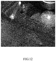
- FIG. 12 is a photo of detecting crystal violet (CV) molecules on a tomato's surface by Raman spectrometer in situ.
- FIG. 13 is a Raman spectroscopy of CV molecules on a tomato's surface.
- FIG. 14 is a Raman spectroscopy of 4-ATP molecule on the carrier after wiping the surface of apples with the carrier.
- FIG. 15 is a schematic view of a carrier for use in single molecule detection.
- FIG. 16 is a flow chart of a method for making carrier for the single molecule detection.
- FIG. 17 is a schematic view of a carrier for use in single molecule detection.
- FIG. 18 is a flow chart of a method for making carrier for the single molecule detection.
- FIG. 19 is a schematic view of a molecular detection device.
- FIG. 20 is a schematic view of a carrier supported by a metal frame.
- FIG. 21 is a schematic view of a plurality of carriers for use in single molecule detection.
- connection can be such that the objects are permanently connected or releasably connected.
- substantially is defined to be essentially conforming to the particular dimension, shape, or other feature that the term modifies, such that the component need not be exact.
- comprising means “including, but not necessarily limited to”; it specifically indicates open-ended inclusion or membership in a so-described combination, group, series, and the like. It should be noted that references to “an” or “one” embodiment in this disclosure are not necessarily to the same embodiment, and such references mean “at least one.”
- FIG. 1 and FIG. 2 show a carrier 10 for use in single molecule of an embodiment detection is provided.
- the carrier 10 comprises a substrate 11 , a middle layer 12 and a metal layer 13 .
- the middle layer 12 is on the substrate 11 surface, and the metal layer 13 is on the middle layer 12 surface.
- the middle layer 12 comprises a base 121 and a patterned bulge 122 on a surface of the base 121 away from the substrate 11 .
- the patterned bulge 122 comprises a plurality of strip-shaped bulges 125 intersecting with each other to form a net and defines a plurality of holes 124 .
- the plurality of strip-shaped bulges 125 is an integrated structure.
- the substrate 11 can be an insulating substrate or a semiconductor substrate.
- the substrate 11 is a flexible substrate.
- the substrate 11 can be placed on a curved surface to be coincident with the curved surface.
- the substrate 11 can be made of a material such as polyethylene terephthalate (PET), polyimide (PI), polymethylmethacrylate (PMMA), polydimethylsiloxane (PDMS), or polyethylene naphthalate (PEN).
- PET polyethylene terephthalate
- PI polyimide
- PMMA polymethylmethacrylate
- PDMS polydimethylsiloxane
- PEN polyethylene naphthalate
- the shape, size and thickness of the substrate 11 can be selected according to need. Since the substrate 11 of the carrier 10 is the flexible substrate and can fit on irregular surfaces, the carrier 10 can be used on irregular surfaces for molecular detection in situ.
- the material of the substrate 11 is PET, and the substrate 11 is a flat plate.
- the base 121 is on a surface of substrate 11 .
- the base 121 defines two surfaces, and the two surfaces are opposite.
- the patterned bulge 122 can be placed on a single surface or the two surfaces opposite to each other of the base 121 .
- the thickness of the base 121 ranges from 50 nanometers to 300 nanometers. In one embodiment, the thickness of the base 121 ranges from 100 nanometers to 200 nanometers. If the base 121 is too thin, for example, less than 100 nanometers, a Raman spectroscopy of analytes can be interfered by the substrate 11 or affected by the substrate 11 . If the base 121 is too thick, for example greater than 200 nanometers, the flexibility of the carrier 10 is reduced.
- the base 121 can be insulating material such as silicon dioxide, or silicon nitride.
- the base 121 can also comprise semiconductor materials such as gallium nitride, or gallium arsenide.
- the base 121 and the patterned bulge 122 can have the same material or different materials.
- the base 121 and the patterned bulge 122 are integrated structures, the material of the integrated structure is silicon dioxide.
- the patterned bulge 122 comprises the plurality of strip-shaped bulges 125 .
- the plurality of strip-shaped bulges 125 comprises a plurality of first strip-shaped bulges 126 and a plurality of second strip-shaped bulges 127 .
- the plurality of first strip-shaped bulges 126 are substantially parallel to each other and extends along a first direction
- the plurality of second strip-shaped bulges 127 are substantially parallel to each other and extend along a second direction, which is different from the first direction.
- the angle between the first direction and the second direction is greater than 0 degrees and less than or equal to 90 degrees. In one embodiment, the angle between the first direction and the second direction is greater than 30 degrees. In one embodiment, the angle between the first direction and the second direction is 90 degrees.
- Each of the plurality of strip-shaped bulges 125 has a length less than or equal to the width of length of the base 121 .
- the width of the plurality of strip-shaped bulges 125 can range from between about 20 nanometers to about 150 nanometers. In one embodiment, the width of the plurality of strip-shaped bulges 125 can be in a range from about 50 nanometers to about 100 nanometers. The height of the plurality of strip-shaped bulges 125 range from about 100 nanometers to 500 nanometers. In one embodiment, the height of the plurality of strip-shaped bulges 125 can range from about 200 nanometers to 400 nanometers. In one embodiment, the height of the plurality of strip-shaped bulges 125 is 300 nanometers. The distance between two adjacent strip-shaped bulges 125 can range from about 10 nanometers to about 300 nanometers.
- the distance between two adjacent strip-shaped bulges 125 can range from about 10 nanometers to about 50 nanometers.
- the average diameter of the plurality of holes 124 can range from about 10 nanometers to about 300 nanometers, and the depth of the plurality of holes 124 can range from about 100 nanometers to about 500 nanometers.
- the metal layer 13 is on surfaces of the patterned bulge 122 .
- the metal layer 13 can be a continuous structure.
- the metal layer 13 can be formed on both top and side surfaces of the plurality of strip-shaped bulges 125 and bottom surfaces of the plurality of holes 124 .
- the metal layer 13 can also be formed as a discontinuous structure.
- the metal layer 13 can be formed on side surfaces of the plurality of strip-shaped bulges 125 and bottom surfaces of the plurality of holes 124 .
- the metal layer 13 can be formed as a single-layer or a multi-layer structure.
- a surface plasmon resonance (SPR) is produced on a surface of the metal layer 13 so that the surface improved Raman scattering (SERS) of the carrier 10 will be outstandingly improved.
- the thickness of the metal layer 13 can range from about 2 nanometers to about 200 nanometers.
- the material of the metal layer 13 can be gold, silver, copper, platinum, iron, nickel, aluminum, or any alloy thereof.
- the metal layer 13 can be uniformly deposited on the surface of the substrate 11 by a method of electron beam evaporation, chemical vapor deposition (CVD), or sputtering.
- the metal layer 13 is a gold layer with a thickness of about 10 nanometers.
- FIGS. 3-4 show a method for making the carrier 10 of one embodiment. The method includes the following blocks:
- the material of the middle layer 12 can be insulating material or semiconductor material.
- the insulating material can be silicon dioxide or silicon nitride.
- the semiconductor material can be silicon, gallium nitride, or gallium arsenide.
- the middle layer 12 is placed on the substrate 11 surface and in direct contact with the substrate 11 surface. The method of depositing the middle layer 12 on the substrate 11 surface is not limited. In one embodiment, the middle layer 12 is deposited on the substrate 11 surface by plasma chemical vapor deposition.
- the carbon nanotube composite structure 110 includes a carbon nanotube structure 112 and a protective layer 114 coated on the carbon nanotube structure 112 .
- the carbon nanotube structure 112 is a free-standing structure.
- the carbon nanotube structure 112 can be suspended by two spaced supports.
- the plurality of carbon nanotubes can be single-walled carbon nanotubes, double-walled carbon nanotubes, or multi-walled carbon nanotubes.
- the length and diameter of the plurality of carbon nanotubes can be selected according to need.
- the diameter of the single-walled carbon nanotubes can range from about 0.5 nanometers to about 10 nanometers.
- the diameter of the double-walled carbon nanotubes can range from about 1.0 nanometer to about 15 nanometers.
- the diameter of the multi-walled carbon nanotubes can range from about 1.5 nanometers to about 50 nanometers.
- the length of the carbon nanotubes is greater than 50 micrometers. In one embodiment, the length of the carbon nanotubes can range from about 200 micrometers to about 900 micrometers.
- the carbon nanotubes are orderly arranged to form an ordered carbon nanotube structure.
- the plurality of carbon nanotubes extends along a direction substantially parallel to the surface of the carbon nanotube structure 112 .
- ordered carbon nanotube structure includes, but is not limited to, a structure wherein the plurality of carbon nanotubes are arranged approximately along the same direction.
- the carbon nanotube structure 112 defines a plurality of apertures.
- the aperture extends throughout the carbon nanotube structure 112 along a thickness direction thereof.
- the aperture can be a hole created by several adjacent carbon nanotubes, or a gap created by two substantially parallel carbon nanotubes and extending along an axial direction of the carbon nanotubes.
- the hole shaped aperture and the gap shaped aperture can exist in the carbon nanotube structure 112 simultaneously.
- the aperture sizes are referred as the diameter of the hole or width of the gap.
- the sizes of the apertures can be different.
- the average aperture sizes can range from about 1 nanometer to about 500 micrometers.
- the sizes of the apertures can be about 10 nanometers, 50 nanometers, 100 nanometers, 500 nanometers, 1 micrometer, 10 micrometers, 80 micrometers, or 120 micrometers.
- the carbon nanotube structure 112 includes at least one carbon nanotube film, at least one carbon nanotube wire, or combination thereof.
- the carbon nanotube structure 112 includes a single carbon nanotube film or two or more carbon nanotube films stacked together.
- the thickness of the carbon nanotube structure 112 can therefore be controlled by the number of the stacked carbon nanotube films.
- the number of the stacked carbon nanotube films can be in a range from about 2 to about 100.
- the number of the stacked carbon nanotube films can be 10, 30, or 50.
- the carbon nanotube structure 112 is formed by folding a single carbon nanotube wire.
- the carbon nanotube structure 112 may include a layer of carbon nanotube wires that are parallel and spaced from each other.
- the carbon nanotube structure 112 includes a plurality of carbon nanotube wires intersected or weaved together to form a carbon nanotube net.
- the distance between two adjacent parallel and spaced carbon nanotube wires can range from about 0.1 micrometers to about 200 micrometers. In one embodiment, the distance between two adjacent parallel and spaced carbon nanotube wires is in a range from about 10 micrometers to about 100 micrometers.
- the gap between two adjacent substantially parallel carbon nanotube wires is defined as the apertures.
- the size of the apertures can be controlled by controlling the distance between two adjacent parallel and spaced carbon nanotube wires.
- the length of the gap between two adjacent parallel carbon nanotube wires can be equal to the length of the carbon nanotube wire. Any carbon nanotube structure described herein can be used in all embodiments.
- the carbon nanotube structure 112 includes at least one drawn carbon nanotube film.
- the drawn carbon nanotube film can be drawn from a carbon nanotube array having a drawn film therefrom.
- the drawn carbon nanotube film includes a plurality of carbon nanotubes joined end-to-end by van der Waals attractive force therebetween.
- the drawn carbon nanotube film is a free-standing film.
- each drawn carbon nanotube film includes a plurality of successively oriented carbon nanotube segments joined end-to-end by van der Waals attractive force therebetween.
- Each carbon nanotube segment includes a plurality of carbon nanotubes parallel to each other, and combined by van der Waals attractive force therebetween. As shown in FIG. 5 , some variations can occur in the drawn carbon nanotube film.
- the carbon nanotubes in the drawn carbon nanotube film are oriented along a preferred orientation.
- the drawn carbon nanotube film can be treated with an organic solvent to increase the mechanical strength and toughness, and reduce the coefficient of friction of the drawn carbon nanotube film.
- a thickness of the drawn carbon nanotube film can range from about 0.5 nanometers to about 100 micrometers.
- the drawn carbon nanotube film defines a plurality of apertures between adjacent carbon nanotubes.
- the carbon nanotube structure 112 includes at least two stacked drawn carbon nanotube films. In other embodiments, the carbon nanotube structure 112 includes two or more coplanar carbon nanotube films, and further includes layers of coplanar carbon nanotube films. Additionally, when the carbon nanotubes in the carbon nanotube film are aligned along one preferred orientation (e.g., the drawn carbon nanotube film), the orientations of carbon nanotubes in adjacent films are different, an angle can exist between the orientations of carbon nanotubes in adjacent films, whether stacked or adjacent. Adjacent carbon nanotube films can be combined only by the van der Waals attractive force therebetween. An angle between the carbon nanotubes alignment directions in two adjacent carbon nanotube films can range from about 0 degrees to about 90 degrees.
- the carbon nanotube structure 112 When the angle between the carbon nanotubes alignment directions in adjacent stacked drawn carbon nanotube films is larger than 0 degrees, a plurality of micropores is defined by the carbon nanotube structure 112 .
- the carbon nanotube structure 112 has the carbon nanotubes alignment directions between adjacent stacked drawn carbon nanotube films at 90 degrees. Stacking the carbon nanotube films will also add to the structural integrity of the carbon nanotube structure 112 .
- the carbon nanotube wires can be untwisted or twisted. Treating the drawn carbon nanotube film with a volatile organic solvent can form the untwisted carbon nanotube wire. Specifically, the using organic solvent is used to soak the entire surface of the drawn carbon nanotube film. While soaking, adjacent parallel carbon nanotubes in the drawn carbon nanotube film will bundle together, due to the surface tension of the organic solvent as it volatilizes, and thus, the drawn carbon nanotube film will be shrunk into an untwisted carbon nanotube wire.
- FIG. 6 shows the untwisted carbon nanotube wire includes a plurality of carbon nanotubes substantially oriented along the same direction (i.e., a direction along the length of the untwisted carbon nanotube wire). The carbon nanotubes are substantially parallel to the axis of the untwisted carbon nanotube wire.
- the untwisted carbon nanotube wire includes a plurality of successive carbon nanotube segments joined end to end by van der Waals attractive force therebetween.
- Each carbon nanotube segment includes a plurality of carbon nanotubes substantially parallel to each other, and combined by van der Waals attractive force therebetween.
- the carbon nanotube segments can vary in width, thickness, uniformity, and shape.
- the length of the untwisted carbon nanotube wire can be arbitrarily set as desired.
- a diameter of the untwisted carbon nanotube wire ranges from about 0.5 nanometers to about 100 micrometers.
- the twisted carbon nanotube wire can be formed by twisting a drawn carbon nanotube film using a mechanical force to turn the two ends of the drawn carbon nanotube film in opposite directions.
- FIG. 7 shows the twisted carbon nanotube wire including a plurality of carbon nanotubes helically oriented around an axial direction of the twisted carbon nanotube wire. More specifically, the twisted carbon nanotube wire includes a plurality of successive carbon nanotube segments joined end to end by van der Waals attractive force therebetween. Each carbon nanotube segment includes a plurality of carbon nanotubes that are parallel with each other, and combined by van der Waals attractive force therebetween.
- the length of the carbon nanotube wire can be set as desired.
- a diameter of the twisted carbon nanotube wire can be from about 0.5 nanometers to about 100 micrometers.
- the twisted carbon nanotube wire can be treated with a volatile organic solvents bundle the adjacent paralleled carbon nanotubes together.
- a volatile organic solvents bundle the adjacent paralleled carbon nanotubes together.
- the carbon nanotube composite structure 110 can be made by applying a protective layer 114 on a surface of the carbon nanotube structure 112 .
- the carbon nanotube structure 112 can be suspended in a depositing chamber during depositing the protective layer 114 so that two opposite surfaces of the carbon nanotube structure 112 are coated with the protective layer 114 .
- each of the plurality of carbon nanotubes is fully enclosed by the protective layer 114 .
- the carbon nanotube structure 112 is on a frame so that the middle portion of the carbon nanotube structure 112 is suspended through the through hole of the frame.
- the frame can be any shape, such as a quadrilateral.
- the carbon nanotube structure 112 can also be suspended by a metal mesh or metal ring.
- the method of depositing the protective layer 114 can be physical vapor deposition (PVD), chemical vapor deposition (CVD), atomic layer deposition (ALD), magnetron sputtering, or spraying.
- PVD physical vapor deposition
- CVD chemical vapor deposition
- ALD atomic layer deposition
- magnetron sputtering or spraying.
- the plurality of openings 116 are formed by depositing the protective layer 114 on the carbon nanotube structure 112 with the plurality of apertures.
- the plurality of openings 116 and the plurality of apertures have the same shape having different size.
- the size of the plurality of openings 116 is smaller than that of the plurality of apertures because the protective layer 114 is deposited in the plurality of apertures.
- the thickness of the protective layer 114 is in a range from about 3 nanometers to about 50 nanometers. In one embodiment, the thickness of the protective layer 114 is in a range from about 3 nanometers to about 20 nanometers. If the thickness of the protective layer 114 is less than 3 nanometers, the protective layer 114 cannot prevent the carbon nanotubes from being destroyed following an etching process. If the thickness of the protective layer 114 is greater than 50 nanometers, the plurality of apertures may be fully filled by the protective layer 114 and the plurality of openings 116 may not be formed.
- the material of the protective layer 114 can be metal, metal oxide, metal nitride, metal carbide, metal sulfide, silicon oxide, silicon nitride, or silicon carbide.
- the metal can be gold, nickel, titanium, iron, aluminum, titanium, chromium, or alloy thereof.
- the metal oxide can be alumina, magnesium oxide, zinc oxide, or hafnium oxide.
- the material of the protective layer 114 is not limited above and can be any material as long as the material can be deposited on the carbon nanotube structure 112 , would not react with the carbon nanotubes and would not be etched easily following a drying etching process.
- the protective layer 114 is combined with the carbon nanotube structure 112 by van der Waals attractive force therebetween only.
- FIG. 8 shows, an alumina layer of 5 nanometers thickness being deposited on two stacked drawn carbon nanotube films by electron beam evaporation in one embodiment.
- FIG. 9 shows each of the carbon nanotubes being entirely coated by the alumina layer. The carbon nanotubes alignment directions between adjacent stacked drawn carbon nanotube films is 90 degrees.
- the carbon nanotube composite structure 110 can be in direct contact with the surface 123 of the middle layer 12 or being suspended above the surface 123 of the middle layer 12 by a support. In one embodiment, the carbon nanotube composite structure 110 is transferred on the surface 123 of the middle layer 12 through the frame.
- the block of placing the carbon nanotube composite structure 110 on the surface 123 further comprises solvent treating the middle layer 12 with the carbon nanotube composite structure 110 thereon. Because there is air between the carbon nanotube composite structure 110 and the surface 123 of the middle layer 12 , the treating solvent can exhaust the air and allow the carbon nanotube composite structure 110 to be adhered on the surface 123 of the middle layer 12 closely and firmly.
- the treating solvent can be applied to entire surface of the carbon nanotube composite structure 110 or used to immerse the entire middle layer 12 with the carbon nanotube composite structure 110 .
- the solvent can be water or volatile organic solvent such as ethanol, methanol, acetone, dichloroethane, chloroform, or mixtures thereof. In one embodiment, the organic solvent is ethanol.
- the dry etching includes plasma etching or reactive ion etching (RIE).
- the dry etching is performed by applying plasma energy on the entire or part surface of the surface 123 using a plasma device.
- the plasma gas can be an inert gas and/or etching gases, such as argon (Ar), helium (He), chlorine (Cl2), hydrogen (H 2 ), oxygen (O 2 ), fluorocarbon (CF 4 ), ammonia (NH 3 ), or air.
- the plasma gas is a mixture of chlorine and argon.
- the power of the plasma device can be in a range from about 20 watts to about 70 watts.
- the plasma flow of chlorine can be in a range from about 5 sccm to about 20 sccm, such as 10 sccm.
- the plasma flow of argon can be in a range from about 15 sccm to about 40 sccm, such as 25 sccm.
- the work pressure of the plasma can be in a range from about 3 Pa to 10 Pa, such as 6 Pa.
- the time for plasma etching can be in a range from about 10 seconds to about 20 seconds.
- the plasma etching time can be, for example, 15 seconds.
- the etching gas does not react with the protective layer 114 . Even if the etching gas to react with the protective layer 114 , the reaction speed would be much less than that of the reaction speed between the etching gas and the middle layer 12 . Thus, the exposed portion of the middle layer 12 would be etched gradually and the portion of the middle layer 12 that are shielded by the carbon nanotube composite structure 110 would not be etched.
- the patterned bulge 122 and the carbon nanotube composite structure 110 substantially have the same pattern.
- the patterned bulge 122 includes a plurality of strip-shaped bulges 125 that intersect with each other to form a net structure.
- the plurality of strip-shaped bulges 125 can have width ranging from about 20 nanometers to about 150 nanometers, a distance ranging from about 10 nanometers to about 300 nanometers, and a height ranging from about 50 nanometers to about 1000 nanometers.
- the diameter of the carbon nanotubes becomes about tens of nanometers, and distance between adjacent two carbon nanotubes becomes about tens of nanometers.
- the width and distance of the plurality of strip-shaped bulges 125 becomes tens of nanometers, and the average diameter of the plurality of holes 124 is also tens of nanometers.
- the density of the strip-shaped bulges 125 and the holes 124 would be increased. For example, when both the width and distance of the plurality of strip-shaped bulges 125 are 20 nanometers, the quantity of the strip-shaped bulges 125 and the hole 124 would be 50 within 1 micrometer.
- a surface plasmon resonance (SPR) is produced on a surface of the metal layer 14 where two adjacent plurality of strip shaped bulges 125 forms a gap, causing the surface-enhanced Raman scattering (SERS) of the carrier 10 to be outstandingly enhanced.
- the enhancement factor of SERS of the carrier 10 can be in a range from about 10 5 to about 10 15 . In one embodiment, the enhancement factor of SERS of the carrier 10 is about 10 10 .
- the method of removing the carbon nanotube composite structure 110 can be ultrasonic method, adhesive tape peeling, or oxidation.
- the middle layer 12 with the carbon nanotube composite structure 110 thereon is placed in an N-methylpyrrolidone solution and ultrasonic treating for several minutes.
- the metal layer 13 can be deposited on the patterned bulge 122 by a method of electron beam evaporation, ion beam sputtering, atomic layer deposition, magnetron sputtering, thermal vapor deposition, or chemical vapor deposition.
- the thickness of the metal layer 13 can be in a range from about 2 nanometers to about 200 nanometers.
- the material of the metal layer 14 can be gold, silver, copper, iron, nickel, aluminum or alloy of any combination thereof. In one embodiment, the metal layer 14 is a gold layer with a thickness of about 10 nanometers.
- FIG. 10 shows a method for detecting single molecule of one embodiment in which the method includes the following blocks:
- the surface of the sample 14 can be any surface such as a plane, a curved surface or other irregular surface.
- the sample 14 can be a fruit or vegetable, such as an apple or a tomato.
- the type of the analyte molecules 15 is not limited, and the analyte molecules 15 can be arbitrarily distributed on the surface of the sample 14 to be tested.
- the analyte molecules 15 can be pesticides remaining on the surface of the tomato.
- the analyte molecules 15 is CV molecules.
- the carrier 10 is attached to the surface of the sample 14 , the curvature of the carrier 10 is consistent with the curvature of the surface of the sample 14 .
- the metal layer 13 is in direct contact with the surface of the sample 14 .
- the analyte molecules 15 can be adhered to the metal layer 13 .
- appropriate amount of solvent can be applied on the surface of the sample 14 to dissolve the analyte molecules 15 . Since the fluidity of the analyte molecules 15 is improved by the method, the analyte molecules 15 easily adhere to the surface of the metal layer 13 .
- the solvent can exhaust the air and allow the carrier 10 to adhere on the surface of the sample 14 closely and firmly.
- the solvent can be water, ethanol, or propanol.
- the area on which the solvent is spread on the surface of the sample 14 is equal to or slightly larger than the area of the metal layer 13 .
- the detector such as Raman spectrometer can directly detect the analyte molecule 15 on the surface of the metal layer 13 in situ. It is unnecessary to remove the carrier 10 from the surface of the sample 14 .
- the surface of the metal layer 13 away from the substrate 11 will be the front surface of the carrier 10
- the surface of the substrate 11 away from the metal layer 13 will be the back surface of the carrier 10 .
- the detector can detect the analyte molecule 15 by irradiating laser to the front surface of the carrier 10
- the detector can also detect the analyte molecule 15 by irradiating laser to the back surface of the carrier 10 .
- FIG. 11 shows a first Raman spectroscopy detected from the front surface of the carrier 10 being consistent with a second Raman spectroscopy detected from the back surface of the carrier 10 .
- the analyte molecule 15 can be detected by irradiating laser to the back surface of the carrier 10 .
- FIG. 12 shows a photo of detecting CV molecules on a tomato's surface by Raman spectrometer in situ.
- FIG. 13 shows the Raman spectroscopy of CV molecules detection on a tomato's surface.
- an excitation wavelength of the Raman spectrometer is 633 nanometers
- an excitation time of the Raman spectrometer is 5 seconds
- the device power of the Raman spectrometer is 0.1 mW.
- the analyte molecule 15 can be detected by irradiating the front surface of the carrier 10 . After the metal layer 13 is attached to the surface of the sample 14 , the surface of the sample 14 can be wiped by the carrier 10 . Thus, part of the analyte molecules 15 can be transferred to the surface of the metal layer 13 . Then the carrier 10 including parts of the analyte molecules 15 to be removed from the surface of the sample 14 .
- FIG. 14 shows a comparison chart of a Raman spectroscopy of 4-ATP molecule detected after wiping and detected in situ.
- an excitation wavelength of the Raman spectrometer is 633 nanometers
- an excitation time of the Raman spectrometer is 5 seconds
- a device power of the Raman spectrometer is 0.1 mW.
- FIG. 15 shows a carrier 20 used in single molecule detection of another embodiment.
- the carrier 20 comprises a substrate 11 , a middle layer 12 and a metal layer 13 .
- the middle layer 12 is on the substrate 11 surface, and the metal layer 13 is on the middle layer 12 .
- the middle layer 12 comprises a base 121 and a patterned bulge 122 on a surface of the base 121 away from the substrate 11 .
- the patterned bulge 122 comprises a plurality of strip-shaped bulges 125 intersecting with each other to form a net and defines a plurality of holes 124 .
- the plurality of strip-shaped bulges 125 is an integrated structure.
- the carrier 20 is similar to the carrier 10 above except that the carrier 20 further comprises a carbon nanotube composite structure 110 between the patterned bulge 122 and the metal layer 13 .
- the metal layer 13 entirely covers both the patterned bulge 122 and the carbon nanotube composite structure 110 .
- the carbon nanotube composite structure 110 is on the top surface of the plurality of strip-shaped bulges 125 .
- FIG. 16 shows a method for making the carrier 20 of one embodiment. The method includes the following blocks:
- the method for making the carrier 20 is similar to the method for making the carrier 10 previously described except that the block of removing the carbon nanotube composite structure 110 , therefore is omitted.
- the metal layer 13 entirely covers both the patterned bulge 122 and the carbon nanotube composite structure 110 .
- the carbon nanotube composite structure 110 and the patterned bulge 122 can form two layers of nano-scaled structure, in which the carbon nanotube composite structure 110 and the patterned bulge 12 having the same pattern.
- the carbon nanotube composite structure 110 can increase the roughness of the top surfaces of the patterned bulge 122 .
- the SERS of the carrier 20 is further improved.
- the described method for making the carrier 20 would have a relatively lower cost and relatively higher efficiency to conventional methods, and cause less pollution because the block of removing the carbon nanotube composite structure 110 , however, the method is omitted.
- FIG. 17 shows a carrier 30 used in single molecule detection of another embodiment.
- the carrier 30 comprises a substrate 11 , a middle layer 12 and a metal layer 13 .
- the middle layer 12 is on the substrate 11 surface, and the metal layer 13 is on the middle layer 12 .
- the middle layer 12 comprises a base 121 and a patterned bulge 122 on a surface of the base 121 away from the substrate 11 .
- the patterned bulge 122 comprises a plurality of strip-shaped bulges 125 intersecting with each other to form a net and forms a plurality of holes 124 .
- the plurality of strip-shaped bulges 125 form an integrated structure.
- the carrier 30 is similar to the carrier 10 previously described, except that the metal layer 13 is discontinuous.
- the metal layer 13 is only on side surfaces of the plurality of strip-shaped bulges 125 and bottom surfaces of the plurality of holes 124 .
- the top surfaces of the plurality of strip-shaped bulges 125 are free of any metal layer.
- the metal layer 14 can be only on bottom surfaces of the plurality of holes 124 , and the top and side surfaces of the plurality of strip-shaped bulges 125 are free of any metal layer.
- FIG. 18 shows a method for making the carrier 30 of one embodiment. The method includes the following blocks:
- the method for making the carrier 30 is similar to the method for making the carrier 20 previously described, except the carbon nanotube composite structure 110 being removed after applying the metal layer 13 on the patterned bulge 122 .
- a first part of the metal layer 13 is on the surface of the carbon nanotube composite structure 110
- a second part of the metal layer 13 is on the side surfaces of the patterned bulge 122 and the bottom surfaces of the plurality of holes 124 .
- the first part of the metal layer 13 is removed together with the carbon nanotube composite structure 110 .
- a discontinuous metal layer 13 is obtained.
- the carbon nanotube composite structure 110 is used as a mask for both etching the surface 121 and depositing the metal layer 13 .
- the cost is relatively lower and the efficiency is relatively higher compared to conventional methods.
- some metal particles can remain at the boundary between the top surfaces and the side surfaces of the patterned bulge 122 .
- the metal particles remained at the boundary can also be enhancing the SERS of the carrier 30 .
- the carrier 30 is also used to detect single molecule.
- FIG. 19 shows a device 1 used in single molecule detection of one embodiment.
- the device 1 comprises a carrier 10 , a fixed element 16 for fixing the carrier 10 on the surface of the sample 14 , a detector 17 for detecting molecules on the surface of the carrier 10 , and a control computer 18 connected to the detector 17 .
- the fixed element 16 is not limited to any particular shape or size and can be any elements in which the fixed element 16 can fix the carrier 10 on the sample.
- the fixed element 16 is a fixing tape.
- the carrier 10 can be attached to the surface of the sample by the fixing tape.
- FIG. 20 shows the fixed element 16 being a bendable metal frame, and that edges of the substrate 11 are fixed to the bendable metal frame so that the bendable metal frame can be bent simultaneously with the carrier 10 .
- the detector 17 can be a Raman spectrometer or other detector used for molecular detection.
- FIG. 21 shows the device 1 further comprising a plurality of carriers 10 .
- the plurality of carriers 10 are connected to form a carrier strip.
- the plurality of carriers 10 have a common substrate, and are on the surface of the common substrate.
- the carrier strip is a flexible structure and can be crimped into a tube to save space. The carrier strip can be taken off as needed during use, thus making the carrier strip easy to use.
- the carrier 10 is fixed to the surface of the sample by using the fixed element 16 .
- the detector 17 emits light to detect the analyte molecules 15 on the surface of the carrier 10 , obtains a detection result, and sends the detection result to the control computer 18 .
- the control computer 18 receives and analyzes the detection result.
- the analyte molecules 15 can be monitored and detected in real-time.
Abstract
Description
-
- block (B11) of placing the
middle layer 12 on thesubstrate 11; - block (B12) of providing a carbon nanotube
composite structure 110, wherein the carbon nanotubecomposite structure 110 includes a plurality of intersected carbon nanotubes and defines a plurality ofopenings 116; - block (B13) of placing the carbon nanotube
composite structure 110 on asurface 123 of themiddle layer 12, in which parts of thesurface 123 are exposed through the plurality ofopenings 116; - block (B14) of forming the patterned
bulge 122 by dry etching themiddle layer 12 using the carbon nanotubecomposite structure 110 as a mask, in which the patternedbulge 122 includes a plurality of strip-shapedbulges 125 intersected with each other; - block (B15) of removing the carbon nanotube
composite structure 110; and - block (B16) of depositing the
metal layer 13 on the patternedbulge 122 surface.
- block (B11) of placing the
| TABLE 1 | |||
| number | middle layer | protective layer | plasma gas |
| 1 | SiO2 | Al, Cr, Fe, Ti, Ni, or Au | CF4 |
| 2 | SiNx | Al, Cr, Fe, Ti, Ni, or Au | CF4 |
| 3 | GaN | Al2O3 | Cl2, Ar2 |
-
- block (B21) of providing a
sample 14 to be tested, in which a surface of thesample 14 is distributed withanalyte molecules 15; - block (B22) of providing the
carrier 10, in which thecarrier 10 comprising asubstrate 11, amiddle layer 12 and ametal layer 13, themiddle layer 12 is sandwiched between thesubstrate 11 and themetal layer 13, themiddle layer 12 comprises abase 121 and apatterned bulge 122 on a surface of the base 120, the patternedbulge 122 comprises a plurality of strip-shapedbulges 125 intersected with each other to form a net and define a number ofholes 124, and themetal layer 13 is on the patternedbulge 122; - block (B23) of placing the
carrier 10 on the surface of thesample 14, in which themetal layer 13 is attached to the surface of thesample 14 so that theanalyte molecules 15 are formed on themetal layer 13; and - block (B24) of detecting the
analyte molecules 15 on themetal layer 13 with a detector.
- block (B21) of providing a
-
- block (S31) of placing the
middle layer 12 on thesubstrate 11; - block (S32) of placing a carbon nanotube
composite structure 110 on asurface 123 of themiddle layer 12, in which parts of thesurface 123 are exposed; - block (S33) of forming the patterned
bulge 122 by dry etching themiddle layer 12 using the carbon nanotubecomposite structure 110 as a mask, in which the patternedbulge 122 includes a plurality of strip-shapedbulges 125 intersected with each other; and - block (S34) of depositing the
metal layer 13 on the patternedbulge 122 surface to cover both the patternedbulge 122 and the carbon nanotubecomposite structure 110.
- block (S31) of placing the
-
- block (B41) of placing the
middle layer 12 on thesubstrate 11; - block (B42) of placing a carbon nanotube
composite structure 110 on asurface 123 of themiddle layer 12, in which parts of thesurface 123 are exposed; - block (B43) of forming the patterned
bulge 122 by dry etching themiddle layer 12 using the carbon nanotubecomposite structure 110 as a mask, in which the patternedbulge 122 includes a plurality of strip-shapedbulges 125 intersected with each other; - block (B44) of depositing the
metal layer 13 on the patternedbulge 122 surface to cover both the patternedbulge 122 and the carbon nanotubecomposite structure 110; and - block (B45) of removing the carbon nanotube
composite structure 110.
- block (B41) of placing the
Claims (19)
Applications Claiming Priority (3)
| Application Number | Priority Date | Filing Date | Title |
|---|---|---|---|
| CN201710807474 | 2017-09-08 | ||
| CN201710807474.0 | 2017-09-08 | ||
| CN201710807474.0A CN109470680B (en) | 2017-09-08 | 2017-09-08 | Preparation method of molecular carrier for molecular detection |
Publications (2)
| Publication Number | Publication Date |
|---|---|
| US20190078997A1 US20190078997A1 (en) | 2019-03-14 |
| US10641699B2 true US10641699B2 (en) | 2020-05-05 |
Family
ID=65630934
Family Applications (1)
| Application Number | Title | Priority Date | Filing Date |
|---|---|---|---|
| US16/119,663 Active US10641699B2 (en) | 2017-09-08 | 2018-08-31 | Method of making a carrier for molecular detection |
Country Status (3)
| Country | Link |
|---|---|
| US (1) | US10641699B2 (en) |
| CN (1) | CN109470680B (en) |
| TW (1) | TWI668432B (en) |
Families Citing this family (1)
| Publication number | Priority date | Publication date | Assignee | Title |
|---|---|---|---|---|
| CN111646426B (en) * | 2020-05-15 | 2023-03-31 | 扬州大学 | Method for preparing carbon nanochain @ gold network film |
Citations (11)
| Publication number | Priority date | Publication date | Assignee | Title |
|---|---|---|---|---|
| US20070273264A1 (en) * | 2006-05-26 | 2007-11-29 | Samsung Electronics Co., Ltd., | Method of preparing patterned carbon nanotube array and patterned carbon nanotube array prepared thereby |
| US20120263951A1 (en) * | 2011-04-15 | 2012-10-18 | Los Alamos National Security, Llc. | Electrically conducting nanocomposite wire comprising tow of multiwalled carbon nanotubes and transverse metal bridges |
| CN103575720A (en) | 2013-11-05 | 2014-02-12 | 中国科学院城市环境研究所 | Surface-enhanced Raman substrate with flexibility and translucency and preparation method thereof |
| TW201411116A (en) | 2012-08-10 | 2014-03-16 | Hamamatsu Photonics Kk | Surface-enhanced raman scattering element |
| CN104508464A (en) | 2012-08-10 | 2015-04-08 | 浜松光子学株式会社 | Surface-enhanced Raman scattering element |
| CN105784669A (en) | 2016-01-22 | 2016-07-20 | 中国科学院城市环境研究所 | Method for rapid in-situ detection of object surface pollutants |
| US20160340233A1 (en) | 2015-05-21 | 2016-11-24 | Hon Hai Precision Industry Co., Ltd. | Method for making metal nanowires film |
| CN205896896U (en) | 2016-06-06 | 2017-01-18 | 吴丹 | Pendant lamp |
| CN205898686U (en) | 2016-07-01 | 2017-01-18 | 清华大学 | A molecular vehicle for unimolecule detects |
| CN107014799A (en) | 2017-03-24 | 2017-08-04 | 山东师范大学 | A kind of graphene/silver nano flower-like/PMMA " sandwich " structural flexibility SERS substrates and preparation method thereof |
| US20180003639A1 (en) | 2016-07-01 | 2018-01-04 | Tsinghua University | Carrier for single molecule detection |
Family Cites Families (7)
| Publication number | Priority date | Publication date | Assignee | Title |
|---|---|---|---|---|
| CN102023149B (en) * | 2009-09-15 | 2013-04-24 | 清华大学 | Raman detection system and method for detecting explosives by utilizing same |
| US8462333B2 (en) * | 2010-10-15 | 2013-06-11 | Hewlett-Packard Development Company, L.P. | Apparatus for performing SERS |
| MX2016008048A (en) * | 2013-12-20 | 2017-05-12 | Can Tech Inc | Particle score calibration. |
| CN104807799B (en) * | 2014-01-23 | 2017-07-07 | 清华大学 | Raman detection system |
| CN106153594B (en) * | 2015-03-23 | 2018-11-30 | 中国科学院宁波材料技术与工程研究所 | Surface enhanced Raman scattering detects adhesive tape, preparation method and application |
| CN104986724B (en) * | 2015-06-05 | 2016-06-08 | 中物院成都科学技术发展中心 | A kind of fexible film surface micronano structure and application thereof |
| CN106556587B (en) * | 2016-11-15 | 2019-02-19 | 山东师范大学 | Surface enhanced Raman substrate and preparation method based on two-dimentional stannic selenide nanometer sheet |
-
2017
- 2017-09-08 CN CN201710807474.0A patent/CN109470680B/en active Active
- 2017-09-30 TW TW106133869A patent/TWI668432B/en active
-
2018
- 2018-08-31 US US16/119,663 patent/US10641699B2/en active Active
Patent Citations (15)
| Publication number | Priority date | Publication date | Assignee | Title |
|---|---|---|---|---|
| US20070273264A1 (en) * | 2006-05-26 | 2007-11-29 | Samsung Electronics Co., Ltd., | Method of preparing patterned carbon nanotube array and patterned carbon nanotube array prepared thereby |
| US20120263951A1 (en) * | 2011-04-15 | 2012-10-18 | Los Alamos National Security, Llc. | Electrically conducting nanocomposite wire comprising tow of multiwalled carbon nanotubes and transverse metal bridges |
| US20150233833A1 (en) | 2012-08-10 | 2015-08-20 | Hamamatsu Photonics K.K. | Surface-enhanced raman scattering element |
| TW201411116A (en) | 2012-08-10 | 2014-03-16 | Hamamatsu Photonics Kk | Surface-enhanced raman scattering element |
| CN104508464A (en) | 2012-08-10 | 2015-04-08 | 浜松光子学株式会社 | Surface-enhanced Raman scattering element |
| US20150212003A1 (en) | 2012-08-10 | 2015-07-30 | Hamamatsu Photonics K.K. | Surface-enhanced raman scattering element |
| CN103575720A (en) | 2013-11-05 | 2014-02-12 | 中国科学院城市环境研究所 | Surface-enhanced Raman substrate with flexibility and translucency and preparation method thereof |
| US20160340233A1 (en) | 2015-05-21 | 2016-11-24 | Hon Hai Precision Industry Co., Ltd. | Method for making metal nanowires film |
| US20160342247A1 (en) * | 2015-05-21 | 2016-11-24 | Tsinghua University | Touch panel |
| CN106276778A (en) | 2015-05-21 | 2017-01-04 | 清华大学 | The preparation method of a kind of metal nanowire film and conducting element |
| CN105784669A (en) | 2016-01-22 | 2016-07-20 | 中国科学院城市环境研究所 | Method for rapid in-situ detection of object surface pollutants |
| CN205896896U (en) | 2016-06-06 | 2017-01-18 | 吴丹 | Pendant lamp |
| CN205898686U (en) | 2016-07-01 | 2017-01-18 | 清华大学 | A molecular vehicle for unimolecule detects |
| US20180003639A1 (en) | 2016-07-01 | 2018-01-04 | Tsinghua University | Carrier for single molecule detection |
| CN107014799A (en) | 2017-03-24 | 2017-08-04 | 山东师范大学 | A kind of graphene/silver nano flower-like/PMMA " sandwich " structural flexibility SERS substrates and preparation method thereof |
Also Published As
| Publication number | Publication date |
|---|---|
| CN109470680B (en) | 2022-02-08 |
| US20190078997A1 (en) | 2019-03-14 |
| CN109470680A (en) | 2019-03-15 |
| TWI668432B (en) | 2019-08-11 |
| TW201913079A (en) | 2019-04-01 |
Similar Documents
| Publication | Publication Date | Title |
|---|---|---|
| US10533948B2 (en) | Carrier for use in single molecule detection | |
| US11198610B2 (en) | Method for making molecule carrier | |
| US10145798B2 (en) | Carrier for single molecule detection | |
| US10124561B2 (en) | Metal nanowires structure | |
| US10330601B2 (en) | Method for molecule detection | |
| US10859501B2 (en) | Carrier for use in single molecule detection | |
| US10942453B2 (en) | Method for making microstructures and photolithography mask plate | |
| US10942454B2 (en) | Method for making microstructures and photolithography mask plate | |
| US10527553B2 (en) | Molecule carrier used for molecule detection | |
| US10372031B2 (en) | Method for making microstructures | |
| US20180003637A1 (en) | Method for detecting single molecule | |
| US10641699B2 (en) | Method of making a carrier for molecular detection | |
| US10852241B2 (en) | Method for detecting molecular | |
| US11112364B2 (en) | Molecular detection device | |
| US10151704B2 (en) | Device for single molecule detection | |
| US10132756B2 (en) | Method for making carrier for single molecule detection | |
| JP2018004643A (en) | Carrier and device for single molecule detection | |
| US20210157239A1 (en) | Method for making photolithography mask plate |
Legal Events
| Date | Code | Title | Description |
|---|---|---|---|
| AS | Assignment |
Owner name: TSINGHUA UNIVERSITY, CHINA Free format text: ASSIGNMENT OF ASSIGNORS INTEREST;ASSIGNORS:WANG, YING-CHENG;JIN, YUAN-HAO;LI, QUN-QING;AND OTHERS;REEL/FRAME:046770/0366 Effective date: 20180619 Owner name: HON HAI PRECISION INDUSTRY CO., LTD., TAIWAN Free format text: ASSIGNMENT OF ASSIGNORS INTEREST;ASSIGNORS:WANG, YING-CHENG;JIN, YUAN-HAO;LI, QUN-QING;AND OTHERS;REEL/FRAME:046770/0366 Effective date: 20180619 |
|
| FEPP | Fee payment procedure |
Free format text: ENTITY STATUS SET TO UNDISCOUNTED (ORIGINAL EVENT CODE: BIG.); ENTITY STATUS OF PATENT OWNER: LARGE ENTITY |
|
| STPP | Information on status: patent application and granting procedure in general |
Free format text: DOCKETED NEW CASE - READY FOR EXAMINATION |
|
| STPP | Information on status: patent application and granting procedure in general |
Free format text: NON FINAL ACTION MAILED |
|
| STPP | Information on status: patent application and granting procedure in general |
Free format text: RESPONSE TO NON-FINAL OFFICE ACTION ENTERED AND FORWARDED TO EXAMINER |
|
| STPP | Information on status: patent application and granting procedure in general |
Free format text: NOTICE OF ALLOWANCE MAILED -- APPLICATION RECEIVED IN OFFICE OF PUBLICATIONS |
|
| STCF | Information on status: patent grant |
Free format text: PATENTED CASE |
|
| MAFP | Maintenance fee payment |
Free format text: PAYMENT OF MAINTENANCE FEE, 4TH YEAR, LARGE ENTITY (ORIGINAL EVENT CODE: M1551); ENTITY STATUS OF PATENT OWNER: LARGE ENTITY Year of fee payment: 4 |