US10637519B2 - Dual-band amplifier - Google Patents
Dual-band amplifier Download PDFInfo
- Publication number
- US10637519B2 US10637519B2 US15/735,041 US201615735041A US10637519B2 US 10637519 B2 US10637519 B2 US 10637519B2 US 201615735041 A US201615735041 A US 201615735041A US 10637519 B2 US10637519 B2 US 10637519B2
- Authority
- US
- United States
- Prior art keywords
- circuit
- frequency band
- signal
- amplifier
- input
- Prior art date
- Legal status (The legal status is an assumption and is not a legal conclusion. Google has not performed a legal analysis and makes no representation as to the accuracy of the status listed.)
- Active
Links
Images


Classifications
-
- H—ELECTRICITY
- H03—ELECTRONIC CIRCUITRY
- H03F—AMPLIFIERS
- H03F3/00—Amplifiers with only discharge tubes or only semiconductor devices as amplifying elements
- H03F3/20—Power amplifiers, e.g. Class B amplifiers, Class C amplifiers
- H03F3/24—Power amplifiers, e.g. Class B amplifiers, Class C amplifiers of transmitter output stages
- H03F3/245—Power amplifiers, e.g. Class B amplifiers, Class C amplifiers of transmitter output stages with semiconductor devices only
-
- H—ELECTRICITY
- H04—ELECTRIC COMMUNICATION TECHNIQUE
- H04B—TRANSMISSION
- H04B1/00—Details of transmission systems, not covered by a single one of groups H04B3/00 - H04B13/00; Details of transmission systems not characterised by the medium used for transmission
- H04B1/02—Transmitters
- H04B1/04—Circuits
- H04B1/0483—Transmitters with multiple parallel paths
-
- H—ELECTRICITY
- H03—ELECTRONIC CIRCUITRY
- H03F—AMPLIFIERS
- H03F1/00—Details of amplifiers with only discharge tubes, only semiconductor devices or only unspecified devices as amplifying elements
- H03F1/02—Modifications of amplifiers to raise the efficiency, e.g. gliding Class A stages, use of an auxiliary oscillation
- H03F1/0205—Modifications of amplifiers to raise the efficiency, e.g. gliding Class A stages, use of an auxiliary oscillation in transistor amplifiers
- H03F1/0277—Selecting one or more amplifiers from a plurality of amplifiers
-
- H—ELECTRICITY
- H03—ELECTRONIC CIRCUITRY
- H03F—AMPLIFIERS
- H03F1/00—Details of amplifiers with only discharge tubes, only semiconductor devices or only unspecified devices as amplifying elements
- H03F1/56—Modifications of input or output impedances, not otherwise provided for
-
- H—ELECTRICITY
- H03—ELECTRONIC CIRCUITRY
- H03F—AMPLIFIERS
- H03F3/00—Amplifiers with only discharge tubes or only semiconductor devices as amplifying elements
- H03F3/20—Power amplifiers, e.g. Class B amplifiers, Class C amplifiers
- H03F3/21—Power amplifiers, e.g. Class B amplifiers, Class C amplifiers with semiconductor devices only
- H03F3/211—Power amplifiers, e.g. Class B amplifiers, Class C amplifiers with semiconductor devices only using a combination of several amplifiers
-
- H—ELECTRICITY
- H03—ELECTRONIC CIRCUITRY
- H03F—AMPLIFIERS
- H03F3/00—Amplifiers with only discharge tubes or only semiconductor devices as amplifying elements
- H03F3/20—Power amplifiers, e.g. Class B amplifiers, Class C amplifiers
- H03F3/21—Power amplifiers, e.g. Class B amplifiers, Class C amplifiers with semiconductor devices only
- H03F3/217—Class D power amplifiers; Switching amplifiers
-
- H—ELECTRICITY
- H03—ELECTRONIC CIRCUITRY
- H03F—AMPLIFIERS
- H03F3/00—Amplifiers with only discharge tubes or only semiconductor devices as amplifying elements
- H03F3/20—Power amplifiers, e.g. Class B amplifiers, Class C amplifiers
- H03F3/24—Power amplifiers, e.g. Class B amplifiers, Class C amplifiers of transmitter output stages
-
- H—ELECTRICITY
- H03—ELECTRONIC CIRCUITRY
- H03F—AMPLIFIERS
- H03F3/00—Amplifiers with only discharge tubes or only semiconductor devices as amplifying elements
- H03F3/60—Amplifiers in which coupling networks have distributed constants, e.g. with waveguide resonators
- H03F3/602—Combinations of several amplifiers
-
- H—ELECTRICITY
- H03—ELECTRONIC CIRCUITRY
- H03F—AMPLIFIERS
- H03F3/00—Amplifiers with only discharge tubes or only semiconductor devices as amplifying elements
- H03F3/68—Combinations of amplifiers, e.g. multi-channel amplifiers for stereophonics
-
- H—ELECTRICITY
- H04—ELECTRIC COMMUNICATION TECHNIQUE
- H04B—TRANSMISSION
- H04B1/00—Details of transmission systems, not covered by a single one of groups H04B3/00 - H04B13/00; Details of transmission systems not characterised by the medium used for transmission
-
- H—ELECTRICITY
- H04—ELECTRIC COMMUNICATION TECHNIQUE
- H04B—TRANSMISSION
- H04B1/00—Details of transmission systems, not covered by a single one of groups H04B3/00 - H04B13/00; Details of transmission systems not characterised by the medium used for transmission
- H04B1/02—Transmitters
- H04B1/04—Circuits
-
- H—ELECTRICITY
- H03—ELECTRONIC CIRCUITRY
- H03F—AMPLIFIERS
- H03F2200/00—Indexing scheme relating to amplifiers
- H03F2200/111—Indexing scheme relating to amplifiers the amplifier being a dual or triple band amplifier, e.g. 900 and 1800 MHz, e.g. switched or not switched, simultaneously or not
-
- H—ELECTRICITY
- H03—ELECTRONIC CIRCUITRY
- H03F—AMPLIFIERS
- H03F2200/00—Indexing scheme relating to amplifiers
- H03F2200/429—Two or more amplifiers or one amplifier with filters for different frequency bands are coupled in parallel at the input or output
-
- H—ELECTRICITY
- H04—ELECTRIC COMMUNICATION TECHNIQUE
- H04B—TRANSMISSION
- H04B1/00—Details of transmission systems, not covered by a single one of groups H04B3/00 - H04B13/00; Details of transmission systems not characterised by the medium used for transmission
- H04B1/02—Transmitters
- H04B1/04—Circuits
- H04B2001/0408—Circuits with power amplifiers
- H04B2001/045—Circuits with power amplifiers with means for improving efficiency
Definitions
- the present invention relates to a transmission power amplifier for a next-generation mobile communication system, particularly to a transmission power amplifier for a wireless communication device capable of coping with a plurality of frequency bands, which will be necessary for a next-generation mobile communication system in which advanced utilization of frequencies (such as frequencies for cognitive wireless communication) is progressed.
- the invention of the present application is made to solve the aforesaid problems, and an object of the invention of the present application is to provide a concurrent-type multi-band power amplifier to solve the problems caused by using concurrently using a single transistor to be able to easily designing circuit and achieve excellent power amplification characteristics.
- a first invention of the present application is made to provide a concurrent-type multi-band power amplifier which concurrently amplifies signals in a plurality of frequency bands (multi-band), wherein the concurrent-type multi-band power amplifier is formed by a plurality of pieces of (N pieces: N is a natural number not less than 2) transistor amplifier circuits which are: amplifier circuits 10 , 20 . . . 50 . . . 70 , as shown in FIG. 1A and FIG. 1B , to independently amplify signals in a plurality of pieces of (N pieces: N is a natural number not less than 2) frequency bands.
- the n-th transistor amplifier circuit 50 includes the circuits 52 , 53 which block signals in frequency bands other than the signal in an n-th frequency band, and functions as an input impedance matching circuit and an output impedance matching circuit with respect to a transistor (which is an amplifying element). Thus, optimal characteristics can be achieved for each frequency band.
- each amplifier circuit has an input impedance matching circuit and an output impedance matching circuit
- the input impedance matching circuit and the output impedance matching circuit of the n-th amplifier circuit respectively have a signal source impedance viewed from a transistor and a load impedance viewed from the transistor which allow to achieve optimal signal input/output characteristics in the n-th frequency band
- the multi-band amplifier according to a third invention of the present application is, as an example shown in FIG. 2 , a dual-band amplifier which concurrently amplifies a signal in a first frequency band and a signal in a second frequency band, comprising:
- a first amplifier circuit 30 which amplifies the signal in the first frequency band
- a second amplifier circuit 40 which amplifies the signal in the second frequency band
- the first amplifier circuit 30 has a second frequency band blocking circuit 32 , 33 arranged in each of an input signal dividing part and an output signal combining part thereof, the second frequency band blocking circuit 32 , 33 blocking the signal in the second frequency band, and
- the second amplifier circuit 40 has a first frequency band blocking circuit 42 , 43 arranged in each of an input signal dividing part and an output signal combining part thereof, the first frequency band blocking circuit 42 , 43 blocking the signal in the first frequency band.
- the dual-band amplifier according to a fourth invention of the present application is characterized in that, as an example shown in FIG. 4 , in the second invention,
- the second frequency band blocking circuit is formed by providing in series a circuit 36 , 37 in each of the input signal dividing part and the output signal combining part of the first amplifier circuit 30 , the circuit 36 , 37 being a circuit whose parallel resonance frequency falls into the second frequency band, and
- the first frequency band blocking circuit is formed by providing in series a circuit in each of the input signal dividing part and the output signal combining part of the second amplifier circuit, the circuit being a circuit whose parallel resonance frequency falls into the first frequency band.
- the dual-band amplifier according to a fifth invention of the present application is characterized in that, as an example shown in FIG. 5 , in the second invention,
- the second frequency band blocking circuits 57 , 59 are formed by providing in series circuits 36 , 37 in each of the input signal dividing part and the output signal combining part of the first amplifier circuit 30 A, the circuit 36 , 37 being a circuit whose parallel resonance frequency falls into the second frequency band, and providing in series inserted circuit elements 56 , 58 in each of the input signal dividing part and the output signal combining part of the first amplifier circuit, the circuit elements 56 , 58 cancelling series reactance components of the circuit 36 , 37 in the first frequency band, and
- the first frequency band blocking circuits 67 , 69 is formed by providing in series circuits 46 , 47 in each of the input signal dividing part and the output signal combining part of the second amplifier circuit 40 A, the circuits 46 , 47 being a circuit whose parallel resonance frequency falls into the first frequency band, and providing in series serially inserted circuit elements 66 , 68 in each of the input signal dividing part and the output signal combining part of the second amplifier circuit, the circuit elements 66 , 68 cancelling series reactance components of the circuits 46 , 47 in the second frequency band.
- the dual-band amplifier according to a sixth invention of the present application is characterized in that, in the third or fourth invention,
- the circuits 36 , 37 whose parallel resonance frequency falls into the second frequency band and the circuits 46 , 47 whose parallel resonance frequency falls into the first frequency band are each formed by an inductor and a capacitor connected to each other in parallel.
- the dual-band amplifier according to a seventh invention of the present application is characterized in that, as an example shown in FIG. 6 , in the second invention,
- the input signal dividing part and the output signal combining part of the first amplifier circuit 30 are each provided with the second frequency band blocking circuits 32 , 33 which are formed by series transmission lines 72 , 74 whose characteristic impedance is 50 ⁇ and whose length is equal to a quarter of the wavelength of the signal in the second frequency band, and circuits 73 , 75 which short-circuit the signal in the second frequency band, and
- the input signal dividing part and the output signal combining part of the second amplifier circuit 40 are each provided with the first frequency band blocking circuits 42 , 43 which are formed by serial series transmission lines 82 , 84 whose characteristic impedance is 50 ⁇ and whose length is equal to a quarter of the wavelength of the signal in the first frequency band, and circuits 83 , 85 which short-circuit the signal in the first frequency band.
- the dual-band amplifier according to an eighth invention of the present application is characterized in that, as an example shown in FIG. 7 , in the second invention,
- the input signal dividing part and the output signal combining part of the first amplifier circuit 30 B are each provided with second frequency band blocking circuits 321 , 331 which are formed by series transmission lines 72 , 74 whose characteristic impedance is 50 ⁇ and whose length is equal to a quarter of the wavelength of the signal in the second frequency band, circuits 73 , 75 which short-circuit the signal in the second frequency band, and circuits 38 , 39 which cancel, in the first frequency band, susceptance components of the circuits 73 , 75 which short-circuit the signal in the second frequency band, and
- the input signal dividing part and the output signal combining part of the second amplifier circuit are each provided with first frequency band blocking circuits 421 , 431 which is formed by series transmission lines 82 , 84 whose characteristic impedance is 50 ⁇ and whose length is equal to a quarter of the wavelength of the signal in the first frequency band, circuits 83 , 85 which short-circuit the signal in the first frequency band, and circuits 48 , 49 which cancel, in the second frequency band, susceptance components of the circuits 83 , 85 which short-circuit the signal in the first frequency band.
- the dual-band amplifier according to a ninth invention of the present application is characterized in that, as an example shown in FIG. 8 , in the sixth invention,
- the circuit which short-circuits the signal in the second frequency band provided in each of the input signal dividing part and the output signal combining part of the first amplifier circuit 30 C is formed by parallel stubs 731 , 751 whose tip is opened, and
- the circuit which short-circuits the signal in the first frequency band provided in each of the input signal dividing part and the output signal combining part of the second amplifier circuit 40 C is formed by parallel stubs 831 , 851 whose tip is opened.
- the dual-band amplifier according to a tenth invention of the present application is characterized in that, as an example shown in FIG. 9 , in the sixth invention,
- the circuit which short-circuits the signal in the second frequency band provided in each of the input signal dividing part and the output signal combining part of the first amplifier circuit 30 D is formed by series resonance circuits 732 , 752 consisting of an inductor and a capacitor, and
- the circuit which short-circuits the signal in the first frequency band provided in each of the input signal dividing part and the output signal combining part of the second amplifier circuit 40 D is formed by series resonance circuits 832 , 852 consisting of an inductor and a capacitor.
- the dual-band amplifier according to an eleventh invention of the present application is characterized in that, as an example shown in FIG. 10 , in the seventh invention,
- the circuits 731 , 751 which short-circuit the signal in the second frequency band and the circuits 381 , 391 which cancel, in the first frequency band, susceptance components of the circuits 731 , 751 which short-circuit the signal in the second frequency band provided in each of the input signal dividing part and the output signal combining part of the first amplifier circuit 30 B are each formed by parallel stubs whose tip is opened or short-circuited, and
- the circuits 831 , 851 which short-circuit the signal in the first frequency band and the circuits 481 , 491 which cancel, in the second frequency band, susceptance components of the circuits 831 , 851 which short-circuit the signal in the first frequency band provided in each of the input signal dividing part and the output signal combining part of the second amplifier circuit 40 B are each formed by parallel stubs whose tip is opened or short-circuited.
- the dual-band amplifier according to a twelfth invention of the present application is characterized in that, as an example shown in FIG. 11 , in the seventh invention,
- the circuits 731 , 751 which short-circuit the signal in the second frequency band provided in each of the input signal dividing part and the output signal combining part of the first amplifier circuit 30 B are formed by parallel stubs whose tip is opened; and the circuits 382 , 392 which cancel, in the first frequency band, susceptance components of the circuits 731 , 751 which short-circuit the signal in the second frequency band provided in each of the input signal dividing part and the output signal combining part of the first amplifier circuit 30 B are formed by an inductor, and
- the circuits 831 , 851 which short-circuit the signal in the first frequency band provided in each of the input signal dividing part and the output signal combining part of the second amplifier circuit 40 B are formed by parallel stubs whose tip is opened; and the circuits 482 , 492 which cancel, in the second frequency band, susceptance components of the circuits 831 , 851 which short-circuit the signal in the first frequency band provided in each of the input signal dividing part and the output signal combining part of the first amplifier circuit 40 B are formed by a capacitor.
- the dual-band amplifier according to a thirteenth invention of the present application is characterized in that, as an example shown in FIG. 12 , in the seventh invention,
- the circuit which short-circuits the signal in the second frequency band provided in each of the input signal dividing part and the output signal combining part of the first amplifier circuit 30 B are formed by series resonance circuits 732 , 752 consisting of an inductor and a capacitor; and the circuits 383 , 393 which cancel, in the first frequency band, susceptance components of the circuits 732 , 752 which short-circuit the signal in the second frequency band provided in each of the input signal dividing part and the output signal combining part of the first amplifier circuit 30 B are formed by an inductor, and
- the circuit which short-circuits the signal in the first frequency band provided in each of the input signal dividing part and the output signal combining part of the second amplifier circuit 40 B are formed by series resonance circuits 832 , 852 consisting of an inductor and a capacitor; and the circuits 483 , 493 which cancel, in the second frequency band, susceptance components of the circuits 832 , 852 which short-circuit the signal in the first frequency band provided in each of the input signal dividing part and the output signal combining part of the second amplifier circuit 40 B are formed by a capacitor.
- the dual-band amplifier according to a fourteenth invention of the present application is characterized in that, as an example shown in FIG. 13 , in the seventh invention,
- the circuit which short-circuits the signal in the second frequency band provided in each of the input signal dividing part and the output signal combining part of the first amplifier circuit 30 B are formed by series resonance circuits 732 , 752 consisting of an inductor and a capacitor; and the circuits 384 , 394 which cancel, in the first frequency band, susceptance components of the circuits 732 , 752 which short-circuit the signal in the second frequency band provided in each of the input signal dividing part and the output signal combining part of the first amplifier circuit 30 B are formed by parallel stubs whose tip is opened of short-circuited, and
- the circuit which short-circuits the signal in the first frequency band provided in each of the input signal dividing part and the output signal combining part of the second amplifier circuit 40 B are formed by series resonance circuits 832 , 852 consisting of an inductor and a capacitor; and the circuits 484 , 494 which cancel, in the second frequency band, susceptance components of the circuits 832 , 852 which short-circuit the signal in the first frequency band provided in each of the input signal dividing part and the output signal combining part of the second amplifier circuit 40 B are formed by parallel stubs whose tip is opened or short-circuited.
- the dual-band amplifier according to a fifteenth invention of the present application is characterized in that, in any one of the second to thirteenth inventions,
- the first and second amplifier circuits each have input impedance matching circuits 34 , 44 and output impedance matching circuits 35 , 45 , and
- the input impedance matching circuits 34 , 44 and the output impedance matching circuits 35 , 45 of the first amplifier circuit and the second amplifier circuit have signal source impedances and load impedances for transistors of the first and second amplifiers so that optimal signal input/output characteristics of the input impedance matching circuits 34 , 44 and the output impedance matching circuits 35 , of the first amplifier circuit and the second amplifier circuit in the first frequency band and the second frequency band are achieved.
- the present invention it is possible to solve problems such as complicated configuration of the input/output impedance matching circuits and design thereof caused by concurrently using a single transistor, increased loss of circuit, deteriorated saturation characteristics of the output power and distortion characteristics due to increased non-linearity influence caused by concurrent amplification, so that it become possible to independently design each amplifier circuit.
- FIG. 1A and FIG. 1B are diagrams showing the configuration of a multi-band amplifier according to a first embodiment of the present invention, wherein FIG. 1A shows a schematic configuration of the multi-band amplifier, and FIG. 1B is a schematic diagram showing a circuit example of the multi-band amplifier;
- FIG. 2 is a schematic diagram showing the configuration of an amplifier according to a second embodiment of the present invention, and is a schematic circuit diagram showing a dual-band amplifier configured by two amplifier circuits;
- FIG. 3A and FIG. 3B are graphs showing an example of concurrent amplifying characteristics of signals of two frequencies f 1 and f 1 of the dual-band amplifier according to the present invention, wherein FIG. 3A shows an output power P out with respect to an input power, a power added efficiency (PAE) with respect to the input power, and a drain efficiency ⁇ D , and FIG. 3B shows an output power spectrum of each frequency;
- PAE power added efficiency
- FIG. 4 is a schematic diagram showing the configuration of an amplifier according to a third embodiment of the present invention, and is a schematic circuit diagram showing a dual-band amplifier configured by two amplifier circuits;
- FIG. 5 is a schematic diagram showing the configuration of an amplifier according to a fourth embodiment of the present invention, and is a schematic circuit diagram showing a dual-band amplifier configured by two amplifier circuits;
- FIG. 6 is a schematic diagram showing the configuration of an amplifier according to a sixth embodiment of the present invention, and is a schematic circuit diagram showing a dual-band amplifier configured by two amplifier circuits;
- FIG. 7 is a schematic diagram showing the configuration of an amplifier according to a seventh embodiment of the present invention, and is a schematic circuit diagram showing a dual-band amplifier configured by two amplifier circuits;
- FIG. 8 is a schematic diagram showing the configuration of an amplifier according to an eighth embodiment of the present invention, and is a schematic circuit diagram showing a dual-band amplifier configured by two amplifier circuits;
- FIG. 9 is a schematic diagram showing the configuration of an amplifier according to a ninth embodiment of the present invention, and is a schematic circuit diagram showing a dual-band amplifier configured by two amplifier circuits;
- FIG. 10 is a schematic diagram showing the configuration of an amplifier according to a tenth embodiment of the present invention, and is a schematic circuit diagram showing a dual-band amplifier configured by two amplifier circuits;
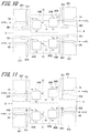
- FIG. 11 is a schematic diagram showing the configuration of an amplifier according to an eleventh embodiment of the present invention, and is a schematic circuit diagram showing a dual-band amplifier configured by two amplifier circuits;
- FIG. 12 is a schematic diagram showing the configuration of an amplifier according to a twelfth embodiment of the present invention, and is a schematic circuit diagram showing a dual-band amplifier configured by two amplifier circuits;
- FIG. 13 is a schematic diagram showing the configuration of an amplifier according to a thirteenth embodiment of the present invention, and is a schematic circuit diagram showing a dual-band amplifier configured by two amplifier circuits.
- FIG. 1A and FIG. 1B are diagrams showing the configuration of a multi-band amplifier according to a first embodiment of the present invention.
- the multi-band amplifier according to the present embodiment is a multi-band amplifier adapted to concurrently amplify signals in a plurality of frequency bands from a first frequency band to an N-th frequency band (N is a natural number not less than 2).
- the multi-band amplifier includes a signal input terminal 1 and a signal output terminal 2 .
- the multi-band amplifier has a plurality of amplifier circuits from a first amplifier circuit to an N-th amplifier circuit, which are: amplifier circuits 10 , 20 . . . 50 . . . 70 .
- N is a natural number not less than 2.
- Each amplifier circuit is a “transistor amplifier circuit” formed by a FET (Field Effect Transistor), and the “transistor amplifier circuit” will be simply referred to as an “amplifier circuit” hereinafter.
- a first amplifier circuit 10 is provided with, in an input signal dividing part thereof (which corresponds to the input side of the amplifier circuit 10 ), an input-side blocking circuit 12 adapted to block signals in frequency bands other than the first frequency band.
- the amplifier circuit 10 is further provided with, in an output signal combining part thereof (which corresponds to the output side of the amplifier circuit 10 ), an output-side blocking circuit 13 adapted to block signals in frequency bands other than the first frequency band.
- the second amplifier circuit 20 is provided with, in an input signal dividing part and an output signal combining part thereof, an input-side blocking circuit 22 and an output-side blocking circuit 23 respectively adapted to block signals in frequency bands other than the second frequency band.
- the N-th amplifier circuit 70 is provided with, in an input signal dividing part and an output signal combining part thereof, an input-side blocking circuit 72 and an output-side blocking circuit 73 respectively adapted to block signals in frequency bands other than the N-th frequency band.
- the signals in frequency bands other than the first frequency band are blocked by the input-side blocking circuit 12 , so that only the signal in the first frequency band is inputted into the amplifier circuit 10 .
- the signal in the first frequency band amplified by the amplifier circuit 10 is outputted from the signal output terminal 2 through the output-side blocking circuit 13 .
- the signals in the multi-bands applied to the multi-band amplifier from the signal input terminal 1 are blocked by the input-side blocking circuit 22 , so that only the signal in the second frequency band is inputted into the amplifier circuit 20 .
- the signal in the second frequency band amplified by the amplifier circuit 20 is outputted from the signal output terminal 2 through the output-side blocking circuit 23 .
- the signals in the multi-bands from the first frequency band to the N-th frequency band having been amplified by the amplifier circuits 10 , 20 . . . 50 . . . 70 are integrated and outputted from the signal output terminal 2 .
- each amplifier circuit of the present embodiment is formed by transistor(s)
- the amplification operation of the transistor(s) is not limited to a specific mode (such as Class-A, Class-B, Class-C, Class-F, Inverse Class-F, Class-E, harmonic reactance termination amplifier, Doherty amplifier or the like).
- each amplifier circuit may be configured as a multi-stage amplifier circuit, instead of being limited to a single-stage amplifier.
- the number of the stages of the amplifier circuit for each frequency does not have to be the same.
- the amplifier circuit for the signal in each of the plurality of frequency bands may be configured independently of the amplifier circuits for other frequency bands, and characteristics of the plurality of frequency bands may be set independently of each other.
- Each amplifier circuit includes a FET (which is an amplifying element), an input impedance matching circuit arranged on the input side of the FET, and an output impedance matching circuit arranged on the output side of the FET.
- the input impedance matching circuit and the output impedance matching circuit of the n-th amplifier circuit 50 include the input-side blocking circuit 52 and the output-side blocking circuit 53 (which both block the signals in frequency bands other than the n-th frequency band), and are adapted to perform input impedance matching and output impedance matching with respect to the transistor (which is an amplifying element).
- the input impedance matching circuit is designed such that the impedance when viewing the side of the signal source from the FET is equal to a signal source impedance Z ST1 of the FET which achieves the maximum power added efficiency of the FET.
- the output impedance matching circuit is designed such that the impedance when viewing the side of the load from the FET is equal to a load impedance Z LT1 of the FET which achieves the maximum power added efficiency of the FET.
- the input impedance matching circuit and the output impedance matching circuit perform a function for converting a signal source impedance Z S1 and a load impedance Z L1 when viewing the input-side blocking circuit 52 and the output-side blocking circuit 53 from the amplifier circuit 50 respectively into the signal source impedance Z ST1 and the load impedance Z LT1 of the FET (which both achieve the maximum power added efficiency of the FET).
- optimal characteristics can be achieved for each frequency band.
- FIG. 1B is a diagram showing an example in which the input impedance matching circuit is arranged on the input side of the FET, and the output impedance matching circuit is arranged on the output side of the FET.
- the first amplifier circuit 10 includes a FET 11 (which is an amplifying element), and has an input impedance matching circuit 14 arranged therein, wherein the input impedance matching circuit 14 is adapted to perform input impedance matching with respect to the signal in the first frequency band of the FET 11 and achieve reactance termination with respect to a second harmonic.
- the first amplifier circuit 10 has an output impedance matching circuit 15 arranged therein, wherein the output impedance matching circuit 15 is adapted to perform output impedance matching with respect to the signal in the first frequency band of the FET 11 and achieve reactance termination with respect to a second harmonic and a third harmonic.
- the input impedance matching circuit 14 performs reactance termination with respect to the second harmonic and the output impedance matching circuit 15 performs reactance termination with respect to the second harmonic and the third harmonic; the input impedance matching circuit 14 and the output impedance matching circuit 15 may also performs reactance termination with respect to further higher harmonic.
- the other amplifier circuits 20 , 50 , 70 include a FET 21 , a FET 51 and a FET 51 (each being an amplifying element) respectively, and have an input impedance matching circuit 24 , an input impedance matching circuit 54 and an input impedance matching circuit 74 (each having the same configuration as that of the input impedance matching circuit 14 ) arranged in the pre-stage of the FET 21 , the FET 51 and the FET 51 respectively.
- the other amplifier circuits 20 , 50 , 70 have an output impedance matching circuit 25 , an output impedance matching circuit 55 and an output impedance matching circuit 75 (each having the same configuration as that of the output impedance matching circuit 15 ) arranged in the rear-stage of the FET 21 , the FET 51 and the FET 51 respectively.
- the input impedance matching circuits 14 , 24 , 54 , 74 are each designed such that the impedance when viewing the side of the signal source from the FET 11 , 21 , 51 , 71 is equal to the signal source impedance Z ST1 of the FET 11 , 21 , 51 , 71 which achieve the maximum power added efficiency of the FET 11 , 21 , 51 , 71 .
- the output impedance matching circuits 15 , 25 , 55 , 75 are each designed such that the impedance when viewing the side of the load from the FET 11 , 21 , 51 , 71 is equal to the load impedance Z LT1 of the FET 11 , 21 , 51 , 71 which achieve the maximum power added efficiency of the FET 11 , 21 , 51 , 71 .
- the input impedance matching circuits 14 , 24 , 54 , 74 and the output impedance matching circuits 15 , 25 , 55 , 75 are each formed by a distributed constant circuit such as a microstrip line, for example.
- FIG. 2 is a schematic diagram showing the configuration of an amplifier according to a second embodiment of the present invention, and is a schematic circuit diagram showing a dual-band amplifier configured by two transistor amplifier circuits (which will each be simply referred to as an “amplifier circuit” hereinafter).
- the dual-band amplifier includes a signal input terminal 3 and a signal output terminal 4 .
- the dual-band amplifier has two amplifier circuits 30 , 40 .
- the first amplifier circuit 30 is provided with, in an input signal dividing part thereof (which corresponds to the input side of the first amplifier circuit 30 ), an input-side blocking circuit 32 adapted to block the signal in a second frequency band.
- the first amplifier circuit 30 is provided with, in an output signal combining part thereof (which corresponds to the output side of the first amplifier circuit 30 ), an output-side blocking circuit 33 adapted to block the signal in the second frequency band.
- the second amplifier circuit 40 is provided with, in an input signal dividing part and an output signal combining part thereof, an input-side blocking circuit 42 and an output-side blocking circuit 43 adapted to block the signal in the first frequency band.
- the signal in the first frequency band is inputted into the first amplifier circuit 30 through the input-side blocking circuit 32 which blocks the signal in the second frequency band.
- the signal in the first frequency band amplified by the first amplifier circuit 30 is outputted from the signal output terminal 4 through the output-side blocking circuit 33 which blocks the signal in the second frequency band.
- the impedance when viewing the input-side blocking circuit 32 (which blocks the signal in the second frequency band) from the signal input terminal 3 is open for the second frequency band.
- the impedance when viewing the output-side blocking circuit 33 (which blocks the signal in the second frequency band) from the signal output terminal 4 is also open for the second frequency band.
- the signal in the second frequency band is inputted into the second amplifier circuit 40 through the input-side blocking circuit 42 (which blocks the signal in the first frequency band) and is amplified by the second amplifier circuit 40 . Further, the signal in the second frequency band is outputted from the signal output terminal 4 of the dual-band amplifier through the output-side blocking circuit 43 which blocks the signal in the first frequency band.
- the impedance when viewing the input-side blocking circuit 42 and the output-side blocking circuit 43 (which both block the signal in the first frequency band) respectively from the signal input terminal 3 and the signal output terminal 4 is open for the first frequency band.
- the first amplifier circuit 30 includes a FET 31 (which is an amplifying element), an input impedance matching circuit arranged on the input side of the FET 31 , and an output impedance matching circuit 35 arranged on the output side of the FET 31 .
- the input impedance matching circuit 34 and the output impedance matching circuit 35 include the input-side blocking circuit 32 and the output-side blocking circuit 33 (which both block the signal in the second frequency band), and are adapted to perform input/output impedance matching with respect to the transistor FET 31 (which is an amplifying element).
- the input impedance matching circuit 34 is designed such that the impedance when viewing the side of the signal source from the FET 31 is equal to a signal source impedance Z ST1 of the FET 31 which achieves the maximum power added efficiency of the FET 31 .
- the output impedance matching circuit 35 is designed such that the impedance when viewing the side of the load from the FET 31 is equal to a load impedance Z LT1 of the FET 31 which achieves the maximum power added efficiency of the FET 31 .
- the input impedance matching circuit 34 and the output impedance matching circuit 35 perform a function for converting a signal source impedance Z S1 and a load impedance Z L1 when viewing the input-side blocking circuit 32 and the output-side blocking circuit 33 from the first amplifier circuit 30 respectively into the signal source impedance Z ST1 and the load impedance Z LT1 of the FET 31 (which both achieve the maximum power added efficiency of the FET 31 ).
- the second amplifier circuit 40 includes a FET 41 (which is an amplifying element), an input impedance matching circuit arranged on the input side of the FET 41 , and an output impedance matching circuit 45 arranged on the output side of the FET 41 .
- the input impedance matching circuit 44 and the output impedance matching circuit 45 convert a signal source impedance Z S2 and a load impedance Z L2 when viewing the input-side blocking circuit 42 and the output-side blocking circuit (which both block the signal in the first frequency band) from the amplifier circuit 40 respectively into the signal source impedance Z ST2 and the load impedance Z LT2 of the FET 41 (which both achieve the maximum power added efficiency of the FET 41 ).
- the frequency blocking circuits and the impedance matching circuits of the amplifier circuits By designing the frequency blocking circuits and the impedance matching circuits of the amplifier circuits in the aforesaid manner, it is possible to obtain a concurrent dual-band power amplifier adapted to achieve maximum power added efficiency characteristics for the signal in each frequency band. Further, as described above, since the matching circuits of the amplifier circuit to amplify the signal in each frequency band can be independently designed, it is possible to freely select the type of the FET and the gate width; and also, since accuracy of optimal design relevant to power efficiency and output power becomes higher, it becomes easy to achieve high efficiency power characteristics. Further, in the amplifier of the present invention, since the signal in each frequency band is amplified by an independent amplifier circuit, no distortion such as intermodulation, cross modulation and the like will be caused between signals in different frequency bands.
- the present embodiment is described based on a case where the transistor amplifier circuit is a single-stage amplifier, obviously the present invention also include a case where the transistor amplifier circuit is a multi-stage amplifier circuit.
- the amplification operation of the transistor(s) is not limited to a specific mode (such as Class-A, Class-B, Class-C, Class-F, Inverse Class-F, Class-E, harmonic reactance termination amplifier, Doherty amplifier or the like)
- an output power (dBm) P out with respect to an input power (dBm), a power added efficiency (PAE) % with respect to the input power (dBm), and a drain efficiency ⁇ (%) will be described below with reference to FIG. 3 .
- the first amplifier circuit 30 amplifies the signal in the first frequency band (f 1 ), and the second amplifier circuit amplifies the signal in the second frequency band (f 2 ).
- the frequency of the signal in the first frequency band (f 1 ) is 4.5 GHz
- the frequency of the signal in the second frequency band (f 2 ) is 8.5 GHz.
- FIG. 3A shows an output power P out (f 1 ) of a signal in the first frequency band (f 1 ) and an output power P out (f 2 ) of a signal in the second frequency band (f 2 ), a power added efficiency PAE (f 1 ) of the signal in the first frequency band (f 1 ) and a power added efficiency PAE (f 2 ) of the signal in the second frequency band (f 2 ), and a drain efficiency ⁇ D (f 1 ) of the signal in the first frequency band (f 1 ) and a drain efficiency ⁇ D (f 2 ) of the signal in the second frequency band (f 2 ).
- the solid line represents characteristics of the signal in the first frequency band (f 1 )
- the broken line represents characteristics of the signal in the second frequency band (f 2 ).
- the power added efficiencies PAE (f 1 ) and PAE (f 2 ) are obtained from [(output power P out ⁇ input power P in )/amplifier power P DC ]“.
- the amplifier power P DC represents DC power supplied to the amplifying element.
- the drain efficiencies ⁇ D (f 1 ) and ⁇ D (f 2 ) are obtained from [output power P out /amplifier power P DC ]”.
- the output power P out with respect to the input power P in have sufficient level for the signals in the first and second frequency bands (f 2 , f 2 ), and are excellent characteristics with respect to the power added efficiencies PAE and the drain efficiencies ⁇ D .
- FIG. 3B shows each frequency component included the output power (dBm).
- the output power (dBm) spectrum is obtained in a condition where the input power P in of the signal in the first frequency band (f 1 ) is 29 dBm and the input power P in of the signal in the second frequency band (f 2 ) is 32 dBm.
- harmonics 2f 1 , 3f 1 , . . . of the first frequency f 1 are sufficiently suppressed, and harmonics 2f 2 , of the second frequency f 2 are also sufficiently suppressed.
- frequency components of the difference between the first frequency f 1 and the second frequency f 2 such as [f 2 ⁇ f 1 ] are sufficiently small compared with the frequencies f 1 , and also, intermodulation distortion is sufficiently suppressed.
- FIG. 4 is a schematic diagram showing the configuration of an amplifier according to a third embodiment of the present invention, and is a schematic circuit diagram showing a dual-band amplifier configured by two transistor amplifier circuits (which will each be simply referred to as an “amplifier circuit” hereinafter). Note that, the same components shown in FIG. 4 are denoted by the same numerals as of FIG. 2 and the explanation thereof will not be repeated.
- a first amplifier circuit 30 is provided with, in an input signal dividing part thereof (which corresponds to the input side of the first amplifier circuit 30 ), an input-side blocking circuit 36 adapted to block the signal in a second frequency band.
- the input-side blocking circuit 36 is a circuit whose parallel resonance frequency falls in the second frequency band, and is connected in series with the amplifier circuit 30 . Since the impedance of a parallel resonance circuit is close to open at the parallel resonance frequency, by connecting the input-side blocking circuit 36 in series with the amplifier circuit 30 , the signal in the second frequency band can be blocked from being inputted into the first amplifier circuit 30 .
- the first amplifier circuit 30 is provided with, in an output signal combining part thereof (which corresponds to the output side of the first amplifier circuit 30 ), an output-side blocking circuit 37 adapted to block the signal in the second frequency band. Similar to the input-side blocking circuit 36 , the output-side blocking circuit 37 is also a circuit whose parallel resonance frequency falls in the second frequency band, and is connected in series with the amplifier circuit 30 .
- the second amplifier circuit 40 is provided with, in an input signal dividing part and an output signal combining part thereof, an input-side blocking circuit 46 and an output-side blocking circuit 47 adapted to block the signal in the first frequency band.
- the signal in the first frequency band is inputted into the first amplifier circuit 30 through the input-side blocking circuit 36 .
- the signal in the first frequency band amplified by the first amplifier circuit 30 is outputted from the signal output terminal 4 through the output-side blocking circuit 37 .
- the impedance when viewing the input-side blocking circuit 36 (which blocks the signal in the second frequency band) from the signal input terminal 3 is open for the second frequency band. Further, the impedance when viewing the output-side blocking circuit 37 (which blocks the signal in the second frequency band) from the signal output terminal 4 is also open.
- the signal in the second frequency band is inputted into the second amplifier circuit 40 through the input-side blocking circuit 46 (which blocks the signal in the first frequency band) and amplified by the second amplifier circuit 40 . Further, the signal in the second frequency band is outputted from the signal output terminal 4 of the dual-band amplifier through the output-side blocking circuit 47 which blocks the signal in the first frequency band.
- the impedance when viewing the input-side blocking circuit 46 and the output-side blocking circuit 47 (which both block the signal in the first frequency band) respectively from the signal input terminal 3 and the signal output terminal 4 is open for the first frequency band.
- the first amplifier circuit 30 includes a FET 31 (which is an amplifying element), an input impedance matching circuit arranged on the input side of the FET 31 , and an output impedance matching circuit 35 arranged on the output side of the FET 31 .
- the input impedance matching circuit 34 and the output impedance matching circuit 35 include the input-side blocking circuit 36 and the output-side blocking circuit 37 (which both block the signal in the second frequency band), and are adapted to perform input/output impedance matching with respect to the transistor FET 31 (which is an amplifying element).
- the input impedance matching circuit 34 is designed such that the impedance when viewing the side of the signal source from the FET 31 is equal to a signal source impedance Z ST1 of the FET 31 which achieves the maximum power added efficiency of the FET 31 .
- the output impedance matching circuit 35 is designed such that the impedance when viewing the side of the load from the FET 31 is equal to a load impedance Z LT1 of the FET 31 which achieves the maximum power added efficiency of the FET 31 .
- the input impedance matching circuit 34 and the output impedance matching circuit 35 perform a function for converting a signal source impedance Z S1 and a load impedance Z L1 when viewing the input-side blocking circuit 36 and the output-side blocking circuit 37 from the first amplifier circuit 30 respectively into the signal source impedance Z ST1 and the load impedance Z LT1 of the FET 31 (which both achieve the maximum power added efficiency of the FET 31 ).
- the second amplifier circuit 40 includes a FET 41 (which is an amplifying element), an input impedance matching circuit arranged on the input side of the FET 41 , and an output impedance matching circuit 45 arranged on the output side of the FET 41 .
- the input impedance matching circuit 44 and the output impedance matching circuit 45 convert a signal source impedance Z S2 and a load impedance Z L2 when viewing the input-side blocking circuit 46 and the output-side blocking circuit (which both block the signal in the first frequency band) from the amplifier circuit 40 respectively into the signal source impedance Z ST2 and the load impedance Z LT2 of the FET 41 (which both achieve the maximum power added efficiency of the FET 41 ).
- FIG. 5 is a schematic diagram showing the configuration of an amplifier according to a fourth embodiment of the present invention, and is a schematic circuit diagram showing a dual-band amplifier configured by two transistor amplifier circuits (which will each be simply referred to as an “amplifier circuit” hereinafter). Note that, the same components shown in FIG. 5 are denoted by the same numerals as of FIG. 2 and the explanation thereof will not be repeated.
- a circuit denoted by a reference numeral ending with A, B, C or D may have different configuration from the original circuit (such as the amplifier circuit 30 , the amplifier circuit 40 or the like).
- the dual-band amplifier has two amplifier circuits 30 A, 40 A.
- the first amplifier circuit 30 A is provided with, in an input signal dividing part thereof (which corresponds to the input side of the first amplifier circuit 30 A), an input-side blocking circuit 57 adapted to block the signal in a second frequency band.
- the input-side blocking circuit 57 includes an input-side blocking circuit 36 and a circuit element 56 , wherein the input-side blocking circuit 36 is a circuit whose parallel resonance frequency falls in the second frequency band, and the circuit element 56 is adapted to cancel a series reactance component of the input-side blocking circuit 36 in a first frequency band.
- the input-side blocking circuit 36 and the circuit element 56 are connected to each other in series to form the input-side blocking circuit 57 .
- the first amplifier circuit 30 A is provided with, in an output signal combining part thereof (which corresponds to the output side of the first amplifier circuit 30 A), an output-side blocking circuit 59 adapted to block the signal in the second frequency band.
- the output-side blocking circuit 59 includes an output-side blocking circuit 37 and a circuit element 58 , wherein the output-side blocking circuit is a circuit whose parallel resonance frequency falls in the second frequency band, and the circuit element 58 is adapted to cancel a series reactance component of the output-side blocking circuit 37 in the first frequency band.
- the output-side blocking circuit 37 and the circuit element 58 are connected to each other in series to form the output-side blocking circuit 59 .
- the second amplifier circuit 40 A is provided with, in an input signal dividing part thereof (which corresponds to the input side of the second amplifier circuit 40 A), an input-side blocking circuit 67 adapted to block the signal in the first frequency band.
- the input-side blocking circuit 67 includes an input-side blocking circuit 46 and a circuit element 66 , wherein input-side blocking circuit 46 is a circuit whose parallel resonance frequency falls in the first frequency band, and the circuit element 66 is adapted to cancel a series reactance component of the input-side blocking circuit 46 in the second frequency band.
- the input-side blocking circuit 46 and the circuit element 66 are connected to each other in series to form the input-side blocking circuit 67 .
- the second amplifier circuit 40 A is provided with, in an output signal combining part thereof (which corresponds to the output side of the second amplifier circuit 60 ), an output-side blocking circuit 69 adapted to block the signal in the first frequency band.
- the output-side blocking circuit 69 includes an output-side blocking circuit 47 and a circuit element 68 , wherein output-side blocking circuit 47 is a circuit whose parallel resonance frequency falls in the first frequency band, and the circuit element 68 is adapted to cancel a series reactance component of the output-side blocking circuit 47 in the second frequency band.
- the output-side blocking circuit 47 and the circuit element 68 are connected to each other in series to form the output-side blocking circuit 69 .
- the signal in the first frequency band is inputted into the first amplifier circuit 30 A through the input-side blocking circuit 57 .
- the signal in the first frequency band amplified by the first amplifier circuit 30 A is outputted from the signal output terminal 4 through the output-side blocking circuit 59 .
- the impedance when viewing the input-side blocking circuit 57 (which blocks the signal in the second frequency band) from the signal input terminal 3 is open for second frequency band.
- the impedance when viewing the output-side blocking circuit 59 (which blocks the signal in the second frequency band) from the signal output terminal 4 is also open for second frequency band.
- the signal in the second frequency band is inputted into the second amplifier circuit 40 A through the input-side blocking circuit 67 (which blocks the signal in the first frequency band) and amplified by the second amplifier circuit 40 A.
- the signal in the second frequency band is outputted from the signal output terminal 4 of the dual-band amplifier through the output-side blocking circuit 69 (which blocks the signal in the first frequency band).
- the impedance when viewing the input-side blocking circuit 67 and the output-side blocking circuit 69 (which both block the signal in the first frequency band) respectively from the signal input terminal 3 and the signal output terminal 4 is open for the first frequency band.
- the first amplifier circuit 30 A includes a FET 51 (which is an amplifying element), an input impedance matching circuit arranged on the input side of the FET 51 , and an output impedance matching circuit 55 arranged on the output side of the FET 51 .
- the input impedance matching circuit 54 and the output impedance matching circuit 55 include the input-side blocking circuit 57 and the output-side blocking circuit 59 (which both block the signal in the second frequency band), and are adapted to perform input/output impedance matching with respect to the transistor FET 51 (which is an amplifying element).
- the input impedance matching circuit 54 is designed such that the impedance when viewing the side of the signal source from the FET 51 is equal to a signal source impedance Z ST1 of the FET 51 which achieves the maximum power added efficiency of the FET 51 .
- the output impedance matching circuit 55 is designed such that the impedance when viewing the side of the load from the FET 51 is equal to a load impedance Z LT1 of the FET 51 which achieves the maximum power added efficiency of the FET 51 .
- the input impedance matching circuit 54 and the output impedance matching circuit 55 perform a function for converting a signal source impedance Z S1 and a load impedance Z L1 when viewing the input-side blocking circuit 57 and the output-side blocking circuit 59 from the first amplifier circuit 30 A respectively into the signal source impedance Z ST1 and the load impedance Z LT1 of the FET 51 (which both achieve the maximum power added efficiency of the FET 51 ).
- reactance components of the input-side blocking circuit 57 and the output-side blocking circuit 59 (which both block the signal in the second frequency band) are cancelled, the signal source impedance Z S1 and the load impedance Z L1 viewed from the first amplifier circuit 30 A are each 50 ⁇ .
- the second amplifier circuit 40 A includes a FET 61 (which is an amplifying element), an input impedance matching circuit arranged on the input side of the FET 61 , and an output impedance matching circuit 65 arranged on the output side of the FET 41 .
- the input impedance matching circuit 64 and the output impedance matching circuit 65 convert a signal source impedance Z S2 and a load impedance Z L2 when viewing the input-side blocking circuit 67 and the output-side blocking circuit (which both block the signal in the first frequency band) from the second amplifier circuit 40 A respectively into the signal source impedance Z ST2 and the load impedance Z LT2 of the FET 41 (which both achieve the maximum power added efficiency of the FET 41 ).
- the signal source impedance Z S2 and the load impedance Z L2 viewed from the second amplifier circuit 40 A are each 50 ⁇ .
- the signal source impedance and the load impedance of each of the two amplifier circuits constituting the dual-band amplifier are each 50 ⁇ , which is the standard impedance, and therefore it becomes easy to design and evaluate the impedance matching circuits, so that it is advantageous to enhance performance.
- the input-side blocking circuit 36 and the output-side blocking circuit 37 of the third and fourth embodiments whose parallel resonance frequency falls into the second frequency band are each formed by an inductor and a capacitor connected in parallel.
- the input-side blocking circuit 46 and the output-side blocking circuit 47 of the third and fourth embodiments whose parallel resonance frequency falls into the second frequency band are each formed by an inductor and a capacitor connected in parallel.
- FIG. 6 is a schematic diagram showing the configuration of an amplifier according to a sixth embodiment of the present invention, and is a schematic circuit diagram showing a dual-band amplifier configured by two transistor amplifier circuits (which will each be simply referred to as an “amplifier circuit” hereinafter). Note that, the same components shown in FIG. 6 are denoted by the same numerals as of FIG. 2 and the explanation thereof will not be repeated.
- a first amplifier circuit 30 is provided with, in an input signal dividing part thereof (which corresponds to the input side of the first amplifier circuit 30 ), an input-side blocking circuit 32 adapted to block the signal in a second frequency band.
- the input-side blocking circuit 32 has a series transmission line 72 and a parallel circuit 73 , wherein the series transmission line 72 is a component whose characteristic impedance is 50 ⁇ and whose length is equal to a quarter of the wavelength of the signal in the second frequency band, and the parallel circuit 73 is adapted to short-circuit the signal in the second frequency band.
- the transmission line 72 is connected in series with the main line, and the parallel circuit 73 is connected in parallel to the main line to form the input-side blocking circuit 32 .
- the first amplifier circuit 30 is provided with, in an output signal combining part thereof (which corresponds to the output side of the first amplifier circuit 30 ), an output-side blocking circuit 33 adapted to block the signal in the second frequency band.
- the output-side blocking circuit 32 has a series transmission line 74 and a parallel circuit 75 , wherein the series transmission line 74 is a component whose characteristic impedance is 50 ⁇ and whose length is equal to a quarter of the wavelength of the signal in the second frequency band, and the parallel circuit 75 is adapted to short-circuit the signal in the second frequency band.
- the transmission line 74 is connected in series with the main line, and the parallel circuit 75 is connected in parallel to the main line to form the output-side blocking circuit 33 .
- the second amplifier circuit 40 is provided with, in an input signal dividing part thereof (which corresponds to the input side of the second amplifier circuit 40 ), an input-side blocking circuit 42 adapted to block the signal in a first frequency band.
- the input-side blocking circuit 42 has a series transmission line 82 and a parallel circuit 83 , wherein the series transmission line 82 is a component whose characteristic impedance is 50 ⁇ and whose length is equal to a quarter of the wavelength of the signal in the first frequency band, and the parallel circuit 73 is adapted to short-circuit the signal in the first frequency band.
- the transmission line 82 is connected in series with the main line, and the parallel circuit 83 is connected in parallel to the main line to form the input-side blocking circuit 42 .
- the second amplifier circuit 40 is provided with, in an output signal combining part thereof (which corresponds to the output side of the second amplifier circuit 40 ), an output-side blocking circuit 43 adapted to block the signal in the first frequency band.
- the output-side blocking circuit 43 has a series transmission line 84 and a parallel circuit 85 , wherein the series transmission line 84 is a component whose characteristic impedance is 50 ⁇ and whose length is equal to a quarter of the wavelength of the signal in the first frequency band, and the parallel circuit 85 is adapted to short-circuit the signal in the first frequency band.
- the transmission line 84 is connected in series with the main line, and the parallel circuit 85 is connected in parallel to the main line to form the output-side blocking circuit 43 .
- the signal in the first frequency band is inputted into the first amplifier circuit 30 through the input-side blocking circuit 32 .
- the signal in the first frequency band amplified by the first amplifier circuit 30 is outputted from the signal output terminal 4 through the output-side blocking circuit 33 .
- the impedance when viewing the input-side blocking circuit 32 (which blocks the signal in the second frequency band) from the signal input terminal 4 is open for the second frequency band.
- the impedance when viewing the output-side blocking circuit 33 (which blocks the signal in the second frequency band) from the signal output terminal 4 is also open for the second frequency band.
- the signal in the second frequency band is inputted into the second amplifier circuit 40 through the input-side blocking circuit 42 (which blocks the signal in the first frequency band) and is amplified by the second amplifier circuit 40 . Further, the signal in the second frequency band is outputted from the signal output terminal 4 of the dual-band amplifier through the output-side blocking circuit 43 which blocks the signal in the first frequency band.
- the impedance when viewing the input-side blocking circuit 42 and the output-side blocking circuit 43 (which both block the signal in the first frequency band) respectively from the signal input terminal 3 and the signal output terminal 4 is open for the first frequency band.
- the first amplifier circuit 30 includes a FET 31 (which is an amplifying element), an input impedance matching circuit arranged on the input side of the FET 31 , and an output impedance matching circuit 35 arranged on the output side of the FET 31 .
- the input impedance matching circuit 34 and the output impedance matching circuit 35 include the input-side blocking circuit 32 and the output-side blocking circuit 33 (which both block the signal in the second frequency band), and are adapted to perform input/output impedance matching with respect to the transistor FET 31 (which is an amplifying element).
- the input impedance matching circuit 34 is designed such that the admittance when viewing the side of the signal source from the FET 31 is equal to a signal source admittance Y ST1 of the FET 31 which achieves the maximum power added efficiency of the FET 31 .
- the output impedance matching circuit 35 is designed such that the admittance when viewing the side of the load from the FET 31 is equal to a load admittance Y LT1 of the FET 31 which achieves the maximum power added efficiency of the FET 31 .
- the input impedance matching circuit 34 and the output impedance matching circuit 35 perform a function for converting a signal source admittance Y S1 and a load admittance Y L1 when viewing the input-side blocking circuit 32 and the output-side blocking circuit 33 from the first amplifier circuit 30 respectively into the signal source admittance Y ST1 and the load admittance Y LT1 of the FET 31 (which both achieve the maximum power added efficiency of the FET 31 ).
- the second amplifier circuit 40 includes a FET 41 (which is an amplifying element), an input impedance matching circuit arranged on the input side of the FET 41 , and an output impedance matching circuit 45 arranged on the output side of the FET 41 .
- the input impedance matching circuit 44 and the output impedance matching circuit 45 convert a signal source admittance Y S2 and a load admittance Y L2 when viewing the input-side blocking circuit 42 and the output-side blocking circuit (which both block the signal in the first frequency band) from the second amplifier circuit 40 respectively into the signal source admittance Y ST2 and the load admittance Y LT2 of the FET 41 (which both achieve the maximum power added efficiency of the FET 41 ).
- each of the parallel circuits 73 , 75 , 83 , adapted to short-circuit signals is not limited to a specific circuit/element, such as a transmission line with opened tip, a radial line, and a series resonance circuit formed by an inductor and a capacitive element.
- FIG. 7 is a schematic diagram showing the configuration of an amplifier according to a seventh embodiment of the present invention, and is a schematic circuit diagram showing a dual-band amplifier configured by two transistor amplifier circuits (which will each be simply referred to as an “amplifier circuit” hereinafter). Note that, the same components shown in FIG. 7 are denoted by the same numerals as of FIG. 2 and the explanation thereof will not be repeated.
- a first amplifier circuit 30 B is provided with, in an input signal dividing part thereof (which corresponds to the input side of the first amplifier circuit 30 B) an input-side blocking circuit 321 adapted to block the signal in a second frequency band.
- the input-side blocking circuit 321 has a series transmission line 72 , a parallel circuit 73 , and a circuit 38 , wherein the series transmission line 72 is a component whose characteristic impedance is 50 ⁇ and whose length is equal to a quarter of the wavelength of the signal in the second frequency band, the parallel circuit 73 is adapted to short-circuit the signal in the second frequency band, and the circuit 38 is adapted to cancel a susceptance component of the parallel circuit 73 in the first frequency band (the circuit 38 will be referred to as “cancellation circuit 38 ” hereinafter).
- the transmission line 72 is connected in series with the main line, and the parallel circuit 73 and the cancellation circuit 38 are connected in parallel to the main line to form the input-side blocking circuit 321 .
- the first amplifier circuit 30 B is provided with, in an output signal combining part thereof (which corresponds to the output side of the first amplifier circuit 30 B), an output-side blocking circuit 331 adapted to block the signal in the second frequency band.
- the output-side blocking circuit 331 has a series transmission line 74 , a parallel circuit 75 , and a circuit 39 , wherein the series transmission line 74 is a component whose characteristic impedance is 50 ⁇ and whose length is equal to a quarter of the wavelength of the signal in the second frequency band, the parallel circuit is adapted to short-circuit the signal in the second frequency band, and the circuit 39 is adapted to cancel a susceptance component of the parallel circuit 75 in the first frequency band (the circuit 39 will be referred to as “cancellation circuit 39 ” hereinafter).
- the transmission line 74 is connected in series with the main line, and the parallel circuit 75 and the cancellation circuit 39 are connected in parallel to the main line to form the output-side blocking circuit 331 .
- the second amplifier circuit 40 B is provided with, in an input signal dividing part thereof, an input-side blocking circuit 421 adapted to block the signal in a first frequency band.
- the input-side blocking circuit 421 has a series transmission line 82 , a parallel circuit 83 , and a circuit 48 , wherein the series transmission line 82 is a component whose characteristic impedance is 50 ⁇ and whose length is equal to a quarter of the wavelength of the signal in the first frequency band, the parallel circuit 83 is adapted to short-circuit the signal in the first frequency band, and the circuit 48 is adapted to cancel a susceptance component of the parallel circuit 83 in the second frequency band (the circuit 48 will be referred to as “cancellation circuit 48 ” hereinafter).
- the second amplifier circuit 40 B is provided with, in an output signal combining part thereof, an output-side blocking circuit 431 adapted to block the signal in the first frequency band.
- the output-side blocking circuit 431 has a series transmission line 84 , a parallel circuit 85 , and a circuit 49 , wherein the series transmission line 82 is a component whose characteristic impedance is 50 ⁇ and whose length is equal to a quarter of the wavelength of the signal in the first frequency band, the parallel circuit 85 is adapted to short-circuit the signal in the first frequency band, and the circuit 49 is adapted to cancel a susceptance component of the parallel circuit 85 in the second frequency band (the circuit 49 will be referred to as “cancellation circuit 49 ” hereinafter).
- the signal in the first frequency band is inputted into the first amplifier circuit 30 B through the input-side blocking circuit 321 .
- the signal in the first frequency band amplified by the first amplifier circuit 30 B is outputted from the signal output terminal 4 through the output-side blocking circuit 331 .
- the impedance when viewing the input-side blocking circuit 321 (which blocks the signal in the second frequency band) from the signal input terminal 3 is open for the second frequency band.
- the impedance when viewing the output-side blocking circuit 331 (which blocks the signal in the second frequency band) from the signal output terminal 4 is also open for the second frequency band.
- the signal in the second frequency band is inputted into the second amplifier circuit 40 B through the input-side blocking circuit 421 (which blocks the signal in the first frequency band) and amplified by the second amplifier circuit 40 B.
- the signal in the second frequency band is outputted from the signal output terminal 4 of the dual-band amplifier through the output-side blocking circuit 431 (which blocks the signal in the first frequency band).
- the impedance when viewing the input-side blocking circuit 421 and the output-side blocking circuit 431 (which both block the signal in the first frequency band) respectively from the signal input terminal 3 and the signal output terminal 4 is open for the first frequency band.
- the first amplifier circuit 30 B includes a FET 31 (which is an amplifying element), an input impedance matching circuit 34 B arranged on the input side of the FET 31 , and an output impedance matching circuit 35 B arranged on the output side of the FET 31 .
- the input impedance matching circuit 34 B and the output impedance matching circuit 35 B include the input-side blocking circuit 321 and the output-side blocking circuit 331 (which both block the signal in the second frequency band), and are adapted to perform input/output impedance matching with respect to the transistor FET 31 (which is an amplifying element).
- the input impedance matching circuit 34 B is designed such that the admittance when viewing the side of the signal source from the FET 31 is equal to a signal source admittance Y ST1 of the FET 31 which achieves the maximum power added efficiency of the FET 31 .
- the output impedance matching circuit 35 B is designed such that the admittance when viewing the side of the load from the FET 31 is equal to a load admittance Y LT1 of the FET 31 which achieves the maximum power added efficiency of the FET 31 .
- the second amplifier circuit 40 B includes a FET 41 (which is an amplifying element), an input impedance matching circuit 44 B arranged on the input side of the FET 41 , and an output impedance matching circuit 45 B arranged on the output side of the FET 41 .
- the signal source impedance and the load impedance viewed from each amplifier circuit are each 50 ⁇ , it becomes easy to design and evaluate each amplifier circuit.
- each of the parallel circuits 73 , 75 , 83 adapted to short-circuit signals is not limited to a specific circuit/element, such as a transmission line with opened tip, a radial line, and a serial resonance circuit formed by an inductor and a capacitive element.
- Each of the cancellation circuits 38 , 39 , 48 , 49 adapted to cancel susceptance components is not limited to a specific circuit/element, such as a transmission line, a radial line, an inductor and a capacitive element.
- FIG. 8 is a schematic diagram showing the configuration of an amplifier according to an eighth embodiment of the present invention, and is a schematic circuit diagram showing a dual-band amplifier configured by two transistor amplifier circuits (which will each be simply referred to as an “amplifier circuit” hereinafter). Note that, the same components shown in FIG. 8 are denoted by the same numerals as of FIG. 6 and the explanation thereof will not be repeated.
- the eighth embodiment is characterized in that the circuits 73 , 75 , 83 , 85 adapted to short signals in respective frequency bands in input-side blocking circuits 32 C, 42 C and output-side blocking circuits 33 C, 43 C (which block signals in respective frequency bands) are formed by parallel stubs 731 , 751 , 831 , 851 whose tips are opened.
- the input-side blocking circuit 32 C and the output-side blocking circuit 33 C (which both block the signal in the second frequency band) are formed by series transmission lines 72 , and 74 and the parallel stubs 731 and 751 adapted to short the signal in the second frequency band, wherein the series transmission lines 72 and 74 are each a component whose characteristic impedance is 50 ⁇ and whose length is equal to a quarter of the wavelength of the signal in the second frequency band, and wherein the parallel stubs 731 and 751 are each a component whose tip is opened which has a strip line configuration whose length is equal to a quarter of the wavelength of the signal in the second frequency band.
- an input-side blocking circuit 42 C and an output-side blocking circuit 43 C (which both block the signal in the first frequency band) are formed by series transmission lines 82 , and 84 and the parallel stubs 831 and 851 adapted to short-circuit the signal in the first frequency band, wherein the series transmission lines 82 and 84 are each a component whose characteristic impedance is 50 ⁇ and whose length is equal to a quarter of the wavelength of the signal in the first frequency band, and wherein the parallel stubs 831 and 851 are each a component whose tip is opened and which has a strip line configuration whose length is equal to a quarter of the wavelength of the signal in the first frequency band.
- the first amplifier circuit 30 C connected to the input-side blocking circuit 32 C includes a FET 31 (which is an amplifying element), an input impedance matching circuit 34 C arranged on the input side of the FET 31 , and an output impedance matching circuit 35 C arranged on the output side of the FET 31 .
- the output impedance matching circuit 35 C is connected to the output-side blocking circuit 33 C.
- a second amplifier circuit 40 C connected to the input-side blocking circuit 42 C includes a FET 41 (which is an amplifying element), an input impedance matching circuit 44 C arranged on the input side of the FET 41 , and an output impedance matching circuit 45 C arranged on the output side of the FET 41 .
- the output impedance matching circuit 45 C is connected to the output-side blocking circuit 43 C.
- the parallel stub is not limited to a specific transmission line such as a coplanar transmission line, a radial line and the like.
- FIG. 9 is a schematic diagram showing the configuration of an amplifier according to a ninth embodiment of the present invention, and is a schematic circuit diagram showing a dual-band amplifier configured by two transistor amplifier circuits (which will each be simply referred to as an “amplifier circuit” hereinafter). Note that, the same components shown in FIG. 9 are denoted by the same numerals as of FIG. 6 and the explanation thereof will not be repeated.
- the ninth embodiment is characterized in that the circuits 73 , 75 , 83 , 85 adapted to short-circuit signals in respective frequency bands in input-side blocking circuits 32 D, 42 D and output-side blocking circuits 33 D, 43 D (which block signals in respective frequency bands) are formed by inductor-capacitor series circuits 732 , 752 , 832 , 852 .
- the input-side blocking circuit 32 D and the output-side blocking circuit 33 D (which both block the signal in the second frequency band) are formed by series transmission lines 72 and 74 and the inductor-capacitor series circuits 732 and 752 , wherein the series transmission lines 72 and 74 are each a component whose characteristic impedance is 50 ⁇ and whose length is equal to a quarter of the wavelength of the signal in the second frequency band, and wherein the inductor-capacitor series circuits 732 and 752 become series resonance short-circuited with respect to the signal in the second frequency band.
- An input-side blocking circuit 42 D and an output-side blocking circuit 43 D (which both block the signal in the first frequency band) are formed by series transmission lines 82 and and the inductor-capacitor series circuits 832 and 852 , wherein the series transmission lines 82 and 84 are each a component whose characteristic impedance is 50 ⁇ and whose length is equal to a quarter of the wavelength of the signal in the first frequency band, and wherein the inductor-capacitor series circuits 832 and 852 become series resonance short-circuited with respect to the signal in the first frequency band.
- a first amplifier circuit 30 D connected to the input-side blocking circuit 32 D includes a FET 31 (which is an amplifying element), an input impedance matching circuit 34 D arranged on the input side of the FET 31 , and an output impedance matching circuit 35 D arranged on the output side of the FET 31 .
- the output impedance matching circuit 35 D is connected to the output-side blocking circuit 33 D.
- a second amplifier circuit 40 D connected to the input-side blocking circuit 42 D includes a FET 41 (which is an amplifying element), an input impedance matching circuit 44 D arranged on the input side of the FET 41 , and an output impedance matching circuit 45 D arranged on the output side of the FET 41 .
- the output impedance matching circuit 45 D is connected to the output-side blocking circuit 43 D.
- FIG. 10 is a schematic diagram showing the configuration of an amplifier according to a tenth embodiment of the present invention, and is a schematic circuit diagram showing a dual-band amplifier configured by two transistor amplifier circuits (which will each be simply referred to as an “amplifier circuit” hereinafter). Note that, the same components shown in FIG. 10 are denoted by the same numerals as of FIG. 7 and the explanation thereof will not be repeated.
- the tenth embodiment is characterized in that the circuits 73 , 75 , 83 , 85 adapted to short-circuit signals in respective frequency bands in the input-side blocking circuits 321 , 421 and output-side blocking circuits 331 , 431 (which block signals in respective frequency bands) described in FIG. 7 are formed by parallel stubs 731 , 751 , 831 , 851 whose tips are opened.
- a first amplifier circuit 30 B is provided with, in an input signal dividing part thereof (which corresponds to the input side of the first amplifier circuit 30 B), the input-side blocking circuit 321 adapted to block the signal in a second frequency band.
- the input-side blocking circuit 321 has a series transmission line 72 , a parallel stub 731 , and a parallel stub 381 , wherein the series transmission line 72 is a component whose characteristic impedance is 50 ⁇ and whose length is equal to a quarter of the wavelength of the signal in the second frequency band, the parallel stub 731 is adapted to short-circuit the signal in the second frequency band, and the parallel stub 381 is adapted to cancel a susceptance component of the parallel stub 731 in the first frequency band, the tip of the parallel stub 381 being opened or short-circuited.
- the transmission line 72 is connected in series with the main line, and the stub 731 and the stub 381 are connected in parallel to the main line to form the input-
- the first amplifier circuit 30 B is provided with, in an output signal combining part thereof (which corresponds to the output side of the first amplifier circuit 30 B), the output-side blocking circuit 331 adapted to block the signal in the second frequency band.
- the output-side blocking circuit 331 has a series transmission line 74 , a parallel stub 751 , and a parallel stub 391 , wherein the series transmission line 74 is a component whose characteristic impedance is 50 ⁇ and whose length is equal to a quarter of the wavelength of the signal in the second frequency band, the parallel stub 751 is adapted to short-circuit the signal in the second frequency band, and the parallel stub 391 is adapted to cancel a susceptance component of the parallel stub 751 in the first frequency band, the tip of the parallel stub 391 being opened or short-circuited.
- the transmission line 74 is connected in series with the main line, and the stub 751 and the stub 391 are connected in parallel to the main line to form the
- the second amplifier circuit 40 B is provided with, in an input signal combining thereof, the input-side blocking circuit 421 adapted to block the signal in a first frequency band.
- the input-side blocking circuit 421 has a series transmission line 82 , a parallel stub 831 , and a parallel stub 481 , wherein the series transmission line 82 is a component whose characteristic impedance is 50 ⁇ and whose length is equal to a quarter of the wavelength of the signal in the first frequency band, the parallel stub 831 is adapted to short-circuit the signal in the first frequency band, and the parallel stub 481 is adapted to cancel a susceptance component of the parallel stub 831 in the second frequency band, the tip of the parallel stub 481 being opened or short-circuited.
- the second amplifier circuit 40 B is provided with, in an output signal combining part thereof, the output-side blocking circuit 431 adapted to block the signal in the first frequency band.
- the output-side blocking circuit 431 has a series transmission line 84 , a parallel stub 851 , and a parallel stub 491 , wherein the serial transmission line 84 is a component whose characteristic impedance is 50 ⁇ and whose length is equal to a quarter of the wavelength of the signal in the first frequency band, the parallel stub 851 is adapted to short-circuit the signal in the first frequency band, and the parallel stub 491 is adapted to cancel a susceptance component of the parallel stub 851 in the second frequency band, the tip of the parallel stub 491 being opened or short-circuited.
- the signal in the first frequency band is inputted into the first amplifier circuit 30 B through the input-side blocking circuit 321 .
- the signal in the first frequency band amplified by the first amplifier circuit 30 B is outputted from the signal output terminal 4 through the output-side blocking circuit 331 .
- the impedance when viewing the input-side blocking circuit 321 (which blocks the signal in the second frequency band) from the signal input terminal 3 is open for the second frequency band.
- the impedance when viewing the output-side blocking circuit 331 (which blocks the signal in the second frequency band) from the signal output terminal 4 is also open for the second frequency band.
- the signal in the second frequency band is inputted into the second amplifier circuit 40 B through the input-side blocking circuit 421 (which blocks the signal in the first frequency band) and amplified by the second amplifier circuit 40 B.
- the signal in the second frequency band is outputted from the signal output terminal 4 of the dual-band amplifier through the output-side blocking circuit 431 (which blocks the signal in the first frequency band).
- the impedance when viewing the input-side blocking circuit 421 and the output-side blocking circuit 431 (which both block the signal in the first frequency band) respectively from the signal input terminal 3 and the signal output terminal 4 is open for the first frequency band.
- the first amplifier circuit 30 B includes a FET 31 (which is an amplifying element), an input impedance matching circuit 34 B arranged on the input side of the FET 31 , and an output impedance matching circuit 35 B arranged on the output side of the FET 31 .
- the input impedance matching circuit 34 B and the output impedance matching circuit 35 B include the input-side blocking circuit 321 and the output-side blocking circuit 331 (which both block the signal in the second frequency band), and are adapted to perform input/output impedance matching with respect to the transistor FET 31 (which is an amplifying element).
- the input impedance matching circuit 34 B is designed such that the admittance when viewing the side of the signal source from the FET 31 is equal to a signal source admittance Y ST1 of the FET 31 which achieves the maximum power added efficiency of the FET 31 .
- the output impedance matching circuit 35 B is designed such that the admittance when viewing the side of the load from the FET 31 is equal to a load admittance Y LT1 of the FET 31 which achieves the maximum power added efficiency of the FET 31 .
- the second amplifier circuit 40 B includes a FET 41 (which is an amplifying element), an input impedance matching circuit 44 B arranged on the input side of the FET 41 , and an output impedance matching circuit 45 B arranged on the output side of the FET 41 .
- the signal source impedance and the load impedance viewed from each amplifier circuit are each 50 ⁇ , it becomes easy to design and evaluate each amplifier circuit.
- each of the parallel stubs 731 , 751 , 831 , 851 adapted to short-circuit signals is not limited to a specific line structure such as a transmission line with opened tip, a radial line, and the like.
- Each of the parallel stubs 381 , 391 , 481 , 491 adapted to cancel susceptance components is not limited to a specific line structure such as a transmission line with opened tip, a microstrip line, a coplanar line, a radial line and the like.
- FIG. 11 is a schematic diagram showing the configuration of an amplifier according to an eleventh embodiment of the present invention, and is a schematic circuit diagram showing a dual-band amplifier configured by two transistor amplifier circuits (which will each be simply referred to as an “amplifier circuit” hereinafter). Note that, the same components shown in FIG. 11 are denoted by the same numerals as of FIG. 7 and the explanation thereof will not be repeated.
- the eleventh embodiment is characterized in that the circuits 73 , 83 and 75 , 85 adapted to short-circuit signals in respective frequency bands in the input-side blocking circuits 321 , 421 and output-side blocking circuits 331 , 431 (which block signals in respective frequency bands) described in FIG. are formed by parallel stubs 731 , 831 and 751 , 851 whose tips are opened.
- a first amplifier circuit 30 B is provided with, in an input signal dividing part thereof (which corresponds to the input side of the first amplifier circuit 30 B), an input-side blocking circuit 321 adapted to block the signal in a second frequency band.
- the input-side blocking circuit 321 has a series transmission line 72 , a parallel stub 731 , and a parallel inductor 382 , wherein the series transmission line 72 is a component whose characteristic impedance is 50 ⁇ and whose length is equal to a quarter of the wavelength of the signal in the second frequency band f 2 (where f 2 >f 1 ), the parallel stub 731 is adapted to short-circuit the signal in the second frequency band f 2 , and the parallel inductor 382 is adapted to cancel a susceptance component of the parallel stub 731 in the first frequency band f 1 .
- the transmission line 72 is connected in series, and the stub 731 and the inductor 382 are connected in parallel to form the input-side blocking circuit 321 .
- the first amplifier circuit 30 B is provided with, in an output signal combining part thereof (which corresponds to the output side of the first amplifier circuit 30 B), an output-side blocking circuit 331 adapted to block the signal in the second frequency band.
- the output-side blocking circuit 331 has a series transmission line 74 , a parallel stub 751 , and a parallel inductor 392 , wherein the series transmission line 72 is a component whose characteristic impedance is 50 ⁇ and whose length is equal to a quarter of the wavelength of the signal in the second frequency band, the parallel stub 751 is adapted to short-circuit the signal in the second frequency band, and the parallel inductor 392 is adapted to cancel a susceptance component of the parallel stub 751 in the first frequency band.
- the transmission line 74 is connected in series, and the stub 751 and the inductor 392 are connected in parallel to form the output-side blocking circuit 331 .
- the second amplifier circuit 40 B is provided with, in an input signal dividing part thereof, an input-side blocking circuit 421 adapted to block the signal in a first frequency band.
- the input-side blocking circuit 421 has a series transmission line 82 , a parallel stub 831 , and a parallel capacitor 482 , wherein the series transmission line 82 is a component whose characteristic impedance is 50 ⁇ and whose length is equal to a quarter of the wavelength of the signal in the first frequency band f 1 (where f 2 >f 1 ), the parallel stub 831 is adapted to short-circuit the signal in the first frequency band f 1 , and the parallel capacitor 482 is adapted to cancel a susceptance component of the parallel stub 831 in the second frequency band f 2 .
- the second amplifier circuit 40 B is provided with, in an output signal combining part thereof, a series transmission line 84 , a parallel stub 851 and a parallel capacitor 492 (all these components function as an output-side blocking circuit 431 which blocks the signal in the first frequency band), wherein the series transmission line 84 is a component whose characteristic impedance is 50 ⁇ and whose length is equal to a quarter of the wavelength of the signal in the first frequency band f 1 , the parallel stub 851 is adapted to short-circuit the signal in the first frequency band, and the parallel capacitor 492 is adapted to cancel the susceptance component of the parallel stub 851 in the second frequency band f 2 .
- the signal in the first frequency band f 1 is inputted into the first amplifier circuit 30 B through the input-side blocking circuit 321 .
- the signal in the first frequency band amplified by the first amplifier circuit 30 B is outputted from the signal output terminal 4 through the output-side blocking circuit 331 .
- the impedance when viewing the input-side blocking circuit 321 (which blocks the signal in the second frequency band) from the signal input terminal 3 is open for the second frequency band.
- the impedance when viewing the output-side blocking circuit 331 (which blocks the signal in the second frequency band) from the signal output terminal 4 is also open for the second frequency band.
- the signal in the second frequency band f 2 is inputted into the second amplifier circuit 40 B through the input-side blocking circuit 421 (which blocks the signal in the first frequency band) and amplified by the second amplifier circuit 40 B.
- the signal in the second frequency band f 2 is outputted from the signal output terminal 4 of the dual-band amplifier through the output-side blocking circuit 431 (which blocks the signal in the first frequency band).
- the impedance when viewing the input-side blocking circuit 421 and the output-side blocking circuit 431 (which both block the signal in the first frequency band) respectively from the signal input terminal 3 and the signal output terminal 4 is open for the first frequency band.
- the first amplifier circuit 30 B includes a FET 31 (which is an amplifying element), an input impedance matching circuit 34 B arranged on the input side of the FET 31 , and an output impedance matching circuit 35 B arranged on the output side of the FET 31 .
- the input impedance matching circuit 34 B and the output impedance matching circuit 35 B include the input-side blocking circuit 321 and the output-side blocking circuit 331 (which both block the signal in the second frequency band), and are adapted to perform input/output impedance matching with respect to the transistor FET 31 (which is an amplifying element).
- the input impedance matching circuit 34 B is designed such that the admittance when viewing the side of the signal source from the FET 31 is equal to a signal source admittance Y ST1 of the FET 31 which achieves the maximum power added efficiency of the FET 31 .
- the output impedance matching circuit 35 B is designed such that the admittance when viewing the side of the load from the FET 31 is equal to a load admittance Y LT1 of the FET 31 which achieves the maximum power added efficiency of the FET 31 .
- the second amplifier circuit 40 B includes a FET 41 (which is an amplifying element), an input impedance matching circuit 44 B arranged on the input side of the FET 41 , and an output impedance matching circuit 45 B arranged on the output side of the FET 41 .
- the signal source impedance and the load impedance viewed from each amplifier circuit are each 50 ⁇ , it becomes easy to design and evaluate each amplifier circuit.
- each of the parallel stubs 731 , 751 , 831 , 851 adapted to short-circuit signals is not limited to a specific line structure such as a transmission line with opened tip, a radial line, and the like.
- FIG. 12 is a schematic diagram showing the configuration of an amplifier according to a twelfth embodiment of the present invention, and is a schematic circuit diagram showing a dual-band amplifier configured by two transistor amplifier circuits (which will each be simply referred to as an “amplifier circuit” hereinafter). Note that, the same components shown in FIG. 12 are denoted by the same numerals as of FIG. 7 and the explanation thereof will not be repeated.
- the twelfth embodiment is characterized in that the circuits 73 , 83 and 75 , 85 adapted to short-circuit signals in respective frequency bands in the input-side blocking circuits 321 , 421 and output-side blocking circuits 331 , 431 (which block signals in respective frequency bands) described in FIG. are formed by inductor-capacitor series circuits 732 , 832 and 752 , 852 .
- a first amplifier circuit 30 B is provided with, in an input signal dividing part thereof (which corresponds to the input side of the first amplifier circuit 30 B), an input-side blocking circuit 321 adapted to block the signal in a second frequency band.
- the input-side blocking circuit 321 has a series transmission line 72 , an inductor-capacitor series circuit 732 , and a parallel inductor 383 , wherein the series transmission line 72 is a component whose characteristic impedance is 50 ⁇ and whose length is equal to a quarter of the wavelength of the signal in the second frequency band f 2 (where f 2 >f 1 ), the inductor-capacitor series circuit 732 is adapted to short-circuit the signal in the second frequency band, and the parallel inductor 383 is adapted to cancel a susceptance component of the inductor-capacitor series circuit 732 in the first frequency band f 1 .
- the series transmission line 72 is connected in series, and the inductor-capacitor series circuit 732 and the
- the first amplifier circuit 30 B is provided with, in an output signal combining part thereof (which corresponds to the output side of the first amplifier circuit 30 B), an output-side blocking circuit 331 adapted to block the signal in the second frequency band.
- the output-side blocking circuit 331 has a series transmission line 74 , an inductor-capacitor series circuit 752 , and a parallel inductor 393 , wherein the series transmission line 74 is a component whose characteristic impedance is 50 ⁇ and whose length is equal to a quarter of the wavelength of the signal in the second frequency band f 2 , the inductor-capacitor series circuit 752 is adapted to short-circuit the signal in the second frequency band, and the parallel inductor 393 is adapted to cancel a susceptance component of the inductor-capacitor series circuit 752 in the first frequency band f 1 .
- the transmission line 74 is connected in series, and the inductor-capacitor series circuit 752 and the inductor 393 are connected
- a second amplifier circuit 40 B is provided with, in an input signal dividing part thereof, an input-side blocking circuit 421 adapted to block the signal in a first frequency band.
- the input-side blocking circuit 421 has a series transmission line 82 , an inductor-capacitor series circuit 832 , and a parallel capacitor 483 , wherein the series transmission line 82 is a component whose characteristic impedance is 50 ⁇ and whose length is equal to a quarter of the wavelength of the signal in the first frequency band f 1 (where f 2 >f 1 ), the inductor-capacitor series circuit 832 is adapted to short-circuit the signal in the first frequency band, and the parallel capacitor 483 is adapted to cancel a susceptance component of the inductor-capacitor series circuit 832 in the second frequency band f 2 .
- the second amplifier circuit 40 B is provided with, in an output signal combining part thereof, a series transmission line 84 , an inductor-capacitor series circuit 852 and a parallel capacitor 483 (all these components function as an output-side blocking circuit 431 which blocks the signal in the first frequency band), wherein the series transmission line 84 is a component whose characteristic impedance is 50 ⁇ and whose length is equal to a quarter of the wavelength of the signal in the first frequency band f 1 , the inductor-capacitor series circuit 852 is adapted to short-circuit the signal in the first frequency band, and the parallel capacitor 493 is adapted to cancel a susceptance component of the inductor-capacitor series circuit 852 in the second frequency band f 2 .
- the series transmission line 84 is a component whose characteristic impedance is 50 ⁇ and whose length is equal to a quarter of the wavelength of the signal in the first frequency band f 1
- the inductor-capacitor series circuit 852 is adapted to short
- the signal in the first frequency band f 1 is inputted into the first amplifier circuit 30 B through the input-side blocking circuit 321 .
- the signal in the first frequency band amplified by the first amplifier circuit 30 B is outputted from the signal output terminal 4 through the output-side blocking circuit 331 .
- the impedance when viewing the input-side blocking circuit 321 (which blocks the signal in the second frequency band) from the signal input terminal 3 is open for the second frequency band.
- the impedance when viewing the output-side blocking circuit 331 (which blocks the signal in the second frequency band) from the signal output terminal 4 is also open for the second frequency band.
- the signal in the second frequency band f 2 is inputted into the second amplifier circuit 40 B through the input-side blocking circuit 421 (which blocks the signal in the first frequency band) and amplified by the second amplifier circuit 40 B.
- the signal in the second frequency band f 2 is extracted from the signal output terminal 4 of the dual-band amplifier through the output-side blocking circuit 431 (which blocks the signal in the first frequency band).
- the impedance when viewing the input-side blocking circuit 421 and the output-side blocking circuit 431 (which both block the signal in the first frequency band) respectively from the signal input terminal 3 and the signal output terminal 4 is open for the first frequency band.
- the first amplifier circuit 30 B includes a FET 31 (which is an amplifying element), an input impedance matching circuit 34 B arranged on the input side of the FET 31 , and an output impedance matching circuit 35 B arranged on the output side of the FET 31 .
- the input impedance matching circuit 34 B and the output impedance matching circuit 35 B include the input-side blocking circuit 321 and the output-side blocking circuit 331 (which both block the signal in the second frequency band), and are adapted to perform input/output impedance matching with respect to the transistor FET 31 (which is an amplifying element).
- the input impedance matching circuit 34 B is designed such that the admittance when viewing the side of the signal source from the FET 31 is equal to a signal source admittance Y ST1 of the FET 31 which achieves the maximum power added efficiency of the FET 31 .
- the output impedance matching circuit 35 B is designed such that the admittance when viewing the side of the load from the FET 31 is equal to a load admittance Y LT1 of the FET 31 which achieves the maximum power added efficiency of the FET 31 .
- the second amplifier circuit 40 B includes a FET 41 (which is an amplifying element), an input impedance matching circuit 44 B arranged on the input side of the FET 41 , and an output impedance matching circuit 45 B arranged on the output side of the FET 41 .
- the signal source impedance and the load impedance viewed from each amplifier circuit are each 50 ⁇ , it becomes easy to design and evaluate each amplifier circuit.
- FIG. 13 is a schematic diagram showing the configuration of an amplifier according to a thirteenth embodiment of the present invention, and is a schematic circuit diagram showing a dual-band amplifier configured by two transistor amplifier circuits (which will each be simply referred to as an “amplifier circuit” hereinafter). Note that, the same components shown in FIG. 13 are denoted by the same numerals as of FIG. 7 and the explanation thereof will not be repeated.
- the thirteenth embodiment is characterized in that the circuits 73 , 83 and 75 , 85 adapted to short-circuit signals in respective frequency bands in the input-side blocking circuits 321 , 421 and output-side blocking circuits 331 , 431 (which block signals in respective frequency bands) described in FIG. are formed by inductor-capacitor series circuits 732 , 832 and 752 , 852 .
- a first amplifier circuit 30 B is provided with, in an input signal dividing part thereof (which corresponds to the input side of the first amplifier circuit 30 B), an input-side blocking circuit 321 adapted to block the signal in a second frequency band.
- the input-side blocking circuit 321 has a series transmission line 72 , an inductor-capacitor series circuit 732 , and a parallel stub 384 , wherein the series transmission line 72 is a component whose characteristic impedance is 50 ⁇ and whose length is equal to a quarter of the wavelength of the signal in the second frequency band f 2 (where f 2 >f 1 ), the inductor-capacitor series circuit 732 is adapted to short-circuit the signal in the second frequency band, and the parallel stub 384 is adapted to cancel a susceptance component of the inductor-capacitor series circuit 732 in the first frequency band f 1 , the tip of the parallel stub 384 being opened or short-circuited.
- the transmission line 72 is connected in
- the first amplifier circuit 30 B is provided with, in an output signal combining part thereof (which corresponds to the output side of the first amplifier circuit 30 B), an output-side blocking circuit 331 adapted to block the signal in the second frequency band.
- the output-side blocking circuit 331 has a series transmission line 74 , an inductor-capacitor series circuit 752 , and a parallel stub 394 , wherein the series transmission line 74 is a component whose characteristic impedance is 50 ⁇ and whose length is equal to a quarter of the wavelength of the signal in the second frequency band f 2 , the inductor-capacitor series circuit 752 is adapted to short-circuit the signal in the second frequency band, and the parallel stub 394 is adapted to cancel a susceptance component of the inductor-capacitor series circuit 752 in the first frequency band f 1 , the tip of the parallel stub 394 being opened or short-circuited.
- the transmission line 74 is connected in series with the main line,
- a second amplifier circuit 40 B is provided with, in an input signal dividing part thereof, an input-side blocking circuit 421 adapted to block the signal in a first frequency band.
- the input-side blocking circuit 421 has a series transmission line 82 , an inductor-capacitor series circuit 832 , and a parallel stub 484 , wherein the series transmission line 82 is a component whose characteristic impedance is 50 ⁇ and whose length is equal to a quarter of the wavelength of the signal in the first frequency band f 1 (where f 2 >f 1 ), the inductor-capacitor series circuit 832 is adapted to short-circuit the signal in the first frequency band, and the parallel stub 484 is adapted to cancel a susceptance component of the inductor-capacitor series circuit 832 in the second frequency band, the tip of the parallel stub 484 being opened or short-circuited.
- the second amplifier circuit 40 B is provided with, in an output signal combining part thereof, an output-side blocking circuit 431 adapted to block the signal in the first frequency band.
- the output-side blocking circuit 431 has a series transmission line 84 , an inductor-capacitor series circuit 852 , and a parallel stub 494 , wherein the series transmission line 84 is a component whose characteristic impedance is 50 ⁇ and whose length is equal to a quarter of the wavelength of the signal in the first frequency band f 1 , the inductor-capacitor series circuit 852 is adapted to short-circuit the signal in the first frequency band, and the parallel stub 494 is adapted to cancel a susceptance component of the inductor-capacitor series circuit 852 in the second frequency band f 2 , the tip of the parallel stub 494 being opened or short-circuited.
- the signal in the first frequency band f 1 is inputted into the first amplifier circuit 30 B through the input-side blocking circuit 321 .
- the signal in the first frequency band amplified by the first amplifier circuit 30 B is outputted from the signal output terminal 4 through the output-side blocking circuit 331 .
- the impedance when viewing the input-side blocking circuit 321 (which blocks the signal in the second frequency band) from the signal input terminal 3 is open for the second frequency band.
- the impedance when viewing the output-side blocking circuit 331 (which blocks the signal in the second frequency band) from the signal output terminal 4 is also open for the second frequency band.
- the signal in the second frequency band f 2 is inputted into the second amplifier circuit 40 B through the input-side blocking circuit 421 (which blocks the signal in the first frequency band) and amplified by the second amplifier circuit 40 B.
- the signal in the second frequency band f 2 is outputted from the signal output terminal 4 of the dual-band amplifier through the output-side blocking circuit 431 (which blocks the signal in the first frequency band).
- the impedance when viewing the input-side blocking circuit 421 and the output-side blocking circuit 431 (which both block the signal in the first frequency band) respectively from the signal input terminal 3 and the signal output terminal 4 is open for the second frequency band.
- the first amplifier circuit 30 B includes a FET 31 (which is an amplifying element), an input impedance matching circuit 34 B arranged on the input side of the FET 31 , and an output impedance matching circuit 35 B arranged on the output side of the FET 31 .
- the input impedance matching circuit 34 B and the output impedance matching circuit 35 B include the input-side blocking circuit 321 and the output-side blocking circuit 331 (which both block the signal in the second frequency band), and are adapted to perform input/output impedance matching with respect to the transistor FET 31 (which is an amplifying element).
- the input impedance matching circuit 34 B is designed such that the admittance when viewing the side of the signal source from the FET 31 is equal to a signal source admittance Y ST1 of the FET 31 which achieves the maximum power added efficiency of the FET 31 .
- the output impedance matching circuit 35 B is designed such that the admittance when viewing the side of the load from the FET 31 is equal to a load admittance Y LT1 of the FET 31 which achieves the maximum power added efficiency of the FET 31 .
- the second amplifier circuit 40 B includes a FET 41 (which is an amplifying element), an input impedance matching circuit 44 B arranged on the input side of the FET 41 , and an output impedance matching circuit 45 B arranged on the output side of the FET 41 .
- the signal source impedance and the load impedance viewed from each amplifier circuit are each 50 ⁇ , it becomes easy to design and evaluate each amplifier circuit.
- each of the parallel stubs 384 , 394 , 484 , 494 adapted to short-circuit signals is not limited to a specific line structure such as a transmission line with opened tip, a radial line, and the like.
Landscapes
- Engineering & Computer Science (AREA)
- Power Engineering (AREA)
- Computer Networks & Wireless Communication (AREA)
- Signal Processing (AREA)
- Amplifiers (AREA)
- Microwave Amplifiers (AREA)
- Transmitters (AREA)
Abstract
Description
- NPL 1: H. Hashemi et al., Concurrent multiband low-noise amplifiers-theory, design, and applications (Invited paper),” IEEE Trans. Microwave Theory and Techniques, vol. 50, no. 1, pp. 288-301, January 2002.
- NPL 2: K. Uchida et al., “Dual-band GaAs FET power amplifier with two-frequency matching circuits,” Proc. of Asia-Pacific Microwave Conference, pp. 197-200, December, 2005.
- NPL 3: S. Hun Ji et al., “Concurrent dual-band class-E power amplifier using composite right/left-handed transmission linens,” IEEE Trans. Microwave Theory and Techniques, vol. 55, no. 6, pp. 1341-1347, June 2007.
- NPL 4: P. Colantonio et al., “simultaneous dual-band high efficiency harmonic tuned power amplifier in GaN technology,” Proc. European Microwave Integrated Circuits Conference, pp. 127-130, October 2007.
- PTL 1: Japanese Unexamined Patent Application Publication No. H11-234148
- PTL 2: Japanese Unexamined Patent Application Publication No. 2008-154233
- PTL 3: Japanese Unexamined Patent Application Publication No. 2010-200310
- PTL 4: Japanese Unexamined Patent Application Publication No. 2013-143770
- 1, 3 signal input terminal
- 2, 4 signal output terminal
- 10, 20, 30, 30A, 30B, 30C, 30D, 40, 40A, 40B, 40C, 40D, 50, 70 amplifier circuit
- 11, 21, 31, 41, 51, 61 amplifying element (FET)
- 12, 22, 32, 32C, 32D, 42, 42C, 42D, 36, 46, 52, 57, 67, 72,
- 321, 421 input-side blocking circuit
- 13, 23, 33, 33C, 33D, 43, 43C, 43D, 37, 47, 53, 59, 69, 73,
- 331, 431 output-side blocking circuit
- 14, 24, 34, 34B, 34C, 34D, 44, 44B, 44C, 44D, 54, 64, 74 input impedance matching circuit
- 15, 25, 35, 35B, 35C, 35D, 45, 45B, 45C, 45D, 55, 65, 75 output impedance matching circuit
- 38, 39, 83, 85 cancellation circuit
- 72, 74, 82, 84 serial transmission line
- 73, 75, 83, 85 parallel circuit
- 381, 384, 391, 394, 481, 484, 491, 494, 731, 751, 831, 851 parallel stub
- 483, 493 parallel capacitor
- 732, 752, 832, 852 inductor-capacitor series circuit
Claims (11)
Applications Claiming Priority (3)
| Application Number | Priority Date | Filing Date | Title |
|---|---|---|---|
| JP2015117019 | 2015-06-09 | ||
| JP2015-117019 | 2015-06-09 | ||
| PCT/JP2016/067003 WO2016199797A1 (en) | 2015-06-09 | 2016-06-08 | Multiband amplifier and dual-band amplifier |
Publications (2)
| Publication Number | Publication Date |
|---|---|
| US20180115333A1 US20180115333A1 (en) | 2018-04-26 |
| US10637519B2 true US10637519B2 (en) | 2020-04-28 |
Family
ID=57503885
Family Applications (1)
| Application Number | Title | Priority Date | Filing Date |
|---|---|---|---|
| US15/735,041 Active US10637519B2 (en) | 2015-06-09 | 2016-06-08 | Dual-band amplifier |
Country Status (5)
| Country | Link |
|---|---|
| US (1) | US10637519B2 (en) |
| JP (1) | JP6901108B2 (en) |
| KR (1) | KR102602394B1 (en) |
| CN (1) | CN107925386B (en) |
| WO (1) | WO2016199797A1 (en) |
Families Citing this family (8)
| Publication number | Priority date | Publication date | Assignee | Title |
|---|---|---|---|---|
| CA2954941A1 (en) * | 2014-07-14 | 2016-01-21 | Covidien Lp | Dual band power amplifier circuit for microwave ablation |
| CN108768313B (en) * | 2018-05-24 | 2021-07-27 | 大连海事大学 | A Bidirectional Amplifier Based on Negative Group Delay Circuit |
| KR102583183B1 (en) | 2018-09-28 | 2023-09-27 | 삼성전자주식회사 | Board including a plurality of conductive pads corresponding to one contact, and electronic device for identifying the same |
| TWI743856B (en) * | 2019-08-13 | 2021-10-21 | 立積電子股份有限公司 | Radio frequency amplifier circuit |
| CN112398449B (en) * | 2019-08-13 | 2024-06-25 | 立积电子股份有限公司 | RF amplifier circuit |
| CN111654256B (en) * | 2020-05-22 | 2022-03-29 | 华南理工大学 | Double-frequency filtering power amplifier |
| WO2022107985A1 (en) * | 2020-11-20 | 2022-05-27 | 박종철 | Operation apparatus having single rf output terminal |
| CN113381699B (en) * | 2021-05-14 | 2022-09-30 | 杭州电子科技大学 | Concurrent dual-frequency high-efficiency Doherty power amplifier and design method thereof |
Citations (8)
| Publication number | Priority date | Publication date | Assignee | Title |
|---|---|---|---|---|
| JPH08256001A (en) | 1995-03-17 | 1996-10-01 | Kokusai Electric Co Ltd | Notch filter with correction circuit |
| JPH11234148A (en) | 1998-02-12 | 1999-08-27 | Mitsubishi Electric Corp | Dual-band microwave amplifier |
| JP2004364068A (en) | 2003-06-06 | 2004-12-24 | Nippon Telegr & Teleph Corp <Ntt> | Variable frequency band amplifier |
| US7193472B2 (en) * | 2004-04-14 | 2007-03-20 | Mitsubishi Denki Kabushiki Kaisha | Power amplifier |
| JP2008113202A (en) | 2006-10-30 | 2008-05-15 | Ntt Docomo Inc | Matching circuit, multiband amplifier |
| US7528652B2 (en) * | 2006-04-14 | 2009-05-05 | Kabushiki Kaisha Toshiba | Amplifying device and radio communication circuit |
| US20110301040A1 (en) | 2010-06-08 | 2011-12-08 | Liberty University | High temperature superconductor filters for high frequency shipboard applications |
| US8717102B2 (en) * | 2011-09-27 | 2014-05-06 | Infineon Technologies Ag | RF device with compensatory resonator matching topology |
Family Cites Families (13)
| Publication number | Priority date | Publication date | Assignee | Title |
|---|---|---|---|---|
| JPS6449401A (en) * | 1987-08-20 | 1989-02-23 | Sanyo Electric Co | Microwave semiconductor amplifier |
| JPS6449401U (en) * | 1987-09-24 | 1989-03-27 | ||
| JPH02152302A (en) * | 1988-12-02 | 1990-06-12 | Fujitsu Ltd | Double wave blocking circuit |
| US5652599A (en) * | 1995-09-11 | 1997-07-29 | Qualcomm Incorporated | Dual-band antenna system |
| JPH09294042A (en) * | 1996-02-27 | 1997-11-11 | Hitachi Metals Ltd | Laminated branching filter |
| JP3420433B2 (en) * | 1996-06-04 | 2003-06-23 | 日本電信電話株式会社 | Broadband amplifier |
| US5973557A (en) * | 1996-10-18 | 1999-10-26 | Matsushita Electric Industrial Co., Ltd. | High efficiency linear power amplifier of plural frequency bands and high efficiency power amplifier |
| JP2000252773A (en) * | 1999-03-02 | 2000-09-14 | Yagi Antenna Co Ltd | Broadband high frequency amplifier |
| JP2001111362A (en) * | 1999-10-06 | 2001-04-20 | Nec Corp | Higher harmonic processing circuit and high power efficiency amplifier circuit using the same |
| KR100842071B1 (en) | 2006-12-18 | 2008-06-30 | 삼성전자주식회사 | Concurrent mode antenna system |
| JP5453120B2 (en) | 2009-01-30 | 2014-03-26 | 株式会社Nttドコモ | Multiband matching circuit and multiband power amplifier |
| KR101179421B1 (en) * | 2009-02-18 | 2012-09-05 | 레이스팬 코포레이션 | Metamaterial Power Amplifier System |
| US20130178168A1 (en) | 2012-01-10 | 2013-07-11 | Chunjie Duan | Multi-Band Matching Network for RF Power Amplifiers |
-
2016
- 2016-06-08 CN CN201680047177.4A patent/CN107925386B/en active Active
- 2016-06-08 US US15/735,041 patent/US10637519B2/en active Active
- 2016-06-08 KR KR1020177035541A patent/KR102602394B1/en active Active
- 2016-06-08 WO PCT/JP2016/067003 patent/WO2016199797A1/en not_active Ceased
- 2016-06-09 JP JP2016115112A patent/JP6901108B2/en active Active
Patent Citations (9)
| Publication number | Priority date | Publication date | Assignee | Title |
|---|---|---|---|---|
| JPH08256001A (en) | 1995-03-17 | 1996-10-01 | Kokusai Electric Co Ltd | Notch filter with correction circuit |
| JPH11234148A (en) | 1998-02-12 | 1999-08-27 | Mitsubishi Electric Corp | Dual-band microwave amplifier |
| JP2004364068A (en) | 2003-06-06 | 2004-12-24 | Nippon Telegr & Teleph Corp <Ntt> | Variable frequency band amplifier |
| US7193472B2 (en) * | 2004-04-14 | 2007-03-20 | Mitsubishi Denki Kabushiki Kaisha | Power amplifier |
| US7528652B2 (en) * | 2006-04-14 | 2009-05-05 | Kabushiki Kaisha Toshiba | Amplifying device and radio communication circuit |
| JP2008113202A (en) | 2006-10-30 | 2008-05-15 | Ntt Docomo Inc | Matching circuit, multiband amplifier |
| US20080129410A1 (en) | 2006-10-30 | 2008-06-05 | Ntt Docomo, Inc | Matching circuit and multi-band amplifier |
| US20110301040A1 (en) | 2010-06-08 | 2011-12-08 | Liberty University | High temperature superconductor filters for high frequency shipboard applications |
| US8717102B2 (en) * | 2011-09-27 | 2014-05-06 | Infineon Technologies Ag | RF device with compensatory resonator matching topology |
Non-Patent Citations (6)
| Title |
|---|
| Chen, Kenle et. al., "Highly Linear and Highly Efficient Dual-Carrier Power Amplifier Based on Low-Loss RF Carrier Combiner", IEEE Transactions on Microwave Theory and Techniques, vol. 62, No. 3, Mar. 2014, pp. 590-599. |
| Colantonio P. et al., "Simultaneous Dual-Band High Efficiency Harmonic Tuned Power Amplifier in GaN Technology", Proceedings of the 2nd European Microwave Integrated Circuits Conference, Oct. 2007, pp. 127-130. |
| Hashemi, Hossein, "Concurrent Multiband Low-Noise Amplifiers-Theory, Design, and Applications", IEEE Transactions on Microwave Theory and Techniques, vol. 50, No. 1, Jan. 2002, pp. 288-301. |
| Hashemi, Hossein, "Concurrent Multiband Low-Noise Amplifiers—Theory, Design, and Applications", IEEE Transactions on Microwave Theory and Techniques, vol. 50, No. 1, Jan. 2002, pp. 288-301. |
| Ji, Seung Hun et. al., "Concurrent Dual-Band Class-E Power Amplifier Using Composite Right/Left-Handed Transmission Lines", IEEE Transaction on Microwave Theory and Techniques, vol. 55, No. 6, Jun. 2007, pp. 1341-1347. |
| Uchida, Koji et. al., "Dual-Band GaAs FET Power Amplifier with Two-Frequency Matching Circuits" Department of Electrical Engineering and Computer Sciences, University of Hyogo 2167 Shosha, Himeji, Hyogo, 671-2201 Japan, IEEE 2005. |
Also Published As
| Publication number | Publication date |
|---|---|
| CN107925386B (en) | 2021-09-17 |
| CN107925386A (en) | 2018-04-17 |
| US20180115333A1 (en) | 2018-04-26 |
| WO2016199797A1 (en) | 2016-12-15 |
| KR102602394B1 (en) | 2023-11-16 |
| JP2017005710A (en) | 2017-01-05 |
| JP6901108B2 (en) | 2021-07-14 |
| KR20180022666A (en) | 2018-03-06 |
Similar Documents
| Publication | Publication Date | Title |
|---|---|---|
| US10637519B2 (en) | Dual-band amplifier | |
| US8502599B2 (en) | System and method for a multi-band power-amplifier | |
| US8717099B2 (en) | Wideband doherty amplifier circuit with peaking impedance absorption | |
| US10523158B2 (en) | Load modulation amplifier | |
| US9577585B2 (en) | Ultra wideband doherty amplifier | |
| US7521995B1 (en) | Inverted doherty amplifier with increased off-state impedence | |
| US6812794B1 (en) | Multistage amplifier | |
| US9716471B2 (en) | Quasi-switched, multi-band, high-power amplifier and method | |
| KR20120116104A (en) | Power amplifier with advanced linearity | |
| CN112583369B (en) | Dual-frequency millimeter wave low-noise amplifier | |
| EP3700087B1 (en) | Doherty amplifier and doherty amplifier circuit | |
| Choi et al. | A 6–18-GHz switchless reconfigurable dual-band dual-mode PA MMIC using coupled-line-based diplexer | |
| JP2009213090A (en) | Power amplification circuit | |
| US10630250B2 (en) | Power amplifier device | |
| Kumaran et al. | A 26GHz balun-first three-way Doherty PA in 40nm CMOS with 20.7 dBm psat and 20dB power gain | |
| Piazzon et al. | A method for designing broadband Doherty power amplifiers | |
| CN103199805A (en) | Multi-band matching network for RF power amplifiers | |
| US8519795B2 (en) | High frequency power amplifier | |
| CN107547055A (en) | Low-noise amplifier | |
| CN114759882B (en) | A dual-frequency coupling low-noise amplifier circuit and amplifier | |
| US9543902B2 (en) | Power amplifier | |
| TWI571048B (en) | High Power Additional Efficiency RF Power Amplifier | |
| US20200336120A1 (en) | Harmonic processing circuit and amplification circuit | |
| KR20160031921A (en) | Signal amplifier with inverted topology of stacked common gate structure | |
| You et al. | A 5W ultra-broadband power amplifier using silicon LDMOSFETs |
Legal Events
| Date | Code | Title | Description |
|---|---|---|---|
| AS | Assignment |
Owner name: THE UNIVERSITY OF ELECTRO-COMMUNICATIONS, JAPAN Free format text: ASSIGNMENT OF ASSIGNORS INTEREST;ASSIGNORS:TAKAYAMA, YOICHIRO;HONJO, KAZUHIKO;ISHIKAWA, RYO;SIGNING DATES FROM 20171116 TO 20171118;REEL/FRAME:044342/0309 |
|
| FEPP | Fee payment procedure |
Free format text: ENTITY STATUS SET TO UNDISCOUNTED (ORIGINAL EVENT CODE: BIG.); ENTITY STATUS OF PATENT OWNER: SMALL ENTITY |
|
| FEPP | Fee payment procedure |
Free format text: ENTITY STATUS SET TO SMALL (ORIGINAL EVENT CODE: SMAL); ENTITY STATUS OF PATENT OWNER: SMALL ENTITY |
|
| STPP | Information on status: patent application and granting procedure in general |
Free format text: RESPONSE TO NON-FINAL OFFICE ACTION ENTERED AND FORWARDED TO EXAMINER |
|
| STPP | Information on status: patent application and granting procedure in general |
Free format text: NON FINAL ACTION MAILED |
|
| STPP | Information on status: patent application and granting procedure in general |
Free format text: RESPONSE TO NON-FINAL OFFICE ACTION ENTERED AND FORWARDED TO EXAMINER |
|
| STPP | Information on status: patent application and granting procedure in general |
Free format text: FINAL REJECTION MAILED |
|
| STPP | Information on status: patent application and granting procedure in general |
Free format text: RESPONSE AFTER FINAL ACTION FORWARDED TO EXAMINER |
|
| STPP | Information on status: patent application and granting procedure in general |
Free format text: ADVISORY ACTION MAILED |
|
| STPP | Information on status: patent application and granting procedure in general |
Free format text: NOTICE OF ALLOWANCE MAILED -- APPLICATION RECEIVED IN OFFICE OF PUBLICATIONS |
|
| STCF | Information on status: patent grant |
Free format text: PATENTED CASE |
|
| MAFP | Maintenance fee payment |
Free format text: PAYMENT OF MAINTENANCE FEE, 4TH YR, SMALL ENTITY (ORIGINAL EVENT CODE: M2551); ENTITY STATUS OF PATENT OWNER: SMALL ENTITY Year of fee payment: 4 |