US10637481B2 - Oscillator and electronic device - Google Patents
Oscillator and electronic device Download PDFInfo
- Publication number
- US10637481B2 US10637481B2 US16/000,012 US201816000012A US10637481B2 US 10637481 B2 US10637481 B2 US 10637481B2 US 201816000012 A US201816000012 A US 201816000012A US 10637481 B2 US10637481 B2 US 10637481B2
- Authority
- US
- United States
- Prior art keywords
- base
- resonator module
- substrate
- lead terminal
- oscillator
- Prior art date
- Legal status (The legal status is an assumption and is not a legal conclusion. Google has not performed a legal analysis and makes no representation as to the accuracy of the status listed.)
- Active, expires
Links
- 239000000758 substrate Substances 0.000 claims abstract description 81
- 230000010355 oscillation Effects 0.000 claims description 78
- 230000004308 accommodation Effects 0.000 claims description 50
- 238000005452 bending Methods 0.000 claims description 49
- 238000000034 method Methods 0.000 description 27
- 230000008569 process Effects 0.000 description 24
- 238000006243 chemical reaction Methods 0.000 description 17
- 239000013078 crystal Substances 0.000 description 16
- 238000010586 diagram Methods 0.000 description 15
- 239000000463 material Substances 0.000 description 15
- 238000007789 sealing Methods 0.000 description 14
- 230000002093 peripheral effect Effects 0.000 description 13
- 230000035939 shock Effects 0.000 description 13
- XEEYBQQBJWHFJM-UHFFFAOYSA-N Iron Chemical compound [Fe] XEEYBQQBJWHFJM-UHFFFAOYSA-N 0.000 description 10
- 230000000694 effects Effects 0.000 description 10
- 239000010453 quartz Substances 0.000 description 10
- VYPSYNLAJGMNEJ-UHFFFAOYSA-N silicon dioxide Inorganic materials O=[Si]=O VYPSYNLAJGMNEJ-UHFFFAOYSA-N 0.000 description 10
- 230000006870 function Effects 0.000 description 8
- XKRFYHLGVUSROY-UHFFFAOYSA-N Argon Chemical compound [Ar] XKRFYHLGVUSROY-UHFFFAOYSA-N 0.000 description 6
- IJGRMHOSHXDMSA-UHFFFAOYSA-N Atomic nitrogen Chemical compound N#N IJGRMHOSHXDMSA-UHFFFAOYSA-N 0.000 description 6
- 229910000833 kovar Inorganic materials 0.000 description 6
- 239000000919 ceramic Substances 0.000 description 5
- 230000007423 decrease Effects 0.000 description 5
- 239000011521 glass Substances 0.000 description 5
- 229910052742 iron Inorganic materials 0.000 description 5
- UGKDIUIOSMUOAW-UHFFFAOYSA-N iron nickel Chemical compound [Fe].[Ni] UGKDIUIOSMUOAW-UHFFFAOYSA-N 0.000 description 5
- 238000003825 pressing Methods 0.000 description 5
- 238000003860 storage Methods 0.000 description 5
- XLOMVQKBTHCTTD-UHFFFAOYSA-N Zinc monoxide Chemical compound [Zn]=O XLOMVQKBTHCTTD-UHFFFAOYSA-N 0.000 description 4
- 239000000853 adhesive Substances 0.000 description 4
- 230000001070 adhesive effect Effects 0.000 description 4
- 238000005304 joining Methods 0.000 description 4
- 239000007769 metal material Substances 0.000 description 4
- 238000005476 soldering Methods 0.000 description 4
- PXHVJJICTQNCMI-UHFFFAOYSA-N Nickel Chemical compound [Ni] PXHVJJICTQNCMI-UHFFFAOYSA-N 0.000 description 3
- 229910052786 argon Inorganic materials 0.000 description 3
- 238000013461 design Methods 0.000 description 3
- 238000003384 imaging method Methods 0.000 description 3
- 239000011261 inert gas Substances 0.000 description 3
- 239000012212 insulator Substances 0.000 description 3
- 229910052451 lead zirconate titanate Inorganic materials 0.000 description 3
- 229910052757 nitrogen Inorganic materials 0.000 description 3
- 230000009467 reduction Effects 0.000 description 3
- 229910052710 silicon Inorganic materials 0.000 description 3
- 239000010703 silicon Substances 0.000 description 3
- WSMQKESQZFQMFW-UHFFFAOYSA-N 5-methyl-pyrazole-3-carboxylic acid Chemical compound CC1=CC(C(O)=O)=NN1 WSMQKESQZFQMFW-UHFFFAOYSA-N 0.000 description 2
- XUIMIQQOPSSXEZ-UHFFFAOYSA-N Silicon Chemical compound [Si] XUIMIQQOPSSXEZ-UHFFFAOYSA-N 0.000 description 2
- 229910002113 barium titanate Inorganic materials 0.000 description 2
- 239000008280 blood Substances 0.000 description 2
- 210000004369 blood Anatomy 0.000 description 2
- 230000008859 change Effects 0.000 description 2
- 238000004891 communication Methods 0.000 description 2
- 238000012790 confirmation Methods 0.000 description 2
- PSHMSSXLYVAENJ-UHFFFAOYSA-N dilithium;[oxido(oxoboranyloxy)boranyl]oxy-oxoboranyloxyborinate Chemical compound [Li+].[Li+].O=BOB([O-])OB([O-])OB=O PSHMSSXLYVAENJ-UHFFFAOYSA-N 0.000 description 2
- 229910000154 gallium phosphate Inorganic materials 0.000 description 2
- LWFNJDOYCSNXDO-UHFFFAOYSA-K gallium;phosphate Chemical compound [Ga+3].[O-]P([O-])([O-])=O LWFNJDOYCSNXDO-UHFFFAOYSA-K 0.000 description 2
- 239000010931 gold Substances 0.000 description 2
- 239000001307 helium Substances 0.000 description 2
- 229910052734 helium Inorganic materials 0.000 description 2
- SWQJXJOGLNCZEY-UHFFFAOYSA-N helium atom Chemical compound [He] SWQJXJOGLNCZEY-UHFFFAOYSA-N 0.000 description 2
- HFGPZNIAWCZYJU-UHFFFAOYSA-N lead zirconate titanate Chemical compound [O-2].[O-2].[O-2].[O-2].[O-2].[Ti+4].[Zr+4].[Pb+2] HFGPZNIAWCZYJU-UHFFFAOYSA-N 0.000 description 2
- GQYHUHYESMUTHG-UHFFFAOYSA-N lithium niobate Chemical compound [Li+].[O-][Nb](=O)=O GQYHUHYESMUTHG-UHFFFAOYSA-N 0.000 description 2
- 238000012544 monitoring process Methods 0.000 description 2
- MOFOBJHOKRNACT-UHFFFAOYSA-N nickel silver Chemical compound [Ni].[Ag] MOFOBJHOKRNACT-UHFFFAOYSA-N 0.000 description 2
- 239000010956 nickel silver Substances 0.000 description 2
- 230000003287 optical effect Effects 0.000 description 2
- BPUBBGLMJRNUCC-UHFFFAOYSA-N oxygen(2-);tantalum(5+) Chemical compound [O-2].[O-2].[O-2].[O-2].[O-2].[Ta+5].[Ta+5] BPUBBGLMJRNUCC-UHFFFAOYSA-N 0.000 description 2
- BASFCYQUMIYNBI-UHFFFAOYSA-N platinum Chemical compound [Pt] BASFCYQUMIYNBI-UHFFFAOYSA-N 0.000 description 2
- 238000004088 simulation Methods 0.000 description 2
- 238000005245 sintering Methods 0.000 description 2
- 238000010897 surface acoustic wave method Methods 0.000 description 2
- PBCFLUZVCVVTBY-UHFFFAOYSA-N tantalum pentoxide Inorganic materials O=[Ta](=O)O[Ta](=O)=O PBCFLUZVCVVTBY-UHFFFAOYSA-N 0.000 description 2
- 238000003466 welding Methods 0.000 description 2
- 239000011787 zinc oxide Substances 0.000 description 2
- 241000251468 Actinopterygii Species 0.000 description 1
- PIGFYZPCRLYGLF-UHFFFAOYSA-N Aluminum nitride Chemical compound [Al]#N PIGFYZPCRLYGLF-UHFFFAOYSA-N 0.000 description 1
- JBRZTFJDHDCESZ-UHFFFAOYSA-N AsGa Chemical compound [As]#[Ga] JBRZTFJDHDCESZ-UHFFFAOYSA-N 0.000 description 1
- 229910002902 BiFeO3 Inorganic materials 0.000 description 1
- WQZGKKKJIJFFOK-GASJEMHNSA-N Glucose Natural products OC[C@H]1OC(O)[C@H](O)[C@@H](O)[C@@H]1O WQZGKKKJIJFFOK-GASJEMHNSA-N 0.000 description 1
- 229910003334 KNbO3 Inorganic materials 0.000 description 1
- 229910003327 LiNbO3 Inorganic materials 0.000 description 1
- ZOKXTWBITQBERF-UHFFFAOYSA-N Molybdenum Chemical compound [Mo] ZOKXTWBITQBERF-UHFFFAOYSA-N 0.000 description 1
- 229910003237 Na0.5Bi0.5TiO3 Inorganic materials 0.000 description 1
- 238000010521 absorption reaction Methods 0.000 description 1
- 229910045601 alloy Inorganic materials 0.000 description 1
- 239000000956 alloy Substances 0.000 description 1
- JRPBQTZRNDNNOP-UHFFFAOYSA-N barium titanate Chemical compound [Ba+2].[Ba+2].[O-][Ti]([O-])([O-])[O-] JRPBQTZRNDNNOP-UHFFFAOYSA-N 0.000 description 1
- 230000008901 benefit Effects 0.000 description 1
- 230000015572 biosynthetic process Effects 0.000 description 1
- 229910052797 bismuth Inorganic materials 0.000 description 1
- JCXGWMGPZLAOME-UHFFFAOYSA-N bismuth atom Chemical compound [Bi] JCXGWMGPZLAOME-UHFFFAOYSA-N 0.000 description 1
- FSAJRXGMUISOIW-UHFFFAOYSA-N bismuth sodium Chemical compound [Na].[Bi] FSAJRXGMUISOIW-UHFFFAOYSA-N 0.000 description 1
- 229910002115 bismuth titanate Inorganic materials 0.000 description 1
- PMHQVHHXPFUNSP-UHFFFAOYSA-M copper(1+);methylsulfanylmethane;bromide Chemical compound Br[Cu].CSC PMHQVHHXPFUNSP-UHFFFAOYSA-M 0.000 description 1
- NKZSPGSOXYXWQA-UHFFFAOYSA-N dioxido(oxo)titanium;lead(2+) Chemical compound [Pb+2].[O-][Ti]([O-])=O NKZSPGSOXYXWQA-UHFFFAOYSA-N 0.000 description 1
- 238000009826 distribution Methods 0.000 description 1
- 230000005284 excitation Effects 0.000 description 1
- 239000008103 glucose Substances 0.000 description 1
- PCHJSUWPFVWCPO-UHFFFAOYSA-N gold Chemical compound [Au] PCHJSUWPFVWCPO-UHFFFAOYSA-N 0.000 description 1
- 229910052737 gold Inorganic materials 0.000 description 1
- 238000010030 laminating Methods 0.000 description 1
- 238000003754 machining Methods 0.000 description 1
- 230000004048 modification Effects 0.000 description 1
- 238000012986 modification Methods 0.000 description 1
- 229910052750 molybdenum Inorganic materials 0.000 description 1
- 239000011733 molybdenum Substances 0.000 description 1
- 229910052759 nickel Inorganic materials 0.000 description 1
- TWNQGVIAIRXVLR-UHFFFAOYSA-N oxo(oxoalumanyloxy)alumane Chemical compound O=[Al]O[Al]=O TWNQGVIAIRXVLR-UHFFFAOYSA-N 0.000 description 1
- 238000007747 plating Methods 0.000 description 1
- 229910052697 platinum Inorganic materials 0.000 description 1
- BITYAPCSNKJESK-UHFFFAOYSA-N potassiosodium Chemical compound [Na].[K] BITYAPCSNKJESK-UHFFFAOYSA-N 0.000 description 1
- 229910052700 potassium Inorganic materials 0.000 description 1
- UKDIAJWKFXFVFG-UHFFFAOYSA-N potassium;oxido(dioxo)niobium Chemical compound [K+].[O-][Nb](=O)=O UKDIAJWKFXFVFG-UHFFFAOYSA-N 0.000 description 1
- 230000002265 prevention Effects 0.000 description 1
- 238000007650 screen-printing Methods 0.000 description 1
- 239000004065 semiconductor Substances 0.000 description 1
- 229910052708 sodium Inorganic materials 0.000 description 1
- 239000011734 sodium Substances 0.000 description 1
- UYLYBEXRJGPQSH-UHFFFAOYSA-N sodium;oxido(dioxo)niobium Chemical compound [Na+].[O-][Nb](=O)=O UYLYBEXRJGPQSH-UHFFFAOYSA-N 0.000 description 1
- 230000008961 swelling Effects 0.000 description 1
- WFKWXMTUELFFGS-UHFFFAOYSA-N tungsten Chemical compound [W] WFKWXMTUELFFGS-UHFFFAOYSA-N 0.000 description 1
- 229910052721 tungsten Inorganic materials 0.000 description 1
- 239000010937 tungsten Substances 0.000 description 1
- 239000011701 zinc Substances 0.000 description 1
- 229910000859 α-Fe Inorganic materials 0.000 description 1
Images


Classifications
-
- H—ELECTRICITY
- H03—ELECTRONIC CIRCUITRY
- H03L—AUTOMATIC CONTROL, STARTING, SYNCHRONISATION, OR STABILISATION OF GENERATORS OF ELECTRONIC OSCILLATIONS OR PULSES
- H03L1/00—Stabilisation of generator output against variations of physical values, e.g. power supply
- H03L1/02—Stabilisation of generator output against variations of physical values, e.g. power supply against variations of temperature only
- H03L1/04—Constructional details for maintaining temperature constant
-
- H—ELECTRICITY
- H03—ELECTRONIC CIRCUITRY
- H03B—GENERATION OF OSCILLATIONS, DIRECTLY OR BY FREQUENCY-CHANGING, BY CIRCUITS EMPLOYING ACTIVE ELEMENTS WHICH OPERATE IN A NON-SWITCHING MANNER; GENERATION OF NOISE BY SUCH CIRCUITS
- H03B5/00—Generation of oscillations using amplifier with regenerative feedback from output to input
- H03B5/30—Generation of oscillations using amplifier with regenerative feedback from output to input with frequency-determining element being electromechanical resonator
- H03B5/32—Generation of oscillations using amplifier with regenerative feedback from output to input with frequency-determining element being electromechanical resonator being a piezoelectric resonator
-
- H—ELECTRICITY
- H03—ELECTRONIC CIRCUITRY
- H03H—IMPEDANCE NETWORKS, e.g. RESONANT CIRCUITS; RESONATORS
- H03H9/00—Networks comprising electromechanical or electro-acoustic devices; Electromechanical resonators
- H03H9/02—Details
- H03H9/02007—Details of bulk acoustic wave devices
- H03H9/02086—Means for compensation or elimination of undesirable effects
- H03H9/02102—Means for compensation or elimination of undesirable effects of temperature influence
-
- H—ELECTRICITY
- H03—ELECTRONIC CIRCUITRY
- H03H—IMPEDANCE NETWORKS, e.g. RESONANT CIRCUITS; RESONATORS
- H03H9/00—Networks comprising electromechanical or electro-acoustic devices; Electromechanical resonators
- H03H9/02—Details
- H03H9/05—Holders; Supports
- H03H9/0538—Constructional combinations of supports or holders with electromechanical or other electronic elements
- H03H9/0547—Constructional combinations of supports or holders with electromechanical or other electronic elements consisting of a vertical arrangement
-
- H—ELECTRICITY
- H03—ELECTRONIC CIRCUITRY
- H03H—IMPEDANCE NETWORKS, e.g. RESONANT CIRCUITS; RESONATORS
- H03H9/00—Networks comprising electromechanical or electro-acoustic devices; Electromechanical resonators
- H03H9/02—Details
- H03H9/05—Holders; Supports
- H03H9/08—Holders with means for regulating temperature
-
- H—ELECTRICITY
- H03—ELECTRONIC CIRCUITRY
- H03H—IMPEDANCE NETWORKS, e.g. RESONANT CIRCUITS; RESONATORS
- H03H9/00—Networks comprising electromechanical or electro-acoustic devices; Electromechanical resonators
- H03H9/02—Details
- H03H9/05—Holders; Supports
- H03H9/10—Mounting in enclosures
- H03H9/1007—Mounting in enclosures for bulk acoustic wave [BAW] devices
- H03H9/1014—Mounting in enclosures for bulk acoustic wave [BAW] devices the enclosure being defined by a frame built on a substrate and a cap, the frame having no mechanical contact with the BAW device
-
- H—ELECTRICITY
- H03—ELECTRONIC CIRCUITRY
- H03L—AUTOMATIC CONTROL, STARTING, SYNCHRONISATION, OR STABILISATION OF GENERATORS OF ELECTRONIC OSCILLATIONS OR PULSES
- H03L1/00—Stabilisation of generator output against variations of physical values, e.g. power supply
- H03L1/02—Stabilisation of generator output against variations of physical values, e.g. power supply against variations of temperature only
- H03L1/022—Stabilisation of generator output against variations of physical values, e.g. power supply against variations of temperature only by indirect stabilisation, i.e. by generating an electrical correction signal which is a function of the temperature
- H03L1/023—Stabilisation of generator output against variations of physical values, e.g. power supply against variations of temperature only by indirect stabilisation, i.e. by generating an electrical correction signal which is a function of the temperature by using voltage variable capacitance diodes
-
- H—ELECTRICITY
- H03—ELECTRONIC CIRCUITRY
- H03L—AUTOMATIC CONTROL, STARTING, SYNCHRONISATION, OR STABILISATION OF GENERATORS OF ELECTRONIC OSCILLATIONS OR PULSES
- H03L1/00—Stabilisation of generator output against variations of physical values, e.g. power supply
- H03L1/02—Stabilisation of generator output against variations of physical values, e.g. power supply against variations of temperature only
- H03L1/028—Stabilisation of generator output against variations of physical values, e.g. power supply against variations of temperature only of generators comprising piezoelectric resonators
Definitions
- the present invention relates to an oscillator and an electronic device.
- an oscillator that reduces damage due to shock, or the like applied to a mounted circuit board, heats a resonator element, a container, or the like to stabilize temperature of the resonator element, and stabilizes a resonance frequency is known as an electronic device.
- JP-A-2014-216809 discloses an oscillator (electronic device) of a so-called double-decker structure that includes a board that is disposed in a case configured of a base and a cap attached to the base and is supported by a second support (lead terminal) attached to the base, a resonator device supported by a first support (lead terminal) attached to the board, and a heat generating element that is disposed in the vicinity of the first support.
- the resonator device is supported by the first support (lead terminal) attached to the board supported on the base by the second support (lead terminal).
- the oscillator needs a small size and a thin thickness.
- a lead terminal that forms each support cannot be lengthened.
- stiffness of the lead terminal becomes high, or absorption of shock or the like does not become sufficient.
- An advantage of some aspects of the invention is to solve at least a part of the problems described above, and the invention can be implemented as the following forms or application examples.
- An oscillator includes: a case that has a base and a cap connected to the base; a first substrate that is accommodated in the case; a lead terminal that is electrically connected to the first substrate; and a resonator module that is electrically connected to the lead terminal, and is supported by the lead terminal with a gap with respect to the first substrate between the first substrate and the base.
- the resonator module is supported by the lead terminal connected to the first substrate accommodated in the case formed by the base and the cap, with a gap with respect to the first substrate between the first substrate and the base.
- the resonator module is supported in a suspended state between the first substrate and the base through the lead terminal.
- the base and the cap are air-tightly sealed.
- the base and the cap are air-tightly sealed, the inside of the accommodation space is not easily affected by the influence of an outside air temperature, and thus, it is possible to enhance accuracy of temperature control of the resonator module disposed in the accommodation space.
- the first substrate has a first surface disposed on the side of the base and a second surface opposite to the first surface and the lead terminal is connected to the first surface.
- the lead terminal is disposed between the first substrate and the base, the lead terminal is not easily affected by an outside air temperature through the cap or the base, and thus, it is possible to reduce the influence of heat applied to the resonator module from the lead terminal.
- the first substrate has a first surface disposed on the side of the base and a second surface opposite to the first surface and the lead terminal is connected to the second surface.
- the lead terminal since the lead terminal is connected to the second surface opposite to the base, it is possible to prevent the lead terminal from being detached from the first substrate toward the base.
- an oscillation circuit element is disposed between the resonator module and the first substrate.
- the oscillation circuit element is disposed at a position close to the resonator module compared with a case where the oscillation circuit element is disposed on a side of the first substrate opposite to the resonator module, it is possible to easily make the temperature of the oscillation circuit element close to the temperature of the resonator module. Accordingly, it is possible to suppress reduction in frequency accuracy due to a temperature difference between the oscillation circuit element and the resonator module.
- a heater is disposed on a surface of the resonator module on the side of the base.
- the resonator module is disposed between the heater and the first substrate, heat of the resonator module does not easily escape, and the resonator module is less affected by the influence of an outside air temperature. Thus, it is possible to enhance accuracy of temperature control of the resonator module.
- a first connection portion of the lead terminal connected to the first substrate is positioned outside with reference to a contour of the resonator module.
- the first connection portion of the lead terminal connected to the first substrate is disposed outside with reference to the contour of the resonator module, it is possible to easily view the first connection portion of the lead terminal, and to easily confirm a connection state, from the side of the resonator module.
- the lead terminal has three bending portions between a second connection portion connected to the resonator module and the first connection portion.
- the three bending portions are provided in the lead terminal between the second connection portion connected to the resonator module and the first connection portion, it is possible to easily generate deflection in the lead terminal. In other words, it is possible to weaken stiffness of the lead terminal, and thus, it is possible to effectively absorb shock or the like applied to the resonator module.
- the base has a recess on a surface thereof on the side of the resonator module.
- the oscillator further includes a second substrate that is disposed on a side of the base opposite to the resonator module and a regulator that adjusts a power supply voltage of the heater is connected to the second substrate.
- An electronic device includes an oscillator that includes a case having a base and a cap that is connected to the base to form an accommodation space between the cap and the base, a first substrate that is accommodated in the accommodation space, a lead terminal that is electrically connected to the first substrate, and a resonator module that is electrically connected to the lead terminal and is supported by the lead terminal with a gap with respect to the base; and a controller that performs control based on a signal of the oscillator.
- the oscillator since the oscillator has a smaller size than that of an oscillator of a double-decker structure or has excellent performance and the controller performs control based on a signal of the oscillator, it is possible to provide a small or reliable electronic device.
- FIG. 1 is a sectional view of an oscillator according to a first embodiment.
- FIG. 2 is a plan view of the oscillator according to the first embodiment.
- FIG. 3 is a sectional view showing a resonator module and a lead terminal.
- FIG. 4 is a view seen from P in FIG. 3 showing the resonator module and the lead terminal.
- FIG. 5A is a first process diagram showing an example of a forming process of a lead terminal.
- FIG. 5B is a second process diagram showing the example of the forming process of the lead terminal.
- FIG. 5C is a third process diagram showing the example of the forming process of the lead terminal.
- FIG. 5D is a fourth process diagram showing the example of the forming process of the lead terminal.
- FIG. 6 is a functional block diagram of the oscillator.
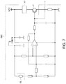
- FIG. 7 is a diagram showing a configuration example of a temperature control circuit.
- FIG. 8 is a graph showing a temperature change, due to an outside air temperature, of the resonator module accommodated in the oscillator according to the first embodiment.
- FIG. 9 is a graph showing a simulation result of a stress generated in amount portion of a resonator element of the resonator module when shock is applied thereto.
- FIG. 10 is a sectional view of an oscillator according to a second embodiment.
- FIG. 11 is a plan view of the oscillator according to the second embodiment.
- FIG. 12 is a sectional view of an oscillator according to a third embodiment.
- FIG. 13 is a sectional view of an oscillator according to a fourth embodiment.
- FIG. 14 is a perspective view showing a digital still camera that is an electronic device.
- the Z-axis matches a thickness direction of an oscillator, in other words, a direction in which a base and a cap joined to the base are arranged.
- the Z-axis is a direction that matches a direction in which the base, a resonator module accommodated in an accommodation space formed by the base and the cap, and a first substrate are arranged, and is a direction that matches a direction perpendicular to a surface to which a lead terminal that supports an oscillation circuit unit of the first substrate or the resonator module is connected.
- the X-axis and the Y-axis are orthogonal to each other in a virtual surface that includes a surface to which the oscillation circuit unit of the first substrate is connected.
- the X-axis extends along a direction in which lead terminals that are arranged in two rows face each other
- the Y-axis extends along an arrangement direction of the lead terminals and an arrangement direction of pin terminals that support the first substrate.
- a direction parallel to the X-axis is referred to as an “X-axial direction”
- a direction parallel to the Y-axis is referred to as a “Y-axial direction”
- a direction parallel to the Z-axis is referred to as a “Z-axial direction”.
- a direction directing from the base to the first substrate along the Z-axis is referred to as a +Z-axial direction
- a direction opposite to the +Z-axial direction is referred to as a ⁇ Z-axial direction.
- a surface on a side of the +Z-axial direction is set as an upper surface
- a surface on a side of the ⁇ Z-axial direction is set as a lower surface.
- interconnect patterns or electrode pads (terminal electrodes) formed inside a case that includes the base are not shown in the drawings.
- FIG. 1 is a sectional view of the oscillator according to the first embodiment.
- FIG. 2 is a plan view of the oscillator according to the first embodiment. In FIG. 2 , for ease of description, a perspective view of a cap is shown.
- FIG. 3 is a sectional view showing a resonator module and a lead terminal accommodated in the oscillator.
- FIG. 4 is a view seen from P in FIG. 3 showing the resonator module and the lead terminal.
- FIGS. 5A to 5D are process diagrams showing an example of a forming process of a lead terminal, in which FIG. 5A is a first process diagram, FIG.
- FIG. 5B is a second process diagram
- FIG. 5C is a third process diagram
- FIG. 5D is a fourth process diagram.
- FIG. 6 is a functional block diagram of the oscillator.
- FIG. 7 is a diagram showing a configuration example of a temperature control circuit.
- An oscillator 1 is an oven controlled crystal oscillator (OCXO).
- the oscillator 1 includes a case 10 that includes a base 101 and a cap 102 joined to the base 101 , a base substrate 30 that is a second substrate provided on a side of a lower surface 101 r of the base 101 , and a regulator 40 mounted on an upper surface 30 f of the base substrate 30 , as shown in FIGS. 1 and 2 .
- the case 10 has an accommodation space (cavity) S 1 that is formed by the base 101 and the cap 102 that is provided along an outer periphery of the base 101 and is joined to an upper surface (surface on the +Z-axis side) of a flange 101 b that is recessed from an upper surface 101 f of the base 101 .
- a heater 7 is connected, on a side of the base 101 , to the resonator module 2 disposed in the accommodation space S 1 , and an oscillation circuit element 4 that includes an oscillation circuit of the resonator module 2 is connected, on a side of the resonator module 2 , to the circuit board 8 .
- the respective components that is, the heater 7 connected to the resonator module 2 , the resonator module 2 connected to the circuit board 8 through the lead terminals 12 , the oscillation circuit element 4 connected to the circuit board 8 , and the circuit board 8 are sequentially disposed in the accommodation space S 1 .
- the base 101 that forms the case 10 is formed of a material such as Kovar, soft iron, or iron nickel, and is provided with the flange 101 b in the outer peripheral portion. Further, in the base 101 , a plurality of through holes that penetrate from an upper surface 101 f to a lower surface 101 r are provided, and the conductive pin terminal 14 is inserted into each through hole. Each pin terminal 14 is formed of a hermetic terminal, and a gap between the through hole and the pin terminal 14 is air-tightly sealed by the sealing member 103 such as glass. Further, stand-offs 13 formed of an insulator such as glass may be provided on the lower surface 101 r of the base 101 .
- the pin terminal 14 is an introduction terminal that is formed of a pin member such as Kovar, soft iron, or iron nickel and electrically connects the inside and the outside of the accommodation space S 1 . Further, the pin terminal 14 has one end on the side of the lower surface 101 r of the base 101 and the other end on the side of the accommodation space S 1 , and is erected along the Z-axial direction. Further, the pin terminals 14 are arranged in two rows along the Y-axial direction. In this embodiment, a row of four pin terminals 14 arranged in the +X-axial direction and a row of five pin terminals 14 arranged in the ⁇ X-axial direction are provided, but the number of arrangements or the number of pin terminals does not matter.
- a row of four pin terminals 14 arranged in the +X-axial direction and a row of five pin terminals 14 arranged in the ⁇ X-axial direction are provided, but the number of arrangements or the number of pin terminals does not matter.
- the cap 102 that forms the case 10 is provided by forming a thin plate of a metallic material such as nickel silver, Kovar, soft iron or iron nickel through pressing, raising, or the like in a recessed shape, and includes an outer peripheral portion 102 f formed by bending outward an opening portion thereof in a flange shape.
- the case 10 has a configuration in which the accommodation space (cavity) S 1 is formed by mounting the outer peripheral portion 102 f of the cap 102 to overlap the flange 101 b of the base 101 and air-tightly joining (air-tightly sealing) a portion Q in which the flange 101 b and the outer peripheral portion 102 f overlap each other using, for example, a resistance welding process, or the like.
- the accommodation space S 1 is air-tightly sealed to have a reduced pressure atmosphere of a pressure lower than the atmospheric pressure (which may be referred to as vacuum), or an inert gas atmosphere of nitrogen, argon, or helium.
- the inside of the accommodation space S 1 is not easily affected by an outside air temperature, and thus, it is possible to enhance the accuracy of temperature control of the resonator module 2 disposed in the accommodation space S 1 .
- the circuit board 8 that is the first board may be configured of a printed circuit board (PCB), for example.
- the circuit board 8 is formed in a rectangular shape in a plan view seen in the Z-axial direction, and is formed with through holes at positions that face positions where the pin terminals 14 fixed to the base 101 are erected.
- the circuit board 8 is fixed to the pin terminals 14 in a state where the ends of the pin terminals 14 on the side of the accommodation space S 1 are inserted in the through holes.
- the circuit board 8 includes a lower surface 8 r that is a first surface that is a surface on the side of the base 101 , and an upper surface 8 f that is a second surface that is a surface opposite to the lower surface 8 r.
- circuit patterns of circuit interconnects, terminals, or the like are provided on the upper surface 8 f that is the second surface and the lower surface 8 r that is the first surface of the circuit board 8 . Further, for example, a digital to analog (D/A) conversion element 5 , a temperature sensor 15 , a different electronic element 16 , and the like are connected to the circuit pattern on the upper surface 8 f of the circuit board 8 .
- D/A digital to analog
- the plurality of lead terminals 12 that support the resonator module 2 and the oscillation circuit element 4 that includes the oscillation circuit of the resonator module 2 are connected to the circuit pattern of the lower surface 8 r on the circuit board 8 .
- the lead terminals 12 are connected in connection regions R 2 that are positioned on outer peripheral sides of the circuit board 8 and are respectively arranged along two rows in which the pin terminals 14 are connected. In this way, as the lead terminals 12 are connected to the lower surface 8 r of the circuit board 8 , the lead terminals 12 are disposed between the circuit board 8 and the base 101 , and thus, the lead terminals are not easily affected by the outside air temperature through the cap 102 .
- the oscillation circuit element 4 is disposed at an intermediate position between two rows in which the lead terminals 12 are connected, in other words, is positioned at a central portion of the circuit board 8 , and is provided at a position that faces the resonator module 2 (which will be described later) supported by the lead terminals 12 .
- the resonator module 2 includes a package 20 having a package base 21 and a lid 22 joined to the package base 21 , and a resonator element 3 accommodated in the package 20 .
- the package 20 includes the package base 21 to which the resonator element 3 is mounted, the lid 22 that provides an accommodation space S 2 between the lid 22 and the package base 21 to accommodate the resonator element 3 and is joined to the package base 21 , and a frame-shaped sealing 23 that is positioned between the package base 21 and the lid 22 and through which the package base 21 and the lid 22 are joined to each other.
- the package base 21 has a cavity shape having a recess 25 that is opened in the +Z-axial direction, and has a rectangular shape that is an approximately square shape in an outline shape, in a plan view seen in the Z-axial direction.
- the outline shape of the package base 21 is not limited to the approximately square shape, and may be a different rectangular shape.
- a direction directing from the bottom of the package base 21 toward the opening thereof along the Z-axis is set as the +Z-axial direction
- a direction directing from the opening of the package base 21 toward the bottom thereof along the Z-axis direction is set as the ⁇ Z-axial direction.
- the recess 25 includes a first step that is opened in the +Z-axial direction of the package base 21 and a second step that is opened at the bottom of the first step.
- the resonator element 3 is fixed to an internal terminal (not shown) provided at an end portion of the package base 21 through a conductive fixing member 29 such as a conductive adhesive, for example.
- a quartz crystal board 31 that forms the resonator element 3 is obtained by forming an SC cut quartz crystal board into a planar shape of an approximately circular shape (not shown) through machining, or the like. By using the SC cut quartz crystal board, the resonator element 3 in which a frequency gap or a resistance increase due to spurious vibration is small and a temperature characteristic is also stable is obtained.
- the planar shape of the quartz crystal board 31 is not limited to the circular shape, and may be a non-linear shape such as an oval shape or an elliptical shape, or may be a linear shape such as a triangular shape or a rectangular shape.
- a non-linear shape such as an oval shape or an elliptical shape
- a linear shape such as a triangular shape or a rectangular shape.
- the resonator element 3 is not limited to the SC cut, and instead, may employ a quartz crystal resonator of an AT cut or a BT cut, a surface acoustic wave (SAW) resonator, or the like, for example. Further, as the resonator element 3 , instead of the quartz crystal resonator, for example, a piezoelectric resonator, a micro electro mechanical systems (MEMS) resonator, or the like may be used.
- MEMS micro electro mechanical systems
- a piezoelectric single crystal material such as quartz crystal, lithium tantalate, or lithium niobate
- a piezoelectric material such as piezoelectric ceramics such as lead zirconate titanate, a silicon semiconductor material, or the like
- excitation means of the resonator element 3 may use a piezoelectric effect, or may use an electrostatic drive due to a Coulomb force.
- the lid 22 has a plate shape, and is joined to an end face of the package base 21 on the +Z-axis side through the sealing 23 to block the opening of the recess 25 .
- the sealing 23 is disposed in a frame shape, and is disposed between the end face of the package base 21 on the +Z-axis side and the lid 22 .
- the sealing 23 is formed of a metallic material, and as the sealing 23 is melt, the package base 21 and the lid 22 are air-tightly joined to each other. In this way, as the opening of the recess 25 is blocked by the lid 22 , the second accommodation space (second cavity) S 2 is formed, and thus, it is possible to accommodate the resonator element 3 in the second accommodation space S 2 .
- the air-tightly sealed second accommodation space S 2 of the package 20 is in a reduced pressure state (for example, about 10 Pa or smaller).
- a reduced pressure state for example, about 10 Pa or smaller.
- the atmosphere of the second accommodation space S 2 is not particularly limited, and for example, may be filled with an inert gas such as nitrogen or argon to form an atmospheric pressure.
- a component material of the package base 21 is not particularly limited, and for example, may employ various types of ceramics such as aluminum oxide.
- the package base 21 may be manufactured by sintering a laminated body of ceramic sheets (green sheets).
- a component material of the lid 22 is not particularly limited, and may employ a member having a linear expansion coefficient similar to that of the component material of the package base 21 and approximate.
- the component material of the lid 22 is a metallic material (for example, an alloy such as Kovar).
- first connection terminals 24 and second connection terminals 26 that are electrically connected to the resonator element 3 using an internal interconnect (not shown) are provided.
- first connection terminals 24 are arranged along an outer edge disposed on the side of the +X-axial direction
- second connection terminals 26 are arranged along an outer edge disposed on the opposite side of the ⁇ X-axial direction.
- the number of first connection terminals 24 and the number of second connection terminals 26 are not particularly limited, and may be arbitrarily set.
- the first connection terminals 24 and the second connection terminals 26 may be formed, for example, using a method for sintering a metallic interconnect material such as tungsten (W) or molybdenum (Mo) on the lower surface 21 r of the package base 21 through screen printing and performing plating of nickel (Ni), gold (Au), or the like thereon.
- a metallic interconnect material such as tungsten (W) or molybdenum (Mo)
- Mo molybdenum
- the lower surface 21 r of the package base 21 may be referred to as the lower surface 21 r of the resonator module 2 as necessary.
- a second connection portion 12 a of the lead terminal 12 is electrically connected and fixed to each of the first connection terminals 24 and the second connection terminals 26 that are provided on the lower surface 21 r of the resonator module 2 , for example, using a conductive adhesive, soldering, or the like.
- the resonator module 2 is supported in a so-called suspended state on the circuit board 8 through the lead terminals 12 in a state where first connection portions 12 d of the lead terminals 12 are electrically connected and fixed to the lower surface 8 r of the circuit board 8 .
- Each lead terminal 12 includes the second connection portion 12 a provided at a position that includes one end thereof, the first connection portion 12 d provided at a position that includes the other end thereof, and a first extension portion 12 b and a second extension portion 12 c that are positioned between the second connection portion 12 a and the first connection portion 12 d and are connected to each other at a second bending portion B 2 . Further, the second connection portion 12 a and the first extension portion 12 b are connected to each other at a first bending portion B 1 , and the first connection portion 12 d and the second extension portion 12 c are connected to each other at a third bending portion B 3 .
- the lead terminal 12 includes three bending portions of the first bending portion B 1 , the second bending portion B 2 , and the third bending portion B 3 between the second connection portion 12 a connected to the resonator module 2 and the first connection portion 12 d.
- each lead terminal 12 includes the second connection portion 12 a provided at the position including one end thereof, the first extension portion 12 b that extends from the second connection portion 12 a and is bent in a direction of being gradually spaced from the resonator module 2 at the first bending portion B 1 , the second extension portion 12 c that extends from the first extension portion 12 b and is bent in a direction of being gradually close to the resonator module 2 at the second bending portion B 2 , and the first connection portion 12 d that extends from the second extension portion 12 c and is bent that is approximately parallel to the lower surface 21 r of the package base 21 that forms the resonator module 2 at the third bending portion B 3 .
- the lead terminal 12 has a configuration in which the second connection portion 12 a is connected to the first connection terminal 24 and the second connection terminal 26 of the resonator module 2 and the first connection portion 12 d is connected to the lower surface 8 r of the circuit board 8 while protruding at the second bending portion B 2 in an outward direction with a gap with respect to an outer side surface of the resonator module 2 .
- the three bending portions of the first bending portion B 1 , the second bending portion B 2 , and the third bending portion B 3 are provided in the lead terminal 12 between the second connection portion 12 a connected to the resonator module 2 and the first connection portion 12 d connected to the circuit board 8 , and the resonator module 2 is supported in a so-called suspended state with respect to the circuit board 8 , and thus, it is possible to easily generate deflection in the lead terminal 12 .
- the lead terminal 12 is configured to protrude at the second bending portion B 2 in the outward direction of the resonator module 2 , it is possible to weaken stiffness of the lead terminal 12 , and to effectively absorb shock or the like applied to the resonator module 2 from the circuit board 8 .
- the lead terminal 12 is configured so that the first connection portion 12 d of the lead terminal 12 connected to the circuit board 8 , in a plan view in a direction where the resonator module 2 and the circuit board 8 are arranged, that is, in the +Z-axial direction is disposed outside with reference to the contour of the resonator module 2 .
- the first connection portion 12 d of the lead terminal 12 connected to the circuit board 8 is disposed outside with reference to the contour of the resonator module 2 , in a plan view as described above, it is possible to easily visually recognize the first connection portion 12 d of the lead terminal 12 from the side of the resonator module 2 , and to easily confirm a connection state.
- a configuration in which four lead terminals 12 are disposed on the side of the first connection terminals 24 of the resonator module 2 and four lead terminals 12 are disposed on the side of the second connection terminals 26 is shown, but the number of the lead terminals 12 is not limited thereto. Any number of lead terminals 12 that is able to support the resonator module 2 may be used. Further, the lead terminal 12 may be formed in processes shown in FIGS. 5A to 5D , for example.
- a lead frame in which terminals 12 L corresponding to the lead terminals 12 (see FIG. 3 ) are continuously connected to a frame is prepared, and one end portion of each of the terminals 12 L continuously connected to the lead frame is connected to the lower surface 21 r of the resonator module 2 to which the heater 7 is connected.
- a part that includes one end portion of each of the terminals 12 L continuously connected to the lead frame and connected to the resonator module 2 corresponds to the second connection portion 12 a of the lead terminal 12 after formation.
- the third bending portion B 3 is formed in a tip portion of the terminal 12 L using pressing or the like, and the first connection portion 12 d is formed by bending the terminal 12 L inward at a predetermined angle.
- the predetermined angle is set so that the first connection portion 12 d is approximately parallel to the lower surface 21 r of the resonator module 2 when bending in a fourth process (which will be described later) is performed.
- the second bending portion B 2 is formed in a central portion of the terminal 12 L using pressing or the like, and the second extension portion 12 c is formed by bending the terminal 12 L inward at a predetermined angle.
- the first bending portion B 1 is formed in a portion of the terminal 12 L adjacent to the resonator module 2 using pressing or the like, and the first extension portion 12 b and the second connection portion 12 a are formed by bending the terminal 12 L further inward at a predetermined angle. Further, although not shown, by separating the portions of the terminal 12 L formed in the above-described processes from the lead frame, it is possible to form the lead terminal 12 in a state of being connected to the resonator module 2 .
- the oscillation circuit element 4 at least includes an oscillation circuit 530 (see FIG. 6 ) that is an oscillation circuit that oscillates the resonator module 2 , and is disposed between the resonator module 2 and the circuit board 8 . At least a part of the oscillation circuit element 4 may be included between the resonator module 2 and the circuit board 8 .
- the oscillation circuit element 4 is disposed as described above, since the oscillation circuit element 4 is disposed to be close to the resonator module 2 compared with a case where the oscillation circuit element 4 is disposed at a side of the circuit board 8 opposite to the resonator module 2 , it is possible to easily make the temperature of the oscillation circuit element 4 close to the temperature of the resonator module 2 . Accordingly, it is possible to suppress reduction in frequency accuracy due to a temperature difference between the oscillation circuit element 4 and the resonator module 2 .
- the heater 7 is an electronic component having a so-called “constant temperature function”, which is connected to the lower surface 21 r that is the surface of the resonator module 2 on the side of the base 101 , heats the oscillation circuit element 4 through the resonator element 3 of the resonator module 2 or the resonator module 2 , and maintains the temperatures of the resonator module 2 (resonator element 3 ) and the oscillation circuit element 4 approximately uniformly.
- Constant temperature function which is connected to the lower surface 21 r that is the surface of the resonator module 2 on the side of the base 101 , heats the oscillation circuit element 4 through the resonator element 3 of the resonator module 2 or the resonator module 2 , and maintains the temperatures of the resonator module 2 (resonator element 3 ) and the oscillation circuit element 4 approximately uniformly.
- the temperature of the resonator element 3 it is preferable to control the temperature of the resonator element 3 to be close to a peak temperature (which varies as specifications, for example, about 70° C. to about 100° C.) indicating a zero temperature coefficient.
- a peak temperature which varies as specifications, for example, about 70° C. to about 100° C.
- the heater 7 is connected to the lower surface 21 r that is the surface of the resonator module 2 on the side of the base 101 , in other words, as the resonator module 2 is disposed between the heater 7 and the circuit board 8 , heat of the resonator module 2 hardly escapes, and the resonator module is less effected by the influence of the outside air temperature. Thus, it is possible to enhance accuracy of temperature control of the resonator module 2 .
- the D/A conversion element 5 connected to the circuit board 8 includes a reference voltage generation circuit 570 , a D/A conversion circuit 580 , a digital interface circuit 590 , and the like shown in FIG. 6 , processes a signal input through an external terminal 1 a of the oscillator 1 , and outputs a frequency-controlled signal.
- the D/A conversion element 5 may have a configuration in which a part of these components is omitted or modified or other components are added thereto.
- the temperature sensor 15 connected to the circuit board 8 is disposed in the vicinity of the resonator module 2 , and detects the temperature (temperature of a thermostatic chamber) of the resonator module 2 .
- a thermistor a negative temperature coefficient (NTC) thermistor, a positive temperature coefficient (PTC) thermistor, or the like
- a platinum resistance a platinum resistance, or the like
- the base substrate 30 that is the second substrate provided on the side of the lower surface 101 r of the base 101 may be configured of a printed circuit board (PCB), for example.
- the base substrate 30 includes an upper surface 30 f disposed on the size of the base 101 and a lower surface 30 r that is a surface opposite to the upper surface.
- the base substrate 30 is provided with a bottomed hole 34 on the upper surface 30 f that faces at a position where each pin terminal 14 fixed to the base 101 is erected.
- the base substrate 30 is connected to the pin terminal 14 using a joining material 33 such as soldering in a state where one end of the pin terminal 14 is inserted into the bottomed hole 34 .
- the regulator 40 is connected to the upper surface 30 f of the base substrate 30 .
- a plurality of external connection terminals 32 are provided on the lower surface 30 r of the base substrate 30 .
- the regulator 40 that is connected to the upper surface 30 f of the base substrate 30 has a function of a voltage regulator that smoothens an input DC power and outputs the result as a constant voltage, and adjusts a power supply voltage supplied to the heater 7 to become constant.
- the regulator 40 may output a constant voltage even though an input voltage or an output current is changed.
- the oscillator 1 includes the resonator module 2 , the D/A conversion element 5 , the oscillation circuit element 4 including an oscillation circuit, a variable capacitance element 507 , a variable capacitance element 508 , the heater 7 that is a temperature control element, and the temperature sensor 15 .
- the oscillator 1 of this embodiment may have a configuration in which a part of the components shown in FIG. 6 is omitted or modified or other components are added thereto.
- the D/A conversion element 5 may be configured to include the reference voltage generation circuit 570 , the D/A conversion circuit 580 , and the digital interface circuit 590 .
- the D/A conversion element 5 may have a configuration in which a part of the components is omitted or modified or other components are added thereto.
- the digital interface circuit 590 is electrically connected to the external terminal 1 a of the oscillator 1 , acquires a signal (a signal including digital data for controlling the frequency of the oscillation circuit 530 ) input from the external terminal 1 a , converts the signal into an N-bit data signal, and outputs the result to the D/A conversion circuit 580 .
- the reference voltage generation circuit 570 generates a high potential reference voltage VDH and a low potential reference voltage VDL of the D/A conversion circuit 580 based on a power supply voltage VCC supplied from the outside (the outside of the oscillator 1 ) of the D/A conversion circuit 5 .
- the D/A conversion circuit 580 generates a frequency control signal for converting a digital signal input through the digital interface circuit 590 into an analog signal to control the frequency of the oscillation circuit 530 .
- the D/A conversion circuit 580 receives an input of an N-bit data signal (digital data for controlling the frequency of the oscillation circuit 530 ) output from the digital interface circuit 590 , and converts the N-bit data signal into an analog signal of a voltage between the high potential reference voltage VDH and the low potential reference voltage VDL, and outputs the result.
- various types such as a resistance division type (which may be referred to as a voltage distribution type, a resistance string type, or a voltage potentiometer type), a resistance ladder type (an R-2R ladder type, or the like), a capacitance array type, or a delta-sigma type that are well known may be used.
- a resistance division type which may be referred to as a voltage distribution type, a resistance string type, or a voltage potentiometer type
- a resistance ladder type an R-2R ladder type, or the like
- a capacitance array type or a delta-sigma type that are well known
- a voltage (control voltage) VC of an analog signal output from the D/A conversion circuit 580 is applied to the variable capacitance element 508 outside the D/A conversion circuit 5 , and a capacitance value of the variable capacitance element 508 is changed according to the control voltage VC.
- the variable capacitance element 508 may be a varicap diode (varactor) in which a capacitance value is changed according to the control voltage VC applied to one end thereof, for example.
- the oscillation circuit element 4 includes a temperature compensation circuit 510 , a temperature sensor 513 , an oscillation circuit 532 , a temperature control circuit 560 , a reference voltage generation circuit 572 , a digital interface circuit 592 , and a storage 600 .
- the oscillation circuit element 4 is an integrated circuit (IC), or the like, for example.
- the oscillation circuit element 4 may have a configuration in which a part of the components is omitted or modified or other components are added thereto.
- the temperature compensation circuit 510 is connected to the temperature sensor 513 , and generates a temperature compensation voltage TC for correcting frequency-temperature characteristics of an output signal of the oscillation circuit 530 according to an output signal of the temperature sensor 513 .
- the temperature sensor 513 outputs a voltage based on an ambient temperature, for example.
- the temperature sensor 513 may be a positive polarity sensor in which an output voltage is higher as the temperature is higher, or may be a negative polarity sensor in which an output voltage is lower as the temperature is higher.
- a temperature compensation voltage TC output from the temperature compensation circuit 510 is applied to the variable capacitance element 507 outside the oscillation circuit element 4 , and a capacitance value of the variable capacitance element 507 is changed according to the temperature compensation voltage TC.
- the variable capacitance element 507 may be a varicap diode (varactor) in which a capacitance value is changed according to the temperature compensation voltage TC applied to one end thereof, for example.
- the oscillation circuit 532 forms the oscillation circuit 530 that oscillates the resonator module 2 together with the variable capacitance element 507 , the variable capacitance element 508 , and other electronic components (not shown) externally attached to a terminal of the oscillation circuit element 4 . That is, in this embodiment, the oscillation circuit element 4 includes the oscillation circuit 532 that is a part of the oscillation circuit 530 , but the oscillation circuit element 4 may be configured to have at least a part of the oscillation circuit 530 , for example, to have the entirety of the oscillation circuit 530 .
- the oscillation circuit 530 oscillates the resonator module 2 at a frequency based on the capacitance value of the variable capacitance element 507 and the capacitance value of the variable capacitance element 508 , and outputs an oscillation signal VO.
- the oscillation signal VO output from the oscillation circuit 530 is output to the outside (the outside of the oscillator 1 ) of the oscillation circuit element 4 .
- the temperature control circuit 560 is disposed in the vicinity of the resonator module 2 , and controls an operation of the heater 7 for controlling the temperature of the resonator module 2 based on an output voltage of the temperature sensor 15 that detects the temperature (temperature of the thermostatic chamber) of the resonator module 2 . Specifically, the temperature control circuit 560 controls the operation of the heater 7 to uniformly maintain the temperature of the resonator module 2 according to the output voltage of the temperature sensor 15 .
- a heater element a power transistor, a resistor, or the like
- a heat absorbing element a Peltier element, or the like
- the reference voltage generation circuit 572 generates a power supply voltage VA of the oscillation circuit 530 , a reference voltage VREF 1 of the temperature compensation circuit 510 , a reference voltage VREF 2 of the temperature control circuit 560 , or the like, based on the power supply voltage VCC supplied from the outside (the outside of the oscillator 1 ) of the oscillation circuit element 4 .
- the storage 600 stores information based on a digital signal input through the digital interface circuit 592 .
- the storage 600 includes a non-volatile memory (not shown) and a register (not shown), and setting information or the like of the temperature compensation circuit 510 is stored in the non-volatile memory.
- the non-volatile memory may be realized by a flash memory such as a metal-oxide-nitride-oxide-silicon (MONOS) memory, an electrically erasable programmable read-only memory (EEPROM), or the like, for example.
- MONOS metal-oxide-nitride-oxide-silicon
- EEPROM electrically erasable programmable read-only memory
- Each piece of setting information stored in the non-volatile memory is transmitted to the register from the non-volatile memory in a case where power is supplied to the oscillation circuit element 4 (in a case where the power supply voltage VCC increases from 0V to a desired voltage), and is maintained in the register. Further, each piece of setting information maintained in the register is supplied to the temperature compensation circuit 510 , or the like.
- the digital interface circuit 592 is electrically connected to the external terminal 1 b different from the external terminal 1 a of the oscillator 1 , acquires a signal input through the external terminal 1 b , and performs reading and writing with respect to the storage 600 (the non-volatile memory and the register).
- the digital interface circuit 592 may be, for example, an interface circuit corresponding to an inter-integrated circuit (I 2 C) bus, or an interface circuit corresponding to a serial peripheral interface (SPI).
- FIG. 7 is a diagram showing a configuration example of the temperature control circuit 560 .
- a NPN-type power transistor is used as the heater 7
- an NTC thermistor is used as the temperature sensor 15 .
- a resistance value of the temperature sensor 15 increases, and an input potential difference of an operational amplifier increases.
- an output voltage of the operational amplifier is proportional to an input potential difference.
- the heater 7 NPN-type power transistor
- the operation of the heater 7 is controlled so that the resistance value of the temperature sensor 15 becomes a desired value, that is, so that a desired temperature is maintained.
- An internal temperature of the thermostatic chamber is controlled to be maintained as a desired temperature (for example, in a case where the resonator module 2 is a SC cut quartz crystal resonator, a temperature that becomes a peak of an upward projection in a three-dimensional curve of a frequency temperature characteristic), by the temperature control circuit 560 , based on the frequency temperature characteristic of the output signal of the oscillation circuit 530 determined according to the temperature characteristic of the resonator module 2 or the oscillation circuit element 4 .
- a desired temperature for example, in a case where the resonator module 2 is a SC cut quartz crystal resonator, a temperature that becomes a peak of an upward projection in a three-dimensional curve of a frequency temperature characteristic
- the regulator 40 having a function of a voltage regulator that adjusts the power supply voltage supplied to the heater 7 to become uniform is provided between the temperature control circuit 560 and the heater 7 . Since the regulator 40 is able to output a constant voltage even though an input voltage or an output current is changed, it is possible to reduce a variation of the power supply voltage applied to the heater 7 , and to reduce a temperature variation of the heater 7 due to the variation of the power supply voltage.
- the resonator module 2 is supported with a gap with respect to the circuit board 8 between the circuit board 8 and the base 101 through the lead terminal 12 connected to the circuit board 8 accommodated in the case 10 configured of the base 101 and the cap 102 .
- the resonator module 2 is supported in a so-called suspended state between the circuit board 8 and the base 101 through the lead terminal 12 .
- the resonator module 2 As described above, as the resonator module 2 is supported in the suspended state between the base 101 and the circuit board 8 , components such as the resonator module 2 , the heater 7 , or the oscillation circuit element 4 are easily and tightly disposed in a space between the base 101 and the circuit board 8 , compared with a case where the resonator module 2 has a double-decker structure, and thus, it is possible to achieve miniaturization. Further, in the case of the same size as that of the double-decker structure, it is possible to secure a room in the space between the base 101 and the circuit board 8 to obtain the freedom of design for enhancement of performance.
- the accommodation space (cavity) S 1 that accommodates components such as the resonator module 2 or the oscillation circuit element 4 is air-tightly sealed by the base 101 and the cap 102 , it is possible to enhance the function of the thermostatic chamber in the accommodation space (cavity) S 1 . That is, it is possible to control accuracy of an oscillation characteristic generated as a control temperature of the resonator module 2 or the oscillation circuit element 4 in the accommodation space (cavity) S 1 is affected by the outside air temperature outside the cap 102 .
- FIG. 8 is a graph showing a temperature change, due to the outside air temperature, of the resonator module 2 accommodated in the oscillator 1 according to the first embodiment.
- the oscillator 1 of this embodiment is referred to as an air-tight type
- an oscillator that has the related-art so-called double-decker structure and is not air-tightly sealed that is a comparison target is referred to as an open-type.
- the temperature of the resonator module 2 gradually decreases to show a temperature variation of 3° C. between ⁇ 40° C. to +70° C. This occurs since the temperature control of the heater 7 that controls the temperature of the resonator module 2 is not performed as expected. That is, in the oscillator (open-type) of the related-art so-called double-decker structure, since cooperation between the temperature sensor 15 and the temperature control circuit 560 that are provided therein is not sufficiently achieved, the control temperature is easily affected by the influence of the outside air temperature intruded in the accommodation space S 1 .
- the temperature control circuit 560 over-reacts with respect to the outside air temperature, or contrarily, under-reacts therewith. Specifically, it is considered that the power supply power applied to the heater 7 becomes excessive in a case where the outside air temperature is low, and contrarily, the power supply power applied to the heater 7 becomes too small in a case where the outside air temperature is high, and thus, the above-described phenomenon occurs.
- the temperature of the resonator module 2 also tends to increase as the outside air temperature increases, in which the temperature variation is a small value of only 0.5° C. between ⁇ 40° C. and +70° C., which is a temperature variation of about 1 ⁇ 6 compared with that in the related-art oscillator.
- the temperature variation of the resonator module 2 is small. It is considered that this is because since there is no intrusion of outside air into the accommodation space (cavity) S 1 , the influence of the outside air temperature is small, and thus, the temperature control of the heater 7 that controls the temperature of the resonator module 2 is performed as expected.
- the lead terminal 12 that supports the resonator module 2 in the suspended state extends from a connection portion with respect to the circuit board 8 disposed in the connection region R 2 to a connection portion disposed in the connection region R 1 of the lower surface 21 r of the resonator module 2 on the side opposite to the circuit board 8 , it is possible to set the length to be sufficiently long.
- the lead terminal 12 has the swelling portion at the second bending portion B 2 in the outward direction of the resonator module 2 by three bending portions of the first bending portion B 1 , the second bending portion B 2 , and the third bending portion B 3 , it is possible to weaken the stiffness of the lead terminal 12 .
- deflection of the lead terminal 12 easily occurs, and shock is absorbed by the deflection of the lead terminal 12 .
- FIG. 9 is a graph showing a simulation result of stress generated in amount portion (a joining portion with respect to the package base 21 ) of the resonator element 3 of the resonator module 2 when shock is applied to the oscillator 1 .
- the oscillator 1 of this embodiment is referred to as an air-tight type, and an oscillator of the related-art so-called double-decker structure that is a comparison target is referred to as an open-type.
- the resonator module 2 is supported by the long lead terminal 12 , it is possible to lengthen a distance to the cap 102 that is in contact with outside air, disposed on the side of the circuit board 8 , the circuit board 8 , or the like, and to reduce the influence due to the outside air temperature on the resonator module 2 .
- the oscillator 1 having a good temperature control with excellent impact resistance with respect to the resonator module 2 without increasing its external shape.
- FIG. 10 is a sectional view of the oscillator according to the second embodiment.
- FIG. 11 is a plan view of the oscillator according to the second embodiment.
- configurations different from those of the first embodiment will be mainly described. Further, in the respective drawings, the same reference numerals are given to the same configurations, and description thereof may not be repeated.
- An oscillator 1 A of the second embodiment shown in FIGS. 10 and 11 is the same as the oscillator 1 of the above-described first embodiment except that a position of a connection portion with respect to a circuit board 8 A of a lead terminal 121 that supports (suspends) a resonator module 2 accommodated in an accommodation space (cavity) S 1 is changed.
- the lead terminal 121 and the circuit board 8 A that are different configurations will be mainly described.
- the oscillator 1 A of this embodiment includes a case 10 that includes a base 101 and a cap 102 joined to the base 101 , a base substrate 30 that is a second substrate provided on a side of a lower surface 101 r of the base 101 , and a regulator 40 mounted on an upper surface 30 f of the base substrate 30 , as shown in FIG. 10 .
- the case 10 has an accommodation space (cavity) S 1 that is formed by the base 101 and the cap 102 that is provided along an outer periphery of the base 101 and is joined to an upper surface (a surface on the +Z-axis side) of a flange 101 b that is recessed from an upper surface 101 f of the base 101 . Since these components are the same as in the first embodiment, description thereof will not be repeated.
- a heater 7 is connected, on a side of the base 101 , to the resonator module 2 disposed in the accommodation space S 1 , and an oscillation circuit element 4 that includes an oscillation circuit of the resonator module 2 is connected, on a side of the resonator module 2 , to the circuit board 8 A.
- the respective components that is, the heater 7 connected to the resonator module 2 , the resonator module 2 connected to the circuit board 8 A through the lead terminals 121 , the oscillation circuit element 4 connected to the circuit board 8 A, and the circuit board 8 A are sequentially disposed in the accommodation space S 1 , from the side of the base 101 , in a plan view in the Y-axial direction.
- the components other than the lead terminal 121 and the circuit board 8 A for example, the resonator module 2 , the oscillation circuit element 4 , and the like are the same as in the first embodiment, description thereof will not be repeated.
- the circuit board 8 A that is the first substrate may be configured of a printed circuit board (PCB), for example.
- the circuit board 8 A is formed in a rectangular shape in a plan view seen in the Z-axial direction, and is formed with through holes at positions that face positions where the pin terminals 14 fixed to the base 101 are erected.
- the circuit board 8 A is fixed to the pin terminals 14 in a state where the ends of the pin terminals 14 on the side of the accommodation space S 1 are inserted in the through holes.
- the circuit board 8 A includes a lower surface 108 r that is a first surface that is a surface on the side of the base 101 , and an upper surface 108 f that is a second surface that is a surface opposite to the lower surface 108 r .
- the circuit board 8 A is configured so that a cut portion 109 is provided on an outer peripheral side of a connection region R 2 in which each lead terminal 121 that supports the resonator module 2 is connected.
- the lead terminal 121 penetrates and extends from the side of the lower surface 108 r toward the side of the upper surface 108 f.
- circuit patterns of circuit interconnects, terminals, and the like are provided on the upper surface 108 f that is the second surface of the circuit board 8 A and the lower surface 108 r that is the first surface thereof. Further, for example, a digital to analog (D/A) conversion element 5 , a temperature sensor 15 , a different electronic element 16 , and the like are connected to the circuit pattern on the upper surface 108 f of the circuit board 8 A.
- D/A digital to analog
- the plurality of lead terminals 121 that support the resonator module 2 and the oscillation circuit element 4 that includes an oscillation circuit of the resonator module 2 are connected to the circuit pattern of the upper surface 108 f on the circuit board 8 A.
- the lead terminals 121 are connected in the connection regions R 2 that are positioned inside the cut portion 109 on outer peripheral sides of the circuit board 8 A and are respectively arranged along two rows in which the pin terminals 14 are connected using connecting materials 110 such as soldering or a conductive adhesive.
- a second connection portion 12 a of the lead terminal 121 is electrically connected and fixed to each of the first connection terminals 24 and the second connection terminals 26 that are provided on the lower surface 21 r of the resonator module 2 , for example, using a conductive adhesive, soldering, or the like.
- the resonator module 2 is supported in a so-called suspended state on the circuit board 8 A through the lead terminals 121 in a state where first connection portions 12 d of the lead terminals 121 are electrically connected and fixed to the upper surface 108 f of the circuit board 8 A.
- Each lead terminal 121 includes the second connection portion 12 a provided at a position that includes one end thereof, the first connection portion 12 d provided at a position that includes the other end thereof, and a first extension portion 12 b and a second extension portion 12 c that are positioned between the second connection portion 12 a and the first connection portion 12 d and are connected to each other at a second bending portion B 2 . Further, the second connection portion 12 a and the first extension portion 12 b are connected to each other at a first bending portion B 1 , and the first connection portion 12 d and the second extension portion 12 c are connected to each other at a third bending portion B 3 .
- the lead terminal 121 includes three bending portions of the first bending portion B 1 , the second bending portion B 2 , and the third bending portion B 3 between the second connection portion 12 a connected to the resonator module 2 and the first connection portion 12 d.
- each lead terminal 121 includes the second connection portion 12 a provided at the position including one end thereof, the first extension portion 12 b that extends from the second connection portion 12 a and is bent in a direction of being gradually spaced from the resonator module 2 at the bending portion B 1 , the second extension portion 12 c that extends from the first extension portion 12 b and is bent in a direction of being gradually close to the resonator module 2 at the second bending portion B 2 , and the first connection portion 12 d that extends from the second extension portion 12 c and is bent that is approximately parallel to the lower surface 21 r of the package base 21 at the third bending portion B 3 .
- the lead terminal 121 has a configuration in which the second connection portion 12 a is connected to the first connection terminal 24 and the second connection terminal 26 of the resonator module 2 and the first connection portion 12 d is connected to the upper surface 108 f of the circuit board 8 A while passing inside the cut portion 109 of the circuit board 8 A while protruding at the second bending portion B 2 in an outward direction with a gap with respect to an outer surface of the resonator module 2 .
- the three bending portions of the first bending portion B 1 , the second bending portion B 2 , and the third bending portion B 3 are provided in the lead terminal 121 between the second connection portion 12 a connected to the resonator module 2 and the first connection portion 12 d connected to the circuit board 8 A and the resonator module 2 is supported in a so-called suspended state with respect to the circuit board 8 A, it is possible to easily cause the lead terminal 121 to be deflected.
- the lead terminal 121 is configured to protrude at the second bending portion B 2 in the outward direction of the resonator module 2 , it is possible to weaken stiffness of the lead terminal 121 , and to effectively absorb shock or the like transmitted to the resonator module 2 from the circuit board 8 A.
- the lead terminal 121 is connected to the upper surface 108 f of the circuit board on a side opposite to the base 101 , it is possible to prevent the lead terminal from being detached from the circuit board 8 A toward the base 101 .
- the lead terminal 121 is disposed to pass through the cut portion 109 of the circuit board 8 A, it is possible to easily perform positioning of the lead terminal 121 using a side surface of the cut portion 109 as a guide. In addition, it is possible to easily view a connection portion between the circuit board 8 A and the lead terminal 121 , and to easily confirm joining, in a plan view in the +Z-axial direction.
- the lead terminal 121 is configured so that the first connection portion 12 d of the lead terminal 121 connected to the circuit board 8 A, in a plan view in a direction where the resonator module 2 and the circuit board 8 A are arranged, that is, in the ⁇ Z-axial direction is disposed outside with reference to a contour of the resonator module 2 .
- the first connection portion 12 d of the lead terminal 121 connected to the circuit board 8 A is disposed outside with reference to the contour of the resonator module 2 , in the plan view, it is possible to easily view the first connection portion 12 d of the lead terminal 121 , and to easily confirm a connection state, from the side of the resonator module 2 (in the ⁇ Z-axial direction).
- a configuration in which four lead terminals 121 are disposed on the side of the first connection terminals 24 of the resonator module 2 and four lead terminals 121 are disposed on the side of the second connection terminals 26 is shown, but the number of the lead terminals 121 is not limited thereto. Any number of lead terminals 121 that is able to support the resonator module 2 may be used.
- the oscillator 1 A of to the second embodiment it is possible to obtain the same effects as those of the oscillator 1 in the first embodiment.
- the lead terminal 121 is connected to the upper surface 108 f of the circuit board on the side opposite to the base 101 , it is possible to prevent the lead terminal from being detached from the circuit board 8 A toward the base 101 .
- the lead terminal 121 is provided to pass through the cut portion 109 of the circuit board 8 A, it is possible to easily perform positioning of the lead terminal 121 using a side surface of the cut portion 109 .
- the lead terminal 121 may pass through an outer side of the outer periphery of the circuit board, and may be positioned using the outer peripheral side surface of the circuit board as a guide.
- FIG. 12 is a sectional view of the oscillator according to the third embodiment.
- configurations different from those of the first embodiment will be mainly described. Further, in the respective drawings, the same reference numerals are given to the same configurations, and description thereof may not be repeated.
- An oscillator 1 B according to the third embodiment shown in FIG. 12 is the same as the oscillator 1 according to the first embodiment except that a configuration of a case 200 including a base 201 is changed.
- the case 200 including the base 201 that is a different configuration will be mainly described.
- the oscillator 1 B includes the case 200 that includes the base 201 and a cap 102 joined to the base 201 , a base substrate 30 that is a second substrate provided on a side of a lower surface 101 r of the base 201 , and a regulator 40 mounted on an upper surface 30 f of the base substrate 30 .
- the case 200 has an accommodation space (cavity) S 1 that is formed by the base 201 and the cap 102 that is provided along an outer periphery of the base 201 and is joined to an upper surface (a surface on the +Z-axis side) of a flange 201 b that is recessed from an upper surface 101 f of the base 201 . Since the components other than the case 200 including the base 201 are the same as in the first embodiment, description thereof will not be repeated.
- a heater 7 is connected, on a side of the base 201 , to the resonator module 2 disposed in the accommodation space S 1 , and an oscillation circuit element 4 that includes an oscillation circuit of the resonator module 2 is connected, on a side of the resonator module 2 , to the circuit board 8 .
- the respective components that is, the heater 7 connected to the resonator module 2 , the resonator module 2 connected to the circuit board 8 through the lead terminals 12 , the oscillation circuit element 4 connected to the circuit board 8 , and the circuit board 8 are sequentially disposed in the accommodation space S 1 , from the side of the base 201 , in a sectional view in the Y-axial direction.
- these components for example, the resonator module 2 , the oscillation circuit element 4 , and the like are the same as in the first embodiment, description thereof will not be repeated.
- the base 201 that forms the case 200 is formed of a material such as Kovar, soft iron, or iron nickel, for example, and is provided with the flange 201 b in the outer peripheral portion. Further, in the base 201 , a plurality of through holes that penetrate from an upper surface 101 f to a lower surface 101 r are provided, and the conductive pin terminal 14 is inserted into each through hole. Each pin terminal 14 is formed of a hermetic terminal, for example, and a gap between the through hole and the pin terminal 14 is air-tightly sealed by the sealing member 203 such as glass. Further, stand-offs 13 formed of an insulator such as glass may be provided on the lower surface 101 r of the base 201 .
- a recess 202 that is recessed from the upper surface 101 f is provided in a central portion of the upper surface 101 f that is a surface on the resonator module 2 .
- the cap 102 that forms the case 200 is provided by forming a thin plate of a metallic material such as nickel silver, Kovar, soft iron or iron nickel through pressing, raising, or the like in a recessed shape, and includes an outer peripheral portion 102 f formed by bending outward an opening portion thereof in a flange shape.
- the case 200 has a configuration in which the accommodation space (cavity) S 1 is formed by mounting the outer peripheral portion 102 f of the cap 102 to overlap the flange 201 b of the base 201 and air-tightly joining (air-tightly sealing) a portion Q in which the flange 201 b and the outer peripheral portion 102 f overlap each other using, for example, a resistance welding process, or the like.
- the accommodation space S 1 is air-tightly sealed to have a reduced pressure atmosphere of a pressure lower than the atmospheric pressure (which may be referred to as vacuum), or an inert gas atmosphere of nitrogen, argon, or helium.
- the oscillator 1 B of the third embodiment it is possible to obtain the same effects as those of the oscillator 1 in the first embodiment.
- FIG. 13 is a sectional view of the oscillator according to the fourth embodiment.
- configurations different from those of the first embodiment will be mainly described. Further, in the respective drawings, the same reference numerals are given to the same configurations, and description thereof will not be repeated.
- An oscillator 1 C according to the fourth embodiment shown in FIG. 13 has a configuration in which the base substrate 30 that is the second substrate provided on the side of the lower surface 101 r of the base 101 that forms the oscillator 1 according to the first embodiment is removed.
- a configuration of a case 10 and components accommodated in an accommodation space S 1 of the case 10 are the same as in the oscillator 1 of the first embodiment.
- description of the same configurations as in the oscillator 1 of the first embodiment will not be repeated.
- the oscillator 1 C includes the case 10 that includes the base 101 and a cap 102 joined to the base 101 .
- the case 10 has the accommodation space (cavity) S 1 that is formed by the base 101 and the cap 102 that is provided along an outer periphery of the base 101 and is joined to an upper surface (a surface on the +Z-axis side) of a flange 101 b that is recessed from an upper surface 101 f of the base 101 .
- a heater 7 is connected, on a side of the base 101 , to the resonator module 2 disposed in the accommodation space S 1 , and an oscillation circuit element 4 that includes an oscillation circuit of the resonator module 2 is connected, on a side of the resonator module 2 , to the circuit board 8 .
- the respective components that is, the heater 7 connected to the resonator module 2 , the resonator module 2 connected to the circuit board 8 through the lead terminals 12 , the oscillation circuit element 4 connected to the circuit board 8 , and the circuit board 8 are sequentially disposed in the accommodation space S 1 , from the side of the base 101 , in a sectional view in the Y-axis direction.
- a regulator (not shown) that adjusts a power supply voltage of the heater 7 may be disposed.
- the oscillator 1 C of the fourth embodiment it is possible to obtain the same effects as those of the oscillator 1 of the first embodiment.
- the pin terminals 14 may be inserted and mounted in a printed circuit board such as an electronic device, for example.
- FIG. 14 is a perspective view showing a digital still camera that is an electronic device according to the invention. In the following description, an example using the oscillator 1 will be described.
- a display 1310 is provided on a rear surface of a case (body) 1302 in a digital still camera 1300 , and is configured to perform display based on an imaging signal of a CCD.
- the display 1310 functions as a finder that displays a subject as an electronic image.
- a light receiving unit 1304 that includes an optical lens (imaging optical system), a CCD, and the like is provided on a front surface side (in the figure, a rear surface side) of the case 1302 .
- an imaging signal of the CCD at that time point is transmitted to a memory 1308 for storage.
- an oscillator 1 is provided therein, and a controller 1316 is able to perform various controls relating to the digital still camera 1300 based on a highly accurate timing signal output from the oscillator 1 .
- the digital still camera 1300 that is such an electronic device has the oscillator 1 , it is possible to show the above-described effects of the oscillator 1 , and to achieve excellent reliability, particularly, an excellent temperature characteristic.
- the electronic device may be applied, in addition to the digital still camera 1300 shown in FIG. 14 , to an electronic device such as a personal computer, a portable phone, a smartphone, a tablet terminal, a timepiece (including Smart Watch), an ink jet type discharge device (for example, an ink jet printer), a lap-top personal computer, a TV, a wearable terminal such as a head mounted display (HMD), a video camera, a video tape recorder, a car navigation device, a pager, an electronic organizer (including a communication function), an electronic dictionary, an electronic calculator, an electronic game machine, a word processor, a workstation, a TV phone, a crime prevention TV monitor, electronic binoculars, a POS terminal, medical equipment (for example, an electronic clinical thermometer, a blood manometer, a blood glucose monitoring system, an electrocardiogram measuring device, an ultrasonic diagnostic device, or an electronic endoscope), a fish finder, a variety of measuring devices, a device for a moving object terminal base
- the oscillator 1 , 1 A, 1 B, or 1 C according to the invention may be applied to a moving object.
- a moving object In the following description, an example in which the oscillator 1 is used will be described.
- a case in which the oscillator 1 according to the invention is applied to an automobile that is an example of a moving object will be described as an example.
- An electronic control unit that controls a posture of a vehicle body or an output of an engine, in which the oscillator 1 is mounted, is mounted in an automobile.
- the oscillator 1 may be widely applied to a vehicle body posture control unit, an anti-locking brake system (ABS), an air back, or a tire pressure monitoring system (TPMS).
- ABS anti-locking brake system
- TPMS tire pressure monitoring system
- the posture control unit with the oscillator 1 built therein may be used in a robotic system such as a bipedal walking robot, a radio-controlled helicopter, or the like, as another vehicle. Since such a moving object uses the oscillator 1 in which a thermostatic state is maintained, even in a case of being used under a condition of a strict temperature environment, it is possible to achieve high reliability.
- the oscillation element is not limited to the quartz-crystal resonator element 3 , and for example, may employ an oxide substrate of aluminum nitride (AlN), lithium niobate (LiNbO 3 ), lithium tantalate (LiTaO 3 ), lead zirconate titanate (PZT), lithium tetraborate (Li 2 B 4 O 7 ), langasite crystal (La 3 Ga 5 SiO 14 ), potassium niobate (KNbO 3 ), gallium phosphate (GaPO 4 ), gallium arsenide (GaAs), zinc oxide (ZnO, Zn 2 O 3 ), barium titanate (BaTiO 3 ), lead titanate (PbPO 3 ), sodium potassium niobate ((K, Na) NbO 3 ), bismuth ferrite (AlN), lithium niobate (LiNbO 3 ), lithium tantalate (LiTaO 3 ), lead zircon
- the oscillation element may employ a resonator element formed by disposing a piezoelectric element on a silicon substrate.
- the quartz-crystal resonator element is not limited to an SC cut resonator element, and for example, may employ a resonator element of an AT cut, a BT cut, a Z cut, an LT cut, or the like.
- the invention includes configurations that are substantially the same as the configurations described in the embodiments (for example, configurations having the same functions, methods, and results, or configurations having the same objects and effects). Further, the invention includes configurations in which portions that are not essential in the configurations described in the embodiments are replaced. In addition, the invention includes configurations having the same effects or configurations having the same object as in the configurations described in the embodiments. Furthermore, the invention includes configurations in which a known technique is added to the configurations described in the embodiments.
Abstract
Description
Claims (11)
Applications Claiming Priority (2)
| Application Number | Priority Date | Filing Date | Title |
|---|---|---|---|
| JP2017127046A JP2019012879A (en) | 2017-06-29 | 2017-06-29 | Oscillator and electronic apparatus |
| JP2017-127046 | 2017-06-29 |
Publications (2)
| Publication Number | Publication Date |
|---|---|
| US20190006988A1 US20190006988A1 (en) | 2019-01-03 |
| US10637481B2 true US10637481B2 (en) | 2020-04-28 |
Family
ID=64734923
Family Applications (1)
| Application Number | Title | Priority Date | Filing Date |
|---|---|---|---|
| US16/000,012 Active 2038-06-30 US10637481B2 (en) | 2017-06-29 | 2018-06-05 | Oscillator and electronic device |
Country Status (2)
| Country | Link |
|---|---|
| US (1) | US10637481B2 (en) |
| JP (1) | JP2019012879A (en) |
Families Citing this family (4)
| Publication number | Priority date | Publication date | Assignee | Title |
|---|---|---|---|---|
| JP2020161921A (en) | 2019-03-26 | 2020-10-01 | セイコーエプソン株式会社 | Oscillation circuit, oscillator, electronic apparatus, and mobile body |
| JP7326806B2 (en) * | 2019-03-26 | 2023-08-16 | セイコーエプソン株式会社 | Oscillators, electronic devices and moving bodies |
| CN110166013A (en) * | 2019-06-20 | 2019-08-23 | 杭州左蓝微电子技术有限公司 | A kind of acoustic wave device and preparation method thereof, temprature control method |
| WO2021199790A1 (en) * | 2020-03-30 | 2021-10-07 | 株式会社大真空 | Constant temperature bath-type piezoelectric oscillator |
Citations (4)
| Publication number | Priority date | Publication date | Assignee | Title |
|---|---|---|---|---|
| US7514852B2 (en) * | 2005-06-24 | 2009-04-07 | Nihon Dempa Kogyo Co., Ltd. | Piezooscillator |
| US8026460B2 (en) * | 2007-07-20 | 2011-09-27 | Nihon Dempa Kogyo Co., Ltd. | Control circuit for thermostatic oven in oven controlled crystal oscillator |
| US20140320221A1 (en) | 2013-04-25 | 2014-10-30 | Seiko Epson Corporation | Electronic device, electronic apparatus, and moving object |
| US9236868B2 (en) * | 2013-04-25 | 2016-01-12 | Seiko Epson Corporation | Electronic device, electronic apparatus, and moving object |
-
2017
- 2017-06-29 JP JP2017127046A patent/JP2019012879A/en active Pending
-
2018
- 2018-06-05 US US16/000,012 patent/US10637481B2/en active Active
Patent Citations (5)
| Publication number | Priority date | Publication date | Assignee | Title |
|---|---|---|---|---|
| US7514852B2 (en) * | 2005-06-24 | 2009-04-07 | Nihon Dempa Kogyo Co., Ltd. | Piezooscillator |
| US8026460B2 (en) * | 2007-07-20 | 2011-09-27 | Nihon Dempa Kogyo Co., Ltd. | Control circuit for thermostatic oven in oven controlled crystal oscillator |
| US20140320221A1 (en) | 2013-04-25 | 2014-10-30 | Seiko Epson Corporation | Electronic device, electronic apparatus, and moving object |
| JP2014216809A (en) | 2013-04-25 | 2014-11-17 | セイコーエプソン株式会社 | Electronic device, electronic apparatus, and mobile body |
| US9236868B2 (en) * | 2013-04-25 | 2016-01-12 | Seiko Epson Corporation | Electronic device, electronic apparatus, and moving object |
Also Published As
| Publication number | Publication date |
|---|---|
| JP2019012879A (en) | 2019-01-24 |
| US20190006988A1 (en) | 2019-01-03 |
Similar Documents
| Publication | Publication Date | Title |
|---|---|---|
| US10637481B2 (en) | Oscillator and electronic device | |
| US10644647B2 (en) | Oscillator, an electronic apparatus, and a vehicle | |
| CN108631731B (en) | Oscillator, electronic apparatus, and moving object | |
| JP7035604B2 (en) | Temperature-compensated oscillators, electronic devices and mobiles | |
| JP6828286B2 (en) | Oscillators, electronics and mobiles | |
| US10651855B2 (en) | Oscillator, electronic apparatus, and vehicle | |
| US10749533B2 (en) | Oscillator, electronic apparatus and vehicle | |
| US20180198408A1 (en) | Oscillator, electronic apparatus, and vehicle | |
| US10103710B2 (en) | Resonator, oscillator, electronic apparatus, and mobile object | |
| US10992300B2 (en) | Oscillator, electronic apparatus, and vehicle | |
| JP2018196105A (en) | Oscillator and electronic apparatus | |
| US10566931B2 (en) | Electronic component and electronic apparatus | |
| JP6866588B2 (en) | Electronic devices, methods of manufacturing electronic devices, electronic devices and mobiles | |
| US10910995B2 (en) | Oscillator, electronic device, and vehicle | |
| US10536112B2 (en) | Oscillator and electronic apparatus | |
| US10910996B2 (en) | Oscillator, electronic device, and vehicle | |
| US11063557B2 (en) | Oscillation circuit, oscillator, electronic apparatus, and vehicle | |
| JP2021044605A (en) | Oscillator, electronic apparatus, and movable body |
Legal Events
| Date | Code | Title | Description |
|---|---|---|---|
| FEPP | Fee payment procedure |
Free format text: ENTITY STATUS SET TO UNDISCOUNTED (ORIGINAL EVENT CODE: BIG.); ENTITY STATUS OF PATENT OWNER: LARGE ENTITY |
|
| AS | Assignment |
Owner name: SEIKO EPSON CORPORATION, JAPAN Free format text: ASSIGNMENT OF ASSIGNORS INTEREST;ASSIGNORS:KONDO, MANABU;ISOHATA, KENSAKU;HAYASHI, KENJI;REEL/FRAME:046003/0557 Effective date: 20180511 |
|
| STPP | Information on status: patent application and granting procedure in general |
Free format text: DOCKETED NEW CASE - READY FOR EXAMINATION |
|
| STPP | Information on status: patent application and granting procedure in general |
Free format text: NON FINAL ACTION MAILED |
|
| STPP | Information on status: patent application and granting procedure in general |
Free format text: RESPONSE TO NON-FINAL OFFICE ACTION ENTERED AND FORWARDED TO EXAMINER |
|
| STPP | Information on status: patent application and granting procedure in general |
Free format text: NOTICE OF ALLOWANCE MAILED -- APPLICATION RECEIVED IN OFFICE OF PUBLICATIONS |
|
| STCF | Information on status: patent grant |
Free format text: PATENTED CASE |
|
| MAFP | Maintenance fee payment |
Free format text: PAYMENT OF MAINTENANCE FEE, 4TH YEAR, LARGE ENTITY (ORIGINAL EVENT CODE: M1551); ENTITY STATUS OF PATENT OWNER: LARGE ENTITY Year of fee payment: 4 |