US10637237B2 - Power switch circuit and power circuit with the same - Google Patents
Power switch circuit and power circuit with the same Download PDFInfo
- Publication number
- US10637237B2 US10637237B2 US15/448,234 US201715448234A US10637237B2 US 10637237 B2 US10637237 B2 US 10637237B2 US 201715448234 A US201715448234 A US 201715448234A US 10637237 B2 US10637237 B2 US 10637237B2
- Authority
- US
- United States
- Prior art keywords
- power
- circuit
- coupled
- voltage
- power switch
- Prior art date
- Legal status (The legal status is an assumption and is not a legal conclusion. Google has not performed a legal analysis and makes no representation as to the accuracy of the status listed.)
- Expired - Fee Related, expires
Links
Images


Classifications
-
- H—ELECTRICITY
- H02—GENERATION; CONVERSION OR DISTRIBUTION OF ELECTRIC POWER
- H02J—ELECTRIC POWER NETWORKS; CIRCUIT ARRANGEMENTS OR SYSTEMS FOR SUPPLYING OR DISTRIBUTING ELECTRIC POWER; SYSTEMS FOR STORING ELECTRIC ENERGY
- H02J1/00—Circuit arrangements for DC mains or DC distribution networks
-
- H—ELECTRICITY
- H02—GENERATION; CONVERSION OR DISTRIBUTION OF ELECTRIC POWER
- H02M—APPARATUS FOR CONVERSION BETWEEN AC AND AC, BETWEEN AC AND DC, OR BETWEEN DC AND DC, AND FOR USE WITH MAINS OR SIMILAR POWER SUPPLY SYSTEMS; CONVERSION OF DC OR AC INPUT POWER INTO SURGE OUTPUT POWER; CONTROL OR REGULATION THEREOF
- H02M1/00—Details of apparatus for conversion
- H02M1/08—Circuits specially adapted for the generation of control voltages for semiconductor devices incorporated in static converters
-
- G—PHYSICS
- G06—COMPUTING OR CALCULATING; COUNTING
- G06F—ELECTRIC DIGITAL DATA PROCESSING
- G06F1/00—Details not covered by groups G06F3/00 - G06F13/00 and G06F21/00
- G06F1/26—Power supply means, e.g. regulation thereof
-
- H—ELECTRICITY
- H02—GENERATION; CONVERSION OR DISTRIBUTION OF ELECTRIC POWER
- H02M—APPARATUS FOR CONVERSION BETWEEN AC AND AC, BETWEEN AC AND DC, OR BETWEEN DC AND DC, AND FOR USE WITH MAINS OR SIMILAR POWER SUPPLY SYSTEMS; CONVERSION OF DC OR AC INPUT POWER INTO SURGE OUTPUT POWER; CONTROL OR REGULATION THEREOF
- H02M1/00—Details of apparatus for conversion
- H02M1/32—Means for protecting converters other than automatic disconnection
-
- H—ELECTRICITY
- H02—GENERATION; CONVERSION OR DISTRIBUTION OF ELECTRIC POWER
- H02M—APPARATUS FOR CONVERSION BETWEEN AC AND AC, BETWEEN AC AND DC, OR BETWEEN DC AND DC, AND FOR USE WITH MAINS OR SIMILAR POWER SUPPLY SYSTEMS; CONVERSION OF DC OR AC INPUT POWER INTO SURGE OUTPUT POWER; CONTROL OR REGULATION THEREOF
- H02M3/00—Conversion of DC power input into DC power output
- H02M3/02—Conversion of DC power input into DC power output without intermediate conversion into AC
- H02M3/04—Conversion of DC power input into DC power output without intermediate conversion into AC by static converters
- H02M3/06—Conversion of DC power input into DC power output without intermediate conversion into AC by static converters using resistors or capacitors, e.g. potential divider
- H02M3/07—Conversion of DC power input into DC power output without intermediate conversion into AC by static converters using resistors or capacitors, e.g. potential divider using capacitors charged and discharged alternately by semiconductor devices with control electrode, e.g. charge pumps
-
- H—ELECTRICITY
- H02—GENERATION; CONVERSION OR DISTRIBUTION OF ELECTRIC POWER
- H02M—APPARATUS FOR CONVERSION BETWEEN AC AND AC, BETWEEN AC AND DC, OR BETWEEN DC AND DC, AND FOR USE WITH MAINS OR SIMILAR POWER SUPPLY SYSTEMS; CONVERSION OF DC OR AC INPUT POWER INTO SURGE OUTPUT POWER; CONTROL OR REGULATION THEREOF
- H02M3/00—Conversion of DC power input into DC power output
- H02M3/02—Conversion of DC power input into DC power output without intermediate conversion into AC
- H02M3/04—Conversion of DC power input into DC power output without intermediate conversion into AC by static converters
- H02M3/10—Conversion of DC power input into DC power output without intermediate conversion into AC by static converters using discharge tubes with control electrode or semiconductor devices with control electrode
- H02M3/145—Conversion of DC power input into DC power output without intermediate conversion into AC by static converters using discharge tubes with control electrode or semiconductor devices with control electrode using devices of a triode or transistor type requiring continuous application of a control signal
- H02M3/155—Conversion of DC power input into DC power output without intermediate conversion into AC by static converters using discharge tubes with control electrode or semiconductor devices with control electrode using devices of a triode or transistor type requiring continuous application of a control signal using semiconductor devices only
-
- H—ELECTRICITY
- H02—GENERATION; CONVERSION OR DISTRIBUTION OF ELECTRIC POWER
- H02M—APPARATUS FOR CONVERSION BETWEEN AC AND AC, BETWEEN AC AND DC, OR BETWEEN DC AND DC, AND FOR USE WITH MAINS OR SIMILAR POWER SUPPLY SYSTEMS; CONVERSION OF DC OR AC INPUT POWER INTO SURGE OUTPUT POWER; CONTROL OR REGULATION THEREOF
- H02M1/00—Details of apparatus for conversion
- H02M1/0003—Details of control, feedback or regulation circuits
Definitions
- the present invention relates to a power circuit with a power switch circuit, and more particularly to a power circuit with a power switch circuit that offers protection against undesired reverse current.
- FIG. 1 One simplest type of power switch circuit 9 is illustrated in FIG. 1 , which generally includes a power transistor 90 and a charge pump 91 (or any other types of control circuit).
- the charge pump 91 is provided to control the operation of the power transistor 90 to allow the power source (not shown) coupled to the voltage input terminal Vin to supply power to the load (not shown) coupled to a voltage output terminal Vout.
- Such type of power switch circuit 9 is well known in the art and can be found in Taiwan Patent Nos. I229500, I355801 or China Patent No. 203747365U, for example.
- the power switch circuit 9 may also be applied in a USB port for controlling the power supply of an USB power source to a USB external device.
- two or more power switch circuits 9 together are employed to control two or more power sources to supply power to a load.
- the two power switch circuits 9 have two voltage input terminals Vin 1 , Vin 2 respectively coupled to two power sources (not shown), and a voltage output terminal Vout coupled to a load (not shown).
- the two power switch circuits 9 together provide control over the power transfer between the power sources and the load.
- the voltages that the two power sources provide may be identical or not as required. Consider the latter for example.
- the first power source with a voltage of 5V is connected to the Vin 1 while the second power source with a voltage of 6V is connected to the Vin 2 .
- the first power transistor 90 (M 1 ) is in the ON-state while the second power transistor 90 (M 2 ) is in the OFF-state, under the control of the two charge pumps 91 .
- the first power source which is connected to the first voltage input terminal Vin 1 , supplies power through the power transistor 90 (M 1 ) to the load, and thus the output voltage magnitude Vo on the voltage output terminal Vout is slightly less than or equal to the input voltage magnitude V 1 on the first voltage input terminal Vin 1 .
- the second power transistor 90 (M 2 ) is turned ON.
- the current may flow from the second power source, which serves as a high voltage side, through the second voltage input terminal Vin 2 , the power transistor 90 (M 2 ), the voltage output terminal Vout, the power transistor 90 (M 1 ), the first voltage input terminal Vin 1 , and finally to the first power source, which serves as a low voltage side.
- the input voltage magnitude V 1 on the first voltage input terminal Vin 1 rises, and meanwhile the output voltage magnitude Vo on the voltage output terminal Vout also rises due to the powering of the second power source.
- the input voltage magnitude V 2 on the second voltage input terminal Vin 2 drops because the second power source may supply power to the first voltage input terminal Vin 1 .
- a reverse current may occur as long as the two power sources supplies different voltages, and the reverse current may cause a damage to the interior electronic components of the power source at the low voltage side.
- the power switch circuit of this invention includes a voltage input terminal, a voltage output terminal, a power transistor, a control logic, a first reverse current monitoring circuit, and a second reverse current monitoring circuit.
- the voltage input terminal is provided to be coupled to a power source.
- the voltage output terminal is provided to be coupled to a load.
- the power transistor is operatively connected between the voltage input terminal and the voltage output terminal.
- the control logic is coupled to the power transistor for controlling operation of the power transistor so as to have the power source supply power to the load via the power transistor.
- the first reverse current monitoring circuit is coupled to the power transistor and is configured to detect whether a reverse current flows through the power transistor to the voltage input terminal for a predetermined period of time; and if yes, the first reverse current monitoring circuit turns off the power transistor.
- the second reverse current monitoring circuit is coupled to the power transistor and is configured to detect whether a reverse current flows through the power transistor to the voltage input terminal; and if yes, the second reverse current monitoring circuit immediately turns off the power transistor. Moreover, the second reverse current monitoring circuit detects a larger reverse current than does the first reverse current monitoring circuit.
- the power transistor has two connecting terminals (such as source (S) and drain (D) terminals of a MOSFET) respectively coupled to the voltage input terminal and the voltage output terminal.
- the first reverse current monitoring circuit includes a first comparator and a time-delay circuit.
- the first comparator has a first input coupled to receive a first voltage on the voltage output terminal, a second input coupled to receive a second voltage on the voltage input terminal, and a single-ended output coupled to an input of the time-delay circuit.
- the first comparator compares the first voltage to the second voltage, and sends a reverse current indicator to the time-delay circuit only when a voltage difference between the first and second voltages is larger than a first predetermined voltage value and therefore is identified. by the first comparator.
- the time-delay circuit has an output coupled to a control terminal of the power transistor (such as a gate (G) terminal of a MOSFET), and only when the first comparator persists outputting the reverse current indicator for the predetermined period of time, the time-delay circuit sends a shutdown signal to the control terminal of the power transistor to turn off the power transistor.
- a control terminal of the power transistor such as a gate (G) terminal of a MOSFET
- the second reverse current monitoring circuit includes a second comparator that has a first input coupled to receive a first voltage on the voltage output terminal, a second input coupled to receive a second voltage on the voltage input terminal, and a single-ended output coupled to the control terminal of the power transistor.
- the second comparator compares the first voltage to the second voltage, and outputs an OFF signal via its output to the control terminal of the power transistor to turn off the power transistor only when a voltage difference between the first and second voltages is larger than a second predetermined voltage value and therefore is identified by the second comparator. Additionally, the second predetermined voltage value is larger than the first predetermined voltage value.
- the power transistor has two connecting terminals respectively coupled to the voltage input terminal and the voltage output terminal.
- the first reverse current monitoring circuit includes a current detecting circuit, a first current sensing circuit, and a time-delay circuit.
- the current detection circuit is coupled to the power transistor for detecting a current flowing through the power transistor.
- the first current sensing circuit has an input coupled to the current detection circuit and an output coupled to an input of the time-delay circuit.
- the first current sensing circuit sends a reverse current indicator to the time-delay circuit only when the current flowing through the power transistor to the voltage input terminal is detected by the current detection circuit and is larger than a first preset current value.
- the time-delay circuit has an output coupled to a control terminal of the power transistor and only when the first current sensing circuit persists outputting the reverse current indicator for the predetermined period of time, the time-delay circuit sends a shutdown signal to the control terminal of the power transistor to turn off the power transistor.
- the second reverse current monitoring circuit includes a second current sensing circuit that has an input coupled to the current detection circuit, and an output coupled to the control terminal of the power transistor.
- the second current sensing circuit sends an OFF signal to the control terminal of the power transistor to turn off the power transistor only when the current flowing through the power transistor to the voltage input terminal is detected by the current detection circuit and is larger than a second preset current value.
- the second preset current value which can be identified by the second current sensing circuit of the second reverse current monitoring circuit is larger than the first preset current value which can be identified by the first current sensing circuit of the first reverse current monitoring circuit.
- the power switch circuit may further includes a overvoltage protection circuit that is operatively connected between the voltage input terminal and a control terminal of the power transistor.
- the overvoltage protection circuit is configured to turn off the power transistor only when an input voltage magnitude on the voltage input terminal is detected to be larger than a preset upper limit of voltage value.
- the present invention is further directed to a power circuit utilizing at least two of the power switch circuits each of which is as recited above. Specifically, the voltage input terminal of the first power switch circuit is to be coupled to a first power source while the voltage input terminal of the second power switch circuit is to be coupled to the second power source. Besides, the voltage output terminals of the two power switch circuits are joined together to be coupled to a load.
- the power circuit includes a first power switch circuit as recited above and a second power switch circuit which may not be identical to the first switch circuit.
- the voltage input terminal of the first power switch circuit is to be coupled to a first power source while the voltage input terminal of the second power switch circuit is to be coupled to a second power source.
- the voltage output terminal of the first power switch circuit and a voltage output terminal of the second power switch are joined together to be coupled to a load.
- the present invention can actively block a reverse current at once, and therefore protect the interior electronic components of the power source at the low voltage side from the damage of the reverse current.
- FIG. 1 is a block diagram of a prior art power switch circuit
- FIG. 2 is a block diagram of a prior art power supply
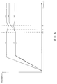
- FIG. 3 is a graph of voltage vs. time in the prior art power supply shown in FIG. 2 ;
- FIG. 4 is a block diagram of a power switch circuit according to a first embodiment of the present invention.
- FIG. 5 is a block diagram of a power supply according to the first embodiment of the present invention.
- FIG. 6 is a graph of voltage vs. time in the power supply shown in FIG. 5 when a voltage difference between the two power sources 20 , 21 is relative less;
- FIG. 7 is a graph of voltage vs. time in the power supply shown in FIG. 5 when a voltage difference between the two power sources 20 , 21 is relative larger;
- FIG. 8 is a block diagram of a power supply according to a second embodiment of the present invention.
- FIG. 9 is a block diagram of a power switch circuit according to the second embodiment of the present invention.
- FIG. 10 is a block diagram of a power switch circuit according to a third embodiment of the present invention.
- FIG. 11 is a block diagram of a power supply according to the third embodiment of the present invention.
- the power switch circuit 1 which generally includes a voltage input terminal Vin, a voltage output terminal Vout, a power transistor 10 , a control logic 11 , a first reverse current monitoring circuit 12 , and a second reverse current monitoring circuit 13 .
- the voltage input terminal Vin is provided to be coupled to a power source (not shown).
- the power source may have a voltage, for example, in a range of 5 ⁇ 20V.
- a power source that is compliant to a USB power delivery supplies a voltage of 5V, 12V or 20V.
- the voltage output terminal Vout is provided to be coupled to a load (not shown).
- the load may be an electronic component or device, such as, a capacitor, an inductor, a resistor, a cell phone, a USB flash drive or a USB portable hard drive.
- the power transistor 10 is operatively connected between the voltage input terminal Vin and the voltage output terminal Vout. More specifically, the power transistor 10 has two connecting terminals D, S and a control terminal G. The two connecting terminals D, S are respectively coupled to the voltage input terminal Vin and the voltage output terminal Vout.
- the control logic 11 is coupled to the control terminal G of the power transistor 10 for controlling the operation of the power transistor 10 so as to have the power source supply power to the load via the power transistor 10 .
- the power transistor 10 may be a n-type or p-type MOSFET (NMOS or PMOS), a bipolar junction transistor (BJT) or an insulated gate bipolar transistor (IGBT), etc.
- the power transistor 10 is a NMOS with two connecting terminals, namely Source and Drain, and a control terminal, namely Gate.
- the two connecting terminals D, S of the power transistor 10 are respectively coupled to the voltage input terminal Vin and the voltage output terminal Vout while the control terminal G of the power transistor 10 is coupled to an output of the control logic 11 .
- the control logic 11 is a charge pump, yet it is recognized that other types of control circuit may be employed to carry out the invention. For instance, if the power transistor 10 is a PMOS, the control logic 11 may be a soft-start circuit in lieu of the charge pump.
- control logic 11 provides a control signal to the control terminal G of the power transistor 10 so as to control the operation of the power transistor 10 , and therefore control the power transfer from the power source to the load. Moreover, the control logic 11 may adjust a duty cycle of the control signal according to the output voltage on the voltage output terminal Vout or the current flowing through the power transistor 10 .
- the first reverse current monitoring circuit 12 is coupled to the power transistor 10 and is configured to detect whether there exists a reverse current Ir that is large enough and flows through the power transistor 10 to the voltage input terminal Vin for a predetermined period of time. If yes, the first reverse current monitoring circuit 10 will turn off the power transistor 10 to stop the reverse current Ir from further flowing in the voltage input terminal Vin, thereby protecting the interior electronic components of the power source from being damaged.
- the first reverse current monitoring circuit 12 includes a first comparator 120 (OP 1 ) and a time-delay circuit 121 .
- the first comparator 120 has a first input coupled to receive a first voltage on the voltage output terminal Vout, a second input coupled to receive a second voltage on the voltage input terminal Vin, and a single-ended output coupled to an input of the time-delay circuit 121 .
- the first comparator 120 compares the first voltage to the second voltage, and sends a reverse current indicator via the output to the time-delay circuit 121 only when a voltage difference between the first and second voltages is larger than a first predetermined voltage value and therefore is identified by the first comparator 120 .
- the time-delay circuit 121 has an output coupled to the control terminal G of the power transistor 10 .
- a voltage difference between the first and second voltages is larger than a first predetermined voltage value, such as one in the range of 20 mV to 100 mV, it means that the reverse current Ir is sufficiently large to be detected or identified.
- the first comparator 120 sends out the reverse current indicator to the time-delay circuit 121 .
- the time-delay circuit 121 starts counting how long the reverse current indicator continues.
- the time-delay circuit 121 sends a shutdown signal to the control terminal G of the power transistor 10 to turn off the power transistor 10 , thereby stopping the reverse current Ir from flowing in the voltage input terminal Vin, and protecting the related electronic components of the power source from being damaged.
- the power transistor 10 is turned off, not immediately, but rather in a later time (after the predetermined period of time) by the time-delay circuit 121 . This avoids any misjudgment of the reverse current Ir.
- the reverse current Ir may merely be a noise or a transient current caused by any other reasons. In that case, there is no need to stop that current.
- the time-delay circuit 121 will not send the shutdown signal, and the power transistor 10 remains in the normal operation.
- the reverse current Ir is so small that the voltage difference between the voltage input terminal Vin and the voltage output terminal Vout is less than a first predetermined voltage value, such as 20 mV, which the first comparator 120 can notice or identify, then no reverse current indicator will be send out from the output of the first comparator 120 , and therefore no reverse current indicator will be received by the time-delay circuit 121 .
- the time-delay circuit 121 will not send out the shutdown signal to have the power transistor 10 turned off, and the extremely small reverse current Jr can still flow through the power transistor 10 to the voltage input terminal Vin. Fortunately, the reverse current Ir is too small to damage the electronic components of the power source coupled to the voltage input terminal Vin.
- the reverse current Ir is so large that the voltage difference between the voltage input terminal Vin and the voltage output terminal Vout is larger than a voltage value, such as 100 mV, the reverse current Ir may be too large that it can immediately damage the electronic components of the power source coupled to the voltage input terminal Vin. Thus, no matter it is a noise or any transient current caused by any other reasons, the power transistor 10 will be immediately turned off by the second reverse current monitoring circuit to protect the electronic components of the power source from damage of the reverse current Ir.
- the second reverse current monitoring circuit 13 is coupled to the power transistor 10 and is configured to detect whether a reverse current that is sufficiently large and flows through the power transistor 10 to the voltage input terminal Vin. If yes, the second reverse current monitoring circuit 13 will immediately turn off the power transistor 10 to stop the reverse current Ir. In particular, the second reverse current monitoring circuit 13 detects a larger reverse current Ir than does the first reverse current monitoring circuit 12 .
- the second reverse current monitoring circuit 13 includes a second comparator 130 (OP 2 ) that has a first input coupled to receive a first voltage on the voltage output terminal Vout, a second input coupled to receive a second voltage on the voltage input terminal Vin, and a single-ended output coupled to the control terminal G of the power transistor 10 .
- the second comparator 130 compares the first voltage to the second voltage, and outputs an OFF signal via its output to the control terminal G of the power transistor 10 to turn off the power transistor 10 only when a voltage difference between the first and second voltages is larger than a second predetermined voltage value and therefore is identified by the second comparator 130 .
- the second predetermined voltage value which can be noticed or identified by the second comparator 130 of the second reverse current monitoring circuit 13 is larger than the first predetermined voltage value which can be noticed or identified by the first comparator 120 of the first reverse current monitoring circuit 12 .
- the second comparator 130 detects a higher voltage difference, such as more than 100 mV, than does the first comparator 120 .
- the second reverse current monitoring circuit 13 will send out an OFF signal from the output of the second comparator 130 in order to immediately turn off the power transistor 10 , thereby blocking the extremely large reverse current Ir.
- the power switch circuit 1 can not only block the reverse current Ir from flowing to the power source which is coupled to the voltage input terminal Vin for protection of the interior electronic components, but also avoid malfunction caused by a noise or any transient current.
- FIG. 5 illustrates a block diagram of a power circuit 100 according to a first embodiment of the invention.
- the power circuit 100 includes two power switch circuits 1 , each of which is as recited above, to provide control the power transfer from the two power sources 20 , 21 to the load 3 .
- the first voltage input terminal Vin 1 of the first, left-side power switch circuit 1 is coupled to the first power source 20 while the second voltage input terminal Vin 2 of the second, right-side power switch circuit 1 is coupled to the second power source 21 .
- the voltage output terminals Vout of the two power switch circuits 1 are joined together and coupled to the load 3 .
- the two power source 20 , 21 may provide voltages in the range of about 5V to 20V, for example. And the voltages that the two power source 20 , 21 provide may be identical or not as required.
- the first and second power sources 20 , 21 may supply different voltages, for example 5V and 6V respectively.
- the two control logics 11 such as charge pumps, are in control.
- the first power transistor 10 (M 1 ) is in the ON-state while the second power transistor 10 (M 2 ) is in the OFF-state.
- the first power source 20 which is connected to the first voltage input terminal Vin 1 , supplies power through the power transistor 10 (M 1 ) to the load 3 .
- the output voltage magnitude Vo on the voltage output terminal Vout is slightly less than or equal to the input voltage magnitude V 1 on the first voltage input terminal Vin 1 .
- the second power source 21 starts to supply power through the second power transistor 10 (M 2 ) to the load 3 .
- the current may flow from the second power source 21 through the second voltage input terminal Vin 2 , the second power transistor 10 (M 2 ), the voltage output terminal Vout, the first power transistor 10 (M 1 ), the first voltage input terminal Vin 1 , and finally to the first power source 20 .
- the input voltage magnitude V 1 on the first voltage input tell final Vin 1 rises, as depicted in FIG. 6 .
- the output voltage magnitude Vo on the voltage output terminal Vout also rises due to the powering of the second power source 21 .
- the input voltage magnitude V 2 on the second voltage input terminal Vin 2 drops because a portion of the current coming from the second power source 21 goes to the first power source 20 .
- the voltage difference between output voltage magnitude Vo and the input voltage magnitude V 1 is larger than the first predetermined voltage value, such as 20 mV. That is, the voltage difference is sufficiently large to be identified by the first comparator 120 (OP 1 ), and therefore the first comparator 120 sends a reverse current indicator via its output to the time-delay circuit 121 .
- the time-delay circuit 121 starts to count for a predetermined period of time, such as 5 ms, which ends at time T 3 . It is understood that, if the first comparator 120 (M 1 ), at time T 3 , remains sending the reverse current indicator, it is deemed that the current flowing through the first power transistor 10 (M 1 ) to the voltage input terminal Vin is indeed the reverse current Ir, which is supposed to be blocked, and is not a noise or any other transient current. Accordingly, the time-delay circuit 121 will immediately send out a shutdown signal to the first power transistor 10 (M 1 ) at time T 3 to turn off the first power transistor 10 (M 1 ) and stop the reverse current Ir from further flowing to the voltage input terminal Vin.
- a predetermined period of time such as 5 ms
- the input voltage magnitude V 1 on the first voltage input terminal Vin 1 drops back to its original value.
- the input voltage magnitude V 2 on the second voltage input terminal Vin 2 rises back to its original value because the second power source 21 is no longer supplying power to the first voltage input terminal Vin 1 .
- the output voltage magnitude Vo continues to rise and finally be slightly less or equal to the input voltage magnitude V 2 on the second voltage input terminal Vin 2 because the second power source 21 coupled to the second voltage input terminal Vin 2 keeps supplying power through the second power transistor 10 (M 2 ) to the load 3 .
- the voltage difference between the first and second power sources 20 , 21 is not sufficiently large (or the reverse current Ir is not sufficiently large)
- the voltage difference between the output voltage magnitude Vo and the input voltage magnitude V 1 at time T 3 is less than a minimum voltage, such as 101 mV, which the second comparator 130 (OP 2 ) can detect or perceive.
- the second comparator 130 (OP 2 ) will not send any signals for turning off the power transistor 10 (M 1 ). Accordingly, the OFF-state of the power transistor 10 (M 1 ) is actually caused by the first reverse current monitoring circuit 12 , rather than the second reverse current monitoring circuit 13 .
- the first and second power sources 20 , 21 supply different voltages, for example 5V and 7V respectively, and the voltage difference between the first and second power sources 20 , 21 is now larger than that shown in FIG. 6 .
- the two control logics 11 are still in control.
- the first power transistor 10 (M 1 ) is in the ON-state while the second power transistor 10 (M 2 ) is in the OFF-state.
- the first power source 20 supplies power through the power transistor 10 (M 1 ) to the load 3 .
- the output voltage magnitude Vo on the voltage output terminal Vout is slightly less than or equal to the input voltage magnitude V 1 on the first voltage input terminal Vin 1 .
- the second power source 21 starts to supply power through the second power transistor 10 (M 2 ) to the load 3 .
- the current may flow from the second power source 21 through the second voltage input terminal Vin 2 , the second power transistor 10 (M 2 ), the voltage output terminal Vout, the first power transistor 10 (M 1 ), the first voltage input terminal Vin 1 , and finally to the first power source 20 .
- the input voltage magnitude V 1 on the first voltage input terminal Vin 1 rises, as depicted in FIG. 7 .
- the output voltage magnitude Vo on the voltage output terminal Vout also rises due to the powering of the second power source 21 .
- the input voltage magnitude V 2 on the second voltage input terminal Vin 2 drops because the second power source 21 may supply power to the first voltage input terminal Vin 1 .
- the voltage difference between the first and second power sources 20 , 21 is now larger than that shown in FIG. 6 .
- the voltage difference between output voltage magnitude Vo and the input voltage magnitude V 1 is larger than the first predetermined voltage value, such as 20 mV, and therefore can be detected or identified by the first comparator 120 (OP 1 ).
- the first comparator 120 (OP 1 ) sends a reverse current indicator via its output to the time-delay circuit 121 .
- the time-delay circuit 121 starts to count for a predetermined period of time, such as 5 ms, which will end at time T 3 ′′.
- the voltage difference between output voltage magnitude Vo and the input voltage magnitude V 1 is too large to be identified by the first comparator 120 (OP 1 ), but is larger than the second predetermined voltage value, such as 100 mV, and therefore can be detected or identified by the second comparator 130 (OP 2 ).
- the reverse current Ir at time T 3 ′ is too large that it may immediately damage the electronic components of the power source 20 .
- the second comparator 130 (OP 2 ) will immediately send an OFF signal via its output to the control terminal G of the power transistor 10 to turn off the power transistor 10 , thereby blocking the extremely large reverse current Ir and protecting the electronic components of the power source 20 from damage.
- the input voltage magnitude V 1 on the first voltage input terminal Vin 1 will drop back to its original value.
- the output voltage magnitude Vo continues to rise and finally be slightly less or equal to the input voltage magnitude V 2 on the second voltage input terminal Vin 2 because the second power source 21 keeps supplying power through the second power transistor 10 (M 2 ) to the load 3 .
- the input voltage magnitude V 2 on the second voltage input terminal Vin 2 will rise back to its original value because the second power source 21 is no longer supplying power to the first voltage input terminal Vin 1 .
- the time-delay circuit 121 may send out a shutdown signal to the power transistor 10 (M 1 ) as the counting is complete; however, earlier than that, the power transistor 10 (M 1 ) has already been turned off by the second comparator 130 (OP 2 ). Consequently, in the case where the voltage difference between the first and second power sources 20 , 21 is larger than that shown in FIG. 6 , the OFF-state of the power transistor 10 (M 1 ) is in fact caused by the second reverse current monitoring circuit 13 , rather than the first reverse current monitoring circuit 12 .
- the first and second power switch circuits 1 in the power circuit 100 are identical to each other. Thus, it is understood that if the input voltage magnitude V 1 on the first voltage input terminal Vin 1 is replaced by 6 V or 7 V, and the input voltage magnitude V 2 on the second voltage input terminal Vin 2 is replaced by 5 V, then the power circuit 100 will perform the same operation as described above, except that the reverse current Ir may occur and flow through the power transistor 10 (M 2 ) to the second voltage input terminal V 2 , and will be blocked by the first and second comparators 12 , 13 of the second, right-side power switch circuit 1 .
- FIG. 8 illustrates a block diagram of a power circuit 101 according to a second embodiment of the invention.
- the power circuit 101 includes a first power switch circuit 1 as recited above and a second power switch circuit 1 a to control power transfer from the two power sources 20 , 21 to the load 3 .
- the power circuit 101 operates in a similar way to the power circuit 100 , except that the second power switch 1 a employs a control logic 11 a to control a power transistor 10 a (M 2 ) without the first and second reverse current monitoring circuits 12 , 13 for reverse current control.
- the control logic 11 may be a charge pump or other control circuits, as mentioned above. Since there is no reverse current blocking mechanism in the second power switch circuit 1 a , the power circuit 101 can perform a reverse current blocking function with the first power switch 1 only when the voltage of the second power source 21 is larger than that of the first power source 20 .
- FIG. 9 there is shown a second embodiment of the power switch circuit 4 , which generally includes a voltage input terminal Vin, a voltage output terminal Vout, a power transistor 40 , a control logic 41 , a first reverse current monitoring circuit 43 , and a second reverse current monitoring circuit 44 .
- the voltage input terminal Vin, the voltage output terminal Vout, the power transistor 40 , and the control logic 41 are substantially identical to the voltage input terminal Vin, the voltage output terminal Vout, the power transistor 10 , and the control logic 11 shown in FIG. 4 respectively, and accordingly, is not further detailed herein.
- the first reverse current monitoring circuit 43 includes a current detecting circuit 430 , a first current sensing circuit 431 , and a time-delay circuit 432 .
- the current detection circuit 430 is coupled to the power transistor 40 for detecting a current flowing through the power transistor 40 .
- the current detection circuit 430 includes a reference current source (Iref) and a power transistor M.
- the power transistor M and the power transistor 40 are identical to each other and together form a current mirror circuit. In this manner, the current detection circuit 430 can obtain the current flowing through the power transistor 40 .
- the first current sensing circuit 431 has an input coupled to the current detection circuit 430 and an output coupled to an input of the time-delay circuit 432 . Only when the current flowing through the power transistor 40 to the voltage input terminal Vin is detected by the current detection circuit 430 and is larger than a first preset current value, the first current sensing circuit 431 sends a reverse current indicator to the time-delay circuit 432 , indicating that a reverse current Ir is flowing through the power transistor 40 to the voltage input terminal Vin.
- the time-delay circuit 432 has an output coupled to a control terminal G of the power transistor 40 , and only when the first current sensing circuit 431 persists outputting the reverse current indicator for a predetermined period of time, the time-delay circuit 432 sends a shutdown signal to the control terminal G of the power transistor 40 to turn off the power transistor 40 . As explained above, this can stop the reverse current Ir from further flowing to the voltage input terminal Vin, protect the interior electronic components of the power source from damage, and avoid the misjudgment.
- the second reverse current monitoring circuit 44 includes only a second current sensing circuit 441 that has an input coupled to the current detection circuit 430 , and an output coupled to the control terminal G of the power transistor 40 . Moreover, the second current sensing circuit 44 will send an OFF signal to the control terminal G of the power transistor 40 to turn off the power transistor 40 only when the current flowing through the power transistor 40 to the voltage input terminal Vin is detected by the current detection circuit 430 and is larger than a second preset current value.
- the second preset current value which can be identified by the second current sensing circuit 441 of the second reverse current monitoring circuit 44 is larger than the first preset current value which can be identified by the first current sensing circuit 431 of the first reverse current monitoring circuit 43 .
- the second reverse current monitoring circuit 44 can drive the power transistor 40 to block a relatively larger reverse current Ir.
- the power switch circuit 4 may be applied to the aforementioned power circuit 100 or 101 to replace the power switch circuit 1 .
- the power switch circuit 5 which generally includes a circuit 1 (framed by a dotted line) and an overvoltage protection circuit 50 .
- the circuit 1 is identical to the power switch circuit 1 as recited above, and accordingly, is not further detailed herein.
- the power switch circuit 5 further includes the overvoltage protection circuit 50 which is operatively connected between the voltage input terminal Vin and a control terminal G of the power transistor 10 .
- the overvoltage protection circuit 50 is configured to turn off the power transistor 10 only when an input voltage magnitude on the voltage input terminal Vin is detected to be larger than a preset upper limit of voltage value, such as 100 mV or more.
- the reverse current Ir flowing to the voltage input terminal Vin may still cause the input voltage magnitude V 1 on the voltage input terminal Vin to rise gradually.
- the overvoltage protection circuit 50 can detect when the input voltage magnitude V 1 on the voltage input terminal Vin exceeds the preset upper limit of voltage value, and send an OFF signal to the control terminal G of the power transistor 10 to have the power transistor 10 turned off, thereby blocking the reverse current Ir from flowing into the voltage input terminal Vin, and preventing the input voltage magnitude V 1 on the voltage input terminal Vin from reaching a voltage value that can damage the electronic components of the power source coupled to the voltage input terminal Vin.
- overvoltage protection circuit 50 may be applied to the aforementioned power switch circuit 4 to provide the overvoltage protection function.
- FIG. 11 illustrates a block diagram of a power circuit 102 according to a third embodiment of the invention.
- the power circuit 102 includes two power switch circuits 5 as recited above to control power transfer from two power sources (not shown) to a load 3 .
- the power circuit 102 blocks not only the larger reverse current Ir which can be detected by the first or second reverse current monitoring circuit 12 or 13 , but also the extremely small reverse current Ir, which has lasted for a long time, before the extremely small reverse current Ir becomes a disaster to the electronic components of the power source.
Landscapes
- Engineering & Computer Science (AREA)
- Power Engineering (AREA)
- Theoretical Computer Science (AREA)
- Physics & Mathematics (AREA)
- General Engineering & Computer Science (AREA)
- General Physics & Mathematics (AREA)
- Direct Current Feeding And Distribution (AREA)
- Electronic Switches (AREA)
- Power Conversion In General (AREA)
Abstract
Description
Claims (15)
Applications Claiming Priority (3)
| Application Number | Priority Date | Filing Date | Title |
|---|---|---|---|
| CN201610357252.9 | 2016-05-26 | ||
| CN201610357252.9A CN107437888B (en) | 2016-05-26 | 2016-05-26 | Power switch circuit and applied power supply circuit |
| CN201610357252 | 2016-05-26 |
Publications (2)
| Publication Number | Publication Date |
|---|---|
| US20170346284A1 US20170346284A1 (en) | 2017-11-30 |
| US10637237B2 true US10637237B2 (en) | 2020-04-28 |
Family
ID=60418372
Family Applications (1)
| Application Number | Title | Priority Date | Filing Date |
|---|---|---|---|
| US15/448,234 Expired - Fee Related US10637237B2 (en) | 2016-05-26 | 2017-03-02 | Power switch circuit and power circuit with the same |
Country Status (3)
| Country | Link |
|---|---|
| US (1) | US10637237B2 (en) |
| CN (1) | CN107437888B (en) |
| TW (1) | TWI618341B (en) |
Families Citing this family (9)
| Publication number | Priority date | Publication date | Assignee | Title |
|---|---|---|---|---|
| KR102757507B1 (en) * | 2017-02-13 | 2025-01-20 | 삼성전자주식회사 | Reverse voltage monitoring circuit capable of reducing power consumption and Semiconductor device having the same |
| EP3477837B1 (en) * | 2017-10-25 | 2025-07-16 | Sciosense B.V. | Charge pump structure with regulated output voltage |
| US10969809B2 (en) * | 2018-08-02 | 2021-04-06 | Microchip Technology Incorporated | Dual input LDO voltage regulator |
| CN109613326A (en) * | 2018-12-18 | 2019-04-12 | 上海南芯半导体科技有限公司 | A kind of input over-voltage detection circuit that can work independently and its implementation |
| CN109494990B (en) * | 2019-01-03 | 2020-11-06 | 深圳市基准半导体有限公司 | Load transient response speed improving method based on variable frequency and transconductance |
| CN115427918B (en) * | 2020-05-01 | 2025-11-25 | 高通股份有限公司 | Power supply circuit with reduced leakage current |
| TWI722900B (en) * | 2020-05-14 | 2021-03-21 | 絡達科技股份有限公司 | Power switch control circuit |
| JP2023037688A (en) * | 2021-09-06 | 2023-03-16 | キヤノン株式会社 | Information processing apparatus, method for controlling information processing apparatus, and program |
| TWI828497B (en) * | 2022-12-29 | 2024-01-01 | 香港商香港德潤微電子股份有限公司 | Reverse current protection circuit |
Citations (13)
| Publication number | Priority date | Publication date | Assignee | Title |
|---|---|---|---|---|
| US4731574A (en) * | 1983-11-15 | 1988-03-15 | Sgs-Ates Deutschland Halbleiter Bauelemente Gmbh | Series voltage regulator with limited current consumption at low input voltages |
| US5375029A (en) | 1992-10-09 | 1994-12-20 | Mitsubishi Denki Kabushiki Kaisha | Overcurrent protection circuit of power device and semiconductor integrated circuit device |
| US20020130645A1 (en) * | 2001-03-15 | 2002-09-19 | Sheng-Nan Tsai | Overvoltage protection device for buck converter |
| TWI229500B (en) | 2004-02-02 | 2005-03-11 | Aimtron Technology Corp | Soft-start charge pump circuit |
| US20060208773A1 (en) | 2005-03-14 | 2006-09-21 | Infineon Technologies Ag | Circuit arrangement with a transistor having a reduced reverse current |
| US20080285191A1 (en) * | 2005-12-09 | 2008-11-20 | Ricoh Company, Ltd. | Backflow preventing circuit capable of preventing reverse current efficiently |
| TWI335704B (en) | 2005-09-21 | 2011-01-01 | Richtek Technology Corp | |
| US20110085274A1 (en) * | 2008-07-05 | 2011-04-14 | Qinetiq Limited | Circuit breaker |
| TWI355801B (en) | 2008-04-01 | 2012-01-01 | Richtek Technology Corp | Dual power switch and voltage regulator using same |
| TWI369057B (en) | 2009-03-13 | 2012-07-21 | Advanced Analog Technology Inc | Boost converter having two-step soft start mechanism |
| TWI369828B (en) | 2008-03-12 | 2012-08-01 | O2Micro Int Ltd | Monitoring and control circuit, protecting circuit and the method for adjusting current thereof |
| CN103166442A (en) | 2013-03-27 | 2013-06-19 | 华为技术有限公司 | Device for preventing current of buck circuit from flowing reversely, converter and power supply |
| CN203747365U (en) | 2013-12-26 | 2014-07-30 | 上海新进半导体制造有限公司 | USB circuit |
-
2016
- 2016-05-26 CN CN201610357252.9A patent/CN107437888B/en not_active Expired - Fee Related
- 2016-09-01 TW TW105128296A patent/TWI618341B/en not_active IP Right Cessation
-
2017
- 2017-03-02 US US15/448,234 patent/US10637237B2/en not_active Expired - Fee Related
Patent Citations (14)
| Publication number | Priority date | Publication date | Assignee | Title |
|---|---|---|---|---|
| US4731574A (en) * | 1983-11-15 | 1988-03-15 | Sgs-Ates Deutschland Halbleiter Bauelemente Gmbh | Series voltage regulator with limited current consumption at low input voltages |
| US5375029A (en) | 1992-10-09 | 1994-12-20 | Mitsubishi Denki Kabushiki Kaisha | Overcurrent protection circuit of power device and semiconductor integrated circuit device |
| US20020130645A1 (en) * | 2001-03-15 | 2002-09-19 | Sheng-Nan Tsai | Overvoltage protection device for buck converter |
| TWI229500B (en) | 2004-02-02 | 2005-03-11 | Aimtron Technology Corp | Soft-start charge pump circuit |
| US20060208773A1 (en) | 2005-03-14 | 2006-09-21 | Infineon Technologies Ag | Circuit arrangement with a transistor having a reduced reverse current |
| TWI335704B (en) | 2005-09-21 | 2011-01-01 | Richtek Technology Corp | |
| US20080285191A1 (en) * | 2005-12-09 | 2008-11-20 | Ricoh Company, Ltd. | Backflow preventing circuit capable of preventing reverse current efficiently |
| TWI369828B (en) | 2008-03-12 | 2012-08-01 | O2Micro Int Ltd | Monitoring and control circuit, protecting circuit and the method for adjusting current thereof |
| TWI355801B (en) | 2008-04-01 | 2012-01-01 | Richtek Technology Corp | Dual power switch and voltage regulator using same |
| US20110085274A1 (en) * | 2008-07-05 | 2011-04-14 | Qinetiq Limited | Circuit breaker |
| TWI369057B (en) | 2009-03-13 | 2012-07-21 | Advanced Analog Technology Inc | Boost converter having two-step soft start mechanism |
| CN103166442A (en) | 2013-03-27 | 2013-06-19 | 华为技术有限公司 | Device for preventing current of buck circuit from flowing reversely, converter and power supply |
| CN103166442B (en) | 2013-03-27 | 2016-05-25 | 华为技术有限公司 | Prevent device, converter and power supply that step-down buck circuital current is reverse |
| CN203747365U (en) | 2013-12-26 | 2014-07-30 | 上海新进半导体制造有限公司 | USB circuit |
Also Published As
| Publication number | Publication date |
|---|---|
| US20170346284A1 (en) | 2017-11-30 |
| CN107437888A (en) | 2017-12-05 |
| CN107437888B (en) | 2019-11-01 |
| TWI618341B (en) | 2018-03-11 |
| TW201742357A (en) | 2017-12-01 |
Similar Documents
| Publication | Publication Date | Title |
|---|---|---|
| US10637237B2 (en) | Power switch circuit and power circuit with the same | |
| CN106848998B (en) | A kind of power output protection circuit and device | |
| US10778019B2 (en) | Reverse current prevention for FET used as reverse polarity protection device | |
| TWI610528B (en) | Boost-type switching regulator and electronic device | |
| JP5708817B2 (en) | Load drive circuit | |
| US20150207307A1 (en) | Boost apparatus with over-current and over-voltage protection function | |
| US9825454B2 (en) | Protection device and method for electronic device | |
| US20140111899A1 (en) | Protecting circuit | |
| US20140239884A1 (en) | Charge and discharge control circuit and battery device | |
| JP5610484B2 (en) | Power supply reverse connection protection circuit | |
| US10256805B2 (en) | Protective circuit with current regulating digital output module | |
| US9444447B2 (en) | Load drive circuit | |
| US20120092800A1 (en) | Circuit for detecting over-voltage and over-current | |
| US20110127984A1 (en) | Linear voltage regulator circuit with power saving capability | |
| US8570018B2 (en) | Hot swappable synchronous buck regulator | |
| WO2018069123A1 (en) | A circuit protection arrangement | |
| US9766299B2 (en) | Method for electronically testing integrity of ideal diode components used in OR'd voltage bus | |
| US10605869B2 (en) | Battery voltage detector | |
| US9684323B2 (en) | Regulator circuit that suppresses an overshoot of output voltage | |
| US9966834B2 (en) | Power supply protecting apparatus | |
| US10910830B2 (en) | Electrical protective circuit | |
| JP6519498B2 (en) | Switching power supply | |
| CN105515363A (en) | Power supply circuit and its soft start circuit | |
| US9257898B1 (en) | Power supplying circuit and soft-start circuit of the same | |
| US9941686B2 (en) | Sensor device |
Legal Events
| Date | Code | Title | Description |
|---|---|---|---|
| AS | Assignment |
Owner name: GREEN SOLUTION TECHNOLOGY CO., LTD., TAIWAN Free format text: ASSIGNMENT OF ASSIGNORS INTEREST;ASSIGNORS:LEE, LI-MIN;LIU, ZHONG-WEI;SHIU, SHIAN-SUNG;AND OTHERS;SIGNING DATES FROM 20160711 TO 20160714;REEL/FRAME:041460/0563 |
|
| STPP | Information on status: patent application and granting procedure in general |
Free format text: DOCKETED NEW CASE - READY FOR EXAMINATION |
|
| STPP | Information on status: patent application and granting procedure in general |
Free format text: NON FINAL ACTION MAILED |
|
| STPP | Information on status: patent application and granting procedure in general |
Free format text: RESPONSE TO NON-FINAL OFFICE ACTION ENTERED AND FORWARDED TO EXAMINER |
|
| STPP | Information on status: patent application and granting procedure in general |
Free format text: FINAL REJECTION MAILED |
|
| STPP | Information on status: patent application and granting procedure in general |
Free format text: NOTICE OF ALLOWANCE MAILED -- APPLICATION RECEIVED IN OFFICE OF PUBLICATIONS |
|
| STCF | Information on status: patent grant |
Free format text: PATENTED CASE |
|
| FEPP | Fee payment procedure |
Free format text: MAINTENANCE FEE REMINDER MAILED (ORIGINAL EVENT CODE: REM.); ENTITY STATUS OF PATENT OWNER: SMALL ENTITY |
|
| LAPS | Lapse for failure to pay maintenance fees |
Free format text: PATENT EXPIRED FOR FAILURE TO PAY MAINTENANCE FEES (ORIGINAL EVENT CODE: EXP.); ENTITY STATUS OF PATENT OWNER: SMALL ENTITY |
|
| STCH | Information on status: patent discontinuation |
Free format text: PATENT EXPIRED DUE TO NONPAYMENT OF MAINTENANCE FEES UNDER 37 CFR 1.362 |
|
| FP | Lapsed due to failure to pay maintenance fee |
Effective date: 20240428 |