US10629523B2 - Via-based vertical capacitor and resistor structures - Google Patents
Via-based vertical capacitor and resistor structures Download PDFInfo
- Publication number
- US10629523B2 US10629523B2 US16/126,406 US201816126406A US10629523B2 US 10629523 B2 US10629523 B2 US 10629523B2 US 201816126406 A US201816126406 A US 201816126406A US 10629523 B2 US10629523 B2 US 10629523B2
- Authority
- US
- United States
- Prior art keywords
- electrically conductive
- conductive layers
- layers
- electrically
- substrate
- Prior art date
- Legal status (The legal status is an assumption and is not a legal conclusion. Google has not performed a legal analysis and makes no representation as to the accuracy of the status listed.)
- Expired - Fee Related
Links
Images


Classifications
-
- H—ELECTRICITY
- H10—SEMICONDUCTOR DEVICES; ELECTRIC SOLID-STATE DEVICES NOT OTHERWISE PROVIDED FOR
- H10W—GENERIC PACKAGES, INTERCONNECTIONS, CONNECTORS OR OTHER CONSTRUCTIONAL DETAILS OF DEVICES COVERED BY CLASS H10
- H10W20/00—Interconnections in chips, wafers or substrates
- H10W20/40—Interconnections external to wafers or substrates, e.g. back-end-of-line [BEOL] metallisations or vias connecting to gate electrodes
- H10W20/495—Capacitive arrangements or effects of, or between wiring layers
- H10W20/496—Capacitor integral with wiring layers
-
- H01L23/5223—
-
- H01L23/5226—
-
- H01L23/5228—
-
- H01L27/01—
-
- H—ELECTRICITY
- H10—SEMICONDUCTOR DEVICES; ELECTRIC SOLID-STATE DEVICES NOT OTHERWISE PROVIDED FOR
- H10D—INORGANIC ELECTRIC SEMICONDUCTOR DEVICES
- H10D86/00—Integrated devices formed in or on insulating or conducting substrates, e.g. formed in silicon-on-insulator [SOI] substrates or on stainless steel or glass substrates
- H10D86/80—Integrated devices formed in or on insulating or conducting substrates, e.g. formed in silicon-on-insulator [SOI] substrates or on stainless steel or glass substrates characterised by multiple passive components, e.g. resistors, capacitors or inductors
- H10D86/85—Integrated devices formed in or on insulating or conducting substrates, e.g. formed in silicon-on-insulator [SOI] substrates or on stainless steel or glass substrates characterised by multiple passive components, e.g. resistors, capacitors or inductors characterised by only passive components
-
- H—ELECTRICITY
- H10—SEMICONDUCTOR DEVICES; ELECTRIC SOLID-STATE DEVICES NOT OTHERWISE PROVIDED FOR
- H10W—GENERIC PACKAGES, INTERCONNECTIONS, CONNECTORS OR OTHER CONSTRUCTIONAL DETAILS OF DEVICES COVERED BY CLASS H10
- H10W20/00—Interconnections in chips, wafers or substrates
- H10W20/40—Interconnections external to wafers or substrates, e.g. back-end-of-line [BEOL] metallisations or vias connecting to gate electrodes
- H10W20/41—Interconnections external to wafers or substrates, e.g. back-end-of-line [BEOL] metallisations or vias connecting to gate electrodes characterised by their conductive parts
- H10W20/42—Vias, e.g. via plugs
-
- H—ELECTRICITY
- H10—SEMICONDUCTOR DEVICES; ELECTRIC SOLID-STATE DEVICES NOT OTHERWISE PROVIDED FOR
- H10W—GENERIC PACKAGES, INTERCONNECTIONS, CONNECTORS OR OTHER CONSTRUCTIONAL DETAILS OF DEVICES COVERED BY CLASS H10
- H10W20/00—Interconnections in chips, wafers or substrates
- H10W20/40—Interconnections external to wafers or substrates, e.g. back-end-of-line [BEOL] metallisations or vias connecting to gate electrodes
- H10W20/498—Resistive arrangements or effects of, or between, wiring layers
-
- H—ELECTRICITY
- H10—SEMICONDUCTOR DEVICES; ELECTRIC SOLID-STATE DEVICES NOT OTHERWISE PROVIDED FOR
- H10D—INORGANIC ELECTRIC SEMICONDUCTOR DEVICES
- H10D1/00—Resistors, capacitors or inductors
- H10D1/40—Resistors
- H10D1/47—Resistors having no potential barriers
-
- H—ELECTRICITY
- H10—SEMICONDUCTOR DEVICES; ELECTRIC SOLID-STATE DEVICES NOT OTHERWISE PROVIDED FOR
- H10D—INORGANIC ELECTRIC SEMICONDUCTOR DEVICES
- H10D1/00—Resistors, capacitors or inductors
- H10D1/60—Capacitors
- H10D1/68—Capacitors having no potential barriers
- H10D1/692—Electrodes
- H10D1/711—Electrodes having non-planar surfaces, e.g. formed by texturisation
- H10D1/714—Electrodes having non-planar surfaces, e.g. formed by texturisation having horizontal extensions
-
- H—ELECTRICITY
- H10—SEMICONDUCTOR DEVICES; ELECTRIC SOLID-STATE DEVICES NOT OTHERWISE PROVIDED FOR
- H10D—INORGANIC ELECTRIC SEMICONDUCTOR DEVICES
- H10D1/00—Resistors, capacitors or inductors
- H10D1/60—Capacitors
- H10D1/68—Capacitors having no potential barriers
- H10D1/692—Electrodes
- H10D1/711—Electrodes having non-planar surfaces, e.g. formed by texturisation
- H10D1/716—Electrodes having non-planar surfaces, e.g. formed by texturisation having vertical extensions
Definitions
- Certain aspects of the present disclosure generally relate to electronic circuits and, more particularly, to an integrated circuit that includes at least one of a vertical capacitor structure or a vertical resistor structure.
- ICs integrated circuits
- chips integrated circuits
- These integrated circuits are typically implemented as semiconductor dies packaged in integrated circuit packages.
- the semiconductor dies may include numerous active devices and/or passive devices located on-chip. These devices may occupy a large amount of area on the chip, reducing the amount of space available for other components.
- the integrated circuit generally includes a substrate oriented in a horizontal plane; a plurality of electrically conductive layers disposed above the substrate; a plurality of electrically insulative layers disposed above the substrate and interposed between the plurality of electrically conductive layers; and a vertical capacitor structure disposed in the plurality of electrically conductive layers and the plurality of electrically insulative layers.
- the vertical capacitor structure includes a first interconnection element disposed above the substrate; a second interconnection element disposed above the first interconnection element; one or more first fingers coupled to the first interconnection element and extending therefrom through a first set of the plurality of electrically conductive layers and through a first set of the plurality of electrically insulative layers, in a first vertical direction with respect to the horizontal plane of the substrate; and one or more second fingers coupled to the second interconnection element and extending therefrom through a second set of the plurality of electrically conductive layers and through a second set of the plurality of electrically insulative layers, in a second vertical direction with respect to the horizontal plane of the substrate.
- the first and second fingers have a capacitance therebetween.
- the integrated circuit includes a vertical resistor structure.
- the integrated circuit includes a substrate oriented in a horizontal plane; a plurality of electrically conductive layers disposed above the substrate; a plurality of electrically insulative layers disposed above the substrate and interposed between the plurality of electrically conductive layers; and a vertical resistor structure disposed in the plurality of electrically conductive layers and the plurality of electrically insulative layers.
- the vertical resistor structure includes a first set of interconnection elements disposed above the substrate; a second set of interconnection elements disposed above the first set of interconnection elements; and a plurality of fingers disposed between the first set of interconnection elements and the second set of interconnection elements.
- Each finger of the plurality of fingers extends vertically across the plurality of electrically conductive layers and the plurality of electrically insulative layers, with respect to the horizontal plane of the substrate. At least one of the plurality of fingers is coupled to one of the first set of interconnection elements and to one of the second set of interconnection elements.
- Certain aspects of the present disclosure provide a method for fabricating an integrated circuit with a vertical capacitor structure.
- the method generally includes forming a substrate oriented in a horizontal plane; forming a plurality of electrically conductive layers above the substrate; forming a plurality of electrically insulative layers above the substrate and interposed between the plurality of electrically conductive layers; and forming the vertical capacitor structure in the plurality of electrically conductive layers and the plurality of electrically insulative layers.
- Forming the vertical capacitor structure includes forming a first interconnection element above the substrate; forming a second interconnection element above the first interconnection element; forming one or more first fingers that couple to the first interconnection element and extend therefrom through a first set of the plurality of electrically conductive layers and through a first set of the plurality of electrically insulative layers, in a first vertical direction with respect to the horizontal plane of the substrate; and forming one or more second fingers that couple to the second interconnection element and extend therefrom through a second set of the plurality of electrically conductive layers and through a second set of the plurality of electrically insulative layers, in a second vertical direction with respect to the horizontal plane of the substrate.
- the first and second fingers have a capacitance therebetween.
- Certain aspects of the present disclosure provide a method for fabricating an integrated circuit with a vertical resistor structure.
- the method generally includes forming a substrate oriented in a horizontal plane; forming a plurality of electrically conductive layers above the substrate; forming a plurality of electrically insulative layers above the substrate and interposed between the plurality of electrically conductive layers; and forming the vertical resistor structure in the plurality of electrically conductive layers and the plurality of electrically insulative layers.
- Forming the vertical resistor structure includes forming a first set of interconnection elements above the substrate; forming a second set of interconnection elements above the first set of interconnection elements; and forming a plurality of fingers between the first set of interconnection elements and the second set of interconnection elements.
- Each finger of the plurality of fingers extends vertically across the plurality of electrically conductive layers and the plurality of electrically insulative layers, with respect to the horizontal plane of the substrate. At least one of the plurality of fingers is coupled to one of the first set of interconnection elements and to one of the second set of interconnection elements.
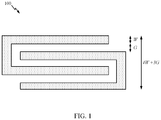
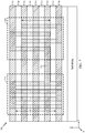
- FIG. 1 illustrates a top view of an example horizontal capacitive component.
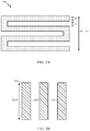
- FIG. 2A illustrates a top view of an example horizontal metallic resistive component.
- FIG. 2B illustrates a top view of example horizontal polysilicon resistive components.
- FIG. 3 illustrates a cross-sectional view of an integrated circuit that includes a via-based vertical capacitor structure, in accordance with certain aspects of the present disclosure.
- FIG. 4 illustrates a top view of the integrated circuit in FIG. 3 , in accordance with certain aspects of the present disclosure.
- FIG. 5 illustrates a cross-sectional view of an integrated circuit that includes a via-based vertical resistor structure, in accordance with certain aspects of the present disclosure.
- FIG. 6 illustrates a top view of the integrated circuit in FIG. 5 , in accordance with certain aspects of the present disclosure.
- FIG. 7 illustrates a cross-sectional view of an example integrated circuit that includes a via-based vertical resistor structure and a via-based vertical capacitor structure, in accordance with certain aspects of the present disclosure.
- FIG. 8 is a flow diagram of example operations for fabricating an integrated circuit that includes a via-based vertical capacitor structure, in accordance with certain aspects of the present disclosure.
- FIG. 9 is a flow diagram of example operations for fabricating an integrated circuit that includes a via-based vertical resistor structure, in accordance with certain aspects of the present disclosure.
- aspects of the present disclosure provide vertical capacitor structures and vertical resistor structures suitable for increasing the density of components located on an integrated circuit, for example. More specifically, aspects presented herein provide vertical capacitor structures and vertical resistor structures with reduced area footprints, reduced parasitic capacitance, and that allow for a process invariant resistor-capacitor (RC) time constant, compared to components within the integrated circuit that are oriented in parallel with a horizontal plane of the integrated circuit, for example.
- RC resistor-capacitor
- connection in the various tenses of the verb “connect” may mean that element A is directly connected to element B or that other elements may be connected between elements A and B (i.e., that element A is indirectly connected with element B).
- connection may also be used herein to mean that a wire, trace, or other electrically conductive material is used to electrically connect elements A and B (and any components electrically connected there between).
- passive components e.g., resistors, capacitors, etc. located on-chip are typically oriented horizontally (e.g., in parallel) with respect to the horizontal plane of the chip substrate (e.g., silicon (Si) substrate).
- the chip substrate e.g., silicon (Si) substrate.
- passive components that are oriented horizontally with respect to the chip substrate may occupy a significantly large area footprint on the chip.
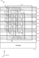
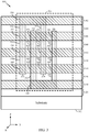
- FIG. 1 shows the top view of a capacitive component 100 (e.g., interdigitated metal capacitor), oriented horizontally with respect to the chip substrate, that occupies a large silicon area footprint.
- the capacitive component 100 may occupy a minimum width approximately equal to 4 W+3 G, where W is the width of a trace and G is the width of a gap (i.e., spacing) between traces.
- W is the width of a trace
- G is the width of a gap (i.e., spacing) between traces.
- W is equal to G
- the capacitive component 100 may occupy a minimum width approximately equal to 7 W.
- the width of each trace is the same (e.g., W)
- the widths of the traces within the capacitive component 100 may be different.
- FIG. 1 shows the top view of a capacitive component 100 (e.g., interdigitated metal capacitor), oriented horizontally with respect to the chip substrate, that occupies a large silicon area footprint.
- FIG. 2A shows the top view of a resistive component 200 (e.g., metal resistor), arranged in a plane parallel with the horizontally oriented chip substrate, that occupies a large silicon area footprint.
- FIG. 2B shows the top view of three resistive components 202 , 204 , and 206 (e.g., polysilicon resistors), oriented horizontally with respect to the chip substrate, that occupy a relatively large silicon area footprint.
- each resistive component 202 , 204 , and 206 may have a width determined based on
- R ⁇ ⁇ ⁇ L poly A poly , where R is the resistance of the resistive component, ⁇ is the resistivity of polysilicon in the resistive component, L poly is the length of polysilicon in the resistive component, and A poly is the cross-sectional area of polysilicon (e.g., through which current flows) in the resistive component.
- a poly W poly T poly , where W poly , is the width of the polysilicon in the resistive component, and T poly is the thickness of the polysilicon.
- the structure/orientation of passive components may reduce the efficiency and performance of the chip.
- capacitive component 100 as a reference example, the area footprint associated with capacitive component 100 may reduce the amount of available space located on the chip for other components, which in turn reduces area efficiency.
- the structure of capacitive component 100 can lead to increased parasitic capacitance, e.g., due to the amount of area (e.g., of the traces) in parallel and proximate to the chip substrate.
- integrated circuits that have both resistor and capacitor components located on chip may suffer from process-dependent RC time constant variation.
- process variations in attributes (e.g., length, width, thickness, etc.) of chip components can occur during fabrication of the integrated circuit.
- an integrated circuit includes a polysilicon resistor (e.g., resistive component 202 ) and interdigitated metal capacitor (e.g., capacitive component 100 )
- process variations may cause a RC time constant variation of up to ⁇ 30%.
- Certain aspects of the present disclosure provide structures for passive components (e.g., capacitors, resistors, etc.) that are oriented vertically with respect to a horizontal plane of a chip substrate.
- the structures described herein may be suitable, for example, for integrated circuit devices that include, but are not limited to, delay cells, clock trees, oscillators, decoupling capacitors, etc.
- the vertical capacitor structures and vertical resistor structures may include multiple (stacked) vias that extend vertically through multiple electrically conductive layers and multiple electrically insulative layers (of an integrated circuit) with respect to the horizontal plane of the chip substrate.
- aspects presented herein can reduce the amount of horizontal area occupied by such components on the substrate, reduce the parasitic capacitance of these components in an integrated circuit, and/or provide a process-invariant RC time constant.
- vertical direction or “vertical” generally refers to the z-direction
- horizontal direction or “horizontal” generally refers to directions in the x-y plane.
- FIG. 3 illustrates a cross-sectional view of an example integrated circuit (IC) 300 with a vertical capacitor structure 324 , in accordance with certain aspects of the present disclosure.
- the IC 300 includes a substrate 322 (e.g., Si substrate) with a horizontal orientation in the x-y plane; electrically conductive layers 302 , 306 , 310 , 314 , and 318 (collectively referred to as “electrically conductive layers of IC 300 ”) disposed above the substrate 322 ; and electrically insulative layers 304 , 308 , 312 , and 316 (collectively referred to as “electrically insulative layers of IC 300 ”) disposed above the substrate 322 .
- a substrate 322 e.g., Si substrate
- electrically conductive layers 302 , 306 , 310 , 314 , and 318 collectively conductive layers of IC 300
- electrically insulative layers 304 , 308 , 312 , and 316 collectively
- the IC 300 is depicted as having five electrically conductive layers, the reader is to understand that the IC 300 may include more or less than five electrically conductive layers. Similarly, while the IC 300 is depicted as having four electrically insulative layers, the reader is to understand that the IC 300 may include more or less than four electrically insulative layers.
- each electrically insulative layer 304 , 308 , 312 , and 316 may be disposed between a different pair of electrically conductive layers.
- electrically insulative layer 304 is disposed between electrically conductive layers 302 and 306 ;
- electrically insulative layer 308 is disposed between electrically conductive layers 306 and 310 ;
- electrically insulative layer 312 is disposed between electrically conductive layers 310 and 314 ;
- electrically insulative layer 316 is disposed between electrically conductive layers 314 and 318 .
- the electrically insulative layers may be interposed between the electrically conductive layers.
- the IC 300 may include a portion 320 disposed between the substrate 322 and the electrically conductive layer 318 .
- the portion 320 may include multiple layers (not shown in FIG. 3 ) of the same or different materials.
- the portion 320 may include a dielectric material as illustrated.
- Each of the electrically conductive layers of IC 300 may include a metal (e.g., copper (Cu), aluminum (Al), etc.), metal alloy, or silicon alloy.
- the electrically conductive layers of IC 300 may include the same material (e.g., metal, metal alloy, silicon alloy).
- at least one of the electrically conductive layers of IC 300 may include a different material than another one of the electrically conductive layers of IC 300 .
- Each of the electrically insulative layers of IC 300 may include a dielectric material (or a mixture of dielectric materials), such as aluminum oxide (Al 2 O 3 ), silicon dioxide (SiO 2 ), silicon nitride (Si 3 N 4 ), etc. While each of the electrically conductive layers of IC 300 and each of the electrically insulative layers of IC 300 are depicted as having approximately the same height/thickness, the reader is to understand that each of the electrically conductive layers of IC 300 and/or each of the electrically insulative layers of IC 300 can have a different height/thickness from other layers.
- a dielectric material such as aluminum oxide (Al 2 O 3 ), silicon dioxide (SiO 2 ), silicon nitride (Si 3 N 4 ), etc. While each of the electrically conductive layers of IC 300 and each of the electrically insulative layers of IC 300 are depicted as having approximately the same height/thickness, the reader is to understand that each of the electrically
- the vertical capacitor structure 324 is disposed in the electrically conductive layers of IC 300 and the electrically insulative layers of IC 300 . Although the vertical capacitor structure 324 is shown as occupying nearly all of the electrically conductive layers of IC 300 and the electrically insulative layers of IC 300 in the example of FIG. 3 , the vertical capacitor structure 324 need not utilize all or even the majority of the electrically conductive layers of IC 300 and the electrically insulative layers of IC 300 .
- the vertical capacitor structure 324 includes an interconnection element 340 disposed in the electrically conductive layer 318 above the substrate 322 , and an interconnection element 330 disposed in the electrically conductive layer 302 above the interconnection element 340 . Each of the interconnection elements 340 and 330 may include a metal, metal alloy, or silicon alloy, e.g., for an electrically conductive trace of the respective interconnection element.
- Each of the interconnection elements 340 and 330 is coupled to one or more fingers.
- the interconnection element 340 is coupled to fingers 342 and 344 , each of which extends from the interconnection element 340 through the electrically insulative layers 316 , 312 , and 308 , and the electrically conductive layers 314 , 310 , and 306 , in a vertical direction (e.g., positive z direction) towards the interconnection element 330 (e.g., with respect to the substrate 322 oriented in the x-y plane).
- the interconnection element 330 is coupled to fingers 332 and 334 , each of which extends from the interconnection element 330 through the electrically insulative layers 304 , 308 , and 312 , and the electrically conductive layers 306 , 310 , and 314 , in a vertical direction (e.g., negative z direction) towards the interconnection element 340 (e.g., with respect to the substrate 322 oriented in the x-y plane). Due to the dielectric properties of the insulative layers, a capacitance exists between the fingers 332 , 334 of the interconnection element 330 and the fingers 342 , 344 of the interconnection element 340 .
- Finger 342 is interposed laterally between fingers 332 and 334
- finger 334 is interposed laterally between fingers 342 and 344 .
- FIG. 3 depicts each of the interconnection elements 330 and 340 being coupled to two fingers, the reader is to understand that the interconnection elements 330 and 340 may be coupled to more or less than two fingers.
- the fingers 332 , 334 , 342 , and 344 may include one or more vias that extend through different sets of the electrically conductive layers of IC 300 and the electrically insulative layers of IC 300 .
- finger 332 includes (stacked) vias 350 , 352 , 354 , 356 , 358 , and 360 that extend (from interconnection element 330 ) through the electrically insulative layers 304 , 308 , and 312 and through the electrically conductive layers 306 , 310 , and 314 in a vertical direction (e.g., negative z direction) towards the interconnection element 340 .
- finger 334 includes (stacked) vias 374 , 376 , 378 , 380 , 382 , and 384 that extend (from interconnection element 330 ) through the electrically insulative layers 304 , 308 , and 312 and through the electrically conductive layers 306 , 310 , and 314 in a vertical direction (e.g., negative z direction) towards the interconnection element 340 .
- vias 374 , 376 , 378 , 380 , 382 , and 384 that extend (from interconnection element 330 ) through the electrically insulative layers 304 , 308 , and 312 and through the electrically conductive layers 306 , 310 , and 314 in a vertical direction (e.g., negative z direction) towards the interconnection element 340 .
- Finger 342 includes (stacked) vias 362 , 364 , 366 , 368 , 370 , and 372 that extend (from interconnection element 340 ) through the electrically insulative layers 316 , 312 , and 308 and through the electrically conductive layers 314 , 310 , and 306 in a vertical direction (e.g., positive z direction) towards the interconnection element 330 .
- finger 344 includes (stacked) vias 386 , 388 , 390 , 392 , 394 , and 396 that extend (from interconnection element 340 ) through the electrically insulative layers 316 , 312 , and 308 and through the electrically conductive layers 314 , 310 , and 306 in a vertical direction (e.g., positive z direction) towards the interconnection element 330 .
- each of the vias within the respective fingers 332 , 334 , 342 , and 344 may be electrically isolated from other electrically conductive elements in each electrically conductive layer through which the respective finger extends.
- vias 352 , 356 , and 360 of finger 332 and vias 376 , 380 , and 384 of finger 334 may be electrically isolated from electrically conductive elements in electrically conductive layers 306 , 310 , and 314 , respectively.
- vias 364 , 368 , and 372 of finger 342 and vias 388 , 392 , and 396 of finger 344 may be electrically isolated from electrically conductive elements in electrically conductive layers 314 , 310 , and 306 , respectively.
- the electrically conductive trace of the interconnection elements 330 and 340 may be coupled to electrically conductive elements within one or more of the electrically conductive layers of IC 300 .
- the via-based vertical capacitor structure 324 may occupy a reduced amount of horizontal area (in the x-y plane) above the substrate 322 , compared to the horizontal capacitive component 100 .
- the vertical capacitor structure 324 may have a reduced width approximately equal to W, relative to a width of 7 W for the horizontal capacitive component 100 .
- FIG. 5 illustrates a cross-sectional view of an example integrated circuit (IC) 500 with a vertical resistor structure 538 , in accordance with certain aspects of the present disclosure.
- the IC 500 includes a substrate 522 (e.g., Si substrate) with a horizontal orientation in the x-y plane; electrically conductive layers 502 , 506 , 510 , 514 , and 518 (collectively referred to as “electrically conductive layers of IC 500 ”) disposed above the substrate 522 ; and electrically insulative layers 504 , 508 , 512 , and 516 (collectively referred to as “electrically insulative layers of IC 500 ”) disposed above the substrate.
- a substrate 522 e.g., Si substrate
- electrically conductive layers 502 , 506 , 510 , 514 , and 518 collectively conductive layers of IC 500
- electrically insulative layers 504 , 508 , 512 , and 516 collectively insul
- the IC 500 is depicted as having five electrically conductive layers, the reader is to understand that the IC 500 may include more or less than five electrically conductive layers. Similarly, while the IC 500 is depicted as having four electrically insulative layers, the reader is to understand that the IC 500 may include more or less than four electrically insulative layers.
- each electrically insulative layer 504 , 508 , 512 , and 516 may be disposed between a different pair of electrically conductive layers.
- electrically insulative layer 504 is disposed between electrically conductive layers 502 and 506 ;
- electrically insulative layer 508 is disposed between electrically conductive layers 506 and 510 ;
- electrically insulative layer 512 is disposed between electrically conductive layers 510 and 514 ;
- electrically insulative layer 516 is disposed between electrically conductive layers 514 and 518 .
- the electrically insulative layers may be interposed between the electrically conductive layers.
- the IC 500 may include a portion 520 disposed between the substrate 522 and the electrically conductive layer 518 .
- the portion 520 may include multiple layers (not shown in FIG. 5 ) of the same or different materials.
- the portion 520 may include a dielectric material as illustrated.
- Each of the electrically conductive layers of IC 500 may include a metal (e.g., Cu, Al, etc.), metal alloy, or silicon alloy. In some aspects, the electrically conductive layers of IC 500 may include the same material (e.g., metal, metal alloy, silicon alloy). In other aspects, at least one of the electrically conductive layers of IC 500 may include a different material than another one of the electrically conductive layers of IC 500 .
- a metal e.g., Cu, Al, etc.
- the electrically conductive layers of IC 500 may include the same material (e.g., metal, metal alloy, silicon alloy). In other aspects, at least one of the electrically conductive layers of IC 500 may include a different material than another one of the electrically conductive layers of IC 500 .
- Each of the electrically insulative layers of IC 500 may include a dielectric material (or a mixture of dielectric materials), such as Al 2 O 3 , SiO 2 , Si 3 N 4 , etc. While each of the electrically conductive layers of IC 500 and each of the electrically insulative layers of IC 500 are depicted as having approximately the same height/thickness, the reader is to understand that each of the electrically conductive layers of IC 500 and/or each of the electrically insulative layers of IC 500 can have a different height/thickness from other layers.
- the vertical resistor structure 538 is disposed in the electrically conductive layers of IC 500 and the electrically insulative layers of IC 500 .
- the vertical resistor structure 538 is shown as occupying nearly all of the electrically conductive layers of IC 500 and the electrically insulative layers of IC 500 in the example of FIG. 5 , the vertical resistor structure 538 need not utilize all or even the majority of the electrically conductive layers of IC 500 and the electrically insulative layers of IC 500 .
- the vertical resistor structure 538 includes interconnection element 528 disposed in electrically conductive layer 518 above the substrate 522 , and interconnection elements 524 , 526 disposed in electrically conductive layer 502 above the interconnection element 528 .
- Each of the interconnection elements 528 , 524 , and 526 may include a metal, metal alloy, or silicon alloy, e.g., for an electrically conductive trace of the respective interconnection element.
- FIG. 5 depicts the vertical resistor structure 538 with three interconnection elements, the reader is to understand that the vertical resistor structure 538 may include more or less than three interconnection elements.
- the vertical resistor structure may include one or more interconnection elements disposed in the electrically conductive layer 518 and one or more interconnection elements disposed in the electrically conductive layer 502 .
- the vertical resistor structure 538 may include one or more fingers that are disposed between and/or coupled to the interconnection element 528 and the interconnection elements 524 and 526 .
- fingers 534 and 536 are coupled to and disposed between the interconnection element 528 and the interconnection elements 524 , 526 .
- the vertical resistor structure 538 may include one or more fingers 530 , 532 that are coupled to a single one of the interconnection elements 524 and 526 .
- FIG. 5 depicts the vertical resistor structure 538 as having four fingers, the reader is to understand that the vertical resistor structure 538 may include more or less than four fingers.
- fingers 530 and 532 extend vertically (e.g., in the z direction) across the electrically conductive layers 506 , 510 , 514 , and 518 , and across the electrically insulative layers 504 , 508 , 512 , and 516 .
- fingers 534 and 536 extend vertically (e.g., in the z direction) across the electrically conductive layers 506 , 510 , and 514 , and across the electrically insulative layers 504 , 508 , 512 , and 516 .
- the interconnection elements 528 , 524 , 526 , and fingers 530 , 534 , 536 , and 532 may form a vertical interdigitated pattern (through the electrically conductive layers of IC 500 and through the electrically insulative layers of IC 500 ) with respect to the horizontal plane of the substrate.
- finger 530 is coupled to interconnection element 524 and extends vertically (e.g., in the z direction) from the interconnection element 524 ;
- finger 534 is coupled to and disposed between the interconnection elements 524 and 528 ;
- finger 536 is coupled to and disposed between the interconnection elements 526 and 528 ;
- finger 532 is coupled to the interconnection element 526 and extends vertically (e.g., in the z direction) from the interconnection element 526 .
- each finger 530 , 534 , 536 , and 532 may include multiple stacked vias that extend vertically (e.g., in the z direction) through the electrically conductive layers of IC 500 and through the electrically insulative layers of IC 500 .
- finger 530 includes stacked vias 540 , 542 , 544 , 546 , 548 , 550 , 552 , and 554 that extend through the electrically conductive layers 506 , 510 , 514 , and 518 and through the electrically insulative layers 504 , 508 , 512 , and 516 .
- finger 532 includes stacked vias 584 , 586 , 588 , 590 , 592 , 594 , 596 , and 598 that extend through the electrically conductive layers 506 , 510 , 514 , and 518 and through the electrically insulative layers 504 , 508 , 512 , and 516 .
- Finger 534 includes stacked vias 556 , 558 , 560 , 562 , 564 , 566 , and 568 that extend through the electrically conductive layers 506 , 510 , and 514 and through the electrically insulative layers 504 , 508 , 512 , and 516 .
- finger 536 includes stacked vias 582 , 580 , 578 , 576 , 574 , 572 , and 570 that extend through the electrically conductive layers 506 , 510 , and 514 and through the electrically insulative layers 504 , 508 , 512 , and 516 .
- the stacked vias within each finger 530 , 534 , 536 , and 532 may be electrically isolated from electrically conductive components within the electrically conductive layers through which the respective finger extends.
- the via-based vertical resistor structure 538 may occupy a reduced amount of horizontal area (in the x-y plane) above the substrate 522 , relative to horizontal resistive components.
- the vertical resistor structure 538 may have a reduced width approximately equal to W, relative to a width of 7 W for the horizontal resistive component 200 .
- this reduction in the width of the vertical resistor structure 538 can reduce the horizontal area footprint on the chip, and may lead to reduced parasitic capacitance of the IC 500 , as the horizontal area (in the x-y plane) of the vertical resistor structure 538 in proximity to the horizontal plane of the substrate 522 has been reduced, relative to the horizontal resistive component 200 .
- the vertical resistor structure 538 of FIG. 5 could be inverted, such that the two interconnection elements 524 , 526 would be on a lower electrically conductive layer and interconnection element 528 would be on an upper electrically conductive layer.
- the ends of the vertical resistor structure may be on fingers 530 , 532 in the upper electrically conductive layer.
- an integrated circuit may include both a vertical capacitor structure and a vertical resistor structure.
- FIG. 7 shows a reference example of an integrated circuit (IC) 700 that includes vertical resistor structure 538 and vertical capacitor structure 324 , according to certain aspects of the present disclosure.
- the vertical resistor structure 538 and the vertical capacitor structure 324 are disposed in the electrically conductive layers 702 , 706 , 710 , 714 , and 718 (collectively referred to as “electrically conductive layers of IC 700 ”) and the electrically insulative layers 704 , 708 , 712 , and 716 (collectively referred to as “electrically insulative layers of IC 700 ”).
- the electrically conductive layers of IC 700 and the electrically insulative layers of IC 700 may be similar, respectively, to the electrically conductive layers of ICs 300 , 500 and the electrically insulative layers of ICs 300 , 500 .
- the IC 700 may include more or less than five electrically insulative layers and/or more or less than four electrically insulative layers.
- the vertical resistor and vertical capacitor structures 538 , 324 are shown as occupying nearly all of the electrically conductive layers and the electrically insulative layers of IC 700 in the example of FIG. 7 , the vertical resistor and vertical capacitor structures 538 , 324 need not utilize all or even the majority of the electrically conductive layers of IC 700 and the electrically insulative layers of IC 700 .
- the vertical resistor and vertical capacitor structures 538 , 324 are shown as occupying the same set of electrically conductive layers of IC 700 and the electrically insulative layers of IC 700 , the vertical resistor and vertical capacitor structures 538 , 324 may be disposed in different sets of the electrically conductive layers of IC 700 and the electrically insulative layers of IC 700 .
- the vertical resistor structure 538 may be disposed in a higher or lower set of the electrically conductive layers and the electrically insulative layers of the IC 700 , relative to the vertical capacitor structure 324 .
- the vertical resistor structure 538 may be coupled to the vertical capacitor structure 324 in IC 700 , e.g., as part of an RC circuit.
- the vertical resistor structure 538 is coupled to the vertical capacitor structure 324 via an electrically conductive trace 715 of the electrically conductive layer 714 .
- the vertical resistor structure 538 and the vertical capacitor structure 324 may be coupled together via one or more fingers shared between the vertical resistor structure 538 and the vertical capacitor structure 324 .
- the rightmost finger (e.g., finger 532 ) of the vertical resistor structure 538 and the leftmost finger (e.g., finger 332 ) of the vertical capacitor structure 324 may be the same finger (e.g., in IC 700 ) that couples the vertical resistor structure 538 and the vertical capacitor structure.
- aspects may allow for the IC 700 to have a process-invariant RC time constant (e.g., the integrated circuit may not suffer variations in the RC time constant due to process variations that occur during fabrication of the integrated circuit).
- the IC 700 may have a process-invariant RC time constant (e.g., the integrated circuit may not suffer variations in the RC time constant due to process variations that occur during fabrication of the integrated circuit).
- the vertical resistor structure 538 of IC 700 if a uniform distributed current density is assumed, the resistance
- FIG. 8 is a flow diagram of example operations 800 for fabricating an integrated circuit that includes a vertical capacitor structure (e.g., vertical capacitor structure 324 ), in accordance with certain aspects of the present disclosure.
- the operations 800 may be performed, for example, by a semiconductor processing chamber.
- the operations 800 may begin, at block 802 , by forming a substrate (e.g., substrate 322 ) oriented in a horizontal plane.
- a plurality of electrically conductive layers e.g., electrically conductive layers 302 and 318
- a plurality of electrically insulative layers are formed above the substrate and interposed between the plurality of electrically conductive layers.
- the vertical capacitor structure is formed in the plurality of electrically conductive layers and the plurality of electrically insulative layers.
- forming the vertical capacitor structure may include forming a first interconnection element (e.g., interconnection element 340 ) above the substrate; and forming a second interconnection element (e.g., interconnection element 330 ) above the first interconnection element.
- the first interconnection element may be disposed in one of the plurality of electrically conductive layers (e.g., electrically conductive layer 318 ) and the second interconnection element may be formed in another one of the plurality of electrically conductive layers (e.g., electrically conductive layer 302 ), further away from the substrate than the one of the plurality of electrically conductive layers.
- At least one of the first interconnection element or the second interconnection element may include an electrically conductive trace, and the electrically conductive trace may be coupled to an electrically conductive element in one of the plurality of electrically conductive layers.
- Forming the vertical capacitor structure may also include forming one or more first fingers (e.g., fingers 342 , 344 ) that couple to the first interconnection element and extend therefrom through a first set of the plurality of electrically conductive layers (e.g., electrically conductive layers 314 , 310 , 306 ) and through a first set of the plurality of electrically insulative layers (e.g., electrically insulative layers 316 , 312 , 308 ), in a first vertical direction with respect to the horizontal plane of the substrate.
- first fingers e.g., fingers 342 , 344
- Forming the vertical capacitor structure may further include forming one or more second fingers (e.g., fingers 332 , 334 ) that couple to the second interconnection element and extend therefrom through a second set of the plurality of electrically conductive layers (e.g., electrically conductive layers 306 , 310 , 314 ) and through a second set of the plurality of electrically insulative layers (e.g., electrically insulative layers 304 , 308 , 312 ), in a second vertical direction with respect to the horizontal plane of the substrate.
- the first and second fingers have a capacitance therebetween.
- each of the first finger(s) may include one or more vias (e.g., vias 362 , 364 , 366 , 368 , 370 , and 372 of finger 342 and vias 386 , 388 , 390 , 392 , 394 , and 396 of finger 344 ) extending through the first set of the plurality of electrically conductive layers and through the first set of the plurality of electrically insulative layers, in the first vertical direction.
- vias e.g., vias 362 , 364 , 366 , 368 , 370 , and 372 of finger 342 and vias 386 , 388 , 390 , 392 , 394 , and 396 of finger 344 .
- each of the second finger(s) may include one or more vias (e.g., vias 350 , 352 , 354 , 356 , 358 , and 360 of finger 332 , and vias 374 , 376 , 378 , 380 , 382 , and 384 of finger 334 ) extending through the second set of the plurality of electrically conductive layers and through the second set of the plurality of electrically insulative layers, in the second vertical direction.
- the vias of the first and second finger(s) may be electrically isolated from other electrically conductive elements in each of the plurality of electrically conductive layers.
- operations 800 may further include forming at least one vertical resistor structure (e.g., vertical resistor structure 538 ) in the plurality of electrically conductive layers and the plurality of electrically insulative layers.
- the vertical resistor structure may be coupled to the vertical capacitor structure.
- FIG. 9 is a flow diagram of example operations 900 for fabricating an integrated circuit that includes a vertical resistor structure (e.g., vertical resistor structure 538 ), in accordance with certain aspects of the present disclosure.
- the operations 900 may be performed, for example, by a semiconductor processing chamber.
- the operations 900 may begin, at block 902 , by forming a substrate (e.g., substrate 522 ) oriented in a horizontal plane.
- a plurality of electrically conductive layers e.g., electrically conductive layers 502 and 518
- a plurality of electrically insulative layers are formed above the substrate and interposed between the plurality of electrically conductive layers.
- the vertical resistor structure is formed in the plurality of electrically conductive layers and the plurality of electrically insulative layers.
- Forming the vertical resistor structure may include forming a first set of interconnection elements (e.g., interconnection element 528 ) above the substrate; forming a second set of interconnection elements (e.g., interconnection elements 524 and 526 ) above the first set of interconnection elements; and forming a plurality of fingers (e.g., fingers 534 and 536 ) between the first set of interconnection elements and the second set of interconnection elements.
- the first set of interconnection elements may be formed in a same one of the plurality of electrically conductive layers (e.g., electrically conductive layer 518 ).
- the second set of interconnection elements may be formed in a same another one of the plurality of electrically conductive layers (e.g., electrically conductive layer 502 ).
- each finger of the plurality of fingers may extend vertically across the plurality of electrically conductive layers and the plurality of electrically insulative layers, with respect to the horizontal plane of the substrate.
- at least one of the plurality of fingers e.g., fingers 534 and 536 ) may be coupled to one of the first set of interconnection elements and to one of the second set of interconnection elements.
- each finger of the plurality of fingers may include a plurality of stacked vias (e.g., vias 540 , 542 , 544 , 546 , 548 , 550 , 552 , and 554 of finger 530 , vias 556 , 558 , 560 , 562 , 564 , 566 , and 568 of finger 534 , vias 570 , 572 , 574 , 576 , 578 , 580 , and 582 of finger 536 , and vias 584 , 586 , 588 , 590 , 592 , 594 , 596 , and 598 of finger 532 ) extending vertically through the plurality of electrically conductive layers and the plurality of electrically insulative layers, with respect to the horizontal plane of the substrate.
- vias 540 , 542 , 544 , 546 , 548 , 550 , 552 , and 554 of finger 530 vias 556
- the plurality of fingers, the first set of interconnection elements, and the second set of interconnection elements may form a vertical interdigitated pattern with respect to the horizontal plane of the substrate through the plurality of electrically conductive layers and the plurality of electrically insulative layers.
- the operations 900 may include forming a first finger (e.g., finger 534 ) of the plurality of fingers between a first interconnection element (e.g., interconnection element 528 ) of the first set of interconnection elements and a first interconnection element (e.g., interconnection element 524 ) of the second set of interconnection elements; forming a second finger (e.g., finger 536 ) of the plurality of fingers between a second interconnection element (e.g., interconnection element 526 ) of the second set of interconnection elements and the first interconnection element (e.g., interconnection element 528 ) of the first set of interconnection elements; and forming a third finger (e.g., finger 530 ) of the plurality of fingers that couples to and extends vertically from the first interconnection element (e.g., interconnection element 524 ) of the second set of interconnection elements.
- a first finger e.g., finger 534
- a first interconnection element e.g.,
- the operations 900 may further include forming a fourth finger (e.g., finger 532 ) of the plurality of fingers that is coupled to and extends vertically from the second interconnection element (e.g., interconnection element 526 ) of the second set of interconnection elements.
- a fourth finger e.g., finger 532
- the second interconnection element e.g., interconnection element 526
- operations 900 may further include forming at least one vertical capacitor structure (e.g., vertical capacitor structure 324 ) in the plurality of electrically conductive layers and the plurality of electrically insulative layers.
- the vertical resistor structure may be coupled to the vertical capacitor structure.
- the various operations of methods described above may be performed by any suitable means capable of performing the corresponding functions.
- the means may include various hardware and/or software component(s) and/or module(s), including, but not limited to a circuit, an application-specific integrated circuit (ASIC), or processor.
- ASIC application-specific integrated circuit
- determining encompasses a wide variety of actions. For example, “determining” may include calculating, computing, processing, deriving, investigating, looking up (e.g., looking up in a table, a database, or another data structure), ascertaining, and the like. Also, “determining” may include receiving (e.g., receiving information), accessing (e.g., accessing data in a memory), and the like. Also, “determining” may include resolving, selecting, choosing, establishing, and the like.
- a phrase referring to “at least one of” a list of items refers to any combination of those items, including single members.
- “at least one of: a, b, or c” is intended to cover: a, b, c, a-b, a-c, b-c, and a-b-c, as well as any combination with multiples of the same element (e.g., a-a, a-a-a, a-a-b, a-a-c, a-b-b, a-c-c, b-b, b-b-b, b-b-c, c-c, and c-c-c or any other ordering of a, b, and c).
- the methods disclosed herein comprise one or more steps or actions for achieving the described method.
- the method steps and/or actions may be interchanged with one another without departing from the scope of the claims.
- the order and/or use of specific steps and/or actions may be modified without departing from the scope of the claims.
Landscapes
- Engineering & Computer Science (AREA)
- Power Engineering (AREA)
- Semiconductor Integrated Circuits (AREA)
Abstract
Description
where R is the resistance of the resistive component, ρ is the resistivity of polysilicon in the resistive component, Lpoly is the length of polysilicon in the resistive component, and Apoly is the cross-sectional area of polysilicon (e.g., through which current flows) in the resistive component. Apoly=WpolyTpoly, where Wpoly, is the width of the polysilicon in the resistive component, and Tpoly is the thickness of the polysilicon.
where ρ is the resistivity constant, LR is length of the overlap region of the fingers, T is the thickness, and W is width of a trace. Referring to the
where ε represents the dielectric constant, LC is the length of the overlap region of the fingers, T is the thickness, and G is gap distance between fingers. Thus, the RC time constant in this case may be equal to
(assuming LR=LC), where the metal thickness T is canceled. In the above, assuming W=G, if width W is reduced by a % (e.g., due to over etching), then gap distance G may increase by a %, resulting in W (1−a %)×G (1+a %)≈W×G. In this case, assuming LRLC is large, the process variation may be insignificant, and ρ and ε may remain stable over the fabrication process. In cases where W≠G, the RC time constant may have some process invariance, e.g., due to the opposite direction of changes in R and C.
Claims (12)
Priority Applications (1)
| Application Number | Priority Date | Filing Date | Title |
|---|---|---|---|
| US16/126,406 US10629523B2 (en) | 2018-09-10 | 2018-09-10 | Via-based vertical capacitor and resistor structures |
Applications Claiming Priority (1)
| Application Number | Priority Date | Filing Date | Title |
|---|---|---|---|
| US16/126,406 US10629523B2 (en) | 2018-09-10 | 2018-09-10 | Via-based vertical capacitor and resistor structures |
Publications (2)
| Publication Number | Publication Date |
|---|---|
| US20200083158A1 US20200083158A1 (en) | 2020-03-12 |
| US10629523B2 true US10629523B2 (en) | 2020-04-21 |
Family
ID=69720012
Family Applications (1)
| Application Number | Title | Priority Date | Filing Date |
|---|---|---|---|
| US16/126,406 Expired - Fee Related US10629523B2 (en) | 2018-09-10 | 2018-09-10 | Via-based vertical capacitor and resistor structures |
Country Status (1)
| Country | Link |
|---|---|
| US (1) | US10629523B2 (en) |
Cited By (1)
| Publication number | Priority date | Publication date | Assignee | Title |
|---|---|---|---|---|
| US20240194729A1 (en) * | 2022-12-13 | 2024-06-13 | Psemi Corporation | Three-Dimensional Integrated Circuit Resistors |
Citations (1)
| Publication number | Priority date | Publication date | Assignee | Title |
|---|---|---|---|---|
| US20160049393A1 (en) * | 2014-08-14 | 2016-02-18 | Xilinx, Inc. | Capacitor structure in an integrated circuit |
-
2018
- 2018-09-10 US US16/126,406 patent/US10629523B2/en not_active Expired - Fee Related
Patent Citations (1)
| Publication number | Priority date | Publication date | Assignee | Title |
|---|---|---|---|---|
| US20160049393A1 (en) * | 2014-08-14 | 2016-02-18 | Xilinx, Inc. | Capacitor structure in an integrated circuit |
Cited By (1)
| Publication number | Priority date | Publication date | Assignee | Title |
|---|---|---|---|---|
| US20240194729A1 (en) * | 2022-12-13 | 2024-06-13 | Psemi Corporation | Three-Dimensional Integrated Circuit Resistors |
Also Published As
| Publication number | Publication date |
|---|---|
| US20200083158A1 (en) | 2020-03-12 |
Similar Documents
| Publication | Publication Date | Title |
|---|---|---|
| US11894366B2 (en) | Trench capacitor assembly for high capacitance density | |
| US7663207B2 (en) | Semiconductor device | |
| CN103050549B (en) | Metal-Oxide-Metal Capacitor Structure | |
| US8014125B2 (en) | Chip capacitor | |
| US11848352B2 (en) | Metal-insulator-metal capacitors and methods of forming the same | |
| US20170154951A1 (en) | Scalable fixed-footprint capacitor structure | |
| US20040031982A1 (en) | Interdigitated integrated circuit capacitor | |
| CN110416188A (en) | Capacitor | |
| US7123466B2 (en) | Extended thin film capacitor (TFC) | |
| CN112447707A (en) | Stacked capacitor | |
| US20080186650A1 (en) | Decoupling Capacitor with Controlled Equivalent Series Resistance | |
| US10629523B2 (en) | Via-based vertical capacitor and resistor structures | |
| US12074227B2 (en) | Semiconductor device including deep trench capacitors and via contacts | |
| US11158570B2 (en) | Semiconductor devices having electrostatic discharge layouts for reduced capacitance | |
| CN101647111A (en) | Capacitor unit, integrated circuit design method and integrated circuit manufacturing method | |
| US9384891B2 (en) | Method and system for a metal finger capacitor with a triplet repeating sequence incorporating a metal underpass | |
| US9147654B2 (en) | Integrated circuit system employing alternating conductive layers | |
| JP2010225880A (en) | Semiconductor device and manufacturing method thereof | |
| KR20240104799A (en) | Capacitor component and semiconductor package including capacitor component | |
| US10325979B1 (en) | High density and reliable vertical natural capacitors | |
| TW202137559A (en) | Capacitor | |
| TWI552201B (en) | TaAlC Atomic Layer Deposition (ALD) for capacitor integration | |
| US11406006B2 (en) | Electromagnetic (EM) field rotation for interconnection between chip and circuit board | |
| US20210320059A1 (en) | Hybrid back-end-of-line (beol) dielectric for high capacitance density metal-oxide-metal (mom) capacitor | |
| US20230124931A1 (en) | Configurable capacitor |
Legal Events
| Date | Code | Title | Description |
|---|---|---|---|
| FEPP | Fee payment procedure |
Free format text: ENTITY STATUS SET TO UNDISCOUNTED (ORIGINAL EVENT CODE: BIG.); ENTITY STATUS OF PATENT OWNER: LARGE ENTITY |
|
| AS | Assignment |
Owner name: QUALCOMM INCORPORATED, CALIFORNIA Free format text: ASSIGNMENT OF ASSIGNORS INTEREST;ASSIGNORS:SONG, CHAO;LU, YE;CHENG, HAITAO;REEL/FRAME:047460/0037 Effective date: 20181105 |
|
| STCF | Information on status: patent grant |
Free format text: PATENTED CASE |
|
| FEPP | Fee payment procedure |
Free format text: MAINTENANCE FEE REMINDER MAILED (ORIGINAL EVENT CODE: REM.); ENTITY STATUS OF PATENT OWNER: LARGE ENTITY |
|
| LAPS | Lapse for failure to pay maintenance fees |
Free format text: PATENT EXPIRED FOR FAILURE TO PAY MAINTENANCE FEES (ORIGINAL EVENT CODE: EXP.); ENTITY STATUS OF PATENT OWNER: LARGE ENTITY |
|
| STCH | Information on status: patent discontinuation |
Free format text: PATENT EXPIRED DUE TO NONPAYMENT OF MAINTENANCE FEES UNDER 37 CFR 1.362 |
|
| STCH | Information on status: patent discontinuation |
Free format text: PATENT EXPIRED DUE TO NONPAYMENT OF MAINTENANCE FEES UNDER 37 CFR 1.362 |
|
| FP | Lapsed due to failure to pay maintenance fee |
Effective date: 20240421 |