US10627097B2 - Optical projection device - Google Patents
Optical projection device Download PDFInfo
- Publication number
- US10627097B2 US10627097B2 US16/201,946 US201816201946A US10627097B2 US 10627097 B2 US10627097 B2 US 10627097B2 US 201816201946 A US201816201946 A US 201816201946A US 10627097 B2 US10627097 B2 US 10627097B2
- Authority
- US
- United States
- Prior art keywords
- receiving groove
- heat dissipation
- projection device
- optical projection
- doe
- Prior art date
- Legal status (The legal status is an assumption and is not a legal conclusion. Google has not performed a legal analysis and makes no representation as to the accuracy of the status listed.)
- Active
Links
Images


Classifications
-
- F—MECHANICAL ENGINEERING; LIGHTING; HEATING; WEAPONS; BLASTING
- F21—LIGHTING
- F21V—FUNCTIONAL FEATURES OR DETAILS OF LIGHTING DEVICES OR SYSTEMS THEREOF; STRUCTURAL COMBINATIONS OF LIGHTING DEVICES WITH OTHER ARTICLES, NOT OTHERWISE PROVIDED FOR
- F21V29/00—Protecting lighting devices from thermal damage; Cooling or heating arrangements specially adapted for lighting devices or systems
- F21V29/50—Cooling arrangements
- F21V29/502—Cooling arrangements characterised by the adaptation for cooling of specific components
- F21V29/507—Cooling arrangements characterised by the adaptation for cooling of specific components of means for protecting lighting devices from damage, e.g. housings
-
- F—MECHANICAL ENGINEERING; LIGHTING; HEATING; WEAPONS; BLASTING
- F21—LIGHTING
- F21V—FUNCTIONAL FEATURES OR DETAILS OF LIGHTING DEVICES OR SYSTEMS THEREOF; STRUCTURAL COMBINATIONS OF LIGHTING DEVICES WITH OTHER ARTICLES, NOT OTHERWISE PROVIDED FOR
- F21V5/00—Refractors for light sources
- F21V5/04—Refractors for light sources of lens shape
-
- G—PHYSICS
- G03—PHOTOGRAPHY; CINEMATOGRAPHY; ANALOGOUS TECHNIQUES USING WAVES OTHER THAN OPTICAL WAVES; ELECTROGRAPHY; HOLOGRAPHY
- G03B—APPARATUS OR ARRANGEMENTS FOR TAKING PHOTOGRAPHS OR FOR PROJECTING OR VIEWING THEM; APPARATUS OR ARRANGEMENTS EMPLOYING ANALOGOUS TECHNIQUES USING WAVES OTHER THAN OPTICAL WAVES; ACCESSORIES THEREFOR
- G03B21/00—Projectors or projection-type viewers; Accessories therefor
- G03B21/14—Details
- G03B21/16—Cooling; Preventing overheating
-
- F—MECHANICAL ENGINEERING; LIGHTING; HEATING; WEAPONS; BLASTING
- F21—LIGHTING
- F21V—FUNCTIONAL FEATURES OR DETAILS OF LIGHTING DEVICES OR SYSTEMS THEREOF; STRUCTURAL COMBINATIONS OF LIGHTING DEVICES WITH OTHER ARTICLES, NOT OTHERWISE PROVIDED FOR
- F21V13/00—Producing particular characteristics or distribution of the light emitted by means of a combination of elements specified in two or more of main groups F21V1/00 - F21V11/00
- F21V13/02—Combinations of only two kinds of elements
-
- F—MECHANICAL ENGINEERING; LIGHTING; HEATING; WEAPONS; BLASTING
- F21—LIGHTING
- F21V—FUNCTIONAL FEATURES OR DETAILS OF LIGHTING DEVICES OR SYSTEMS THEREOF; STRUCTURAL COMBINATIONS OF LIGHTING DEVICES WITH OTHER ARTICLES, NOT OTHERWISE PROVIDED FOR
- F21V15/00—Protecting lighting devices from damage
- F21V15/01—Housings, e.g. material or assembling of housing parts
-
- F—MECHANICAL ENGINEERING; LIGHTING; HEATING; WEAPONS; BLASTING
- F21—LIGHTING
- F21V—FUNCTIONAL FEATURES OR DETAILS OF LIGHTING DEVICES OR SYSTEMS THEREOF; STRUCTURAL COMBINATIONS OF LIGHTING DEVICES WITH OTHER ARTICLES, NOT OTHERWISE PROVIDED FOR
- F21V29/00—Protecting lighting devices from thermal damage; Cooling or heating arrangements specially adapted for lighting devices or systems
- F21V29/50—Cooling arrangements
- F21V29/70—Cooling arrangements characterised by passive heat-dissipating elements, e.g. heat-sinks
- F21V29/71—Cooling arrangements characterised by passive heat-dissipating elements, e.g. heat-sinks using a combination of separate elements interconnected by heat-conducting means, e.g. with heat pipes or thermally conductive bars between separate heat-sink elements
- F21V29/717—Cooling arrangements characterised by passive heat-dissipating elements, e.g. heat-sinks using a combination of separate elements interconnected by heat-conducting means, e.g. with heat pipes or thermally conductive bars between separate heat-sink elements using split or remote units thermally interconnected, e.g. by thermally conductive bars or heat pipes
-
- G—PHYSICS
- G03—PHOTOGRAPHY; CINEMATOGRAPHY; ANALOGOUS TECHNIQUES USING WAVES OTHER THAN OPTICAL WAVES; ELECTROGRAPHY; HOLOGRAPHY
- G03B—APPARATUS OR ARRANGEMENTS FOR TAKING PHOTOGRAPHS OR FOR PROJECTING OR VIEWING THEM; APPARATUS OR ARRANGEMENTS EMPLOYING ANALOGOUS TECHNIQUES USING WAVES OTHER THAN OPTICAL WAVES; ACCESSORIES THEREFOR
- G03B21/00—Projectors or projection-type viewers; Accessories therefor
- G03B21/14—Details
- G03B21/20—Lamp housings
- G03B21/2006—Lamp housings characterised by the light source
- G03B21/2033—LED or laser light sources
-
- G—PHYSICS
- G03—PHOTOGRAPHY; CINEMATOGRAPHY; ANALOGOUS TECHNIQUES USING WAVES OTHER THAN OPTICAL WAVES; ELECTROGRAPHY; HOLOGRAPHY
- G03B—APPARATUS OR ARRANGEMENTS FOR TAKING PHOTOGRAPHS OR FOR PROJECTING OR VIEWING THEM; APPARATUS OR ARRANGEMENTS EMPLOYING ANALOGOUS TECHNIQUES USING WAVES OTHER THAN OPTICAL WAVES; ACCESSORIES THEREFOR
- G03B21/00—Projectors or projection-type viewers; Accessories therefor
- G03B21/14—Details
- G03B21/20—Lamp housings
- G03B21/208—Homogenising, shaping of the illumination light
-
- G—PHYSICS
- G03—PHOTOGRAPHY; CINEMATOGRAPHY; ANALOGOUS TECHNIQUES USING WAVES OTHER THAN OPTICAL WAVES; ELECTROGRAPHY; HOLOGRAPHY
- G03B—APPARATUS OR ARRANGEMENTS FOR TAKING PHOTOGRAPHS OR FOR PROJECTING OR VIEWING THEM; APPARATUS OR ARRANGEMENTS EMPLOYING ANALOGOUS TECHNIQUES USING WAVES OTHER THAN OPTICAL WAVES; ACCESSORIES THEREFOR
- G03B35/00—Stereoscopic photography
- G03B35/18—Stereoscopic photography by simultaneous viewing
-
- H—ELECTRICITY
- H05—ELECTRIC TECHNIQUES NOT OTHERWISE PROVIDED FOR
- H05K—PRINTED CIRCUITS; CASINGS OR CONSTRUCTIONAL DETAILS OF ELECTRIC APPARATUS; MANUFACTURE OF ASSEMBLAGES OF ELECTRICAL COMPONENTS
- H05K1/00—Printed circuits
- H05K1/02—Details
- H05K1/0201—Thermal arrangements, e.g. for cooling, heating or preventing overheating
- H05K1/0203—Cooling of mounted components
-
- H—ELECTRICITY
- H05—ELECTRIC TECHNIQUES NOT OTHERWISE PROVIDED FOR
- H05K—PRINTED CIRCUITS; CASINGS OR CONSTRUCTIONAL DETAILS OF ELECTRIC APPARATUS; MANUFACTURE OF ASSEMBLAGES OF ELECTRICAL COMPONENTS
- H05K1/00—Printed circuits
- H05K1/18—Printed circuits structurally associated with non-printed electric components
- H05K1/181—Printed circuits structurally associated with non-printed electric components associated with surface mounted components
-
- F—MECHANICAL ENGINEERING; LIGHTING; HEATING; WEAPONS; BLASTING
- F21—LIGHTING
- F21Y—INDEXING SCHEME ASSOCIATED WITH SUBCLASSES F21K, F21L, F21S and F21V, RELATING TO THE FORM OR THE KIND OF THE LIGHT SOURCES OR OF THE COLOUR OF THE LIGHT EMITTED
- F21Y2101/00—Point-like light sources
-
- H—ELECTRICITY
- H05—ELECTRIC TECHNIQUES NOT OTHERWISE PROVIDED FOR
- H05K—PRINTED CIRCUITS; CASINGS OR CONSTRUCTIONAL DETAILS OF ELECTRIC APPARATUS; MANUFACTURE OF ASSEMBLAGES OF ELECTRICAL COMPONENTS
- H05K1/00—Printed circuits
- H05K1/02—Details
- H05K1/03—Use of materials for the substrate
- H05K1/0306—Inorganic insulating substrates, e.g. ceramic, glass
-
- H—ELECTRICITY
- H05—ELECTRIC TECHNIQUES NOT OTHERWISE PROVIDED FOR
- H05K—PRINTED CIRCUITS; CASINGS OR CONSTRUCTIONAL DETAILS OF ELECTRIC APPARATUS; MANUFACTURE OF ASSEMBLAGES OF ELECTRICAL COMPONENTS
- H05K2201/00—Indexing scheme relating to printed circuits covered by H05K1/00
- H05K2201/06—Thermal details
- H05K2201/066—Heatsink mounted on the surface of the PCB
-
- H—ELECTRICITY
- H05—ELECTRIC TECHNIQUES NOT OTHERWISE PROVIDED FOR
- H05K—PRINTED CIRCUITS; CASINGS OR CONSTRUCTIONAL DETAILS OF ELECTRIC APPARATUS; MANUFACTURE OF ASSEMBLAGES OF ELECTRICAL COMPONENTS
- H05K2201/00—Indexing scheme relating to printed circuits covered by H05K1/00
- H05K2201/10—Details of components or other objects attached to or integrated in a printed circuit board
- H05K2201/10007—Types of components
- H05K2201/10121—Optical component, e.g. opto-electronic component
-
- H—ELECTRICITY
- H05—ELECTRIC TECHNIQUES NOT OTHERWISE PROVIDED FOR
- H05K—PRINTED CIRCUITS; CASINGS OR CONSTRUCTIONAL DETAILS OF ELECTRIC APPARATUS; MANUFACTURE OF ASSEMBLAGES OF ELECTRICAL COMPONENTS
- H05K2201/00—Indexing scheme relating to printed circuits covered by H05K1/00
- H05K2201/10—Details of components or other objects attached to or integrated in a printed circuit board
- H05K2201/10431—Details of mounted components
- H05K2201/10507—Involving several components
- H05K2201/10522—Adjacent components
-
- H—ELECTRICITY
- H05—ELECTRIC TECHNIQUES NOT OTHERWISE PROVIDED FOR
- H05K—PRINTED CIRCUITS; CASINGS OR CONSTRUCTIONAL DETAILS OF ELECTRIC APPARATUS; MANUFACTURE OF ASSEMBLAGES OF ELECTRICAL COMPONENTS
- H05K3/00—Apparatus or processes for manufacturing printed circuits
- H05K3/46—Manufacturing multilayer circuits
- H05K3/4688—Composite multilayer circuits, i.e. comprising insulating layers having different properties
Definitions
- the subject matter disclosed herein generally relates to an optical projection device.
- optical projection devices have a diffraction optical element (DOE), a holder, a collimating lens, a laser, a printed circuit board, and so on.
- DOE diffraction optical element
- the DOE, the holder, the collimating lens, and the printed circuit board are made of plastic materials.
- a space defined by the DOE, the holder, the collimating lens, and the printed circuit board is enclosed to avoid dust or debris entering into the interior of the optical projection device. Heat generated by the laser may not be dissipated out the enclosed space quickly and may affect the quality of the light projected out of the optical projection device.
- FIG. 1 is a view of an embodiment of an optical projection device according to the present disclosure.
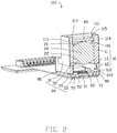
- FIG. 2 is a cross-sectional view of the optical projection device of FIG. 1 along line II-II.
- FIG. 3 is an exploded view of the optical projection device of FIG. 1 .
- FIG. 4 is a view of a metal component of the optical projection device of FIG. 1 from another angle.
- FIGS. 1-4 show an optical projection device 100 .
- the optical projection device 100 includes a holder 10 , a lens 20 , two metal components 30 , a DOE 40 , a printed circuit board 50 , a laser 60 , and a plurality of electric components 70 .
- the lens 20 and the DOE 40 are received in the holder 10 .
- the two metal components 30 are opposite to each other and each are formed on the holder 10 or embedded in the holder 10 .
- the laser 60 and the plurality of electric components 70 are formed on the printed circuit board 50 and received in the holder 10 .
- the laser 60 faces the lens 20 .
- the holder 10 includes a lens cone 11 and a base 12 .
- the lens cone 11 is formed on the base 12 .
- the lens cone 11 includes a first surface 111 , a second surface 112 opposite to the first surface 111 , a first outside surface 113 vertically connecting each of the first surface 111 and the second surface 112 , and a second outside surface 114 opposite to the first outside surface 113 .
- a DOE receiving groove 115 extends from the first surface 111 to an interior of the lens cone 11 .
- a lens receiving groove 116 extends from the second surface 112 to the interior of the lens cone 11 .
- the lens receiving groove 116 is connected to the DOE receiving groove 115 .
- a diameter of the DOE receiving groove 115 is larger than a diameter of the lens receiving groove 116 .
- a step part 117 is formed between the DOE receiving groove 115 and the lens receiving groove 116 .
- each of two first connecting block receiving grooves 118 is formed to extend from the first surface 111 to the interior of the lens cone 11 .
- the two first connecting block receiving grooves 118 are opposite to each other.
- Each of the two first connecting block receiving grooves 118 is connected to the DOE receiving groove 115 .
- a first heat dissipation part groove 119 is formed from the first outside surface 113 and the second outside surface 114 to the DOE receiving groove 115 .
- the first heat dissipation part groove 119 runs through the first outside surface 113 or the second outside surface 114 .
- the first heat dissipation part groove 119 is connected to the DOE receiving groove 115 by the first connecting blocks receiving groove 118 .
- the base 12 includes a third surface 121 opposite to the second surface 112 .
- An electric component receiving groove 122 is formed from the third surface 121 to the second surface 112 .
- the electric component receiving groove 122 is connected to the lens receiving groove 116 .
- the lens cone 11 and the base 12 are integrally formed. In another embodiment, the lens cone 11 can be connected to the base 12 by screws or adhesive.
- the holder 10 further includes a connecting receiving groove 13 .
- the connecting receiving groove 13 is connected to the lens receiving groove 116 , the first heat dissipation part grooves 119 , and the electric component receiving groove 122 .
- the lens 20 is received in the lens receiving groove 116 .
- the lens 20 includes a first ophthalmic lens 21 and a second ophthalmic lens 22 .
- the first ophthalmic lens 21 abuts the first surface 111 .
- the second ophthalmic lens 22 abuts the second surface 112 .
- Each of the two metal components 30 includes a first heat dissipation part 31 , a connecting part 32 , a second heat dissipation part 33 , and an extending part 34 .
- the connecting part 32 is perpendicularly connected to the first heat dissipation part 31 and the second heat dissipation part 33 .
- the extending part 34 extends out from junction of the second heat dissipation part 33 and the connecting part 32 to a direction perpendicular to the second heat dissipation part 33 .
- Each of the first heat dissipation parts 31 includes a gap 311 .
- the gap 311 is away from the connecting part 32 and opposite to the first connecting block receiving groove 118 .
- Two first connecting blocks 312 are perpendicular to the first heat dissipation parts 31 .
- One end of each of the first connecting blocks 312 is defined at each of the gaps 311 .
- the first connecting block 312 and the second heat dissipation part 33 lie on a same side of the connecting part 32 .
- a part of the first heat dissipation part 31 is separated and bent to form the first connecting blocks 312 and the gaps 311 .
- the first connecting block 312 is received in the first connecting blocks receiving groove 118 .
- Two second connecting blocks 35 extend out from the second heat dissipation part 33 and away from the first heat dissipation part 31 .
- the two second connecting blocks 35 are perpendicular to the second heat dissipation part 33 .
- the second connecting block 35 and the extending part 34 lie on different side of the second heat dissipation part 33 .
- a light-passage 341 is formed on and runs through the extending part 34 .
- the light-passage 341 is arc-shaped. In at least one embodiment, the light-passage 341 is semi-arc-shaped.
- the first heat dissipation parts 31 are fixed in the first heat dissipation part grooves 119 .
- the first connecting blocks 312 are received in the first connecting block receiving grooves 118 .
- the connecting part 32 is received in the connecting receiving groove 13 .
- the second heat dissipation parts 33 are fixed in the inner wall of the electric component receiving groove 122 .
- the extending parts 34 are received in the electric component receiving groove 122 and face the laser 60 .
- the two metal components 30 are opposite to each other.
- the light-passages 341 face the second ophthalmic lens 22 .
- the second connecting blocks 35 are fixed on the third surface 121 and exposed outside the base 12 .
- a light-absorbing layer 36 is formed on the second heat dissipation part 33 and the extending part 34 .
- the light-absorbing layer 36 faces the laser 60 .
- the light-absorbing layer 36 prevents reflection of light emitted by the laser 60 , further avoiding stray light affecting the quality of the projected light.
- the metal components 30 are embedded in the holder 10 by insert molding technology.
- the DOE 40 is received in the DOE receiving groove 115 and fixed on the step part 117 .
- the DOE 40 shapes laser beams, for homogenization, collimation, focusing, forming specific patterns, and so on.
- the DOE 40 is electrically connected to the first connecting blocks 312 by two first conducting resins 41 .
- the holder 10 is fixed on the printed circuit board 50 by an adhesive layer 80 .
- the two second connecting blocks 35 are electrically connected to the printed circuit board 50 by a second conducting resin 90 .
- the layer 60 is received in the electric component receiving groove 122 and faces the second ophthalmic lens 22 .
- the layer 60 is electrically connected to the printed circuit board 50 .
- the layer 60 emits light. The light passes through the light-passages 341 and enters into the second ophthalmic lens 22 and the first ophthalmic lens 21 , and then passes through the DOE 40 as projected light.
- the plurality of electric components 70 is received in the electric component receiving groove 122 and electrically connected to the printed circuit board 50 .
- the optical projection device 100 also includes a ceramic substrate 51 and a stiffening plate 52 .
- the ceramic substrate 51 and the stiffening plate 52 are both formed on the printed circuit board 50 and opposite to each other.
- the laser 60 and the plurality of electric components 70 are fixed on the ceramic substrate 51 .
- the ceramic substrate 51 assists the metal components 70 to dissipate heat.
- the metal components 30 are embedded in the holder 10 by insert molding technology, the metal components 30 can dissipate heat generated by the laser 60 and the plurality of electric components 70 to ambient environment.
- the light-absorbing layer 36 is formed on the second heat dissipation part 33 and the extending part 34 to prevent reflection of light emitted by the laser.
- the metal components 30 are replacements for metal pins to realize miniaturization of the optical projection device 100 and reduce utilized space.
- the metal components 30 enhance structural strength of the optical projection device 100 .
Landscapes
- Engineering & Computer Science (AREA)
- General Engineering & Computer Science (AREA)
- Physics & Mathematics (AREA)
- General Physics & Mathematics (AREA)
- Microelectronics & Electronic Packaging (AREA)
- Optics & Photonics (AREA)
- Projection Apparatus (AREA)
- Lens Barrels (AREA)
Abstract
Description
Claims (12)
Applications Claiming Priority (3)
| Application Number | Priority Date | Filing Date | Title |
|---|---|---|---|
| CN201810860135.3A CN110794640A (en) | 2018-08-01 | 2018-08-01 | 3D projector |
| CN201810860135.3 | 2018-08-01 | ||
| CN201810860135 | 2018-08-01 |
Publications (2)
| Publication Number | Publication Date |
|---|---|
| US20200041114A1 US20200041114A1 (en) | 2020-02-06 |
| US10627097B2 true US10627097B2 (en) | 2020-04-21 |
Family
ID=69228441
Family Applications (1)
| Application Number | Title | Priority Date | Filing Date |
|---|---|---|---|
| US16/201,946 Active US10627097B2 (en) | 2018-08-01 | 2018-11-27 | Optical projection device |
Country Status (3)
| Country | Link |
|---|---|
| US (1) | US10627097B2 (en) |
| CN (1) | CN110794640A (en) |
| TW (1) | TWI682230B (en) |
Families Citing this family (1)
| Publication number | Priority date | Publication date | Assignee | Title |
|---|---|---|---|---|
| CN113433644B (en) * | 2020-03-20 | 2023-01-17 | 三赢科技(深圳)有限公司 | Lens module |
Citations (2)
| Publication number | Priority date | Publication date | Assignee | Title |
|---|---|---|---|---|
| TWM531101U (en) | 2016-07-18 | 2016-10-21 | Luxnet Corp | Optic emitter heat dissipation structure and optic emitter including the same |
| US20190331988A1 (en) * | 2018-04-25 | 2019-10-31 | Triple Win Technology(Shenzhen) Co.Ltd. | Optical projector module |
Family Cites Families (12)
| Publication number | Priority date | Publication date | Assignee | Title |
|---|---|---|---|---|
| CN100483655C (en) * | 2005-09-09 | 2009-04-29 | 鸿富锦精密工业(深圳)有限公司 | Producing process for digital camera module |
| CN101364585B (en) * | 2008-09-25 | 2010-10-13 | 旭丽电子(广州)有限公司 | Chip packaging construction and manufacturing method therefor |
| JP2013068873A (en) * | 2011-09-26 | 2013-04-18 | Seiko Epson Corp | Electro-optical module and electronic apparatus |
| JP2014197166A (en) * | 2013-03-07 | 2014-10-16 | セイコーエプソン株式会社 | Optical element, method for manufacturing optical element, and projector |
| CN105338737B (en) * | 2014-07-18 | 2019-02-12 | 南昌欧菲光电技术有限公司 | Circuit board assemblies and mobile phone camera mould group |
| TWI540463B (en) * | 2015-02-04 | 2016-07-01 | 奇鋐科技股份有限公司 | The projection structure of input interface and the electronic devices having the projection structure |
| JP6381830B2 (en) * | 2015-11-09 | 2018-08-29 | 三菱電機株式会社 | Projection optical equipment and headlamp device |
| US10362295B2 (en) * | 2016-09-19 | 2019-07-23 | Apple Inc. | Optical apparatus with beam steering and position feedback |
| KR102622721B1 (en) * | 2016-12-05 | 2024-01-09 | 삼성전자주식회사 | Display apparatus |
| CN107240861A (en) * | 2017-07-18 | 2017-10-10 | 杭州大湛机电科技有限公司 | Nanometer water ion generating device and refrigeration unit preparation method based on refrigeration unit |
| CN207456385U (en) * | 2017-11-30 | 2018-06-05 | 深圳奥比中光科技有限公司 | Projection module with Beam Monitoring unit |
| CN207518758U (en) * | 2017-12-14 | 2018-06-19 | 技嘉科技股份有限公司 | Video capturing device |
-
2018
- 2018-08-01 CN CN201810860135.3A patent/CN110794640A/en active Pending
- 2018-11-27 US US16/201,946 patent/US10627097B2/en active Active
- 2018-12-05 TW TW107143783A patent/TWI682230B/en active
Patent Citations (2)
| Publication number | Priority date | Publication date | Assignee | Title |
|---|---|---|---|---|
| TWM531101U (en) | 2016-07-18 | 2016-10-21 | Luxnet Corp | Optic emitter heat dissipation structure and optic emitter including the same |
| US20190331988A1 (en) * | 2018-04-25 | 2019-10-31 | Triple Win Technology(Shenzhen) Co.Ltd. | Optical projector module |
Also Published As
| Publication number | Publication date |
|---|---|
| CN110794640A (en) | 2020-02-14 |
| TW202008070A (en) | 2020-02-16 |
| US20200041114A1 (en) | 2020-02-06 |
| TWI682230B (en) | 2020-01-11 |
Similar Documents
| Publication | Publication Date | Title |
|---|---|---|
| US20220137322A1 (en) | Optical element driving mechanism | |
| US10197242B2 (en) | Lens arrays and mountings | |
| TWI735232B (en) | Light emitter and light detector modules and method of fabricating the same | |
| US9696008B2 (en) | Reflector for directed beam LED illumination | |
| US20170131560A1 (en) | Diffractive optical element and laser diode-doe module | |
| US10605423B2 (en) | Device for positioning a module comprising a light source on an optical device | |
| US10627097B2 (en) | Optical projection device | |
| US7076145B2 (en) | Light tunnel retention and adjustment apparatus | |
| US20110122511A1 (en) | Lens unit | |
| US10645352B2 (en) | Optical projection module | |
| US9645408B2 (en) | Surface mount device type laser module | |
| US8736738B2 (en) | Optical lens and image pick-up apparatus having same | |
| JP2023160869A (en) | Illuminating device | |
| US10743415B2 (en) | Camera module with reduced light leakage and electronic device using same | |
| US10222687B2 (en) | Light homogenizing device and laser projection apparatus | |
| US20220179163A1 (en) | Optical element driving mechanism | |
| US10712642B2 (en) | Optical projection module with improved heat dissipation | |
| US11375093B2 (en) | Optical member driving device, camera device, and electronic apparatus | |
| US11181712B2 (en) | Lens module and electronic device having the same | |
| US10330528B2 (en) | Optical assembly position adjustment device | |
| CN107797195B (en) | Optical assembly positioning adjustment device | |
| CN213904786U (en) | Display device | |
| TWM544025U (en) | Backlight module and display device | |
| US20230170645A1 (en) | Electrical connector | |
| US20110001938A1 (en) | Optical projection system |
Legal Events
| Date | Code | Title | Description |
|---|---|---|---|
| AS | Assignment |
Owner name: TRIPLE WIN TECHNOLOGY(SHENZHEN) CO.LTD., CHINA Free format text: ASSIGNMENT OF ASSIGNORS INTEREST;ASSIGNORS:DING, SHENG-JIE;CHEN, SHIN-WEN;LI, JING-WEI;AND OTHERS;REEL/FRAME:047597/0329 Effective date: 20181106 |
|
| FEPP | Fee payment procedure |
Free format text: ENTITY STATUS SET TO UNDISCOUNTED (ORIGINAL EVENT CODE: BIG.); ENTITY STATUS OF PATENT OWNER: LARGE ENTITY |
|
| STPP | Information on status: patent application and granting procedure in general |
Free format text: NOTICE OF ALLOWANCE MAILED -- APPLICATION RECEIVED IN OFFICE OF PUBLICATIONS |
|
| STCF | Information on status: patent grant |
Free format text: PATENTED CASE |
|
| MAFP | Maintenance fee payment |
Free format text: PAYMENT OF MAINTENANCE FEE, 4TH YEAR, LARGE ENTITY (ORIGINAL EVENT CODE: M1551); ENTITY STATUS OF PATENT OWNER: LARGE ENTITY Year of fee payment: 4 |