US10622180B2 - Method for producing an electron emitter coated with a nanorod-containing coating - Google Patents
Method for producing an electron emitter coated with a nanorod-containing coating Download PDFInfo
- Publication number
- US10622180B2 US10622180B2 US16/348,061 US201716348061A US10622180B2 US 10622180 B2 US10622180 B2 US 10622180B2 US 201716348061 A US201716348061 A US 201716348061A US 10622180 B2 US10622180 B2 US 10622180B2
- Authority
- US
- United States
- Prior art keywords
- nanorods
- adhesive layer
- carbon nanotubes
- electron emitter
- average
- Prior art date
- Legal status (The legal status is an assumption and is not a legal conclusion. Google has not performed a legal analysis and makes no representation as to the accuracy of the status listed.)
- Active
Links
Images


Classifications
-
- C—CHEMISTRY; METALLURGY
- C01—INORGANIC CHEMISTRY
- C01B—NON-METALLIC ELEMENTS; COMPOUNDS THEREOF; METALLOIDS OR COMPOUNDS THEREOF NOT COVERED BY SUBCLASS C01C
- C01B32/00—Carbon; Compounds thereof
- C01B32/15—Nano-sized carbon materials
- C01B32/158—Carbon nanotubes
-
- C—CHEMISTRY; METALLURGY
- C01—INORGANIC CHEMISTRY
- C01B—NON-METALLIC ELEMENTS; COMPOUNDS THEREOF; METALLOIDS OR COMPOUNDS THEREOF NOT COVERED BY SUBCLASS C01C
- C01B32/00—Carbon; Compounds thereof
- C01B32/15—Nano-sized carbon materials
- C01B32/158—Carbon nanotubes
- C01B32/16—Preparation
-
- C—CHEMISTRY; METALLURGY
- C01—INORGANIC CHEMISTRY
- C01B—NON-METALLIC ELEMENTS; COMPOUNDS THEREOF; METALLOIDS OR COMPOUNDS THEREOF NOT COVERED BY SUBCLASS C01C
- C01B32/00—Carbon; Compounds thereof
- C01B32/15—Nano-sized carbon materials
- C01B32/158—Carbon nanotubes
- C01B32/168—After-treatment
-
- C—CHEMISTRY; METALLURGY
- C09—DYES; PAINTS; POLISHES; NATURAL RESINS; ADHESIVES; COMPOSITIONS NOT OTHERWISE PROVIDED FOR; APPLICATIONS OF MATERIALS NOT OTHERWISE PROVIDED FOR
- C09D—COATING COMPOSITIONS, e.g. PAINTS, VARNISHES OR LACQUERS; FILLING PASTES; CHEMICAL PAINT OR INK REMOVERS; INKS; CORRECTING FLUIDS; WOODSTAINS; PASTES OR SOLIDS FOR COLOURING OR PRINTING; USE OF MATERIALS THEREFOR
- C09D1/00—Coating compositions, e.g. paints, varnishes or lacquers, based on inorganic substances
-
- C—CHEMISTRY; METALLURGY
- C09—DYES; PAINTS; POLISHES; NATURAL RESINS; ADHESIVES; COMPOSITIONS NOT OTHERWISE PROVIDED FOR; APPLICATIONS OF MATERIALS NOT OTHERWISE PROVIDED FOR
- C09D—COATING COMPOSITIONS, e.g. PAINTS, VARNISHES OR LACQUERS; FILLING PASTES; CHEMICAL PAINT OR INK REMOVERS; INKS; CORRECTING FLUIDS; WOODSTAINS; PASTES OR SOLIDS FOR COLOURING OR PRINTING; USE OF MATERIALS THEREFOR
- C09D5/00—Coating compositions, e.g. paints, varnishes or lacquers, characterised by their physical nature or the effects produced; Filling pastes
- C09D5/20—Coating compositions, e.g. paints, varnishes or lacquers, characterised by their physical nature or the effects produced; Filling pastes for coatings strippable as coherent films, e.g. temporary coatings strippable as coherent films
-
- C—CHEMISTRY; METALLURGY
- C09—DYES; PAINTS; POLISHES; NATURAL RESINS; ADHESIVES; COMPOSITIONS NOT OTHERWISE PROVIDED FOR; APPLICATIONS OF MATERIALS NOT OTHERWISE PROVIDED FOR
- C09J—ADHESIVES; NON-MECHANICAL ASPECTS OF ADHESIVE PROCESSES IN GENERAL; ADHESIVE PROCESSES NOT PROVIDED FOR ELSEWHERE; USE OF MATERIALS AS ADHESIVES
- C09J9/00—Adhesives characterised by their physical nature or the effects produced, e.g. glue sticks
- C09J9/02—Electrically-conducting adhesives
-
- H—ELECTRICITY
- H01—ELECTRIC ELEMENTS
- H01J—ELECTRIC DISCHARGE TUBES OR DISCHARGE LAMPS
- H01J1/00—Details of electrodes, of magnetic control means, of screens, or of the mounting or spacing thereof, common to two or more basic types of discharge tubes or lamps
- H01J1/02—Main electrodes
- H01J1/30—Cold cathodes, e.g. field-emissive cathode
- H01J1/304—Field-emissive cathodes
- H01J1/3042—Field-emissive cathodes microengineered, e.g. Spindt-type
- H01J1/3044—Point emitters
-
- H—ELECTRICITY
- H01—ELECTRIC ELEMENTS
- H01J—ELECTRIC DISCHARGE TUBES OR DISCHARGE LAMPS
- H01J9/00—Apparatus or processes specially adapted for the manufacture, installation, removal, maintenance of electric discharge tubes, discharge lamps, or parts thereof; Recovery of material from discharge tubes or lamps
- H01J9/02—Manufacture of electrodes or electrode systems
- H01J9/022—Manufacture of electrodes or electrode systems of cold cathodes
- H01J9/025—Manufacture of electrodes or electrode systems of cold cathodes of field emission cathodes
-
- B—PERFORMING OPERATIONS; TRANSPORTING
- B82—NANOTECHNOLOGY
- B82Y—SPECIFIC USES OR APPLICATIONS OF NANOSTRUCTURES; MEASUREMENT OR ANALYSIS OF NANOSTRUCTURES; MANUFACTURE OR TREATMENT OF NANOSTRUCTURES
- B82Y10/00—Nanotechnology for information processing, storage or transmission, e.g. quantum computing or single electron logic
-
- B—PERFORMING OPERATIONS; TRANSPORTING
- B82—NANOTECHNOLOGY
- B82Y—SPECIFIC USES OR APPLICATIONS OF NANOSTRUCTURES; MEASUREMENT OR ANALYSIS OF NANOSTRUCTURES; MANUFACTURE OR TREATMENT OF NANOSTRUCTURES
- B82Y30/00—Nanotechnology for materials or surface science, e.g. nanocomposites
-
- B—PERFORMING OPERATIONS; TRANSPORTING
- B82—NANOTECHNOLOGY
- B82Y—SPECIFIC USES OR APPLICATIONS OF NANOSTRUCTURES; MEASUREMENT OR ANALYSIS OF NANOSTRUCTURES; MANUFACTURE OR TREATMENT OF NANOSTRUCTURES
- B82Y40/00—Manufacture or treatment of nanostructures
-
- C—CHEMISTRY; METALLURGY
- C01—INORGANIC CHEMISTRY
- C01B—NON-METALLIC ELEMENTS; COMPOUNDS THEREOF; METALLOIDS OR COMPOUNDS THEREOF NOT COVERED BY SUBCLASS C01C
- C01B2202/00—Structure or properties of carbon nanotubes
- C01B2202/06—Multi-walled nanotubes
-
- C—CHEMISTRY; METALLURGY
- C01—INORGANIC CHEMISTRY
- C01B—NON-METALLIC ELEMENTS; COMPOUNDS THEREOF; METALLOIDS OR COMPOUNDS THEREOF NOT COVERED BY SUBCLASS C01C
- C01B2202/00—Structure or properties of carbon nanotubes
- C01B2202/20—Nanotubes characterized by their properties
- C01B2202/22—Electronic properties
-
- C—CHEMISTRY; METALLURGY
- C01—INORGANIC CHEMISTRY
- C01B—NON-METALLIC ELEMENTS; COMPOUNDS THEREOF; METALLOIDS OR COMPOUNDS THEREOF NOT COVERED BY SUBCLASS C01C
- C01B2202/00—Structure or properties of carbon nanotubes
- C01B2202/20—Nanotubes characterized by their properties
- C01B2202/34—Length
-
- C—CHEMISTRY; METALLURGY
- C01—INORGANIC CHEMISTRY
- C01B—NON-METALLIC ELEMENTS; COMPOUNDS THEREOF; METALLOIDS OR COMPOUNDS THEREOF NOT COVERED BY SUBCLASS C01C
- C01B2202/00—Structure or properties of carbon nanotubes
- C01B2202/20—Nanotubes characterized by their properties
- C01B2202/36—Diameter
-
- C—CHEMISTRY; METALLURGY
- C01—INORGANIC CHEMISTRY
- C01P—INDEXING SCHEME RELATING TO STRUCTURAL AND PHYSICAL ASPECTS OF SOLID INORGANIC COMPOUNDS
- C01P2004/00—Particle morphology
- C01P2004/10—Particle morphology extending in one dimension, e.g. needle-like
- C01P2004/13—Nanotubes
- C01P2004/133—Multiwall nanotubes
-
- H—ELECTRICITY
- H01—ELECTRIC ELEMENTS
- H01J—ELECTRIC DISCHARGE TUBES OR DISCHARGE LAMPS
- H01J2201/00—Electrodes common to discharge tubes
- H01J2201/30—Cold cathodes
- H01J2201/304—Field emission cathodes
- H01J2201/30403—Field emission cathodes characterised by the emitter shape
- H01J2201/30434—Nanotubes
-
- H—ELECTRICITY
- H01—ELECTRIC ELEMENTS
- H01J—ELECTRIC DISCHARGE TUBES OR DISCHARGE LAMPS
- H01J2201/00—Electrodes common to discharge tubes
- H01J2201/30—Cold cathodes
- H01J2201/304—Field emission cathodes
- H01J2201/30446—Field emission cathodes characterised by the emitter material
- H01J2201/30453—Carbon types
- H01J2201/30476—Diamond-like carbon [DLC]
Definitions
- the invention relates to a method for producing electron emitters coated with a coating containing nanorods, in particular carbon nanotubes.
- the invention further relates to electron emitters which can be produced by the proposed method and are provided in particular for use as cathodes of x-ray tubes.
- Nanorods are understood as meaning both solid and hollow rod-shaped particles. Nanorods, if they are not hollow, are also called nanosticks. Otherwise, they are nanotubes. Nanotubes formed of carbon, that is, carbon nanotubes, are referred to as CNTs (carbon nanotubes) for short.
- Carbon nanotubes have a variety of technical application potentials; an overview and outlook is summarized in: Kanian Balasubramanian, Marko Burghard, “buchalinstrumente Kohlenstoff-Nanorschreiben [in English: Functionalized carbon nanotubes ]”, Chemie in 102, Vol. 39, pp. 16 to 25 and in: Andreas Hirsch, “The era of carbon allotropes”, Nature Materials, 2010, vol. 9, pp. 868-871.
- Carbon nanotubes are approximately cylindrical molecules whose walls, like the planes of graphite, consist of carbon, the carbon atoms on the lateral surface having a honeycomb-like structure with hexagons.
- Carbon nanotubes can be open or closed tubes; in the case of closed carbon nanotubes their closed ends differ from the graphite structure of the cylindrical walls and transition into a fullerene structure.
- one carbon atom is covalently linked to three further carbon atoms on the lateral surfaces and at closed ends.
- the carbon atoms at the respective end are covalently linked to less than three bonding partners.
- the diameter of the carbon nanotubes is in the range of 0.3 to 200 nm. Lengths of several millimeters for single carbon nanotubes and up to 20 cm for bundles of carbon nanotubes have already been achieved.
- carbon nanotubes other free atoms and molecules may be included, for example noble gases, metal atoms and metal clusters, carbon dioxide and alkanes.
- Multi-walled carbon nanotubes comprise those carbon nanotubes in which at least one additional carbon nanotube is included as a separate molecule.
- Carbon nanotubes may also have heteroatoms, especially nitrogen, and be functionalized with a variety of inorganic and organic radicals.
- FIGS. 4, 6 Various embodiments of the proposed electron emitter and an unclaimed comparison example ( FIGS. 4, 6 ) will be explained in more detail below with reference to a drawing.
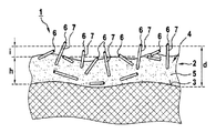
- FIG. 1 shows a cross section through an electron emitter 1 with a coating 2 containing carbon nanotubes
- FIG. 4 shows an unclaimed electron emitter 1 in a view in analogy to FIG. 3 ,
- FIG. 5 shows a three-dimensional view of electron emitter 1 according to FIG. 3 .
- FIG. 6 shows electron emitter 1 of FIG. 4 in a view according to FIG. 5 .
- FIG. 7 shows electron emitter 1 according to FIGS. 1, 3 and 5 in a further three-dimensional, realistic representation
- FIG. 8 shows electron emitter 1 according to FIG. 1 in plan view
- FIG. 9 shows a measured profile of electron emitter 1 according to FIG. 7 .
- FIG. 10 shows electron micrographs of electron emitter 1 according to FIG. 7 .
- FIG. 11 in a diagram shows characteristic curves of three electron emitters 1 of the same design
- FIG. 13 in a diagram shows the emission stability of the three electron emitters 1 according to FIG. 11 ,
- FIG. 14 shows measured operating parameters of electron emitter 1 of FIG. 11 .
- FIG. 15 in a diagram in analogy to FIG. 13 shows the measured operating behavior of a further electron emitter 1 .
- FIG. 16 shows current and voltage values measured during a pulse of 250 ms duration during operation of electron emitter 1 according to FIG. 15 .
- carbon nanotubes have a very low field strength threshold of less than 2 V ⁇ m ⁇ 1 for the emission of electrons by an electric field. Therefore, carbon nanotubes are well-suited as components for electron emitters, as for example generally proposed in DE 603 05 371 T2 for a plasma display device, in US 2004 0070326 A1 for a field emission display device and in U.S. Pat. No. 6,914,372 B1 as well as in U.S. Pat. No. 6,097,138 for an electron emitter.
- carbon nanotubes are suitable as cathode material for X-ray tubes, as disclosed, for example, in DE 10 2008 052 363 A1, DE 11 2012 004 856 T5, DE 10 2010 012 394 A1, DE 10 2009 049 663 A1 and DE 10 2009 040 769 A1.
- X-ray generation using carbon nanotubes Nano Convergence (2015)2: 1.
- Information on CNTs beyond the technical field of electron emitters can be found in the publication: M. S. Fuhrer, Single-Walled Carbon Nanotubes for Nanoelectronics, Advanced Semiconductor and Organic Nano-Techniques (Part II).
- the field strength threshold for cathodes for emitting electrons having carbon nanotubes can be further lowered by arranging them in a perpendicular preferential direction on the emitter surface.
- multi-walled carbon nanotubes are particularly suitable for electron emitter applications, as outlined in the paper: Lo ⁇ ck-Alexandre Gautier, Vincent Le Borgne, Samir Al Moussalami, My Ali El Khakani, “Enhanced field electron emission properties of hierarchically structured MWCNT-based cold cathodes”, Nanoscale Research Letters, 2014, vol. 9, edition, p. 55 et seq. and in paper: Alexander A. Kuznetzov, Sergey B. Lee, Mei Zhang, Ray H. Baughman, Anvar A. Zakhidov, “Electron field emission from transparent multiwalled carbon nanotube sheets for inverted field emission displays”, CARBON, 2010, vol. 48, pp. 41 to 48.
- the electrical sheet resistance R F should vary as little as possible.
- the electrical sheet resistance R F of a resistive layer is given by the ratio of the electrical isotropic resistivity ⁇ to the layer thickness of the resistive layer; the unit of electrical sheet resistance R F is therefore identical to the unit of electrical resistance ⁇ (ohms).
- the carbon nanotubes are applied to the surface in individual matrix elements. These matrix elements must first be produced separately and thus at high cost by growing carbon nanotubes or by a sintering operation. Furthermore, these matrix elements may only contain less than 5% by volume of carbon nanotubes. Otherwise, these matrix elements are excessively brittle. No further details with respect to the components of the sintered body and the actual sintering operation with respect to the matrix elements are provided in DE 10 2008 052 363 A1; definite chemical compounds, mixing ratios and definite process conditions are not disclosed.
- EP 1 957 397 B1 describes a method for producing electron emitters with a coating containing carbon nanotubes. This method relies on applying a paste containing carbon nanotubes, an organic binder, metal particles and solvents. The paste is applied to the overall coating region and then either cured or annealed by polymerization. However, EP 1 957 397 B1 does not disclose the composition of the organic binder.
- DE 602 21 951 T2 likewise describes a photolithographic method for producing electron emitters with a coating containing carbon nanotubes. This method is also based on applying a paste containing carbon nanotubes, alkali silicate and a binder.
- the adhesive layer should then have an organic binder and carbon nanotubes as constituents.
- an adhesive film for example a commercially available adhesive strip for do it yourself (DIY) or office use, is successively pressed and pulled off again at each location of the coating region.
- DIY do it yourself
- a proportion of the coating surface which consists of loose material and contaminants, is removed.
- the layer thickness of the coating is reduced. This treatment results in a surface with carbon nanotubes protruding upright, that is, oriented in the perpendicular preferential direction.
- the results of this method are not sufficiently reproducible with respect to the number of upright carbon nanotubes per unit surface.
- Even shallow depressions in the coating region concerned have contaminants, wherein surface-protruding and upright carbon nanotubes cannot be found in the depressions. This results in a very irregularly structured overall coating region.
- the coating produced by this method does not have the required temperature resistance of at least 500° C. for technical uses, for example as cathodes in electron emitters.
- the method of claim 1 includes the use of nanorods for producing an electron emitter.
- the electron emitter according to claim 15 comprises nanorods as constituents of a coating.
- the nanorods of the electron emitter may have a uniform or non-uniform composition and may be formed either as hollow bodies, i.e., as tubes, or solid.
- the nanorods in particular nanotubes, can be formed from metal oxides.
- titanium oxide (TiO 2 ), zinc oxide (ZnO) and aluminum oxide (Al 2 O 3 ) are mentioned and named as materials from which nanotubes may be formed.
- Metal oxides for example titanium oxide, zinc oxide or manganese oxide (Mn x O y ), both in pure and in doped form, are suitable for producing the emitter according to the invention.
- metals, sulfides, nitrides or carbides, either in pure or in doped form may be present.
- rod-shaped, optionally hollow, elements made of polymeric materials are also suitable.
- carbon nanotubes or nanotubes made of other materials for example oxides or nitrides, filled or doped with a metallic or ceramic material, for example with nitrogen (N), gold (Au) or europium (Eu, are suitable for use in the electron emitter coating provided for emission of electrons.
- a metallic or ceramic material for example with nitrogen (N), gold (Au) or europium (Eu)
- N nitrogen
- Au gold
- Eu europium
- nanorods In embodiments in which carbon nanotubes, especially exclusively consisting of carbon, are used as nanorods, said nanorods have, for example, an outer diameter of 0.4 nm to 20 nm and a length of 1 ⁇ m to 20 ⁇ m.
- a general reference to carbon nanotubes in the following description includes single-walled and multi-walled, double-sided or one-sided open or closed carbon nanotubes in mixed and pure form, regardless of their respective production method.
- the proposed method for producing an electron emitter with a coating containing carbon nanotubes on a component surface comprises the following steps:
- FIG. 1 shows a cross section through a region of the overall coating region of electron emitter 1 , which was produced by the exemplary method steps (I) to (IV) set out above.
- Coating 2 on component surface 3 has carbon nanotubes 4 , wherein coating 2 contains multi-walled carbon nanotubes with an outer diameter of 2 nm to 20 nm and a length of 1 ⁇ m to 10 ⁇ m.
- Coating 2 with an average coating thickness d of 13 ⁇ m consists of electrically conductive adhesive layer 5 with an average partial layer thickness h of 10 ⁇ m and carbon nanotubes with the ends 6 protruding from the adhesive layer. Ends 6 of the carbon nanotubes have an average differential distance i of 3 ⁇ m to adhesive layer 5 .
- average coating thickness d is composed of the sum of partial layer thickness h and the mean differential distance i. Parameters d, h and i extend over the overall coating region.
- Electron emitter 1 has, over the overall coating region, an average number n of carbon nanotubes 7 of 10 5 per mm 2 protruding from the electrically conductive adhesive layer and predominantly with an upright orientation, as well as an average electrical sheet resistance R FM of 0.5 ⁇ .
- the parameters n and R FM thus also extend over the overall coating region.
- adhesive layer 5 has multi-walled carbon nanotubes with an outer diameter of 2 nm to 20 nm and a length of 1 ⁇ m to 10 ⁇ m, single-walled carbon nanotubes with an outer diameter of 0.4 nm to 4 nm and a length of 1 ⁇ m to 10 ⁇ m, other components made of carbon, silver particles and silicon carbide.
- adhesive layer 5 contains glass particles which are sintered together in at least one point of contact.
- Adhesive layer 5 is firmly bonded by sintering the glass articles on the surface of the device.
- the carbon nanotubes are firmly embedded between these sintered glass particles.
- Coating 2 has a thermal stability of 650° C.
- suitable metals are molybdenum (Mo), tungsten (W), nickel (Ni) and copper (Cu).
- suitable metal alloys are stainless steels.
- iron (Fe) alloys are suitable which contain cobalt or nickel or palladium or platinum or nickel and cobalt (Co) as further constituents and preferably have a coefficient of thermal expansion of not more than 5 ppm K ⁇ 1 .
- suitable glasses are silicate glasses and borate glasses with a transformation range above 850° C.
- suitable ceramics are fired clay, porcelain, magnesium oxide (MgO), boron carbide (B 4 C), boron nitride, aluminum nitride, aluminum oxide (Al 2 O 3 ), boron-aluminum and titanium-aluminum and zirconium-aluminum mixed oxides, zirconium oxide (ZrO 2 ), mullite (porcelainite or 3 Al 2 O 3 2 Si O 2 or 2Al 2 O 3 SiO 2 ), silicon carbide and borides, silicides and titanates.
- the proposed method can also be used to coat one or more coatings on the surface of a component which is provided as a component for the electron emitter.
- the proposed method can be used to coat a surface of a coating of tungsten, molybdenum, silver, a silver-platinum alloy, a silver-palladium alloy, gold, a gold-platinum alloy, a gold-palladium alloy, platinum, palladium, carbon, copper or an iron-nickel alloy, which is applied to alumina.
- the electrical adhesive layer contains such particles which are sintered together in at least one point of contact.
- the adhesive layer is also firmly bound by sintering these particles on the surface of the component.
- the carbon nanotubes are firmly embedded between these sintered particles.
- the required contact for electrical conduction between the applied carbon nanotubes is imparted by the adhesive layer.
- the adhesive layer thus contributes to an average electrical surface conductivity over the overall coating region.
- the electrical conductivity within the adhesive layer is imparted by mutually contacting carbon nanotubes.
- the inorganic and electrically conductive adhesive layer has a thermal stability of at least 600° C. This temperature is 100° C. higher than the maximum temperature, which is usually achieved in at least one manufacturing step of the electron emitter.
- the inorganic and electrically conductive adhesive layer can be produced by, for example, firing a layer.
- This adhesive layer then contains sinterable particles, carbon nanotubes and optionally additional conductive particles 8 .
- the firing temperature is chosen so that the sintering of the sinterable particles takes place without formation of a melt; the nanorods, in particular carbon nanotubes, as well as optionally added further electrically conductive particles 8 do not decompose, but complete decomposition or volatilization of all organic constituents of the layer applied in the method step (I) is ensured.
- the nanorods preferably present in the form of carbon nanotubes are randomly distributed in the electrically conductive adhesive layer prior to method step (IV). Before method step (IV), only a negligible number of nanorods protrude from the adhesive layer.
- the sinterable particles are sintered just so firmly together that in method step (IV) only the portion of the coating surface is removed, which consists of loose material and contaminants.
- a surface is obtained from which carbon nanotubes or other nanorods with an anisotropic preferential direction protrude perpendicular to the substrate surface.
- Particles in particular those made of inorganic oxides, mixed oxides and inorganic oxide mixtures, have proven to be suitable sinterable particles.
- Suitable oxides include, for example, silica, alkali-containing silica, tin oxide, lead oxide, boron oxide and alumina, and mixed oxides and mixtures thereof.
- Suitable additional electrically conductive particles 8 include, for example, particles made of conductive carbon, such as carbon black, graphite or graphene, or particles of indium tin oxide (ITO) or metal particles, such as those made of silver (Ag), gold (Au), tungsten (W), iron (Fe) or nickel (Ni), and mixtures thereof.
- conductive carbon such as carbon black, graphite or graphene
- ITO indium tin oxide
- metal particles such as those made of silver (Ag), gold (Au), tungsten (W), iron (Fe) or nickel (Ni), and mixtures thereof.
- a paste containing nanorods, in particular carbon nanotubes, and sinterable particles is applied to the device by means of screen printing and then fired to form an inorganic and electrically conductive adhesive layer.
- the sinterable particles are sintered together in at least one point of contact and impart adhesion on the surface of the device.
- the sinterable particles impart the adhesion both of the adhesive layer on the component surface and of the nanorods in the adhesive layer.
- various paste materials can additionally be applied to the surface of the device with the proposed method between the individual method steps (I) to (IV) or preferably after method step (IV) in order to realize further electronic functions.
- This relates not only to electrical conductors but also, for example, to dielectrics, capacitors, resistors, coils, antennas, diodes, transistors, electroluminescent components, biosensors and embedding components in multilayer circuits.
- an electrically insulating material in particular ceramic materials, has proven to be advantageous as a substrate.
- the paste used for screen printing preferably also contains carbide-forming particles, an organic dispersant, an organic solvent and optionally additional conductive particles 8 as functional components.
- the organic dispersant and the organic solvent serve to distribute the carbon nanotubes or other nanorods and all other particles contained.
- the adhesive layer then contains additional conductive particles and carbides.
- Suitable organic dispersants are, for example, polyvinylpyrrolidone, ethyl cellulose, ethylene glycol and sodium dodecylsulfate.
- Suitable organic solvents are, for example, isopropanol, ethanol, acetone, N-methyl-2-pyrrolidone, butyl carbitol acetate, terpineols and dimethylformamide.
- the organic dispersants and organic solvents react particularly advantageously with the carbide-forming particles to form carbides in the firing operation in the method step (I) according to claim 2 . These carbides then improve the adhesion of the resulting inorganic and electrically conductive adhesive layer on the component surface.
- Suitable carbide-forming particles are, for example, silicon, titanium and iron.
- Conductive carbons such as carbon black, graphite or graphene, or particles made of indium tin oxide or metal particles, such as, for example, silver, gold, tungsten, iron or nickel, and mixtures thereof, are particularly suitable as conductive particles 8 additionally optionally added to the paste.
- conductive metal particles may be generated in the adhesive layer by adding metal nitrates to the paste. These nitrates assist in the firing operation in that both the metal cation and the nitrate anion oxidize organic components of the paste. In this process, the respective metal cation is reduced to form the metal. Nitrates of the metals iron, ruthenium, nickel, palladium, platinum, copper, silver and gold have proven to be particularly suitable. In the case of nitrates of the metals iron and ruthenium, the corresponding metal carbides also form.
- Total solids content is composed of the proportions by weight of the nanorods, the conductive particles 8 and the binder.
- the total solids content relative to the total weight of the paste significantly influences the usability of the paste as a screen printing material as well as the packing density of the fired film.
- the paste can still be distributed sufficiently easily in the pores of the printing screen and, on the other hand, the adhesive layer produced by firing is still sufficiently dense. If the total solids content is very high, a particularly dense adhesive layer can be produced; however, a correspondingly high pore size of the screen is required for screen printing. Therefore, a total solids content of 10 to 50% by weight has proven to be advantageous for the proposed method, in particular for generating a high coating thickness of the adhesive layer.
- the average grain size of all the particles contained also affects the sieving ability of the paste and the properties of the fired film. Although very small particles are advantageous for the sieving ability of the paste, excessively small particles lead to an excessively high packing density of the fired film. An average grain size of all particles contained in the paste of 0.1 ⁇ m to 10 ⁇ m has therefore proven to be advantageous for the proposed method.
- a paste has been proven to be particularly advantageous which contains not more than 2% by weight nanorods, in particular carbon nanotubes, a total of not more than 20% by weight of glass particles, additional conductive particles 8 and carbide-forming elements of an average grain size of 0.1 ⁇ m to 5 ⁇ m, up to 48.91% by weight terpineols, up to 20.96% by weight butyl carbitol acetate and up to 8.13% by weight ethyl cellulose.
- such a paste is also suitable for producing three-dimensional conductive workpieces by means of generative production methods, such as, for example, 3D printing.
- the firing of the applied paste to form the adhesive layer is carried out with a stepwise increase in temperature up to 800° C.
- a firing time is chosen, after which the electrically conductive adhesive layer thus produced has only inorganic constituents.
- Suitable polymer mixtures for the method step (II) are those liquid preparations with a crosslinkable polymer and with a crosslinking component which do not dissolve the adhesive layer, do not react with the carbon nanotubes and form an elastomer film in the method step (III).
- the method step (III) takes place thermally or photochemically depending on the chosen polymer mixture.
- the elastomer film is then finally peeled off from the overall coating region in the method step (IV).
- the coating applied in the method step (I) is post-treated particularly advantageously in the method steps (II) to (IV) over the overall coating region, even in hard-to-reach partial regions and deep depressions, in such a way that carbon nanotubes protrude from the adhesive layer with an upright orientation.
- the peeling off (or removing) of the elastomer film in the method step (IV) removes contaminants from the surface of the coating.
- the removal of contaminants and the upright orientation of carbon nanotubes can be achieved on those coating regions which are uneven or have a complex geometry.
- the proposed method is superior to those of the prior art.
- the two components are preferably mixed just before carrying out the method step (II) and applied, for example, either by pouring, brushing or spin coating over the overall coating region.
- it has proven particularly suitable to use polymer mixtures which are thermally cured to an elastomer film in the method step (III).
- Such components for generating the elastomer film are commercially available, for example, in the form of two-component sets called: SYLGRAD 184 from Dow Corning Inc., wherein the component containing the crosslinkable silicone polymer is mixed with the component containing the crosslinking reagent.
- the electrically conductive adhesive layer has an average partial layer thickness h of 3 ⁇ m to 20 ⁇ m and the ends of the nanorods, preferably formed as carbon nanotubes, protruding from the conductive layer have an average differential length i of 0.1 ⁇ m to 10 ⁇ m, wherein the nanorods are firmly connected to the surface of the device via the adhesive layer.
- the average coating thickness d over the overall coating region is composed of the sum of the average partial layer thickness h and the average differential length i and therefore amounts to 3.1 ⁇ m to 30 ⁇ m.
- the electron emitter produced by the proposed method has a high emission performance if said electron emitter contains an average number n of nanorods, in particular carbon nanotubes, protruding from the adhesive layer with a predominantly upright orientation of 10 4 to 10 6 per mm 2 over the overall coating region.
- a predominantly upright orientation of nanorods is therefore understood to mean an orientation in which nanorods applied to the component surface are arranged with a maximum deviation of 45° perpendicular to a tangent at their respective point of attachment.
- the point of attachment is understood to mean the point of intersection of the average geometric longitudinal axis of the respective nanorods with the surface of the substrate.
- the proposed electron emitter per partial coating region of a size of at least 10 ⁇ 8 mm 2 , the coating thickness, the number of nanorods protruding from the adhesive layer with an upright orientation per mm 2 , and the electrical sheet resistance R F do not deviate by more than 25% from the average values d, n and R FM .
- This enables the construction of electron emitters of high constant performance density on the overall coating region of the device. Consequently, the formation of hot spots and flashovers is minimized on the overall coating region due to this very regular surface finish; thus, the proposed electron emitter also has a particularly long useful life.
- the performance of the proposed electron emitter can be further improved if the ratio of the average partial layer thickness h to the mean differential length i is from 1 to 3.
- the electrically conductive adhesive layer has an average partial thickness h of 3 ⁇ m to 15 ⁇ m and the ends of the nanorods, in particular carbon nanotubes, protruding from the adhesive layer have an average differential length i of 3 ⁇ m to 5 ⁇ m.
- the coating contains multi-walled carbon nanotubes with an outer diameter of 2 nm to 20 nm and a length of 1 ⁇ m to 10 ⁇ m.
- multi-walled carbon nanotubes which are produced by an arc discharge method, are used for this purpose.
- Such carbon nanotubes produced by an arc discharge method have a very regular acicular structure with only a few curvatures.
- the following is an exemplary embodiment of the proposed method for producing an electron emitter with a coating containing carbon nanotubes.
- a mixing container 2% by weight of a mixture of carbon nanotubes, 16% by weight glass particles, 2% by weight silver particles, 2% by weight silicon particles, 48.91% by weight terpineol, 20.96% by weight butyl carbitol acetate and 8.13% by weight ethyl cellulose are weighed and mixed. The ethyl cellulose dissolves in terpineol when mixed.
- the mixture of carbon nanotubes contains 86% by weight of multi-walled carbon nanotubes with an outer diameter of 2 nm to 20 nm and a length of 1 ⁇ m to 10 ⁇ m, single-walled carbon nanotubes and other constituents made of carbon. This mixture is produced by an arc discharge method.
- This mixture is passed through a three-roll mill, wherein the rolling operation is performed cyclically until all particles have an average grain size of 0.1 ⁇ m to 5 ⁇ m.
- a ball mill can be used.
- the device is heated stepwise within 30 minutes from 300° C. to 400° C. under inert gas, for example under nitrogen or argon. This decomposes a large part of all organic components.
- the device is heated stepwise from 650° C. to 800° C. under a vacuum of at least 10 ⁇ 5 torr to decompose all of the organic components and sinter the sinterable particles, in this exemplary embodiment glass, to each other.
- a heating rate of at least 30 minutes is chosen.
- the result is an inorganic and electrically conductive layer in which carbon nanotubes are embedded and with which the method steps (II) to (IV) can be carried out. If the heating rate is extended to more than 60 minutes, the result is a layer with too high a packing density or even the complete melting of the glass particles.
- a polymer blend is used which is produced from two components of a two-component set called SYLGRAD 184 from Dow Corning Inc.
- the component containing the crosslinkable silicone polymer is mixed homogeneously with the component containing the crosslinking reagent in a volume ratio of ten to one. This mixture is then applied as quickly as possible after its preparation to the overall coating region by means of spin coating.
- the polymer film formed in this manner according to the method step (II) is cured by heating to 70° C. within one hour to form an elastomer film.
- the elastomer film thus cured according to the method step (III) is manually peeled off in the method step (IV), wherein carbon nanotubes protruding from the electrically conductive adhesive layer are present predominantly with an upright orientation in the overall coating region.
- the overall coating region of the device is provided for the emission of electrons.
- the electron emitter thus obtained in this exemplary embodiment is provided as a cathode for use in an X-ray tube.
- FIG. 2 shows three carbon nanotubes 7 of electron emitter 1 with a predominantly upright orientation in cross section in an enlarged view.
- a carbon nanotube 7 with a predominantly upright orientation can be seen, which is arranged perpendicularly, that is to say at an angle ⁇ of 90°, to a tangent T at a point of attachment A.
- point of attachment A is given by the intersection of the central geometric longitudinal axis L of carbon nanotube 7 with component surface 3 .
- a carbon nanotube 7 with a predominantly upright orientation is shown, which is arranged at angle ⁇ of 80° to tangent T.
- a carbon nanotube 7 with a predominantly upright orientation is shown with angle ⁇ of 60° to tangent T.
- FIG. 3 shows, in a slightly schematized manner, the three-dimensional structure of coating 2 , which is located on component surface 3 .
- an approximately flat surface parallel to component surface 3 is formed by coating 2 , in which carbon nanotubes 7 are embedded.
- FIG. 4 which illustrates a coating 2 containing carbon nanotubes but not produced by the method according to the invention, such a surface cannot be found, not even nearly so. This has significant influences on various parameters relevant to the operation of an electron emitter 1 in an X-ray system.
- a particular advantage of coating 2 according to the invention is the high emission stability.
- electron emitter 1 having this coating 2 is capable of generating pulses of 100 ⁇ m in duration defined over an operating time of a total of several 100 hours, which are generated with a frequency of 20 Hz, without significant change in the grid voltage, which is in the range of approximately 0.5 kV.
- FIG. 9 illustrates the approximately uniform thickness of coating 2 of 0.003 mm.
- four scanning electron micrographs of coating 2 are attached as FIG. 10 .
- FIGS. 11 to 14 relate to three samples (sample 1, 2, 3), which in terms of their basic structure correspond to the exemplary embodiment according to FIG. 1 and have been subjected to comparative tests.
- FIG. 11 shows the dependence of the emission current indicated in mA on the voltage at which electron emitters 1 are operated. As can be seen from the illustration, there is only a small scatter between the individual samples. With regard to the long-term stability shown in FIG. 13 , both almost identical properties of the three individual electron emitters 1 and only a slight time dependency of the grid voltage Vgt required for the operation of electron emitter 1 on the operating time are apparent. In the present case, pulses of 100 ⁇ m duration were emitted by the electron emitters 1 with a repetition frequency of 20 Hz. The experiment was carried out, as shown in FIG. 13 , over a total duration of more than 160 hours. The emission current was 60 mA.
- Electron emitters 1 present as three samples (sample 1, sample 2, sample 3) were energized one after the other, as shown in FIG. 14 . Only in the case of first electron emitter 1 (sample 1) was the electrical voltage between grid and emitter, recognizable as a rectangular pulse of curve b, measured with an external device. This measurement was for control purposes only and was not repeated in the case of the second and third samples. For all three samples, on the other hand, the voltage (curve c) applied between grid and emitter was captured by means of the control electronics, which controls all electron emitters 1 . As can be seen from the illustration, there are virtually no differences between the voltage values captured when controlling the various electron emitters 1 .
- FIGS. 15 and 16 relate to a further electron emitter 1 , which likewise has all the features according to the invention already explained with reference to FIGS. 1 to 4 .
- electron emitter 1 is operated with pulses of a duration of 250 ms each. The test operation lasted well over 100 hours. Also in this case, only a small dependence of the grid voltage, designated here as Ugc, on the operating time is apparent.
- Ugc grid voltage
- a particular advantage with respect to the longevity of electron emitter 1 is the fact that the increase in grid voltage Ugc slows down in the course of operation, that is, saturation is achieved.
- FIG. 16 shows various measured values recorded during a single pulse of 250 ms duration.
- Curve a is the voltage applied between electron emitter 1 and the associated extraction grid, which voltage was both generated and measured with the aid of an electronic control system.
- Curve b indicates the voltage between the same elements but measured by means of an external probe (like curve b in FIG. 14 ).
- the emission current entered as curve c in FIG. 16 was captured with the aid of a separate measuring device.
- curve d shows the emission current of electron emitter 1 both generated and measured by means of the control electronics.
Landscapes
- Chemical & Material Sciences (AREA)
- Engineering & Computer Science (AREA)
- Organic Chemistry (AREA)
- Materials Engineering (AREA)
- Nanotechnology (AREA)
- Inorganic Chemistry (AREA)
- Life Sciences & Earth Sciences (AREA)
- Wood Science & Technology (AREA)
- Manufacturing & Machinery (AREA)
- Cold Cathode And The Manufacture (AREA)
- Carbon And Carbon Compounds (AREA)
- Paints Or Removers (AREA)
Abstract
Description
-
- (I) applying nanorods, in particular carbon nanotubes, to the overall coating region on an inorganic and electrically conductive adhesive layer;
- (II) applying a liquid polymer mixture to the overall coating region of the device, the polymer mixture containing a crosslinkable polymer and a crosslinking component;
- (III) curing the polymer film resulting from step (II) to form an elastomer film;
- (IV) peeling off the elastomer film generated according to method step (III).
- 1 Electron emitter
- 2 Coating
- 3 Component surface
- 4 Nanorod, such as carbon nanotube, not upright and not projecting out of coating
- 5 Inorganic and electrically conductive adhesive layer
- 6 Ends of the nanorod, such as carbon nanotubes, protruding from the adhesive layer
- 7 Nanorod, such as carbon nanotubes, protruding from the electrically conductive adhesive layer and predominantly with an upright orientation
- 8 Conductive particles
further designations used inFIG. 2 : - d Average coating thickness
- h Average partial layer thickness
- i Average differential distance
- α Angle
- T Tangent
- A Point of attachment
- L Average geometric longitudinal axis
Claims (18)
Applications Claiming Priority (4)
| Application Number | Priority Date | Filing Date | Title |
|---|---|---|---|
| DE102016013279 | 2016-11-08 | ||
| DE102016013279.5 | 2016-11-08 | ||
| DE102016013279.5A DE102016013279A1 (en) | 2016-11-08 | 2016-11-08 | Process for producing an electron emitter with a coating containing carbon nanotubes |
| PCT/EP2017/001299 WO2018086737A1 (en) | 2016-11-08 | 2017-11-08 | Method for producing an electron emitter coated with a nanorod-containing coating |
Publications (2)
| Publication Number | Publication Date |
|---|---|
| US20190287753A1 US20190287753A1 (en) | 2019-09-19 |
| US10622180B2 true US10622180B2 (en) | 2020-04-14 |
Family
ID=60450570
Family Applications (1)
| Application Number | Title | Priority Date | Filing Date |
|---|---|---|---|
| US16/348,061 Active US10622180B2 (en) | 2016-11-08 | 2017-11-08 | Method for producing an electron emitter coated with a nanorod-containing coating |
Country Status (7)
| Country | Link |
|---|---|
| US (1) | US10622180B2 (en) |
| EP (1) | EP3538482B1 (en) |
| JP (1) | JP7020627B2 (en) |
| CN (1) | CN110167873B (en) |
| DE (1) | DE102016013279A1 (en) |
| ES (1) | ES2939885T3 (en) |
| WO (1) | WO2018086737A1 (en) |
Families Citing this family (15)
| Publication number | Priority date | Publication date | Assignee | Title |
|---|---|---|---|---|
| DE102016013533A1 (en) | 2016-11-12 | 2018-05-17 | H&P Advanced Technology GmbH | CT Scanner |
| EP3677100A2 (en) | 2017-09-02 | 2020-07-08 | Cetteen GmbH | Control device for an x-ray tube and method for operating an x-ray tube |
| DE102017008810A1 (en) | 2017-09-20 | 2019-03-21 | Cetteen Gmbh | MBFEX tube |
| DE102017008921A1 (en) | 2017-09-21 | 2019-03-21 | Esspen Gmbh | C-arm X-ray device |
| US20200024492A1 (en) * | 2018-07-20 | 2020-01-23 | Apple Inc. | Using magnetic fields to increase the bonding area of an adhesive joint |
| DE102019125350A1 (en) | 2019-09-20 | 2021-03-25 | DENNEC GmbH | Computer tomograph |
| DE102019219184A1 (en) * | 2019-12-09 | 2021-06-10 | Robert Bosch Gmbh | Electrical conductor made of graphene and / or carbon nanotubes with coated joints |
| CN111097063A (en) * | 2019-12-30 | 2020-05-05 | 江西赣大材料技术研究有限公司 | Medical composite antibacterial wound surface coating product |
| US11703728B2 (en) * | 2020-01-09 | 2023-07-18 | Samsung Display Co., Ltd. | Black matrix composition and display device comprising the same |
| CN111900065A (en) * | 2020-07-31 | 2020-11-06 | 兰州空间技术物理研究所 | Carbon nanotube slurry with strong adhesion and preparation method thereof |
| US12268538B2 (en) | 2020-09-19 | 2025-04-08 | Esspen Gmbh | Computer tomograph and method for operating a computer tomograph |
| TWI801776B (en) * | 2020-11-24 | 2023-05-11 | 國立聯合大學 | Producing method of pd-adsorbed zno nanostructures |
| US12414279B2 (en) * | 2022-04-26 | 2025-09-09 | Raytheon Company | Optical window with embedded screen |
| KR102585865B1 (en) | 2022-10-21 | 2023-10-11 | 어썸레이 주식회사 | Emitter, field emission assembly and electromagnetic wave generator including the same |
| CN119018875B (en) * | 2023-05-26 | 2025-11-28 | 四川大学 | Preparation method of crosslinked cellulose/carbon nano tube/molybdenum disulfide hard carbon microsphere |
Citations (23)
| Publication number | Priority date | Publication date | Assignee | Title |
|---|---|---|---|---|
| JP2000182509A (en) | 1998-12-17 | 2000-06-30 | Fujitsu Ltd | Emitter and manufacturing method thereof |
| US6097138A (en) | 1996-09-18 | 2000-08-01 | Kabushiki Kaisha Toshiba | Field emission cold-cathode device |
| US20020074932A1 (en) * | 2000-06-21 | 2002-06-20 | Bouchard Robert Joseph | Process for improving the emission of electron field emitters |
| US20040055892A1 (en) | 2001-11-30 | 2004-03-25 | University Of North Carolina At Chapel Hill | Deposition method for nanostructure materials |
| US20040070326A1 (en) | 2002-10-09 | 2004-04-15 | Nano-Proprietary, Inc. | Enhanced field emission from carbon nanotubes mixed with particles |
| US20040108515A1 (en) * | 2001-04-25 | 2004-06-10 | Masakazu Muroyama | Electron emitter and its production method, cold-cathode field electron emitter and its production method, and cold-cathode filed electron emission displays and its production method |
| US20040169151A1 (en) * | 2001-07-18 | 2004-09-02 | Takao Yagi | Electron emitter and method for fabricating the same, cold cathode field electron emission element and method for fabricating the same, and cold cathode field electron emission display and method for manufacturing the same |
| US6914372B1 (en) | 1999-10-12 | 2005-07-05 | Matsushita Electric Industrial Co., Ltd. | Electron-emitting element and electron source, field emission image display device, and fluorescent lamp utilizing the same and methods of fabricating the same |
| EP1579457A1 (en) | 2002-12-20 | 2005-09-28 | Koninklijke Philips Electronics N.V. | Optical information storage unit |
| JP2007026711A (en) | 2005-07-12 | 2007-02-01 | Sony Corp | Micro electron source device and method for manufacturing the same, flat light emitting device, and flat display device |
| DE102005052363A1 (en) | 2005-11-02 | 2007-05-03 | Siemens Ag | Electric motor for actuation of camshaft in motor vehicle, has cup-shaped outer cover arranged around sleeve that is washed with cooling medium, where cover has cooling medium inlet and cooling medium outlet |
| DE60305371T2 (en) | 2002-04-12 | 2007-05-03 | Samsung SDI Co., Ltd., Suwon | Carbon nanotube plasma display and method of making the front panel of the plasma display device |
| DE60221951T2 (en) | 2001-11-23 | 2008-05-15 | Samsung SDI Co., Ltd., Suwon | Carbon nanotube paste composition, electron-emitting device using this composition and its production method |
| US20080170982A1 (en) * | 2004-11-09 | 2008-07-17 | Board Of Regents, The University Of Texas System | Fabrication and Application of Nanofiber Ribbons and Sheets and Twisted and Non-Twisted Nanofiber Yarns |
| DE102009049663A1 (en) | 2008-10-20 | 2010-07-08 | Siemens Aktiengesellschaft | Field emission X-ray source with magnetic focus screening |
| DE102009040769A1 (en) | 2009-09-09 | 2011-03-17 | Siemens Aktiengesellschaft | Apparatus and method for examining an object for material defects by means of X-rays |
| DE102010012394A1 (en) | 2010-03-23 | 2011-09-29 | Siemens Aktiengesellschaft | X-ray tube for capturing image of female breast during tomosynthesis process, has vacuum housing, where electron beam emitted by cathode i.e. electron gun, provided in housing is moved by separated deflecting unit along anode assembly |
| DE102010030887A1 (en) | 2010-07-02 | 2012-01-05 | Fraunhofer-Gesellschaft zur Förderung der angewandten Forschung e.V. | Cathode unit for alkali metal-sulfur battery |
| WO2014076693A1 (en) | 2012-11-13 | 2014-05-22 | Yeda Research And Development Co. Ltd. | Materials and composites of conductive polymers and inorganic nanostructures |
| DE112012004856T5 (en) | 2011-11-22 | 2014-12-11 | Xinray Systems Inc. | Systems, devices and methods for rapid, space-saving X-ray tomography control |
| EP1957397B1 (en) | 2005-12-06 | 2015-04-15 | Electronics and Telecommunications Research Institute | Method of manufacturing carbon nanotube (cnt) paste and emitter with high reliability |
| US20150361270A1 (en) * | 2013-02-27 | 2015-12-17 | Asahi Rubber Inc. | Ink for White Reflective Film, Powder Coating Material for White Reflective Film, Production Method of White Reflective Film, White Reflective Film, Light Source Mount, and Lighting Device Shade |
| CN105565295A (en) | 2015-12-31 | 2016-05-11 | 北京化工大学 | Preparation method of oriented carbon nanotube film |
Family Cites Families (13)
| Publication number | Priority date | Publication date | Assignee | Title |
|---|---|---|---|---|
| JP3468723B2 (en) * | 1999-07-16 | 2003-11-17 | 双葉電子工業株式会社 | Method of manufacturing electron emission source, electron emission source, and fluorescent display |
| JP2003168355A (en) * | 2001-11-30 | 2003-06-13 | Sony Corp | Method of manufacturing electron emitter, method of manufacturing cold cathode field emission device, and method of manufacturing cold cathode field emission display |
| JP2005116352A (en) * | 2003-10-08 | 2005-04-28 | Sony Corp | Field electron emission electrode ink and method of manufacturing field electron emission film, field electron emission electrode and field electron emission display device using the same |
| KR20060024564A (en) * | 2004-09-14 | 2006-03-17 | 삼성에스디아이 주식회사 | Alignment method of carbon nanotubes and manufacturing method of field emission device using same |
| KR100631844B1 (en) * | 2004-09-24 | 2006-10-09 | 삼성전기주식회사 | Field emission type emitter electrode with carbon fiber web structure and manufacturing method |
| KR100670330B1 (en) * | 2005-04-12 | 2007-01-16 | 삼성에스디아이 주식회사 | An electron emission source and an electron emission device comprising the electron emission source |
| JP2007188686A (en) * | 2006-01-11 | 2007-07-26 | Togen Denki Kofun Yugenkoshi | Method for activating the electron emission surface of a field emission display device |
| KR100875115B1 (en) * | 2007-05-10 | 2008-12-22 | 삼성에스디아이 주식회사 | Hybrid composites containing carbon nanotubes and carbide-derived carbon, electron emitters including the hybrid composites and methods for manufacturing the same, and electron emitters employing the electron emitters |
| US7850874B2 (en) * | 2007-09-20 | 2010-12-14 | Xintek, Inc. | Methods and devices for electrophoretic deposition of a uniform carbon nanotube composite film |
| US8318049B2 (en) * | 2008-09-30 | 2012-11-27 | Samsung Electronics Co., Ltd. | Composition for forming electron emission source, electron emission source including the composition, method of preparing the electron emission source, and field emission device including the electron emission source |
| DE102008052363B4 (en) | 2008-10-20 | 2011-04-28 | Siemens Aktiengesellschaft | Anode for an X-ray tube |
| JP2010240871A (en) * | 2009-04-01 | 2010-10-28 | Nippon Valqua Ind Ltd | Transfer body and impregnation body, and method of manufacturing them |
| CN104576261B (en) * | 2014-12-31 | 2017-03-15 | 中国科学院深圳先进技术研究院 | A kind of processing technology of the cold cathode X-ray tube based on CNT |
-
2016
- 2016-11-08 DE DE102016013279.5A patent/DE102016013279A1/en active Pending
-
2017
- 2017-11-08 CN CN201780082131.0A patent/CN110167873B/en active Active
- 2017-11-08 EP EP17803778.4A patent/EP3538482B1/en active Active
- 2017-11-08 US US16/348,061 patent/US10622180B2/en active Active
- 2017-11-08 JP JP2019544774A patent/JP7020627B2/en active Active
- 2017-11-08 ES ES17803778T patent/ES2939885T3/en active Active
- 2017-11-08 WO PCT/EP2017/001299 patent/WO2018086737A1/en not_active Ceased
Patent Citations (23)
| Publication number | Priority date | Publication date | Assignee | Title |
|---|---|---|---|---|
| US6097138A (en) | 1996-09-18 | 2000-08-01 | Kabushiki Kaisha Toshiba | Field emission cold-cathode device |
| JP2000182509A (en) | 1998-12-17 | 2000-06-30 | Fujitsu Ltd | Emitter and manufacturing method thereof |
| US6914372B1 (en) | 1999-10-12 | 2005-07-05 | Matsushita Electric Industrial Co., Ltd. | Electron-emitting element and electron source, field emission image display device, and fluorescent lamp utilizing the same and methods of fabricating the same |
| US20020074932A1 (en) * | 2000-06-21 | 2002-06-20 | Bouchard Robert Joseph | Process for improving the emission of electron field emitters |
| US20040108515A1 (en) * | 2001-04-25 | 2004-06-10 | Masakazu Muroyama | Electron emitter and its production method, cold-cathode field electron emitter and its production method, and cold-cathode filed electron emission displays and its production method |
| US20040169151A1 (en) * | 2001-07-18 | 2004-09-02 | Takao Yagi | Electron emitter and method for fabricating the same, cold cathode field electron emission element and method for fabricating the same, and cold cathode field electron emission display and method for manufacturing the same |
| DE60221951T2 (en) | 2001-11-23 | 2008-05-15 | Samsung SDI Co., Ltd., Suwon | Carbon nanotube paste composition, electron-emitting device using this composition and its production method |
| US20040055892A1 (en) | 2001-11-30 | 2004-03-25 | University Of North Carolina At Chapel Hill | Deposition method for nanostructure materials |
| DE60305371T2 (en) | 2002-04-12 | 2007-05-03 | Samsung SDI Co., Ltd., Suwon | Carbon nanotube plasma display and method of making the front panel of the plasma display device |
| US20040070326A1 (en) | 2002-10-09 | 2004-04-15 | Nano-Proprietary, Inc. | Enhanced field emission from carbon nanotubes mixed with particles |
| EP1579457A1 (en) | 2002-12-20 | 2005-09-28 | Koninklijke Philips Electronics N.V. | Optical information storage unit |
| US20080170982A1 (en) * | 2004-11-09 | 2008-07-17 | Board Of Regents, The University Of Texas System | Fabrication and Application of Nanofiber Ribbons and Sheets and Twisted and Non-Twisted Nanofiber Yarns |
| JP2007026711A (en) | 2005-07-12 | 2007-02-01 | Sony Corp | Micro electron source device and method for manufacturing the same, flat light emitting device, and flat display device |
| DE102005052363A1 (en) | 2005-11-02 | 2007-05-03 | Siemens Ag | Electric motor for actuation of camshaft in motor vehicle, has cup-shaped outer cover arranged around sleeve that is washed with cooling medium, where cover has cooling medium inlet and cooling medium outlet |
| EP1957397B1 (en) | 2005-12-06 | 2015-04-15 | Electronics and Telecommunications Research Institute | Method of manufacturing carbon nanotube (cnt) paste and emitter with high reliability |
| DE102009049663A1 (en) | 2008-10-20 | 2010-07-08 | Siemens Aktiengesellschaft | Field emission X-ray source with magnetic focus screening |
| DE102009040769A1 (en) | 2009-09-09 | 2011-03-17 | Siemens Aktiengesellschaft | Apparatus and method for examining an object for material defects by means of X-rays |
| DE102010012394A1 (en) | 2010-03-23 | 2011-09-29 | Siemens Aktiengesellschaft | X-ray tube for capturing image of female breast during tomosynthesis process, has vacuum housing, where electron beam emitted by cathode i.e. electron gun, provided in housing is moved by separated deflecting unit along anode assembly |
| DE102010030887A1 (en) | 2010-07-02 | 2012-01-05 | Fraunhofer-Gesellschaft zur Förderung der angewandten Forschung e.V. | Cathode unit for alkali metal-sulfur battery |
| DE112012004856T5 (en) | 2011-11-22 | 2014-12-11 | Xinray Systems Inc. | Systems, devices and methods for rapid, space-saving X-ray tomography control |
| WO2014076693A1 (en) | 2012-11-13 | 2014-05-22 | Yeda Research And Development Co. Ltd. | Materials and composites of conductive polymers and inorganic nanostructures |
| US20150361270A1 (en) * | 2013-02-27 | 2015-12-17 | Asahi Rubber Inc. | Ink for White Reflective Film, Powder Coating Material for White Reflective Film, Production Method of White Reflective Film, White Reflective Film, Light Source Mount, and Lighting Device Shade |
| CN105565295A (en) | 2015-12-31 | 2016-05-11 | 北京化工大学 | Preparation method of oriented carbon nanotube film |
Non-Patent Citations (6)
| Title |
|---|
| Bocharov, Grigory S. et al., Theory of Carbon Nanotube (CNT)—Based Electron Field Emitters, Nanomaterials (Basel), Sep. 2013, 393-442, online 1-57. |
| Gautier et al., Enhanced field electron emission properties of hierarchically structured MWCNT-based cold cathodes, Nanoscale Research Letters, Feb. 2014, www.nanoscalereslett.com/content/9/1/55, pp. 1-6. |
| Hirsch, The Era of Carbon Allotropes, Nature Materials, vol. 9, Nov. 2010, pp. 868-871. |
| Kuznetzov et al., Electron field emission from transparent multiwalled carbon nanotube sheets for inverted field emission displays, Elsevier, Aug. 2009, Carbon 48, pp. 41-46. |
| Niels De Jonge et al., Carbon nanotube electron sources and applications, The Royal Society, Aug. 2004, pp. 2239-2266. |
| Vink et al., Enhanced field emission from printed carbon nanotubes by mechanical surface modification, Applied Physics Lettesr, vol. 83, No. 17, Oct. 2003, pp. 3552-3554. |
Also Published As
| Publication number | Publication date |
|---|---|
| EP3538482B1 (en) | 2022-12-28 |
| JP2020513671A (en) | 2020-05-14 |
| WO2018086737A1 (en) | 2018-05-17 |
| DE102016013279A1 (en) | 2018-05-09 |
| JP7020627B2 (en) | 2022-02-16 |
| CN110167873A (en) | 2019-08-23 |
| CN110167873B (en) | 2022-02-11 |
| US20190287753A1 (en) | 2019-09-19 |
| WO2018086737A4 (en) | 2018-07-05 |
| ES2939885T3 (en) | 2023-04-27 |
| EP3538482A1 (en) | 2019-09-18 |
Similar Documents
| Publication | Publication Date | Title |
|---|---|---|
| US10622180B2 (en) | Method for producing an electron emitter coated with a nanorod-containing coating | |
| Kamyshny et al. | Conductive nanomaterials for printed electronics | |
| Zhan et al. | Electrical properties of nanoceramics reinforced with ropes of single-walled carbon nanotubes | |
| Lahiri et al. | An all-graphene based transparent and flexible field emission device | |
| KR101614318B1 (en) | Producing method of carbon-nanosheets composits | |
| Menamparambath et al. | Large work function difference driven electron transfer from electrides to single-walled carbon nanotubes | |
| US20130044405A1 (en) | High Power and High Energy Electrodes Using Carbon Nanotubes | |
| Kim et al. | Highly reliable field electron emitters produced from reproducible damage-free carbon nanotube composite pastes with optimal inorganic fillers | |
| Sun et al. | High-performance field emission of carbon nanotube paste emitters fabricated using graphite nanopowder filler | |
| CN101471215A (en) | Production method of thermoelectron source | |
| Lee et al. | High-current field emission of point-type carbon nanotube emitters on Ni-coated metal wires | |
| Gautier et al. | Field electron emission enhancement of graphenated MWCNTs emitters following their decoration with Au nanoparticles by a pulsed laser ablation process | |
| Kuok et al. | Screen-printed SnO2/CNT quasi-solid-state gel-electrolyte supercapacitor | |
| Chen et al. | Boosting field electron emission of carbon nanotubes through small-hole-patterning design of the substrate | |
| US7915797B2 (en) | Thermionic electron source | |
| KR20180058903A (en) | Insulating ink composition and substrate formed insulating film using the same | |
| Kang et al. | Relationship between field emission property and composition of carbon nanotube paste for large area cold cathode | |
| CN101093765A (en) | Field emission component, and preparation method | |
| Lee et al. | Carrier transport and electron field-emission properties of a nonaligned carbon nanotube thick film mixed with conductive epoxy | |
| EP1699068A3 (en) | Electron emission source, its method of fabrication, an electron emission device and a display device using the electron emission source | |
| US9156686B2 (en) | Manufacturing method of CNT emitter with density controlled carbon nanotube | |
| KR102362517B1 (en) | Tungsten doped grapheneoxide, manufacturing method thereof and electron emitter including the same | |
| Floweri et al. | Characterisation of carbon nanotube pastes for field emission using their sheet resistances | |
| Yue et al. | Amazing ageing property and in situ comparative study of field emission from tungsten oxide nanowires | |
| Alves et al. | Conducting films based on single-component molecular metals |
Legal Events
| Date | Code | Title | Description |
|---|---|---|---|
| FEPP | Fee payment procedure |
Free format text: ENTITY STATUS SET TO UNDISCOUNTED (ORIGINAL EVENT CODE: BIG.); ENTITY STATUS OF PATENT OWNER: LARGE ENTITY |
|
| STPP | Information on status: patent application and granting procedure in general |
Free format text: NOTICE OF ALLOWANCE MAILED -- APPLICATION RECEIVED IN OFFICE OF PUBLICATIONS |
|
| STPP | Information on status: patent application and granting procedure in general |
Free format text: DOCKETED NEW CASE - READY FOR EXAMINATION |
|
| STPP | Information on status: patent application and granting procedure in general |
Free format text: NOTICE OF ALLOWANCE MAILED -- APPLICATION RECEIVED IN OFFICE OF PUBLICATIONS |
|
| AS | Assignment |
Owner name: CETTEEN GMBH, GERMANY Free format text: ASSIGNMENT OF ASSIGNORS INTEREST;ASSIGNORS:JAFARI, HOUMAN;GAO, BO;WEBER, IMMO;SIGNING DATES FROM 20191118 TO 20191213;REEL/FRAME:052015/0731 |
|
| STCF | Information on status: patent grant |
Free format text: PATENTED CASE |
|
| MAFP | Maintenance fee payment |
Free format text: PAYMENT OF MAINTENANCE FEE, 4TH YEAR, LARGE ENTITY (ORIGINAL EVENT CODE: M1551); ENTITY STATUS OF PATENT OWNER: LARGE ENTITY Year of fee payment: 4 |
|
| AS | Assignment |
Owner name: HOUMAN JAFARI, -ING., DR., GERMANY Free format text: NUNC PRO TUNC ASSIGNMENT;ASSIGNOR:CETTEEN GMBH;REEL/FRAME:071992/0685 Effective date: 20250718 |