US10603009B2 - Piezoelectric device, probe, electronic apparatus, and ultrasonic imaging apparatus - Google Patents
Piezoelectric device, probe, electronic apparatus, and ultrasonic imaging apparatus Download PDFInfo
- Publication number
- US10603009B2 US10603009B2 US15/167,920 US201615167920A US10603009B2 US 10603009 B2 US10603009 B2 US 10603009B2 US 201615167920 A US201615167920 A US 201615167920A US 10603009 B2 US10603009 B2 US 10603009B2
- Authority
- US
- United States
- Prior art keywords
- electrode
- piezoelectric
- film
- electrodes
- vibrating film
- Prior art date
- Legal status (The legal status is an assumption and is not a legal conclusion. Google has not performed a legal analysis and makes no representation as to the accuracy of the status listed.)
- Active, expires
Links
- 239000000523 sample Substances 0.000 title description 22
- 238000003384 imaging method Methods 0.000 title description 9
- 239000004020 conductor Substances 0.000 claims description 24
- 239000000463 material Substances 0.000 claims description 9
- 230000010287 polarization Effects 0.000 claims description 9
- 238000004088 simulation Methods 0.000 description 38
- 230000035945 sensitivity Effects 0.000 description 26
- 230000005540 biological transmission Effects 0.000 description 10
- 239000010410 layer Substances 0.000 description 10
- 230000005684 electric field Effects 0.000 description 9
- 229910052451 lead zirconate titanate Inorganic materials 0.000 description 9
- 239000000758 substrate Substances 0.000 description 9
- VYPSYNLAJGMNEJ-UHFFFAOYSA-N Silicium dioxide Chemical compound O=[Si]=O VYPSYNLAJGMNEJ-UHFFFAOYSA-N 0.000 description 8
- RVTZCBVAJQQJTK-UHFFFAOYSA-N oxygen(2-);zirconium(4+) Chemical compound [O-2].[O-2].[Zr+4] RVTZCBVAJQQJTK-UHFFFAOYSA-N 0.000 description 8
- 229910052814 silicon oxide Inorganic materials 0.000 description 8
- 229910001928 zirconium oxide Inorganic materials 0.000 description 8
- 230000003014 reinforcing effect Effects 0.000 description 7
- 238000004364 calculation method Methods 0.000 description 5
- 238000001514 detection method Methods 0.000 description 5
- 238000000034 method Methods 0.000 description 5
- 239000012790 adhesive layer Substances 0.000 description 4
- 230000008901 benefit Effects 0.000 description 4
- 238000010586 diagram Methods 0.000 description 4
- 230000000694 effects Effects 0.000 description 4
- 229910052741 iridium Inorganic materials 0.000 description 4
- GKOZUEZYRPOHIO-UHFFFAOYSA-N iridium atom Chemical compound [Ir] GKOZUEZYRPOHIO-UHFFFAOYSA-N 0.000 description 4
- 239000010936 titanium Substances 0.000 description 4
- 230000004048 modification Effects 0.000 description 3
- 238000012986 modification Methods 0.000 description 3
- BASFCYQUMIYNBI-UHFFFAOYSA-N platinum Chemical compound [Pt] BASFCYQUMIYNBI-UHFFFAOYSA-N 0.000 description 3
- 230000004044 response Effects 0.000 description 3
- RTAQQCXQSZGOHL-UHFFFAOYSA-N Titanium Chemical compound [Ti] RTAQQCXQSZGOHL-UHFFFAOYSA-N 0.000 description 2
- 230000008878 coupling Effects 0.000 description 2
- 238000010168 coupling process Methods 0.000 description 2
- 238000005859 coupling reaction Methods 0.000 description 2
- 239000012212 insulator Substances 0.000 description 2
- HFGPZNIAWCZYJU-UHFFFAOYSA-N lead zirconate titanate Chemical compound [O-2].[O-2].[O-2].[O-2].[O-2].[Ti+4].[Zr+4].[Pb+2] HFGPZNIAWCZYJU-UHFFFAOYSA-N 0.000 description 2
- 238000005192 partition Methods 0.000 description 2
- 238000000059 patterning Methods 0.000 description 2
- 230000008569 process Effects 0.000 description 2
- 229910052719 titanium Inorganic materials 0.000 description 2
- 229910001030 Iron–nickel alloy Inorganic materials 0.000 description 1
- 239000000853 adhesive Substances 0.000 description 1
- 230000001070 adhesive effect Effects 0.000 description 1
- 229910045601 alloy Inorganic materials 0.000 description 1
- 239000000956 alloy Substances 0.000 description 1
- 239000003990 capacitor Substances 0.000 description 1
- 230000015556 catabolic process Effects 0.000 description 1
- 230000000052 comparative effect Effects 0.000 description 1
- 230000003247 decreasing effect Effects 0.000 description 1
- 238000006731 degradation reaction Methods 0.000 description 1
- 239000007769 metal material Substances 0.000 description 1
- 229910052697 platinum Inorganic materials 0.000 description 1
- 229920002050 silicone resin Polymers 0.000 description 1
- 229910052720 vanadium Inorganic materials 0.000 description 1
Images


Classifications
-
- A—HUMAN NECESSITIES
- A61—MEDICAL OR VETERINARY SCIENCE; HYGIENE
- A61B—DIAGNOSIS; SURGERY; IDENTIFICATION
- A61B8/00—Diagnosis using ultrasonic, sonic or infrasonic waves
- A61B8/42—Details of probe positioning or probe attachment to the patient
- A61B8/4272—Details of probe positioning or probe attachment to the patient involving the acoustic interface between the transducer and the tissue
- A61B8/4281—Details of probe positioning or probe attachment to the patient involving the acoustic interface between the transducer and the tissue characterised by sound-transmitting media or devices for coupling the transducer to the tissue
-
- A—HUMAN NECESSITIES
- A61—MEDICAL OR VETERINARY SCIENCE; HYGIENE
- A61B—DIAGNOSIS; SURGERY; IDENTIFICATION
- A61B8/00—Diagnosis using ultrasonic, sonic or infrasonic waves
- A61B8/42—Details of probe positioning or probe attachment to the patient
- A61B8/4209—Details of probe positioning or probe attachment to the patient by using holders, e.g. positioning frames
-
- A—HUMAN NECESSITIES
- A61—MEDICAL OR VETERINARY SCIENCE; HYGIENE
- A61B—DIAGNOSIS; SURGERY; IDENTIFICATION
- A61B8/00—Diagnosis using ultrasonic, sonic or infrasonic waves
- A61B8/44—Constructional features of the ultrasonic, sonic or infrasonic diagnostic device
- A61B8/4444—Constructional features of the ultrasonic, sonic or infrasonic diagnostic device related to the probe
-
- A—HUMAN NECESSITIES
- A61—MEDICAL OR VETERINARY SCIENCE; HYGIENE
- A61B—DIAGNOSIS; SURGERY; IDENTIFICATION
- A61B8/00—Diagnosis using ultrasonic, sonic or infrasonic waves
- A61B8/44—Constructional features of the ultrasonic, sonic or infrasonic diagnostic device
- A61B8/4483—Constructional features of the ultrasonic, sonic or infrasonic diagnostic device characterised by features of the ultrasound transducer
-
- A—HUMAN NECESSITIES
- A61—MEDICAL OR VETERINARY SCIENCE; HYGIENE
- A61B—DIAGNOSIS; SURGERY; IDENTIFICATION
- A61B8/00—Diagnosis using ultrasonic, sonic or infrasonic waves
- A61B8/46—Ultrasonic, sonic or infrasonic diagnostic devices with special arrangements for interfacing with the operator or the patient
- A61B8/461—Displaying means of special interest
-
- B—PERFORMING OPERATIONS; TRANSPORTING
- B06—GENERATING OR TRANSMITTING MECHANICAL VIBRATIONS IN GENERAL
- B06B—METHODS OR APPARATUS FOR GENERATING OR TRANSMITTING MECHANICAL VIBRATIONS OF INFRASONIC, SONIC, OR ULTRASONIC FREQUENCY, e.g. FOR PERFORMING MECHANICAL WORK IN GENERAL
- B06B1/00—Methods or apparatus for generating mechanical vibrations of infrasonic, sonic, or ultrasonic frequency
- B06B1/02—Methods or apparatus for generating mechanical vibrations of infrasonic, sonic, or ultrasonic frequency making use of electrical energy
- B06B1/06—Methods or apparatus for generating mechanical vibrations of infrasonic, sonic, or ultrasonic frequency making use of electrical energy operating with piezoelectric effect or with electrostriction
- B06B1/0607—Methods or apparatus for generating mechanical vibrations of infrasonic, sonic, or ultrasonic frequency making use of electrical energy operating with piezoelectric effect or with electrostriction using multiple elements
- B06B1/0622—Methods or apparatus for generating mechanical vibrations of infrasonic, sonic, or ultrasonic frequency making use of electrical energy operating with piezoelectric effect or with electrostriction using multiple elements on one surface
-
- B—PERFORMING OPERATIONS; TRANSPORTING
- B06—GENERATING OR TRANSMITTING MECHANICAL VIBRATIONS IN GENERAL
- B06B—METHODS OR APPARATUS FOR GENERATING OR TRANSMITTING MECHANICAL VIBRATIONS OF INFRASONIC, SONIC, OR ULTRASONIC FREQUENCY, e.g. FOR PERFORMING MECHANICAL WORK IN GENERAL
- B06B1/00—Methods or apparatus for generating mechanical vibrations of infrasonic, sonic, or ultrasonic frequency
- B06B1/02—Methods or apparatus for generating mechanical vibrations of infrasonic, sonic, or ultrasonic frequency making use of electrical energy
- B06B1/06—Methods or apparatus for generating mechanical vibrations of infrasonic, sonic, or ultrasonic frequency making use of electrical energy operating with piezoelectric effect or with electrostriction
- B06B1/0688—Methods or apparatus for generating mechanical vibrations of infrasonic, sonic, or ultrasonic frequency making use of electrical energy operating with piezoelectric effect or with electrostriction with foil-type piezoelectric elements, e.g. PVDF
- B06B1/0696—Methods or apparatus for generating mechanical vibrations of infrasonic, sonic, or ultrasonic frequency making use of electrical energy operating with piezoelectric effect or with electrostriction with foil-type piezoelectric elements, e.g. PVDF with a plurality of electrodes on both sides
-
- H01L41/0475—
-
- H—ELECTRICITY
- H10—SEMICONDUCTOR DEVICES; ELECTRIC SOLID-STATE DEVICES NOT OTHERWISE PROVIDED FOR
- H10N—ELECTRIC SOLID-STATE DEVICES NOT OTHERWISE PROVIDED FOR
- H10N30/00—Piezoelectric or electrostrictive devices
- H10N30/80—Constructional details
- H10N30/87—Electrodes or interconnections, e.g. leads or terminals
- H10N30/875—Further connection or lead arrangements, e.g. flexible wiring boards, terminal pins
-
- A—HUMAN NECESSITIES
- A61—MEDICAL OR VETERINARY SCIENCE; HYGIENE
- A61B—DIAGNOSIS; SURGERY; IDENTIFICATION
- A61B8/00—Diagnosis using ultrasonic, sonic or infrasonic waves
- A61B8/44—Constructional features of the ultrasonic, sonic or infrasonic diagnostic device
- A61B8/4477—Constructional features of the ultrasonic, sonic or infrasonic diagnostic device using several separate ultrasound transducers or probes
-
- B—PERFORMING OPERATIONS; TRANSPORTING
- B06—GENERATING OR TRANSMITTING MECHANICAL VIBRATIONS IN GENERAL
- B06B—METHODS OR APPARATUS FOR GENERATING OR TRANSMITTING MECHANICAL VIBRATIONS OF INFRASONIC, SONIC, OR ULTRASONIC FREQUENCY, e.g. FOR PERFORMING MECHANICAL WORK IN GENERAL
- B06B1/00—Methods or apparatus for generating mechanical vibrations of infrasonic, sonic, or ultrasonic frequency
- B06B1/02—Methods or apparatus for generating mechanical vibrations of infrasonic, sonic, or ultrasonic frequency making use of electrical energy
- B06B1/06—Methods or apparatus for generating mechanical vibrations of infrasonic, sonic, or ultrasonic frequency making use of electrical energy operating with piezoelectric effect or with electrostriction
- B06B1/0607—Methods or apparatus for generating mechanical vibrations of infrasonic, sonic, or ultrasonic frequency making use of electrical energy operating with piezoelectric effect or with electrostriction using multiple elements
Definitions
- the present invention relates to a piezoelectric device, a probe including the same, and an electronic apparatus and an ultrasonic imaging apparatus using the same.
- JP-A-2002-271897 discloses an array of ultrasonic transducers.
- Each ultrasonic transducer has two electrodes on a piezoelectric body.
- a voltage is generated according to the strain ⁇ of the piezoelectric body.
- the strain ⁇ of the piezoelectric body is caused in response to the deformation of a vibrating film.
- Another electrode can be disposed between the two electrodes.
- a receiving circuit is connected to the array of ultrasonic transducers.
- the receiving circuit has a stray capacitance. Due to the influence of the stray capacitance, a signal voltage to be measured is decreased.
- An advantage of some aspects of the invention is to provide a piezoelectric device that contributes to an increase in a measured signal voltage by reducing the influence of stray capacitance.
- a first aspect of the invention relates to a piezoelectric device including a vibrating film, a piezoelectric film that is provided on the vibrating film and which has a first surface in contact with the vibrating film and a second surface on an opposite side to the first surface, first and second electrodes that are provided on the second surface of the piezoelectric film and that are disposed at positions away from each other and are short-circuited to each other at a position away from the piezoelectric film, and a third electrode that is provided between the first and second electrodes on the second surface of the piezoelectric film and which is disposed at a position away from the first and second electrodes. At least parts of contours of end portions of the first and second electrodes are defined in parallel to side portions of the third electrode.
- the piezoelectric film is strained in response to the deformation of the vibrating film. Surface charges are generated according to the strain ⁇ of the piezoelectric film. An electric potential is detected between the short-circuited first and second electrodes and the third electrode.
- the electrostatic capacitance is formed between the end portion of the first electrode and the side portion of the third electrode, and the electrostatic capacitance is formed between the end portion of the second electrode and the side portion of the third electrode.
- the electrostatic capacitance increases with an increase in the area of the opposite surfaces of each of the first, second, and third electrodes. In this manner, since the influence of the stray capacitance of the receiving circuit on the signal voltage generated in the piezoelectric film is reduced, and a signal voltage that is measured is increased.
- a second aspect of the invention is that between the first and second electrodes and the third electrode, a positional relationship to form a voltage path of polarization processing along a direction of strain showing a maximum value may be satisfied.
- polarization processing is performed in advance in the use of the piezoelectric effect. According to the polarity of polarization, electric charges move in the piezoelectric film. Therefore, if the electric field path of the polarization processing is combined in the direction of the strain showing the maximum value, the voltage value generated in the piezoelectric film can be maximized. In this manner, it is possible to increase the signal voltage efficiently.
- the third electrode may be formed in a band shape passing through a center of the vibrating film in a plan view.
- the center of the vibrating film is located away from the edge of the fixed vibrating film. Therefore, at the center of the vibrating film, the strain indicates a value close to the maximum value. In this manner, the signal voltage detected from the third electrode formed on the center of the vibrating film can be maximized.
- strain in the piezoelectric film, strain may occur in an in-plane direction in a region including the center of the vibrating film. As described above, in the vibrating film, the strain indicates a value close to the maximum value. Therefore, the piezoelectric film on the center can be strained to the maximum extent. In this manner, it is possible to maximize the signal voltage.
- the piezoelectric film may be located on an inner side rather than along an edge of the vibrating film in a plan view. Since the piezoelectric film does not overlap the shape of the fixed vibrating film, the strain of the vibrating film can be maximized.
- a center of the piezoelectric film may overlap a center of the vibrating film.
- the vibrating film may have a rectangular shape in a plan view, and the first and second electrodes may be separated from the third electrode in a direction along short sides of the vibrating film.
- the sides are perpendicular to each other. Accordingly, since patterning becomes easy, it is possible to increase the arrangement density. If electrodes are separated from each other in a direction along the short sides (any side in a square), the strain of the piezoelectric film occurring in the direction of the short sides is maximized. Therefore, the signal voltage can be maximized.
- the piezoelectric device may be formed symmetrically with respect to a reference line parallel to long sides of the vibrating film. Since the strain of the piezoelectric film occurring in the short side direction in the reference line is maximized, the signal voltage can be maximized.
- the third electrode may have a first width in parallel to short sides of the piezoelectric film, and the first and second electrodes may be separated from the third electrode in parallel to the short sides of the piezoelectric film with a second width which is equal to or greater than the first width.
- a groove may be formed on the second surface. Since the strain of the piezoelectric film due to sound pressure is concentrated on the groove as the depth of the groove increases, it is possible to increase the receiving sensitivity.
- a material other than a conductor may be disposed on the vibrating film. If a conductor is disposed here, a voltage path is diverted toward the conductor. Accordingly, it is not possible to increase the signal voltage that is measured. For example, if a material other than a conductor, such as an insulator, is disposed, it is possible to reliably increase the signal voltage.
- an electric field vector toward the third electrode from the first electrode may be applied, and an electric field vector toward the third electrode from the second electrode may be applied.
- the piezoelectric device may be built into a probe.
- the probe may include a plurality of piezoelectric devices.
- the probe may further include a conductor that forms the third electrode in common with the piezoelectric devices arranged in a slice direction.
- a conductor that forms the third electrode in common with the piezoelectric devices arranged in a slice direction.
- the probe may further include a conductor that forms the first electrode in common with the piezoelectric devices arranged in a scanning direction and a conductor that forms the second electrode in common with the piezoelectric devices arranged in the scanning direction.
- a conductor that forms the first electrode in common with the piezoelectric devices arranged in a scanning direction and a conductor that forms the second electrode in common with the piezoelectric devices arranged in the scanning direction.
- the piezoelectric device may be used by being built into an ultrasonic imaging apparatus.
- the ultrasonic imaging apparatus may include a plurality of piezoelectric devices.
- the ultrasonic imaging apparatus may further include a conductor that forms the third electrode in common with the piezoelectric devices arranged in a slice direction.
- a conductor that forms the third electrode in common with the piezoelectric devices arranged in a slice direction In this case, in the ultrasonic imaging apparatus, complication of wiring lines can be avoided as much as possible.
- the ultrasonic imaging apparatus may further include a conductor that forms the first electrode in common with the piezoelectric devices arranged in a scanning direction and a conductor that forms the second electrode in common with the piezoelectric devices arranged in the scanning direction.
- a conductor that forms the first electrode in common with the piezoelectric devices arranged in a scanning direction and a conductor that forms the second electrode in common with the piezoelectric devices arranged in the scanning direction.
- the piezoelectric device may be built into an electronic apparatus.
- the electronic apparatus may include a plurality of piezoelectric devices.
- FIG. 1 is a schematic diagram that schematically shows the configuration of an ultrasonic diagnostic apparatus
- FIG. 2 is a perspective view schematically showing the surface of an ultrasonic probe
- FIG. 3 is an enlarged partial plan view schematically showing the configuration of an ultrasonic device unit according to one embodiment of the invention.
- FIG. 4 is an enlarged partial plan view showing the structure of an ultrasonic device in detail
- FIG. 5 is a partial sectional view taken along the line A-A of FIG. 4 ;
- FIG. 6 is a partial sectional view taken along the line B-B of FIG. 4 ;
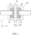
- FIG. 7 is a plan view schematically showing a simulation model
- FIGS. 8A to 8C are graphs showing the calculation result of the structural strain of a piezoelectric film
- FIG. 9A is a graph showing the relationship between the first width of a third electrode and the receiving sensitivity
- FIG. 9B is a graph showing the relationship between the first width of the third electrode and the electrostatic capacitance
- FIGS. 11A to 11C are plan views schematically showing simulation models
- FIGS. 12A to 12C are plan views schematically showing simulation models
- FIG. 13 is a graph showing a resonance frequency calculation result
- FIGS. 14A and 14B are graphs showing the receiving sensitivity and the electrostatic capacitance for each simulation model
- FIG. 15 is an enlarged partial plan view schematically showing the configuration of an ultrasonic device unit according to a second embodiment of the invention.
- FIG. 16 is an enlarged partial plan view schematically showing the configuration of an ultrasonic device unit according to a third embodiment Of the invention.
- FIG. 17 is an enlarged partial plan view schematically showing the configuration of an ultrasonic device unit according to a fourth embodiment of the invention.
- FIG. 1 schematically shows the configuration of a specific example of an electronic apparatus according to an embodiment of the invention, that is, the configuration of an ultrasonic diagnostic apparatus (ultrasonic imaging apparatus) 11 .
- the ultrasonic diagnostic apparatus 11 includes an apparatus body 12 and an ultrasonic probe (probe) 13 .
- the apparatus body 12 and the ultrasonic probe 13 are connected to each other by a cable 14 .
- the apparatus body 12 and the ultrasonic probe 13 perform transmission and reception of electrical signals therebetween through the cable 14 .
- a transmission circuit and a receiving circuit are provided in the apparatus body 12 .
- the transmission circuit transmits a driving signal toward the ultrasonic probe 13 .
- the receiving circuit receives a detection signal from the ultrasonic probe 13 .
- the ultrasonic probe 13 includes a housing 16 .
- the housing 16 includes a front side body 17 and a back side body 18 .
- the front side body 17 and the back side body 18 are coupled to each other.
- a cable port 19 is provided between the coupling surface of the front side body 17 and the coupling surface of the back side body 18 .
- the cable 14 is disposed in the cable port 19 .
- an ultrasonic device unit is supported by the housing 16 .
- the ultrasonic device unit transmits an ultrasonic wave in response to the reception of a driving signal, receives a reflected wave, and outputs a detection signal.
- a display device 23 is connected to the apparatus body 12 .
- a display panel 24 is built into the display device 23 .
- an image based on the ultrasonic wave detected by the ultrasonic probe 13 is displayed on the screen of the display panel 24 .
- An imaged detection result is displayed on the screen of the display panel 24 .
- an opening 25 is formed in the front side body 17 of the housing 16 .
- the opening 25 faces the housing space provided in the housing 16 .
- An ultrasonic device unit 26 is disposed in the housing space.
- the ultrasonic device unit 26 includes an acoustic matching layer 27 .
- the acoustic matching layer 27 is formed of, for example, silicone resin.
- the acoustic matching layer 27 has acoustic impedance (for example, 1.0 [MRayl] to 1.5 [MRayl]) close to the acoustic impedance 1.5 [MRayl] of the living body.
- the ultrasonic device unit 26 outputs an ultrasonic wave from the surface and receives a reflected wave of the ultrasonic wave.
- the ultrasonic diagnostic apparatus 11 or the ultrasonic probe 13 may have other structures.
- the ultrasonic probe 13 has an adhesive layer 28 .
- the adhesive layer 28 is, for example, laminated on the surface of the front side body 17 .
- the adhesive layer 28 has adhesion to an object, such as the skin.
- the ultrasonic probe 13 can be attached to the object due to the adhesive layer 28 . If the ultrasonic probe 13 is attached in this manner, the acoustic matching layer 27 is in close contact with the object.
- FIG. 3 conceptually shows the configuration of the ultrasonic device unit 26 according to the embodiment.
- the ultrasonic device unit 26 includes an element array (piezoelectric device group) 31 .
- the element array 31 includes ultrasonic transducers 32 that are disposed in an array.
- the ultrasonic transducer 32 is expressed per square mass.
- the ultrasonic transducers 32 of N rows and L columns are arranged in the element array 31 .
- one ultrasonic transducer 32 includes a transmission unit and a receiving unit.
- the transmission unit transmits an ultrasonic wave having a frequency determined according to the supply of an electrical signal.
- the receiving unit receives the ultrasonic wave having a determined frequency, and converts the ultrasonic wave into an electrical signal.
- FIG. 4 shows the structure of the ultrasonic device unit 26 according to a first embodiment of the invention in more detail.
- the ultrasonic device unit 26 includes a base 33 .
- a transmission unit 34 and a receiving unit 35 are formed on the base 33 .
- the ultrasonic device unit 26 is formed as one ultrasonic transducer element chip.
- the transmission unit 34 includes a plurality of first piezoelectric devices 36 .
- Each of the first piezoelectric devices 36 includes a vibrating film 37 .
- the details of the vibrating film 37 will be described later.
- the shape of the vibrating film 37 is drawn with a dotted line in a plan view from a direction perpendicular to the surface of the vibrating film 37 (in plan view from the thickness direction of the substrate).
- a piezoelectric element 38 is formed on the vibrating film 37 .
- a piezoelectric film 42 is interposed between an upper electrode 39 and a lower electrode 41 , as will be described later. These are superimposed in order.
- a plurality of first signal electrode lines 45 are formed on the surface of the base 33 .
- the first signal electrode lines 45 extend in the column direction (slice direction) of the array in parallel to each other.
- One first signal electrode line 45 is provided for each ultrasonic transducer element 32 .
- the first signal electrode line 45 forms the lower electrode 41 in each of the first piezoelectric devices 36 .
- a laminated film of titanium (Ti), iridium (Ir), platinum (Pt), and titanium (Ti) can be used.
- other conductive materials may be used for the first signal electrode line 45 .
- First common electrode lines 46 extending in the row direction (scanning direction) of the array are formed on the surface of the base 33 .
- the first common electrode lines 46 extend in the row direction of the array in parallel to each other. In all of the ultrasonic transducer 32 , the first common electrode lines 46 can be combined into one.
- the first common electrode line 46 forms the upper electrode 39 in each of the first piezoelectric devices 36 .
- the first common electrode line 46 can be formed of, for example, iridium (Ir). However, other conductive materials may be used for the first common electrode line 46 .
- the supply of power to the first piezoelectric device 36 is switched for each ultrasonic transducer 32 . Since the first piezoelectric devices 36 in each ultrasonic transducer 32 output ultrasonic waves at the same time, the number of first piezoelectric devices 36 in each ultrasonic transducer 32 can be determined according to the output level of the ultrasonic wave.
- the receiving unit 35 includes a plurality of second piezoelectric devices 47 .
- Each of the second piezoelectric devices 47 includes a vibrating film 48 .
- the details of the vibrating film 48 will be described later.
- FIG. 4 the shape of the vibrating film 48 is drawn with a dotted line in a plan view from a direction perpendicular to the surface of the vibrating film 48 (in plan view from the thickness direction of the substrate).
- a piezoelectric element 49 according to the present embodiment is formed on the vibrating film 48 .
- a first electrode 52 , a second electrode 53 , and a third electrode 54 are formed on a piezoelectric film 51 , as will be described more fully below. As shown in FIG.
- end portions 52 a and 53 a of the first and second electrodes 52 and 53 are defined in parallel to side portions 54 b and 54 b of the third electrode 54 .
- the end portions 52 a and 53 a and the side portions 54 b and 54 b may face each other, for example.
- the vibrating film 48 has a rectangular shape in a plan view (when viewed from a direction perpendicular to the surface of the vibrating film 48 ).
- the piezoelectric film 51 has a rectangular shape located on the inner side of the shape of the vibrating film 48 in a plan view.
- the center Cp of the piezoelectric film 51 overlaps the center Cv of the vibrating film 48 . Accordingly, in the piezoelectric film 51 , strain occurs in an in-plane direction in a region including the center Cv of the vibrating film 48 .
- a square may be applied.
- the shapes of the vibrating film 48 and the piezoelectric film 51 may not only be the rectangles but also polygons or ellipses.
- the third electrode 54 is formed in a band shape passing through the center Cv of the vibrating film 48 in plan view.
- the first and second electrodes 52 and 53 are separated from the third electrode 54 in a direction along the short sides of the vibrating film 48 .
- the third electrode 54 has a first width W 1 in parallel to the short side of the piezoelectric film 51 , and the first and second electrodes 52 and 53 are separated from the third electrode 54 in parallel to the short side of the piezoelectric film 51 with a second width W 2 equal to or greater than the first width W 1 .
- the first and second electrodes 52 and 53 are separated from the short sides of the vibrating film 48 , and are disposed between the short sides.
- each second piezoelectric device 47 is formed symmetrically with respect to a reference line BL parallel to the long sides of the vibrating film 48 . Also in a case where the vibrating film 48 and the piezoelectric film 51 do not have rectangular shapes, each second piezoelectric device 47 is formed symmetrically with respect to the reference line BL passing through the center Cp.
- a plurality of second signal electrode lines 56 are formed on the surface of the base 33 .
- the second signal electrode lines 56 extend in the column direction (slice direction) of the array in parallel to each other.
- One second signal electrode line 56 is provided for each ultrasonic transducer element 32 .
- the second signal electrode line 56 forms the third electrode 54 in each of the second piezoelectric devices 47 .
- iridium (Ir) can be used for the second signal electrode line 56 .
- other conductive materials may be used for the second signal electrode line 56 .
- Second common electrode lines (conductors) 57 extending in the column direction of the array in parallel to each other are formed on the surface of the base 33 .
- One second common electrode line 57 is provided for each ultrasonic transducer element 32 .
- the second common electrode line 57 is connected to the first and second electrodes 52 and 53 . Accordingly, the first and second electrodes 52 and 53 are short-circuited to each other at a position away from the piezoelectric film 51 .
- the second common electrode line 57 can be formed of, for example, iridium (Ir). However, other conductive materials may be used for the second common electrode line 57 .
- FIG. 5 shows the details of the transmission unit 34 .
- the base 33 includes a substrate 61 and a flexible film 62 .
- the flexible film 62 is formed on the entire surface of the substrate 61 .
- an opening 63 is formed in each first piezoelectric device 36 .
- the openings 63 are disposed in the form of an array for the substrate 61 .
- a partition wall 64 is provided between two adjacent openings 63 .
- the adjacent openings 63 are partitioned by the partition wall 64 .
- the flexible film 62 is formed by a silicon oxide (SiO 2 ) layer 65 laminated on the surface of the substrate 61 and a zirconium oxide (ZrO 2 ) layer 66 laminated on the surface of the silicon oxide layer 65 .
- the flexible film 62 is in contact with each opening 63 . In this manner, a part of the flexible film 62 forms the vibrating film 37 corresponding to the shape of the opening 63 .
- the first signal electrode line 45 , the piezoelectric film 42 , and the first common electrode line 46 are laminated in order on the surface of the vibrating film 37 .
- the piezoelectric film 42 can be formed of, for example, lead zirconate titanate (PZT). Other piezoelectric materials may be used for the piezoelectric film 42 .
- the piezoelectric film 42 completely covers the surface of the first signal electrode line 45 under the first common electrode line 46 . A short circuit between the first signal electrode line 45 and the first common electrode line 46 can be avoided due to the piezoelectric film 42 .
- the acoustic matching layer 27 covers the element array 31 .
- the acoustic matching layer 27 is laminated on the surface of the base 33 .
- a reinforcing plate 67 as a backing material is bonded to the back surface of the base 33 .
- the reinforcing plate 67 is formed in a flat plate shape.
- the back surface of the base 33 overlaps the surface of the reinforcing plate 67 .
- the surface of the reinforcing plate 67 is bonded to the back surface of the base 33 . In such bonding, the reinforcing plate 67 may be bonded to the base 33 with an adhesive.
- the reinforcing plate 67 increases the rigidity of the base 33 .
- the reinforcing plate 67 can include a rigid base, for example.
- Such a base may be formed of a metal material, such as a 42 alloy (iron-nickel alloy).
- FIG. 6 shows the details of the receiving unit 35 .
- an opening 68 is formed in each second piezoelectric device 47 .
- a part of the flexible film 62 forms the vibrating film 48 .
- a first surface 51 a of the piezoelectric film 51 is in contact with the vibrating film 48 .
- the first electrode 52 , the second electrode 53 , and the third electrode 54 are laminated on a second surface 51 b on the opposite side (back side) to the first surface 51 a .
- the piezoelectric film 51 can be formed of, for example, lead zirconate titanate (PZT). Other piezoelectric materials may be used for the piezoelectric film 42 .
- a material here, a zirconium oxide layer 66
- a conductor is disposed on the vibrating film 48 between the first electrode 52 , the second electrode 53 , and the third electrode 54 in a plan view.
- a driving signal is transmitted to the ultrasonic probe 13 from the apparatus body 12 .
- a pulse signal is supplied to the first piezoelectric device 36 .
- the pulse signal is supplied to the piezoelectric element 38 through the first signal electrode line 45 and the first common electrode line 46 .
- an electric field is applied to the piezoelectric film 42 between the upper electrode 39 and the lower electrode 41 .
- the piezoelectric film 42 vibrates at a frequency of an ultrasonic wave.
- the vibration of the piezoelectric film 42 is transmitted to the vibrating film 37 . Accordingly, the vibrating film 37 performs ultrasonic vibration.
- a desired ultrasonic beam is emitted toward a subject (for example, the inside of a human body).
- an ultrasonic wave is applied to each second piezoelectric device 47 .
- the reflected wave of the ultrasonic wave vibrates the vibrating film 48 .
- Ultrasonic vibration of the vibrating film 48 causes the piezoelectric film 51 to perform ultrasonic vibration at a desired frequency. If the vibrating film 48 performs ultrasonic vibration, the piezoelectric film 51 is strained according to the deformation of the vibrating film 48 . Surface charges are generated according to the strain ⁇ of the piezoelectric film 51 .
- An electric potential is detected between the short-circuited first and second electrodes 52 and 53 and the third electrode 54 . The electric potential is output as a detection signal from the second signal electrode line 56 and the second common electrode line 57 .
- the receiving circuit generates an ultrasonic image based on the detection signal. In such generation of an ultrasonic image, transmission and reception of ultrasonic waves are repeated. A linear scan or a sector scan is realized. An image signal is transmitted to the display device 23 from the receiving circuit. Based on the image signal, an ultrasonic image is displayed on the screen of the display panel 24 .
- an electrostatic capacitance is formed between the end portion 52 a of the first electrode 52 and the side portion 54 b of the third electrode 54 , and an electrostatic capacitance is formed between the end portion 53 a of the second electrode 53 and the side portion 54 b of the third electrode 54 .
- the electrostatic capacitance increases with an increase in the area of opposite surfaces. Accordingly, since the influence of the stray capacitance of the receiving circuit on the signal voltage detected between the first and third electrodes 52 and 54 and between the second and third electrodes 53 and 54 is reduced, a signal voltage that is measured is increased.
- the third electrode 54 is formed in a band shape passing through the center Cv of the vibrating film 48 in a plan view.
- the center Cv is separated from the edge of the opening 63 that is a boundary for a region where the vibrating film 48 is fixed to the substrate 61 . Therefore, at the center Cv, the strain ⁇ indicates a value close to the maximum value. In this manner, the signal voltage detected between the first and third electrodes 52 and 54 and between the second and third electrodes 53 and 54 can be maximized.
- the piezoelectric film 51 strain occurs in an in-plane direction in a region including the center Cv of the vibrating film 48 .
- the strain ⁇ indicates a value close to the maximum value. Therefore, since the piezoelectric film 51 on the center Cv can be strained to the maximum extent, the signal voltage detected between the first and third electrodes 52 and 54 and between the second and third electrodes 53 and 54 can be maximized.
- the center Cp of the piezoelectric film 51 overlaps the center Cv of the vibrating film 48 . Since the piezoelectric film 51 is also easily strained at the same center Cv as the vibrating film 48 , the strain ⁇ of the vibrating film 48 can be maximized.
- the piezoelectric film 51 is located on the inside rather than corresponding to the shape of the vibrating film 48 in a plan view.
- the vibrating film 48 and the piezoelectric film 51 have a rectangular shape in a plan view. In a rectangle, the sides are perpendicular to each other. Accordingly, since patterning becomes easy, it is possible to increase the arrangement density.
- the first and second electrodes 52 and 53 are separated from the third electrode 54 in a direction along the short sides of the vibrating film 48 . If the electrodes 52 and 53 are separated from the third electrode 54 in the direction along the short sides of the vibrating film 48 , the strain of the piezoelectric film 51 occurring in the direction of the short sides is maximized. Therefore, the signal voltage can be maximized.
- the strain ⁇ of the vibrating film 48 can be maximized.
- the second piezoelectric device 47 is formed symmetrically with respect to the reference line BL in parallel to the long sides of the vibrating film 48 , the strain ⁇ of the vibrating film 48 can be maximized in the reference line BL.
- the third electrode 54 is provided so as to overlap the reference line BL. That is, the second piezoelectric device 47 is formed line-symmetrically with respect to the third electrode 54 .
- a material other than a conductor may be disposed on the vibrating film 48 between the first electrode 52 , the second electrode 53 , and the third electrode 54 in a plan view. If a conductor is disposed here, a voltage path is diverted toward the conductor. Accordingly, it is not possible to increase the signal voltage that is measured. For example, if a material other than a conductor, such as an insulator, is disposed, it is possible to reliably increase the signal voltage.
- the present inventors calculated the strain of the piezoelectric film 51 . As shown in FIG. 7 , in such calculation, a simulation model SM of the second piezoelectric device 47 was constructed. The shapes of the vibrating film 48 and the piezoelectric film 51 were set to be squares.
- Simulation was performed using a finite element method for realizing the piezoelectric effect.
- the length of the short side of the shape of the vibrating film 48 was 40 ⁇ m, and the length of the short side of the piezoelectric film 51 was 32 ⁇ m.
- the vibrating film 48 includes SiO 2 (1000 nm), ZrO 2 (400 nm), and PZT (1350 nm) in order from the bottom.
- the thickness of each of the first, second, and third electrodes 52 , 53 , and 54 was 50 nm.
- a data set of PZT-5H was adopted as the piezoelectric tensor and the stiffness tensor of PZT used in the simulation.
- the principal axis of the tensor was set to a direction perpendicular to the reference line BL (direction in which an initialization electric field was applied).
- the Young's moduli of SiO 2 and ZrO 2 were 75 GPa and 190 GPa, respectively.
- the Young's moduli of the first, second, and third electrodes 52 , 53 , and 54 were 200 GPa. 1 atmosphere was applied to the vibrating film 48 from above, and the strain at that time was examined.
- the first width W 1 of the third electrode 54 was set to 5 [ ⁇ m].
- x, y, and z axes were set in the simulation model SM. Since the second piezoelectric device 47 is formed symmetrically with respect to the reference line BL, an x-axis direction strain ⁇ x, a y-axis direction strain ⁇ y, and a z-axis direction strain ⁇ z were calculated for each x-axis direction position on one side of the reference line BL.
- the x axis is perpendicular to the reference line BL, and the y axis is parallel to the reference line BL.
- the value of the z-axis direction strain ⁇ z was the maximum immediately below the third electrode 54 , and was 46 ⁇ 10 ⁇ 6 .
- absolute values of the x-axis direction strain ⁇ x and the y-axis direction strain ⁇ y were the maximum immediately below the third electrode 54 , and were ⁇ 64 ⁇ 10 ⁇ 6 and ⁇ 75 ⁇ 10 ⁇ 7 , respectively.
- the x-axis direction strain ⁇ x is about 10 times larger than the y-axis direction strain ⁇ y. That is, in the invention, a direction in which the strain is the maximum (x-axis direction) and the reference line BL are perpendicular to each other. When such an electrode arrangement is adopted, the receiving sensitivity is maximized.
- the groove 55 is formed between the first and third electrodes 52 and 54 and between the second and third electrodes 53 and 54 .
- the groove 55 acts advantageously when increasing the receiving sensitivity. This is because the strain of the piezoelectric film 51 due to sound pressure is concentrated on the groove 55 as the depth of the groove 55 increases. If the thickness of the piezoelectric film 51 reduced by the groove 55 is 2 ⁇ 3 or less of the original thickness, an increase in the receiving sensitivity of 20% or more is observed.
- the piezoelectric film 51 may be subjected to polarization processing.
- polarization processing is performed by an electric field vector from the first electrode 52 to the third electrode 54
- polarization processing is performed by an electric field vector from the second electrode 53 to the third electrode 54 .
- an electric field for the polarization processing of the piezoelectric body is applied in a direction of the strain ⁇ showing the maximum value (axis of symmetry of the short sides of the vibrating film).
- the present inventors examined the influence of the first width W 1 of the third electrode.
- the receiving sensitivity and the electrostatic capacitance were calculated in the simulation model SM of the second piezoelectric device 47 .
- the first width W 1 of the third electrode 54 was changed.
- FIGS. 9A and 9B it was confirmed that the receiving sensitivity was increased if the first width W 1 of the third electrode 54 was reduced. It was confirmed that the electrostatic capacitance was maintained even if the first width W 1 was reduced.
- the receiving sensitivity and the electrostatic capacitance were calculated in the simulation model SM of the second piezoelectric device 47 .
- the first width W 1 of the third electrode 54 was fixed to 5 [ ⁇ m]. As a result, as shown in FIGS.
- the first and second electrodes 52 and 53 are separated from the third electrode 54 in parallel to the short side of the piezoelectric film 51 with the second width W 2 equal to or greater than the first width W 1 . Therefore, since the electrostatic capacitance C is reduced, it is possible to increase the receiving sensitivity.
- the present inventors examined the advantages of the second piezoelectric device 47 .
- a simulation model SM 1 of a comparative example FIG. 11A
- a simulation model SM 2 of the second piezoelectric device 47 FIG. 11B
- a simulation model SM 3 according to another embodiment FIG. 11C
- the third electrode 54 was omitted from the second piezoelectric device 47 .
- the end portion 53 a of the second electrode 53 was made to face the end portion 53 a of the first electrode 52 .
- the third electrode 54 having a band shape was disposed along a diagonal line Di.
- the first electrode 52 was made to face the third electrode 54 over the entire length of a contour 71 on the piezoelectric film 51 .
- the second electrode 53 was made to face the third electrode 54 over the entire length of a contour 72 on the piezoelectric film 51 .
- the distance W 2 between electrodes was set to 5 [ ⁇ m] for all electrodes.
- the receiving sensitivity and the electrostatic capacitance were calculated in the simulation models SM 1 , SM 2 , and SM 3 .
- the simulation models SM 1 , SM 2 , and SM 3 are calculated based on the following dimensions.
- the length of the short side of the contour of the vibrating film was 40 ⁇ m, and the length of the short side of the piezoelectric film 51 was 32 ⁇ m.
- the vibrating film includes SiO 2 (1000 nm), ZrO 2 (400 nm), and PZT (1350 nm) in order from below.
- the thickness of each of the first, second, and third electrodes 52 , 53 , and 54 was 50 nm.
- a data set of PZT-5H was adopted as the piezoelectric tensor and the stiffness tensor of PZT used in the simulation.
- the principal axis of the tensor was set to a direction perpendicular to the reference line BL (direction in which an initialization electric field was applied).
- the Young's moduli of SiO 2 and ZrO 2 were 75 GPa and 190 GPa, respectively.
- the Young's moduli of the first, second, and third electrodes 52 , 53 , and 54 were 200 GPa. Simulation was performed using a finite element method for realizing the piezoelectric effect.
- the present inventors further constructed a simulation model in examining the advantages.
- the aspect ratio of each of the vibrating film 48 and the piezoelectric film 51 was changed in simulation models SM 4 , SM 5 , and SM 6 .
- the vibrating film 48 and the piezoelectric film 51 were formed in rectangular shapes, and the aspect ratio was set to 2. That is, the length of the long side was set to twice the length of the short side.
- the distance between electrodes was set to 5 [ ⁇ m] for all electrodes.
- the receiving sensitivity and the electrostatic capacitance were similarly calculated in the simulation models SM 4 , SM 5 , and SM 6 .
- the resonance frequency of the vibrating film depends on other dimensions of the vibrating film
- the resonance frequency of the simulation models SM 1 to SM 6 was changed in a range of 8.5 MHz to 8.8 MHz according to the setting of the dimensions as shown in FIG. 13 .
- FIG. 14A it was confirmed that the high receiving sensitivity was obtained in the simulation models SM 1 and SM 4 .
- the simulation model SM 3 and SM 6 it was observed that the receiving sensitivity was halved compared with the simulation models SM 1 and SM 4 .
- the simulation models SM 2 and SM 5 it was confirmed that the receiving sensitivity was reduced compared with the simulation models SM 1 and SM 4 but relatively high receiving sensitivity was secured.
- the receiving sensitivity was improved in the simulation models SM 4 to SM 6 of the rectangular shape having an aspect ratio of 2 rather than the square simulation models SM 1 to SM 3 .
- the first, second, and third electrodes 52 , 53 , and 54 are provided in parallel to the reference line BL, it is possible to obtain the maximum receiving sensitivity by setting the reference line BL in parallel to the long side direction. In other words, it is possible to obtain the maximum receiving sensitivity by providing the first, second, and third electrodes 52 , 53 , and 54 in parallel to the short side direction.
- the short side and the long side of a vibrating film were set to 32.5 ⁇ m and 65 ⁇ m, respectively.
- One atmosphere was applied perpendicular to the vibrating film surface.
- the thickness of SiO 2 was set to 1000 nm
- the thickness of ZrO 2 was set to 400 nm
- the thickness of PZT was set to 1350 nm
- the thickness of an electrode was set to 50 nm.
- the first, second, and third electrodes 52 , 53 , and 54 are provided in parallel to the reference line BL, but it is possible to obtain the maximum receiving sensitivity by setting the reference line BL in parallel to the long side direction. In other words, it is possible to obtain the maximum receiving sensitivity by providing the first, second, and third electrodes 52 , 53 , and 54 in parallel to the short side direction.
- FIG. 15 schematically shows the structure of an ultrasonic device unit 26 a according to a second embodiment of the invention.
- second piezoelectric devices 47 are arranged in a slice direction in the receiving unit 35 .
- a second signal electrode line (conductor) 56 a forms a third electrode 54 in common with the plurality of second piezoelectric devices 47 .
- the third electrode 54 traverses the surface of the corresponding piezoelectric film 51 .
- a second common electrode line 57 a forms a first electrode 52 in common with the plurality of second piezoelectric devices 47 arranged in the slice direction.
- the second common electrode line 57 a forms a second electrode 53 in common with the plurality of second piezoelectric devices 47 arranged in the slice direction.
- Other structures are the same as the ultrasonic device unit 26 of the first embodiment described above.
- FIG. 16 schematically shows the structure of an ultrasonic device unit 26 b according to a third embodiment of the invention.
- second piezoelectric devices 47 are arranged in a scanning direction and a slice direction in the receiving unit 35 .
- a second signal electrode line (conductor) 56 a forms a third electrode 54 in common with the plurality of second piezoelectric devices 47 .
- the second signal electrode lines 56 a extend in the slice direction in parallel to each other.
- the third electrode 54 traverses the surface of the corresponding piezoelectric film 51 .
- a second common electrode line 57 a forms first and second electrodes 52 and 53 in common with the plurality of second piezoelectric devices 47 arranged in the slice direction.
- a second common electrode line 57 a forms first and second electrodes 52 and 53 in common with a pair of second piezoelectric devices 47 arranged in the scanning direction.
- the second common electrode lines 57 a are connected to each other.
- Other structures are the same as the ultrasonic device units 26 and 26 a of the first or second embodiment described above.
- FIG. 17 schematically shows the structure of an ultrasonic device unit 26 c according to a fourth embodiment of the invention.
- the second piezoelectric device 47 a is formed similar to the simulation model SM 3 described above.
- the second piezoelectric devices 47 a are arranged in a slice direction.
- a second signal electrode line (conductor) 56 a forms a third electrode 54 in common with a plurality of second piezoelectric devices 47 a .
- the third electrode 54 traverses the surface of the corresponding piezoelectric film 51 .
- a second common electrode line 57 a forms a first electrode 52 in common with the plurality of second piezoelectric devices 47 a arranged in the slice direction.
- the second common electrode line 57 a forms a second electrode 53 in common with the plurality of second piezoelectric devices 47 a arranged in the slice direction.
- Other structures are the same as the ultrasonic device unit 26 of the first embodiment described above.
Landscapes
- Health & Medical Sciences (AREA)
- Life Sciences & Earth Sciences (AREA)
- Engineering & Computer Science (AREA)
- Physics & Mathematics (AREA)
- Heart & Thoracic Surgery (AREA)
- Surgery (AREA)
- Nuclear Medicine, Radiotherapy & Molecular Imaging (AREA)
- Pathology (AREA)
- Radiology & Medical Imaging (AREA)
- Biomedical Technology (AREA)
- Veterinary Medicine (AREA)
- Medical Informatics (AREA)
- Molecular Biology (AREA)
- Biophysics (AREA)
- Animal Behavior & Ethology (AREA)
- General Health & Medical Sciences (AREA)
- Public Health (AREA)
- Mechanical Engineering (AREA)
- Gynecology & Obstetrics (AREA)
- Acoustics & Sound (AREA)
- Ultra Sonic Daignosis Equipment (AREA)
- Transducers For Ultrasonic Waves (AREA)
Abstract
Description
Claims (11)
Applications Claiming Priority (2)
| Application Number | Priority Date | Filing Date | Title |
|---|---|---|---|
| JP2015108929A JP6613628B2 (en) | 2015-05-28 | 2015-05-28 | Piezoelectric device and probe, electronic apparatus and ultrasonic imaging apparatus |
| JP2015-108929 | 2015-05-28 |
Publications (2)
| Publication Number | Publication Date |
|---|---|
| US20160345932A1 US20160345932A1 (en) | 2016-12-01 |
| US10603009B2 true US10603009B2 (en) | 2020-03-31 |
Family
ID=56096484
Family Applications (1)
| Application Number | Title | Priority Date | Filing Date |
|---|---|---|---|
| US15/167,920 Active 2038-05-29 US10603009B2 (en) | 2015-05-28 | 2016-05-27 | Piezoelectric device, probe, electronic apparatus, and ultrasonic imaging apparatus |
Country Status (4)
| Country | Link |
|---|---|
| US (1) | US10603009B2 (en) |
| EP (1) | EP3097987B1 (en) |
| JP (1) | JP6613628B2 (en) |
| CN (1) | CN106175827B (en) |
Families Citing this family (8)
| Publication number | Priority date | Publication date | Assignee | Title |
|---|---|---|---|---|
| CN106416297B (en) * | 2014-06-30 | 2019-03-22 | 精工爱普生株式会社 | Ultrasonic sensor and method of making the same |
| JP2018164039A (en) * | 2017-03-27 | 2018-10-18 | セイコーエプソン株式会社 | Piezoelectric element, piezoelectric device, ultrasonic probe, and electronic apparatus |
| CN108433744B (en) * | 2018-04-23 | 2023-11-28 | 中国科学院苏州生物医学工程技术研究所 | Ultrasonic transducer, ultrasonic probe and ultrasonic hydrophone |
| KR102683225B1 (en) * | 2018-12-05 | 2024-07-08 | 엘지디스플레이 주식회사 | Display apparatus |
| CN111136001B (en) * | 2020-01-16 | 2024-12-03 | 重庆大学 | Mechanical slot enhanced differential piezoelectric ultrasonic transducer and working method thereof |
| CN116326254A (en) * | 2020-09-28 | 2023-06-23 | 斯派克塔震动科技与声学德累斯顿有限公司 | Exciter element |
| JP7627110B2 (en) * | 2020-12-01 | 2025-02-05 | Tdk株式会社 | Piezoelectric transducers and ultrasonic transducers |
| CN120306233B (en) * | 2025-06-17 | 2025-08-26 | 中国工程物理研究院电子工程研究所 | Dual-electrode piezoelectric film ultrasonic transducer and array coupling method thereof |
Citations (9)
| Publication number | Priority date | Publication date | Assignee | Title |
|---|---|---|---|---|
| US5823962A (en) * | 1996-09-02 | 1998-10-20 | Siemens Aktiengesellschaft | Ultrasound transducer for diagnostic and therapeutic use |
| US20020105250A1 (en) | 2001-01-24 | 2002-08-08 | U.S. Philips Corporation | Array of ultrasound transducers |
| US20030137224A1 (en) | 2002-01-18 | 2003-07-24 | Pegasus Technologies Ltd. | Cylindrical ultrasound transceivers |
| JP2005039720A (en) | 2003-07-18 | 2005-02-10 | Osaka Industrial Promotion Organization | Piezoelectric ultrasonic sensor element |
| CN101192644A (en) | 2006-11-30 | 2008-06-04 | 中国科学院声学研究所 | A sensing diaphragm comprising piezoelectric films with two polarization directions |
| US20090001853A1 (en) * | 2006-03-03 | 2009-01-01 | Olympus Medical Systems Corp. | Ultrasound transducer manufactured by using micromachining process, its device, endoscopic ultrasound diagnosis system thereof, and method for controlling the same |
| US8299550B2 (en) * | 2009-04-10 | 2012-10-30 | Canon Kabushiki Kaisha | Electromechanical transducer |
| JP2013098724A (en) | 2011-10-31 | 2013-05-20 | Konica Minolta Holdings Inc | Piezoelectric device, ultrasonic probe and manufacturing method of piezoelectric device |
| US20150273526A1 (en) | 2014-03-27 | 2015-10-01 | Seiko Epson Corporation | Piezoelectric element, piezoelectric device, probe, electronic machine, and ultrasonic image apparatus |
Family Cites Families (4)
| Publication number | Priority date | Publication date | Assignee | Title |
|---|---|---|---|---|
| JPS5842968A (en) * | 1981-09-07 | 1983-03-12 | Hitachi Ltd | Ultrasonic probe |
| JP5486689B2 (en) * | 2010-10-15 | 2014-05-07 | 株式会社日立メディコ | Ultrasonic transducer and ultrasonic diagnostic apparatus using the same |
| JP6078994B2 (en) * | 2012-06-13 | 2017-02-15 | セイコーエプソン株式会社 | Ultrasonic transducer element unit, probe, probe head, electronic device, and ultrasonic diagnostic apparatus |
| JP6252279B2 (en) * | 2013-03-29 | 2017-12-27 | セイコーエプソン株式会社 | ULTRASONIC TRANSDUCER DEVICE AND PROBE, ELECTRONIC DEVICE, AND ULTRASONIC IMAGING DEVICE |
-
2015
- 2015-05-28 JP JP2015108929A patent/JP6613628B2/en active Active
-
2016
- 2016-05-25 EP EP16171288.0A patent/EP3097987B1/en active Active
- 2016-05-26 CN CN201610361700.2A patent/CN106175827B/en active Active
- 2016-05-27 US US15/167,920 patent/US10603009B2/en active Active
Patent Citations (11)
| Publication number | Priority date | Publication date | Assignee | Title |
|---|---|---|---|---|
| US5823962A (en) * | 1996-09-02 | 1998-10-20 | Siemens Aktiengesellschaft | Ultrasound transducer for diagnostic and therapeutic use |
| US20020105250A1 (en) | 2001-01-24 | 2002-08-08 | U.S. Philips Corporation | Array of ultrasound transducers |
| JP2002271897A (en) | 2001-01-24 | 2002-09-20 | Koninkl Philips Electronics Nv | Array of ultrasonic transducers |
| US20030137224A1 (en) | 2002-01-18 | 2003-07-24 | Pegasus Technologies Ltd. | Cylindrical ultrasound transceivers |
| JP2005039720A (en) | 2003-07-18 | 2005-02-10 | Osaka Industrial Promotion Organization | Piezoelectric ultrasonic sensor element |
| US20090001853A1 (en) * | 2006-03-03 | 2009-01-01 | Olympus Medical Systems Corp. | Ultrasound transducer manufactured by using micromachining process, its device, endoscopic ultrasound diagnosis system thereof, and method for controlling the same |
| CN101192644A (en) | 2006-11-30 | 2008-06-04 | 中国科学院声学研究所 | A sensing diaphragm comprising piezoelectric films with two polarization directions |
| US8299550B2 (en) * | 2009-04-10 | 2012-10-30 | Canon Kabushiki Kaisha | Electromechanical transducer |
| JP2013098724A (en) | 2011-10-31 | 2013-05-20 | Konica Minolta Holdings Inc | Piezoelectric device, ultrasonic probe and manufacturing method of piezoelectric device |
| US20150273526A1 (en) | 2014-03-27 | 2015-10-01 | Seiko Epson Corporation | Piezoelectric element, piezoelectric device, probe, electronic machine, and ultrasonic image apparatus |
| JP2015195351A (en) | 2014-03-27 | 2015-11-05 | セイコーエプソン株式会社 | Piezoelectric element, piezoelectric device and probe, electronic apparatus and ultrasonic imaging apparatus |
Non-Patent Citations (1)
| Title |
|---|
| Extended European Search Report dated Oct. 18, 2016 as received in Application No. 16171288.0. |
Also Published As
| Publication number | Publication date |
|---|---|
| JP2016225750A (en) | 2016-12-28 |
| CN106175827A (en) | 2016-12-07 |
| EP3097987A1 (en) | 2016-11-30 |
| CN106175827B (en) | 2021-05-18 |
| US20160345932A1 (en) | 2016-12-01 |
| EP3097987B1 (en) | 2021-06-16 |
| JP6613628B2 (en) | 2019-12-04 |
Similar Documents
| Publication | Publication Date | Title |
|---|---|---|
| US10603009B2 (en) | Piezoelectric device, probe, electronic apparatus, and ultrasonic imaging apparatus | |
| JP6519212B2 (en) | Piezoelectric element, piezoelectric device and probe, electronic device and ultrasonic imaging apparatus | |
| US9184370B2 (en) | Ultrasonic transducer device, ultrasonic measurement apparatus, head unit, probe, and ultrasonic imaging apparatus | |
| TWI599237B (en) | Ultrasonic transducer element chip, probe, electronic instrument, and ultrasonic diagnostic device | |
| US9199277B2 (en) | Ultrasonic measurement device, ultrasonic head unit, ultrasonic probe, and ultrasonic image device | |
| CN105310721B (en) | Ultrasonic device, method of manufacturing the same, probe, and electronic apparatus | |
| JP6326833B2 (en) | Ultrasonic device, method for manufacturing ultrasonic device, probe, electronic device, ultrasonic imaging apparatus | |
| US10042044B2 (en) | Ultrasonic device, probe, electronic device, and ultrasonic imaging apparatus | |
| CN105559821B (en) | Ultrasonic probe, electronic device, and ultrasonic imaging apparatus | |
| JP6665667B2 (en) | Ultrasonic device, ultrasonic module, and ultrasonic measurement device | |
| US9246077B2 (en) | Ultrasonic transducer device, head unit, probe, and ultrasonic imaging apparatus | |
| US10363574B2 (en) | Piezoelectric element, probe, and ultrasonic measurement apparatus | |
| US9252352B2 (en) | Ultrasonic transducer device, head unit, probe, and ultrasonic imaging apparatus | |
| US20170040527A1 (en) | Piezoelectric element, probe, ultrasonic measurement device, electronic apparatus, polarization processing method, and initialization device | |
| JP2017029571A (en) | Piezoelectric device, probe, electronic apparatus, and ultrasound imaging apparatus |
Legal Events
| Date | Code | Title | Description |
|---|---|---|---|
| AS | Assignment |
Owner name: SEIKO EPSON CORPORATION, JAPAN Free format text: ASSIGNMENT OF ASSIGNORS INTEREST;ASSIGNORS:MIYAZAWA, HIROMU;YAMADA, MASAYOSHI;ITO, HIROSHI;AND OTHERS;SIGNING DATES FROM 20160610 TO 20160615;REEL/FRAME:038949/0399 |
|
| STPP | Information on status: patent application and granting procedure in general |
Free format text: NON FINAL ACTION MAILED |
|
| STPP | Information on status: patent application and granting procedure in general |
Free format text: RESPONSE TO NON-FINAL OFFICE ACTION ENTERED AND FORWARDED TO EXAMINER |
|
| STPP | Information on status: patent application and granting procedure in general |
Free format text: EX PARTE QUAYLE ACTION MAILED |
|
| STPP | Information on status: patent application and granting procedure in general |
Free format text: RESPONSE TO EX PARTE QUAYLE ACTION ENTERED AND FORWARDED TO EXAMINER |
|
| STPP | Information on status: patent application and granting procedure in general |
Free format text: NOTICE OF ALLOWANCE MAILED -- APPLICATION RECEIVED IN OFFICE OF PUBLICATIONS |
|
| STPP | Information on status: patent application and granting procedure in general |
Free format text: PUBLICATIONS -- ISSUE FEE PAYMENT RECEIVED |
|
| STPP | Information on status: patent application and granting procedure in general |
Free format text: PUBLICATIONS -- ISSUE FEE PAYMENT VERIFIED |
|
| STCF | Information on status: patent grant |
Free format text: PATENTED CASE |
|
| MAFP | Maintenance fee payment |
Free format text: PAYMENT OF MAINTENANCE FEE, 4TH YEAR, LARGE ENTITY (ORIGINAL EVENT CODE: M1551); ENTITY STATUS OF PATENT OWNER: LARGE ENTITY Year of fee payment: 4 |