US10591663B2 - Light guide plate unit, backlight unit comprising same, and liquid crystal display device - Google Patents
Light guide plate unit, backlight unit comprising same, and liquid crystal display device Download PDFInfo
- Publication number
- US10591663B2 US10591663B2 US16/082,485 US201716082485A US10591663B2 US 10591663 B2 US10591663 B2 US 10591663B2 US 201716082485 A US201716082485 A US 201716082485A US 10591663 B2 US10591663 B2 US 10591663B2
- Authority
- US
- United States
- Prior art keywords
- guide plate
- light guide
- adhesive layer
- bead
- plate unit
- Prior art date
- Legal status (The legal status is an assumption and is not a legal conclusion. Google has not performed a legal analysis and makes no representation as to the accuracy of the status listed.)
- Active
Links
- 239000004973 liquid crystal related substance Substances 0.000 title claims abstract description 28
- 239000012790 adhesive layer Substances 0.000 claims abstract description 60
- 239000011324 bead Substances 0.000 claims abstract description 43
- 229920005989 resin Polymers 0.000 claims description 34
- 239000011347 resin Substances 0.000 claims description 34
- GWEVSGVZZGPLCZ-UHFFFAOYSA-N Titan oxide Chemical compound O=[Ti]=O GWEVSGVZZGPLCZ-UHFFFAOYSA-N 0.000 claims description 24
- 239000011159 matrix material Substances 0.000 claims description 16
- 239000002245 particle Substances 0.000 claims description 14
- -1 acryl Chemical group 0.000 claims description 6
- 239000004793 Polystyrene Substances 0.000 claims description 5
- 238000000149 argon plasma sintering Methods 0.000 claims description 5
- 150000001875 compounds Chemical class 0.000 claims description 5
- VYPSYNLAJGMNEJ-UHFFFAOYSA-N Silicium dioxide Chemical compound O=[Si]=O VYPSYNLAJGMNEJ-UHFFFAOYSA-N 0.000 claims description 4
- 239000000203 mixture Substances 0.000 claims description 4
- 229920002223 polystyrene Polymers 0.000 claims description 4
- JOYRKODLDBILNP-UHFFFAOYSA-N Ethyl urethane Chemical compound CCOC(N)=O JOYRKODLDBILNP-UHFFFAOYSA-N 0.000 claims description 3
- XUIMIQQOPSSXEZ-UHFFFAOYSA-N Silicon Chemical compound [Si] XUIMIQQOPSSXEZ-UHFFFAOYSA-N 0.000 claims description 3
- 239000003822 epoxy resin Substances 0.000 claims description 3
- 229920000647 polyepoxide Polymers 0.000 claims description 3
- 229920001296 polysiloxane Polymers 0.000 claims description 3
- 229910052710 silicon Inorganic materials 0.000 claims description 3
- 239000010703 silicon Substances 0.000 claims description 3
- 229910052681 coesite Inorganic materials 0.000 claims description 2
- 229920001577 copolymer Polymers 0.000 claims description 2
- 229910052906 cristobalite Inorganic materials 0.000 claims description 2
- 239000000377 silicon dioxide Substances 0.000 claims description 2
- 229910052682 stishovite Inorganic materials 0.000 claims description 2
- 229910052905 tridymite Inorganic materials 0.000 claims description 2
- 229920003229 poly(methyl methacrylate) Polymers 0.000 claims 1
- 239000004926 polymethyl methacrylate Substances 0.000 claims 1
- 239000000853 adhesive Substances 0.000 description 30
- 230000001070 adhesive effect Effects 0.000 description 30
- 230000000694 effects Effects 0.000 description 20
- 230000000052 comparative effect Effects 0.000 description 12
- 239000004408 titanium dioxide Substances 0.000 description 11
- 238000010586 diagram Methods 0.000 description 9
- 238000000034 method Methods 0.000 description 9
- 230000003247 decreasing effect Effects 0.000 description 7
- 239000010410 layer Substances 0.000 description 5
- 239000002904 solvent Substances 0.000 description 4
- 239000003795 chemical substances by application Substances 0.000 description 3
- 239000003431 cross linking reagent Substances 0.000 description 3
- 239000000463 material Substances 0.000 description 3
- 238000005259 measurement Methods 0.000 description 3
- 229920001187 thermosetting polymer Polymers 0.000 description 3
- 238000009792 diffusion process Methods 0.000 description 2
- 238000002474 experimental method Methods 0.000 description 2
- 229920000139 polyethylene terephthalate Polymers 0.000 description 2
- 239000005020 polyethylene terephthalate Substances 0.000 description 2
- 238000007639 printing Methods 0.000 description 2
- 238000007650 screen-printing Methods 0.000 description 2
- BRPQOXSCLDDYGP-UHFFFAOYSA-N calcium oxide Chemical compound [O-2].[Ca+2] BRPQOXSCLDDYGP-UHFFFAOYSA-N 0.000 description 1
- 239000000292 calcium oxide Substances 0.000 description 1
- ODINCKMPIJJUCX-UHFFFAOYSA-N calcium oxide Inorganic materials [Ca]=O ODINCKMPIJJUCX-UHFFFAOYSA-N 0.000 description 1
- 239000000470 constituent Substances 0.000 description 1
- 238000001035 drying Methods 0.000 description 1
- 238000001704 evaporation Methods 0.000 description 1
- 230000008020 evaporation Effects 0.000 description 1
- 239000011521 glass Substances 0.000 description 1
- 238000007646 gravure printing Methods 0.000 description 1
- 239000003999 initiator Substances 0.000 description 1
- 238000007641 inkjet printing Methods 0.000 description 1
- 239000011256 inorganic filler Substances 0.000 description 1
- 229910003475 inorganic filler Inorganic materials 0.000 description 1
- 239000012948 isocyanate Substances 0.000 description 1
- 150000002513 isocyanates Chemical class 0.000 description 1
- 238000004519 manufacturing process Methods 0.000 description 1
- 239000011148 porous material Substances 0.000 description 1
Images

Classifications
-
- G—PHYSICS
- G02—OPTICS
- G02B—OPTICAL ELEMENTS, SYSTEMS OR APPARATUS
- G02B6/00—Light guides; Structural details of arrangements comprising light guides and other optical elements, e.g. couplings
- G02B6/0001—Light guides; Structural details of arrangements comprising light guides and other optical elements, e.g. couplings specially adapted for lighting devices or systems
- G02B6/0011—Light guides; Structural details of arrangements comprising light guides and other optical elements, e.g. couplings specially adapted for lighting devices or systems the light guides being planar or of plate-like form
- G02B6/0081—Mechanical or electrical aspects of the light guide and light source in the lighting device peculiar to the adaptation to planar light guides, e.g. concerning packaging
- G02B6/0086—Positioning aspects
- G02B6/0088—Positioning aspects of the light guide or other optical sheets in the package
-
- G—PHYSICS
- G02—OPTICS
- G02F—OPTICAL DEVICES OR ARRANGEMENTS FOR THE CONTROL OF LIGHT BY MODIFICATION OF THE OPTICAL PROPERTIES OF THE MEDIA OF THE ELEMENTS INVOLVED THEREIN; NON-LINEAR OPTICS; FREQUENCY-CHANGING OF LIGHT; OPTICAL LOGIC ELEMENTS; OPTICAL ANALOGUE/DIGITAL CONVERTERS
- G02F1/00—Devices or arrangements for the control of the intensity, colour, phase, polarisation or direction of light arriving from an independent light source, e.g. switching, gating or modulating; Non-linear optics
- G02F1/01—Devices or arrangements for the control of the intensity, colour, phase, polarisation or direction of light arriving from an independent light source, e.g. switching, gating or modulating; Non-linear optics for the control of the intensity, phase, polarisation or colour
- G02F1/13—Devices or arrangements for the control of the intensity, colour, phase, polarisation or direction of light arriving from an independent light source, e.g. switching, gating or modulating; Non-linear optics for the control of the intensity, phase, polarisation or colour based on liquid crystals, e.g. single liquid crystal display cells
- G02F1/133—Constructional arrangements; Operation of liquid crystal cells; Circuit arrangements
- G02F1/1333—Constructional arrangements; Manufacturing methods
- G02F1/1335—Structural association of cells with optical devices, e.g. polarisers or reflectors
- G02F1/133524—Light-guides, e.g. fibre-optic bundles, louvered or jalousie light-guides
-
- C—CHEMISTRY; METALLURGY
- C09—DYES; PAINTS; POLISHES; NATURAL RESINS; ADHESIVES; COMPOSITIONS NOT OTHERWISE PROVIDED FOR; APPLICATIONS OF MATERIALS NOT OTHERWISE PROVIDED FOR
- C09J—ADHESIVES; NON-MECHANICAL ASPECTS OF ADHESIVE PROCESSES IN GENERAL; ADHESIVE PROCESSES NOT PROVIDED FOR ELSEWHERE; USE OF MATERIALS AS ADHESIVES
- C09J11/00—Features of adhesives not provided for in group C09J9/00, e.g. additives
- C09J11/02—Non-macromolecular additives
- C09J11/04—Non-macromolecular additives inorganic
-
- C—CHEMISTRY; METALLURGY
- C09—DYES; PAINTS; POLISHES; NATURAL RESINS; ADHESIVES; COMPOSITIONS NOT OTHERWISE PROVIDED FOR; APPLICATIONS OF MATERIALS NOT OTHERWISE PROVIDED FOR
- C09J—ADHESIVES; NON-MECHANICAL ASPECTS OF ADHESIVE PROCESSES IN GENERAL; ADHESIVE PROCESSES NOT PROVIDED FOR ELSEWHERE; USE OF MATERIALS AS ADHESIVES
- C09J125/00—Adhesives based on homopolymers or copolymers of compounds having one or more unsaturated aliphatic radicals, each having only one carbon-to-carbon double bond, and at least one being terminated by an aromatic carbocyclic ring; Adhesives based on derivatives of such polymers
- C09J125/02—Homopolymers or copolymers of hydrocarbons
- C09J125/04—Homopolymers or copolymers of styrene
- C09J125/06—Polystyrene
-
- C—CHEMISTRY; METALLURGY
- C09—DYES; PAINTS; POLISHES; NATURAL RESINS; ADHESIVES; COMPOSITIONS NOT OTHERWISE PROVIDED FOR; APPLICATIONS OF MATERIALS NOT OTHERWISE PROVIDED FOR
- C09J—ADHESIVES; NON-MECHANICAL ASPECTS OF ADHESIVE PROCESSES IN GENERAL; ADHESIVE PROCESSES NOT PROVIDED FOR ELSEWHERE; USE OF MATERIALS AS ADHESIVES
- C09J133/00—Adhesives based on homopolymers or copolymers of compounds having one or more unsaturated aliphatic radicals, each having only one carbon-to-carbon double bond, and at least one being terminated by only one carboxyl radical, or of salts, anhydrides, esters, amides, imides, or nitriles thereof; Adhesives based on derivatives of such polymers
- C09J133/04—Homopolymers or copolymers of esters
- C09J133/06—Homopolymers or copolymers of esters of esters containing only carbon, hydrogen and oxygen, the oxygen atom being present only as part of the carboxyl radical
- C09J133/10—Homopolymers or copolymers of methacrylic acid esters
- C09J133/12—Homopolymers or copolymers of methyl methacrylate
-
- G—PHYSICS
- G02—OPTICS
- G02B—OPTICAL ELEMENTS, SYSTEMS OR APPARATUS
- G02B6/00—Light guides; Structural details of arrangements comprising light guides and other optical elements, e.g. couplings
- G02B6/0001—Light guides; Structural details of arrangements comprising light guides and other optical elements, e.g. couplings specially adapted for lighting devices or systems
- G02B6/0011—Light guides; Structural details of arrangements comprising light guides and other optical elements, e.g. couplings specially adapted for lighting devices or systems the light guides being planar or of plate-like form
- G02B6/0033—Means for improving the coupling-out of light from the light guide
- G02B6/0035—Means for improving the coupling-out of light from the light guide provided on the surface of the light guide or in the bulk of it
- G02B6/004—Scattering dots or dot-like elements, e.g. microbeads, scattering particles, nanoparticles
- G02B6/0043—Scattering dots or dot-like elements, e.g. microbeads, scattering particles, nanoparticles provided on the surface of the light guide
-
- G—PHYSICS
- G02—OPTICS
- G02B—OPTICAL ELEMENTS, SYSTEMS OR APPARATUS
- G02B6/00—Light guides; Structural details of arrangements comprising light guides and other optical elements, e.g. couplings
- G02B6/0001—Light guides; Structural details of arrangements comprising light guides and other optical elements, e.g. couplings specially adapted for lighting devices or systems
- G02B6/0011—Light guides; Structural details of arrangements comprising light guides and other optical elements, e.g. couplings specially adapted for lighting devices or systems the light guides being planar or of plate-like form
- G02B6/0033—Means for improving the coupling-out of light from the light guide
- G02B6/005—Means for improving the coupling-out of light from the light guide provided by one optical element, or plurality thereof, placed on the light output side of the light guide
- G02B6/0055—Reflecting element, sheet or layer
-
- G—PHYSICS
- G02—OPTICS
- G02B—OPTICAL ELEMENTS, SYSTEMS OR APPARATUS
- G02B6/00—Light guides; Structural details of arrangements comprising light guides and other optical elements, e.g. couplings
- G02B6/0001—Light guides; Structural details of arrangements comprising light guides and other optical elements, e.g. couplings specially adapted for lighting devices or systems
- G02B6/0011—Light guides; Structural details of arrangements comprising light guides and other optical elements, e.g. couplings specially adapted for lighting devices or systems the light guides being planar or of plate-like form
- G02B6/0033—Means for improving the coupling-out of light from the light guide
- G02B6/0058—Means for improving the coupling-out of light from the light guide varying in density, size, shape or depth along the light guide
- G02B6/0061—Means for improving the coupling-out of light from the light guide varying in density, size, shape or depth along the light guide to provide homogeneous light output intensity
-
- G—PHYSICS
- G02—OPTICS
- G02F—OPTICAL DEVICES OR ARRANGEMENTS FOR THE CONTROL OF LIGHT BY MODIFICATION OF THE OPTICAL PROPERTIES OF THE MEDIA OF THE ELEMENTS INVOLVED THEREIN; NON-LINEAR OPTICS; FREQUENCY-CHANGING OF LIGHT; OPTICAL LOGIC ELEMENTS; OPTICAL ANALOGUE/DIGITAL CONVERTERS
- G02F1/00—Devices or arrangements for the control of the intensity, colour, phase, polarisation or direction of light arriving from an independent light source, e.g. switching, gating or modulating; Non-linear optics
- G02F1/01—Devices or arrangements for the control of the intensity, colour, phase, polarisation or direction of light arriving from an independent light source, e.g. switching, gating or modulating; Non-linear optics for the control of the intensity, phase, polarisation or colour
- G02F1/13—Devices or arrangements for the control of the intensity, colour, phase, polarisation or direction of light arriving from an independent light source, e.g. switching, gating or modulating; Non-linear optics for the control of the intensity, phase, polarisation or colour based on liquid crystals, e.g. single liquid crystal display cells
- G02F1/133—Constructional arrangements; Operation of liquid crystal cells; Circuit arrangements
- G02F1/1333—Constructional arrangements; Manufacturing methods
- G02F1/1335—Structural association of cells with optical devices, e.g. polarisers or reflectors
- G02F1/133504—Diffusing, scattering, diffracting elements
-
- G—PHYSICS
- G02—OPTICS
- G02F—OPTICAL DEVICES OR ARRANGEMENTS FOR THE CONTROL OF LIGHT BY MODIFICATION OF THE OPTICAL PROPERTIES OF THE MEDIA OF THE ELEMENTS INVOLVED THEREIN; NON-LINEAR OPTICS; FREQUENCY-CHANGING OF LIGHT; OPTICAL LOGIC ELEMENTS; OPTICAL ANALOGUE/DIGITAL CONVERTERS
- G02F1/00—Devices or arrangements for the control of the intensity, colour, phase, polarisation or direction of light arriving from an independent light source, e.g. switching, gating or modulating; Non-linear optics
- G02F1/01—Devices or arrangements for the control of the intensity, colour, phase, polarisation or direction of light arriving from an independent light source, e.g. switching, gating or modulating; Non-linear optics for the control of the intensity, phase, polarisation or colour
- G02F1/13—Devices or arrangements for the control of the intensity, colour, phase, polarisation or direction of light arriving from an independent light source, e.g. switching, gating or modulating; Non-linear optics for the control of the intensity, phase, polarisation or colour based on liquid crystals, e.g. single liquid crystal display cells
- G02F1/133—Constructional arrangements; Operation of liquid crystal cells; Circuit arrangements
- G02F1/1333—Constructional arrangements; Manufacturing methods
- G02F1/1335—Structural association of cells with optical devices, e.g. polarisers or reflectors
- G02F1/1336—Illuminating devices
- G02F1/133615—Edge-illuminating devices, i.e. illuminating from the side
-
- G—PHYSICS
- G02—OPTICS
- G02B—OPTICAL ELEMENTS, SYSTEMS OR APPARATUS
- G02B6/00—Light guides; Structural details of arrangements comprising light guides and other optical elements, e.g. couplings
- G02B6/0001—Light guides; Structural details of arrangements comprising light guides and other optical elements, e.g. couplings specially adapted for lighting devices or systems
- G02B6/0011—Light guides; Structural details of arrangements comprising light guides and other optical elements, e.g. couplings specially adapted for lighting devices or systems the light guides being planar or of plate-like form
- G02B6/0065—Manufacturing aspects; Material aspects
-
- G—PHYSICS
- G02—OPTICS
- G02F—OPTICAL DEVICES OR ARRANGEMENTS FOR THE CONTROL OF LIGHT BY MODIFICATION OF THE OPTICAL PROPERTIES OF THE MEDIA OF THE ELEMENTS INVOLVED THEREIN; NON-LINEAR OPTICS; FREQUENCY-CHANGING OF LIGHT; OPTICAL LOGIC ELEMENTS; OPTICAL ANALOGUE/DIGITAL CONVERTERS
- G02F2201/00—Constructional arrangements not provided for in groups G02F1/00 - G02F7/00
- G02F2201/34—Constructional arrangements not provided for in groups G02F1/00 - G02F7/00 reflector
-
- G—PHYSICS
- G02—OPTICS
- G02F—OPTICAL DEVICES OR ARRANGEMENTS FOR THE CONTROL OF LIGHT BY MODIFICATION OF THE OPTICAL PROPERTIES OF THE MEDIA OF THE ELEMENTS INVOLVED THEREIN; NON-LINEAR OPTICS; FREQUENCY-CHANGING OF LIGHT; OPTICAL LOGIC ELEMENTS; OPTICAL ANALOGUE/DIGITAL CONVERTERS
- G02F2202/00—Materials and properties
- G02F2202/28—Adhesive materials or arrangements
Definitions
- the present application relates to a light guide plate unit, and a backlight unit and a liquid crystal display device including the same.
- a liquid crystal display device has lower power consumption and may implement high resolution, and may be manufactured to be small and large, so that the liquid crystal display device is getting the spotlight as a video and image display device regardless of a size thereof.
- the liquid crystal display device cannot autonomously emit light, so that the liquid crystal display device includes a backlight unit mounted under a liquid crystal panel, in addition to the liquid crystal panel displaying an image.
- the backlight unit which is a device emitting light to a rear surface of the liquid crystal display device, serves to supply light so that image information is generated in the liquid crystal display device.
- the backlight unit includes a light source generating light and a light guide plate guiding the light generated in the light source toward the liquid crystal panel.
- a reflection plate is further installed under the light guide plate to provide light supplied to the lower side of the light guide plate to the liquid crystal panel in an upper side through the reflection plate.
- the reflection plate and the light guide plate need to be attached as close as possible.
- the reflection plate and the light guide plate are completely attached, there is a problem in that internal total reflection of the light guide plate is broken, so that a layer having a lower refractive index than that of the light guide plate needs to be secured on a lower surface of the light guide plate.
- the present application provides a light guide plate unit, which includes a bead in an adhesive layer, so that a thickness between a reflection plate and a light guide plate is uniform, and a backlight unit and a liquid crystal display device including the same.
- An exemplary embodiment of the present application provides a light guide plate unit including a reflection plate, an adhesive layer which is provided on the reflection plate and includes a bead, and a light guide plate provided on the adhesive layer, in which a size of the bead is 5 ⁇ m to 30 ⁇ m.
- Another exemplary embodiment of the present application provides a backlight unit including the light guide plate unit.
- Yet another exemplary embodiment of the present application provides a liquid crystal display device including the backlight unit.
- the adhesive layer includes the bead having the size of 5 ⁇ m to 30 ⁇ m. A thickness and a width of the adhesive layer are adjusted by the bead, so that there is an effect in that a thickness and adhesive power between the light guide plate and the reflection plate are maintained. Further, an air layer is secured on a lower surface of the light guide plate by the thickness of the adhesive layer, thereby achieving an effect in that total reflection of the light guide plate is possible.
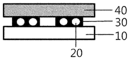
- FIG. 1 is a diagram illustrating an example of a structure of a light guide plate unit according to an exemplary embodiment of the present application.
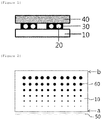
- FIG. 2 is a diagram illustrating an example of a pattern form of an adhesive layer according to the exemplary embodiment of the present application
- FIG. 3 is a diagram illustrating an example of a structure of a backlight unit according to the exemplary embodiment of the present application.
- FIG. 4 is a diagram illustrating an example of a structure of a liquid crystal display device according to the exemplary embodiment of the present application.
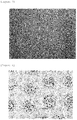
- FIGS. 5 and 6 are images representing forms of adhesive layers manufactured in the Examples.
- FIGS. 7 and 8 are images representing forms of adhesive layers manufactured in the Comparative Examples.
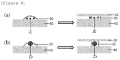
- FIG. 9 is a diagram illustrating an example of a change in the form of the adhesive layer according to the Examples and the Comparative Example of the present specification.
- a light guide plate unit includes a reflection plate, an adhesive layer which is provided on the reflection plate and includes a bead, and a light guide plate provided on the adhesive layer, and a size of the bead is 5 ⁇ m to 30 ⁇ m.
- FIG. 1 illustrates a structure of a light guide plate unit according to an exemplary embodiment of the present application.
- a size of the bead is 5 ⁇ m to 30 ⁇ m.
- the size of the bead means a maximum diameter value of the bead, and the size of the bead is a value measured by using a scanning electron microscope (SEM).
- a thickness and a width of the adhesive layer are uniform, so that there is an effect in that a space between the light guide plate and the reflection plate is maintained with a predetermined thickness, and adhesive strength is secured. Further, an air layer is secured on a lower surface of the light guide plate by the thickness of the adhesive layer, thereby achieving an effect in that total reflection of the light guide plate is possible.
- the adhesive layer is provided in a pattern form.
- the pattern means a protruding form, and the protruding form of the pattern may be a dot shape.
- two or more patterns of the adhesive layer are disposed while being spaced apart from one another.
- At least one of the pattern at a light entering portion side may be smaller than a pattern at a reverse light entering portion side.
- the size of the pattern may be increased from the light entering portion side toward the reverse light entering portion side.
- FIG. 2 is a diagram illustrating an example of a pattern form of the adhesive layer according to the exemplary embodiment of the present application.
- the pattern at the light entering portion side in the adhesive layer is smaller than the pattern of the reverse light entering portion side, there is an effect in that luminance is uniform.
- a width of an adhesive at the reverse light entering portion side is larger than a width of an adhesive at the light entering portion side, so that even though the quantity of light sources at the reverse light entering portion side is small, there is an effect in that luminance is uniform.
- the size of the pattern at the light entering portion side is the same as the size of the pattern at the reverse light entering portion side, but the densities of the patterns may be different.
- the density of the pattern may be increased from the light entering portion side toward the reverse light entering portion side.
- the increase in a density of the pattern means a decrease in a gap between the patterns.
- the light entering portion means the side of the light guide plate, to which the light source is irradiated
- the reverse light entering portion means the opposite side of the side of the light guide plate, to which the light source is irradiated.
- a represents the side of the light guide plate, to which the light source is irradiated, that is, the light entering portion
- b represents the opposite side of the side of the light guide plate, to which the light source is irradiated, that is, the reverse light entering portion.
- the size of the bead when the size of the bead is 5 ⁇ m to 30 ⁇ m, there is an effect in that a shape of the pattern is maintained without overlap of the patterns of the adhesive layer. Accordingly, there is an effect in achieving an effect according to a difference in a size and/or a density of the pattern between the light entering portion and the reverse light entering portion.
- the pattern of the adhesive layer may be formed by a screen printing method, a gravure printing method, or an inkjet printing method. Particularly, the pattern of the adhesive layer may be formed by a screen printing method.
- the adhesive layer includes a matrix resin.
- the matrix resin may be formed of a thermosetting resin or a photo-curable resin. Particularly, as thermosetting resin or the photo-curable resin, a urethane-based resin, an epoxy resin, an acryl-based resin, a silicon-based resin, a polysiloxane resin, a radically polymerizable compound, and the like may be used. That is, the matrix resin may include at least one of a urethane-based resin, an epoxy resin, an acryl-based resin, a silicon-based resin, a polysiloxane resin, a radically polymerizable compound. Compounds known in the art may be used as the radically polymerizable compound.
- the adhesive layer may further include a cross linking agent and a hardening agent, in addition to thermosetting resin or a photo-curable resin.
- a cross linking agent and a hardening agent in addition to thermosetting resin or a photo-curable resin.
- isocyanate and radical initiators may be used as the cross linking agent and the hardening agent, but the cross linking agent and the hardening agent are not limited thereto.
- the adhesive layer may additionally include light scattering particles.
- the light scattering particle may be TiO 2 or SiO 2 .
- a composition of the adhesive layer may include a bead and a matrix resin and may be a solventless type.
- the matrix resin included in the adhesive layer may be a solventless type.
- the solventless type means a type including no solvent.
- the matrix resin is the solventless type, so that a process of drying a solvent is not included, thereby achieving an effect in that process cost is decreased compared to a process including a solvent. Further, the matrix resin of the solventless type is used, so that there are effects in that a change in a size of a dot due to evaporation of a solvent is prevented, a screen mesh is prevented from being blocked, and a printing property is improved.
- a thickness of the adhesive layer is 5 ⁇ m to 30 ⁇ m.
- the thickness of the adhesive layer means a value obtained by measuring a thickness of a space between a surface of the reflection layer and the highest portion of the adhesive layer, and the size of the bead may be measured by using a scanning electron microscope (SEM).
- the thickness of the adhesive layer satisfies the range, there is an effect in that a thickness between the light guide plate and the reflection plate is uniform. That is, there is an effect in that a thickness between the light guide plate and the reflection plate is maintained with the range of 5 ⁇ m to 30 ⁇ m.
- the bead is an organic bead.
- the bead includes an organic bead including at least one of polymethylmethaacrylate (PMMA), polystyrene (PS), and a copolymer thereof.
- PMMA polymethylmethaacrylate
- PS polystyrene
- the content of bead is 0.5 phr to 5 phrs in comparison with the matrix resin.
- the content of bead is less than 0.5 phr, there is difficulty in uniformly maintaining a thickness between the light guide plate and the reflection plate, and when the content of bead is larger than 5 phr, there is a problem in that adhesive strength of the adhesive layer is degraded.
- a size of the pattern is 50 ⁇ m to 1,000 ⁇ m. Particularly, a size of the pattern is 50 ⁇ m to 800 ⁇ m. More particularly, a size of the pattern is 50 ⁇ m to 700 ⁇ m.
- a size of the pattern is a value obtained by measuring the portion of the pattern having the largest diameter, and the size of the pattern may be measured through a high magnification lens.
- the size of the pattern is a value obtained by measuring the portion of the pattern having the largest diameter.
- a gap between the patterns is 100 ⁇ m to 3,000 ⁇ m. Particularly, a gap between the patterns is 100 ⁇ m to 2,500 ⁇ m. More particularly, a gap between the patterns is 100 ⁇ m to 2,000 ⁇ m.
- a gap between the patterns is a value obtained by measuring a distance between the center portions of the respective patterns, and the gap between the patterns may be measured through a high magnification lens.
- the gap between the patterns satisfies the range, there is an effect in that the form of each pattern is hidden after passing through a light diffusion film and a prism sheet, and the like and is smoothly observed.
- the gap between the pattern is a value obtained by measuring a distance between the center portions of the respective patterns.
- the reflection plate may use a material used in the art, and for example, inorganic fillers, such as a calcium oxide or a titanium dioxide (TiO 2 ), or has an improved reflection characteristic by pores formed inside a base material, such as polyethyleneterephthalate (PET), may be used.
- a thickness of the reflection plate is 50 ⁇ m to 500 ⁇ m.
- the light guide plate may use a material used in the art, and for example, a glass light guide plate may be used.
- the light guide plate unit may be usefully applied to a backlight unit.
- a light source may be positioned on one surface of the light guide plate in the light guide plate unit.
- the light source may be a side-chain light source.
- FIG. 3 illustrates a structure of the backlight unit according to the exemplary embodiment of the present application.
- the aforementioned backlight unit is applied to a liquid crystal display device.
- the liquid crystal display device includes the aforementioned backlight unit as a constituent element
- the liquid crystal display device is not particularly limited.
- the liquid crystal display device may include a liquid crystal panel and the backlight unit.
- the liquid crystal panel may be provided on one surface of the light guide plate, in which the adhesive layer is not provided, in the backlight unit.
- FIG. 4 illustrates an example of the structure of the liquid crystal display device.
- the liquid crystal display device is not limited thereto, as necessary, a polarizing plate or an additional film, for example, a phase difference film, a light collecting sheet, and a diffusion sheet, may be additionally provided between the liquid crystal panel and the backlight unit.
- a composition for forming an adhesive layer was prepared by using a UV adhesive as a matrix resin, PMMA as a bead, and TiO 2 as light scattering particles, and the composition was screen-printed on a light guide plate.
- a light guide plate unit was manufactured by the same method as that of Example 1 except that a UV adhesive did not include a bead.
- Adhesive power of the adhesive layer was measured by a method corrected in ASTM D3330. Adhesive power was measured through 180° peel test, and a peel speed was set to 500 mm/min for the measurement. In Table 1 below, the case where the adhesive portion was ruptured after the measurement as the result of the experiment of the adhesive power is indicated “0”, and the case where the adhesive portion was not ruptured is indicated “X”.
- the form of the adhesive layer of Comparative Example 3 was measured by using a high magnification lens (KEYENCE Company, VK-X Series) and is represented in FIG. 8 .
- a dotted line represents a pattern during the printing of the adhesive
- an internal circle represents a region, in which the adhesive is left, after the reflection plate and the light guide plate are bonded.
- FIG. 8 it can be seen that the size of the pattern is decreased after the reflection plate and the light guide plate are bonded. This is a phenomenon observed because the bead having the large size is used, so that the adhesive layer cannot be pressed and the matrix resin cannot be spread in the case of Comparative Example 3, unlike Examples. As a result, the size of the pattern is decreased, so that an adhesive area is decreased and adhesive power is decreased.
- FIG. 9 is a diagram illustrating an example of a change in the form of the adhesive layer according to Examples 1 to 7 and Comparative Example 3 of the present specification.
- FIG. 9A is a diagram illustrating an example of a change in the form of the adhesive layer according to Examples 1 to 7, and it can be seen that when the adhesive layer including the organic bead having the size of 5 ⁇ m to 30 ⁇ m is applied on the light guide plate in a form of a pattern and the reflection plate is laminated, the adhesive layer is maintained without a change in the size of the pattern.
- FIG. 9A is a diagram illustrating an example of a change in the form of the adhesive layer according to Examples 1 to 7, and it can be seen that when the adhesive layer including the organic bead having the size of 5 ⁇ m to 30 ⁇ m is applied on the light guide plate in a form of a pattern and the reflection plate is laminated, the adhesive layer is maintained without a change in the size of the pattern.
- FIG. 9A is a diagram illustrating an example of a change
- 9B is a diagram illustrating an example of a change in the form of the adhesive layer according to Comparative Example 3, and it can be seen that when the adhesive layer including the organic bead having the large size is applied on the light guide plate in a form of a pattern and the reflection plate is laminated, the adhesive layer cannot be pressed and the matrix resin cannot be spread due to the size of the bead, so that the size of the pattern and the adhesive area are decreased.
- the adhesive layer including the organic bead having the size of 5 ⁇ m to 30 ⁇ m is included in the light guide plate unit, so that there are effects in that adhesive power between the light guide plate and the reflection plate is maintained and a thickness of the adhesive layer is uniform. Accordingly, there is an effect in that luminance in a surface direction is uniform.
Landscapes
- Physics & Mathematics (AREA)
- General Physics & Mathematics (AREA)
- Optics & Photonics (AREA)
- Nonlinear Science (AREA)
- Chemical & Material Sciences (AREA)
- Mathematical Physics (AREA)
- Crystallography & Structural Chemistry (AREA)
- Organic Chemistry (AREA)
- Inorganic Chemistry (AREA)
- Planar Illumination Modules (AREA)
- Liquid Crystal (AREA)
Abstract
Description
-
- 10: Reflection plate
- 20: Bead
- 30: Adhesive layer
- 40: Light guide plate
- 50: Light source
- 60: Pattern
- 70: Liquid crystal panel
- a: Light entering portion
- b: Reverse light entering portion
| TABLE 1 | ||||||
| Thick- | ||||||
| TiO2 | ness of | |||||
| Organic bead | 200 nm | Pat- | Adhe- | adhe- | ||
| Size | Content | Content | tern | sive | sive | |||
| Type | (μm) | (phr) | (phr) | shape | power | layer | ||
| Example 1 | |
10 | 1 | 1 | ◯ | ◯ | 10 | |
| Example 2 | PMMA | 5 | 1 | 1 | ◯ | ◯ | 5 | |
| Example 3 | PMMA | 5 | 1 | 0 | ◯ | ◯ | 5 | |
| Example 4 | PMMA | 5 | 5 | 1 | ◯ | ◯ | 5 | |
| Example 5 | PS | 7 | 3 | 1 | ◯ | ◯ | 7 | |
| Example 6 | PMMA | 15 | 0.5 | 1 | ◯ | ◯ | 15 | |
| Example 7 | PMMA | 28 | 0.5 | 1 | ◯ | ◯ | 28 | |
| Compar- | — | — | — | 1 | X | ◯ | 1~5 | |
| ative | ||||||||
| Example 1 | ||||||||
| Compar- | PS | 3 | 2 | 1 | X | ◯ | 3 | |
| ative | ||||||||
| Example 2 | ||||||||
| Compar- | |
40 | 0.5 | 1 | | X | 40 | |
| ative | ||||||||
| Example 3 | ||||||||
Claims (12)
Applications Claiming Priority (5)
| Application Number | Priority Date | Filing Date | Title |
|---|---|---|---|
| KR10-2016-0046470 | 2016-04-15 | ||
| KR20160046470 | 2016-04-15 | ||
| KR1020170047317A KR102155405B1 (en) | 2016-04-15 | 2017-04-12 | Light guide plate unit, back light unit and liquid crystal display comprising the same |
| KR10-2017-0047317 | 2017-04-12 | ||
| PCT/KR2017/004004 WO2017179923A1 (en) | 2016-04-15 | 2017-04-13 | Light guide plate unit, backlight unit comprising same, and liquid crystal display device |
Publications (2)
| Publication Number | Publication Date |
|---|---|
| US20190094455A1 US20190094455A1 (en) | 2019-03-28 |
| US10591663B2 true US10591663B2 (en) | 2020-03-17 |
Family
ID=60299907
Family Applications (1)
| Application Number | Title | Priority Date | Filing Date |
|---|---|---|---|
| US16/082,485 Active US10591663B2 (en) | 2016-04-15 | 2017-04-13 | Light guide plate unit, backlight unit comprising same, and liquid crystal display device |
Country Status (5)
| Country | Link |
|---|---|
| US (1) | US10591663B2 (en) |
| EP (1) | EP3444659B1 (en) |
| JP (1) | JP6805458B2 (en) |
| KR (1) | KR102155405B1 (en) |
| CN (1) | CN108885370B (en) |
Families Citing this family (1)
| Publication number | Priority date | Publication date | Assignee | Title |
|---|---|---|---|---|
| JP7422336B2 (en) * | 2021-07-28 | 2024-01-26 | 日亜化学工業株式会社 | Planar light source |
Citations (29)
| Publication number | Priority date | Publication date | Assignee | Title |
|---|---|---|---|---|
| JPH09202871A (en) | 1996-01-25 | 1997-08-05 | Lintec Corp | Adhesive for planar light source and planar light source using the same |
| US20050030630A1 (en) | 2001-09-27 | 2005-02-10 | Arataka Ohnishi | Reflective film |
| US20050259194A1 (en) | 2004-05-18 | 2005-11-24 | Lee Jeong-Hwan | Liquid crystal display and reflecting member for the same |
| KR20060079986A (en) | 2005-01-04 | 2006-07-07 | 삼성전자주식회사 | Liquid crystal display |
| KR20080032753A (en) | 2006-10-10 | 2008-04-16 | 삼성전자주식회사 | Ink for pattern formation, manufacturing method thereof, light guide plate, light emitting unit and liquid crystal display device having the same |
| US20080130263A1 (en) * | 2006-11-30 | 2008-06-05 | Lite-On Technology Corporation | Thin light-guiding structure and electronic device using the same |
| US20090284149A1 (en) * | 2008-05-15 | 2009-11-19 | Hidenori Koshikawa | Light-emitting device |
| US20100157623A1 (en) * | 2008-12-17 | 2010-06-24 | Sony Corporation | Planar light-emitting apparatus |
| KR20110028391A (en) | 2008-07-10 | 2011-03-17 | 쓰리엠 이노베이티브 프로퍼티즈 컴파니 | Retroreflective articles and devices having viscoelastic light guides |
| US20110096567A1 (en) * | 2009-10-28 | 2011-04-28 | Texas Instruments Incorporated. | Light guide plate and backlight module |
| US20110122094A1 (en) * | 2009-11-25 | 2011-05-26 | Coretronic Corporation | Optical touch apparatus and optical touch display apparatus |
| US20110163066A1 (en) * | 2010-01-06 | 2011-07-07 | Samsung Electronics Co., Ltd. | Methods of manufacturing surface light source devices |
| KR101070694B1 (en) | 2011-04-26 | 2011-10-11 | (주)케이앤씨엘이디 | Light guide plate manufacturing sheet |
| WO2012043396A1 (en) | 2010-09-27 | 2012-04-05 | 古河電気工業株式会社 | Backlight panel and reflection plate for backlight panel |
| US20120287677A1 (en) * | 2009-12-08 | 2012-11-15 | 3M Innovative Properties Company | Optical constructions incorporating a light guide and low refractive index films |
| KR20120128498A (en) | 2011-05-17 | 2012-11-27 | 한국건설생활환경시험연구원 | Diffusive ink composition comprising polymethylmethacrylate bead |
| KR101244188B1 (en) | 2005-02-28 | 2013-03-18 | 가부시키가이샤 구라레 | Photodiffusion film, planar light source element using the same, and liquid crystal display device |
| US20130100704A1 (en) * | 2011-10-25 | 2013-04-25 | Unipixel Displays, Inc. | Light guide with a printed film |
| KR20130084554A (en) | 2012-01-17 | 2013-07-25 | (주)케이앤씨엘이디 | Light reflection plate |
| US20130235614A1 (en) * | 2010-01-13 | 2013-09-12 | Martin B. Wolk | Illumination device having viscoelastic lightguide |
| KR20140022329A (en) | 2012-08-13 | 2014-02-24 | (주)케이앤씨엘이디 | Light guide plate and sheet for manufacturing light guide plate |
| KR101392506B1 (en) | 2013-06-27 | 2014-05-07 | 명범영 | Light guide panel unit consisting of light guide panel attached with reflection sheet for scattered reflection of light |
| KR20140080743A (en) | 2012-12-14 | 2014-07-01 | 엘지디스플레이 주식회사 | Optical film and back light unit thereof |
| KR101424737B1 (en) | 2013-09-24 | 2014-08-01 | 주식회사 에이치지엠 | Surface lighting device based on light guide panel |
| US20150189703A1 (en) * | 2013-12-27 | 2015-07-02 | Nichia Corporation | Light emitting device |
| KR101537060B1 (en) | 2013-12-16 | 2015-07-15 | 한국신발피혁연구원 | Ultraviolet―curable ink binder composition for light guide plate |
| KR101536275B1 (en) | 2014-12-05 | 2015-07-15 | 주식회사 에스에프씨 | Reflective sheet for light guide plate |
| US20160238774A1 (en) * | 2013-08-28 | 2016-08-18 | Fujifilm Corporation | Light guide plate, backlight unit comprising same, liquid crystal display device and optical sheet |
| US20160299285A1 (en) * | 2015-04-13 | 2016-10-13 | Young Lighting Technology Inc. | Light source module |
Family Cites Families (9)
| Publication number | Priority date | Publication date | Assignee | Title |
|---|---|---|---|---|
| JPH1021720A (en) * | 1996-06-27 | 1998-01-23 | Nec Corp | Backlight device |
| JPH10206644A (en) * | 1997-01-21 | 1998-08-07 | Minebea Co Ltd | Surface light source device |
| KR20050110223A (en) * | 2004-05-18 | 2005-11-23 | 삼성전자주식회사 | Liquid crystal display |
| KR100719482B1 (en) * | 2004-09-13 | 2007-05-18 | 에스케이씨 주식회사 | Reflection sheets and back-light units employing the same |
| JP5437652B2 (en) * | 2009-01-30 | 2014-03-12 | 恵和株式会社 | Light guide sheet and backlight unit using the same |
| KR20110130606A (en) * | 2010-05-28 | 2011-12-06 | 삼성코닝정밀소재 주식회사 | Integrated light guide pannel and back light unit containing with it |
| TWI431346B (en) * | 2010-12-08 | 2014-03-21 | Young Lighting Technology Corp | Light guide module, backlight module and fabricating method for the light guide module |
| KR101251815B1 (en) * | 2011-11-07 | 2013-04-09 | 엘지이노텍 주식회사 | Optical sheet and display device having the same |
| CN103499853B (en) * | 2013-09-29 | 2014-06-25 | 杭州瑞辉光电科技有限公司 | Light guide plate, planar light emitting device, liquid crystal display device, liquid crystal display terminal equipment and manufacturing method of light guide plate |
-
2017
- 2017-04-12 KR KR1020170047317A patent/KR102155405B1/en not_active Expired - Fee Related
- 2017-04-13 EP EP17782678.1A patent/EP3444659B1/en active Active
- 2017-04-13 CN CN201780021192.6A patent/CN108885370B/en not_active Expired - Fee Related
- 2017-04-13 US US16/082,485 patent/US10591663B2/en active Active
- 2017-04-13 JP JP2018547462A patent/JP6805458B2/en not_active Expired - Fee Related
Patent Citations (31)
| Publication number | Priority date | Publication date | Assignee | Title |
|---|---|---|---|---|
| JPH09202871A (en) | 1996-01-25 | 1997-08-05 | Lintec Corp | Adhesive for planar light source and planar light source using the same |
| US20050030630A1 (en) | 2001-09-27 | 2005-02-10 | Arataka Ohnishi | Reflective film |
| US20050259194A1 (en) | 2004-05-18 | 2005-11-24 | Lee Jeong-Hwan | Liquid crystal display and reflecting member for the same |
| KR20060079986A (en) | 2005-01-04 | 2006-07-07 | 삼성전자주식회사 | Liquid crystal display |
| KR101244188B1 (en) | 2005-02-28 | 2013-03-18 | 가부시키가이샤 구라레 | Photodiffusion film, planar light source element using the same, and liquid crystal display device |
| KR20080032753A (en) | 2006-10-10 | 2008-04-16 | 삼성전자주식회사 | Ink for pattern formation, manufacturing method thereof, light guide plate, light emitting unit and liquid crystal display device having the same |
| US20080089097A1 (en) | 2006-10-10 | 2008-04-17 | Samsung Electronics Co., Ltd. | Pattern forming ink, method for fabricating the same, and light guide plate, light emitting unit, and liquid crystal display having the same |
| US20080130263A1 (en) * | 2006-11-30 | 2008-06-05 | Lite-On Technology Corporation | Thin light-guiding structure and electronic device using the same |
| US20090284149A1 (en) * | 2008-05-15 | 2009-11-19 | Hidenori Koshikawa | Light-emitting device |
| US20110122494A1 (en) | 2008-07-10 | 2011-05-26 | Sherman Audrey A | Retroreflective articles and devices having viscoelastic lightguide |
| KR20110028391A (en) | 2008-07-10 | 2011-03-17 | 쓰리엠 이노베이티브 프로퍼티즈 컴파니 | Retroreflective articles and devices having viscoelastic light guides |
| US20100157623A1 (en) * | 2008-12-17 | 2010-06-24 | Sony Corporation | Planar light-emitting apparatus |
| US20110096567A1 (en) * | 2009-10-28 | 2011-04-28 | Texas Instruments Incorporated. | Light guide plate and backlight module |
| US20110122094A1 (en) * | 2009-11-25 | 2011-05-26 | Coretronic Corporation | Optical touch apparatus and optical touch display apparatus |
| US20120287677A1 (en) * | 2009-12-08 | 2012-11-15 | 3M Innovative Properties Company | Optical constructions incorporating a light guide and low refractive index films |
| US20110163066A1 (en) * | 2010-01-06 | 2011-07-07 | Samsung Electronics Co., Ltd. | Methods of manufacturing surface light source devices |
| US20130235614A1 (en) * | 2010-01-13 | 2013-09-12 | Martin B. Wolk | Illumination device having viscoelastic lightguide |
| WO2012043396A1 (en) | 2010-09-27 | 2012-04-05 | 古河電気工業株式会社 | Backlight panel and reflection plate for backlight panel |
| KR101070694B1 (en) | 2011-04-26 | 2011-10-11 | (주)케이앤씨엘이디 | Light guide plate manufacturing sheet |
| KR20120128498A (en) | 2011-05-17 | 2012-11-27 | 한국건설생활환경시험연구원 | Diffusive ink composition comprising polymethylmethacrylate bead |
| US20130100704A1 (en) * | 2011-10-25 | 2013-04-25 | Unipixel Displays, Inc. | Light guide with a printed film |
| KR20130084554A (en) | 2012-01-17 | 2013-07-25 | (주)케이앤씨엘이디 | Light reflection plate |
| KR20140022329A (en) | 2012-08-13 | 2014-02-24 | (주)케이앤씨엘이디 | Light guide plate and sheet for manufacturing light guide plate |
| KR20140080743A (en) | 2012-12-14 | 2014-07-01 | 엘지디스플레이 주식회사 | Optical film and back light unit thereof |
| KR101392506B1 (en) | 2013-06-27 | 2014-05-07 | 명범영 | Light guide panel unit consisting of light guide panel attached with reflection sheet for scattered reflection of light |
| US20160238774A1 (en) * | 2013-08-28 | 2016-08-18 | Fujifilm Corporation | Light guide plate, backlight unit comprising same, liquid crystal display device and optical sheet |
| KR101424737B1 (en) | 2013-09-24 | 2014-08-01 | 주식회사 에이치지엠 | Surface lighting device based on light guide panel |
| KR101537060B1 (en) | 2013-12-16 | 2015-07-15 | 한국신발피혁연구원 | Ultraviolet―curable ink binder composition for light guide plate |
| US20150189703A1 (en) * | 2013-12-27 | 2015-07-02 | Nichia Corporation | Light emitting device |
| KR101536275B1 (en) | 2014-12-05 | 2015-07-15 | 주식회사 에스에프씨 | Reflective sheet for light guide plate |
| US20160299285A1 (en) * | 2015-04-13 | 2016-10-13 | Young Lighting Technology Inc. | Light source module |
Also Published As
| Publication number | Publication date |
|---|---|
| KR20170118610A (en) | 2017-10-25 |
| EP3444659B1 (en) | 2021-06-02 |
| CN108885370B (en) | 2021-10-26 |
| JP2019511092A (en) | 2019-04-18 |
| KR102155405B1 (en) | 2020-09-14 |
| EP3444659A4 (en) | 2019-02-27 |
| EP3444659A1 (en) | 2019-02-20 |
| JP6805458B2 (en) | 2020-12-23 |
| US20190094455A1 (en) | 2019-03-28 |
| CN108885370A (en) | 2018-11-23 |
Similar Documents
| Publication | Publication Date | Title |
|---|---|---|
| TWI327253B (en) | ||
| JP6526190B2 (en) | Polymerizable composition, wavelength conversion member, backlight unit, and liquid crystal display device | |
| TWI463216B (en) | Multi-functional optic sheet | |
| US20100246011A1 (en) | Optical film | |
| TWI474051B (en) | A light diffusing sheet and a backlight device using the same | |
| JP6706982B2 (en) | Area lighting device | |
| TW200304025A (en) | Light diffusive sheet and area light source element using the same | |
| JP6732045B2 (en) | Wavelength conversion film and backlight unit | |
| JP6691449B2 (en) | Area lighting device | |
| US20190302497A1 (en) | Wavelength conversion film and method of manufacturing wavelength conversion film | |
| TW201643652A (en) | Touch panel, display device, optical sheet, optical sheet selection method, and optical sheet manufacturing method | |
| JP2017021297A (en) | Quantum dot sheet, backlight and liquid crystal display device | |
| US8419259B2 (en) | Backlight unit | |
| US10591663B2 (en) | Light guide plate unit, backlight unit comprising same, and liquid crystal display device | |
| JP4968728B2 (en) | Light control film laminate for projection screen, method for manufacturing the same, and projection screen | |
| CN115706193A (en) | Optical laminate | |
| TWI765177B (en) | Anti-glare film, polarizing plate and display device | |
| JP2009103892A (en) | Light diffusing body | |
| TWI865442B (en) | Anti-glare film | |
| KR20120104220A (en) | Light diffusing sheet and backlight using same | |
| KR101269720B1 (en) | Diffuser Sheet and Brightness Enhancement Film | |
| KR101084573B1 (en) | Optical sheet | |
| TWI483043B (en) | Lighting unit and lcd using the same | |
| TWI386686B (en) | Preparation of Optical Film and Its Product | |
| KR20140084617A (en) | Optical Sheet |
Legal Events
| Date | Code | Title | Description |
|---|---|---|---|
| FEPP | Fee payment procedure |
Free format text: ENTITY STATUS SET TO UNDISCOUNTED (ORIGINAL EVENT CODE: BIG.); ENTITY STATUS OF PATENT OWNER: LARGE ENTITY |
|
| AS | Assignment |
Owner name: LG CHEM, LTD., KOREA, REPUBLIC OF Free format text: ASSIGNMENT OF ASSIGNORS INTEREST;ASSIGNORS:YOO, HAN SOL;KO, DONG HO;AHN, BYEONG IN;AND OTHERS;SIGNING DATES FROM 20170720 TO 20170723;REEL/FRAME:047024/0068 |
|
| STPP | Information on status: patent application and granting procedure in general |
Free format text: DOCKETED NEW CASE - READY FOR EXAMINATION |
|
| STPP | Information on status: patent application and granting procedure in general |
Free format text: NON FINAL ACTION MAILED |
|
| STPP | Information on status: patent application and granting procedure in general |
Free format text: FINAL REJECTION MAILED |
|
| STPP | Information on status: patent application and granting procedure in general |
Free format text: NOTICE OF ALLOWANCE MAILED -- APPLICATION RECEIVED IN OFFICE OF PUBLICATIONS |
|
| STPP | Information on status: patent application and granting procedure in general |
Free format text: PUBLICATIONS -- ISSUE FEE PAYMENT VERIFIED |
|
| STCF | Information on status: patent grant |
Free format text: PATENTED CASE |
|
| MAFP | Maintenance fee payment |
Free format text: PAYMENT OF MAINTENANCE FEE, 4TH YEAR, LARGE ENTITY (ORIGINAL EVENT CODE: M1551); ENTITY STATUS OF PATENT OWNER: LARGE ENTITY Year of fee payment: 4 |