US10586876B2 - Schottky device and method of manufacturing the same - Google Patents
Schottky device and method of manufacturing the same Download PDFInfo
- Publication number
- US10586876B2 US10586876B2 US15/705,242 US201715705242A US10586876B2 US 10586876 B2 US10586876 B2 US 10586876B2 US 201715705242 A US201715705242 A US 201715705242A US 10586876 B2 US10586876 B2 US 10586876B2
- Authority
- US
- United States
- Prior art keywords
- region
- drift layer
- buffer
- layer
- trench
- Prior art date
- Legal status (The legal status is an assumption and is not a legal conclusion. Google has not performed a legal analysis and makes no representation as to the accuracy of the status listed.)
- Active
Links
Images


Classifications
-
- H—ELECTRICITY
- H10—SEMICONDUCTOR DEVICES; ELECTRIC SOLID-STATE DEVICES NOT OTHERWISE PROVIDED FOR
- H10D—INORGANIC ELECTRIC SEMICONDUCTOR DEVICES
- H10D8/00—Diodes
- H10D8/60—Schottky-barrier diodes
-
- H—ELECTRICITY
- H10—SEMICONDUCTOR DEVICES; ELECTRIC SOLID-STATE DEVICES NOT OTHERWISE PROVIDED FOR
- H10D—INORGANIC ELECTRIC SEMICONDUCTOR DEVICES
- H10D8/00—Diodes
- H10D8/50—PIN diodes
-
- H01L29/872—
-
- H01L29/0619—
-
- H01L29/1608—
-
- H01L29/267—
-
- H01L29/36—
-
- H01L29/47—
-
- H01L29/6606—
-
- H01L29/66143—
-
- H—ELECTRICITY
- H10—SEMICONDUCTOR DEVICES; ELECTRIC SOLID-STATE DEVICES NOT OTHERWISE PROVIDED FOR
- H10D—INORGANIC ELECTRIC SEMICONDUCTOR DEVICES
- H10D62/00—Semiconductor bodies, or regions thereof, of devices having potential barriers
- H10D62/10—Shapes, relative sizes or dispositions of the regions of the semiconductor bodies; Shapes of the semiconductor bodies
- H10D62/102—Constructional design considerations for preventing surface leakage or controlling electric field concentration
- H10D62/103—Constructional design considerations for preventing surface leakage or controlling electric field concentration for increasing or controlling the breakdown voltage of reverse-biased devices
- H10D62/105—Constructional design considerations for preventing surface leakage or controlling electric field concentration for increasing or controlling the breakdown voltage of reverse-biased devices by having particular doping profiles, shapes or arrangements of PN junctions; by having supplementary regions, e.g. junction termination extension [JTE]
- H10D62/106—Constructional design considerations for preventing surface leakage or controlling electric field concentration for increasing or controlling the breakdown voltage of reverse-biased devices by having particular doping profiles, shapes or arrangements of PN junctions; by having supplementary regions, e.g. junction termination extension [JTE] having supplementary regions doped oppositely to or in rectifying contact with regions of the semiconductor bodies, e.g. guard rings with PN or Schottky junctions
-
- H—ELECTRICITY
- H10—SEMICONDUCTOR DEVICES; ELECTRIC SOLID-STATE DEVICES NOT OTHERWISE PROVIDED FOR
- H10D—INORGANIC ELECTRIC SEMICONDUCTOR DEVICES
- H10D62/00—Semiconductor bodies, or regions thereof, of devices having potential barriers
- H10D62/60—Impurity distributions or concentrations
-
- H—ELECTRICITY
- H10—SEMICONDUCTOR DEVICES; ELECTRIC SOLID-STATE DEVICES NOT OTHERWISE PROVIDED FOR
- H10D—INORGANIC ELECTRIC SEMICONDUCTOR DEVICES
- H10D62/00—Semiconductor bodies, or regions thereof, of devices having potential barriers
- H10D62/80—Semiconductor bodies, or regions thereof, of devices having potential barriers characterised by the materials
- H10D62/82—Heterojunctions
-
- H—ELECTRICITY
- H10—SEMICONDUCTOR DEVICES; ELECTRIC SOLID-STATE DEVICES NOT OTHERWISE PROVIDED FOR
- H10D—INORGANIC ELECTRIC SEMICONDUCTOR DEVICES
- H10D62/00—Semiconductor bodies, or regions thereof, of devices having potential barriers
- H10D62/80—Semiconductor bodies, or regions thereof, of devices having potential barriers characterised by the materials
- H10D62/83—Semiconductor bodies, or regions thereof, of devices having potential barriers characterised by the materials being Group IV materials, e.g. B-doped Si or undoped Ge
- H10D62/832—Semiconductor bodies, or regions thereof, of devices having potential barriers characterised by the materials being Group IV materials, e.g. B-doped Si or undoped Ge being Group IV materials comprising two or more elements, e.g. SiGe
- H10D62/8325—Silicon carbide
-
- H—ELECTRICITY
- H10—SEMICONDUCTOR DEVICES; ELECTRIC SOLID-STATE DEVICES NOT OTHERWISE PROVIDED FOR
- H10D—INORGANIC ELECTRIC SEMICONDUCTOR DEVICES
- H10D64/00—Electrodes of devices having potential barriers
- H10D64/60—Electrodes characterised by their materials
- H10D64/64—Electrodes comprising a Schottky barrier to a semiconductor
-
- H—ELECTRICITY
- H10—SEMICONDUCTOR DEVICES; ELECTRIC SOLID-STATE DEVICES NOT OTHERWISE PROVIDED FOR
- H10D—INORGANIC ELECTRIC SEMICONDUCTOR DEVICES
- H10D8/00—Diodes
- H10D8/01—Manufacture or treatment
-
- H—ELECTRICITY
- H10—SEMICONDUCTOR DEVICES; ELECTRIC SOLID-STATE DEVICES NOT OTHERWISE PROVIDED FOR
- H10D—INORGANIC ELECTRIC SEMICONDUCTOR DEVICES
- H10D8/00—Diodes
- H10D8/01—Manufacture or treatment
- H10D8/051—Manufacture or treatment of Schottky diodes
-
- H01L29/0692—
-
- H—ELECTRICITY
- H10—SEMICONDUCTOR DEVICES; ELECTRIC SOLID-STATE DEVICES NOT OTHERWISE PROVIDED FOR
- H10D—INORGANIC ELECTRIC SEMICONDUCTOR DEVICES
- H10D62/00—Semiconductor bodies, or regions thereof, of devices having potential barriers
- H10D62/10—Shapes, relative sizes or dispositions of the regions of the semiconductor bodies; Shapes of the semiconductor bodies
- H10D62/124—Shapes, relative sizes or dispositions of the regions of semiconductor bodies or of junctions between the regions
- H10D62/126—Top-view geometrical layouts of the regions or the junctions
Definitions
- the present invention relates to a semiconductor device, and more particularly to a Schottky device.
- Schottky devices include a Schottky junction formed between a semiconductor layer and a metal layer.
- the Schottky devices are characterized by a lower forward voltage drop and a faster switching action compared with general PN junction diodes.
- Silicon carbide is a wide-gap semiconductor material with a forbidden band gap between 2.35 eV and 3.28 eV.
- a SiC-based semiconductor is thermally, chemically and mechanically stable and is suitable for applications where high power, high speed, high temperature are required.
- the Schottky device includes a silicon carbide (SiC) substrate of a first conductivity type, a drift layer, a trench, a barrier layer of a second conductivity type opposite the first conductivity type, an electrically conductive material, a first electrode, and a second electrode.
- the drift layer is formed of SiC and is situated onto the SiC substrate.
- the drift layer has the first conductivity type with an impurity concentration lower than that of the SiC substrate.
- the drift layer has a top surface and a bottom surface with the bottom surface contacting the SiC substrate.
- the trench extends from the top surface of the drift layer towards the SiC substrate.
- the barrier layer contacts the drifting layer and covers a sidewall and a bottom wall of the trench.
- the electrically conductive material at least partially fills the trench and contacts the barrier layer.
- the first electrode is situated on the top surface of the drift layer.
- the first electrode forms a Schottky junction with the drift layer and forms a low resistivity contact with the barrier layer and the electrically conductive material.
- the second electrode forms an ohmic contact with the SiC substrate.
- the barrier layer includes a buffer junction barrier (JB) sub layer with a first impurity concentration and a JB layer with a second impurity concentration.
- the first impurity concentration is lower than the second impurity concentration.
- FIG. 1A illustrates a Schottky device with a planar structure in accordance with an example embodiment.
- FIG. 1B illustrates a junction barrier (JB) region enclosed by more than one buffer JB sub region in accordance with an example embodiment.
- JB junction barrier
- FIG. 2 illustrates a top view of JB regions and buffer JB sub regions in accordance with an example embodiment.
- FIG. 3 illustrates a top view of JB regions and buffer JB sub regions in accordance with another example embodiment.
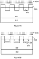
- FIG. 4A shows a graph illustrating a performance comparison between a Schottky device with a planar structure in accordance with an example embodiment and a conventional Schottky device.
- FIG. 4B is a table showing values for current leakage for a Schottky device with a planar structure in accordance with an example embodiment and a conventional Schottky device.
- FIG. 5 illustrates a Schottky device with a shallow trench in accordance with an example embodiment.
- FIG. 6 illustrates a Schottky device with a deep trench in accordance with an example embodiment.
- FIG. 7 illustrates a Schottky device with a deep trench in accordance with another example embodiment.
- FIG. 8 illustrates a method that manufactures a Schottky device in accordance with an example embodiment.
- FIG. 9A illustrates forming a JB region by using an oxide layer as a hard mask in accordance with an example embodiment.
- FIG. 9B illustrates forming a buffer JB sub region by using an oxide layer as a hard mask in accordance with an example embodiment.
- FIG. 10 illustrates a method that manufactures a Schottky device in accordance with an example embodiment.
- FIG. 11 illustrates a method that manufactures a Schottky device in accordance with an example embodiment.
- Example embodiments relate to Schottky devices with novel structure designs and improved performances, such as improved leakage and breakdown voltages.
- Si-based manufacturing processes Silicon carbide (SiC)-based devices due to differences in their material properties.
- Si-based process an initial doping profile is generally formed with ion implantation. Initial overlap of the initial doping profile is not smooth and needs a thermal anneal to facilitate dopant redistribution to form an expected profile.
- this does not work well for SiC material as there is almost no dopant redistribution in SiC material during thermal anneal.
- the doping profile remains choppy and weak spots are formed that increase current leakage
- One or more example embodiments solve one or more of the technical problems associated with conventional Schottky devices as set forth above.
- One or more example embodiments achieve Schottky devices with improved device performance by providing newly-designed device structures and manufacturing processes to contribute to semiconductor technology.
- One or more example embodiments achieve Schottky devices with improved performance, such as reduced leakage and improved breakdown voltage.
- one example embodiment demonstrates a Schottky device with leakage approximately five times lower than that of its conventional counterparts.
- Advantages of example embodiments further include the proposed novel processes for manufacturing Schottky devices, which can be implemented with one or more benefits of simplicity, flexibility, and better alignment, etc. These novel processes overcome the non-transferability of Si-based process when manufacturing SiC-based devices.
- Schottky devices of example embodiments have broader and better applications compared with conventional Schottky devices.
- Example embodiments includes a Schottky device with a planar structure, a shallow trench structure, and a deep trench structure respectively.
- a junction barrier (JB) region is enclosed by a buffer JB sub region with a lower impurity concentration compared with the JB region. Both the JB region and the buffer JB sub region have the conductivity type opposite that of a drift region.
- the buffer JB sub region is designed or configured such that a regulated doping junction is formed between the JB region and the Schottky region. As such, the maximal electric field between the JB region and Schottky region as well as the metal Schottky barrier is reduced, thereby improving overall performance for the Schottky device.
- One or more example embodiments recognize that leakage mostly happens at the bottom and corners of the JB region and the surface of the Schottky junction or area under the Schottky metal.
- Enclosure of the JB region by the buffer JB sub region at the bottom is designed to be larger than that at the sidewall of the JB region or lateral enclosure.
- the lateral enclosure and the bottom enclosure can be independently adjusted or obtained, for example, by designing process parameters.
- the lateral enclosure can be designed optimally to reduce electric field at the sidewall of the JB region on one hand, and maintain a low turn-on resistance for the Schottky junction on the other hand, thereby achieving optimal performance.
- forward voltage drop for the Schottky junction is prevented from increasing and can be retained at a low value, which contributes to fast switching speed and lower power consumption.
- One or more example embodiments include novel manufacturing process for the Schottky devices.
- the JB regions and the buffer JB sub regions are formed by ion implantations without relying on or attributable to dopant redistribution.
- a single oxide hard mask can be employed in formation of both the JB regions and the buffer JB sub regions with ion implantations, thereby self-alignment is achieved.
- a novel process including epitaxial growth is provided with simplicity and flexibility.
- FIG. 1A illustrates a Schottky device 100 with a planar structure in accordance with an example embodiment.
- the Schottky device 100 includes a substrate 110 , a drift layer or region 120 , one or more junction barrier (JB) regions or layers 126 , one or more buffer JB sub regions or layers 128 , an anode or first electrode or first metal layer 130 , and a cathode or second electrode or second metal layer 140 .
- JB junction barrier
- the substrate 110 has a first surface 112 and a second surface 114 opposite the first surface 112 .
- the substrate 110 includes or is formed of silicon carbide (SiC) of a first conductivity type (e.g., n-type).
- SiC silicon carbide
- the substrate 110 is highly n-doped SiC with an impurity or doping concentration of 5.0E19 cm ⁇ 3 (i.e. 5.0 ⁇ 10 19 cm ⁇ 3 ,) or greater.
- the drift layer 120 is situated or disposed on the substrate 110 .
- the drift layer 120 has a top surface 122 and a bottom surface 124 .
- the bottom surface 124 contacts the first surface 112 of the substrate 110 .
- the drift layer 120 includes dopants or impurities of the first conductivity type with an impurity concentration lower than that of the substrate 110 .
- the drift layer 120 is n-doped with a concentration in a range from 5.0E14 cm ⁇ 3 to 2.0E16 cm ⁇ 3 and has a thickness range from 5 micrometer (um) to 80 um.
- the impurity concentration of the drift layer 120 is 8.5E15 cm ⁇ 3 .
- the drift layer 120 is n-doped SiC that is epitaxially grown onto the substrate 110 .
- the JB region 126 is included in the drift layer 120 and extends from the top surface 122 towards the substrate 110 .
- the JB region 126 has a width w J and a depth d J beneath the top surface 122 .
- the width w J varies in a range from 0.5 um to 4.0 um
- the depth d J varies in a range from 0.3 um to 1.0 um.
- the JB region 126 includes dopants of a second conductivity type (e.g., p-type) opposite the first conductivity type and has a first impurity concentration.
- the JB region 126 can be formed by ion implantation.
- the buffer JB sub region 128 is included in the drift layer 120 and extends from the top surface 122 towards the substrate 110 .
- the buffer JB sub region 128 has a width w b and a depth d b .
- the depth d b is in a range from 0.7 um to 1.5 um.
- the width w b is larger than the width w J by 0.6 um to 2.0 um (i.e., lateral enclosure of the JB region 126 by the buffer JB sub region 128 is in a range from 0.3 um to 1.0 um per side).
- the buffer JB sub region 128 encloses the JB region 126 with a lateral enclosure dimension (i.e., (w b ⁇ w J )/2) and a bottom enclosure dimension (i.e., d b ⁇ d J ).
- the lateral enclosure dimension is smaller than the bottom enclosure dimension.
- the lateral enclosure dimension and the bottom enclosure dimension are adjustable independent on each other.
- the buffer JB sub region cannot effectively shield the Schottky junction under reverse bias and cannot effectively reduce the maximal electric field at the interface of the JB region and the Schottky region (As used herein, the “Schottky region” refers to the region between the JB regions in the drift layer 120 where Schottky junction is formed at the surface), thereby being not effective in reducing leakage and increasing breakdown voltage.
- the lateral enclosure dimension is too large, it will reduce the area of Schottky junction and thus reduce the forward current of the Schottky device.
- the capability of independently adjusting the lateral enclosure dimension in accordance with example embodiments are favorable or useful because an optimal lateral enclosure dimension can be achieved without negatively influencing other device parameters, such as depths and impurity concentrations of the JB regions and the buffer JB sub regions.
- Schottky device in accordance with example embodiments can be designed and manufactured with flexibility.
- the buffer JB sub region 128 fully encloses the JB region 126 in relation to sidewall and bottom wall. In this manner, the buffer JB sub region 128 provides effective shielding for the JB region 126 such that the maximal electric field between the JB region 126 and the Schottky region is reduced and overall performance for the Schottky device is improved.
- the buffer JB sub region 128 is of the second conductivity type with a second impurity concentration that is smaller than the first impurity concentration.
- the first impurity concentration is in a range from 7.0E18 cm ⁇ 3 to 6.0E20 cm ⁇ 3
- the second impurity concentration is in a range from 1.0E17 cm ⁇ 3 to 6.0E18 cm ⁇ 3 .
- the JB region 126 and the buffer JB sub region 128 can include dopants of same or different species.
- the JB region 126 includes dopants of aluminum (Al)
- the buffer JB sub region 128 includes one or more dopants selected from a group consisting of Al, Boron (B), and Gallium (Ga).
- the anode 130 is situated on the top surface 122 of the drift layer 120 .
- the anode 130 forms a Schottky junction with exposed portions of the top surface 122 of the drift layer 120 , and forms a low resistivity contact with the JB region 126 .
- the anode 130 can be a metal layer, such as aluminum (Al), titanium (Ti), nickel (Ni), or can be a multi-metal structure formed of two or more metals.
- the anode 130 includes multiple metal structures that are short-circuited.
- the cathode 140 contacts the second surface 114 to form a low resistivity contact with the substrate 110 .
- the cathode 140 includes one or more metals, such as nickel (Ni), titanium (Ti), silver (Ag), platinum (Pt), gold (Au) or the like that is capable of forming an ohmic contact with the SiC substrate.
- FIG. 1A illustrates three sets of JB region and buffer JB sub region, and each set illustratively includes one JB region and one buffer JB sub region
- each set can include multiple layers of buffer JB sub regions with regulated doping profiles according to practical requirements.
- FIG. 1B illustrates a JB region 126 , and three buffer JB sub regions 1281 , 1282 , and 1283 in the drift layer 120 in accordance with an example embodiment.
- the impurity concentration decreases from the JB region 126 towards the buffer JB sub region 1283 .
- the shapes of the JB region and the buffer JB sub region from a top or plane view can be predetermined or designed.
- the shapes can be circular, square, hexagonal, strip, or other suitable shapes according to practical requirements. This is illustrated in FIGS. 2 and 3 .
- FIG. 2 illustrates a top view of JB regions and buffer JB sub regions in accordance with an example embodiment. As illustrated, both the JB regions 226 and the buffer JB sub regions 228 are square shape on the top surface of the drift layer 220 .
- FIG. 3 illustrates a top view of JB regions and buffer JB sub regions in accordance with another example embodiment. As illustrated, both the JB regions 326 and the buffer JB sub regions 328 are circular shape on the top surface of the drift layer 320 .
- the Schottky device with structure as shown in FIG. 1A reduces maximum electric field at the junction formed at an interface between the JB region and the drift layer or Schottky region, thereby reducing reverse current leakage and increasing breakdown voltage.
- FIGS. 2 and 3 are for illustrative purpose only. A person having ordinary skill in the art would appreciate that the shapes for the JB regions and the buffer JB sub regions from a top view can be other suitable shapes, such as rectangular shape, stripe shape etc., according to practical requirements.
- FIG. 4A shows a graph 410 illustrating a performance comparison between a Schottky device with structure with reference to FIG. 1A (“Buffer JBS”) and a conventional Schottky device (“Std JBS”).
- FIG. 4B is a table 420 showing values of leakage current.
- the “Buffer JBS” includes a SiC drift layer of 11 um in thickness and being n-doped with an impurity concentration of 8.5E15 cm ⁇ 3 .
- d J 0.4 um
- w J 2.0 um
- d b 0.9 um
- w b 3.0 um
- w 0 3.0 um.
- the breakdown voltage is above 1200V.
- the “Std JBS” includes only a JB region without a Buffer JB sub region.
- the width and depth for the JB region of the “Std JBS” are 3.0 um and 0.9 um respectively.
- the JB region of the “Std JBS” has a same impurity concentration as that for the JB region of the “Buffer JBS”.
- the median leakage current for the “Buffer JBS” is 2.6 uA, which is about 5 times lower than that for the “Std JBS” (12.2 uA).
- the leakage currents for “Buffer JBS” group are more stable with less variation compare to the standard JBS structure.
- FIG. 5 illustrates a Schottky device 500 with a shallow trench in accordance with an example embodiment.
- the Schottky device 500 includes a substrate 510 with a first surface 512 and a second surface 514 , a drift layer 520 with a top surface 522 and a bottom surface 524 , one or more trenches 525 , one or more junction barrier (JB) regions 526 , one or more buffer JB sub regions 528 , an anode or first electrode or first metal layer 530 , and a cathode or second electrode or second metal layer 540 .
- both the substrate 510 and the drift layer 520 include SiC material of a first conductivity type (e.g., n-type).
- the trench 525 is formed in the drift layer 520 and extends from the top surface 522 of the drift layer 520 towards the substrate 510 .
- the trench 525 has a width w st and a depth d st beneath the top surface 522 of the drift layer 520 .
- the width w st is in a range from 0.5 um to 3.0 um
- the depth d st is in a range from 0.5 um to 1.5 um.
- the trench 525 is at least partially filled with one or more electrically conductive materials 529 , such as p-doped poly-Si, metal (e.g., Al, Ti, Ni, etc), and the like.
- the JB region 526 is included in the drift layer 520 and extends from the top surface 522 towards the substrate 510 .
- the JB region 526 encloses the trench 525 in relation to the sidewall and bottom of the trench 525 .
- the JB region 526 has a width w J and a depth d stJ beneath the bottom of the trench 525 .
- the depth d stJ is in a range from 0.8 um to 1.8 um.
- the width w J is in a range from 1 um to 4 um.
- the JB region 526 encloses the trench 525 with a lateral enclosure in a range from 0.25 um to 0.5 um.
- the JB region 526 includes dopants of a second conductivity type (e.g., p-type) opposite the first conductivity type and with a first impurity concentration.
- a second conductivity type e.g., p-type
- the buffer JB sub region 528 is included in the drift layer 520 and extends from the top surface 522 towards the substrate 510 .
- the buffer JB sub region 528 has a width w b and a depth d stb beneath the bottom of the trench 525 .
- the depth d stb is in a range from 1.1 um to 2.4 um.
- the width w b is in a range from 1.5 um to 5 um.
- the buffer JB sub region 528 encloses the JB region 526 with a lateral enclosure in a range from 0.25 um to 0.5 um.
- the buffer JB sub region 528 encloses the JB region 526 with a lateral enclosure dimension (i.e., (w b ⁇ w J )/2) and a bottom enclosure dimension (i.e., d stb ⁇ d stJ ).
- the lateral enclosure dimension is smaller than the bottom enclosure dimension.
- the lateral enclosure dimension can be adjusted independent on the bottom enclosure dimension.
- the buffer JB sub region 528 includes dopants of the second conductivity type (e.g., p-type) and with a second impurity concentration.
- the doping concentration for the buffer JB sub region 528 is lower than that for the JB region 526 such that maximal electric filed at PN junctions between the JB region 526 and the drift layer 520 under reverse voltage is reduced, thereby improving overall device performance, such as leakage and breakdown voltage.
- the JB region 526 and the buffer JB sub region 528 have same dopant specie selected from a group consisting of Aluminum (Al), Boron (B), and Gallium (Ga). In another example embodiment, the JB region 526 and the buffer JB sub region 528 have different dopant species selected from a group consisting of Al, B, and Ga.
- the distance w 1 between two adjacent buffer JB sub regions from two adjacent sets respectively is in a range from 2 um to 6 um.
- the buffer JB sub region 528 includes plural buffer JB sub regions with each having a different impurity concentration.
- the first metal layer 530 disposed on the drift layer 520 .
- the first metal layer 530 forms a Schottky junction with exposed portions of the drift layer 520 , and forms a low resistivity contact with the JB region and the one or more electrically conductive materials 529 .
- the second metal layer 540 form an ohmic contact with the SiC substrate 510 .
- thickness of drift layer 12.0 um
- w st 1.0 um
- w J 1.4 um
- w b 2.0 um
- d st 0.8 um
- d stJ 1.1 um
- d stb 1.5 um
- w 1 3.0 um
- the SiC Schottky device with such parameters has a breakdown voltage of greater than 1200V.
- FIG. 6 illustrates a Schottky device 600 with a deep trench in accordance with an example embodiment.
- the Schottky device 600 includes a substrate 610 , a drift layer 620 , one or more trenches 625 , one or more barrier layers or regions 627 , an anode or first metal layer 630 , and a cathode or second metal layer 640 .
- the substrate 610 has a first surface 612 and a second surface 614 .
- the substrate 610 includes SiC of a first conductivity type (e.g., n-type).
- the drift layer 620 is situated or disposed on the substrate 610 .
- the drift layer 620 has a top surface 622 and a bottom surface 624 .
- the drift layer 620 is of the first conductivity type with an impurity concentration lower than that of the substrate 610 .
- the thickness of the drift layer 620 is equal to or greater than 6.5 um.
- the trench 625 is formed in the drift layer 620 and extends from the top surface 622 towards the substrate 610 .
- the trench 625 has a width w dtB and a depth d dtB beneath the top surface 622 of the drift layer 620 .
- the width w dtB is in a range from 1.0 um to 3.0 um.
- the depth d dtB is in a range from 1.5 um to 5.0 um.
- the barrier layer or region 627 of a second conductivity type (e.g., p-type).
- the barrier layer 627 covers the sidewall and the bottom wall of the trench 625 and contacts the drifter layer 620 .
- the barrier layer 627 has a doping profile with an impurity concentration increasing from the drift layer 620 towards one or more electrically conductive materials 629 that at least partially fills the trench 625 .
- the barrier layer 627 is an epitaxial layer formed of one or more materials selected from a group consisting of Gallium nitride (GaN), and Silicon Carbide (SiC).
- the barrier layer 627 includes a buffer junction barrier (JB) sub layer with a first impurity concentration and a JB layer with a second impurity concentration.
- the buffer JB sub layer is sandwiched between the drift layer 620 and the JB layer.
- the first impurity concentration is lower than the second impurity concentration. This will be detailed later with reference to FIG. 7 .
- the rest of the trench 625 is at least partially filled with the one or more electrical materials 629 .
- the rest of the trench refers to internal space of the trench excluding the space occupied by the barrier layer.
- the barrier layer 627 is sandwiched between the one or more electrical materials 629 and the sidewall, the bottom wall of the trench 625 .
- the one or more electrical materials 629 are unnecessary. Instead, the whole trench 625 is filled with the barrier layer 627 .
- the barrier layer 627 includes both a JB region and a buffer JB sub region.
- the rest of the trench 625 has a width w dt and a depth d dt beneath the top surface 622 .
- the width w dt is in a range from 0 um to 2 um.
- the depth d dt is in a range from 0 um to 2.5 um.
- the distance w 2 between two adjacent trenches is in a range from 2 um to 6 um.
- the first metal layer 630 is situated on the drift layer 620 .
- the first metal layer 630 forms a Schottky junction with exposed portions of the top surface 622 of the drift layer 620 , and forms a low resistivity contact with the barrier layer 627 and the one or more electrically conductive materials 629 .
- the second metal layer 640 forms an ohmic contact with the SiC substrate 610 .
- thickness of drift layer 12.5 um
- w dt 0.6 um
- w dtB 1.6 um
- d dt 1.7 um
- d dtB 2.2 um
- w 2 3.0 um
- the SiC Schottky device with such parameters has a breakdown voltage of greater than 1200V.
- FIG. 7 illustrates a Schottky device 700 with a deep trench in accordance with another example embodiment.
- the Schottky device 700 includes a substrate 710 with a first surface 712 and a second surface 714 , a drift layer 720 with a top surface 722 and a bottom surface 724 , one or more trenches 725 , one or more electrically conductive materials 729 filled in the trench 725 , an anode or first metal layer 730 , and a cathode or second metal layer 740 .
- the barrier layer or region of Schottky device 700 includes a JB layer 726 and a buffer JB sub layer 728 .
- the buffer JB sub layer 728 is sandwiched between the drift layer 720 and the JB layer 726 .
- the buffer JB sub layer 728 covers the sidewall and the bottom wall of the trench 725 .
- the trench 725 has a width w dB and a depth d dB beneath the top surface 722 .
- the JB layer has a width w dJ and a depth d dJ beneath the top surface 722 .
- the rest of the trench 725 has a width wan and a depth data.
- the distance between two adjacent trenches is w 3 .
- FIG. 8 illustrates a method 800 that manufactures a Schottky device in accordance with an example embodiment.
- the method 800 is used to manufacture or produce the Schottky device 100 with reference to FIG. 1A with improved device performance.
- Block 802 states providing a SiC substrate.
- the SiC substrate is highly-doped with dopants of a first conductivity type, such as n-type dopants (e.g., Nitrogen, phosphorus, arsenic, etc.).
- dopants of a first conductivity type such as n-type dopants (e.g., Nitrogen, phosphorus, arsenic, etc.).
- Block 804 states epitaxially growing a SiC drift layer.
- the SiC drift layer is formed onto the SiC substrate with epitaxial growth with in-situ doping of the first conductivity type dopants.
- Block 806 states forming a junction barrier (JB) region.
- the JB region is formed by implanting dopants or impurities of a second conductivity type, such as p-type dopants (e.g., boron, aluminum, gallium, etc.), into a predetermined areas in the drift layer.
- the JB region is formed attributable to ion implantations rather than impurity diffusion process.
- Regulated doping profile is formed by adjusting parameters such as ion beam energy, implantation dose, tilt and twist angles, etc. A single implantation process, or multiple or repeated implantation processes can be employed according to practical requirements.
- the JB region is formed by using an oxide hard mask.
- a thick oxide layer e.g., silicon oxide
- Photoresist layer is formed (e.g., by spin-coating) onto the oxide layer and patterned with a mask such that portions of the oxide layer is isotropic etched to form one or more openings for selective implantation. Through these openings, by using the patterned oxide layer as a hard mask, dopant ions are implanted into the drift layer to form the JB region.
- the patterned oxide layer as a hard mask Usage of the patterned oxide layer as a hard mask is illustrated in FIG. 9A .
- the oxide layer is patterned (e.g., by wet etching or dry etching, or combination of both) to expose portions of the top surface of the drift layer 920 disposed on the substrate 910 such that ions or dopants 904 A are implanted into the drift layer 920 to form the JB region 926 .
- the remaining portions of the top surface are covered by oxide 902 A to prevent ions from reaching the drift layer 920 .
- a chain of implantations is conducted to form an expected doping profile.
- one or more doping species are doped to form the JB region.
- Block 808 states forming a buffer JB sub region.
- the buffer JB sub region is formed by implanting dopants or impurities of the second conductivity type, such as p-type.
- the buffer JB sub region is formed attributable to ion implantations rather than impurity diffusion process.
- Regulated doping profile is formed by adjusting parameters such as ion beam energy, implantation dose, tilt angles, etc. A single implantation process, or a chain of implantation processes can be employed according to practical requirements.
- the buffer JB sub region is formed by using the same oxide layer as hard mask to achieve self-alignment.
- one or more wet chemical etching or isotropic etching processes are conducted on the oxide hard mask to trim or widen the openings to further open 0.3 um to 0.5 um per side, followed by an ion implantation process. Trimming the openings of the oxide hard mask is illustrated in FIG. 9B .
- the openings are widen by a predetermined size such that less oxide 902 B is left coving the top surface of the drift layer 920 and more portions are exposed for ion implantation.
- ions 904 B are implanted into the drift layer 920 to form the buffer JB sub region 928 .
- multiple trimming steps of the oxide hard mask are conducted.
- the openings are trimmed or tailored for multiple times from small to large by wet etching or isotropic etching.
- Each time trimming of the openings is followed by an ion implantation process.
- process parameters such as ion beam energy, implantation dose, tilt and twist angle, dopant species or the like are adjusted each time such that expected doping depth, concentration and the like are achieved.
- p-type dopants e.g., boron, aluminum, etc.
- p-type dopants are implanted into the drift layer at a concentration of about 1.0E17 cm ⁇ 3 to 6.0E18 cm ⁇ 3 .
- plural separate masks are employed to trim the openings such that the openings are sized from small to large for selective implantation to form the JB region and the buffer JB sub region.
- FIGS. 9A and 9B Although ion implantation is shown in FIGS. 9A and 9B has a direction perpendicular to the top surface of the drift layer, a person having ordinary skill in the art would appreciate that implantation angle can be tilted according to practical applications.
- the dopants in the JB region and the buffer JB sub region are thermally annealed at a temperature of 1600 degrees Celsius (° C.) or above.
- dopants are annealed or activated in a furnace with a carbon cap layer.
- a sacrifice oxidation at dry oxygen (O 2 ) at 900° C. to 1000° C. for 15 min to 30 min is conducted to remove carbon and silicon segregation formed at the SiC surface in the JB region after the high temperature anneal.
- dopants are activated with microwave rapid thermal annealing (RTA) at 2000° C. to 2100° C. for a time period in a range from 5 seconds to 60 seconds.
- RTA microwave rapid thermal annealing
- dopant activation is conducted by direct pulse laser annealing (PLA) with wavelength at 308 nm to 355 nm at 1.5 J/cm 2 to 3.4 J/cm 2 either at room temperature or at evaluated temperature up to 800° C. and with either single shot or multiple anneal shots.
- Block 810 states forming an anode metal layer.
- the anode metal layer can be a single metal layer or multiple metal structures.
- a metal layer is deposited onto the drift region.
- the metal layer serves as the Schottky metal at the drift region, and server as the metal contact at the JB region.
- a rapid thermal annealing (RTA) is conducted at a medium temperature at 500° C. to 650° C. for 2 min to enhance the Schottky contact formation ideal factor.
- Block 812 states forming a cathode metal layer.
- the cathode metal layer is formed on a side of the substrate opposite the drift layer.
- the cathode metal layer includes a metal, such as Ni, Ti, Ag, Pt, or Au that is capable of forming a low resistivity contact with n-type silicon carbide.
- FIG. 10 illustrates a method 1000 that manufactures a Schottky device in accordance with an example embodiment.
- the method 1000 can be used to manufacture the Schottky device 500 with reference to FIG. 5 .
- Block 1002 states providing a SiC substrate of a first conductivity type.
- the SiC substrate is highly-doped with dopants of a first conductivity type, such as n-type dopants (e.g., nitrogen, phosphorus, arsenic, etc.).
- dopants of a first conductivity type such as n-type dopants (e.g., nitrogen, phosphorus, arsenic, etc.).
- Block 1004 states epitaxially growing a drift layer of the first conductivity type on the SiC substrate.
- the SiC drift layer is formed onto the SiC substrate with epitaxial growth with in-situ doping of the first conductivity type dopants.
- Block 1006 states forming a trench with dry etching.
- an oxide layer e.g., silicon oxide
- the oxide layer can be patterned with one or more openings to form the hard mask.
- other separate mask can be used for dry etching to form the trench.
- Block 1008 states forming a junction barrier (JB) region of a second conductivity type with ion implantation.
- the JB region is formed by trimming or tailoring or widening openings of the same oxide layer to expose more portions of the surface of the drift layer and then conducting one or more ion implantation steps.
- the step of trimming followed by ion implantation can be repeated for multiple times according to practical requirements.
- Block 1010 states forming a buffer JB sub region of a second conductivity type with ion implantation. For example, many of statements with reference to block 808 of FIG. 8 are applicable to block 1010 .
- an oxide layer is deposited onto the drift layer as a hard mask. Then the oxide layer is etched to form one or more openings. The one or more openings are trimmed by isotropic etching the oxide layer such that dopant ions of the second conductivity type are selectively implanted into the drift layer to form the JB region. Subsequently, the one or more opening are further trimmed by isotropic etching the oxide layer such that the dopant ions of the second conductivity type are selectively implanted into the drift layer to form the buffer JB sub region.
- Block 1012 states filling the trench.
- the trench is filled with one or more electrically conductive materials, such as p-doped poly-Si, metal (e.g., Al, Ti, Ni, etc), and the like.
- Block 1014 states forming a first metal layer on a top surface of the drift layer. For example, many of statements with reference to block 810 of FIG. 8 are applicable to block 1014 .
- Block 1016 states forming a second metal layer on a second surface of the SiC substrate.
- the second surface is a surface of the SiC substrate opposite the drift layer.
- many of statements with reference to block 812 of FIG. 8 are applicable to block 1016 .
- FIG. 11 illustrates a method 1100 that manufactures a Schottky device in accordance with an example embodiment.
- the method 1100 can be used to manufacture the Schottky device 600 with reference to FIG. 6 or the Schottky device 700 with reference to FIG. 7 .
- Block 1102 states providing a SiC substrate of a first conductivity type.
- the SiC substrate is highly-doped with dopants of a first conductivity type, such as n-type dopants (e.g., phosphorus, arsenic, etc.).
- dopants of a first conductivity type such as n-type dopants (e.g., phosphorus, arsenic, etc.).
- Block 1104 states forming, on the SiC substrate and by epitaxial growth, a drift layer including SiC of the first conductivity type.
- the SiC drift layer is formed onto the SiC substrate with epitaxial growth with in-situ doping of the first conductivity type dopants.
- Block 1106 states forming a trench.
- an oxide layer e.g., silicon oxide
- the oxide layer can be patterned with one or more openings to form the hard mask.
- other separate mask can be used for dry etching to form the trench.
- Block 1108 states epitaxially growing a barrier layer of a second conductivity type. For example, in-situ epitaxial growth with p-type doping is conducted to grow the barrier layer or region.
- multiple epitaxial layers are grown with each layer having different impurity concentration.
- the multiple epitaxial layers include a JB layer and one or more buffer JB sub layers.
- a first doped layer or buffer JB sub layer is formed by selective epitaxial growth (e.g., Metal-organic Chemical Vapor Deposition (MOCVD)) of doped SiC, or GaN, on sidewall and bottom wall of the trench.
- MOCVD Metal-organic Chemical Vapor Deposition
- a second doped layer or JB layer is formed by selective epitaxial growth of doped SiC or GaN onto the first doped layer.
- the second doped layer has a higher impurity concentration than that of the first doped layer.
- Block 1110 states filling the trench.
- the trench is filled with one or more electrically conductive materials, such as p-doped poly-Si, metal (e.g., Al, Ti, Ni, etc), and the like.
- the trench is filled with a Low-Pressure Chemical Vapor Deposition (LPCVD), Metal Organic Chemical Vapor Deposition (MOCVD), Atomic Layer Deposition (ALD) or the like.
- LPCVD Low-Pressure Chemical Vapor Deposition
- MOCVD Metal Organic Chemical Vapor Deposition
- ALD Atomic Layer Deposition
- An etch back or chemical mechanical polished (CMP) process is conducted to bring the final trench fill plug 50 nm to 150 nm above the top surface of the drift layer.
- Block 1112 states forming an anode with a first metal layer on a top surface of the drift layer. For example, many of statements with reference to block 810 of FIG. 8 are applicable to block 1112 .
- Block 1114 states forming a cathode with a second metal layer. For example, many of statements with reference to block 812 of FIG. 8 are applicable to block 1114 .
- a “low resistivity contact” refers to a contact that readily allows the movement of electric charge.
- an ohmic contact is one kind of low resistivity contact.
Landscapes
- Electrodes Of Semiconductors (AREA)
Abstract
Description
Claims (18)
Priority Applications (2)
| Application Number | Priority Date | Filing Date | Title |
|---|---|---|---|
| US16/740,224 US11217707B2 (en) | 2017-09-08 | 2020-01-10 | Schottky device and method of manufacturing the same |
| US17/456,728 US12419065B2 (en) | 2017-09-08 | 2021-11-29 | Schottky device and method of manufacturing the same |
Applications Claiming Priority (3)
| Application Number | Priority Date | Filing Date | Title |
|---|---|---|---|
| CN201710809729.7 | 2017-09-08 | ||
| CN201710809729.7A CN109473482A (en) | 2017-09-08 | 2017-09-08 | Schottky device and method of manufacturing the same |
| CN201710809729 | 2017-09-08 |
Related Child Applications (1)
| Application Number | Title | Priority Date | Filing Date |
|---|---|---|---|
| US16/740,224 Continuation US11217707B2 (en) | 2017-09-08 | 2020-01-10 | Schottky device and method of manufacturing the same |
Publications (2)
| Publication Number | Publication Date |
|---|---|
| US20190081184A1 US20190081184A1 (en) | 2019-03-14 |
| US10586876B2 true US10586876B2 (en) | 2020-03-10 |
Family
ID=65631684
Family Applications (3)
| Application Number | Title | Priority Date | Filing Date |
|---|---|---|---|
| US15/705,242 Active US10586876B2 (en) | 2017-09-08 | 2017-09-14 | Schottky device and method of manufacturing the same |
| US16/740,224 Active US11217707B2 (en) | 2017-09-08 | 2020-01-10 | Schottky device and method of manufacturing the same |
| US17/456,728 Active 2038-09-07 US12419065B2 (en) | 2017-09-08 | 2021-11-29 | Schottky device and method of manufacturing the same |
Family Applications After (2)
| Application Number | Title | Priority Date | Filing Date |
|---|---|---|---|
| US16/740,224 Active US11217707B2 (en) | 2017-09-08 | 2020-01-10 | Schottky device and method of manufacturing the same |
| US17/456,728 Active 2038-09-07 US12419065B2 (en) | 2017-09-08 | 2021-11-29 | Schottky device and method of manufacturing the same |
Country Status (2)
| Country | Link |
|---|---|
| US (3) | US10586876B2 (en) |
| CN (1) | CN109473482A (en) |
Families Citing this family (7)
| Publication number | Priority date | Publication date | Assignee | Title |
|---|---|---|---|---|
| CN112713199B (en) * | 2019-10-25 | 2022-10-11 | 株洲中车时代电气股份有限公司 | Silicon carbide Schottky diode and preparation method thereof |
| CN117747429A (en) * | 2022-09-15 | 2024-03-22 | 无锡华润华晶微电子有限公司 | A JBS diode structure and its preparation method |
| CN115274435B (en) * | 2022-09-22 | 2023-01-03 | 深圳芯能半导体技术有限公司 | Convex silicon carbide MPS device, preparation method thereof and chip |
| KR102783636B1 (en) * | 2023-03-23 | 2025-03-21 | 주식회사 케이이씨 | SiC Schottky Barrier Diode And Fabricating Method Thereof |
| US20250089282A1 (en) * | 2023-09-07 | 2025-03-13 | Microchip Technology Incorporated | Diode and Method of Manufacturing Same |
| CN117317034A (en) * | 2023-11-28 | 2023-12-29 | 深圳平创半导体有限公司 | Silicon carbide hybrid diode device, manufacturing method and layout structure |
| EP4654249A4 (en) * | 2024-04-08 | 2025-12-24 | Diodes Inc | POWER SHEMUBLE STRUCTURE AND MANUFACTURING PROCESS FOR IT |
Citations (12)
| Publication number | Priority date | Publication date | Assignee | Title |
|---|---|---|---|---|
| US20110175106A1 (en) | 2010-01-21 | 2011-07-21 | Kabushiki Kaisha Toshiba | Semiconductor rectifier |
| CN102263139A (en) | 2011-05-24 | 2011-11-30 | 哈尔滨工程大学 | An Improved Hybrid Rectifier Diode Structure |
| CN102437201A (en) | 2011-11-25 | 2012-05-02 | 中国科学院微电子研究所 | Sic junction barrier schottky diode and manufacturing method thereof |
| CN102473738A (en) | 2009-08-05 | 2012-05-23 | 罗伯特·博世有限公司 | Semiconductor device |
| CN102683430A (en) | 2011-03-07 | 2012-09-19 | 新电元工业株式会社 | Schottky barrier diode |
| JP2013021358A (en) | 2012-09-27 | 2013-01-31 | Hitachi Ltd | Junction barrier schottky diode |
| JP2013120784A (en) | 2011-12-06 | 2013-06-17 | Toyota Motor Corp | Semiconductor device |
| CN103346169A (en) | 2013-07-24 | 2013-10-09 | 清华大学 | Sic junction barrier schottky diode and manufacturing method thereof |
| US20130264582A1 (en) * | 2012-04-09 | 2013-10-10 | Sumitomo Electric Industries, Ltd | Silicon carbide semiconductor device and method for manufacturing the same |
| US20150115286A1 (en) * | 2012-06-13 | 2015-04-30 | Denso Corporation | Silicon carbide semiconductor device and method for producing the same |
| US20160211387A1 (en) * | 2012-11-27 | 2016-07-21 | Cree, Inc. | Schottky structure employing central implants between junction barrier elements |
| US20160260830A1 (en) * | 2012-08-20 | 2016-09-08 | Rohm Co., Ltd. | Semiconductor device |
Family Cites Families (11)
| Publication number | Priority date | Publication date | Assignee | Title |
|---|---|---|---|---|
| US5262669A (en) * | 1991-04-19 | 1993-11-16 | Shindengen Electric Manufacturing Co., Ltd. | Semiconductor rectifier having high breakdown voltage and high speed operation |
| FR2816113A1 (en) * | 2000-10-31 | 2002-05-03 | St Microelectronics Sa | METHOD FOR PRODUCING A DOPED AREA IN SILICON CARBIDE AND APPLICATION TO A SCHOTTKY DIODE |
| JP5101985B2 (en) * | 2007-10-23 | 2012-12-19 | 株式会社日立製作所 | Junction barrier Schottky diode |
| US9490372B2 (en) * | 2011-01-21 | 2016-11-08 | Semiconductor Components Industries, Llc | Method of forming a semiconductor device termination and structure therefor |
| JP2013030618A (en) * | 2011-07-28 | 2013-02-07 | Rohm Co Ltd | Semiconductor device |
| JP5972058B2 (en) * | 2012-06-13 | 2016-08-17 | 三菱電機株式会社 | Manufacturing method of semiconductor device |
| US20140014528A1 (en) * | 2012-07-11 | 2014-01-16 | Ecolab Usa Inc. | Electrolytic cell with catholyte recycle |
| JP6363541B2 (en) * | 2015-03-16 | 2018-07-25 | 株式会社東芝 | Semiconductor device and manufacturing method thereof |
| DE102015121566B4 (en) * | 2015-12-10 | 2021-12-09 | Infineon Technologies Ag | Semiconductor components and a circuit for controlling a field effect transistor of a semiconductor component |
| JP6505625B2 (en) * | 2016-03-16 | 2019-04-24 | 株式会社東芝 | Semiconductor device |
| CN207303114U (en) * | 2017-09-08 | 2018-05-01 | 华智科技(国际)有限公司 | Schottky device |
-
2017
- 2017-09-08 CN CN201710809729.7A patent/CN109473482A/en active Pending
- 2017-09-14 US US15/705,242 patent/US10586876B2/en active Active
-
2020
- 2020-01-10 US US16/740,224 patent/US11217707B2/en active Active
-
2021
- 2021-11-29 US US17/456,728 patent/US12419065B2/en active Active
Patent Citations (12)
| Publication number | Priority date | Publication date | Assignee | Title |
|---|---|---|---|---|
| CN102473738A (en) | 2009-08-05 | 2012-05-23 | 罗伯特·博世有限公司 | Semiconductor device |
| US20110175106A1 (en) | 2010-01-21 | 2011-07-21 | Kabushiki Kaisha Toshiba | Semiconductor rectifier |
| CN102683430A (en) | 2011-03-07 | 2012-09-19 | 新电元工业株式会社 | Schottky barrier diode |
| CN102263139A (en) | 2011-05-24 | 2011-11-30 | 哈尔滨工程大学 | An Improved Hybrid Rectifier Diode Structure |
| CN102437201A (en) | 2011-11-25 | 2012-05-02 | 中国科学院微电子研究所 | Sic junction barrier schottky diode and manufacturing method thereof |
| JP2013120784A (en) | 2011-12-06 | 2013-06-17 | Toyota Motor Corp | Semiconductor device |
| US20130264582A1 (en) * | 2012-04-09 | 2013-10-10 | Sumitomo Electric Industries, Ltd | Silicon carbide semiconductor device and method for manufacturing the same |
| US20150115286A1 (en) * | 2012-06-13 | 2015-04-30 | Denso Corporation | Silicon carbide semiconductor device and method for producing the same |
| US20160260830A1 (en) * | 2012-08-20 | 2016-09-08 | Rohm Co., Ltd. | Semiconductor device |
| JP2013021358A (en) | 2012-09-27 | 2013-01-31 | Hitachi Ltd | Junction barrier schottky diode |
| US20160211387A1 (en) * | 2012-11-27 | 2016-07-21 | Cree, Inc. | Schottky structure employing central implants between junction barrier elements |
| CN103346169A (en) | 2013-07-24 | 2013-10-09 | 清华大学 | Sic junction barrier schottky diode and manufacturing method thereof |
Also Published As
| Publication number | Publication date |
|---|---|
| US20200152806A1 (en) | 2020-05-14 |
| US12419065B2 (en) | 2025-09-16 |
| CN109473482A (en) | 2019-03-15 |
| US20220085217A1 (en) | 2022-03-17 |
| US11217707B2 (en) | 2022-01-04 |
| US20190081184A1 (en) | 2019-03-14 |
Similar Documents
| Publication | Publication Date | Title |
|---|---|---|
| US12419065B2 (en) | Schottky device and method of manufacturing the same | |
| US9711599B2 (en) | Wide bandgap high-density semiconductor switching device and manufacturing process thereof | |
| US12094939B2 (en) | Semiconductor device having a gate electrode, an interlayer insulating film and a barrier metal provided in a trench | |
| TWI421917B (en) | Inactive guard ring for semiconductor devices | |
| JP6918302B2 (en) | Silicon Carbide Semiconductor Device and Method for Manufacturing Silicon Carbide Semiconductor Device | |
| JP6073719B2 (en) | Semiconductor device manufacturing method and semiconductor device | |
| EP2843708A1 (en) | Nitride-based transistors and methods of fabricating the same | |
| US9443926B2 (en) | Field-stop reverse conducting insulated gate bipolar transistor and manufacturing method therefor | |
| US20180358444A1 (en) | Silicon carbide semiconductor device and method of manufacturing a silicon carbide semiconductor device | |
| JP2009200300A (en) | Semiconductor device, and method of manufacturing the same | |
| WO2017145548A1 (en) | Compound semiconductor device and production method for same | |
| CN207303114U (en) | Schottky device | |
| US10096699B2 (en) | Field-stop reverse conducting insulated gate bipolar transistor and manufacturing method therefor | |
| US9825125B2 (en) | Silicon carbide semiconductor device and manufacturing method of silicon carbide semiconductor device | |
| US20230187546A1 (en) | Electronic Device Including a Transistor Structure | |
| KR102404522B1 (en) | Method of manufacturing semiconductor device | |
| JP2021141146A (en) | Semiconductor device | |
| KR102100863B1 (en) | SiC MOSFET power semiconductor device | |
| JP2016063112A (en) | Semiconductor device and manufacturing method of the same | |
| US20130168696A1 (en) | Silicon Carbide Schottky Diode Device with Mesa Termination and Manufacturing Method Thereof | |
| CN111406323B (en) | wide bandgap semiconductor device | |
| US20140220758A1 (en) | Method for Producing a Semiconductor Device with a Vertical Dielectric Layer | |
| CN117855288B (en) | A gallium oxide MISFET device structure and preparation method thereof | |
| CN119604008B (en) | A power device and a manufacturing method thereof | |
| JP7661751B2 (en) | Semiconductor Device |
Legal Events
| Date | Code | Title | Description |
|---|---|---|---|
| FEPP | Fee payment procedure |
Free format text: ENTITY STATUS SET TO UNDISCOUNTED (ORIGINAL EVENT CODE: BIG.); ENTITY STATUS OF PATENT OWNER: SMALL ENTITY |
|
| AS | Assignment |
Owner name: VITELIC TECHNOLOGY (INTERNATIONAL) LIMITED, CHINA Free format text: ASSIGNMENT OF ASSIGNORS INTEREST;ASSIGNORS:CHAU, WING CHONG TONY;CHEUNG, WING KIT;CHAN, WAI TIEN;REEL/FRAME:043675/0811 Effective date: 20170914 |
|
| FEPP | Fee payment procedure |
Free format text: ENTITY STATUS SET TO SMALL (ORIGINAL EVENT CODE: SMAL); ENTITY STATUS OF PATENT OWNER: SMALL ENTITY |
|
| AS | Assignment |
Owner name: ALPHA POWER SOLUTIONS LIMITED, CHINA Free format text: ASSIGNMENT OF ASSIGNORS INTEREST;ASSIGNOR:VITELIC TECHNOLOGY (INTERNATIONAL) LIMITED;REEL/FRAME:045663/0492 Effective date: 20180427 |
|
| STPP | Information on status: patent application and granting procedure in general |
Free format text: RESPONSE TO NON-FINAL OFFICE ACTION ENTERED AND FORWARDED TO EXAMINER |
|
| STPP | Information on status: patent application and granting procedure in general |
Free format text: NON FINAL ACTION MAILED |
|
| STCV | Information on status: appeal procedure |
Free format text: NOTICE OF APPEAL FILED |
|
| STCV | Information on status: appeal procedure |
Free format text: APPEAL BRIEF (OR SUPPLEMENTAL BRIEF) ENTERED AND FORWARDED TO EXAMINER Free format text: NOTICE OF APPEAL FILED |
|
| STCV | Information on status: appeal procedure |
Free format text: APPEAL BRIEF (OR SUPPLEMENTAL BRIEF) ENTERED AND FORWARDED TO EXAMINER |
|
| STPP | Information on status: patent application and granting procedure in general |
Free format text: NOTICE OF ALLOWANCE MAILED -- APPLICATION RECEIVED IN OFFICE OF PUBLICATIONS |
|
| STPP | Information on status: patent application and granting procedure in general |
Free format text: PUBLICATIONS -- ISSUE FEE PAYMENT RECEIVED |
|
| STCF | Information on status: patent grant |
Free format text: PATENTED CASE |
|
| MAFP | Maintenance fee payment |
Free format text: PAYMENT OF MAINTENANCE FEE, 4TH YR, SMALL ENTITY (ORIGINAL EVENT CODE: M2551); ENTITY STATUS OF PATENT OWNER: SMALL ENTITY Year of fee payment: 4 |