US10586605B2 - Sample hold circuit - Google Patents
Sample hold circuit Download PDFInfo
- Publication number
- US10586605B2 US10586605B2 US16/194,821 US201816194821A US10586605B2 US 10586605 B2 US10586605 B2 US 10586605B2 US 201816194821 A US201816194821 A US 201816194821A US 10586605 B2 US10586605 B2 US 10586605B2
- Authority
- US
- United States
- Prior art keywords
- gate
- nmos transistor
- voltage
- power supply
- transistor
- Prior art date
- Legal status (The legal status is an assumption and is not a legal conclusion. Google has not performed a legal analysis and makes no representation as to the accuracy of the status listed.)
- Active
Links
Images


Classifications
-
- G—PHYSICS
- G11—INFORMATION STORAGE
- G11C—STATIC STORES
- G11C27/00—Electric analogue stores, e.g. for storing instantaneous values
- G11C27/02—Sample-and-hold arrangements
- G11C27/024—Sample-and-hold arrangements using a capacitive memory element
- G11C27/026—Sample-and-hold arrangements using a capacitive memory element associated with an amplifier
-
- H—ELECTRICITY
- H03—ELECTRONIC CIRCUITRY
- H03F—AMPLIFIERS
- H03F3/00—Amplifiers with only discharge tubes or only semiconductor devices as amplifying elements
- H03F3/45—Differential amplifiers
- H03F3/45071—Differential amplifiers with semiconductor devices only
- H03F3/45076—Differential amplifiers with semiconductor devices only characterised by the way of implementation of the active amplifying circuit in the differential amplifier
- H03F3/45179—Differential amplifiers with semiconductor devices only characterised by the way of implementation of the active amplifying circuit in the differential amplifier using MOSFET transistors as the active amplifying circuit
-
- H—ELECTRICITY
- H03—ELECTRONIC CIRCUITRY
- H03K—PULSE TECHNIQUE
- H03K17/00—Electronic switching or gating, i.e. not by contact-making and –breaking
- H03K17/51—Electronic switching or gating, i.e. not by contact-making and –breaking characterised by the components used
- H03K17/56—Electronic switching or gating, i.e. not by contact-making and –breaking characterised by the components used by the use, as active elements, of semiconductor devices
- H03K17/687—Electronic switching or gating, i.e. not by contact-making and –breaking characterised by the components used by the use, as active elements, of semiconductor devices the devices being field-effect transistors
- H03K17/6871—Electronic switching or gating, i.e. not by contact-making and –breaking characterised by the components used by the use, as active elements, of semiconductor devices the devices being field-effect transistors the output circuit comprising more than one controlled field-effect transistor
- H03K17/6872—Electronic switching or gating, i.e. not by contact-making and –breaking characterised by the components used by the use, as active elements, of semiconductor devices the devices being field-effect transistors the output circuit comprising more than one controlled field-effect transistor using complementary field-effect transistors
Definitions
- the present invention relates to a CMOS switch.
- a switched capacitor circuit is used for a sample hold circuit, an integrator, a switched capacitor filter, and the like.
- the switched capacitor circuit includes a combination of a capacitor and a complementary metal-oxide semiconductor (CMOS) switch (also referred to as an analog switch or a transfer gate).
- CMOS complementary metal-oxide semiconductor
- FIG. 1A and FIG. 1B are circuit diagrams illustrating a basic configuration of a switched capacitor circuit.
- a switched capacitor circuit 10 r is a sample hold circuit, and includes a hold capacitor C OUT and a CMOS switch SW 1 .
- An input voltage V IN is applied to one end of the CMOS switch SW 1 , and the other end thereof is connected to the capacitor C OUT .
- the CMOS switch SW 1 is turned on, the capacitor C OUT is charged with the input voltage V IN (sample), and the input voltage V IN is held even after the CMOS switch SW 1 is turned off (hold).
- the CMOS switch SW 1 includes an N-channel metal-oxide semiconductor (NMOS) transistor and a P-channel metal-oxide semiconductor (PMOS) transistor connected in parallel.
- NMOS N-channel metal-oxide semiconductor
- PMOS P-channel metal-oxide semiconductor
- CMOS switch SW 1 becomes conductive.
- the NMOS transistor has parasitic capacitances C NS , C ND , and C NB between a gate and a source, between the gate and a drain, and between the gate and a substrate (back gate).
- the PMOS transistor has parasitic capacitances C PS , C PD , and C PB between a gate and a source, between the gate and a drain, and between the gate and a substrate.
- FIG. 2 is an operation waveform diagram of the switched capacitor circuit 10 r of FIG. 1A and FIG. 1B .
- the CMOS switch SW 1 is turned on.
- the capacitor C OUT is charged with the input voltage V IN
- an output voltage V OUT approaches the input voltage V IN .
- the CMOS switch SW 1 is turned off.
- an error ⁇ V OUT is generated between the output voltage V OUT and the input voltage V IN due to clock feed-through and charge injection caused by the parasitic capacitances.
- the clock feed-through is a phenomenon in which a high frequency component included in an edge of a gate signal (clock signal) of a metal-oxide semiconductor (MOS) transistor propagates to an output node via gate-drain capacitances C PD and C ND at a timing of turning off a MOS transistor. Specifically, when the PMOS transistor is turned off, the PMOS transistor increases the output voltage V OUT by ⁇ V 1 .
- ⁇ V 1 C PD /( C OUT +C PD ) ⁇ V DD (1)
- ⁇ V 2 C ND /( C OUT +C ND ) ⁇ V DD (2)
- the charge injection is a phenomenon in which charges accumulated while a MOS transistor is in an on state in a gate-substrate (back gate) capacitance C PB of the MOS transistor affect an output voltage V OUT when the MOS transistor is turned off.
- the error ⁇ V OUT between the output voltage V OUT and the input voltage V IN illustrated in FIG. 2 is the sum of ⁇ V 1 to ⁇ V 4 .
- an influence of the clock feed-through can be reduced by reducing the gate-drain capacitances C PD and C ND . Accordingly, the influence can be reduced by reducing a gate width W.
- an influence of the charge injection can be reduced by reducing the gate-substrate capacitances C PB and C NB . Accordingly, the influence can be reduced by reducing the gate width W and a gate length L.
- the clocks CK and CKB input to the gates of the NMOS transistor and the PMOS transistor are generated by setting a power supply voltage V DD as the high level and a ground voltage V SS (0 V) as the low level. Therefore, fluctuation of the power supply voltage V DD is fluctuation of gate voltages of the NMOS transistor and the PMOS transistor.
- the NMOS transistor and the PMOS transistor have higher driving capability (smaller on-resistance) due to difference in mobility therebetween. Further, the on-resistances of the NMOS transistor and the PMOS transistor depend on the gate voltage, that is, the power supply voltage V DD .
- FIG. 3 is a diagram illustrating an on-resistance of a CMOS switch in related art, in which the sizes of the NMOS transistor and the PMOS transistor are minimized.
- a horizontal axis represents an input voltage and a vertical axis represents the on-resistance.
- an on-resistance R ON when the power supply voltage V DD is 2.8 V is twice or more an on-resistance R ON when the power supply voltage V DD is 5 V. It is desirable that fluctuation of the on-resistance R ON is small since the on-resistance R ON affects a charging speed of the capacitor C OUT and thus an operation speed of the circuit in the sample hold circuit of FIG. 1A .
- the present invention has been made in view of the above problems, and one of exemplary purposes of one embodiment of the present invention is to provide a sample hold circuit with reduced power supply voltage dependency of an on-resistance.
- the sample hold circuit includes at least one capacitor and at least one CMOS switch.
- Each of the at least one CMOS switch includes an NMOS transistor and a PMOS transistor connected in parallel.
- a high level of a gate signal of the NMOS transistor is adjusted to a voltage level lower than a power supply voltage of a chip on which the CMOS switch is integrated.
- the sample hold circuit includes at least one capacitor and at least one CMOS switch.
- Each of the at least one CMOS switch includes an NMOS transistor and a PMOS transistor connected in parallel.
- a high level of a gate signal of the NMOS transistor is lower than a high level of a gate signal of the PMOS transistor.
- Still another embodiment of the present invention relates to a semiconductor device.
- the semiconductor device includes a CMOS switch including an NMOS transistor and a PMOS transistor connected in parallel, and a gate voltage adjustment circuit structured to adjust a high level of a gate signal of an NMOS transistor to a voltage level lower than a power supply voltage of a chip on which the CMOS switch is integrated.
- FIG. 1A and FIG. 1B are circuit diagrams illustrating a basic configuration of a switched capacitor circuit
- FIG. 2 is an operation waveform diagram of the switched capacitor circuit of FIG. 1A and FIG. 1B ;
- FIG. 3 is a diagram illustrating an on-resistance of a CMOS switch in related art, in which sizes of an NMOS transistor and a PMOS transistor are minimized;
- FIG. 4 is a circuit diagram illustrating a basic configuration of a sample hold circuit according to an embodiment
- FIG. 5 is an operation waveform diagram of the sample hold circuit of FIG. 4 ;
- FIG. 6 is a diagram illustrating an on-resistance of a CMOS switch of FIG. 4 ;
- FIG. 7 is a circuit diagram of a configuration example of a gate voltage adjustment circuit
- FIG. 8A and FIG. 8B are circuit diagrams of a gate voltage adjustment circuit according to a modification
- FIG. 9 is a circuit diagram of a sample hold circuit in a differential form
- FIG. 10 is an operation waveform diagram of the sample hold circuit of FIG. 9 ;
- FIG. 11A is a waveform diagram illustrating noise characteristics of the sample hold circuit of FIG. 9 ;
- FIG. 11B is a waveform diagram illustrating noise characteristics of a sample hold circuit in related art
- FIG. 12 is a circuit diagram of a sample hold circuit including a CMOS switch
- FIG. 13 is a general layout diagram of the CMOS switch
- FIG. 14 is a layout diagram of a CMOS switch according to the embodiment.
- FIG. 15 is a cross-sectional view of the CMOS switch of FIG. 14 taken along a line A-A′;
- FIG. 16A is a circuit diagram of a sample hold circuit in a differential form including the CMOS switch of FIG. 14 ;
- FIG. 16B is a diagram illustrating a gate clock
- FIG. 17A and FIG. 17B are operation waveform diagrams of the sample hold circuit of FIG. 16A ;
- FIG. 17C is a diagram illustrating a waveform of an output voltage of a sample hold circuit including the CMOS switch having a layout of FIG. 13 .
- the sample hold circuit includes at least one capacitor and at least one CMOS switch.
- Each of the at least one CMOS switch includes an NMOS transistor and a PMOS transistor connected in parallel.
- a high level of a gate signal of the NMOS transistor is adjusted to a voltage level lower than a power supply voltage of a chip on which the CMOS switch is integrated.
- an on-resistance of the NMOS transistor is higher as compared with a case where a high voltage of a gate of the NMOS transistor is set as the power supply voltage.
- the at least one CMOS switch may be plural.
- the sample hold circuit may further include a voltage source that generates a predetermined internal voltage lower than the power supply voltage, and a plurality of inverters.
- Each of the plurality of inverters may further include an input terminal that receives a gate signal of a corresponding PMOS transistor, a power supply terminal that receives the internal voltage, and an output terminal connected to a gate of a corresponding NMOS transistor.
- the voltage source may include a dummy switch disposed close to the CMOS switch and may be structured to adjust the internal voltage in accordance with an on-resistance of the dummy switch. With this arrangement, the power supply voltage of the on-resistance can be further reduced.
- the sample hold circuit includes at least one capacitor and at least one CMOS switch.
- Each of the at least one CMOS switch includes an NMOS transistor and a PMOS transistor connected in parallel.
- a high level of a gate signal of the NMOS transistor is lower than a high level of a gate signal of the PMOS transistor.
- the high level of the gate signal of the PMOS transistor may be a power supply voltage of a chip on which the CMOS switch is integrated, and the high level of the gate signal of the NMOS transistor may be a predetermined voltage lower than the power supply voltage of the chip on which the CMOS switch is integrated.
- the CMOS switch includes an NMOS transistor and a PMOS transistor connected in parallel.
- the NMOS transistor and the PMOS transistor are disposed adjacent to each other on a semiconductor substrate in a first direction. Wirings are drawn out from a drain and a source of each of the NMOS transistor and the PMOS transistor in a second direction orthogonal to the first direction.
- Gates of the NMOS transistor and the PMOS transistor are extended in a direction opposite to the second direction so as to have a dimension longer than a channel width, and gate lines are drawn out from ends of the gates of the NMOS transistor and the PMOS transistor in the direction opposite to the second direction.
- a distance between the gate line and a drain/source wiring drawn out from the drain (source) can be increased and an inter-wire capacitance therebetween can be reduced, and crosstalk can be suppressed.
- the parasitic capacitance between the drain wiring and the shield line and the parasitic capacitance between the source wiring and the shield line become substantially equal, and imbalance in the parasitic capacitance is also eliminated.
- the shield line is preferably a low impedance line.
- the shield line may be grounded.
- the shield line may be a power supply line to which a bypass capacitor having a large capacitance is connected.
- the shield line may be a multilayer wiring.
- the crosstalk between a clock line and the drain/source wiring can be further reduced by multilaying the shield line.
- the CMOS switch can be used for the sample hold circuit.
- a state where a member A is connected to a member B also includes a case where the members A and B are connected indirectly via another member which does not substantially affect an electrical connection state of the members A and B or which does not impair a function or an effect exerted by coupling between the members A and B, in addition to a case where the members A and B are physically and directly connected.
- a state where a member C is provided between the members A and B also includes a case where the members A and C or the members B and C are connected indirectly via another member which does not substantially affect an electrical connection state of the members A and C or the members B and C or which does not impair a function or an effect exerted by coupling between the members A and C or the members B and C, in addition to a case where the members A and C or the members B and C are directly connected.
- FIG. 4 is a circuit diagram illustrating a basic configuration of a sample hold circuit 100 according to the embodiment.
- the sample hold circuit 100 includes at least one capacitor C S and at least one CMOS switch 110 .
- the sample hold circuit illustrated in FIG. 4 has a most simplified structure including one capacitor C S and one CMOS switch 110 .
- the sample hold circuit 100 is integrated in a semiconductor chip 200 .
- a package obtained by packaging the semiconductor chip 200 is referred to as a semiconductor device.
- Each CMOS switch 110 includes an NMOS transistor 112 and a PMOS transistor 114 connected in parallel.
- a high level of a gate signal V GN of the NMOS transistor 112 is adjusted to a predetermined voltage level V REG lower than a power supply voltage V DD of the semiconductor chip 200 in which the CMOS switch 110 is integrated.
- the power supply voltage V DD of the semiconductor chip 200 is assumed to fluctuate, and the power supply voltage V DD here may be a rated voltage or a maximum voltage thereof, for example.
- a low level of the gate signal V GN of the NMOS transistor 112 is a ground voltage V SS .
- a high level of a gate signal V GP of the PMOS transistor 114 is the power supply voltage V DD
- a low level thereof is the ground voltage V SS .
- a gate voltage adjustment circuit 120 lowers the high level of the gate signal V GN of the NMOS transistor 112 to the predetermined voltage V REG .
- the gate signal of the NMOS transistor 112 is a complementary signal of the gate signal of the PMOS transistor 114 .
- a clock CK switching between the voltages V DD and V SS is input to a gate of the PMOS transistor 114 .
- the gate voltage adjustment circuit 120 logically inverts the clock CK input to the gate of the PMOS transistor 114 and lowers the high level of the clock CK from the power supply voltage V DD to an internal voltage V REG .
- FIG. 5 is an operation waveform diagram of the sample hold circuit 100 of FIG. 4 .
- FIG. 6 is a diagram illustrating an on-resistance of the CMOS switch 110 of FIG. 4 .
- the present invention extends to various devices and circuits which are grasped as the block diagram and the circuit diagram of FIG. 4 or derived from the above description, and is not limited to a specific configuration.
- more specific configuration examples and modifications will be described in order to help understanding of an essence of the invention and a circuit operation and to clarify them, rather than to narrow the scope of the present invention.
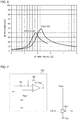
- FIG. 7 is a circuit diagram of a configuration example of the gate voltage adjustment circuit 120 .
- the gate voltage adjustment circuit 120 includes a voltage source 122 and an inverter 124 .
- the internal voltage V REG is supplied to an upper power supply terminal of the inverter 124 and the ground voltage V SS is supplied to a lower power supply terminal.
- the inverter 124 inverts the clock CK supplied to the gate of the PMOS transistor 114 and supplies the inverted clock CK to a gate of the NMOS transistor 112 .
- An output of the inverter 124 is an inversion signal CK# of the clock CK, and a high level thereof is V REG and a low level thereof is V SS .
- FIG. 8A and FIG. 8B are circuit diagrams of a gate voltage adjustment circuit 120 A according to a modification.
- the gate voltage adjustment circuit 120 A in FIG. 8A includes a variable voltage source 126 .
- the variable voltage source 126 adjusts a reference voltage V ADJ so that an on-resistance of a CMOS switch becomes constant.
- FIG. 8B is a circuit diagram illustrating a configuration example of the variable voltage source 126 .
- the variable voltage source 126 includes a dummy switch 128 .
- the dummy switch 128 is a replica of the CMOS switch 110 , and is disposed close to the CMOS switch 110 .
- a high voltage V H (for example, a power supply voltage V DD ) is supplied to a gate of an NMOS transistor, and a low voltage V L (for example, a ground voltage V SS ) is supplied to a gate of a PMOS transistor.
- V H for example, a power supply voltage V DD
- V L for example, a ground voltage V SS
- the dummy switch 128 is connected to a dummy load 129 .
- the variable voltage source 126 outputs the reference voltage V ADJ having a positive correlation with an on-resistance of the dummy switch 128 .
- the reference voltage V ADJ may by generated by inverting and amplifying a voltage V N1 of an output node N 1 of the dummy switch 128 by an inverting amplifier 127 .
- the on-resistance of the CMOS switch 110 fluctuates due to fluctuations in the power supply voltage V DD , process variation, temperature fluctuations, or the like, the on-resistance of the dummy switch 128 fluctuates accordingly, and the reference voltage V ADJ is adjusted.
- the on-resistance of the CMOS switch 110 increases, and the reference voltage V ADJ becomes high.
- an internal voltage V REG becomes high, and the on-resistance of the CMOS switch 110 decreases.
- the on-resistance of the dummy switch 128 decreases and the reference voltage V ADJ becomes low.
- the internal voltage V REG becomes low, and the on-resistance of the CMOS switch 110 increases.
- CMOS switch 110 by monitoring the on-resistance of the CMOS switch 110 using the dummy switch, it is possible to reduce an influence of process variation, fluctuations in a power supply voltage, temperature fluctuations, or the like, and to stabilize the on-resistance of the CMOS switch 110 .
- FIG. 9 is a circuit diagram of a sample hold circuit 100 B in a differential form.
- the sample hold circuit 100 B includes a plurality of CMOS switches 110 A and 110 B and a plurality of capacitors C S1 to C S3 .
- the plurality of CMOS switches 110 A is controlled in accordance with A-phase clocks CKA
- the plurality of CMOS switches 110 B is controlled in accordance with B-phase clocks CKB.
- the A-phase clock CKA and the B-phase clock CKB are in opposite phases.
- a plurality of inverters 124 A and 124 B corresponds to the plurality of CMOS switches 110 A and 110 B.
- the inverter 124 A receives a gate signal CKA of a PMOS transistor 114 of a corresponding CMOS switch 110 A at an input terminal of the inverter 124 A.
- An internal voltage V REG is supplied to a power supply terminal of the inverter 124 A, and an output thereof is connected to the gate of an NMOS transistor 112 of the corresponding CMOS switch 110 A.
- the inverter 124 B receives a gate signal CKB of a PMOS transistor 114 of a corresponding CMOS switch 110 B at an input terminal of the inverter 124 B.
- the internal voltage V REG is supplied to a power supply terminal of the inverter 124 B, and an output thereof is connected to the gate of an NMOS transistor 112 of the corresponding CMOS switch 110 B.
- One inverter 124 A may be provided in common for all the CMOS switches 110 A, or one inverter 124 A may be provided for each CMOS switch 110 A. The same applies to the inverter 124 B.
- One inverter 124 B may be provided in common for all the CMOS switches 110 B, or one inverter 124 B may be provided for each CMOS switch 110 B.
- FIG. 10 is an operation waveform diagram of the sample hold circuit 100 B of FIG. 9 .
- the sample hold circuit 100 B of FIG. 9 power supply voltage dependency of an on-resistance of the CMOS switch can be reduced.
- FIG. 11A is a waveform diagram illustrating the noise characteristics of the sample hold circuit of FIG. 9 .
- FIG. 11B illustrates noise characteristics of a circuit in which a sample hold circuit in related art is configured in a differential form. Note that output voltages in FIG. 11A and FIG. 11B indicate differential components (SHO + ⁇ SHO ⁇ ). As is apparent from comparison between FIG. 11A and FIG. 11B , according to the sample hold circuit 100 B of FIG. 9 , amplitude of a switching noise can be greatly reduced.
- FIG. 12 is a circuit diagram of a sample hold circuit 10 including a CMOS switch 20 .
- the sample hold circuit 10 includes the CMOS switch 20 and a capacitor C S .
- An input voltage V IN is applied to one end of the CMOS switch 20 , and the other end is connected to a high impedance line 12 .
- the high impedance line 12 is connected to the capacitor C S .
- the CMOS switch 20 includes an NMOS transistor and a PMOS transistor connected in parallel.
- Complementary clocks CK and CK# are input to a gate of an NMOS transistor 22 and a gate of a PMOS transistor 24 .
- FIG. 13 is a general layout diagram of the CMOS switch 20 . In FIG. 13 , inter-wire capacitances C L1 to C L6 are illustrated.
- crosstalk via the parasitic capacitances C P1 and C P2 causes voltage fluctuation of the high impedance line 12 and movement of charges of the capacitor C S , which causes noises.
- CMOS switch capable of reducing crosstalk or improving symmetry of a parasitic capacitance
- this CMOS switch can be suitably incorporated in the sample hold circuit described above, a use thereof is not limited to the sample hold circuit.
- FIG. 14 is a layout diagram of a CMOS switch 300 according to the embodiment.
- the CMOS switch 300 includes an NMOS transistor 310 and a PMOS transistor 330 electrically connected in parallel.
- the NMOS transistor 310 and the PMOS transistor 330 are disposed adjacent to each other on a semiconductor substrate in a first direction (an x direction in the drawing). Drains, gates, and sources of the NMOS transistor 310 and the PMOS transistor 330 are disposed in the first direction (or a direction opposite to the first direction). Note that a distinction between a drain D and a source S is made for convenience, and they can be interchanged. In the drawing, filled portions represent contacts.
- Wirings W 1 to W 4 are drawn out from the drain D and the source S of each of the NMOS transistor 310 and the PMOS transistor 330 in a second direction (a y direction in the drawing) orthogonal to the first direction.
- Gates 312 and 332 of the NMOS transistor 310 and the PMOS transistor 330 are extended so as to have a dimension d (referred to as a gate width) longer than a channel width W in a direction opposite to the second direction (a y-axis negative direction in the drawing).
- a gate width referred to as a gate width
- the gate width d and the channel width W are equal, but in the present embodiment, they do not match and d>W.
- the channel width W is defined by widths of a drain region and a source region where impurities are diffused.
- gate lines WG 1 and WG 2 are respectively drawn out from an end of the gate 312 of the NMOS transistor 310 and an end of the gate 332 of the PMOS transistor 330 in the direction opposite to the second direction (the y-axis negative direction).
- a shield line WS is formed so as to cross with the gates 312 and 332 of the NMOS transistor 310 and the PMOS transistor 330 and extend in the first direction (an x-axis direction). That is, the shield line WS blocks electrical coupling between contacts of the drains (D) and the sources (S) and the contacts of the gates (G).
- the shield line WS is grounded, and a potential thereof is fixed.
- FIG. 15 is a cross-sectional view of the CMOS switch 300 of FIG. 14 taken along a line A-A′.
- the shield line WS has a multilayer wiring structure.
- the shield line WS includes a wiring 340 formed in a first layer, a wiring 342 formed in a second layer, and via holes 344 connecting the wirings 340 and 342 .
- CMOS switch 300 The above is the configuration of the CMOS switch 300 . Next, an advantage of the CMOS switch 300 will be described.
- the gates 312 and 332 of the NMOS transistor 310 and the PMOS transistor 330 are extended wider than the channel width W As a result, the contacts of the gates can be moved away from the contacts of the drains (the contacts of the sources) to lengthen a distance between the gate lines WG 1 and WG 2 and the drain/source wirings W 1 to W 4 . With this arrangement, an inter-wire capacitance between the gate lines WG 1 and WG 2 and the drain/source wirings W 1 to W 4 can be reduced, and crosstalk can be suppressed.
- the shield line WS is formed between the gate lines WG 1 and WG 2 and the drain/source wirings W 1 to W 4 in a direction orthogonal to the gate lines WG 1 and WG 2 and the drain/source wirings W 1 to W 4 .
- parasitic capacitances are generated between the drain/source wirings W 1 to W 4 and the shield line WS, instead of between the drain/source wirings W 1 to W 4 and the gate lines.
- coupling between the drain/source wirings W 1 to W 4 and the gate lines WG 1 and WG 2 is weakened and the crosstalk can be further reduced.
- a parasitic capacitance between the drain wiring W 2 and the shield line WS and a parasitic capacitance between the source wiring W 1 and the shield line WS become substantially equal, and imbalance in the parasitic capacitance is also eliminated.
- symmetry of the parasitic capacitances can be maintained.
- the crosstalk between the gate lines and the drain wirings (the source wirings) can be further reduced by multilaying the shield line WS.
- FIG. 16A is a circuit diagram of a sample hold circuit in a differential form including the CMOS switch 300 of FIG. 14
- FIG. 16B is a diagram illustrating a gate clock.
- a sample hold circuit 400 in FIG. 16A includes a plurality of capacitors C S1 to C S3 and a plurality of the CMOS switches 300 .
- the plurality of CMOS switches 300 is driven by complementary gate clocks C and D illustrated in FIG. 16B .
- Each of the plurality of CMOS switches 300 has the layout of FIG. 14 .
- FIG. 17A and FIG. 17B are operation waveform diagrams of the sample hold circuit 400 of FIG. 16A .
- FIG. 17A illustrates an output voltage of the sample hold circuit 400
- FIG. 17B illustrated the gate clock C.
- FIG. 17C illustrates a waveform of an output voltage of a sample hold circuit including the CMOS switch 20 having a layout of FIG. 13 . Note that the output voltage of the sample hold circuit indicates a differential component (SHO + ⁇ SHO ⁇ ).
- the output voltage is constant.
- the output voltage of the sample hold circuit fluctuates with amplitude of ⁇ V ⁇ 2 ⁇ V or so in synchronization with the gate clock.
- CMOS switch 300 of FIG. 14 there is symmetry between the inter-wire capacitance of a drain side and the inter-wire capacitance of a source side. Further, the symmetry can be easily maintained even when the plurality of the CMOS switches 300 of FIG. 14 is arranged. This advantage is particularly suitable for a circuit including a plurality of CMOS switches which is required to have symmetry as in the sample hold circuit 400 of FIG. 16A .
- a shield line WS may be a power supply line to which a bypass capacitor having a large capacitance is connected.
- a gate width d of gates 312 and 332 may be further widened so that two shield wirings WS are formed adjacently in a second direction.
- CMOS switch including an NMOS transistor and a PMOS transistor connected in parallel, in which
- the NMOS transistor and the PMOS transistor are disposed adjacent to each other on a semiconductor substrate in a first direction
- wirings are drawn out from a drain and a source of each of the NMOS transistor and the PMOS transistor in a second direction orthogonal to the first direction,
- a gate of each of the NMOS transistor and the PMOS transistor is extended in a direction opposite to the second direction so as to have a dimension longer than a channel width
- a gate line is drawn out from an end of the gate of each of the NMOS transistor and the PMOS transistor in the direction opposite to the second direction, and
- a shield line crossing with the gate and extending in the first direction is formed.
Abstract
Description
ΔV 1 =C PD/(C OUT +C PD)×V DD (1)
ΔV 2 =C ND/(C OUT +C ND)×V DD (2)
ΔV 3=αP ×Q P /C OUT=αP ×C PB×(V DD −V TP)/C OUT (3)
ΔV 4=αN ×Q N /C OUT=αN ×C NB×(V DD −V TN)/C OUT (4)
V REG <V DD
Claims (10)
Applications Claiming Priority (6)
| Application Number | Priority Date | Filing Date | Title |
|---|---|---|---|
| JP2017-223027 | 2017-11-20 | ||
| JP2017-223026 | 2017-11-20 | ||
| JP2017223027 | 2017-11-20 | ||
| JP2017223026 | 2017-11-20 | ||
| JP2018-194995 | 2018-10-16 | ||
| JP2018194995A JP7262202B2 (en) | 2017-11-20 | 2018-10-16 | semiconductor equipment |
Publications (2)
| Publication Number | Publication Date |
|---|---|
| US20190156906A1 US20190156906A1 (en) | 2019-05-23 |
| US10586605B2 true US10586605B2 (en) | 2020-03-10 |
Family
ID=66533176
Family Applications (1)
| Application Number | Title | Priority Date | Filing Date |
|---|---|---|---|
| US16/194,821 Active US10586605B2 (en) | 2017-11-20 | 2018-11-19 | Sample hold circuit |
Country Status (1)
| Country | Link |
|---|---|
| US (1) | US10586605B2 (en) |
Families Citing this family (3)
| Publication number | Priority date | Publication date | Assignee | Title |
|---|---|---|---|---|
| US11264111B2 (en) | 2017-08-14 | 2022-03-01 | Silicon Laboratories Inc. | Reduced-leakage apparatus for sampling electrical signals and associated methods |
| JP7351156B2 (en) * | 2019-09-18 | 2023-09-27 | セイコーエプソン株式会社 | Circuit devices, electro-optical devices and electronic equipment |
| CN110943726A (en) * | 2019-12-12 | 2020-03-31 | 西安电子科技大学 | Multi-channel multi-stage parallel ultra-high-speed sample hold circuit |
Citations (5)
| Publication number | Priority date | Publication date | Assignee | Title |
|---|---|---|---|---|
| US6636083B1 (en) * | 2001-04-24 | 2003-10-21 | Pacesetter, Inc. | Leakage current cancellation technique for low power switched-capacitor circuits |
| JP2011150561A (en) | 2010-01-22 | 2011-08-04 | Rohm Co Ltd | Semiconductor integrated circuit, differential amplifier using the same, and buffer amplifier |
| US8212604B2 (en) * | 2009-08-07 | 2012-07-03 | Stmicroelectronics Asia Pacific Pte. Ltd. | T switch with high off state isolation |
| US8325257B2 (en) * | 2009-12-11 | 2012-12-04 | Canon Kabushiki Kaisha | Solid-state image pickup device and method for driving the same |
| JP2014171035A (en) | 2013-03-01 | 2014-09-18 | Rohm Co Ltd | Δς a/d converter, audio signal processing circuit and electronic apparatus using the same, and δς modulation method |
Family Cites Families (1)
| Publication number | Priority date | Publication date | Assignee | Title |
|---|---|---|---|---|
| US6963460B2 (en) * | 2002-11-14 | 2005-11-08 | Stmicroelectronics, Inc. | Voltage regulator operable over a wide range of supply voltage |
-
2018
- 2018-11-19 US US16/194,821 patent/US10586605B2/en active Active
Patent Citations (5)
| Publication number | Priority date | Publication date | Assignee | Title |
|---|---|---|---|---|
| US6636083B1 (en) * | 2001-04-24 | 2003-10-21 | Pacesetter, Inc. | Leakage current cancellation technique for low power switched-capacitor circuits |
| US8212604B2 (en) * | 2009-08-07 | 2012-07-03 | Stmicroelectronics Asia Pacific Pte. Ltd. | T switch with high off state isolation |
| US8325257B2 (en) * | 2009-12-11 | 2012-12-04 | Canon Kabushiki Kaisha | Solid-state image pickup device and method for driving the same |
| JP2011150561A (en) | 2010-01-22 | 2011-08-04 | Rohm Co Ltd | Semiconductor integrated circuit, differential amplifier using the same, and buffer amplifier |
| JP2014171035A (en) | 2013-03-01 | 2014-09-18 | Rohm Co Ltd | Δς a/d converter, audio signal processing circuit and electronic apparatus using the same, and δς modulation method |
Also Published As
| Publication number | Publication date |
|---|---|
| US20190156906A1 (en) | 2019-05-23 |
Similar Documents
| Publication | Publication Date | Title |
|---|---|---|
| US7746152B2 (en) | Switch circuit device, and wireless circuit device and sampling circuit device employing the same | |
| US10586605B2 (en) | Sample hold circuit | |
| US9013212B2 (en) | Stress reduced cascoded CMOS output driver circuit | |
| US9667244B1 (en) | Method of and apparatus for biasing switches | |
| US7471111B2 (en) | Slew-rate controlled pad driver in digital CMOS process using parasitic device cap | |
| US8354873B2 (en) | Transmission gate and semiconductor device | |
| JP5018245B2 (en) | Analog switch | |
| US7298201B2 (en) | Clock buffer circuit having predetermined gain with bias circuit thereof | |
| US8378754B2 (en) | Ring oscillator | |
| US10003326B1 (en) | Ring oscillator | |
| US5550503A (en) | Circuits and method for reducing voltage error when charging and discharging a capacitor through a transmission gate | |
| EP0589123B1 (en) | A driver circuit for an electronic switch | |
| JP7262202B2 (en) | semiconductor equipment | |
| US7932764B2 (en) | Delay circuit with constant time delay independent of temperature variations | |
| US20100109774A1 (en) | Operational amplifier | |
| EP4258546A1 (en) | Device for copying a current | |
| US6636073B2 (en) | Semiconductor integrated circuit | |
| US6867629B2 (en) | Integrated circuit and method of adjusting capacitance of a node of an integrated circuit | |
| KR20030072527A (en) | Generator of dc-dc converter | |
| US6566934B1 (en) | Charge cancellation circuit for switched capacitor applications | |
| JPH09261016A (en) | Trapezoidal wave signal output device | |
| JP2009147501A (en) | Semiconductor device | |
| US9838015B2 (en) | Apparatus for performing level shift control in an electronic device with aid of parallel paths controlled by different control signals for current control purposes | |
| US10720924B2 (en) | Adiabatic logic cell | |
| KR100234564B1 (en) | Analogue delay circuit |
Legal Events
| Date | Code | Title | Description |
|---|---|---|---|
| AS | Assignment |
Owner name: ROH, JAPAN Free format text: ASSIGNMENT OF ASSIGNORS INTEREST;ASSIGNORS:NOMURA, NAOHIRO;MANABE, TAKATOSHI;REEL/FRAME:047539/0218 Effective date: 20181113 |
|
| FEPP | Fee payment procedure |
Free format text: ENTITY STATUS SET TO UNDISCOUNTED (ORIGINAL EVENT CODE: BIG.); ENTITY STATUS OF PATENT OWNER: LARGE ENTITY |
|
| AS | Assignment |
Owner name: ROHM CO., LTD., JAPAN Free format text: CORRECTIVE ASSIGNMENT TO CORRECT THE ASSIGNEE'S NAME PREVIOUSLY RECORDED AT REEL: 047539 FRAME: 0218. ASSIGNOR(S) HEREBY CONFIRMS THE ASSIGNMENT;ASSIGNORS:NOMURA, NAOHIRO;MANABE, TAKATOSHI;REEL/FRAME:048172/0865 Effective date: 20181113 |
|
| STPP | Information on status: patent application and granting procedure in general |
Free format text: DOCKETED NEW CASE - READY FOR EXAMINATION |
|
| STPP | Information on status: patent application and granting procedure in general |
Free format text: NON FINAL ACTION MAILED |
|
| STPP | Information on status: patent application and granting procedure in general |
Free format text: RESPONSE TO NON-FINAL OFFICE ACTION ENTERED AND FORWARDED TO EXAMINER |
|
| STPP | Information on status: patent application and granting procedure in general |
Free format text: NOTICE OF ALLOWANCE MAILED -- APPLICATION RECEIVED IN OFFICE OF PUBLICATIONS |
|
| STPP | Information on status: patent application and granting procedure in general |
Free format text: PUBLICATIONS -- ISSUE FEE PAYMENT RECEIVED |
|
| STCF | Information on status: patent grant |
Free format text: PATENTED CASE |
|
| MAFP | Maintenance fee payment |
Free format text: PAYMENT OF MAINTENANCE FEE, 4TH YEAR, LARGE ENTITY (ORIGINAL EVENT CODE: M1551); ENTITY STATUS OF PATENT OWNER: LARGE ENTITY Year of fee payment: 4 |