US10541344B2 - Texturing ribbons for photovoltaic module production - Google Patents
Texturing ribbons for photovoltaic module production Download PDFInfo
- Publication number
- US10541344B2 US10541344B2 US15/540,842 US201615540842A US10541344B2 US 10541344 B2 US10541344 B2 US 10541344B2 US 201615540842 A US201615540842 A US 201615540842A US 10541344 B2 US10541344 B2 US 10541344B2
- Authority
- US
- United States
- Prior art keywords
- module
- cell
- electrodes
- ribbon
- ribbons
- Prior art date
- Legal status (The legal status is an assumption and is not a legal conclusion. Google has not performed a legal analysis and makes no representation as to the accuracy of the status listed.)
- Active, expires
Links
- 238000004519 manufacturing process Methods 0.000 title description 14
- 238000000034 method Methods 0.000 claims abstract description 30
- 230000008878 coupling Effects 0.000 claims abstract description 15
- 238000010168 coupling process Methods 0.000 claims abstract description 15
- 238000005859 coupling reaction Methods 0.000 claims abstract description 15
- 238000005476 soldering Methods 0.000 claims description 28
- 229910052751 metal Inorganic materials 0.000 claims description 19
- 239000002184 metal Substances 0.000 claims description 19
- 229910000679 solder Inorganic materials 0.000 claims description 18
- 230000005496 eutectics Effects 0.000 claims description 5
- 230000006870 function Effects 0.000 description 11
- 239000011521 glass Substances 0.000 description 9
- 230000005611 electricity Effects 0.000 description 8
- 238000002474 experimental method Methods 0.000 description 8
- BQCADISMDOOEFD-UHFFFAOYSA-N Silver Chemical compound [Ag] BQCADISMDOOEFD-UHFFFAOYSA-N 0.000 description 6
- 238000010586 diagram Methods 0.000 description 6
- 229910052709 silver Inorganic materials 0.000 description 6
- 239000004332 silver Substances 0.000 description 6
- 239000010949 copper Substances 0.000 description 5
- 239000000654 additive Substances 0.000 description 4
- 230000000996 additive effect Effects 0.000 description 4
- RYGMFSIKBFXOCR-UHFFFAOYSA-N Copper Chemical compound [Cu] RYGMFSIKBFXOCR-UHFFFAOYSA-N 0.000 description 3
- 239000011248 coating agent Substances 0.000 description 3
- 238000000576 coating method Methods 0.000 description 3
- 229910052802 copper Inorganic materials 0.000 description 3
- 229910021419 crystalline silicon Inorganic materials 0.000 description 3
- 239000000463 material Substances 0.000 description 3
- 239000004065 semiconductor Substances 0.000 description 3
- 229910001174 tin-lead alloy Inorganic materials 0.000 description 3
- PXHVJJICTQNCMI-UHFFFAOYSA-N Nickel Chemical compound [Ni] PXHVJJICTQNCMI-UHFFFAOYSA-N 0.000 description 2
- 229910052782 aluminium Inorganic materials 0.000 description 2
- XAGFODPZIPBFFR-UHFFFAOYSA-N aluminium Chemical compound [Al] XAGFODPZIPBFFR-UHFFFAOYSA-N 0.000 description 2
- 238000003491 array Methods 0.000 description 2
- 230000000694 effects Effects 0.000 description 2
- 239000005340 laminated glass Substances 0.000 description 2
- 238000007650 screen-printing Methods 0.000 description 2
- 238000007711 solidification Methods 0.000 description 2
- 230000008023 solidification Effects 0.000 description 2
- 229920000049 Carbon (fiber) Polymers 0.000 description 1
- ATJFFYVFTNAWJD-UHFFFAOYSA-N Tin Chemical compound [Sn] ATJFFYVFTNAWJD-UHFFFAOYSA-N 0.000 description 1
- RTAQQCXQSZGOHL-UHFFFAOYSA-N Titanium Chemical compound [Ti] RTAQQCXQSZGOHL-UHFFFAOYSA-N 0.000 description 1
- 229910045601 alloy Inorganic materials 0.000 description 1
- 239000000956 alloy Substances 0.000 description 1
- 230000003667 anti-reflective effect Effects 0.000 description 1
- 230000009286 beneficial effect Effects 0.000 description 1
- 239000004917 carbon fiber Substances 0.000 description 1
- 239000004020 conductor Substances 0.000 description 1
- 238000009792 diffusion process Methods 0.000 description 1
- 238000007772 electroless plating Methods 0.000 description 1
- 230000008020 evaporation Effects 0.000 description 1
- 238000001704 evaporation Methods 0.000 description 1
- 239000011152 fibreglass Substances 0.000 description 1
- 239000007769 metal material Substances 0.000 description 1
- VNWKTOKETHGBQD-UHFFFAOYSA-N methane Chemical compound C VNWKTOKETHGBQD-UHFFFAOYSA-N 0.000 description 1
- 229910021421 monocrystalline silicon Inorganic materials 0.000 description 1
- 229910052759 nickel Inorganic materials 0.000 description 1
- 239000004033 plastic Substances 0.000 description 1
- 239000002985 plastic film Substances 0.000 description 1
- 229920006255 plastic film Polymers 0.000 description 1
- 238000007747 plating Methods 0.000 description 1
- 229910021420 polycrystalline silicon Inorganic materials 0.000 description 1
- 238000004544 sputter deposition Methods 0.000 description 1
- 239000010935 stainless steel Substances 0.000 description 1
- 229910001220 stainless steel Inorganic materials 0.000 description 1
- 239000010409 thin film Substances 0.000 description 1
- 229910052718 tin Inorganic materials 0.000 description 1
- 239000010936 titanium Substances 0.000 description 1
- 229910052719 titanium Inorganic materials 0.000 description 1
- 238000007740 vapor deposition Methods 0.000 description 1
Images


Classifications
-
- H—ELECTRICITY
- H01—ELECTRIC ELEMENTS
- H01L—SEMICONDUCTOR DEVICES NOT COVERED BY CLASS H10
- H01L31/00—Semiconductor devices sensitive to infrared radiation, light, electromagnetic radiation of shorter wavelength or corpuscular radiation and specially adapted either for the conversion of the energy of such radiation into electrical energy or for the control of electrical energy by such radiation; Processes or apparatus specially adapted for the manufacture or treatment thereof or of parts thereof; Details thereof
- H01L31/04—Semiconductor devices sensitive to infrared radiation, light, electromagnetic radiation of shorter wavelength or corpuscular radiation and specially adapted either for the conversion of the energy of such radiation into electrical energy or for the control of electrical energy by such radiation; Processes or apparatus specially adapted for the manufacture or treatment thereof or of parts thereof; Details thereof adapted as photovoltaic [PV] conversion devices
- H01L31/042—PV modules or arrays of single PV cells
- H01L31/05—Electrical interconnection means between PV cells inside the PV module, e.g. series connection of PV cells
- H01L31/0504—Electrical interconnection means between PV cells inside the PV module, e.g. series connection of PV cells specially adapted for series or parallel connection of solar cells in a module
- H01L31/0508—Electrical interconnection means between PV cells inside the PV module, e.g. series connection of PV cells specially adapted for series or parallel connection of solar cells in a module the interconnection means having a particular shape
-
- H—ELECTRICITY
- H01—ELECTRIC ELEMENTS
- H01L—SEMICONDUCTOR DEVICES NOT COVERED BY CLASS H10
- H01L24/00—Arrangements for connecting or disconnecting semiconductor or solid-state bodies; Methods or apparatus related thereto
- H01L24/01—Means for bonding being attached to, or being formed on, the surface to be connected, e.g. chip-to-package, die-attach, "first-level" interconnects; Manufacturing methods related thereto
- H01L24/26—Layer connectors, e.g. plate connectors, solder or adhesive layers; Manufacturing methods related thereto
- H01L24/28—Structure, shape, material or disposition of the layer connectors prior to the connecting process
- H01L24/29—Structure, shape, material or disposition of the layer connectors prior to the connecting process of an individual layer connector
-
- H—ELECTRICITY
- H01—ELECTRIC ELEMENTS
- H01L—SEMICONDUCTOR DEVICES NOT COVERED BY CLASS H10
- H01L24/00—Arrangements for connecting or disconnecting semiconductor or solid-state bodies; Methods or apparatus related thereto
- H01L24/80—Methods for connecting semiconductor or other solid state bodies using means for bonding being attached to, or being formed on, the surface to be connected
- H01L24/83—Methods for connecting semiconductor or other solid state bodies using means for bonding being attached to, or being formed on, the surface to be connected using a layer connector
-
- H—ELECTRICITY
- H01—ELECTRIC ELEMENTS
- H01L—SEMICONDUCTOR DEVICES NOT COVERED BY CLASS H10
- H01L31/00—Semiconductor devices sensitive to infrared radiation, light, electromagnetic radiation of shorter wavelength or corpuscular radiation and specially adapted either for the conversion of the energy of such radiation into electrical energy or for the control of electrical energy by such radiation; Processes or apparatus specially adapted for the manufacture or treatment thereof or of parts thereof; Details thereof
- H01L31/04—Semiconductor devices sensitive to infrared radiation, light, electromagnetic radiation of shorter wavelength or corpuscular radiation and specially adapted either for the conversion of the energy of such radiation into electrical energy or for the control of electrical energy by such radiation; Processes or apparatus specially adapted for the manufacture or treatment thereof or of parts thereof; Details thereof adapted as photovoltaic [PV] conversion devices
- H01L31/042—PV modules or arrays of single PV cells
- H01L31/05—Electrical interconnection means between PV cells inside the PV module, e.g. series connection of PV cells
- H01L31/0504—Electrical interconnection means between PV cells inside the PV module, e.g. series connection of PV cells specially adapted for series or parallel connection of solar cells in a module
- H01L31/0512—Electrical interconnection means between PV cells inside the PV module, e.g. series connection of PV cells specially adapted for series or parallel connection of solar cells in a module made of a particular material or composition of materials
-
- H—ELECTRICITY
- H01—ELECTRIC ELEMENTS
- H01L—SEMICONDUCTOR DEVICES NOT COVERED BY CLASS H10
- H01L31/00—Semiconductor devices sensitive to infrared radiation, light, electromagnetic radiation of shorter wavelength or corpuscular radiation and specially adapted either for the conversion of the energy of such radiation into electrical energy or for the control of electrical energy by such radiation; Processes or apparatus specially adapted for the manufacture or treatment thereof or of parts thereof; Details thereof
- H01L31/04—Semiconductor devices sensitive to infrared radiation, light, electromagnetic radiation of shorter wavelength or corpuscular radiation and specially adapted either for the conversion of the energy of such radiation into electrical energy or for the control of electrical energy by such radiation; Processes or apparatus specially adapted for the manufacture or treatment thereof or of parts thereof; Details thereof adapted as photovoltaic [PV] conversion devices
- H01L31/054—Optical elements directly associated or integrated with the PV cell, e.g. light-reflecting means or light-concentrating means
- H01L31/0543—Optical elements directly associated or integrated with the PV cell, e.g. light-reflecting means or light-concentrating means comprising light concentrating means of the refractive type, e.g. lenses
-
- H—ELECTRICITY
- H01—ELECTRIC ELEMENTS
- H01L—SEMICONDUCTOR DEVICES NOT COVERED BY CLASS H10
- H01L31/00—Semiconductor devices sensitive to infrared radiation, light, electromagnetic radiation of shorter wavelength or corpuscular radiation and specially adapted either for the conversion of the energy of such radiation into electrical energy or for the control of electrical energy by such radiation; Processes or apparatus specially adapted for the manufacture or treatment thereof or of parts thereof; Details thereof
- H01L31/04—Semiconductor devices sensitive to infrared radiation, light, electromagnetic radiation of shorter wavelength or corpuscular radiation and specially adapted either for the conversion of the energy of such radiation into electrical energy or for the control of electrical energy by such radiation; Processes or apparatus specially adapted for the manufacture or treatment thereof or of parts thereof; Details thereof adapted as photovoltaic [PV] conversion devices
- H01L31/054—Optical elements directly associated or integrated with the PV cell, e.g. light-reflecting means or light-concentrating means
- H01L31/0547—Optical elements directly associated or integrated with the PV cell, e.g. light-reflecting means or light-concentrating means comprising light concentrating means of the reflecting type, e.g. parabolic mirrors, concentrators using total internal reflection
-
- H—ELECTRICITY
- H01—ELECTRIC ELEMENTS
- H01L—SEMICONDUCTOR DEVICES NOT COVERED BY CLASS H10
- H01L31/00—Semiconductor devices sensitive to infrared radiation, light, electromagnetic radiation of shorter wavelength or corpuscular radiation and specially adapted either for the conversion of the energy of such radiation into electrical energy or for the control of electrical energy by such radiation; Processes or apparatus specially adapted for the manufacture or treatment thereof or of parts thereof; Details thereof
- H01L31/18—Processes or apparatus specially adapted for the manufacture or treatment of these devices or of parts thereof
- H01L31/1876—Particular processes or apparatus for batch treatment of the devices
- H01L31/188—Apparatus specially adapted for automatic interconnection of solar cells in a module
-
- H—ELECTRICITY
- H02—GENERATION; CONVERSION OR DISTRIBUTION OF ELECTRIC POWER
- H02S—GENERATION OF ELECTRIC POWER BY CONVERSION OF INFRARED RADIATION, VISIBLE LIGHT OR ULTRAVIOLET LIGHT, e.g. USING PHOTOVOLTAIC [PV] MODULES
- H02S40/00—Components or accessories in combination with PV modules, not provided for in groups H02S10/00 - H02S30/00
- H02S40/20—Optical components
- H02S40/22—Light-reflecting or light-concentrating means
-
- Y—GENERAL TAGGING OF NEW TECHNOLOGICAL DEVELOPMENTS; GENERAL TAGGING OF CROSS-SECTIONAL TECHNOLOGIES SPANNING OVER SEVERAL SECTIONS OF THE IPC; TECHNICAL SUBJECTS COVERED BY FORMER USPC CROSS-REFERENCE ART COLLECTIONS [XRACs] AND DIGESTS
- Y02—TECHNOLOGIES OR APPLICATIONS FOR MITIGATION OR ADAPTATION AGAINST CLIMATE CHANGE
- Y02E—REDUCTION OF GREENHOUSE GAS [GHG] EMISSIONS, RELATED TO ENERGY GENERATION, TRANSMISSION OR DISTRIBUTION
- Y02E10/00—Energy generation through renewable energy sources
- Y02E10/50—Photovoltaic [PV] energy
- Y02E10/52—PV systems with concentrators
Definitions
- the field of this disclosure relates generally to photovoltaic (PV) systems and, more specifically, to texturing PV module ribbons for PV module production.
- PV photovoltaic
- PV modules are devices which convert solar energy into electricity.
- a PV module includes several PV cells—connected in series and/or in parallel—that generate electricity in response to sunlight (or artificial light) incident on the surface of the cells by the photovoltaic effect.
- electrodes are manufactured on one or both faces of a semiconducting material (e.g., a crystalline silicon wafer) that at least partially forms the light-absorbing structure of the PV cell.
- a semiconducting material e.g., a crystalline silicon wafer
- Various techniques are known for manufacturing PV cell electrodes.
- electrodes include fingers and bus bars, and are screen printed onto a surface of the semiconducting material using silver (Ag) paste.
- Some other techniques include screen printing fingers from silver and soldering separate bus bars to the fingers.
- fingers are screen printed on the semiconducting material using silver.
- PV cells are connected to each other by soldering conductive ribbons to the PV cell electrodes.
- the conductive ribbons electrically couple together the cells within a PV module and are sometimes referred to as tabbing, interconnect, or bus wire.
- An example conductive ribbon includes a copper (Cu) core coated with a tin-lead alloy (60Sn/40Pb) solder metal. These ribbons are soldered to the electrodes (e.g., the bus bars) on the front and back faces of the PV cells. The ribbons cover part of the surface of the cells and block some light from reaching the cell. The fraction of surface area of the cell that is covered up by these ribbons is a measure of the amount of useful light blocked from reaching the photoactive areas of the PV cell. In some cases, these ribbons reduce light incident on the photoactive areas of the PV cell by up to five percent.
- a method for directly imparting a light-capturing texture to a photovoltaic module ribbon on a photovoltaic cell including a plurality of first electrodes on a first side and a plurality of second electrodes on a second side includes coupling a first photovoltaic module ribbon to the plurality of first electrodes. The method also includes positioning the photovoltaic cell on a textured base having a light-capturing texture embodied thereon, where the first photovoltaic module ribbon is substantially contacting the light-capturing texture. The method further includes coupling a second photovoltaic module ribbon to the plurality of second electrodes. The method also includes transferring the light-capturing texture of the textured base to the first ribbon using heat energy released when the second photovoltaic module ribbon is coupled to the plurality of second electrodes.
- FIG. 1 is a perspective view of an example PV module
- FIG. 2 is a cross-sectional view of the PV module shown in FIG. 1 ;
- FIGS. 3A and 3B are schematic diagrams of an example PV cell that may be used to produce the PV module shown in FIG. 1 ;
- FIG. 4 is a diagram of an example system for imparting light-capturing textures to PV module ribbons
- FIG. 5 is another diagram of the system shown in FIG. 4 ;
- FIGS. 6A-6E are photograph of example light-capturing textures generated by the system shown in FIGS. 4 and 5 ;
- FIG. 7 is a photograph of an experiment to determine light scatter for an un-textured PV module ribbon.
- FIG. 8 is a photograph of an experiment to determine light scatter for a textured PV module ribbon.
- PV module ribbons for PV module production and, more specifically, for texturing a PV module ribbon of a PV module by directly imparting a light-capturing texture to a surface of the PV module ribbon during manufacture of the PV module.
- PV photovoltaic
- an example photovoltaic (PV) module includes a plurality of photovoltaic (PV) cells electrically interconnected by one or more PV module ribbon.
- the PV module has a laminate structure including a plurality of layers such as, e.g., glass layers, non-reflective layers, electrical connection layers (e.g., including the one or more PV module ribbon), backing layers, layers including PV cells (e.g., the plurality of PV cells), and/or other suitable layers to enable the PV module to function as described herein.
- the PV module also includes a frame circumscribing the interconnected PV cells and/or other layers for providing structural support and/or protection of the PV module.
- the PV module frame may include elements for securing the PV module to a mounting structure, electrically coupling the PV module to other devices or to ground, coupling the PV module to one or more other PV modules to create a photovoltaic (PV) array, and any other suitable elements.
- PV photovoltaic
- a plurality of PV cells are interconnected by electrically coupling PV module ribbons between electrodes of the plurality of PV cells.
- the PV cells are connected in series to output an additive voltage.
- the PV cells are connected in parallel to output an additive current.
- the plurality of PV cells are connected in both series and parallel according to desired characteristics for output voltage and current.
- the PV cells are interconnected in two steps referred to as tabbing and stringing.
- Tabbing is a process by which segments of PV module ribbon are electrically coupled to each PV cell of the PV module. More specifically, for each PV cell of the PV module, segments of PV module ribbon are electrically coupled (e.g., by soldering) to the electrodes on a surface of the PV cell so that a portion of each segment extends from the PV cell for coupling with adjacent cells.
- Stringing is a process by which tabbed PV cells are interconnected. Tabbed PV cells are reversed and disposed on a base in a desired configuration (e.g., in a row) so that extending portions of the PV module ribbon segments coupled to a first (front) surface of a particular PV cell align with corresponding electrodes on a second (back) surface of an adjacent PV cell. For each tabbed PV cell, the aligned PV module ribbon segments are electrically coupled (e.g., by soldering) to the corresponding electrodes of adjacent cells to create a string of PV cells.
- a light-capturing texture may be directly imparted to at least a portion of the PV module ribbons of the string of PV cells by stringing the tabbed PV cells using a textured base.
- heat energy is released after solidification of the solder metal. At least some of this heat energy may transfer through the PV cell to the solder metal of the PV module ribbons on the first (front) side of the tabbed PV cells.
- the relative solder metal is heated beyond its eutectic temperature. The solder metal reflows into the surface of the textured base and solidifies when cooled below its eutectic temperature.
- a light-capturing texture is imparted to those portions of the PV module ribbons on the first (front) side of the tabbed PV cells that reflow into the surface of the textured base.
- FIG. 1 is a perspective view of an example PV module 100 .
- FIG. 2 is a cross-sectional view of PV module 100 taken along line A-A shown in FIG. 1 .
- PV module 100 includes a laminate 102 and a frame 104 circumscribing laminate 102 .
- PV module 100 may be rectangular, as shown in FIG. 1 , or may be any suitable shape.
- one or more PV module 100 may be arranged to create a PV array (not shown). In creating a PV array, PV module 100 may be shaped according to the particular implementation and/or design of the PV array.
- frame 104 circumscribes PV module 100 and is coupled to PV module 100 .
- Frame 104 facilitates protecting laminate 102 and providing structural support for PV module 100 .
- Frame 104 includes an inner surface 106 proximate to laminate 102 and an outer surface 108 distal to laminate 102 .
- Frame 104 may be constructed using any suitable material such as, e.g., aluminum, rolled or stamped stainless steel, plastic, fiberglass, or carbon fiber.
- frame 104 includes elements for securing PV module 100 to a mounting structure (not shown).
- frame 104 includes elements for electrically coupling PV module 100 to other devices or to ground.
- frame 104 includes elements for coupling PV module 100 to other PV modules for creating a PV array (not shown).
- laminate 102 of PV module 100 includes a top surface 110 and a bottom surface 112 . Edges 114 extend between top surface 110 and bottom surface 108 , and around laminate 102 .
- Laminate 102 has a laminate structure including a plurality of layers 116 . Layers 116 may include, e.g., glass layers, non-reflective layers, electrical connection layers, backing layers, and/or other suitable layers to enable PV module 100 to function as described herein. In some embodiments, laminate 102 of PV module 100 may include more or fewer layers 116 , may have different layers 116 , and/or may have different types of layers 116 .
- At least one of layers 116 of laminate 102 includes a plurality of PV cells (not shown).
- the PV cells function to generate electricity using incident light (e.g., from the sun) at the surface of the cell.
- Each PV cell includes electrodes to facilitate extracting the generated electricity from the PV cell.
- the plurality of PV cells are interconnected by electrically coupling PV module ribbons (not shown) between electrodes of adjacent cells.
- PV module 100 includes a plurality of PV cells interconnected in both a series configuration and a parallel configuration, and PV module 100 is configured to generate a desired output voltage and a desired output current.
- PV module 100 includes a plurality of PV cells interconnected in a series configuration to generate an additive voltage.
- PV module 100 includes a plurality of PV cells interconnected in a parallel configuration to generate an additive current.
- FIGS. 3A and 3B are schematic diagrams of an example PV cell 300 that may be used to produce a PV module such as, e.g., PV module 100 shown in FIGS. 1 and 2 .
- FIG. 3A is a schematic diagram of example PV cell 300 including a view of a back surface 302 of cell 300 .
- FIG. 3B is a schematic diagram of example PV cell 300 including a view of a front surface 304 of cell 300 .
- PV cell 300 includes a photoactive wafer 306 for generating electricity using light incident on the surface (i.e., back surface 302 and/or front surface 304 ) of wafer 306 .
- wafer 306 is a crystalline silicon wafer.
- wafer 306 is a monocrystalline silicon wafer, a polycrystalline silicon wafer, another crystalline silicon wafer, a thin film based wafer, or other suitable wafer to enable PV cell 300 to function as described herein.
- PV cell 300 may be a front diffused emitter or a heterojunction PV cell.
- PV cell 300 may be any other suitable type of PV cell.
- PV cell 300 is a pseudo-square shape.
- PV cell 300 may be any suitable shape for producing PV modules and/or PV arrays in various different shapes.
- PV cell 300 also includes a plurality of finger electrodes 308 manufactured on at least front surface 304 of photoactive wafer 306 .
- Finger electrodes 308 are electrically conductive electrodes coupled to and extending in parallel across the surface of wafer 306 . Finger electrodes 308 conduct electricity generated by PV cell 300 .
- Finger electrodes 308 are manufactured on photoactive wafer 306 by screen printing, electroless plating, electrochemical plating, plasma vapor deposition (PVD), sputtering or evaporation, or otherwise disposing a suitably conductive material on the surface of wafer 306 .
- finger electrodes 308 are silver (Ag) and/or copper (Cu) electrodes.
- finger electrodes 308 are made from any other suitably conductive metal, alloy, and/or non-metallic material including, e.g., aluminum, nickel, tin, and/or titanium. In yet other embodiments, finger electrodes 308 are made from any electrically conductive, suitably low resistance, and suitably inexpensive material, and may be made from a material that includes no silver (Ag) or is substantially silver free.
- PV cell 300 includes a plurality of bus electrodes 310 manufactured on back surface 302 of photoactive wafer 306 .
- Bus electrodes 310 are electrically conductive electrodes coupled to and extending in parallel across the surface of wafer 306 .
- bus electrodes 310 are coupled to and extend perpendicular to finger electrodes 308 .
- PV cell 300 includes nine bus electrodes 310 arranged in three groups, where bus electrodes 310 for each group are aligned longitudinally across photoactive wafer 306 and are sometimes referred to as a segmented bus bar.
- PV cell 300 may include fewer or more bus electrodes 310 , and bus electrodes 310 may be any suitable size and/or shape to enable PV cell 300 to function as described herein.
- PV cell 300 also includes a plurality of PV module ribbons 312 coupled to back surface 302 of photoactive wafer 306 .
- PV module ribbons 312 are coupled to bus electrodes 310 and extend across each longitudinally aligned group of bus electrodes 310 .
- PV module ribbons 312 may be coupled to photoactive wafer 306 by finger electrodes 308 in addition to, or in alternative to, bus electrodes 310 .
- PV module ribbons 312 include a conductive core (not shown) covered by a tin-lead alloy solder metal. Alternatively, the conductive core may be covered by any suitable solder metal to enable PV module ribbons 312 to function as described herein.
- PV cell 300 includes a plurality of PV module ribbons 314 coupled to front surface 304 of photoactive wafer 306 .
- PV module ribbons 314 are coupled to finger electrodes 308 and extend longitudinally across photoactive wafer 306 and transverse across finger electrodes 308 .
- PV module ribbons 314 include a conductive core (not shown) covered by a tin-lead alloy solder metal.
- the conductive core may be covered by any suitable solder metal to enable PV module ribbons 314 to function as described herein.
- one or more PV cell 300 are interconnected by soldering PV module ribbons 312 and 314 between adjacent electrodes on back surface 302 and front surface 304 , respectively.
- one or more PV cell 300 are interconnected by soldering PV module ribbons 312 between bus electrodes 310 of adjacent cells (not shown) and soldering PV module ribbons 314 between finger electrodes 308 of adjacent cells to form a string of PV cells (not shown).
- one or more PV cell 300 , or one or more string of PV cells are interconnected by soldering PV module ribbons 312 and 314 between other electrodes, e.g., around the perimeter of laminate 102 (shown in FIGS. 1 and 2 ).
- PV module ribbons 312 and 314 are soldered to electrodes on the opposite surface of adjacent PV cells. More specifically, PV module ribbons 312 are coupled between electrodes 310 on back surface 302 of PV cell 300 and electrodes on the front surface of a first adjacent PV cell (not shown), and PV module ribbons 314 are coupled between electrodes 308 on front surface 304 of PV cell 300 and electrodes on the back surface of a second adjacent PV cell (not shown).
- PV module ribbons 312 and/or 314 at least partially obscure the photoactive areas of PV cell 300 . In some cases, this may reduce the amount of incident light on the photoactive areas by up to about 5%.
- the surface of PV module ribbons 312 and/or 314 is reflective, incoming light is reflected off the surface of the ribbons and away from PV cell 300 . Some of the light reflected off the surface of PV module ribbons 312 and/or 314 may be reflected back to the photoactive areas of PV cell 300 by other layers 116 of laminate 102 (both shown in FIG. 2 ). The amount of light reflected back to photoactive areas of PV cell 300 may be increased by texturing the surface of PV module ribbons 312 and/or 314 .
- a light-capturing texture may result in the diffusion of incoming light reflected by the surface. At least some of the diffused, reflected light leaves the light-capturing surface at a reduced angle relative to the cell's surface, increasing the likelihood that subsequent reflections will occur and the light will reach the photoactive areas of the cell.
- FIGS. 4 and 5 illustrate an example system 400 including a textured base 402 for imparting a light-capturing texture 404 to a PV module ribbon of a PV cell (e.g., PV module ribbons 312 and/or 314 of PV cell 300 ) using textured base 402 .
- FIG. 4 includes textured base 402 and PV cell 300 , where PV cell 300 is positioned adjacent to textured base 402 at front surface 304 and PV module ribbons 314 of PV cell 300 are substantially contacting textured base 402 .
- FIG. 5 includes light-capturing texture 404 imparted to at least a portion 406 of PV module ribbon 314 by textured base 402 .
- system 400 enables producing a PV module (not shown) including PV cell 300 and imparting light-capturing texture 404 to portion 406 of PV module ribbon 314 by textured base 402 during manufacture of the PV module.
- Textured base 402 is shown as triangular and/or pyramid shaped, and may be any other shape to enable system 400 to function as described herein.
- textured base 402 may have any shape that will reflect light normal to the direction of the ribbon 314 , rather than along the length of the ribbon 314 .
- PV module ribbons 314 (sometimes referred to as tabbing ribbons) are electrically coupled to electrodes 308 (shown in FIG.
- PV module ribbons 312 (sometimes referred to as stringing ribbons) are positioned across bus electrodes 310 on back surface 302 of PV cell 300 and are ready to be coupled (e.g., soldered) to bus electrodes 310 to manufacture the PV module.
- soldering PV module ribbons 312 to bus electrodes 310 on back surface 302 directly imparts light-capturing texture 404 to portion 406 of PV module ribbon 314 on front surface 304 .
- PV module ribbons 314 are electrically coupled to PV cell 300 in a process sometimes referred to as tabbing. More specifically, PV module ribbons 314 are soldered to electrodes 308 (shown in FIG. 3 ) on front surface 304 of PV cell 300 . In a process sometimes referred to as stringing, PV cell 300 is positioned so that front surface 304 is facing textured base 402 , and PV module ribbons 314 are substantially contacting textured base 402 . PV module ribbons 312 are positioned across bus electrodes 310 on back surface 302 of PV cell 300 . PV module ribbons 312 are electrically coupled with PV cell 300 by soldering ribbons 312 to bus electrodes 310 .
- heat energy is applied to melt the solder metal coating of ribbons 312 .
- the applied heat energy is removed and the solder metal coating of ribbons 312 cools and solidifies.
- heat energy is released by the solder metal coating after solidification. At least some of the released heat energy transfers across PV cell 300 in areas covered by bus electrodes 310 , from PV module ribbons 312 on back surface 302 to PV module ribbons 314 on front surface 304 .
- the relative solder metal is heated beyond its eutectic temperature.
- the relative solder metal of PV module ribbons 314 reflows into the surface of textured base 402 and solidifies when cooled below its eutectic temperature.
- a relief of textured base 402 is imparted to PV module ribbons 314 when cooled.
- light-capturing texture 404 is imparted to PV module ribbons 314 as the relief of textured base 402 .
- light-capturing texture 404 is imparted to at least portion 406 of PV module ribbons 314 .
- FIGS. 6A-6E are photographic illustrations of example light-capturing textures 600 generated by a system for directly imparting light-capturing textures using a textured base, such as system 400 and textured base 402 (both shown in FIGS. 4 and 5 ).
- Example light-capturing textures 600 are imparted to PV module ribbons 602 during production of relative PV modules (not shown). More specifically, example light-capturing textures 600 are imparted to the surface of PV module ribbons 602 contacting textured base 402 when soldering other PV module ribbons (not shown) on the opposing side of a PV cell 604 .
- PV cell 604 is similar to PV cell 300 shown in FIG. 3 . In other embodiments, PV cell 604 may be any suitable PV cell to enable system 400 to function as described herein.
- light-capturing textures 600 include an inverted pyramid texture 606 as shown in FIGS. 4 and 5 .
- Textured base 402 is a laminated glass having inverted pyramid texture 606 on a surface (not shown) of the glass.
- Inverted pyramid texture 606 is imparted to PV module ribbon 602 when soldering ribbons on the reverse side of PV cell 604 using the laminated glass base.
- inverted pyramid texture 606 is imparted to the portion of PV module ribbon 602 that is positioned on the front surface of PV cell 604 and opposite of bus electrodes (not shown) on the back surface of PV cell 604 .
- light-capturing textures 600 include a matte texture 608 .
- Textured base 402 is a non-anti-reflective coated glass having matte texture 608 on a surface (not shown) of the glass. Matte texture 608 is imparted to PV module ribbon 602 when soldering ribbons on the reverse side of PV cell 604 using the coated glass base. Moreover, matte texture 608 is imparted to the portion of PV module ribbon 602 that is positioned on the front surface of PV cell 604 and opposite of bus electrodes (not shown) on the back surface of PV cell 604 .
- light-capturing textures 600 include a smooth texture 610 .
- Textured base 402 is an un-textured glass having smooth texture 610 on a surface (not shown) of the glass. Smooth texture 610 is imparted to PV module ribbon 602 when soldering ribbons on the reverse side of PV cell 604 using the glass base. Moreover, smooth texture 610 is imparted to the portion of PV module ribbon 602 that is positioned on the front surface of PV cell 604 and opposite of bus electrodes (not shown) on the back surface of PV cell 604 .
- light-capturing textures 600 include an uneven texture 612 .
- Textured base 402 is a soldering fixture having uneven texture 612 on a surface (not shown) of the fixture.
- Uneven texture 612 is imparted to PV module ribbon 602 when soldering ribbons on the reverse side of PV cell 604 using the soldering fixture.
- uneven texture 612 is imparted to the portion of PV module ribbon 602 that is positioned on the front surface of PV cell 604 and opposite of bus electrodes (not shown) on the back surface of PV cell 604 .
- light-capturing textures 600 include a patterned texture 614 .
- Textured base 402 is a component of a cell stringing device (not shown) having patterned texture 614 on a surface (not shown) of the device.
- Patterned texture 614 is imparted to PV module ribbon 602 when soldering ribbons on the reverse side of PV cell 604 using the cell stringing device.
- patterned texture 614 is imparted to the portion of PV module ribbon 602 that is positioned on the front surface of PV cell 604 and opposite of bus electrodes (not shown) on the back surface of PV cell 604 .
- the cell stringing device includes pins for soldering ribbons. Patterned texture 614 is substantially uniform over those portions of PV module ribbon 602 except at a position 616 where one of the pins makes contact during soldering.
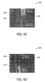
- FIGS. 7 and 8 are photographic illustrations of experiments to determine light scatter for PV module ribbons based on the texture of the PV module ribbon.
- FIG. 7 includes a system 700 including light scatter for an un-textured PV module ribbon 702 .
- FIG. 8 includes a system 800 including light scatter of a textured PV module ribbon 802 generated using a textured base (not shown) such as, e.g., textured base 402 shown in FIGS. 4 and 5 .
- the experiments illustrate enhanced light scatter for PV module ribbons textured during production of PV modules.
- a device is used to illuminate the PV module ribbons and the resulting light scatter is observed.
- the resulting light scatter is quantified by measuring the width of light scatter on the surface of the PV cell.
- system 700 includes an un-textured PV module ribbon 702 coupled with a PV cell 704 .
- PV cell 704 is similar to PV cell 300 shown in FIG. 3 .
- PV cell 704 may be any suitable PV cell to enable system 700 to function as described herein.
- PV cell 704 is electrically coupled with other PV cells (not shown) by soldering PV module ribbon between the cells.
- Un-textured PV module ribbon 702 is generated when soldering relative PV module ribbon (not shown) on the reverse side of PV cell 704 when producing the PV module.
- the experiment shows that a light scatter 706 for un-textured PV module ribbon 702 is substantially zero (i.e., there is very little to no light scatter for un-textured PV module ribbon).
- system 800 includes a textured PV module ribbon 802 generated using a textured base (not shown) and coupled with a PV cell 804 .
- PV cell 804 is similar to PV cell 300 shown in FIG. 3 .
- PV cell 804 may be any suitable PV cell to enable system 800 to function as described herein.
- PV cell 804 is electrically coupled with other PV cells (not shown) by soldering PV module ribbon between the cells.
- Textured PV module ribbon 802 is generated when soldering relative PV module ribbon (not shown) on the reverse side of PV cell 804 when producing the PV module.
- the experiment shows that a light scatter 806 for textured PV module ribbon 802 is about 20 mm.
- Textured PV module ribbons such as, e.g., textured PV module ribbon 802 , include light-capturing textured directly imparted when producing PV modules. The overall efficiency of PV cells, PV modules, and/or PV arrays manufactured with the light-capturing texture is enhanced while the cost and/or complexity of producing them are substantially maintained.
- the example methods and systems described herein produce solar cells with textured solar module ribbons.
- the resulting cells are able to capture light more efficiently than cells with untextured ribbons.
- Solar modules having cells produced as described herein capture more have a greater amount of light incident on the surface of the cells and produce more electricity than modules with untextured ribbons.
- the example methods and systems produce solar cells with textured ribbons without adding any significant extra effort or cost over the cost of producing solar cells without textured ribbons.
Landscapes
- Engineering & Computer Science (AREA)
- Power Engineering (AREA)
- Computer Hardware Design (AREA)
- Microelectronics & Electronic Packaging (AREA)
- Physics & Mathematics (AREA)
- Condensed Matter Physics & Semiconductors (AREA)
- Electromagnetism (AREA)
- General Physics & Mathematics (AREA)
- Sustainable Development (AREA)
- Life Sciences & Earth Sciences (AREA)
- Sustainable Energy (AREA)
- Manufacturing & Machinery (AREA)
- Photovoltaic Devices (AREA)
Priority Applications (1)
| Application Number | Priority Date | Filing Date | Title |
|---|---|---|---|
| US15/540,842 US10541344B2 (en) | 2015-01-06 | 2016-01-05 | Texturing ribbons for photovoltaic module production |
Applications Claiming Priority (3)
| Application Number | Priority Date | Filing Date | Title |
|---|---|---|---|
| US201562100274P | 2015-01-06 | 2015-01-06 | |
| PCT/US2016/012214 WO2016112029A1 (en) | 2015-01-06 | 2016-01-05 | Texturing ribbons for photovoltaic module production |
| US15/540,842 US10541344B2 (en) | 2015-01-06 | 2016-01-05 | Texturing ribbons for photovoltaic module production |
Publications (2)
| Publication Number | Publication Date |
|---|---|
| US20180026151A1 US20180026151A1 (en) | 2018-01-25 |
| US10541344B2 true US10541344B2 (en) | 2020-01-21 |
Family
ID=55272629
Family Applications (1)
| Application Number | Title | Priority Date | Filing Date |
|---|---|---|---|
| US15/540,842 Active 2036-03-03 US10541344B2 (en) | 2015-01-06 | 2016-01-05 | Texturing ribbons for photovoltaic module production |
Country Status (3)
| Country | Link |
|---|---|
| US (1) | US10541344B2 (zh) |
| CN (1) | CN107534068B (zh) |
| WO (1) | WO2016112029A1 (zh) |
Citations (9)
| Publication number | Priority date | Publication date | Assignee | Title |
|---|---|---|---|---|
| US5411897A (en) * | 1994-02-04 | 1995-05-02 | Mobil Solar Energy Corporation | Machine and method for applying solder paste to electronic devices such as solar cells |
| US5998729A (en) * | 1997-04-11 | 1999-12-07 | Canon Kabushiki Kaisha | Solar cell module having improved flexibility |
| US20090277491A1 (en) * | 2005-10-14 | 2009-11-12 | Sharp Kabushiki Kaisha | Solar Cell, Interconnector-Equipped Solar Cell, Solar Cell String And Solar Cell Module |
| US20110271996A1 (en) | 2010-05-04 | 2011-11-10 | Solarworld Innovations Gmbh | Method for fixing a photovoltaic cell connector on a surface of a photovoltaic cell, photovoltaic cell connector forming die, device for fixing a photovoltaic cell connector on a surface of a photovoltaic cell |
| US20130048047A1 (en) | 2010-09-07 | 2013-02-28 | Sony Chemical & Information Device Corporation | Process for manufacture of solar battery module, solar battery cell connection device, and solar battery module |
| US20140048306A1 (en) * | 2012-08-14 | 2014-02-20 | Au Optronics Corporation | Apparatus for Patterning Ribbon, String Tabbing Method and Solar Cell Module Using the Same |
| US20140144481A1 (en) * | 2010-10-14 | 2014-05-29 | Hitachi Chemical Company, Ltd. | Solar cell module |
| US20150004740A1 (en) * | 2012-01-10 | 2015-01-01 | Gens Engineering Co. Ltd | Silicon solar cell module using conductive npaste as electrode and method for manufacturing same |
| US9515200B2 (en) * | 2006-01-24 | 2016-12-06 | Panasonic Intellectual Property Management Co., Ltd. | Photovoltaic module |
Family Cites Families (3)
| Publication number | Priority date | Publication date | Assignee | Title |
|---|---|---|---|---|
| EP2657981A4 (en) * | 2011-01-31 | 2014-02-26 | Sanyo Electric Co | PHOTOELECTRIC TRANSFORMER AND PHOTOELECTRIC CONVERSION MODULE |
| FR2977718B1 (fr) * | 2011-07-07 | 2013-07-12 | Commissariat Energie Atomique | Module photovoltaique a conducteurs sous forme de rubans |
| CN103681911B (zh) * | 2013-12-31 | 2017-02-01 | 赛维Ldk太阳能高科技(南昌)有限公司 | 一种光伏组件 |
-
2016
- 2016-01-05 CN CN201680005009.9A patent/CN107534068B/zh active Active
- 2016-01-05 US US15/540,842 patent/US10541344B2/en active Active
- 2016-01-05 WO PCT/US2016/012214 patent/WO2016112029A1/en active Application Filing
Patent Citations (10)
| Publication number | Priority date | Publication date | Assignee | Title |
|---|---|---|---|---|
| US5411897A (en) * | 1994-02-04 | 1995-05-02 | Mobil Solar Energy Corporation | Machine and method for applying solder paste to electronic devices such as solar cells |
| US5998729A (en) * | 1997-04-11 | 1999-12-07 | Canon Kabushiki Kaisha | Solar cell module having improved flexibility |
| US20090277491A1 (en) * | 2005-10-14 | 2009-11-12 | Sharp Kabushiki Kaisha | Solar Cell, Interconnector-Equipped Solar Cell, Solar Cell String And Solar Cell Module |
| US9515200B2 (en) * | 2006-01-24 | 2016-12-06 | Panasonic Intellectual Property Management Co., Ltd. | Photovoltaic module |
| US20110271996A1 (en) | 2010-05-04 | 2011-11-10 | Solarworld Innovations Gmbh | Method for fixing a photovoltaic cell connector on a surface of a photovoltaic cell, photovoltaic cell connector forming die, device for fixing a photovoltaic cell connector on a surface of a photovoltaic cell |
| US20130048047A1 (en) | 2010-09-07 | 2013-02-28 | Sony Chemical & Information Device Corporation | Process for manufacture of solar battery module, solar battery cell connection device, and solar battery module |
| US20140144481A1 (en) * | 2010-10-14 | 2014-05-29 | Hitachi Chemical Company, Ltd. | Solar cell module |
| US20150004740A1 (en) * | 2012-01-10 | 2015-01-01 | Gens Engineering Co. Ltd | Silicon solar cell module using conductive npaste as electrode and method for manufacturing same |
| US9349882B2 (en) * | 2012-01-10 | 2016-05-24 | Gens Engineering Co. Ltd | Silicon solar cell module using conductive npaste as electrode and method for manufacturing same |
| US20140048306A1 (en) * | 2012-08-14 | 2014-02-20 | Au Optronics Corporation | Apparatus for Patterning Ribbon, String Tabbing Method and Solar Cell Module Using the Same |
Non-Patent Citations (1)
| Title |
|---|
| International Search Report and Written Opinion of the International Search Authority regarding PCT/US2016/012214 dated Apr. 21, 2016; pp. 1-11. |
Also Published As
| Publication number | Publication date |
|---|---|
| WO2016112029A1 (en) | 2016-07-14 |
| CN107534068B (zh) | 2020-08-04 |
| CN107534068A (zh) | 2018-01-02 |
| US20180026151A1 (en) | 2018-01-25 |
Similar Documents
| Publication | Publication Date | Title |
|---|---|---|
| CN104272475B (zh) | 背接触太阳能光伏模块用半导体晶片的电池和模块加工 | |
| JP5159725B2 (ja) | 太陽電池ストリング及びそれを用いた太陽電池モジュール | |
| EP2348539B1 (en) | Photovoltaic cell electrode and method for electrically connecting a photovoltaic cell | |
| KR101890324B1 (ko) | 태양 전지 모듈 및 이에 적용되는 리본 결합체 | |
| CN106653912B (zh) | 一种无栅线全背接触太阳能电池组件 | |
| US20180083152A1 (en) | Crystalline silicon solar cell module and manufacturing method for same | |
| JP6280692B2 (ja) | 太陽電池モジュール、及び結晶系太陽電池モジュールの製造方法 | |
| TWI458104B (zh) | 太陽能電池模組 | |
| JP6368714B2 (ja) | 線状リボン型コネクタストリップを使用した背面接触太陽電池モジュールの製造方法及び各太陽電池モジュール | |
| TW201444103A (zh) | 具有特定電極架構之光伏電池元件 | |
| JP2008159895A (ja) | 太陽電池セル及び太陽電池モジュール | |
| US20120279546A1 (en) | Solar cell connector electrode, solar cell module and method for electrically connecting a plurality of solar cells | |
| JP2007273857A (ja) | 太陽電池セル接続用配線部材およびそれを用いた太陽電池装置 | |
| CN102651407B (zh) | 太阳电池、太阳电池模块以及制备太阳电池的方法 | |
| KR20170063663A (ko) | 특정 전방 표면 전극 디자인을 갖는 태양 전지 | |
| US20120318351A1 (en) | Solar cell having a special busbar shape, solar cell arrangement containing said solar cell, and method for producing the solar cell | |
| Geissbühler et al. | Metallization techniques and interconnection schemes for high efficiency silicon heterojunction PV | |
| TW201607053A (zh) | 具有耦合之展成金屬物件的光伏電池 | |
| US10665744B2 (en) | Bifacial photovoltaic module | |
| TWI502756B (zh) | 具有粗細匯流排電極之太陽能電池 | |
| JP4593980B2 (ja) | 光電変換装置とこれを用いた太陽電池素子、並びに太陽電池モジュール | |
| US10541344B2 (en) | Texturing ribbons for photovoltaic module production | |
| WO2012128284A1 (ja) | 裏面電極型太陽電池、裏面電極型太陽電池の製造方法及び太陽電池モジュール | |
| CN112838135B (zh) | 一种边缘钝化修复的柔性太阳能电池的制备方法 | |
| TWI509816B (zh) | 具有寬窄電極區塊之太陽能電池及使用其之太陽能電池模組 |
Legal Events
| Date | Code | Title | Description |
|---|---|---|---|
| AS | Assignment |
Owner name: CORNER STAR LIMITED, HONG KONG Free format text: ASSIGNMENT OF ASSIGNORS INTEREST;ASSIGNORS:KOPPIKAR, SANDEEP RAMMOHAN;DESHPANDE, ADITYA JANARDAN;CHAUDHARI, VIKRANT ASHOK;AND OTHERS;SIGNING DATES FROM 20170902 TO 20170923;REEL/FRAME:043711/0609 |
|
| AS | Assignment |
Owner name: GCL SYSTEM INTEGRATION TECHNOLOGY (HONG KONG) LIMITED, HONG KONG Free format text: PATENT ACQUISITION AGREEMENT;ASSIGNOR:CORNER STAR LIMITED;REEL/FRAME:047905/0583 Effective date: 20181024 Owner name: GCL SYSTEM INTEGRATION TECHNOLOGY (HONG KONG) LIMI Free format text: PATENT ACQUISITION AGREEMENT;ASSIGNOR:CORNER STAR LIMITED;REEL/FRAME:047905/0583 Effective date: 20181024 |
|
| STPP | Information on status: patent application and granting procedure in general |
Free format text: NON FINAL ACTION MAILED |
|
| STPP | Information on status: patent application and granting procedure in general |
Free format text: RESPONSE TO NON-FINAL OFFICE ACTION ENTERED AND FORWARDED TO EXAMINER |
|
| STPP | Information on status: patent application and granting procedure in general |
Free format text: NOTICE OF ALLOWANCE MAILED -- APPLICATION RECEIVED IN OFFICE OF PUBLICATIONS |
|
| STPP | Information on status: patent application and granting procedure in general |
Free format text: PUBLICATIONS -- ISSUE FEE PAYMENT VERIFIED |
|
| STCF | Information on status: patent grant |
Free format text: PATENTED CASE |
|
| MAFP | Maintenance fee payment |
Free format text: PAYMENT OF MAINTENANCE FEE, 4TH YEAR, LARGE ENTITY (ORIGINAL EVENT CODE: M1551); ENTITY STATUS OF PATENT OWNER: LARGE ENTITY Year of fee payment: 4 |