US10490448B2 - Method of using a sacrificial conductive stack to prevent corrosion - Google Patents
Method of using a sacrificial conductive stack to prevent corrosion Download PDFInfo
- Publication number
- US10490448B2 US10490448B2 US15/858,145 US201715858145A US10490448B2 US 10490448 B2 US10490448 B2 US 10490448B2 US 201715858145 A US201715858145 A US 201715858145A US 10490448 B2 US10490448 B2 US 10490448B2
- Authority
- US
- United States
- Prior art keywords
- conductive stack
- metallization layer
- layer
- window
- recited
- Prior art date
- Legal status (The legal status is an assumption and is not a legal conclusion. Google has not performed a legal analysis and makes no representation as to the accuracy of the status listed.)
- Active
Links
- 238000000034 method Methods 0.000 title claims abstract description 94
- 238000005260 corrosion Methods 0.000 title description 21
- 230000007797 corrosion Effects 0.000 title description 21
- 238000001465 metallisation Methods 0.000 claims abstract description 113
- RYGMFSIKBFXOCR-UHFFFAOYSA-N Copper Chemical compound [Cu] RYGMFSIKBFXOCR-UHFFFAOYSA-N 0.000 claims abstract description 98
- 229910052802 copper Inorganic materials 0.000 claims abstract description 98
- 239000010949 copper Substances 0.000 claims abstract description 98
- 230000004888 barrier function Effects 0.000 claims abstract description 51
- 238000002161 passivation Methods 0.000 claims abstract description 20
- 238000000151 deposition Methods 0.000 claims abstract description 12
- 238000004519 manufacturing process Methods 0.000 claims abstract description 9
- 239000004065 semiconductor Substances 0.000 claims abstract description 9
- 230000008569 process Effects 0.000 claims description 42
- 230000001681 protective effect Effects 0.000 claims description 29
- MZLGASXMSKOWSE-UHFFFAOYSA-N tantalum nitride Chemical compound [Ta]#N MZLGASXMSKOWSE-UHFFFAOYSA-N 0.000 claims description 19
- 229910052751 metal Inorganic materials 0.000 claims description 18
- 239000002184 metal Substances 0.000 claims description 18
- 238000005530 etching Methods 0.000 claims description 17
- KDLHZDBZIXYQEI-UHFFFAOYSA-N Palladium Chemical compound [Pd] KDLHZDBZIXYQEI-UHFFFAOYSA-N 0.000 claims description 13
- PXHVJJICTQNCMI-UHFFFAOYSA-N Nickel Chemical compound [Ni] PXHVJJICTQNCMI-UHFFFAOYSA-N 0.000 claims description 8
- 229910052763 palladium Inorganic materials 0.000 claims description 6
- BASFCYQUMIYNBI-UHFFFAOYSA-N platinum Chemical compound [Pt] BASFCYQUMIYNBI-UHFFFAOYSA-N 0.000 claims description 6
- 238000000992 sputter etching Methods 0.000 claims description 5
- PCHJSUWPFVWCPO-UHFFFAOYSA-N gold Chemical compound [Au] PCHJSUWPFVWCPO-UHFFFAOYSA-N 0.000 claims description 3
- 229910052737 gold Inorganic materials 0.000 claims description 3
- 239000010931 gold Substances 0.000 claims description 3
- 238000007747 plating Methods 0.000 claims description 3
- 229910052697 platinum Inorganic materials 0.000 claims description 3
- 238000005498 polishing Methods 0.000 claims description 3
- 238000001039 wet etching Methods 0.000 claims description 3
- KJTLSVCANCCWHF-UHFFFAOYSA-N Ruthenium Chemical compound [Ru] KJTLSVCANCCWHF-UHFFFAOYSA-N 0.000 claims description 2
- 229910052759 nickel Inorganic materials 0.000 claims description 2
- 229910052707 ruthenium Inorganic materials 0.000 claims description 2
- WFKWXMTUELFFGS-UHFFFAOYSA-N tungsten Chemical compound [W] WFKWXMTUELFFGS-UHFFFAOYSA-N 0.000 claims description 2
- 229910052721 tungsten Inorganic materials 0.000 claims description 2
- 239000010937 tungsten Substances 0.000 claims description 2
- 239000010410 layer Substances 0.000 description 138
- 235000012431 wafers Nutrition 0.000 description 23
- XAGFODPZIPBFFR-UHFFFAOYSA-N aluminium Chemical compound [Al] XAGFODPZIPBFFR-UHFFFAOYSA-N 0.000 description 17
- 229910052782 aluminium Inorganic materials 0.000 description 14
- 239000004642 Polyimide Substances 0.000 description 9
- 229920001721 polyimide Polymers 0.000 description 9
- 230000015654 memory Effects 0.000 description 7
- VYPSYNLAJGMNEJ-UHFFFAOYSA-N Silicium dioxide Chemical compound O=[Si]=O VYPSYNLAJGMNEJ-UHFFFAOYSA-N 0.000 description 6
- 238000003491 array Methods 0.000 description 6
- 230000008878 coupling Effects 0.000 description 5
- 238000010168 coupling process Methods 0.000 description 5
- 238000005859 coupling reaction Methods 0.000 description 5
- 230000015572 biosynthetic process Effects 0.000 description 4
- 238000004140 cleaning Methods 0.000 description 3
- 229920002120 photoresistant polymer Polymers 0.000 description 3
- 239000000523 sample Substances 0.000 description 3
- 229910052581 Si3N4 Inorganic materials 0.000 description 2
- 239000004020 conductor Substances 0.000 description 2
- 239000000356 contaminant Substances 0.000 description 2
- 238000005536 corrosion prevention Methods 0.000 description 2
- 230000008021 deposition Effects 0.000 description 2
- 230000000694 effects Effects 0.000 description 2
- 239000000463 material Substances 0.000 description 2
- 150000002739 metals Chemical class 0.000 description 2
- 150000004767 nitrides Chemical class 0.000 description 2
- 230000003647 oxidation Effects 0.000 description 2
- 238000007254 oxidation reaction Methods 0.000 description 2
- 238000004806 packaging method and process Methods 0.000 description 2
- 238000000059 patterning Methods 0.000 description 2
- 235000012239 silicon dioxide Nutrition 0.000 description 2
- 239000000377 silicon dioxide Substances 0.000 description 2
- HQVNEWCFYHHQES-UHFFFAOYSA-N silicon nitride Chemical compound N12[Si]34N5[Si]62N3[Si]51N64 HQVNEWCFYHHQES-UHFFFAOYSA-N 0.000 description 2
- 229910052814 silicon oxide Inorganic materials 0.000 description 2
- 239000002356 single layer Substances 0.000 description 2
- 229910000679 solder Inorganic materials 0.000 description 2
- 239000000758 substrate Substances 0.000 description 2
- 238000012360 testing method Methods 0.000 description 2
- VYZAMTAEIAYCRO-UHFFFAOYSA-N Chromium Chemical compound [Cr] VYZAMTAEIAYCRO-UHFFFAOYSA-N 0.000 description 1
- 230000004075 alteration Effects 0.000 description 1
- 239000003990 capacitor Substances 0.000 description 1
- 229910052804 chromium Inorganic materials 0.000 description 1
- 239000011651 chromium Substances 0.000 description 1
- 230000001934 delay Effects 0.000 description 1
- 238000013461 design Methods 0.000 description 1
- 238000010586 diagram Methods 0.000 description 1
- -1 e.g. Substances 0.000 description 1
- 230000006870 function Effects 0.000 description 1
- 230000014759 maintenance of location Effects 0.000 description 1
- 238000012986 modification Methods 0.000 description 1
- 230000004048 modification Effects 0.000 description 1
- 229910000510 noble metal Inorganic materials 0.000 description 1
- 238000012545 processing Methods 0.000 description 1
- 239000004334 sorbic acid Substances 0.000 description 1
Images


Classifications
-
- H—ELECTRICITY
- H01—ELECTRIC ELEMENTS
- H01L—SEMICONDUCTOR DEVICES NOT COVERED BY CLASS H10
- H01L21/00—Processes or apparatus adapted for the manufacture or treatment of semiconductor or solid state devices or of parts thereof
- H01L21/70—Manufacture or treatment of devices consisting of a plurality of solid state components formed in or on a common substrate or of parts thereof; Manufacture of integrated circuit devices or of parts thereof
- H01L21/71—Manufacture of specific parts of devices defined in group H01L21/70
- H01L21/768—Applying interconnections to be used for carrying current between separate components within a device comprising conductors and dielectrics
- H01L21/76838—Applying interconnections to be used for carrying current between separate components within a device comprising conductors and dielectrics characterised by the formation and the after-treatment of the conductors
- H01L21/76841—Barrier, adhesion or liner layers
- H01L21/76843—Barrier, adhesion or liner layers formed in openings in a dielectric
- H01L21/76847—Barrier, adhesion or liner layers formed in openings in a dielectric the layer being positioned within the main fill metal
-
- H—ELECTRICITY
- H01—ELECTRIC ELEMENTS
- H01L—SEMICONDUCTOR DEVICES NOT COVERED BY CLASS H10
- H01L21/00—Processes or apparatus adapted for the manufacture or treatment of semiconductor or solid state devices or of parts thereof
- H01L21/02—Manufacture or treatment of semiconductor devices or of parts thereof
- H01L21/04—Manufacture or treatment of semiconductor devices or of parts thereof the devices having potential barriers, e.g. a PN junction, depletion layer or carrier concentration layer
- H01L21/18—Manufacture or treatment of semiconductor devices or of parts thereof the devices having potential barriers, e.g. a PN junction, depletion layer or carrier concentration layer the devices having semiconductor bodies comprising elements of Group IV of the Periodic Table or AIIIBV compounds with or without impurities, e.g. doping materials
- H01L21/30—Treatment of semiconductor bodies using processes or apparatus not provided for in groups H01L21/20 - H01L21/26
- H01L21/31—Treatment of semiconductor bodies using processes or apparatus not provided for in groups H01L21/20 - H01L21/26 to form insulating layers thereon, e.g. for masking or by using photolithographic techniques; After treatment of these layers; Selection of materials for these layers
- H01L21/3205—Deposition of non-insulating-, e.g. conductive- or resistive-, layers on insulating layers; After-treatment of these layers
- H01L21/321—After treatment
- H01L21/3213—Physical or chemical etching of the layers, e.g. to produce a patterned layer from a pre-deposited extensive layer
- H01L21/32133—Physical or chemical etching of the layers, e.g. to produce a patterned layer from a pre-deposited extensive layer by chemical means only
-
- H—ELECTRICITY
- H01—ELECTRIC ELEMENTS
- H01L—SEMICONDUCTOR DEVICES NOT COVERED BY CLASS H10
- H01L21/00—Processes or apparatus adapted for the manufacture or treatment of semiconductor or solid state devices or of parts thereof
- H01L21/70—Manufacture or treatment of devices consisting of a plurality of solid state components formed in or on a common substrate or of parts thereof; Manufacture of integrated circuit devices or of parts thereof
- H01L21/71—Manufacture of specific parts of devices defined in group H01L21/70
- H01L21/768—Applying interconnections to be used for carrying current between separate components within a device comprising conductors and dielectrics
- H01L21/76838—Applying interconnections to be used for carrying current between separate components within a device comprising conductors and dielectrics characterised by the formation and the after-treatment of the conductors
- H01L21/76841—Barrier, adhesion or liner layers
- H01L21/76843—Barrier, adhesion or liner layers formed in openings in a dielectric
- H01L21/76846—Layer combinations
-
- H—ELECTRICITY
- H01—ELECTRIC ELEMENTS
- H01L—SEMICONDUCTOR DEVICES NOT COVERED BY CLASS H10
- H01L21/00—Processes or apparatus adapted for the manufacture or treatment of semiconductor or solid state devices or of parts thereof
- H01L21/70—Manufacture or treatment of devices consisting of a plurality of solid state components formed in or on a common substrate or of parts thereof; Manufacture of integrated circuit devices or of parts thereof
- H01L21/71—Manufacture of specific parts of devices defined in group H01L21/70
- H01L21/768—Applying interconnections to be used for carrying current between separate components within a device comprising conductors and dielectrics
- H01L21/76838—Applying interconnections to be used for carrying current between separate components within a device comprising conductors and dielectrics characterised by the formation and the after-treatment of the conductors
- H01L21/76841—Barrier, adhesion or liner layers
- H01L21/76853—Barrier, adhesion or liner layers characterized by particular after-treatment steps
- H01L21/76865—Selective removal of parts of the layer
-
- H—ELECTRICITY
- H01—ELECTRIC ELEMENTS
- H01L—SEMICONDUCTOR DEVICES NOT COVERED BY CLASS H10
- H01L23/00—Details of semiconductor or other solid state devices
- H01L23/52—Arrangements for conducting electric current within the device in operation from one component to another, i.e. interconnections, e.g. wires, lead frames
- H01L23/522—Arrangements for conducting electric current within the device in operation from one component to another, i.e. interconnections, e.g. wires, lead frames including external interconnections consisting of a multilayer structure of conductive and insulating layers inseparably formed on the semiconductor body
- H01L23/532—Arrangements for conducting electric current within the device in operation from one component to another, i.e. interconnections, e.g. wires, lead frames including external interconnections consisting of a multilayer structure of conductive and insulating layers inseparably formed on the semiconductor body characterised by the materials
- H01L23/53204—Conductive materials
- H01L23/53209—Conductive materials based on metals, e.g. alloys, metal silicides
- H01L23/53228—Conductive materials based on metals, e.g. alloys, metal silicides the principal metal being copper
- H01L23/53238—Additional layers associated with copper layers, e.g. adhesion, barrier, cladding layers
-
- H—ELECTRICITY
- H01—ELECTRIC ELEMENTS
- H01L—SEMICONDUCTOR DEVICES NOT COVERED BY CLASS H10
- H01L24/00—Arrangements for connecting or disconnecting semiconductor or solid-state bodies; Methods or apparatus related thereto
- H01L24/01—Means for bonding being attached to, or being formed on, the surface to be connected, e.g. chip-to-package, die-attach, "first-level" interconnects; Manufacturing methods related thereto
- H01L24/02—Bonding areas ; Manufacturing methods related thereto
- H01L24/03—Manufacturing methods
-
- H—ELECTRICITY
- H01—ELECTRIC ELEMENTS
- H01L—SEMICONDUCTOR DEVICES NOT COVERED BY CLASS H10
- H01L24/00—Arrangements for connecting or disconnecting semiconductor or solid-state bodies; Methods or apparatus related thereto
- H01L24/01—Means for bonding being attached to, or being formed on, the surface to be connected, e.g. chip-to-package, die-attach, "first-level" interconnects; Manufacturing methods related thereto
- H01L24/02—Bonding areas ; Manufacturing methods related thereto
- H01L24/04—Structure, shape, material or disposition of the bonding areas prior to the connecting process
- H01L24/05—Structure, shape, material or disposition of the bonding areas prior to the connecting process of an individual bonding area
-
- H—ELECTRICITY
- H01—ELECTRIC ELEMENTS
- H01L—SEMICONDUCTOR DEVICES NOT COVERED BY CLASS H10
- H01L24/00—Arrangements for connecting or disconnecting semiconductor or solid-state bodies; Methods or apparatus related thereto
- H01L24/01—Means for bonding being attached to, or being formed on, the surface to be connected, e.g. chip-to-package, die-attach, "first-level" interconnects; Manufacturing methods related thereto
- H01L24/10—Bump connectors ; Manufacturing methods related thereto
- H01L24/12—Structure, shape, material or disposition of the bump connectors prior to the connecting process
- H01L24/13—Structure, shape, material or disposition of the bump connectors prior to the connecting process of an individual bump connector
-
- H—ELECTRICITY
- H01—ELECTRIC ELEMENTS
- H01L—SEMICONDUCTOR DEVICES NOT COVERED BY CLASS H10
- H01L2224/00—Indexing scheme for arrangements for connecting or disconnecting semiconductor or solid-state bodies and methods related thereto as covered by H01L24/00
- H01L2224/01—Means for bonding being attached to, or being formed on, the surface to be connected, e.g. chip-to-package, die-attach, "first-level" interconnects; Manufacturing methods related thereto
- H01L2224/02—Bonding areas; Manufacturing methods related thereto
- H01L2224/023—Redistribution layers [RDL] for bonding areas
- H01L2224/0235—Shape of the redistribution layers
-
- H—ELECTRICITY
- H01—ELECTRIC ELEMENTS
- H01L—SEMICONDUCTOR DEVICES NOT COVERED BY CLASS H10
- H01L2224/00—Indexing scheme for arrangements for connecting or disconnecting semiconductor or solid-state bodies and methods related thereto as covered by H01L24/00
- H01L2224/01—Means for bonding being attached to, or being formed on, the surface to be connected, e.g. chip-to-package, die-attach, "first-level" interconnects; Manufacturing methods related thereto
- H01L2224/02—Bonding areas; Manufacturing methods related thereto
- H01L2224/023—Redistribution layers [RDL] for bonding areas
- H01L2224/0239—Material of the redistribution layers
-
- H—ELECTRICITY
- H01—ELECTRIC ELEMENTS
- H01L—SEMICONDUCTOR DEVICES NOT COVERED BY CLASS H10
- H01L2224/00—Indexing scheme for arrangements for connecting or disconnecting semiconductor or solid-state bodies and methods related thereto as covered by H01L24/00
- H01L2224/01—Means for bonding being attached to, or being formed on, the surface to be connected, e.g. chip-to-package, die-attach, "first-level" interconnects; Manufacturing methods related thereto
- H01L2224/02—Bonding areas; Manufacturing methods related thereto
- H01L2224/03—Manufacturing methods
- H01L2224/03001—Involving a temporary auxiliary member not forming part of the manufacturing apparatus, e.g. removable or sacrificial coating, film or substrate
- H01L2224/03009—Involving a temporary auxiliary member not forming part of the manufacturing apparatus, e.g. removable or sacrificial coating, film or substrate for protecting parts during manufacture
-
- H—ELECTRICITY
- H01—ELECTRIC ELEMENTS
- H01L—SEMICONDUCTOR DEVICES NOT COVERED BY CLASS H10
- H01L2224/00—Indexing scheme for arrangements for connecting or disconnecting semiconductor or solid-state bodies and methods related thereto as covered by H01L24/00
- H01L2224/01—Means for bonding being attached to, or being formed on, the surface to be connected, e.g. chip-to-package, die-attach, "first-level" interconnects; Manufacturing methods related thereto
- H01L2224/02—Bonding areas; Manufacturing methods related thereto
- H01L2224/03—Manufacturing methods
- H01L2224/03011—Involving a permanent auxiliary member, i.e. a member which is left at least partly in the finished device, e.g. coating, dummy feature
- H01L2224/03019—Involving a permanent auxiliary member, i.e. a member which is left at least partly in the finished device, e.g. coating, dummy feature for protecting parts during the process
-
- H—ELECTRICITY
- H01—ELECTRIC ELEMENTS
- H01L—SEMICONDUCTOR DEVICES NOT COVERED BY CLASS H10
- H01L2224/00—Indexing scheme for arrangements for connecting or disconnecting semiconductor or solid-state bodies and methods related thereto as covered by H01L24/00
- H01L2224/01—Means for bonding being attached to, or being formed on, the surface to be connected, e.g. chip-to-package, die-attach, "first-level" interconnects; Manufacturing methods related thereto
- H01L2224/02—Bonding areas; Manufacturing methods related thereto
- H01L2224/03—Manufacturing methods
- H01L2224/034—Manufacturing methods by blanket deposition of the material of the bonding area
-
- H—ELECTRICITY
- H01—ELECTRIC ELEMENTS
- H01L—SEMICONDUCTOR DEVICES NOT COVERED BY CLASS H10
- H01L2224/00—Indexing scheme for arrangements for connecting or disconnecting semiconductor or solid-state bodies and methods related thereto as covered by H01L24/00
- H01L2224/01—Means for bonding being attached to, or being formed on, the surface to be connected, e.g. chip-to-package, die-attach, "first-level" interconnects; Manufacturing methods related thereto
- H01L2224/02—Bonding areas; Manufacturing methods related thereto
- H01L2224/03—Manufacturing methods
- H01L2224/036—Manufacturing methods by patterning a pre-deposited material
- H01L2224/03602—Mechanical treatment, e.g. polishing, grinding
-
- H—ELECTRICITY
- H01—ELECTRIC ELEMENTS
- H01L—SEMICONDUCTOR DEVICES NOT COVERED BY CLASS H10
- H01L2224/00—Indexing scheme for arrangements for connecting or disconnecting semiconductor or solid-state bodies and methods related thereto as covered by H01L24/00
- H01L2224/01—Means for bonding being attached to, or being formed on, the surface to be connected, e.g. chip-to-package, die-attach, "first-level" interconnects; Manufacturing methods related thereto
- H01L2224/02—Bonding areas; Manufacturing methods related thereto
- H01L2224/03—Manufacturing methods
- H01L2224/036—Manufacturing methods by patterning a pre-deposited material
- H01L2224/0361—Physical or chemical etching
-
- H—ELECTRICITY
- H01—ELECTRIC ELEMENTS
- H01L—SEMICONDUCTOR DEVICES NOT COVERED BY CLASS H10
- H01L2224/00—Indexing scheme for arrangements for connecting or disconnecting semiconductor or solid-state bodies and methods related thereto as covered by H01L24/00
- H01L2224/01—Means for bonding being attached to, or being formed on, the surface to be connected, e.g. chip-to-package, die-attach, "first-level" interconnects; Manufacturing methods related thereto
- H01L2224/02—Bonding areas; Manufacturing methods related thereto
- H01L2224/04—Structure, shape, material or disposition of the bonding areas prior to the connecting process
- H01L2224/0401—Bonding areas specifically adapted for bump connectors, e.g. under bump metallisation [UBM]
-
- H—ELECTRICITY
- H01—ELECTRIC ELEMENTS
- H01L—SEMICONDUCTOR DEVICES NOT COVERED BY CLASS H10
- H01L2224/00—Indexing scheme for arrangements for connecting or disconnecting semiconductor or solid-state bodies and methods related thereto as covered by H01L24/00
- H01L2224/01—Means for bonding being attached to, or being formed on, the surface to be connected, e.g. chip-to-package, die-attach, "first-level" interconnects; Manufacturing methods related thereto
- H01L2224/02—Bonding areas; Manufacturing methods related thereto
- H01L2224/04—Structure, shape, material or disposition of the bonding areas prior to the connecting process
- H01L2224/05—Structure, shape, material or disposition of the bonding areas prior to the connecting process of an individual bonding area
- H01L2224/05001—Internal layers
- H01L2224/05005—Structure
- H01L2224/05008—Bonding area integrally formed with a redistribution layer on the semiconductor or solid-state body, e.g.
-
- H—ELECTRICITY
- H01—ELECTRIC ELEMENTS
- H01L—SEMICONDUCTOR DEVICES NOT COVERED BY CLASS H10
- H01L2224/00—Indexing scheme for arrangements for connecting or disconnecting semiconductor or solid-state bodies and methods related thereto as covered by H01L24/00
- H01L2224/01—Means for bonding being attached to, or being formed on, the surface to be connected, e.g. chip-to-package, die-attach, "first-level" interconnects; Manufacturing methods related thereto
- H01L2224/02—Bonding areas; Manufacturing methods related thereto
- H01L2224/04—Structure, shape, material or disposition of the bonding areas prior to the connecting process
- H01L2224/05—Structure, shape, material or disposition of the bonding areas prior to the connecting process of an individual bonding area
- H01L2224/05001—Internal layers
- H01L2224/0501—Shape
- H01L2224/05016—Shape in side view
- H01L2224/05018—Shape in side view being a conformal layer on a patterned surface
-
- H—ELECTRICITY
- H01—ELECTRIC ELEMENTS
- H01L—SEMICONDUCTOR DEVICES NOT COVERED BY CLASS H10
- H01L2224/00—Indexing scheme for arrangements for connecting or disconnecting semiconductor or solid-state bodies and methods related thereto as covered by H01L24/00
- H01L2224/01—Means for bonding being attached to, or being formed on, the surface to be connected, e.g. chip-to-package, die-attach, "first-level" interconnects; Manufacturing methods related thereto
- H01L2224/02—Bonding areas; Manufacturing methods related thereto
- H01L2224/04—Structure, shape, material or disposition of the bonding areas prior to the connecting process
- H01L2224/05—Structure, shape, material or disposition of the bonding areas prior to the connecting process of an individual bonding area
- H01L2224/05001—Internal layers
- H01L2224/0502—Disposition
- H01L2224/05022—Disposition the internal layer being at least partially embedded in the surface
-
- H—ELECTRICITY
- H01—ELECTRIC ELEMENTS
- H01L—SEMICONDUCTOR DEVICES NOT COVERED BY CLASS H10
- H01L2224/00—Indexing scheme for arrangements for connecting or disconnecting semiconductor or solid-state bodies and methods related thereto as covered by H01L24/00
- H01L2224/01—Means for bonding being attached to, or being formed on, the surface to be connected, e.g. chip-to-package, die-attach, "first-level" interconnects; Manufacturing methods related thereto
- H01L2224/02—Bonding areas; Manufacturing methods related thereto
- H01L2224/04—Structure, shape, material or disposition of the bonding areas prior to the connecting process
- H01L2224/05—Structure, shape, material or disposition of the bonding areas prior to the connecting process of an individual bonding area
- H01L2224/05001—Internal layers
- H01L2224/05073—Single internal layer
-
- H—ELECTRICITY
- H01—ELECTRIC ELEMENTS
- H01L—SEMICONDUCTOR DEVICES NOT COVERED BY CLASS H10
- H01L2224/00—Indexing scheme for arrangements for connecting or disconnecting semiconductor or solid-state bodies and methods related thereto as covered by H01L24/00
- H01L2224/01—Means for bonding being attached to, or being formed on, the surface to be connected, e.g. chip-to-package, die-attach, "first-level" interconnects; Manufacturing methods related thereto
- H01L2224/02—Bonding areas; Manufacturing methods related thereto
- H01L2224/04—Structure, shape, material or disposition of the bonding areas prior to the connecting process
- H01L2224/05—Structure, shape, material or disposition of the bonding areas prior to the connecting process of an individual bonding area
- H01L2224/05001—Internal layers
- H01L2224/05099—Material
- H01L2224/051—Material with a principal constituent of the material being a metal or a metalloid, e.g. boron [B], silicon [Si], germanium [Ge], arsenic [As], antimony [Sb], tellurium [Te] and polonium [Po], and alloys thereof
- H01L2224/05117—Material with a principal constituent of the material being a metal or a metalloid, e.g. boron [B], silicon [Si], germanium [Ge], arsenic [As], antimony [Sb], tellurium [Te] and polonium [Po], and alloys thereof the principal constituent melting at a temperature of greater than or equal to 400°C and less than 950°C
- H01L2224/05124—Aluminium [Al] as principal constituent
-
- H—ELECTRICITY
- H01—ELECTRIC ELEMENTS
- H01L—SEMICONDUCTOR DEVICES NOT COVERED BY CLASS H10
- H01L2224/00—Indexing scheme for arrangements for connecting or disconnecting semiconductor or solid-state bodies and methods related thereto as covered by H01L24/00
- H01L2224/01—Means for bonding being attached to, or being formed on, the surface to be connected, e.g. chip-to-package, die-attach, "first-level" interconnects; Manufacturing methods related thereto
- H01L2224/02—Bonding areas; Manufacturing methods related thereto
- H01L2224/04—Structure, shape, material or disposition of the bonding areas prior to the connecting process
- H01L2224/05—Structure, shape, material or disposition of the bonding areas prior to the connecting process of an individual bonding area
- H01L2224/05001—Internal layers
- H01L2224/05099—Material
- H01L2224/051—Material with a principal constituent of the material being a metal or a metalloid, e.g. boron [B], silicon [Si], germanium [Ge], arsenic [As], antimony [Sb], tellurium [Te] and polonium [Po], and alloys thereof
- H01L2224/05138—Material with a principal constituent of the material being a metal or a metalloid, e.g. boron [B], silicon [Si], germanium [Ge], arsenic [As], antimony [Sb], tellurium [Te] and polonium [Po], and alloys thereof the principal constituent melting at a temperature of greater than or equal to 950°C and less than 1550°C
- H01L2224/05147—Copper [Cu] as principal constituent
-
- H—ELECTRICITY
- H01—ELECTRIC ELEMENTS
- H01L—SEMICONDUCTOR DEVICES NOT COVERED BY CLASS H10
- H01L2224/00—Indexing scheme for arrangements for connecting or disconnecting semiconductor or solid-state bodies and methods related thereto as covered by H01L24/00
- H01L2224/01—Means for bonding being attached to, or being formed on, the surface to be connected, e.g. chip-to-package, die-attach, "first-level" interconnects; Manufacturing methods related thereto
- H01L2224/02—Bonding areas; Manufacturing methods related thereto
- H01L2224/04—Structure, shape, material or disposition of the bonding areas prior to the connecting process
- H01L2224/05—Structure, shape, material or disposition of the bonding areas prior to the connecting process of an individual bonding area
- H01L2224/05001—Internal layers
- H01L2224/05099—Material
- H01L2224/051—Material with a principal constituent of the material being a metal or a metalloid, e.g. boron [B], silicon [Si], germanium [Ge], arsenic [As], antimony [Sb], tellurium [Te] and polonium [Po], and alloys thereof
- H01L2224/05138—Material with a principal constituent of the material being a metal or a metalloid, e.g. boron [B], silicon [Si], germanium [Ge], arsenic [As], antimony [Sb], tellurium [Te] and polonium [Po], and alloys thereof the principal constituent melting at a temperature of greater than or equal to 950°C and less than 1550°C
- H01L2224/05155—Nickel [Ni] as principal constituent
-
- H—ELECTRICITY
- H01—ELECTRIC ELEMENTS
- H01L—SEMICONDUCTOR DEVICES NOT COVERED BY CLASS H10
- H01L2224/00—Indexing scheme for arrangements for connecting or disconnecting semiconductor or solid-state bodies and methods related thereto as covered by H01L24/00
- H01L2224/01—Means for bonding being attached to, or being formed on, the surface to be connected, e.g. chip-to-package, die-attach, "first-level" interconnects; Manufacturing methods related thereto
- H01L2224/02—Bonding areas; Manufacturing methods related thereto
- H01L2224/04—Structure, shape, material or disposition of the bonding areas prior to the connecting process
- H01L2224/05—Structure, shape, material or disposition of the bonding areas prior to the connecting process of an individual bonding area
- H01L2224/05001—Internal layers
- H01L2224/05099—Material
- H01L2224/051—Material with a principal constituent of the material being a metal or a metalloid, e.g. boron [B], silicon [Si], germanium [Ge], arsenic [As], antimony [Sb], tellurium [Te] and polonium [Po], and alloys thereof
- H01L2224/05163—Material with a principal constituent of the material being a metal or a metalloid, e.g. boron [B], silicon [Si], germanium [Ge], arsenic [As], antimony [Sb], tellurium [Te] and polonium [Po], and alloys thereof the principal constituent melting at a temperature of greater than 1550°C
- H01L2224/05181—Tantalum [Ta] as principal constituent
-
- H—ELECTRICITY
- H01—ELECTRIC ELEMENTS
- H01L—SEMICONDUCTOR DEVICES NOT COVERED BY CLASS H10
- H01L2224/00—Indexing scheme for arrangements for connecting or disconnecting semiconductor or solid-state bodies and methods related thereto as covered by H01L24/00
- H01L2224/01—Means for bonding being attached to, or being formed on, the surface to be connected, e.g. chip-to-package, die-attach, "first-level" interconnects; Manufacturing methods related thereto
- H01L2224/02—Bonding areas; Manufacturing methods related thereto
- H01L2224/04—Structure, shape, material or disposition of the bonding areas prior to the connecting process
- H01L2224/05—Structure, shape, material or disposition of the bonding areas prior to the connecting process of an individual bonding area
- H01L2224/05001—Internal layers
- H01L2224/05099—Material
- H01L2224/051—Material with a principal constituent of the material being a metal or a metalloid, e.g. boron [B], silicon [Si], germanium [Ge], arsenic [As], antimony [Sb], tellurium [Te] and polonium [Po], and alloys thereof
- H01L2224/05163—Material with a principal constituent of the material being a metal or a metalloid, e.g. boron [B], silicon [Si], germanium [Ge], arsenic [As], antimony [Sb], tellurium [Te] and polonium [Po], and alloys thereof the principal constituent melting at a temperature of greater than 1550°C
- H01L2224/05184—Tungsten [W] as principal constituent
-
- H—ELECTRICITY
- H01—ELECTRIC ELEMENTS
- H01L—SEMICONDUCTOR DEVICES NOT COVERED BY CLASS H10
- H01L2224/00—Indexing scheme for arrangements for connecting or disconnecting semiconductor or solid-state bodies and methods related thereto as covered by H01L24/00
- H01L2224/01—Means for bonding being attached to, or being formed on, the surface to be connected, e.g. chip-to-package, die-attach, "first-level" interconnects; Manufacturing methods related thereto
- H01L2224/02—Bonding areas; Manufacturing methods related thereto
- H01L2224/04—Structure, shape, material or disposition of the bonding areas prior to the connecting process
- H01L2224/05—Structure, shape, material or disposition of the bonding areas prior to the connecting process of an individual bonding area
- H01L2224/05001—Internal layers
- H01L2224/05099—Material
- H01L2224/05186—Material with a principal constituent of the material being a non metallic, non metalloid inorganic material
-
- H—ELECTRICITY
- H01—ELECTRIC ELEMENTS
- H01L—SEMICONDUCTOR DEVICES NOT COVERED BY CLASS H10
- H01L2224/00—Indexing scheme for arrangements for connecting or disconnecting semiconductor or solid-state bodies and methods related thereto as covered by H01L24/00
- H01L2224/01—Means for bonding being attached to, or being formed on, the surface to be connected, e.g. chip-to-package, die-attach, "first-level" interconnects; Manufacturing methods related thereto
- H01L2224/02—Bonding areas; Manufacturing methods related thereto
- H01L2224/04—Structure, shape, material or disposition of the bonding areas prior to the connecting process
- H01L2224/05—Structure, shape, material or disposition of the bonding areas prior to the connecting process of an individual bonding area
- H01L2224/0554—External layer
- H01L2224/05541—Structure
- H01L2224/05548—Bonding area integrally formed with a redistribution layer on the semiconductor or solid-state body
-
- H—ELECTRICITY
- H01—ELECTRIC ELEMENTS
- H01L—SEMICONDUCTOR DEVICES NOT COVERED BY CLASS H10
- H01L2224/00—Indexing scheme for arrangements for connecting or disconnecting semiconductor or solid-state bodies and methods related thereto as covered by H01L24/00
- H01L2224/01—Means for bonding being attached to, or being formed on, the surface to be connected, e.g. chip-to-package, die-attach, "first-level" interconnects; Manufacturing methods related thereto
- H01L2224/02—Bonding areas; Manufacturing methods related thereto
- H01L2224/04—Structure, shape, material or disposition of the bonding areas prior to the connecting process
- H01L2224/05—Structure, shape, material or disposition of the bonding areas prior to the connecting process of an individual bonding area
- H01L2224/0554—External layer
- H01L2224/0555—Shape
- H01L2224/05556—Shape in side view
- H01L2224/05558—Shape in side view conformal layer on a patterned surface
-
- H—ELECTRICITY
- H01—ELECTRIC ELEMENTS
- H01L—SEMICONDUCTOR DEVICES NOT COVERED BY CLASS H10
- H01L2224/00—Indexing scheme for arrangements for connecting or disconnecting semiconductor or solid-state bodies and methods related thereto as covered by H01L24/00
- H01L2224/01—Means for bonding being attached to, or being formed on, the surface to be connected, e.g. chip-to-package, die-attach, "first-level" interconnects; Manufacturing methods related thereto
- H01L2224/02—Bonding areas; Manufacturing methods related thereto
- H01L2224/04—Structure, shape, material or disposition of the bonding areas prior to the connecting process
- H01L2224/05—Structure, shape, material or disposition of the bonding areas prior to the connecting process of an individual bonding area
- H01L2224/0554—External layer
- H01L2224/0555—Shape
- H01L2224/05556—Shape in side view
- H01L2224/05559—Shape in side view non conformal layer on a patterned surface
-
- H—ELECTRICITY
- H01—ELECTRIC ELEMENTS
- H01L—SEMICONDUCTOR DEVICES NOT COVERED BY CLASS H10
- H01L2224/00—Indexing scheme for arrangements for connecting or disconnecting semiconductor or solid-state bodies and methods related thereto as covered by H01L24/00
- H01L2224/01—Means for bonding being attached to, or being formed on, the surface to be connected, e.g. chip-to-package, die-attach, "first-level" interconnects; Manufacturing methods related thereto
- H01L2224/02—Bonding areas; Manufacturing methods related thereto
- H01L2224/04—Structure, shape, material or disposition of the bonding areas prior to the connecting process
- H01L2224/05—Structure, shape, material or disposition of the bonding areas prior to the connecting process of an individual bonding area
- H01L2224/0554—External layer
- H01L2224/0556—Disposition
- H01L2224/05567—Disposition the external layer being at least partially embedded in the surface
-
- H—ELECTRICITY
- H01—ELECTRIC ELEMENTS
- H01L—SEMICONDUCTOR DEVICES NOT COVERED BY CLASS H10
- H01L2224/00—Indexing scheme for arrangements for connecting or disconnecting semiconductor or solid-state bodies and methods related thereto as covered by H01L24/00
- H01L2224/01—Means for bonding being attached to, or being formed on, the surface to be connected, e.g. chip-to-package, die-attach, "first-level" interconnects; Manufacturing methods related thereto
- H01L2224/02—Bonding areas; Manufacturing methods related thereto
- H01L2224/04—Structure, shape, material or disposition of the bonding areas prior to the connecting process
- H01L2224/05—Structure, shape, material or disposition of the bonding areas prior to the connecting process of an individual bonding area
- H01L2224/0554—External layer
- H01L2224/0556—Disposition
- H01L2224/05569—Disposition the external layer being disposed on a redistribution layer on the semiconductor or solid-state body
-
- H—ELECTRICITY
- H01—ELECTRIC ELEMENTS
- H01L—SEMICONDUCTOR DEVICES NOT COVERED BY CLASS H10
- H01L2224/00—Indexing scheme for arrangements for connecting or disconnecting semiconductor or solid-state bodies and methods related thereto as covered by H01L24/00
- H01L2224/01—Means for bonding being attached to, or being formed on, the surface to be connected, e.g. chip-to-package, die-attach, "first-level" interconnects; Manufacturing methods related thereto
- H01L2224/02—Bonding areas; Manufacturing methods related thereto
- H01L2224/04—Structure, shape, material or disposition of the bonding areas prior to the connecting process
- H01L2224/05—Structure, shape, material or disposition of the bonding areas prior to the connecting process of an individual bonding area
- H01L2224/0554—External layer
- H01L2224/0556—Disposition
- H01L2224/05571—Disposition the external layer being disposed in a recess of the surface
- H01L2224/05572—Disposition the external layer being disposed in a recess of the surface the external layer extending out of an opening
-
- H—ELECTRICITY
- H01—ELECTRIC ELEMENTS
- H01L—SEMICONDUCTOR DEVICES NOT COVERED BY CLASS H10
- H01L2224/00—Indexing scheme for arrangements for connecting or disconnecting semiconductor or solid-state bodies and methods related thereto as covered by H01L24/00
- H01L2224/01—Means for bonding being attached to, or being formed on, the surface to be connected, e.g. chip-to-package, die-attach, "first-level" interconnects; Manufacturing methods related thereto
- H01L2224/02—Bonding areas; Manufacturing methods related thereto
- H01L2224/04—Structure, shape, material or disposition of the bonding areas prior to the connecting process
- H01L2224/05—Structure, shape, material or disposition of the bonding areas prior to the connecting process of an individual bonding area
- H01L2224/0554—External layer
- H01L2224/05575—Plural external layers
- H01L2224/0558—Plural external layers being stacked
-
- H—ELECTRICITY
- H01—ELECTRIC ELEMENTS
- H01L—SEMICONDUCTOR DEVICES NOT COVERED BY CLASS H10
- H01L2224/00—Indexing scheme for arrangements for connecting or disconnecting semiconductor or solid-state bodies and methods related thereto as covered by H01L24/00
- H01L2224/01—Means for bonding being attached to, or being formed on, the surface to be connected, e.g. chip-to-package, die-attach, "first-level" interconnects; Manufacturing methods related thereto
- H01L2224/02—Bonding areas; Manufacturing methods related thereto
- H01L2224/04—Structure, shape, material or disposition of the bonding areas prior to the connecting process
- H01L2224/05—Structure, shape, material or disposition of the bonding areas prior to the connecting process of an individual bonding area
- H01L2224/0554—External layer
- H01L2224/05599—Material
- H01L2224/056—Material with a principal constituent of the material being a metal or a metalloid, e.g. boron [B], silicon [Si], germanium [Ge], arsenic [As], antimony [Sb], tellurium [Te] and polonium [Po], and alloys thereof
- H01L2224/05638—Material with a principal constituent of the material being a metal or a metalloid, e.g. boron [B], silicon [Si], germanium [Ge], arsenic [As], antimony [Sb], tellurium [Te] and polonium [Po], and alloys thereof the principal constituent melting at a temperature of greater than or equal to 950°C and less than 1550°C
- H01L2224/05655—Nickel [Ni] as principal constituent
-
- H—ELECTRICITY
- H01—ELECTRIC ELEMENTS
- H01L—SEMICONDUCTOR DEVICES NOT COVERED BY CLASS H10
- H01L2224/00—Indexing scheme for arrangements for connecting or disconnecting semiconductor or solid-state bodies and methods related thereto as covered by H01L24/00
- H01L2224/01—Means for bonding being attached to, or being formed on, the surface to be connected, e.g. chip-to-package, die-attach, "first-level" interconnects; Manufacturing methods related thereto
- H01L2224/02—Bonding areas; Manufacturing methods related thereto
- H01L2224/04—Structure, shape, material or disposition of the bonding areas prior to the connecting process
- H01L2224/05—Structure, shape, material or disposition of the bonding areas prior to the connecting process of an individual bonding area
- H01L2224/0554—External layer
- H01L2224/05599—Material
- H01L2224/056—Material with a principal constituent of the material being a metal or a metalloid, e.g. boron [B], silicon [Si], germanium [Ge], arsenic [As], antimony [Sb], tellurium [Te] and polonium [Po], and alloys thereof
- H01L2224/05663—Material with a principal constituent of the material being a metal or a metalloid, e.g. boron [B], silicon [Si], germanium [Ge], arsenic [As], antimony [Sb], tellurium [Te] and polonium [Po], and alloys thereof the principal constituent melting at a temperature of greater than 1550°C
- H01L2224/05684—Tungsten [W] as principal constituent
-
- H—ELECTRICITY
- H01—ELECTRIC ELEMENTS
- H01L—SEMICONDUCTOR DEVICES NOT COVERED BY CLASS H10
- H01L2224/00—Indexing scheme for arrangements for connecting or disconnecting semiconductor or solid-state bodies and methods related thereto as covered by H01L24/00
- H01L2224/01—Means for bonding being attached to, or being formed on, the surface to be connected, e.g. chip-to-package, die-attach, "first-level" interconnects; Manufacturing methods related thereto
- H01L2224/02—Bonding areas; Manufacturing methods related thereto
- H01L2224/04—Structure, shape, material or disposition of the bonding areas prior to the connecting process
- H01L2224/05—Structure, shape, material or disposition of the bonding areas prior to the connecting process of an individual bonding area
- H01L2224/0554—External layer
- H01L2224/05599—Material
- H01L2224/05686—Material with a principal constituent of the material being a non metallic, non metalloid inorganic material
-
- H—ELECTRICITY
- H01—ELECTRIC ELEMENTS
- H01L—SEMICONDUCTOR DEVICES NOT COVERED BY CLASS H10
- H01L2224/00—Indexing scheme for arrangements for connecting or disconnecting semiconductor or solid-state bodies and methods related thereto as covered by H01L24/00
- H01L2224/01—Means for bonding being attached to, or being formed on, the surface to be connected, e.g. chip-to-package, die-attach, "first-level" interconnects; Manufacturing methods related thereto
- H01L2224/10—Bump connectors; Manufacturing methods related thereto
- H01L2224/12—Structure, shape, material or disposition of the bump connectors prior to the connecting process
- H01L2224/13—Structure, shape, material or disposition of the bump connectors prior to the connecting process of an individual bump connector
- H01L2224/13001—Core members of the bump connector
- H01L2224/13005—Structure
- H01L2224/13006—Bump connector larger than the underlying bonding area, e.g. than the under bump metallisation [UBM]
-
- H—ELECTRICITY
- H01—ELECTRIC ELEMENTS
- H01L—SEMICONDUCTOR DEVICES NOT COVERED BY CLASS H10
- H01L2224/00—Indexing scheme for arrangements for connecting or disconnecting semiconductor or solid-state bodies and methods related thereto as covered by H01L24/00
- H01L2224/01—Means for bonding being attached to, or being formed on, the surface to be connected, e.g. chip-to-package, die-attach, "first-level" interconnects; Manufacturing methods related thereto
- H01L2224/10—Bump connectors; Manufacturing methods related thereto
- H01L2224/12—Structure, shape, material or disposition of the bump connectors prior to the connecting process
- H01L2224/13—Structure, shape, material or disposition of the bump connectors prior to the connecting process of an individual bump connector
- H01L2224/13001—Core members of the bump connector
- H01L2224/13005—Structure
- H01L2224/13007—Bump connector smaller than the underlying bonding area, e.g. than the under bump metallisation [UBM]
-
- H—ELECTRICITY
- H01—ELECTRIC ELEMENTS
- H01L—SEMICONDUCTOR DEVICES NOT COVERED BY CLASS H10
- H01L2224/00—Indexing scheme for arrangements for connecting or disconnecting semiconductor or solid-state bodies and methods related thereto as covered by H01L24/00
- H01L2224/01—Means for bonding being attached to, or being formed on, the surface to be connected, e.g. chip-to-package, die-attach, "first-level" interconnects; Manufacturing methods related thereto
- H01L2224/10—Bump connectors; Manufacturing methods related thereto
- H01L2224/12—Structure, shape, material or disposition of the bump connectors prior to the connecting process
- H01L2224/13—Structure, shape, material or disposition of the bump connectors prior to the connecting process of an individual bump connector
- H01L2224/13001—Core members of the bump connector
- H01L2224/1301—Shape
- H01L2224/13016—Shape in side view
- H01L2224/13017—Shape in side view being non uniform along the bump connector
-
- H—ELECTRICITY
- H01—ELECTRIC ELEMENTS
- H01L—SEMICONDUCTOR DEVICES NOT COVERED BY CLASS H10
- H01L2224/00—Indexing scheme for arrangements for connecting or disconnecting semiconductor or solid-state bodies and methods related thereto as covered by H01L24/00
- H01L2224/01—Means for bonding being attached to, or being formed on, the surface to be connected, e.g. chip-to-package, die-attach, "first-level" interconnects; Manufacturing methods related thereto
- H01L2224/10—Bump connectors; Manufacturing methods related thereto
- H01L2224/12—Structure, shape, material or disposition of the bump connectors prior to the connecting process
- H01L2224/13—Structure, shape, material or disposition of the bump connectors prior to the connecting process of an individual bump connector
- H01L2224/13001—Core members of the bump connector
- H01L2224/1302—Disposition
- H01L2224/13022—Disposition the bump connector being at least partially embedded in the surface
-
- H—ELECTRICITY
- H01—ELECTRIC ELEMENTS
- H01L—SEMICONDUCTOR DEVICES NOT COVERED BY CLASS H10
- H01L2224/00—Indexing scheme for arrangements for connecting or disconnecting semiconductor or solid-state bodies and methods related thereto as covered by H01L24/00
- H01L2224/01—Means for bonding being attached to, or being formed on, the surface to be connected, e.g. chip-to-package, die-attach, "first-level" interconnects; Manufacturing methods related thereto
- H01L2224/10—Bump connectors; Manufacturing methods related thereto
- H01L2224/12—Structure, shape, material or disposition of the bump connectors prior to the connecting process
- H01L2224/13—Structure, shape, material or disposition of the bump connectors prior to the connecting process of an individual bump connector
- H01L2224/13001—Core members of the bump connector
- H01L2224/1302—Disposition
- H01L2224/13023—Disposition the whole bump connector protruding from the surface
-
- H—ELECTRICITY
- H01—ELECTRIC ELEMENTS
- H01L—SEMICONDUCTOR DEVICES NOT COVERED BY CLASS H10
- H01L2224/00—Indexing scheme for arrangements for connecting or disconnecting semiconductor or solid-state bodies and methods related thereto as covered by H01L24/00
- H01L2224/01—Means for bonding being attached to, or being formed on, the surface to be connected, e.g. chip-to-package, die-attach, "first-level" interconnects; Manufacturing methods related thereto
- H01L2224/10—Bump connectors; Manufacturing methods related thereto
- H01L2224/12—Structure, shape, material or disposition of the bump connectors prior to the connecting process
- H01L2224/13—Structure, shape, material or disposition of the bump connectors prior to the connecting process of an individual bump connector
- H01L2224/13001—Core members of the bump connector
- H01L2224/1302—Disposition
- H01L2224/13024—Disposition the bump connector being disposed on a redistribution layer on the semiconductor or solid-state body
-
- H—ELECTRICITY
- H01—ELECTRIC ELEMENTS
- H01L—SEMICONDUCTOR DEVICES NOT COVERED BY CLASS H10
- H01L2224/00—Indexing scheme for arrangements for connecting or disconnecting semiconductor or solid-state bodies and methods related thereto as covered by H01L24/00
- H01L2224/01—Means for bonding being attached to, or being formed on, the surface to be connected, e.g. chip-to-package, die-attach, "first-level" interconnects; Manufacturing methods related thereto
- H01L2224/10—Bump connectors; Manufacturing methods related thereto
- H01L2224/12—Structure, shape, material or disposition of the bump connectors prior to the connecting process
- H01L2224/13—Structure, shape, material or disposition of the bump connectors prior to the connecting process of an individual bump connector
- H01L2224/13001—Core members of the bump connector
- H01L2224/13075—Plural core members
- H01L2224/1308—Plural core members being stacked
- H01L2224/13082—Two-layer arrangements
-
- H—ELECTRICITY
- H01—ELECTRIC ELEMENTS
- H01L—SEMICONDUCTOR DEVICES NOT COVERED BY CLASS H10
- H01L2224/00—Indexing scheme for arrangements for connecting or disconnecting semiconductor or solid-state bodies and methods related thereto as covered by H01L24/00
- H01L2224/01—Means for bonding being attached to, or being formed on, the surface to be connected, e.g. chip-to-package, die-attach, "first-level" interconnects; Manufacturing methods related thereto
- H01L2224/10—Bump connectors; Manufacturing methods related thereto
- H01L2224/12—Structure, shape, material or disposition of the bump connectors prior to the connecting process
- H01L2224/13—Structure, shape, material or disposition of the bump connectors prior to the connecting process of an individual bump connector
- H01L2224/13001—Core members of the bump connector
- H01L2224/13075—Plural core members
- H01L2224/1308—Plural core members being stacked
- H01L2224/13083—Three-layer arrangements
-
- H—ELECTRICITY
- H01—ELECTRIC ELEMENTS
- H01L—SEMICONDUCTOR DEVICES NOT COVERED BY CLASS H10
- H01L2224/00—Indexing scheme for arrangements for connecting or disconnecting semiconductor or solid-state bodies and methods related thereto as covered by H01L24/00
- H01L2224/01—Means for bonding being attached to, or being formed on, the surface to be connected, e.g. chip-to-package, die-attach, "first-level" interconnects; Manufacturing methods related thereto
- H01L2224/10—Bump connectors; Manufacturing methods related thereto
- H01L2224/12—Structure, shape, material or disposition of the bump connectors prior to the connecting process
- H01L2224/13—Structure, shape, material or disposition of the bump connectors prior to the connecting process of an individual bump connector
- H01L2224/13001—Core members of the bump connector
- H01L2224/13099—Material
- H01L2224/131—Material with a principal constituent of the material being a metal or a metalloid, e.g. boron [B], silicon [Si], germanium [Ge], arsenic [As], antimony [Sb], tellurium [Te] and polonium [Po], and alloys thereof
- H01L2224/13138—Material with a principal constituent of the material being a metal or a metalloid, e.g. boron [B], silicon [Si], germanium [Ge], arsenic [As], antimony [Sb], tellurium [Te] and polonium [Po], and alloys thereof the principal constituent melting at a temperature of greater than or equal to 950°C and less than 1550°C
- H01L2224/13147—Copper [Cu] as principal constituent
Definitions
- Disclosed embodiments relate generally to the field of preventing corrosion of copper connections. More particularly, and not by way of any limitation, the present disclosure is directed to a method of using a sacrificial conductive stack to prevent corrosion.
- Disclosed embodiments provide a method of using a sacrificial conductive stack to prevent corrosion of a copper connection on an IC chip.
- the method can also be utilized to allow probing of the chip, including thermal stressing of data written to memory, while protecting the integrity of the copper connection.
- a barrier conductive stack is formed on the surface of the chip overlying the window.
- a sacrificial conductive stack is formed over the barrier conductive stack and is kept as thin as possible. Those portions of the barrier conductive stack and the sacrificial conductive stack that lie on the surface of the protective overcoat are removed by chemical-mechanical polishing.
- the wafers containing the IC chips with copper connections can be shipped, probed or thermally stressed without harming the copper connections.
- the sacrificial conductive stack Prior to forming interconnections or an under-bump-metal, the sacrificial conductive stack is substantially removed from the window to expose the barrier conductive stack.
- an embodiment of a method of utilizing a sacrificial conductive layer to prevent corrosion of copper metallization in an integrated circuit chip comprises opening a window on a first surface of the IC chip through a passivation overcoat to expose the copper metallization layer, the window having sidewalls and a bottom that is adjacent the copper metallization layer; depositing a barrier conductive stack on the passivation overcoat and exposed portions of the copper metallization layer; depositing a sacrificial conductive stack on the barrier conductive stack, the sacrificial conductive stack having a thickness between 50 ⁇ and 500 ⁇ ; and polishing the first surface of the semiconductor chip to remove the sacrificial conductive stack and the barrier conductive stack from the surface of the passivation overcoat.
- an embodiment of a method of forming interconnections over a copper metallization layer comprises receiving a semiconductor chip that comprises a window through a protective overcoat to the copper metallization layer, the window having a barrier conductive stack adjacent the copper metallization layer and the protective overcoat and a sacrificial conductive stack adjacent the barrier conductive stack; and performing an etching process to remove the sacrificial conductive stack.
- an embodiment of an integrated circuit (IC) chip comprises a copper metallization layer; a passivation overcoat overlying the copper metallization layer; a window through the passivation overcoat that exposes the copper metallization layer, the window having sidewalls and a bottom that is adjacent the copper metallization layer; a barrier conductive stack lining the sidewalls and the bottom of the window and contacting the copper metallization layer; and a further metallization layer coupled to the copper metallization layer through the barrier conductive layer.
- FIG. 1 depicts an example of a wafer on which a copper metallization layer is protected by a sacrificial conductive stack to prevent corrosion according to an embodiment of the disclosure
- FIGS. 2A-2G each depict a portion of an IC chip having a type of interconnect or under-bump-metallization formed according to an embodiment of the disclosure
- FIG. 3 depicts a method of forming a sacrificial conductive stack to prevent corrosion according to an embodiment of the disclosure
- FIG. 4 depicts a method of forming interconnections over a copper metallization layer according to an embodiment of the disclosure
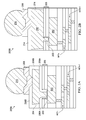
- FIG. 5 depicts a wafer on which a copper metallization layer that will receive wire bonding has been protected from corrosion according to the prior art
- FIG. 6 depicts a wafer on which a copper metallization layer that will be sent to a bump shop for the formation of a bump array has been protected from corrosion according to the prior art.
- a packaged chip can take place in multiple locations. For example, a wafer containing a few to several thousand chips can be fabricated at a first location. In some instances, fabrication can include writing specific information to a non-volatile memory on the chip, which then requires a probe of each chip to determine whether the information was correctly stored, thermal stressing of the wafer and a second probe of the chips to determine which chips failed under stress. The wafer may then be shipped to a second location where the chips can be separated and coupled to a lead frame or have a bump array or other forms of connectors formed.
- the metallization layers in the fabrication facility can be either copper or aluminum.
- the copper metallization layers in the fabrication facility are generally formed using a Damascene process that etches trenches in a dielectric layer and fills the trench with copper.
- metallization layers formed after a protective overcoat is provided on the chip are generally formed either by depositing a layer of aluminum, then patterning and etching the aluminum, or else by patterning a photoresist layer on the top layer of the chip and plating copper on the surface exposed by the photoresist.
- the deposition of bump metal generally consists of depositing a barrier layer followed by copper plating.
- the present application refers to fab metallization as opposed to bump shop metallization to distinguish between these two different metallization processes and the points in time at which they occur.
- This reference to bump shop metallization is not intended to be limiting to under-bump metallization, but serves as an example only.
- FIG. 5 depicts a prior art wafer 500 in which a final fab metallization layer is copper.
- Wafer 500 includes a substrate 502 in which various devices (not specifically shown) such as transistors, resistors, capacitors, etc. are formed.
- An inter-level dielectric (ILD) 504 has been formed over the substrate and metallization layers have been formed to connect devices on the chip to each other.
- ILD inter-level dielectric
- the metallization layers shown include metal N ⁇ 1 506 A, metal N 506 B and copper metallization layer 508 . Although three metallization layers are shown in this figure, the number of metallization layers can be fewer or greater than three as required by the design of the chip. The disclosed methodology is specific to copper in the final metallization layer 508 , but the other metallization layers can be either aluminum or copper. Vias 505 provide connections between the different interconnect layers.
- a protective overcoat 510 that is moisture impervious has been formed over the copper metallization layer 508 and ILD 504 for protection.
- protective overcoat 510 has two layers: an oxide layer 510 A, which can be silicon oxide, forms the layer directly over copper metallization layer 508 and a layer 510 B formed over the oxide layer 510 A can be either a nitride or an oxynitride.
- a window 512 has been opened in protective overcoat 510 to contact copper metallization layer 508 .
- a three-layer liner is formed in window 512 .
- a layer of tantalum nitride (TaN) 514 is provided as a barrier layer, followed by a layer of nickel (Ni) 516 . While these two layers provide a necessary barrier, they do not present a surface that is corrosion resistant and able to be probed.
- the final layer provided is palladium (Pd) 518 , which can be used for probing and will not corrode at the temperatures to which the chip will be subjected.
- the palladium layer 518 is typically about 1500 ⁇ thick. While the embodiment shown in FIG. 5 works well for chips that will receive wire bonding, this configuration will not work for other types of interconnects, such as bump arrays or other interconnection techniques.
- the problem with using this embodiment with further metallization is that the further metallization will not adhere to the palladium but will peel away.
- FIG. 6 depicts a schematic diagram of a wafer 600 having a copper connection that is protected against corrosion and which can be utilized to form a bump array.
- all elements below copper metallization layer 508 are the same as in FIG. 5 , but the solution utilized for corrosion resistance and the ability to be probed are different.
- a protective overcoat which in this embodiment is a first protective overcoat 602 is formed over the top of the copper metallization layer 508 and ILD 504 and a window (not specifically indicated) has been formed through the protective overcoat 602 to expose copper metallization layer 508 .
- a thin layer of tantalum nitride 604 is deposited over the surface of the protective overcoat 602 and the exposed copper metallization layer 508 .
- the tantalum nitride 604 is followed by a layer of aluminum 606 that forms a cap over the copper metallization layer 508 .
- This aluminum 606 is covered with a photoresist, which is patterned, and unnecessary portions of the aluminum 606 and TaN 604 are removed to form aluminum cap 607 .
- aluminum cap 607 is covered by a second protective overcoat 608 , which again includes oxide layer 608 A and oxynitride 608 B.
- the second protective overcoat 608 is then patterned and etched to open a second window 610 to expose the aluminum cap 607 .
- the aluminum cap 607 serves well to protect copper metallization layer 508 from corrosion and to allow probing where necessary.
- the wafer containing the aluminum cap 607 is received at a bump shop, the wafer can be cleaned, generally with a short sputter etching process, and the bump array can be formed according to known techniques. The entire process is well known and understood. However, because of the need for two masks to implement the aluminum cap, this process is expensive to utilize.
- the protection process that is in use for wire bonding applications while not being applicable for applications such as forming bump arrays, can be adapted for use with bump arrays and other connectors by thinning the final, corrosion-resistant layer to a point where the wafer cleaning process utilized at the bump shop can remove this layer, either completely or substantially. That is, rather than becoming a permanent part of the circuit being fabricated, the outer layer of the protective metal layers becomes a sacrificial layer.
- a sacrificial layer or, as also referred to, a sacrificial conductive stack is intended to cover both a conductive layer or layers that are completely sacrificial, i.e., is entirely removed during processing, and also to cover a conductive layer or layers that are substantially removed but may leave remnants or tags of material in difficult to remove locations.
- This latter situation can arise, for example, when a sputter etching process is utilized to remove the conductive stack from a recess, such as the opening to a metallization layer.
- the etch can successfully remove portions of the sacrificial conductive stack that are on the bottom of the opening, but leave portions of the conductive stack that are adjacent the sidewalls and/or corners of the opening. These remnants, when present, do not interfere with the creation of bumps or other connectors.
- the etching process can generally remove the sacrificial conductive stack entirely.
- FIG. 1 depicts an example of a wafer 100 containing IC chips on which a copper metallization layer is protected by a conductive stack to prevent corrosion, the conductive stack being partially sacrificial.
- a conductive stack to prevent corrosion
- the conductive stack being partially sacrificial.
- FIG. 1 depicts an example of a wafer 100 containing IC chips on which a copper metallization layer is protected by a conductive stack to prevent corrosion, the conductive stack being partially sacrificial.
- FIG. 1 depicts an example of a wafer 100 containing IC chips on which a copper metallization layer is protected by a conductive stack to prevent corrosion, the conductive stack being partially sacrificial.
- FIG. 1 depicts an example of a wafer 100 containing IC chips on which a copper metallization layer is protected by a conductive stack to prevent corrosion, the conductive stack being partially sacrificial.
- FIG. 1 depicts an example of a wafer 100 containing IC chips
- a window 108 is opened through the protective overcoat 106 to contact copper metallization layer 102 , two conductive stacks are deposited on the surface of wafer 100 to provide the necessary corrosion protection.
- the stacks serve two somewhat different purposes and each contains one or more layers of conductive material.
- the first stack is a barrier conductive stack 112 , which acts to provide a barrier between the copper metallization layer 102 and further layers.
- barrier conductive stack 112 comprises a layer of Ta or TaN 114 deposited to a thickness in the range of 100 ⁇ -800 ⁇ and the Ni 116 is deposited to a thickness in the range of 2000 ⁇ -30,000 ⁇ .
- Another embodiment of the barrier conductive stack 112 can include a layer of TaN followed by a layer of Ni and a further layer of TaN.
- a layer of TaN can be followed with a layer of tungsten (W), with or without a further layer of tantalum nitride.
- the second stack is a sacrificial conductive stack 118 that prevents oxidation of the barrier conductive stack and can also be utilized for probing of the wafer where necessary.
- Sacrificial conductive stack 118 can be a single layer, as shown in FIG. 1 .
- Suitable materials for sacrificial conductive stack 118 include, e.g., noble metals such as gold, platinum, palladium, and ruthenium, as well as any combination of these metals.
- Other conductive materials that are suitable for sacrificial conductive stack 118 include metals that do not significantly oxidize at or below 260° C., e.g., chromium.
- sacrificial conductive stack 118 has a thickness in the range of 50-500 ⁇ . In one embodiment, sacrificial conductive stack 118 has a thickness in the range of 50-400 ⁇ . In another embodiment, sacrificial conductive stack 118 has a thickness in the range of 50-250 ⁇ . In yet another embodiment, sacrificial conductive stack 118 has a thickness in the range of 50-100 ⁇ . Although shown as a single layer, sacrificial conductive stack 118 can include multiple sacrificial layers, e.g., platinum overlain with gold.
- FIGS. 2A-2G each depicts an IC chip 200 having a connection method that can utilize the disclosed sacrificial conductive stack to provide these connectors in a cost effective manner.
- Each of these examples utilizes the same basic wafer shown in FIGS. 1, 5 and 6 , but in each example, slightly different connectors are utilized or are tied to the copper metallization layer 202 in different ways.
- FIGS. 2A-2D each depicts an IC chip 200 A- 200 D having a form of under-bump-metallization formed according to embodiments of the disclosure.
- copper metallization layer 202 is coupled to a redistribution layer RDL 204 through the barrier conductive stack 203 .
- a first polyimide layer 206 A has been deposited over protective overcoat 205 prior to the formation of redistribution layer RDL 204 and a second polyimide layer 206 B has been deposited on top of redistribution layer 204 .
- Under-bump metal 208 has been formed in contact with the redistribution layer 204 and provides a landing area for solder bump 210 .
- a copper interconnect layer 212 has been formed on top of protective overcoat 205 and contacts copper metallization layer 202 through barrier conductive stack 203 , while polyimide 214 has been deposited on top of copper interconnect layer 212 .
- Under-bump metal 208 has been formed on top of polyimide 214 and in contact with copper interconnect layer 212 , with solder bump 210 formed on the under-bump metal 208 .
- FIG. 2C depicts an embodiment in which under-bump metal 208 is separated from the protective overcoat 205 only by polyimide 216 and directly contacts barrier conductive stack 203 to couple to copper metallization layer 202 .
- FIG. 2D depicts a further embodiment in which under-bump metal 208 has been formed on top of protective overcoat 205 and directly contacts barrier conductive stack 203 to couple to copper metallization 202 .
- Other variations on these embodiments are also possible.
- FIGS. 2E-2G depict other IC chips 200 E- 200 G having means of providing couplings with a further chip.
- a copper pillar 218 is coupled to copper metallization layer 202 through barrier conductive stack 203 and is also separated from protective overcoat 205 by polyimide 220 .
- the polyimide layer is omitted and a metal bonding layer METTOP 222 has been deposited directly overlying protective overcoat 205 and barrier conductive stack 203 to provide a coupling to copper metallization layer 202 .
- FIG. 2E depict other IC chips 200 E- 200 G having means of providing couplings with a further chip.
- a copper pillar 218 is coupled to copper metallization layer 202 through barrier conductive stack 203 and is also separated from protective overcoat 205 by polyimide 220 .
- the polyimide layer is omitted and a metal bonding layer METTOP 222 has been deposited directly overlying protective overcoat 205 and barrier conductive stack 203 to provide a coup
- FIG. 2G depicts an embodiment in which metal bonding layer METTOP 224 is deposited overlying protective overcoat 205 and barrier conductive stack 203 , then etched, followed by deposition of polyimide 228 .
- a copper post 226 provides a contact to metal bonding layer METTOP 203 .
- FIG. 3 depicts a flowchart for a method 300 of utilizing a sacrificial conductive stack to prevent corrosion of a copper metallization layer according to an embodiment of the disclosure.
- active devices have already been formed on an IC chip, as well as metallization layers that couple devices on the chip with each other.
- a top metallization layer which is of copper, has been covered with a passivation overcoat.
- a typical passivation may consist of oxynitride, silicon nitride, a combination of silicon dioxide and oxynitride, or a combination of silicon dioxide and silicon nitride.
- Method 300 starts with opening 305 a window on a first surface of the IC chip through the passivation overcoat to expose the copper metallization layer.
- the window as having sidewalls, which are adjacent the passivation overcoat, and a bottom that is adjacent the copper metallization layer.
- Method 300 continues with depositing 310 a barrier conductive stack on the passivation overcoat and the exposed portions of the copper metallization layer.
- the barrier conductive stack includes a layer of TaN with a layer of Ni on top of the TaN.
- a sacrificial conductive stack is then deposited 315 on the barrier conductive stack.
- the sacrificial conductive stack has a thickness between 50 ⁇ and 500 ⁇ .
- the sacrificial conductive stack is formed of palladium.
- the first surface of the semiconductor chip is polished 320 to remove the sacrificial conductive stack and the barrier conductive stack from the surface of the passivation overcoat.
- the copper metallization layer is the last metallization layer that is formed at the fabrication facility, with other metallization processes such as preparing the chip for coupling to a printed circuit board or to other chips being performed at other facilities.
- data is written 325 to memory that has been formed on the chip. This can be performed utilizing probes and the access to the copper metallization layer provided by the sacrificial conductive stack and the barrier conductive stack. Once the data is written, heat stressing can be performed 330 on the chip by a bake cycle. This is followed by reading 335 the data from the memory to test for retention. Memories that do not retain the data can be marked and will not be shipped to a customer. Each of elements 325 , 330 , 335 is shown within dotted lines to indicate that they are optional.
- memory testing is followed with removal of the sacrificial conductive stack from the window that was previously created.
- method 300 continues with performing an etching process 340 to remove the sacrificial conductive stack from at least the bottom of the window. If the etching process is a wet etch, the sacrificial conductive stack is also removed from the sides of the window, although this is not necessary to the process. In addition to removing the sacrificial conductive stack, the etching process also removes any contaminants that may have been introduced during reading of the memory.
- a further metallization layer is formed 345 that substantially fills the window.
- the further metallization layer completely fills the window.
- a dielectric layer such as a polyimide layer is first deposited on the protective overcoat and a smaller window opened through the dielectric layer to contact the copper metallization layer.
- the further metallization layer fills the smaller window and substantially fills the original window.
- the further metallization layer can be any of the processes shown in FIGS. 2A-2G or any other metallization process, whether currently known or unknown.
- FIG. 4 depicts a flowchart for a method 400 of forming interconnections over a copper metallization layer. This method would generally be performed at a bump facility or similar facility.
- Method 400 begins with receiving 405 a semiconductor chip that comprises a window through a protective overcoat to a copper metallization layer. When received, the window has a barrier conductive stack adjacent the copper metallization layer and the protective overcoat and a sacrificial conductive stack adjacent the barrier conductive stack.
- the facility performs 410 an etching process to remove the sacrificial conductive stack.
- the process does not require any additional time to remove the sacrificial conductive stack than would normally be allotted for the removal of contaminants. In one embodiment, additional time for removal of the sacrificial conductive stack is minimal.
- the etching process may remove only the portion of the sacrificial conductive stack that lies on the bottom of the window or the etching process may remove all portions of the sacrificial conductive stack. In either case, the etching process can be followed by forming 415 a further metallization layer that couples to the copper metallization layer through the barrier conductive stack. This process of forming the further metallization layer can utilize any method, whether currently known or unknown.
Landscapes
- Engineering & Computer Science (AREA)
- Computer Hardware Design (AREA)
- Microelectronics & Electronic Packaging (AREA)
- Power Engineering (AREA)
- Manufacturing & Machinery (AREA)
- Physics & Mathematics (AREA)
- Condensed Matter Physics & Semiconductors (AREA)
- General Physics & Mathematics (AREA)
- Chemical & Material Sciences (AREA)
- Chemical Kinetics & Catalysis (AREA)
- General Chemical & Material Sciences (AREA)
- Internal Circuitry In Semiconductor Integrated Circuit Devices (AREA)
Abstract
Description
Claims (20)
Priority Applications (7)
| Application Number | Priority Date | Filing Date | Title |
|---|---|---|---|
| US15/858,145 US10490448B2 (en) | 2017-12-29 | 2017-12-29 | Method of using a sacrificial conductive stack to prevent corrosion |
| JP2020536657A JP7339486B2 (en) | 2017-12-29 | 2018-12-31 | Method using a sacrificial conductive stack to prevent corrosion |
| CN201880076029.4A CN111418059A (en) | 2017-12-29 | 2018-12-31 | Method for preventing corrosion using sacrificial conductive stack |
| EP18895397.0A EP3732709A4 (en) | 2017-12-29 | 2018-12-31 | Method of using a sacrificial conductive stack to prevent corrosion |
| PCT/US2018/068109 WO2019133954A1 (en) | 2017-12-29 | 2018-12-31 | Method of using a sacrificial conductive stack to prevent corrosion |
| US16/661,782 US10811312B2 (en) | 2017-12-29 | 2019-10-23 | Method of using a sacrificial conductive stack to prevent corrosion |
| JP2023124080A JP2023153915A (en) | 2017-12-29 | 2023-07-31 | Method of using sacrificial conductive stack for preventing corrosion |
Applications Claiming Priority (1)
| Application Number | Priority Date | Filing Date | Title |
|---|---|---|---|
| US15/858,145 US10490448B2 (en) | 2017-12-29 | 2017-12-29 | Method of using a sacrificial conductive stack to prevent corrosion |
Related Child Applications (1)
| Application Number | Title | Priority Date | Filing Date |
|---|---|---|---|
| US16/661,782 Continuation US10811312B2 (en) | 2017-12-29 | 2019-10-23 | Method of using a sacrificial conductive stack to prevent corrosion |
Publications (2)
| Publication Number | Publication Date |
|---|---|
| US20190206730A1 US20190206730A1 (en) | 2019-07-04 |
| US10490448B2 true US10490448B2 (en) | 2019-11-26 |
Family
ID=67058495
Family Applications (2)
| Application Number | Title | Priority Date | Filing Date |
|---|---|---|---|
| US15/858,145 Active US10490448B2 (en) | 2017-12-29 | 2017-12-29 | Method of using a sacrificial conductive stack to prevent corrosion |
| US16/661,782 Active US10811312B2 (en) | 2017-12-29 | 2019-10-23 | Method of using a sacrificial conductive stack to prevent corrosion |
Family Applications After (1)
| Application Number | Title | Priority Date | Filing Date |
|---|---|---|---|
| US16/661,782 Active US10811312B2 (en) | 2017-12-29 | 2019-10-23 | Method of using a sacrificial conductive stack to prevent corrosion |
Country Status (5)
| Country | Link |
|---|---|
| US (2) | US10490448B2 (en) |
| EP (1) | EP3732709A4 (en) |
| JP (2) | JP7339486B2 (en) |
| CN (1) | CN111418059A (en) |
| WO (1) | WO2019133954A1 (en) |
Families Citing this family (1)
| Publication number | Priority date | Publication date | Assignee | Title |
|---|---|---|---|---|
| US11715756B2 (en) * | 2021-04-09 | 2023-08-01 | Taiwan Semiconductor Manufacturing Company, Ltd. | Device structure and methods of forming the same |
Citations (11)
| Publication number | Priority date | Publication date | Assignee | Title |
|---|---|---|---|---|
| US20030155408A1 (en) * | 2002-02-19 | 2003-08-21 | International Business Machines Corporation | Sacrificial seed layer process for forming c4 solder bumps |
| US20050224987A1 (en) * | 2004-04-07 | 2005-10-13 | Hortaleza Edgardo R | Structure and method for contact pads having double overcoat-protected bondable metal plugs over copper-metallized integrated circuits |
| US20060016861A1 (en) * | 2004-07-21 | 2006-01-26 | International Business Machines Corporation | Damascene patterning of barrier layer metal for C4 solder bumps |
| US7026225B1 (en) * | 2003-09-09 | 2006-04-11 | Advanced Micro Devices, Inc. | Semiconductor component and method for precluding stress-induced void formation in the semiconductor component |
| US20080050905A1 (en) | 2006-05-29 | 2008-02-28 | Kabushiki Kaisha Toshiba | Method of manufacturing semiconductor device |
| US7585759B2 (en) * | 2005-07-29 | 2009-09-08 | Advanced Micro Devices, Inc. | Technique for efficiently patterning an underbump metallization layer using a dry etch process |
| US20100155949A1 (en) * | 2008-12-24 | 2010-06-24 | Texas Instruments Incorporated | Low cost process flow for fabrication of metal capping layer over copper interconnects |
| US7759768B2 (en) * | 2002-04-29 | 2010-07-20 | Infineon Technologies Ag | Integrated circuit with intergrated capacitor and methods for making same |
| US20140264861A1 (en) | 2013-03-15 | 2014-09-18 | Applied Materials, Incorporated | Sputter etch processing for heavy metal patterning in integrated circuits |
| US20150179592A1 (en) | 2013-12-19 | 2015-06-25 | Texas Instruments Incorporated | Self-aligned under bump metal |
| US9508666B2 (en) * | 2011-05-30 | 2016-11-29 | Taiwan Semiconductor Manufacturing Company, Ltd. | Packaging structures and methods with a metal pillar |
Family Cites Families (8)
| Publication number | Priority date | Publication date | Assignee | Title |
|---|---|---|---|---|
| JP2001094043A (en) * | 1999-09-20 | 2001-04-06 | Rohm Co Ltd | Semiconductor chip |
| US7709958B2 (en) * | 2004-06-18 | 2010-05-04 | Uri Cohen | Methods and structures for interconnect passivation |
| US20070117377A1 (en) * | 2005-11-23 | 2007-05-24 | Chih-Chao Yang | Conductor-dielectric structure and method for fabricating |
| US20070298620A1 (en) * | 2006-06-27 | 2007-12-27 | Kuang-Yeh Chang | Surface treatment, sorting and assembling methods of microelectronic devices and storage structure thereof |
| US20080113508A1 (en) * | 2006-11-13 | 2008-05-15 | Akolkar Rohan N | Method of fabricating metal interconnects using a sacrificial layer to protect seed layer prior to gap fill |
| US20080237860A1 (en) * | 2007-03-27 | 2008-10-02 | Tokyo Electron Limited | Interconnect structures containing a ruthenium barrier film and method of forming |
| JP2009194195A (en) * | 2008-02-15 | 2009-08-27 | Panasonic Corp | Semiconductor device and method of manufacturing the same |
| US9412654B1 (en) * | 2015-04-27 | 2016-08-09 | International Business Machines Corporation | Graphene sacrificial deposition layer on beol copper liner-seed for mitigating queue-time issues between liner and plating step |
-
2017
- 2017-12-29 US US15/858,145 patent/US10490448B2/en active Active
-
2018
- 2018-12-31 EP EP18895397.0A patent/EP3732709A4/en active Pending
- 2018-12-31 WO PCT/US2018/068109 patent/WO2019133954A1/en unknown
- 2018-12-31 JP JP2020536657A patent/JP7339486B2/en active Active
- 2018-12-31 CN CN201880076029.4A patent/CN111418059A/en active Pending
-
2019
- 2019-10-23 US US16/661,782 patent/US10811312B2/en active Active
-
2023
- 2023-07-31 JP JP2023124080A patent/JP2023153915A/en active Pending
Patent Citations (11)
| Publication number | Priority date | Publication date | Assignee | Title |
|---|---|---|---|---|
| US20030155408A1 (en) * | 2002-02-19 | 2003-08-21 | International Business Machines Corporation | Sacrificial seed layer process for forming c4 solder bumps |
| US7759768B2 (en) * | 2002-04-29 | 2010-07-20 | Infineon Technologies Ag | Integrated circuit with intergrated capacitor and methods for making same |
| US7026225B1 (en) * | 2003-09-09 | 2006-04-11 | Advanced Micro Devices, Inc. | Semiconductor component and method for precluding stress-induced void formation in the semiconductor component |
| US20050224987A1 (en) * | 2004-04-07 | 2005-10-13 | Hortaleza Edgardo R | Structure and method for contact pads having double overcoat-protected bondable metal plugs over copper-metallized integrated circuits |
| US20060016861A1 (en) * | 2004-07-21 | 2006-01-26 | International Business Machines Corporation | Damascene patterning of barrier layer metal for C4 solder bumps |
| US7585759B2 (en) * | 2005-07-29 | 2009-09-08 | Advanced Micro Devices, Inc. | Technique for efficiently patterning an underbump metallization layer using a dry etch process |
| US20080050905A1 (en) | 2006-05-29 | 2008-02-28 | Kabushiki Kaisha Toshiba | Method of manufacturing semiconductor device |
| US20100155949A1 (en) * | 2008-12-24 | 2010-06-24 | Texas Instruments Incorporated | Low cost process flow for fabrication of metal capping layer over copper interconnects |
| US9508666B2 (en) * | 2011-05-30 | 2016-11-29 | Taiwan Semiconductor Manufacturing Company, Ltd. | Packaging structures and methods with a metal pillar |
| US20140264861A1 (en) | 2013-03-15 | 2014-09-18 | Applied Materials, Incorporated | Sputter etch processing for heavy metal patterning in integrated circuits |
| US20150179592A1 (en) | 2013-12-19 | 2015-06-25 | Texas Instruments Incorporated | Self-aligned under bump metal |
Non-Patent Citations (1)
| Title |
|---|
| Patent Cooperation Treaty Search Report, dated Apr. 18, 2019, International Application No. PCT/US2018/068109. |
Also Published As
| Publication number | Publication date |
|---|---|
| US20190206730A1 (en) | 2019-07-04 |
| US20200058547A1 (en) | 2020-02-20 |
| JP7339486B2 (en) | 2023-09-06 |
| EP3732709A4 (en) | 2021-02-24 |
| CN111418059A (en) | 2020-07-14 |
| US10811312B2 (en) | 2020-10-20 |
| EP3732709A1 (en) | 2020-11-04 |
| WO2019133954A1 (en) | 2019-07-04 |
| JP2023153915A (en) | 2023-10-18 |
| JP2021509541A (en) | 2021-03-25 |
Similar Documents
| Publication | Publication Date | Title |
|---|---|---|
| US7307342B2 (en) | Interconnection structure of integrated circuit chip | |
| US6451681B1 (en) | Method of forming copper interconnection utilizing aluminum capping film | |
| US8937009B2 (en) | Far back end of the line metallization method and structures | |
| US6861344B2 (en) | Method of manufacturing a semiconductor integrated circuit device | |
| US10777523B2 (en) | Semiconductor devices and semiconductor devices including a redistribution layer | |
| EP0813238B1 (en) | Flip-Chip Semiconductor device with test structure and method of manufacturing the same | |
| US20030020163A1 (en) | Bonding pad structure for copper/low-k dielectric material BEOL process | |
| KR102411064B1 (en) | Methods for fabricating semiconductor devices having through electrodes and methods for fabricating the same | |
| US9691703B2 (en) | Bond pad structure with dual passivation layers | |
| JPH0829451A (en) | Bump semiconductor device and probe inspection method thereof | |
| JP2001015403A (en) | Semiconductor device | |
| US20090166861A1 (en) | Wire bonding of aluminum-free metallization layers by surface conditioning | |
| JP2006203215A (en) | Semiconductor integrated circuit device and method of manufacturing the same | |
| US8283247B2 (en) | Semiconductor device including a die region designed for aluminum-free solder bump connection and a test structure designed for aluminum-free wire bonding | |
| TW201839940A (en) | A semiconductor package having exposed redistribution layer features and related methods of packaging and testing | |
| US8691600B2 (en) | Method for testing through-silicon-via (TSV) structures | |
| JP2023153915A (en) | Method of using sacrificial conductive stack for preventing corrosion | |
| US7573142B2 (en) | Alignment key structure in a semiconductor device and method of forming the same | |
| JP2010034595A (en) | Semiconductor integrated circuit device and its manufacturing method |
Legal Events
| Date | Code | Title | Description |
|---|---|---|---|
| AS | Assignment |
Owner name: TEXAS INSTRUMENTS INCORPORATED, TEXAS Free format text: ASSIGNMENT OF ASSIGNORS INTEREST;ASSIGNOR:JAIN, MANOJ K.;REEL/FRAME:044505/0953 Effective date: 20171228 |
|
| FEPP | Fee payment procedure |
Free format text: ENTITY STATUS SET TO UNDISCOUNTED (ORIGINAL EVENT CODE: BIG.); ENTITY STATUS OF PATENT OWNER: LARGE ENTITY |
|
| STPP | Information on status: patent application and granting procedure in general |
Free format text: NOTICE OF ALLOWANCE MAILED -- APPLICATION RECEIVED IN OFFICE OF PUBLICATIONS |
|
| STPP | Information on status: patent application and granting procedure in general |
Free format text: PUBLICATIONS -- ISSUE FEE PAYMENT VERIFIED |
|
| STCF | Information on status: patent grant |
Free format text: PATENTED CASE |
|
| MAFP | Maintenance fee payment |
Free format text: PAYMENT OF MAINTENANCE FEE, 4TH YEAR, LARGE ENTITY (ORIGINAL EVENT CODE: M1551); ENTITY STATUS OF PATENT OWNER: LARGE ENTITY Year of fee payment: 4 |