US10475802B2 - Semiconductor device - Google Patents
Semiconductor device Download PDFInfo
- Publication number
- US10475802B2 US10475802B2 US15/812,525 US201715812525A US10475802B2 US 10475802 B2 US10475802 B2 US 10475802B2 US 201715812525 A US201715812525 A US 201715812525A US 10475802 B2 US10475802 B2 US 10475802B2
- Authority
- US
- United States
- Prior art keywords
- semiconductor layer
- nitride semiconductor
- electrode
- gate
- extraction electrode
- Prior art date
- Legal status (The legal status is an assumption and is not a legal conclusion. Google has not performed a legal analysis and makes no representation as to the accuracy of the status listed.)
- Active
Links
Images


Classifications
-
- H—ELECTRICITY
- H10—SEMICONDUCTOR DEVICES; ELECTRIC SOLID-STATE DEVICES NOT OTHERWISE PROVIDED FOR
- H10B—ELECTRONIC MEMORY DEVICES
- H10B41/00—Electrically erasable-and-programmable ROM [EEPROM] devices comprising floating gates
-
- H01L27/11517—
-
- H01L29/0649—
-
- H01L29/42316—
-
- H01L29/7786—
-
- H—ELECTRICITY
- H10—SEMICONDUCTOR DEVICES; ELECTRIC SOLID-STATE DEVICES NOT OTHERWISE PROVIDED FOR
- H10D—INORGANIC ELECTRIC SEMICONDUCTOR DEVICES
- H10D30/00—Field-effect transistors [FET]
- H10D30/40—FETs having zero-dimensional [0D], one-dimensional [1D] or two-dimensional [2D] charge carrier gas channels
- H10D30/47—FETs having zero-dimensional [0D], one-dimensional [1D] or two-dimensional [2D] charge carrier gas channels having two-dimensional [2D] charge carrier gas channels, e.g. nanoribbon FETs or high electron mobility transistors [HEMT]
- H10D30/471—High electron mobility transistors [HEMT] or high hole mobility transistors [HHMT]
- H10D30/475—High electron mobility transistors [HEMT] or high hole mobility transistors [HHMT] having wider bandgap layer formed on top of lower bandgap active layer, e.g. undoped barrier HEMTs such as i-AlGaN/GaN HEMTs
-
- H—ELECTRICITY
- H10—SEMICONDUCTOR DEVICES; ELECTRIC SOLID-STATE DEVICES NOT OTHERWISE PROVIDED FOR
- H10D—INORGANIC ELECTRIC SEMICONDUCTOR DEVICES
- H10D62/00—Semiconductor bodies, or regions thereof, of devices having potential barriers
- H10D62/10—Shapes, relative sizes or dispositions of the regions of the semiconductor bodies; Shapes of the semiconductor bodies
- H10D62/113—Isolations within a component, i.e. internal isolations
- H10D62/115—Dielectric isolations, e.g. air gaps
-
- H—ELECTRICITY
- H10—SEMICONDUCTOR DEVICES; ELECTRIC SOLID-STATE DEVICES NOT OTHERWISE PROVIDED FOR
- H10D—INORGANIC ELECTRIC SEMICONDUCTOR DEVICES
- H10D64/00—Electrodes of devices having potential barriers
- H10D64/20—Electrodes characterised by their shapes, relative sizes or dispositions
- H10D64/27—Electrodes not carrying the current to be rectified, amplified, oscillated or switched, e.g. gates
- H10D64/311—Gate electrodes for field-effect devices
- H10D64/411—Gate electrodes for field-effect devices for FETs
-
- H01L29/2003—
-
- H01L29/41725—
-
- H—ELECTRICITY
- H10—SEMICONDUCTOR DEVICES; ELECTRIC SOLID-STATE DEVICES NOT OTHERWISE PROVIDED FOR
- H10D—INORGANIC ELECTRIC SEMICONDUCTOR DEVICES
- H10D62/00—Semiconductor bodies, or regions thereof, of devices having potential barriers
- H10D62/80—Semiconductor bodies, or regions thereof, of devices having potential barriers characterised by the materials
- H10D62/85—Semiconductor bodies, or regions thereof, of devices having potential barriers characterised by the materials being Group III-V materials, e.g. GaAs
- H10D62/8503—Nitride Group III-V materials, e.g. AlN or GaN
-
- H—ELECTRICITY
- H10—SEMICONDUCTOR DEVICES; ELECTRIC SOLID-STATE DEVICES NOT OTHERWISE PROVIDED FOR
- H10D—INORGANIC ELECTRIC SEMICONDUCTOR DEVICES
- H10D64/00—Electrodes of devices having potential barriers
- H10D64/20—Electrodes characterised by their shapes, relative sizes or dispositions
- H10D64/23—Electrodes carrying the current to be rectified, amplified, oscillated or switched, e.g. sources, drains, anodes or cathodes
- H10D64/251—Source or drain electrodes for field-effect devices
Definitions
- the present disclosure relates to a semiconductor device, and particularly to a field effect transistor.
- Group III-V nitride based compound semiconductors typified by gallium nitride (GaN), so-called a nitride semiconductor, has been attracting attention.
- a nitride semiconductor is a compound semiconductor expressed by the following general expression: In x Ga y Al 1 ⁇ x ⁇ y N (0 ⁇ x ⁇ 1, 0 ⁇ y ⁇ 1, x+y ⁇ 1), and includes: aluminum (Al), gallium (Ga), and indium (In) included in group-III elements; and nitrogen (N) included in group-V elements.
- the nitride semiconductor makes it possible to form various mixed crystals, and easily form a heterojunction interface.
- a heterojunction of a nitride semiconductor has the following characteristics: a high-concentration two-dimensional electron gas layer (2DEG layer) is generated at a junction interface by spontaneous polarization or piezoelectric polarization even in a state without doping. Therefore, it becomes possible to manufacture a high-breakdown and miniaturized device making use of characteristics of the material having not only a wide band gap of 3.4 (eV) but also a high breakdown field of 3.3 (MV/cm).
- a field effect transistor (FET) using this high-concentration 2DEG layer as a carrier has been attracting attention as a device for high frequency, high speed, and large current.
- a field effect transistor using a nitride semiconductor can be device-designed to be smaller in size as compared with a field effect transistor using silicon (Si).
- Si silicon
- Japanese Unexamined Patent Application Publication No. 2012-119625 discloses a semiconductor device which includes means for suppressing self turn-on.
- FIG. 19 is a schematic plan view of the semiconductor device described in Japanese Unexamined Patent Application Publication No, 2012-119625.
- the semiconductor device described in Japanese Unexamined Patent Application Publication No, 2012-119625 has a structure in which a distance between gate pad 810 and source pad 811 which are disposed via non-element isolation region 820 is smaller than a distance between gate pad 810 and drain pad 812 which are disposed via non-element isolation region 819 .
- the self turn-on is suppressed by adding the gate-source capacitance Cgs between gate pad 810 and source pad 811 and thus reducing the gate-drain capacitance Cgd/gate-source capacitance Cgs ratio.
- the semiconductor device disclosed in Japanese Unexamined Patent Application Publication No. 2012-119625 can increase the gate-source capacitance Cgs, however, there is the following problem.
- Japanese Unexamined Patent Application Publication No. 2012-119625 discloses, for example, a method of forming an active region including a 2DEG layer between gate pad 810 and source pad 811 .
- the method that only increases the gate-source capacitance Cgs self turn-on can be suppressed but the gate-source charge quantity (Qgs) increases. Therefore, the gate drive loss and switching delay time also increase. Accordingly, there is a limit to the measure for suppressing self turn-on by only increasing the gate-source capacitance Cgs.
- the present disclosure has been conceived to solve the above-described problem, and has an object to provide a semiconductor device which can operate a field effect transistor at high speed without malfunction and has high electrostatic resistance.
- a semiconductor device includes: a substrate; a semiconductor layer stacked body including a first nitride semiconductor layer above the substrate and a second nitride semiconductor layer which is on the first nitride semiconductor layer and has a band gap wider than a band gap of the first nitride semiconductor layer; a gate electrode on the semiconductor layer stacked body; a source electrode and a drain electrode located on opposite sides of the gate electrode and spaced apart from the gate electrode in a plan view of the semiconductor layer stacked body; a first active region which includes the source electrode, the drain electrode and the gate electrode in the plan view, and has a first carrier layer located in the first nitride semiconductor layer; a second active region which is on an extension of a long-side direction of the drain electrode in the plan view, and has a second carrier layer located in the first nitride semiconductor layer via an element isolation region containing no carrier; a gate extraction electrode located opposite a short side of the
- the semiconductor device according to the present disclosure it is possible to realize a semiconductor device which can operate a field effect transistor at high speed without malfunction and has high electrostatic resistance.
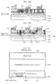
- FIG. 1A is a schematic plan view of a nitride semiconductor device according to Embodiment 1;
- FIG. 1B is a schematic cross-sectional view of the nitride semiconductor device according to Embodiment 1;
- FIG. 2 is a schematic plan view of a semiconductor device according to Variation 1 of Embodiment 1;
- FIG. 3 is a schematic plan view of the semiconductor device according to Variation 1 of Embodiment 1;
- FIG. 4 is a schematic cross-sectional view of a semiconductor device according to Variation 2 of Embodiment 1;
- FIG. 5 is a schematic cross-sectional view f a semiconductor device according to Variation 3 of Embodiment 1;
- FIG. 6 is a schematic cross-sectional view of a semiconductor device according to Variation 4 of Embodiment 1;
- FIG. 7 is a schematic cross-sectional view of a semiconductor device according to Variation 5 of Embodiment 1;
- FIG. 8 is a schematic cross-sectional view of a semiconductor device according to Variation 6 of Embodiment 1;
- FIG. 9 is a schematic cross-sectional view of a semiconductor device according to Variation 7 of Embodiment 1;
- FIG. 10 is a schematic cross-sectional view of a semiconductor device according to Variation 8 of Embodiment 1;
- FIG. 11 is a schematic cross-sectional view of a semiconductor device according to Variation 9 of Embodiment 1;
- FIG. 12 is a schematic cross-sectional view of a semiconductor device according to Variation 10 of Embodiment 1;
- FIG. 13 is a schematic cross-sectional view of a semiconductor device according to Variation 11 of Embodiment 1;
- FIG. 14 is a schematic plan view of a semiconductor device according to Embodiment 2.
- FIG. 15A is a first schematic cross-sectional view of the nitride semiconductor device according to Embodiment 2;
- FIG. 15B is a second schematic cross-sectional view of the nitride semiconductor device according to Embodiment 2;
- FIG. 16A is a capacitance reduction mechanism of the conventional semiconductor device
- FIG. 16B is a capacitance reduction mechanism of the nitride semiconductor device according to Embodiment 1;
- FIG. 17A is a first capacitance reduction mechanism of the conventional semiconductor device
- FIG. 17B is a first capacitance reduction mechanism of the nitride semiconductor device according to Embodiment 2;
- FIG. 18A is a first capacitance reduction mechanism of the conventional semiconductor device
- FIG. 18B is the first capacitance reduction mechanism of the nitride semiconductor device according to Embodiment 2.
- FIG. 19 is a schematic plan view of the semiconductor device described in Japanese Unexamined Patent Application Publication No. 2012-119625.
- FIG. 1A is a schematic plan view of nitride semiconductor device 1 according to Embodiment 1
- FIG. 1B is a schematic cross-sectional view of nitride semiconductor device 1 according to Embodiment 1.
- FIG. 1B illustrates a cross-sectional view, at an IB-IB line, of FIG. 1A .
- semiconductor device 1 includes substrate 101 , buffer layer 102 , first nitride semiconductor layer 103 , second nitride semiconductor layer 104 , source electrode 106 , drain electrode 107 and gate electrode 108 , gate extraction electrode 111 , and source extraction electrode 112 .
- Substrate 101 is, for example, a substrate including silicon.
- Buffer layer 102 is on substrate 101 and is a superlattice layer.
- First nitride semiconductor layer 103 is a GaN layer which is on buffer layer 102 and has a thickness of approximately 2 ⁇ m, for example.
- Second nitride semiconductor layer 104 is an AlGaN layer which is on first nitride semiconductor layer 103 and has a thickness of approximately 50 nm, for example.
- first nitride semiconductor layer 103 at an interface region with second nitride semiconductor layer 104 , two-dimensional electron gas (2DEG) is generated and there is a channel region having carrier layer 114 (collective term for first carrier layer 114 A and second carrier layer 114 B illustrated in FIG. 1B ).
- First nitride semiconductor layer 103 and second nitride semiconductor layer 104 constitute semiconductor layer stacked body 105 .
- semiconductor device 1 includes, in a plan view of semiconductor layer stacked body 105 , first active region 109 having a transistor function, and second active region 113 spaced apart from first active region 109 via element isolation region 110 .
- Source electrode 106 , drain electrode 107 , and gate electrode 108 are disposed in first active region 109 and on second nitride semiconductor layer 104 .
- First active region 109 includes source electrode 106 , drain electrode 107 , and gate electrode 108 in a plan view of semiconductor layer stacked body 105 , and has first carrier layer 114 A located in first nitride semiconductor layer 103 .
- Source electrode 106 and drain electrode 107 are each a laminated body including, for example, at least one of titanium (Ti) and Al.
- gate electrode 108 is between source electrode 106 and drain electrode 107 , and is a laminated body including, for example, at least one of Ti, Al, titanium nitride (TiN), palladium (Pd), platinum (Pt), gold (Au), and nickel (Ni). Note that although a short side of drain electrode 107 is inside first active region 109 in FIG. 1A and FIG. 2 and FIG. 3 described later, the short side of drain electrode 107 may coincide with an end of first active region 109 or may be beyond first active region 109 .
- Gate extraction electrode 111 is connected with gate electrode 108 across element isolation region 110 .
- Gate extraction electrode 111 is, in a plan view of semiconductor layer stacked body 105 , disposed in second active region 113 and located opposite the short side of drain electrode 107 , so as to extract a potential of gate electrode 108 .
- Source extraction electrode 112 is spaced apart from gate extraction electrode 111 and is electrically connected with source electrode 106 .
- source extraction electrode 112 is disposed in second active region 113 and adjacent to gate extraction electrode 111 .
- first nitride semiconductor layer 103 has second carrier layer 114 B.
- Second active region 113 is on an extension of a long-side direction of drain electrode 107 in the plan view, and has second carrier layer 114 B located in first nitride semiconductor layer 103 via element isolation region 110 containing no carrier.
- Element isolation region 110 is a region for spacing first active region 109 and second active region 113 apart from each other, and may be formed by ion implantation of, for example, at least one of boron (B) and argon (Ar), or may be a recess formed by etching.
- gate-drain capacitance Cgd is represented as the coupling capacitance between drain electrode 107 and gate extraction electrode 111 via the stacked structure from substrate 101 to second nitride semiconductor layer 104 .
- a potential of second carrier layer 114 that is in first nitride semiconductor layer 103 is substantially the same as a potential of source extraction electrode 112 , or an intermediate potential of a potential of gate extraction electrode 111 and the potential of source extraction electrode 112 . Therefore, gate-drain capacitance Cgd can be reduced.
- gate extraction electrode 111 is connected with second carrier layer 114 B via second nitride semiconductor layer 104 , the capacitance of second nitride semiconductor layer 104 is all given as gate-source capacitance Cgs.
- Disposing gate extraction electrode 111 , source extraction electrode 112 , and second carrier layer 114 B in second active region 113 as described above allows reducing Cgd as well as increasing Cgs due to parasitic Cgs given, which reduces Cgd/Cgs ratio. With this, self turn-on can be suppressed, and ESI) tolerance between gate electrode 108 and source electrode 106 can also be improved.
- second carrier layer 114 B is provided under gate extraction electrode 111 opposed to drain electrode 107 , and by setting the potential of second carrier layer 114 B to a source potential, a gate-source capacitance Cgs is added from gate extraction electrode 111 through second carrier layer 114 B, Conventionally, gate-drain capacitance Cgd was added by the drain electrode and the gate extraction electrode being opposed to each other.
- second carrier layer 114 B has the source potential, which produces an advantageous effect of shielding gate extraction electrode 111 and can reduce gate-drain capacitance Cgd. This makes it possible to reduce the Cgd/Cgs ratio and to suppress self turn-on. Furthermore, with Cgs added, electro-static discharge (ESD) tolerance between the gate electrode and the source electrode can also be improved.
- ESD electro-static discharge
- FIG. 16A is a capacitance reduction mechanism of the conventional semiconductor device. As illustrated in FIG. 16A , conventionally, gate-drain capacitance Cgd 115 was added via first carrier layer 114 A by drain electrode 107 and gate extraction electrode 111 being opposed to each other.
- FIG. 16B is a capacitance reduction mechanism of semiconductor device 1 according to Embodiment 1.
- second carrier layer 114 B has a source potential with respect to carrier layer resistance 117 A via contact resistance 116 A to carrier layer 114 , which causes capacitive coupling of gate-source capacitance Cgs 118 between gate extraction electrode 111 .
- gate-drain capacitance Cgd 115 is reduced and drain-source capacitance Cds 119 is increased. Since the increase in drain-source capacitance Cds 119 is a small amount with respect to the value of total Cds, there is no operational influence.
- a potential of second carrier layer 114 B in second active region 113 may be a source potential, and a potential from source extraction electrode 112 through second carrier layer 114 B in second active region 113 may be an intermediate potential between a potential of gate extraction electrode 111 and a potential of source extraction electrode 112 caused by capacitive coupling using an insulating film or coupling using Schottky junction.
- FIG. 2 and FIG. 3 are each a schematic plan view of a semiconductor device according to Variation 1 of Embodiment 1. Note that their cross-sectional views are omitted since they are similar to those in Embodiment 1.
- description on constituent elements which are the same as those in semiconductor device 1 according to Embodiment 1 will be omitted, and different constituent elements will be mainly described.
- terminal portion of gate electrode 208 is connected to gate extraction electrode 211 , and second active region 213 encloses the periphery of first active region 109 .
- gate extraction electrode 221 may also enclose first active region 109 .
- second active region 213 encloses the periphery of first active region 109 as in semiconductor device 2 A illustrated in FIG. 2 and semiconductor device 2 B illustrated in FIG. 3 .
- gate-drain capacitance Cgd in both terminal portions of gate electrode 208 .
- a gate-source capacitance Cgs larger than that of semiconductor device 1 according to Embodiment 1 is given, which makes it possible to further reduce the Cgd/Cgs ratio and thus suppress self turn-on.
- ESD tolerance between gate electrode 208 and source electrode 106 can also be improved.
- the semiconductor device according to the present embodiment may include the gate extraction electrodes configured as illustrated in FIG. 4 to FIG. 7 below.
- FIG. 4 is a schematic cross-sectional view of semiconductor device 3 A according to Variation 2 of Embodiment 1.
- the gate extraction electrode according to the present variation may be first metal layer 315 which is in Schottky contact with second nitride semiconductor layer 104 .
- First metal layer 315 includes a metal which is in Schottky contact with second nitride semiconductor layer 104 , which is at least one of TiN, Ni, tungsten (W), and Al, for example.
- the gate extraction electrode according to the present variation is in Schottky contact with second nitride semiconductor layer 104 and thus has a rectifying function, it is possible to isolate the gate extraction electrode and the source potential of second carrier layer 114 B immediately under the gate extraction electrode.
- FIG. 5 is a schematic cross-sectional view of semiconductor device 3 B according to Variation 3 of Embodiment 1.
- semiconductor device 3 B further includes insulating film 316 on second nitride semiconductor layer 104 .
- the gate extraction electrode according to the present variation may be second metal layer 317 on insulating film 316 .
- Insulating film 316 includes, for example, at least one of silica (SiO 2 ), silicon nitride (Si 3 N 1 ), and aluminum nitride (AlN).
- the gate extraction electrode according to the present variation has an insulating function with respect to second nitride semiconductor layer 104 , it is possible to reduce gate current Ig that leaks to the source extraction electrode.
- FIG. 6 is a schematic cross-sectional view of semiconductor device 3 C according to Variation 4 of Embodiment 1.
- semiconductor device 3 C further includes third nitride semiconductor layer 318 on second nitride semiconductor layer 104 .
- the gate extraction electrode according to the present variation may be third metal layer 319 which is on third nitride semiconductor layer 318 and in ohmic contact with third nitride semiconductor layer 318 .
- Third metal layer 319 includes a metal which is in ohmic contact with third nitride semiconductor layer 318 , such as Pd, for example.
- the gate extraction electrode according to the present variation is in contact with second nitride semiconductor layer 104 via third nitride semiconductor layer 318 , it is possible to modulate gate current Ig that leaks to the source extraction electrode.
- FIG. 7 is a schematic cross-sectional view of semiconductor device 3 D according to Variation 5 of Embodiment 1.
- semiconductor device 3 D further includes third nitride semiconductor layer 318 on second nitride semiconductor layer 104 .
- the gate extraction electrode according to the present variation may be fourth metal layer 320 which is on third nitride semiconductor layer 318 and in Schottky contact with third nitride semiconductor layer 318 .
- Fourth metal layer 320 includes a metal which is in Schottky contact with third nitride semiconductor layer 318 , for example, at least one of Ni, TiN, tungsten silicide (WSi), and W.
- the gate extraction electrode according to the present variation is in contact with second nitride semiconductor layer 104 via third nitride semiconductor layer 318 , it is possible to modulate gate current Ig that leaks to the source extraction electrode.
- the semiconductor device according to the present embodiment may include the source extraction electrodes configured as illustrated in FIG. 8 to FIG. 13 below.
- FIG. 8 is a schematic cross-sectional view of semiconductor device 4 A according to Variation 6 of Embodiment 1, As illustrated in FIG. 8 , the source extraction electrode according to the present variation may be fifth metal layer 421 which is in ohmic contact with second nitride semiconductor layer 104 .
- Fifth metal layer 421 includes a metal which is in ohmic contact with second nitride semiconductor layer 104 , for example, at least one of Ti and Al.
- the source extraction electrode according to the present variation is in ohmic contact with second nitride semiconductor layer 104 , it is possible to fix a potential of second carrier layer 114 B immediately under the gate extraction electrode to the source potential.
- FIG. 9 is a schematic cross-sectional view of semiconductor device 4 B according to Variation 7 of Embodiment 1.
- the source extraction electrode according to the present variation may be sixth metal layer 422 which is in Schottky contact with second nitride semiconductor layer 104 .
- Sixth metal layer 422 includes a metal which is in Schottky contact with second nitride semiconductor layer 104 , for example, at least one of TiN, Ni, W, and Al.
- the source extraction electrode according to the present variation is in Schottky contact with second nitride semiconductor layer 104 , it is possible to reduce gate current 1 g flowing in the source extraction electrode.
- FIG. 10 is a schematic cross-sectional view of semiconductor device 4 C according to Variation 8 of Embodiment 1.
- semiconductor device 4 C further includes insulating film 316 on second nitride semiconductor layer 104 .
- the source extraction electrode according to the present variation may be seventh metal layer 423 on insulating film 316 .
- Insulating film. 316 includes, for example at least one of SiO 2 , Si 3 N 4 , and AlN.
- the source extraction electrode according to the present variation has an insulating function with respect to second nitride semiconductor layer 104 , it is possible to reduce gate current Ig that leaks to the source extraction electrode.
- FIG. 11 is a schematic cross-sectional view of semiconductor device 4 D according to Variation 9 of Embodiment 1, As illustrated in FIG. 11 , semiconductor device 4 D further includes fourth nitride semiconductor layer 418 on second nitride semiconductor layer 104 .
- the source extraction electrode according to the present variation may be eighth metal layer 424 on fourth nitride semiconductor layer 418 .
- Eighth metal layer 424 includes a metal that is in ohmic contact with fourth nitride semiconductor layer 418 , such as Pd, for example.
- eighth metal layer 424 includes a metal which is in Schottky contact with fourth nitride semiconductor layer 418 , for example, at least one of Ni, TiN, WSi, and W.
- the source extraction electrode according to the present variation is in contact with second nitride semiconductor layer 104 via fourth nitride semiconductor layer 418 , it is possible to further reduce gate current Ig that leaks to the source extraction electrode.
- FIG. 12 is a schematic cross-sectional view of semiconductor device 4 E according to Variation 10 of Embodiment 1.
- semiconductor device 4 E may further include a second source extraction electrode between the source extraction electrode (e.g., fifth metal layer 421 ) and gate extraction electrode 111 .
- the second source extraction electrode according to the present variation may be ninth metal layer 425 which is in Schottky contact with second nitride semiconductor layer 104 .
- Ninth metal layer 425 includes a metal which is in Schottky contact with second nitride semiconductor layer 104 , for example at least one of TiN, Ni, W, and Al.
- the second source extraction electrode according to the present variation is an electrode which is in Schottky contact with second nitride semiconductor 104 , it is possible to clamp an excessive gate voltage that is equal to or larger than a threshold voltage of second semiconductor layer 104 while maintaining the potential of second carrier layer 114 B at the source potential, and it is also possible to reduce gate current Ig.
- FIG. 13 is a schematic cross-sectional view of semiconductor device 4 F according to Variation 11 of Embodiment 1.
- semiconductor device 4 F may further include: a second source extraction electrode between the source extraction electrode (e.g. fifth metal layer 421 ) and gate extraction electrode 111 ; and fifth nitride semiconductor layer 419 on second semiconductor layer 104 .
- the second source extraction electrode according to the present variation may be tenth metal layer 426 on fifth nitride semiconductor layer 419 .
- Tenth metal layer 426 includes a metal which is in Schottky contact with fifth nitride semiconductor layer 419 , for example, at least one of Ni, TiN, WSi, and W.
- the second source extraction electrode by providing fifth nitride semiconductor layer 419 between the gate extraction electrode and the source extraction electrode, it is possible to clamp an excessive gate voltage that is equal to or larger than the threshold voltage of second nitride semiconductor layer 104 while maintaining the potential of second carrier layer 114 B at the source potential, and it is also possible to reduce gate current Ig.
- third nitride semiconductor layer 318 , fourth nitride semiconductor layer 418 , and fifth nitride semiconductor layer 419 may be p-type nitride semiconductor layers. This makes it possible to reduce leakage current from the gate extraction electrode to the source extraction electrode. Note that third nitride semiconductor layer 318 , fourth nitride semiconductor layer 418 , and fifth nitride semiconductor layer 419 may be undoped nitride semiconductor layers into which no impurities are intentionally introduced.
- FIG. 14 is a schematic plan view of semiconductor device 5 according to Embodiment 2.
- FIG. 15A is a first schematic cross-sectional view of semiconductor device 5 according to Embodiment 2
- FIG. 15B is a second schematic cross-sectional view of semiconductor device 5 according to Embodiment 2.
- FIG. 15A illustrates a cross-sectional view at an XVa-XVa line in FIG. 14
- FIG. 15B illustrates a cross-sectional view at an XVb-XVb line in FIG. 14 .
- semiconductor device 5 includes substrate 101 , buffer layer 102 , first nitride semiconductor layer 103 , second nitride semiconductor layer 104 , first ohmic electrode 527 and second ohmic electrode 528 , first gate electrode 529 and second gate electrode 530 , first gate extraction electrode 531 and second gate extraction electrode 533 , and first extraction electrode 532 and second extraction electrode 534 .
- Substrate 101 , buffer layer 102 , first nitride semiconductor layer 103 , and second nitride semiconductor layer 104 are the same as those in Embodiment 1, and the description thereof is omitted.
- semiconductor device 5 includes first active region 109 having a transistor function, second active region 113 spaced apart from first active region 109 via element isolation region 110 , and third active region 535 spaced apart from first active region 109 via element isolation region 110 .
- First ohmic electrode 527 , second ohmic electrode 528 , first gate electrode 529 , and second gate electrode 530 are disposed in first active region 109 and on second nitride semiconductor layer 104 .
- First gate electrode 529 and second gate electrode 530 are spaced apart from each other on semiconductor layer stacked body 105 in the plan view.
- First active region 109 includes first ohmic electrode 527 , second ohmic electrode 528 , first gate electrode 529 , and second gate electrode 530 in a plan view of semiconductor layer stacked body 105 , and has first carrier layer 114 A disposed in first nitride semiconductor layer 103 .
- First ohmic electrode 527 and second ohmic electrode 528 are each a stacked body including, for example, at least one of Ti and Al. Although short sides of first ohmic electrode 527 and second ohmic electrode 528 are located inside first active region 109 in FIG. 14 , the short sides may coincide with the end of first active region 109 or exceed first active region 109 .
- first gate electrode 529 is disposed between first ohmic electrode 527 and second ohmic electrode 528 and in the vicinity of first ohmic electrode 527 .
- second gate electrode 530 is disposed between first ohmic electrode 527 and second ohmic electrode 528 and in the vicinity of second ohmic electrode 528 .
- First ohmic electrode 527 is disposed on a side of first gate electrode 529 opposite second gate electrode 530 and is spaced apart from first gate electrode 529 in the plan view.
- second ohmic electrode 528 is disposed on a side of second gate electrode 530 opposite first gate electrode 529 and is spaced apart from second gate electrode 528 in the plan view.
- First gate electrode 529 and second gate electrode 530 are each a stacked body including, for example, at least one of Ti, Al, TiN, Pd, Pt, Au, and Ni.
- First gate extraction electrode 531 is connected with first gate electrode 529 across element isolation region 110
- second gate extraction electrode 533 is connected with second gate electrode 530 across element isolation region 110
- First gate extraction electrode 531 is, in a plan view of semiconductor layer stacked body 105 , an electrode which is disposed in second active region 113 and located opposite the short side of second ohmic electrode 528 in order to extract the potential of first gate electrode 529
- second gate extraction electrode 533 is, in the plan view of semiconductor layer stacked body 105 , an electrode which is disposed in third active region 535 and located opposite the short side of first ohmic electrode 527 in order to extract the potential of second gate electrode 530 .
- First extraction electrode 532 is spaced apart from first gate extraction electrode 531 , and is electrically connected with first ohmic electrode 527 .
- First extraction electrode 532 is an electrode which is disposed in second active region 113 so as to be adjacent to first gate extraction electrode 531 .
- first nitride semiconductor layer 103 has second carrier layer 114 B.
- Second active region 113 has, in the plan view, second carrier layer 114 B which is located on an extension of a long side direction of second ohmic electrode 528 and is located in first nitride semiconductor layer 103 via element isolation region 110 containing no carrier.
- Second extraction electrode 534 is spaced apart from second gate extraction electrode 533 and is electrically connected with second ohmic electrode 528 , Second extraction electrode 534 is an electrode which is disposed in third active region 535 so as to be adjacent to second gate extraction electrode 533 .
- first nitride semiconductor layer 103 has third carrier layer 114 C, Third active region 535 is disposed on an extension of a long-side direction of first ohmic electrode 527 and in first nitride semiconductor layer 103 via element isolation region 110 , in the plan view.
- Element isolation region 110 is a region for: spacing first active region 109 and second active region 113 apart from each other; and spacing first active region 109 and third active region 535 apart from each other, and may be formed by ion implantation of, for example, at least one of B and Ar, or may be a recess formed by etching.
- the capacitance for use in coupling of first ohmic electrode 527 and first gate electrode 529 with second gate extraction electrode 533 via substrate 101 is defined as Cgg.
- a potential of third carrier layer 114 C is substantially the same as a potential of second extraction electrode 534 or is an intermediate potential between a potential of second gate extraction electrode 533 and the potential of second extraction electrode 534 , which makes it possible to reduce capacitance Cgg.
- second extraction electrode 534 may have the same potential as that of second ohmic electrode 528 .
- the capacitance for use in coupling of second ohmic electrode 528 and second gate electrode 530 with first gate extraction electrode 531 via substrate 101 is defined as Cgg.
- a potential of second carrier layer 114 B is substantially the same as a potential of first extraction electrode 532 or is an intermediate potential between a potential of first gate extraction electrode 531 and the potential of first extraction electrode 532 , which makes it possible to reduce capacitance Cgg.
- first extraction electrode 532 may have the same potential as that of first ohmic electrode 527 .
- the feedback capacitance is represented by Cgd.
- feedback capacitance is represented by gate-gate capacitance Cgg which is a capacitance between (i) first gate electrode 529 and first gate extraction electrode 531 and (ii) second gate electrode 530 and second gate extraction electrode 533 .
- first gate extraction electrode 531 is connected to second carrier layer 114 B via second nitride semiconductor layer 104 .
- Second carrier layer 114 B has the same potential as that of first extraction electrode 532 , and the capacitance of second nitride semiconductor layer 104 is all given as capacitance Cgs 1 which is the capacitance between first gate extraction electrode 531 and first extraction electrode 532 .
- second gate extraction electrode 533 is connected to third carrier layer 114 C via second nitride semiconductor layer 104 .
- Third carrier layer 1140 has the same potential as that of second extraction electrode 534 , and the capacitance of second nitride semiconductor layer 104 is all given as capacitance Cgs 2 which is the capacitance between second gate extraction electrode 533 and second extraction electrode 534 .
- first gate extraction electrode 531 and second gate extraction electrode 533 in the present embodiment may have the same structure as those in Embodiment 1 and the variations.
- first extraction electrode 532 and second extraction electrode 534 may have the same structure as those in Embodiment 1 and the variations.
- first gate extraction electrode 531 , first extraction electrode 532 , and second carrier layer 114 B are disposed in second active region 113 ; and second gate extraction electrode 533 , second extraction electrode 534 , and third carrier layer 1140 are disposed in third active region 535 , it is possible to reduce the Cgg/Cgs 1 ratio when being viewed from first gate electrode 529 side and the Cgg/Cgs 2 ratio when being viewed from second gate electrode 530 side. Therefore, self turn-on can be suppressed also in a double-gate transistor.
- FIG. 17A and FIG. 18A each illustrates a first capacitance reduction mechanism of the conventional semiconductor device.
- second ohmic electrode 528 and first gate extraction electrode 531 are opposed to each other, so that first-gate-extraction-electrode-second-ohmic-electrode capacitance 536 is added via first carrier layer 114 A.
- FIG. 17B and FIG. 18B each illustrates a first capacitance reduction mechanism of semiconductor device 5 according to Embodiment 2.
- second carrier layer 114 B has the potential of first extraction electrode 532 with respect to carrier layer resistance 117 B via contact resistance 116 B to carrier layer 114 , which causes capacitive coupling of first-gate-extraction-electrode-first-extraction-electrode capacitance 537 between first gate extraction electrode 531 .
- first-gate-extraction-electrode-second-ohmic-electrode capacitance 536 decreases and second-ohmic-electrode-first-extraction-electrode capacitance 538 increases.
- first-gate-extra electrode-second-ohmic-electrode capacitance 536 has a significant effect because the value of total first-gate-extraction-electrode-second-ohmic-electrode capacitance is small.
- a potential of second carrier layer 114 B in second active region 113 may be a potential of first extraction electrode 532
- a potential from first extraction electrode 532 through second carrier layer 114 B in second active region 113 may be an intermediate potential between the potential of first gate extraction electrode 531 and the potential of first extraction electrode 532 caused by capacitive coupling using an insulating film or coupling using Schottky junction.
- the semiconductor device according to the present disclosure has been described based on Embodiments 1 and 2 and the variations thereof.
- the semiconductor device according to the present disclosure is not limited to Embodiments 1 and 2 and the variations thereof.
- the semiconductor device according to the present disclosure is particularly useful as a power transistor used for an inverter, a power conditioner, a power supply circuit, and the like.
Landscapes
- Junction Field-Effect Transistors (AREA)
- Electrodes Of Semiconductors (AREA)
- Insulated Gate Type Field-Effect Transistor (AREA)
Abstract
Description
Claims (19)
Applications Claiming Priority (3)
| Application Number | Priority Date | Filing Date | Title |
|---|---|---|---|
| JP2015102289 | 2015-05-19 | ||
| JP2015-102289 | 2015-05-19 | ||
| PCT/JP2016/002419 WO2016185715A1 (en) | 2015-05-19 | 2016-05-18 | Semiconductor device |
Related Parent Applications (1)
| Application Number | Title | Priority Date | Filing Date |
|---|---|---|---|
| PCT/JP2016/002419 Continuation WO2016185715A1 (en) | 2015-05-19 | 2016-05-18 | Semiconductor device |
Publications (2)
| Publication Number | Publication Date |
|---|---|
| US20180102426A1 US20180102426A1 (en) | 2018-04-12 |
| US10475802B2 true US10475802B2 (en) | 2019-11-12 |
Family
ID=57319829
Family Applications (1)
| Application Number | Title | Priority Date | Filing Date |
|---|---|---|---|
| US15/812,525 Active US10475802B2 (en) | 2015-05-19 | 2017-11-14 | Semiconductor device |
Country Status (3)
| Country | Link |
|---|---|
| US (1) | US10475802B2 (en) |
| JP (1) | JP6671043B2 (en) |
| WO (1) | WO2016185715A1 (en) |
Families Citing this family (4)
| Publication number | Priority date | Publication date | Assignee | Title |
|---|---|---|---|---|
| EP3897666A2 (en) | 2018-12-17 | 2021-10-27 | Mitopower LLC | Nicotinyl riboside compounds and their uses |
| CN111613669B (en) * | 2020-06-02 | 2022-05-31 | 华南师范大学 | AlGaN high electron mobility transistor with high breakdown voltage and preparation method thereof |
| CN113454790B (en) * | 2021-02-25 | 2023-03-31 | 英诺赛科(苏州)科技有限公司 | Semiconductor device and method for manufacturing the same |
| JP2025086400A (en) * | 2023-11-28 | 2025-06-09 | ソニーセミコンダクタソリューションズ株式会社 | Semiconductor device, semiconductor module and electronic device |
Citations (5)
| Publication number | Priority date | Publication date | Assignee | Title |
|---|---|---|---|---|
| JP2002359256A (en) | 2001-05-31 | 2002-12-13 | Fujitsu Ltd | Field effect type compound semiconductor device |
| US20080149940A1 (en) | 2006-12-19 | 2008-06-26 | Daisuke Shibata | Nitride semiconductor device |
| US20120049244A1 (en) | 2010-03-12 | 2012-03-01 | Fujitsu Limited | Semiconductor device and method of manufacturing the same, and power supply apparatus |
| US20120228632A1 (en) | 2011-03-10 | 2012-09-13 | Kabushiki Kaisha Toshiba | Semiconductor device |
| US20150171204A1 (en) * | 2013-12-16 | 2015-06-18 | Renesas Electronics Electronics | Semiconductor Device |
Family Cites Families (2)
| Publication number | Priority date | Publication date | Assignee | Title |
|---|---|---|---|---|
| JP5492518B2 (en) * | 2009-10-02 | 2014-05-14 | 株式会社日立製作所 | Semiconductor drive circuit and semiconductor device using the same |
| US20120004924A1 (en) * | 2010-06-30 | 2012-01-05 | Mckesson Specialty Arizona Inc. | Method and apparatus for providing improved outcomes of communications intended to improve behaviors of the recipient |
-
2016
- 2016-05-18 JP JP2017518766A patent/JP6671043B2/en active Active
- 2016-05-18 WO PCT/JP2016/002419 patent/WO2016185715A1/en not_active Ceased
-
2017
- 2017-11-14 US US15/812,525 patent/US10475802B2/en active Active
Patent Citations (8)
| Publication number | Priority date | Publication date | Assignee | Title |
|---|---|---|---|---|
| JP2002359256A (en) | 2001-05-31 | 2002-12-13 | Fujitsu Ltd | Field effect type compound semiconductor device |
| US20080149940A1 (en) | 2006-12-19 | 2008-06-26 | Daisuke Shibata | Nitride semiconductor device |
| JP2008177527A (en) | 2006-12-19 | 2008-07-31 | Matsushita Electric Ind Co Ltd | Nitride semiconductor device |
| US20120049244A1 (en) | 2010-03-12 | 2012-03-01 | Fujitsu Limited | Semiconductor device and method of manufacturing the same, and power supply apparatus |
| JP2012119625A (en) | 2010-12-03 | 2012-06-21 | Fujitsu Ltd | Semiconductor device, method of manufacturing the same, and power-supply unit |
| US20120228632A1 (en) | 2011-03-10 | 2012-09-13 | Kabushiki Kaisha Toshiba | Semiconductor device |
| JP2012190980A (en) | 2011-03-10 | 2012-10-04 | Toshiba Corp | Semiconductor device |
| US20150171204A1 (en) * | 2013-12-16 | 2015-06-18 | Renesas Electronics Electronics | Semiconductor Device |
Non-Patent Citations (1)
| Title |
|---|
| International Search Report issued in Application No. PCT/JP2016/002419 dated Aug. 16, 2016, with English translation. |
Also Published As
| Publication number | Publication date |
|---|---|
| US20180102426A1 (en) | 2018-04-12 |
| JPWO2016185715A1 (en) | 2018-03-29 |
| WO2016185715A1 (en) | 2016-11-24 |
| JP6671043B2 (en) | 2020-03-25 |
Similar Documents
| Publication | Publication Date | Title |
|---|---|---|
| US11699751B2 (en) | Semiconductor device | |
| CN103000682B (en) | Nitride compound semiconductor device | |
| US8338860B2 (en) | Normally off gallium nitride field effect transistors (FET) | |
| CN104347698B (en) | Semiconductor device | |
| US9502549B2 (en) | Nitride semiconductor device | |
| US10439058B2 (en) | Normally off gallium nitride field effect transistors (FET) | |
| US9905563B2 (en) | Semiconductor device | |
| CN107004605A (en) | Field-effect transistor | |
| US9502548B1 (en) | Semiconductor device | |
| CN107112240A (en) | field effect transistor | |
| US10475802B2 (en) | Semiconductor device | |
| US20120274402A1 (en) | High electron mobility transistor | |
| JP2007180143A (en) | Nitride semiconductor device | |
| US12490512B2 (en) | High voltage nitride semiconductor device | |
| US9887267B2 (en) | Normally-off field effect transistor | |
| CN121665644A (en) | Semiconductor devices | |
| US12513981B2 (en) | Semiconductor device | |
| TWI839007B (en) | Semiconductor device | |
| WO2025046981A1 (en) | Nitride semiconductor device | |
| CN118198006A (en) | Semiconductor devices | |
| JP2015149382A (en) | semiconductor device |
Legal Events
| Date | Code | Title | Description |
|---|---|---|---|
| FEPP | Fee payment procedure |
Free format text: ENTITY STATUS SET TO UNDISCOUNTED (ORIGINAL EVENT CODE: BIG.); ENTITY STATUS OF PATENT OWNER: LARGE ENTITY |
|
| AS | Assignment |
Owner name: PANASONIC INTELLECTUAL PROPERTY MANAGEMENT CO., LT Free format text: ASSIGNMENT OF ASSIGNORS INTEREST;ASSIGNORS:IKOSHI, AYANORI;YANAGIHARA, MANABU;REEL/FRAME:044778/0971 Effective date: 20171107 |
|
| STPP | Information on status: patent application and granting procedure in general |
Free format text: NON FINAL ACTION MAILED |
|
| STPP | Information on status: patent application and granting procedure in general |
Free format text: RESPONSE TO NON-FINAL OFFICE ACTION ENTERED AND FORWARDED TO EXAMINER |
|
| STPP | Information on status: patent application and granting procedure in general |
Free format text: NOTICE OF ALLOWANCE MAILED -- APPLICATION RECEIVED IN OFFICE OF PUBLICATIONS |
|
| STPP | Information on status: patent application and granting procedure in general |
Free format text: PUBLICATIONS -- ISSUE FEE PAYMENT VERIFIED |
|
| STCF | Information on status: patent grant |
Free format text: PATENTED CASE |
|
| MAFP | Maintenance fee payment |
Free format text: PAYMENT OF MAINTENANCE FEE, 4TH YEAR, LARGE ENTITY (ORIGINAL EVENT CODE: M1551); ENTITY STATUS OF PATENT OWNER: LARGE ENTITY Year of fee payment: 4 |
|
| AS | Assignment |
Owner name: PANASONIC HOLDINGS CORPORATION, JAPAN Free format text: ASSIGNMENT OF ASSIGNORS INTEREST;ASSIGNOR:PANASONIC INTELLECTUAL PROPERTY MANAGEMENT CO., LTD.;REEL/FRAME:069503/0625 Effective date: 20241120 |
|
| AS | Assignment |
Owner name: PANASONIC HOLDINGS CORPORATION, JAPAN Free format text: ASSIGNMENT OF ASSIGNORS INTEREST;ASSIGNOR:INFINEON TECHNOLOGIES AUSTRIA AG;REEL/FRAME:072853/0508 Effective date: 20250901 |