US10423033B2 - Method for producing liquid crystal alignment film and liquid crystal display element using same - Google Patents
Method for producing liquid crystal alignment film and liquid crystal display element using same Download PDFInfo
- Publication number
- US10423033B2 US10423033B2 US15/027,141 US201415027141A US10423033B2 US 10423033 B2 US10423033 B2 US 10423033B2 US 201415027141 A US201415027141 A US 201415027141A US 10423033 B2 US10423033 B2 US 10423033B2
- Authority
- US
- United States
- Prior art keywords
- liquid crystal
- group
- substrate
- light
- alignment
- Prior art date
- Legal status (The legal status is an assumption and is not a legal conclusion. Google has not performed a legal analysis and makes no representation as to the accuracy of the status listed.)
- Expired - Fee Related
Links
Images


Classifications
-
- G—PHYSICS
- G02—OPTICS
- G02F—OPTICAL DEVICES OR ARRANGEMENTS FOR THE CONTROL OF LIGHT BY MODIFICATION OF THE OPTICAL PROPERTIES OF THE MEDIA OF THE ELEMENTS INVOLVED THEREIN; NON-LINEAR OPTICS; FREQUENCY-CHANGING OF LIGHT; OPTICAL LOGIC ELEMENTS; OPTICAL ANALOGUE/DIGITAL CONVERTERS
- G02F1/00—Devices or arrangements for the control of the intensity, colour, phase, polarisation or direction of light arriving from an independent light source, e.g. switching, gating or modulating; Non-linear optics
- G02F1/01—Devices or arrangements for the control of the intensity, colour, phase, polarisation or direction of light arriving from an independent light source, e.g. switching, gating or modulating; Non-linear optics for the control of the intensity, phase, polarisation or colour
- G02F1/13—Devices or arrangements for the control of the intensity, colour, phase, polarisation or direction of light arriving from an independent light source, e.g. switching, gating or modulating; Non-linear optics for the control of the intensity, phase, polarisation or colour based on liquid crystals, e.g. single liquid crystal display cells
- G02F1/133—Constructional arrangements; Operation of liquid crystal cells; Circuit arrangements
- G02F1/1333—Constructional arrangements; Manufacturing methods
- G02F1/1337—Surface-induced orientation of the liquid crystal molecules, e.g. by alignment layers
- G02F1/13378—Surface-induced orientation of the liquid crystal molecules, e.g. by alignment layers by treatment of the surface, e.g. embossing, rubbing or light irradiation
- G02F1/133788—Surface-induced orientation of the liquid crystal molecules, e.g. by alignment layers by treatment of the surface, e.g. embossing, rubbing or light irradiation by light irradiation, e.g. linearly polarised light photo-polymerisation
-
- G—PHYSICS
- G02—OPTICS
- G02F—OPTICAL DEVICES OR ARRANGEMENTS FOR THE CONTROL OF LIGHT BY MODIFICATION OF THE OPTICAL PROPERTIES OF THE MEDIA OF THE ELEMENTS INVOLVED THEREIN; NON-LINEAR OPTICS; FREQUENCY-CHANGING OF LIGHT; OPTICAL LOGIC ELEMENTS; OPTICAL ANALOGUE/DIGITAL CONVERTERS
- G02F1/00—Devices or arrangements for the control of the intensity, colour, phase, polarisation or direction of light arriving from an independent light source, e.g. switching, gating or modulating; Non-linear optics
- G02F1/01—Devices or arrangements for the control of the intensity, colour, phase, polarisation or direction of light arriving from an independent light source, e.g. switching, gating or modulating; Non-linear optics for the control of the intensity, phase, polarisation or colour
- G02F1/13—Devices or arrangements for the control of the intensity, colour, phase, polarisation or direction of light arriving from an independent light source, e.g. switching, gating or modulating; Non-linear optics for the control of the intensity, phase, polarisation or colour based on liquid crystals, e.g. single liquid crystal display cells
- G02F1/133—Constructional arrangements; Operation of liquid crystal cells; Circuit arrangements
- G02F1/1333—Constructional arrangements; Manufacturing methods
- G02F1/1337—Surface-induced orientation of the liquid crystal molecules, e.g. by alignment layers
- G02F1/133711—Surface-induced orientation of the liquid crystal molecules, e.g. by alignment layers by organic films, e.g. polymeric films
-
- G—PHYSICS
- G02—OPTICS
- G02F—OPTICAL DEVICES OR ARRANGEMENTS FOR THE CONTROL OF LIGHT BY MODIFICATION OF THE OPTICAL PROPERTIES OF THE MEDIA OF THE ELEMENTS INVOLVED THEREIN; NON-LINEAR OPTICS; FREQUENCY-CHANGING OF LIGHT; OPTICAL LOGIC ELEMENTS; OPTICAL ANALOGUE/DIGITAL CONVERTERS
- G02F1/00—Devices or arrangements for the control of the intensity, colour, phase, polarisation or direction of light arriving from an independent light source, e.g. switching, gating or modulating; Non-linear optics
- G02F1/01—Devices or arrangements for the control of the intensity, colour, phase, polarisation or direction of light arriving from an independent light source, e.g. switching, gating or modulating; Non-linear optics for the control of the intensity, phase, polarisation or colour
- G02F1/13—Devices or arrangements for the control of the intensity, colour, phase, polarisation or direction of light arriving from an independent light source, e.g. switching, gating or modulating; Non-linear optics for the control of the intensity, phase, polarisation or colour based on liquid crystals, e.g. single liquid crystal display cells
- G02F1/133—Constructional arrangements; Operation of liquid crystal cells; Circuit arrangements
- G02F1/1333—Constructional arrangements; Manufacturing methods
- G02F1/1341—Filling or closing of cells
-
- G—PHYSICS
- G02—OPTICS
- G02F—OPTICAL DEVICES OR ARRANGEMENTS FOR THE CONTROL OF LIGHT BY MODIFICATION OF THE OPTICAL PROPERTIES OF THE MEDIA OF THE ELEMENTS INVOLVED THEREIN; NON-LINEAR OPTICS; FREQUENCY-CHANGING OF LIGHT; OPTICAL LOGIC ELEMENTS; OPTICAL ANALOGUE/DIGITAL CONVERTERS
- G02F1/00—Devices or arrangements for the control of the intensity, colour, phase, polarisation or direction of light arriving from an independent light source, e.g. switching, gating or modulating; Non-linear optics
- G02F1/01—Devices or arrangements for the control of the intensity, colour, phase, polarisation or direction of light arriving from an independent light source, e.g. switching, gating or modulating; Non-linear optics for the control of the intensity, phase, polarisation or colour
- G02F1/13—Devices or arrangements for the control of the intensity, colour, phase, polarisation or direction of light arriving from an independent light source, e.g. switching, gating or modulating; Non-linear optics for the control of the intensity, phase, polarisation or colour based on liquid crystals, e.g. single liquid crystal display cells
- G02F1/133—Constructional arrangements; Operation of liquid crystal cells; Circuit arrangements
- G02F1/1333—Constructional arrangements; Manufacturing methods
- G02F1/1337—Surface-induced orientation of the liquid crystal molecules, e.g. by alignment layers
- G02F1/133711—Surface-induced orientation of the liquid crystal molecules, e.g. by alignment layers by organic films, e.g. polymeric films
- G02F1/133715—Surface-induced orientation of the liquid crystal molecules, e.g. by alignment layers by organic films, e.g. polymeric films by first depositing a monomer
-
- G02F2001/133715—
Definitions
- the present invention relates to a manufacturing method for producing a liquid crystal alignment film, and a liquid crystal display element using the liquid crystal alignment film provided by the manufacturing method.
- a liquid crystal display element utilizes the changes of optical properties for displaying, such that the change is made by outside stimulus such as electric fields to change the alignment state of liquid crystal molecules.
- Such a liquid crystal display element has a structure in which liquid crystal molecules are filled in the gap between two pieces of transparent substrates, and generally, an alignment treatment is applied to the inside of substrates where the liquid crystal molecules contact, in order to align the liquid crystal molecules in a predetermined direction.
- the alignment treatment can be roughly classified into two: One is a rubbing method by forming a polymer film such as polyimide on the substrate surface such as glass, which is then rubbed by cloth or the like; and the other is a light alignment method by irradiating light having anisotropy onto the coating film provided on the substrate to provide a liquid crystal alignment ability.
- the former method i.e., the rubbing method
- the rubbing method is advantageous since the rubbed direction becomes parallel to the longitudinal axis (director) direction of the liquid crystal molecules contacting the substrate, and the production device of the alignment film is simple.
- problems such as orientation defects occurred due to scratches or dusts on the orientation film surface during the manufacturing process.
- the size of the substrate is upscaled, it has become more difficult to design and maintain a rubbing device to obtain uniform orientation over the entire surface of the substrate and for a long period of time.
- the latter method i.e., the light orientation method is characterized in that a light is irradiated to a compound having a group whose absorbency of the light varies depending on the direction of the electric vector of a polarized light polarization (which is hereinafter referred to as a light orientation group) so as to align the light orientation group into a certain direction, thereby providing a liquid crystal molecule contacting the light orientation group with a liquid crystal orientation ability. Therefore, this method can solve the problems of the rubbing method, such as the orientation defects caused due to the scratches or dusts, or problems in obtaining uniform orientation over the entire surface of the substrate and for a long period of time.
- Patent Reference No. 1 discloses a manufacturing method of a liquid crystal alignment film in which a molecule of the compound in the coating film is oriented in a direction corresponding to the polarized light direction by irradiating polarization ultraviolet rays on the coating surface, followed by burning the coating film.
- Patent Reference No. 2 discloses a method in which a part of a photosensitive thin film is irradiated with first radiation exposure, and then, the entire surface of the thin film is irradiated with second radiation exposure that is different from the first radiation exposure in at least one of the polarization state of radiation, the direction of the optical axis, and the energy.
- Patent Reference No. 1 Japanese Laid-Open Patent Publication No. 2002-90752;
- Patent Reference No. 2 Japanese Laid-Open Patent Publication No. 2005-105204.
- Patent Reference No. 1 in case where a coating film that is a compound coated on a substrate is irradiated with polarized ultraviolet rays, followed by burning the coating film, non-cured coating film before the burning has a state where the constituting molecules in the coating film are easy to move. Therefore, it is considered that polarized ultraviolet rays with less energy can orient the elements in the coating film in a specific direction.
- Patent Reference No. 2 at paragraphs [0105] to [0109] discloses as follow.
- a part of a photosensitive film precursor is responded by a first radiation exposure (150 to 800 nm), and the entire surface of the film is responded by a second radiation exposure (320 to 800 nm), and then, which is heated at 150° C. to 200° C. after the second radiation exposure, if necessary.
- the method to orient the molecules in a specific direction followed by burning or heat treatment necessarily involves a multistage process after orienting molecules of compounds. Therefore, in order to obtain a high level of anchoring power, it requires an elongated tact time and costs.
- the present invention is intended to solve the complicatedness of this process and to provide a method to develop a large anchoring energy through a simple process.
- a method for manufacturing a liquid crystal alignment film comprising: a process (I) of mixing a solvent with a photoresponsive polymer to prepare a photoresponsive polymer solution; a process (II) of coating the photoresponsive polymer solution on a substrate, followed by drying at 50 to 100° C. for 1 to 3 minutes and then drying at 120° C. to 180° C. for 5 to 75 minutes to form a coating; and
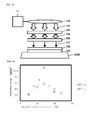
- FIG. 1 is a cross section view of the liquid crystal display element of the present invention.
- the substrate having the elements 100 to 105 is referred to as “back plane,” and the substrate having the with elements 200 to 205 is referred to as “front plane.”
- FIG. 2 illustrates processes of light exposure treatment using the pattern for producing the columnar spacers formed on the black matrix as a photo mask pattern.
- FIG. 3 is an illustrative exploded perspective view of an example of the liquid crystal display element of the present invention.
- FIG. 4 is a plan view enlarging the area surrounded by line II on the electrode layer 3 formed on the substrate 2 shown in FIG. 3 .
- FIG. 5 is a cross section view obtained by cutting the liquid crystal display element shown in FIG. 1 at line III-III shown in FIG. 4 .
- FIG. 6 is a plan view of another example enlarging the area surrounded by line II on the electrode layer 3 formed on the substrate 2 shown in FIG. 3 .
- FIG. 7 is a cross section view of another embodiment of the liquid crystal display element shown in FIG. 1 at line III-III shown in FIG. 4 .
- FIG. 8 is a cross section view of the liquid crystal display element as a color-on-filter.
- FIG. 9 is a cross section view of another example of the liquid crystal display element as a color-on-filter.
- FIG. 10 is a conception diagram showing the manufacturing method of the alignment film of the present invention.
- FIG. 11 is a view showing a relationship between the temperature of the polarized light irradiation time and the anchoring energy.
- the first aspect of the present invention is a method for manufacturing a liquid crystal alignment film, comprising: a process (I) of mixing a solvent with a photoresponsive polymer to prepare a photoresponsive polymer solution; a process (II) of coating the photoresponsive polymer solution on a substrate, followed by drying at 50 to 100° C. for 1 to 3 minutes and then drying at 120° C. to 180° C. for 5 to 75 minutes to form a coating; and a process (III) of adjusting a temperature of the coating film while the coating film is irradiated with a light of 200 to 350 nm at 40° C. to 100° C.
- the process (I) is to mix a solvent with a photoresponsive polymer to prepare a photoresponsive polymer solution.
- the solvent used in the present invention is not particularly limited, so long as it can dissolve a photoresponsive polymer. It can be appropriately selected depending on the property of the photoresponsive polymer to be used.
- the examples can include a lactone type such as ⁇ -butyrolactone; a ketone type such as cyclopentanone, cyclohexanone, MEK and MIBK; an ester type such as propylene glycol monomethyl ether acetate, and NMP (N-methyl-2-pyrrolidone).
- a solvent such as 2-methoxyethanol, 2-butoxy ethanol (butylcellosolve), and a toluene type such as toluene can be added to the solvent, if necessary.
- the photoresponsive polymer of the present invention is preferably selected from the group consisting of a photoresponsive decomposition type polymer, a photoresponsive dimerization type polymer, and a photoresponsive isomerization type polymer.
- the photoresponsive dimerization type polymer that can form a crosslinked structure by dimerization between side chains in response to light it is preferable to possess a high light sensitivity and a large orientation characteristic.
- the photoresponsive dimerization type polymer of the present invention can be preferably a compound represented by general formula (I) and/or (II).
- L represents a group derived from a polymerizable group
- Sp is a spacer group, that is, a divalent connection group selected from the group consisting of single bond, —(CH 2 ) u — (In the formula, u represents 1 to 20), —OCH 2 —, —CH 2 O—, —COO—, —OCO—, —CH ⁇ CH—, —CF ⁇ CF—, —CF 2 O—, —OCF 2 —, —CF 2 CF 2 — and —C ⁇ C—, wherein in these substituents, one or more of noncontiguous CH 2 groups therein can be independently replaced with —O—, —CO—, —CO—O—, —O—CO—, —Si(CH 3 ) 2 —O—Si(CH 3 ) 2 —, —NR—, —NR—CO—, —CO—NR—, —NR—CO—O
- A represents a structure selected from the group consisting of trans-1,4-cyclohexylene group (in the group, one methylene group, or two or more methylene groups not adjacent to each other, can be substituted with —O—, —NH— or —S—), 1,4-phenylene group (in the group, one or more groups of —CH ⁇ can be substituted with —N ⁇ ), 1,4-cyclohexenylene group, 2,5-thiophenylene group, 2,5-furanyl group, 1,4-bicyclo(2.2.2)octylene group, naphthalene-1,4-diyl group, naphthalene-2,6-diyl group, decahydronaphthalene-2,6-diyl group and 1,2,3,4-tetrahydronaphthalene-2,6-diyl group, wherein the functional group can be unsubstituted, or at least one of the hydrogen atoms thereof can be substituted with fluorine
- s represents an integer of 0 to 4, wherein when s represents 2 to 4, A and/or Q exist in plural, which can be the same as or different from each other;
- X and Y independently represents hydrogen atom, fluorine atom, chlorine atom, cyano group or an alkyl group having a carbon atom number of 1 to 20, wherein the hydrogen atom existing in the alkyl group can be substituted with fluorine atom, wherein when there is in the alkyl group one methylene group, or two or more methylene groups not adjacent to each other,
- said one methylene group, or said two or more methylene groups not adjacent to each other can be replaced with —O—, —CO—O—, —O—CO— or —CH ⁇ CH—;
- M represents general formula (IIa) below, general formula (IIb) below, or general formula (IIc) below.
- each of R 11 and R 12 represents hydrogen atom or an alkyl group with a carbon atom number of 1-30, independently, when there is one methyl group, or are two or more methyl groups not adjacent to each other, in the R 11 and R 12 , said one methyl group, or said two or more methyl groups not adjacent to each other can be substituted with —O—, —CO—, —CO—O—, —O—CO—, —CO—NH—, —NH—CO—, —NCH 3 —, —CH ⁇ CH—, —CF ⁇ CF— or —C ⁇ C—, the hydrogen atom in R 11 and R 12 can be substituted with alkyl group with a carbon atom number of 1-20, cyano group or halogen atom;
- each of ring C 1 , ring C 2 and ring C 3 independently represents:
- trans-1,4-cyclohexylene group in the group, one methyl group or two or more methyl groups not adjacent to each other can be substituted with —O—, —NH— or —S—),
- (C) a group selected from the group consisting of the 1,4-cyclohexenylene group, 2,5-thiophenylene group, 2,5-furanyl group, 1,4-bicyclo(2.2.2)octylene group, naphthalene-1,4-diyl group, naphthalene-2,6-diyl group, decahydronaphthalene-2,6-diyl group and 1,2,3,4-tetrahydronaphthalene-2,6-diyl group,
- the group (a), the group (b) and the group (c) as mentioned above can be unsubstituted, or one or more hydrogen atom can be substituted with fluorine atom, chlorine atom, cyano group, methyl radical, methoxy group or ethoxy groups,
- each of Z 1a and Z 1b independently represents a single bond, —(CH 2 ) v —, —O—, —CO—, —CO—O—, —O—OC—, —NR 7 —, —CO—NR 7 —, —NR 7 —CO—, —(CH 2 ) u —O—, —O—(CH 2 ) u —, —(CH 2 ) u —NR 7 or —NR 7 (CH 2 ) u —, and in this case, R 7 represents hydrogen atom or a lower alkyl group, v represents an integer of 1-4, u represents an integer of 1-3, and
- each of i and j represents 0 or 1.
- the group Sp is more preferably an alkylene oxide group having a carbon atom number of 6 to 12, or —(CH 2 ) m — (where m represents an integer of 8 to 12).
- said group derived from the polymerizable group is selected from the group consisting of groups derived from polymerizable groups represented by the following general formulae (III-1) to (III-11).
- R 30 represents hydrogen atom, fluorine atom, chlorine atom, an alkyl group having a carbon atom number of 1 to 4, phenyl group or phenoxy group;
- R 31 represents hydrogen atom, chlorine atom, methyl group or phenyl group
- R 32 each independently represents hydrogen atom or an alkyl group with a carbon atom number of 1 to 5.).
- photoresponsive dimerization type polymer can be substituted with the general formula (1) below:
- Sp is a spacer group, that is, a divalent connection group selected from the group consisting of single bond, —(CH 2 ) u — (In the formula, u represents 1 to 20), —OCH 2 —, —CH 2 O—, —COO—, —OCO—, —CH ⁇ CH—, —CF ⁇ CF—, —CF 2 O—, —OCF 2 —, —CF 2 CF 2 — and —C ⁇ C—, wherein in these substituents, one or more of noncontiguous CH 2 groups therein can be independently replaced with —O—, —CO—, —CO—O—, —O—CO—, —Si(CH 3 ) 2 —O—Si(CH 3 ) 2 —, —NR—, —NR—CO—, —CO—NR—, —NR—CO—O—, —O—CO—NR—, —NR—CO—NR—, —NR—CO—O—,
- Z 1 , Z 2 and Z 3 are each independently a single bond, —(CH2)u- (In the formula, u represents 1 to 20.)
- X represents —O—, —NR— or phenylene group
- Rb represents a polymerizable group, an alkoxy group, cyano group, or a fluorinated alkyl group having a carbon number of 1 to 12;
- n 0, 1 or 2;
- Mb and Md are each independently the same as or different from each other, and represented by a monomer unit of either one kind of the following general formulae (U-1) to (U-13).
- R a independently represents hydrogen atom, an alkyl group having a carbon atom number of 1 to 5, phenyl group, and halogen atom, wherein any hydrogen atom in each structure can be substituted with fluorine atom, chlorine atom, methyl group, phenyl group, methoxy group;
- the dashed line represents a bond connecting to Sp
- R 1 represents a tetravalent ring structure
- R 2 represents a trivalent organic group
- R 3 represents hydrogen atom, hydroxyl group, an alkyl group having a carbon atom number of 1 to 15, and an alkoxy group having a carbon atom number of 1 to 15.
- y and w represent a molar fraction of a copolymer, and are 0 ⁇ y ⁇ 1 and 0 ⁇ w ⁇ 1;
- n 4 to 100,000
- the monomer unit of Mb and Md each can be composed of one kind or two different kinds of units). It is preferably a polymer, a hydrolysate thereof, or a condensate of the hydrolysate thereof.
- the monovalent organic group can be represented by general formula (VII):
- Z 4 , Z 5 , Z 6 and Z 7 are each independently a single bond, —(CH 2 ) u — (In the formula, u represents 1 to 20.), —OCH 2 —, —CH 2 O—, —COO—, —OCO—, —CH ⁇ CH—, —CF ⁇ CF—, —CF 2 O—, —OCF 2 —, —CF 2 CF 2 — or —C ⁇ C—, wherein in these substituents, one or more of noncontiguous CH 2 groups therein can be independently replaced with —O—, —CO—, —CO—O—, —O—CO—, —Si(CH 3 ) 2 —O—Si(CH 3 ) 2 —, —NR—, —NR—CO—, —CO—NR—, —NR—CO—O—, —O—CO—NR—, —NR—CO—CO—NR—, —NR—CO—O—, —O—
- r1, s1, t1 and u1 each independently represents 0 or 1;
- R 12 represents hydrogen, fluorine, chlorine, cyano group or an alkyl group having a carbon number of 1 to 20, wherein the hydrogen atom in the alkyl group can be substituted with fluorine atom, wherein one CH 2 group or non-adjacent two or more CH 2 groups can be substituted with —O—, —CO—O—, —O—CO— and/or —CH ⁇ CH—.).
- a preferable embodiment of the photoresponsive dimerization type polymer represented by the general formula (1) of the present invention above is preferably a polymer in which Z 2 is a single bond.
- photoresponsive dimerization type polymer represented by general formula (1) of the present invention can be preferably represented by general formula (2) below:
- R 21 to R 24 are each independently hydrogen atom, or an alkoxy group having a carbon atom number of 1 to 5;
- W represents hydrogen atom, fluorine atom, methyl group, methoxy group, ethyl group or ethoxy group, W represents at least one kind selected from the group consisting of general formulae (W-1) to (W-8).
- W is a group represented by (W-1).
- each of the alkyl group and the alkoxy group of the present invention is linear, cyclic or branched, and in particular, it is further preferable that it is linear or branched.
- the examples of the “alkyl group” of the present invention can include methyl group, ethyl group, propyl group, butyl group, isopropyl group, isobutyl group, t-butyl group, 3-pentyl group, isopentyl group, neopentyl group, pentyl group, hexyl group, heptyl group, and octyl group.
- the examples of the alkyl group are common, and can be appropriately selected from the examples as mentioned above in accordance with the carbon atom number of each alkyl group.
- the example of the “alkoxy group” of the present invention is a group in which oxygen atom is directly connected to an alkyl group.
- the examples can preferably include methoxy group, ethoxy group, propoxy group (n-propoxy group, i-propoxy group), butoxy group, pentyloxy group, and octyloxy group.
- the examples of the alkoxy group are common, and can be appropriately selected from the examples as mentioned above in accordance with the carbon atom number of each alkoxy group.
- a favorable embodiment of the manufacturing method of liquid crystal alignment film of the present invention is as follows. That is, it is a method for manufacturing a liquid crystal alignment film, comprising:
- the dimerization of the polymer is particularly promoted, the effect of improvement of the anchoring power can be obtained. Therefore, as the photoresponsive polymer of the present invention, a photoresponsive dimerization type polymer is particularly preferable.
- the light to be used for the dimerization between side chains is preferably of 200 to 350 nm; in particular, it is more preferably of 250 to 350 nm; it is further preferable to be 250 to 330 nm.
- the photoresponsive decomposition type polymer of the present invention is prepared by condensation between tetracarboxylic dianhydride and a diamine compound.
- the tetracarboxylic dianhydride above can include the formulae (A-1) to (A-43) below.
- the diamine compound can include the formulae (III-1) to (VIII-17).
- R1 to R10 are primary amino group, and the remainders are hydrogen atom or monovalent organic group other than primary amino group, and they are the same as or different from each other.
- diamine compounds having a cinnamic acid frame as the above formulae (1) to (5) can be dimerized in response to light, so that they are preferably used as the photoresponsive dimerization type polymer.
- the light to be used for the cutting the molecular chain is preferably of 200 to 400 nm; in particular, it is more preferably of 200 to 280 nm; it is further preferable to be 240 to 280 nm.
- the photoresponsive isomerization type polymer of the present invention can be prepared by synthesis of tetracarboxylic dianhydride with a diamine compound, and that at least one of the tetracarboxylic dianhydride and the diamine has a diazo bond.
- the tetracarboxylic dianhydride having a diazo bond can include the compound represented by following formula (1-8).
- diamine having a diazo bond can include the following formulae (I-1) to (I-7):
- a compound as a diamine having a diazo bond is selected from the formulae (I-1) to (I-7)
- a compound as the tetracarboxylic dianhydride is from the groups represented by formula (1-8) and formulae (A-1) to (A-43).
- a compound selected as the tetracarboxylic dianhydride having a diazo bond is formula (1-8)
- a compound as the diamine compound is selected from the compounds represented by formulae (I-1) to (I-7) and formulae (III-1) to (VIII-11), (I) and (1) to (5).
- the light to be used when isomerized in response to light and oriented in nearly vertical direction with respect to the polarization axis is preferably of 200 to 500 nm; in particular, it is more preferably of 300 to 500 nm; it is further preferable to be 300 to 400 nm.
- the weight average molecular weight of the photoresponsive decomposition type polymer of the present invention is preferably 3,000 to 30,000; it is more preferably 5,000-100,000; it is more preferable 10,000-50,000; and specifically, it is more preferably 10,000-30,000.
- the weight average molecular weight of the photoresponsive isomerization type polymer of the present invention is preferably 10,000 to 800,000; it is more preferably 10,000-400,000; it is yet more preferably 50,000-400,000; and in particular, it is more preferably 50,000-300,000.
- the weight average molecular weight of the photoresponsive dimerization type polymer of the present invention is preferably 5,000 to 800,000; it is more preferably 6,000-400,000; it is yet more preferably 100,000-400,000; and in particular, it is more preferably 100,000-300,000.
- the weight average molecular weight (Mw) as mentioned above are obtained by a measurement result of GPC (gel permeation chromatography).
- the concentration of the photoresponsive polymer solution of the present invention is preferably 1 to 20 mass %; and more preferably 2-10 mass %; and yet more preferably 2 to 5 mass %.
- the process (II) of the present invention is to coat the photoresponsive polymer solution on a substrate, followed by drying at 50 to 100° C. for 1 to 3 minutes and then drying at 120° C. to 180° C. for 5 to 75 minutes to form a coating.
- the average thickness of the coating film of the present invention is 1 to 1,000 nm; and in particular, it is more preferable that it is 5 to 500 nm; and it is further preferable that it is 10 to 200 nm; and it is yet further preferable that it is 20 to 90 nm.
- the method for measurement of the average thickness of the coating film of the present invention is a measurement of difference in level by using a contact type film thickness meter which is carried out after the application of light alignment film and the light irradiation. Also, the method for measuring the average film thickness of the liquid crystal alignment film obtained by the manufacturing method of the present invention is the same.
- the substrate to be used in present invention is preferably a transparent substrate.
- a transparent substrate Considering the relationship with the solvent used for the photoresponsive polymer solution, so long as it is a material that does not dissolve in the solvent, it is not particularly limited.
- the example thereof can include glass substrate or quartz substrate.
- the coating method of the present invention can include spin coat method, bar coating method, flexographic printing method, and ink-jet method.
- the drying method of the coating film of the present invention can include heat drying and vacuum drying.
- the dry condition of the present invention is as follow. It is preferable to heat at 20 to 150° C. for 0.1 to 20 minutes followed by heating at 80° C. to 250° C. for 1 to 100 minutes; or it is preferable to heat at 30 to 120° C. for 0.5 to 10 minutes followed by heating at 100° C. to 200° C. for 2 to 90 minutes; or it is preferable to heat at 50 to 100° C. for 1 to 3 minutes followed by heating at 120° C. to 180° C. for 5 to 75 minutes; or it is preferable to heat at 70 to 90° C. for 2 to 3 minutes followed by drying at 150° C. to 180° C. for five minutes.
- the number of drying of the coating film of the present invention it is preferable to do one time or more and five times or less. It is more favorable to do one time or more and three times or less.
- the process (III) of the present invention to adjust the temperature of the coating film at 40° C. to 100° C. while irradiating light of 200 to 350 nm.
- the manufacturing method of the present invention by adjusting the temperature of the coating film at the time of the light irradiation, it is considered that the change of the molecular structure is promoted such that the effect of improvement of the anchoring power can be exhibited.
- the photoresponsive dimerization type polymer as mentioned above is used as the photoresponsive polymer, it has been found that the dimerization can be promoted by controlling the temperature of the coating film at a specific range at the time of the light irradiation.
- the method to adjust the temperature of the coating film is preferably performed by employing a maintenance means, e.g., by heating on a hot plate or applying polarized light irradiation inside a constant temperature bath.
- a process (III) it is preferable to irradiate the coating film with light of 200 to 350 nm in a state where the temperature of the coating film is maintained at 38° C. to 110° C.; and it is further preferable to irradiate the coating film with light of 230 to 340 nm in a state where the temperature of the coating film is maintained at 40° C. to 100° C.; and it is yet further preferable to irradiate the coating film with light of 250 to 330 nm in a state where the temperature of the coating film is maintained at 50° C. to 90° C.; it is particularly preferable to irradiate the coating film with light of 270 to 330 nm in a state where the temperature of the coating film is maintained at 65° C. to 75° C.
- the light irradiation in the process (III) to of the present invention can give the coating film a liquid crystal orientation ability.
- ultraviolet rays and visible rays including light having a wavelength of 150 nm to 800 nm can be employed.
- the light to be irradiated can be polarized light or unpolarized light.
- polarized light it can be linear polarized light or partially polarized light.
- the term “unpolarized light” shall include light that is partly polarized, if it is substantially unpolarized light.
- the light to irradiate the coating film in the process (III) of the present invention is preferably linear light, and also it is more preferable that it is linear polarized light.
- the irradiation can be performed from the direction perpendicular to the substrate surface, or alternatively it can performed from a slant direction in order to give a pretilt angle, or a combination of both can be performed.
- the irradiation direction is required to be a slant direction.
- pretilt angle in the specification of the present application means an angle of the inclination of the liquid crystal molecule from the direction parallel to the substrate surface.
- the example thereof can include low pressure mercury lamp, high pressure mercury lamp, super high pressure mercury lamp, deuterium lamp, metal halide lamp, argon resonance lamp, xenon lamp, excimer laser mercury xenon lamp (Hg—Xe lamp).
- the ultraviolet rays of linear polarized light or partially polarized light is preferably provided by means of e.g., using a light source thereof along with a filter, a diffraction grating, and etc.
- An exposure dose of the light in the present invention is preferably 1 mJ/m 2 to 1,000 mJ/m 2 ; it is more preferable that it is 5 mJ/m 2 to 1,000 mJ/m 2 ; and it is further preferable that it is 10 mJ/m 2 to 500 mJ/m 2 ; and it is specifically preferable that it is 10 mJ/m 2 to 100 mJ/m 2 .
- a liquid crystal orientation ability is given to a coating film formed from a liquid crystal orientation agent by means of a light orientation method as conventionally known, a light exposure doses of more than about 1,000 mJ/m 2 is required.
- the manufacturing method of the present invention it is possible to reduce the light exposure dose at the light orientation method to a level of 10 to 100 mJ/m 2 or less. Therefore, good liquid crystal orientation ability can be given with production cost saving.
- the yellowing of the orientation film through the light irradiation can be decreased, as well.
- the liquid crystal molecule is oriented in nearly horizontal direction with respect to the substrate.
- a horizontal electric field type liquid crystal display element such as FFS mode and IPS mode as described later
- an anchoring effect can be evenly and uniformly given even to such a horizontal electric field type liquid crystal display element which has an electrode structure with a number of surface irregularities.
- the orientation can be uniform without defects, thereby increasing a contrast.
- a particularly preferable embodiment of the process (III) of the present invention is to irradiate the substrate of the present invention with a linear light of 200 to 350 nm from nearly a vertical direction thereof at a condition that the exposure dose of the linear polarized light is 10 to 100 mJ/cm 2 .
- the substrate As the light irradiation from nearly vertical direction above, it is preferable to irradiate the substrate from the direction at an angle of 70 to 110 degrees.
- the second aspect of the present invention is a method of orientating a liquid crystal composition, comprising: a process (I) of mixing a solvent with a photoresponsive dimerization polymer to prepare a photoresponsive dimerization polymer solution, the photoresponsive dimerization polymer forming a crosslinked structure by dimerization between side chains in response to light; a process (2) of forming a coating film of the photoresponsive dimerization polymer solution on surfaces of a first substrate and a second, followed by drying at 50 to 100° C. for 1 to 3 minutes and then drying at 120° C. to 180° C.
- the third aspect of the present invention is a liquid crystal display element provided with the liquid crystal alignment film of the present invention.
- the examples useful can include ECB-LCD, VA-LCD, VA-IPS-LCD, FFS-LCD, TN (nematic liquid crystal display element), STN-LCD (super twisted nematic liquid crystal display element), OCB-LCD and IPS-LCD (in-plane switching liquid crystal display element), but it is particularly useful for FFS-LCD, IPS-LCD, and can be used as a transmission type or reflection type liquid crystal display element.
- Two substrates of a liquid crystal cell used in the liquid crystal display element can be made of transparent material having flexibility, such as glass or resin material, and one of the substrates may be made of opaque material such as silicon.
- a transparent substrate having a transparent electrode layer can be made by, for example, sputtering indium tin oxide (ITO) on a transparent substrate such as a glass plate.
- the color filter can be produced by, for instance, a pigment dispersion method, a printing method, an electrodeposition method, or a staining method.
- a production method of a color filter by a pigment dispersion method is explained here.
- a curable color composition used for a color filter is coated on the transparent substrate, and subject to a pattering treatment, which is then cured by heating or photo irradiation. This process is carried out with respect to each of three colors, i.e., red, green and blue, thereby forming pixels of the color filter.
- the surface of the substrate can be provided with an active element such as a TFT and thin-film diode, serving a pixel electrode.
- the substrates are arranged such that the transparent electrode layers are disposed inside (i.e., such that the liquid crystal alignment films face each other).
- a spacer can be disposed to adjust the distance between the substrates.
- the thickness of a light modulating layer (i.e., liquid crystal layer) as obtained is in a range of 1-100 ⁇ m. It is further preferable that it is in a range of 1.5 to 10 ⁇ m.
- the spacer can include a columnar spacer made of, for instance, glass particles, resin particles, alumina particles and photoresist materials.
- liquid crystal composition which can further include a polymerizable compound, if necessary
- a general method such as a vacuum injection method and an ODF method can be used.
- a vacuum injection method although drop marks are not generated, this method has a problem in that an mark at the injection is left.
- it can be further preferable when using the ODF method to produce a liquid crystal composition.
- a sealing material such as an optically thermally curable epoxy based material is applied to either one substrate of the back plane and the front plane by using a dispenser such that a wall in a shape of a closed loop is drawn, into which a certain amount of the liquid crystal composition is dropped under a vacuum condition, thereby bonding the front plane with the back plane to manufacture a liquid crystal display element.
- a dispenser such that a wall in a shape of a closed loop is drawn, into which a certain amount of the liquid crystal composition is dropped under a vacuum condition, thereby bonding the front plane with the back plane to manufacture a liquid crystal display element.
- the liquid crystal display element using the liquid crystal composition of the present invention is useful in accomplishing both the high speed response and the restraint of the display defectiveness. It is particularly useful for a liquid crystal display element of active matrix driving, and applicable to liquid crystal display elements of VA mode, PSVA mode, PSA mode, IPS (in-plane switching) mode, VA-IPS mode FFS (fringe field switching) mode and ECB mode.
- liquid crystal display element of the present invention i.e., one example of liquid crystal display
- FIG. 1 is a cross-sectional view of a liquid crystal display element including two substrates opposed to each other, a sealing material disposed between the substrates, and liquid crystal confined in the sealed region surrounded by the sealing material.
- FIG. 1 illustrates an embodiment of a liquid crystal display element which includes a back plane in which a first substrate 100 is provided with TFT layers 102 and pixel electrodes 103 formed thereon, onto which a passivation film 104 and a first alignment film 105 are provided; a front plane opposed to the back plane, the front plane including a second substrate 200 which is provided with a black matrix 202 , a color filter 203 , a planarization film (overcoat layer) 201 , and transparent electrode 204 , onto which a second alignment layer 205 is provided; a sealing material 301 disposed between the substrates; and a liquid crystal layer 303 confined in a sealed region surrounded by the sealing material, in which the substrate surface contacting the sealing material 301 is provided with protrusions (columnar spacer) 302 , 303 .
- the resin substrate can include cellulose and cellulose derivative such as triacetylcellulose and diacetyl cellulose; polycycloolefin derivative, polyester such as polyethylene terephthalate and polyethylenenaphthalate; polyolefin such as polypropylene and polyethylene; polycarbonate, polyvinyl alcohol, polyvinyl chloride, polyvinylidene chloride, polyamide, polyimide, polyimide amide, polystyrene, acrylics, polymethyl methacrylate, polyethersulfone, and polyarylate, and furthermore, inorganic-organic composite material such as fiberglass-epoxy resin, fiberglass-acrylic resin.
- cellulose and cellulose derivative such as triacetylcellulose and diacetyl cellulose
- polycycloolefin derivative polyester such as polyethylene terephthalate and polyethylenenaphthalate
- polyolefin such as polypropylene and polyethylene
- polycarbonate polyvinyl alcohol, polyvinyl chloride, polyvinylid
- a barrier film is preferably provided.
- the barrier film serves to reduce the moisture permeability of the resin substrate, thereby improving the reliability of the electric properties of the liquid crystal display element.
- any material having high transparency and low water vapor permeability can be used.
- it can be a thin film formed from an inorganic material such as silicon oxide by means of vapor deposition, sputtering, or a chemical vapor deposition method (CVD method).
- the first substrate and the second substrate can be made of the same material as, or different material from each other, and there is no specific limitation.
- a glass substrate is preferable since a liquid crystal display element with excellent thermal resistance and dimensional stability can be produced.
- a resin substrate is preferable since it is suitable for a manufacturing method through a roll-to-roll process, and appropriate to accomplish the improvements of light weight and flexibility. Also, if focusing on imparting flatness and thermal resistance, a combination of a resin substrate and a glass substrate can bring good results.
- a glass substrate is used as the first substrate 100 or the second substrate 200 .
- the first substrate 100 is provided with TFT layers 102 and pixel electrodes 103 thereon. These components are formed through an array process which is generally used. Onto this, the passivation film 104 and the alignment film 105 are formed to obtain the back plane.
- the passivation film 104 (which is also called as an inorganic protective film) is a film to protect the TFT layers. Generally, it is a nitride film (SiNx), an oxide film (SiOx) and etc. formed by means of a chemical vapor deposition (CVD) technique.
- SiNx nitride film
- SiOx oxide film
- CVD chemical vapor deposition
- the first liquid alignment film 105 and the second liquid alignment film 205 are the films serving to align the liquid crystal molecules obtained by the manufacturing method of the liquid crystal alignment film of the present invention.
- the alignment film can deteriorate the adhesion of the sealing material to the alignment film so that it is coated in a pattern inside the sealed region.
- a group which causes a photo reaction bringing about the liquid crystal alignment (which is hereinafter referred to as photo alignment group) can be used, which can include molecule alignment inducement by means of Weigert's effect due to photodichroism (isomerization reaction) (e.g., azobenzene group), a dimerization reaction (e.g., cinnamoyl group), or a photolysis reaction (e.g., polyimide group).
- photo alignment group can include molecule alignment inducement by means of Weigert's effect due to photodichroism (isomerization reaction) (e.g., azobenzene group), a dimerization reaction (e.g., cinnamoyl group), or a photolysis reaction (e.g., polyimide group).
- photo alignment group e.g., azobenzene group
- dimerization reaction e.g., cinnamoyl group
- a photolysis reaction e.g., polyimi
- an alignment film After the coated alignment agent solution is temporarily dried to evaporate the solvent, it is preferable that by controlling the temperature of the coating film when the product is irradiated with light having a certain polarization (polarized light), an alignment film can be provided with an alignment ability in any direction.
- polarized light polarized light
- the black matrix 202 there are the black matrix 202 , the color filter 203 , the planarization film 201 , the transparent electrode 204 , and the second alignment film 205 formed on the second substrate 200 .
- the black matrix 202 is formed by, for example, a pigment dispersion method.
- a color resin liquid in which a black colorant has been uniformly dispersed for the purpose of forming the black matrix, thereby forming a colored layer.
- the colored layer is cured by baking.
- a photoresist is applied onto the cured layer and then subject to a preliminary baking. The photoresist is exposed to light through a mask pattern, and then, developed to make pattern the colored layer. Then, the photoresist layer is removed, and the colored layer is baked to complete the formation of the black matrix 202 .
- a photoresist type pigment dispersion liquid can be used.
- a photoresist type pigment dispersion liquid is applied and preliminarily baked, which is followed by being exposed with light through a mask pattern, and then developed to pattern the colored layer. Then, the photoresist layer is removed, and the colored layer is baked to complete the formation of the black matrix 202 .
- the color filter 203 is formed by means of a pigment dispersion method, an electrodeposition method, a printing method, or a staining method.
- a pigment dispersion method for example, a color resin solution in which a pigment (e.g., red) has been uniformly dispersed is applied onto the second substrate 200 and then cured by baking, onto which a photoresist is applied and preliminarily baked.
- the photoresist is exposed with light through a mask pattern, then developed, to carry out patterning. Then, the photoresist layer is removed, and it is baked again, thereby completing the formation of a (red) color filter 203 .
- the color filters can be formed in any order with respect to the colors. In the same manner, a green color filter 203 and a blue color filter 203 are formed.
- the transparent electrode 204 is formed on the color filter 203 (if necessary, the overcoat layer ( 201 ) is optionally formed on the color filter 203 to flatten a surface).
- the transparent electrode 204 preferably has a higher light transmittance and lower electric resistance.
- an oxide film of, for example, ITO is formed by sputtering.
- a passivation film can be formed on the transparent electrode 204 in some cases.
- the second alignment film 205 is the same as the first alignment film 105 as mentioned above.
- the present invention is not limited to the specific embodiment.
- the change of the embodiment depending on a desired liquid crystal display element can be freely made.
- the shape of the columnar spacer is not limited, and can have any shape.
- its horizontal cross section can have any shape such as a circular, a rectangular or a polygonal shape.
- its horizontal cross section preferably has a shape of a circular or a regular polygonal shape in view of margin for misalignment in the production process.
- the protrusions preferably have a shape of truncated cone or truncated pyramid.
- the material of the columnar spacer is not specifically limited, so long as it is insoluble in the sealing material, an organic solvent used in the sealing material, or the liquid crystal.
- it can be preferably a synthetic resin (curable resin).
- the protrusion can be provided on a surface of the first substrate where it contacts the sealing material by means of a photolithography method or a droplet ejection method.
- a photocurable resin which is suitable for the photolithography method and the droplet ejection method can be preferably used.
- FIG. 2 illustrates processes of light exposure treatment using the pattern for producing the columnar spacers formed on the black matrix as a photo mask pattern.
- a resin solution (which does not contain a colorant) used for forming the columnar spacer is coated on the transparent electrode 204 of the front plane. Then, this resin layer 402 is cured by baking. There, a photoresist is coated and then preliminarily baked. The photoresist is exposed with light through a mask pattern 401 , and then developed to make a patterning of the resin layer. Then, the photo resist layer is removed, and then, the resin layer is baked to finish the formation of the columnar spacer ( 302 , 303 of FIG. 1 ).
- a position to form the columnar spacers can be determined as needed depending on the mask pattern. Therefore, both the inside of the sealed region of the liquid crystal display element and the outside thereof (the part where the sealing material is applied) can be simultaneously formed. Also, it is preferable that the columnar spacers are formed above the black matrix to avoid the deterioration of the quality of the sealed region.
- the columnar spacers formed through the photolithography method as explained above can be sometimes called as column spacer or photo spacer.
- a mixture can be used, which contains, for example, a negative water-soluble resin, such as a PVA-stilbazo photosensitive resin, a polyfunctional acrylic monomer, an acrylic acid copolymer, and a triazole-based initiator.
- a color rein is used, in which a colorant has been dispersed in a polyimide resin.
- the spacer can be prepared by using known material which is suitable with the liquid crystal and the sealing material.
- the columnar spacers are formed on the surface of the front plane where it becomes a sealed region, before the sealing material (represented by the symbol 301 in FIG. 1 ) is coated on the surface of the back plane where the seal material contacts.
- the material of the sealing material is not particularly limited.
- a curable resin composition can be used which is prepared by adding a polymerization initiator to an epoxy-based or acrylic-based photocurable resin, thermosetting resin, or optically and thermally curable resin.
- fillers made of an inorganic or organic material can be added in some cases to adjust moisture permeability, elastic modulus, and viscosity. Such fillers may have any shape such as spherical shape, fibrous shape, or amorphous shape.
- a spherical or fibrous gap material having a single dispersion diameter can be mixed to favorably control the cell gap, and a fibrous material which can be easily entangled around the protrusion formed above the substrate can be mixed to enhance the adhesion to the plates. It is desirable that the diameter of the fibrous material used in this case is less than around 1 ⁇ 5 to 1/10 of the cell gap, and the length of the fibrous material is preferably shorter than the coating width of the sealing material.
- the material of the fibrous material is not particularly limited so long as a predetermined shape can be obtained. It can be appropriately selected from synthetic fibers such as cellulose, polyamide, and polyester, and inorganic materials such as glass and carbon.
- the sealing material it can be coated by means of a printing method or a dispensing method, but a dispensing method is prefer because of using a small amount of the sealing material.
- the position to coat the sealing material is set above the position of the black matrix in order to avoid adversely affecting the sealed region.
- the shape of the sealing material is a closed loop.
- a liquid crystal is dropped at the closed loop structure (sealed region) of the front plane, the closed loop structure having been formed by application of the sealing material.
- a disperser is used. Since the amount of the liquid crystal to be dropped should be equivalent to the capacity of the liquid crystal cell, the amount is basically equal to the volume that is the product of the height of the columnar spacer and the coated area of the sealing material. However, in order to reduce the leakage of the liquid crystal during the cell bonding process or optimize the display characteristics, the amount of the liquid crystal to be dropped can be appropriately adjusted, or the positions to which the liquid crystal are dropped can be dispersed.
- the back plane is bonded to the front plane in which the sealing material has been coated and the liquid crystal has been dropped.
- the front plane and the back plane are attached to a stage having a mechanism for holding a substrate, such as an electrostatic chuck, and then the front plane and the back plane are disposed at a position (in a distance) such that the second alignment film of the front plane is opposed to the first alignment film of the back plane while the sealing material does not contact the other substrate.
- pressure in the system is reduced.
- the positions of the front plane and back plane are adjusted while the bonding parts of the front plane and the back plane are being checked (alignment process).
- the substrates are moved close to each other to a position at which the sealing material on the front plane contacts the back plane.
- the inside of the system is filled with inert gas, and the vacuum is gradually reduced and returned to normal pressure.
- atmospheric pressure enables the front plane and the back plane to be bonded to each other, so as to create a cell gap with the height of the columnar spacers.
- the sealing material is irradiated with ultraviolet light to cure the sealing material, thereby forming the liquid crystal cell.
- a heating process is optionally carried out to promote the curing of the sealing material. The heating process is carried out in many cases to enhance the adhesion of the sealing material and the reliability of electric properties.
- a second favorable embodiment of the liquid crystal display element of the present invention is a liquid crystal display element as follows.
- a first substrate having an electrode layer including a first alignment layer and a thin film transistor on the surface thereof, and a second substrate having a second alignment layer on the surface thereof are disposed such that these alignment layers face each other with a gap, and that a liquid crystal layer including a liquid crystal composition is filled between the first substrate and the second substrate.
- the electrode layer including the thin film transistor is preferably provided with a plurality of gate wirings and data wirings arranged in a mesh shape, a thin film transistor provided at each of the intersections of the data wirings and the gate wirings, a pixel electrode connected to the thin film transistor, and a common electrode provided on the first substrate, the common electrode separated from the pixel electrode.
- the first alignment layer and the second alignment layer provided close to the liquid crystal layer are preferably alignment films which induce a homogeneous alignment with respect to the liquid crystal composition.
- the liquid crystal display element above preferably has a structure in which a second polarizing plate, a second substrate, an electrode layer including a thin film transistor (or which can be referred to as a thin film transistor layer), a liquid crystal alignment film obtained in accordance with the manufacturing method of the present invention, a liquid crystal layer including a liquid crystal composition, an alignment film, a color filter, a first substrate, and a first polarizing plate are stacked in order.
- the electric field (E) generated between the common electrode and the pixel electrode can be provided with a planar direction component. Therefore, for example, in a case where an alignment film which induces a homogeneous alignment with respect to the liquid crystal composition is used in the alignment layer, there can be provided an element as follows. Prior to applying a voltage between the common electrode and the pixel electrode, the liquid crystal molecules are arranged in the surface direction, that is, the alignment direction of the alignment film, to block the light; but when applying a voltage, the liquid crystal molecules are rotated horizontally due to the electric field (E) applied in the planar direction to be oriented along the electric field direction, so as to block the light.
- the form of the liquid crystal display element according to the present invention can be, so-called, a color filter-on-array (COA), and a color filter can be provided between the electrode layer including a thin film transistor and the liquid crystal layer, or a color filter can be provided between the electrode layer including the thin film transistor and the second substrate.
- COA color filter-on-array
- a state supported by a substrate that is, a state not only brought into direct contact, but also brought into indirect contact, with a substrate.
- More favorable another form of the second favorable embodiment of the liquid crystal display construction of the present invention is a liquid crystal display element as follows.
- a first substrate having an electrode layer including a first alignment layer and a thin film transistor on the surface thereof, and a second substrate having a second alignment layer on the surface thereof are disposed such that these alignment layers face each other with a gap, and that a liquid crystal layer including a liquid crystal composition is filled between the first substrate and the second substrate.
- the electrode layer including the thin film transistor is preferably provided with a plurality of gate wirings and data wirings arranged in a mesh shape, a thin film transistor provided at each of the intersections of the data wirings and the gate wirings, a pixel electrode connected to the thin film transistor, and a common electrode provided on the first substrate, the common electrode separated from the pixel electrode.
- the shortest distance d between the common electrode and the pixel electrode which are adjacent to each other is shorter than the shortest distance G between the alignment layers.
- a liquid crystal display element satisfying the condition that the shortest distance d between the common electrode and the pixel electrode is longer than the shortest distance G between the alignment layers is called as an IPS mode liquid crystal display element, and an element satisfying the condition that the shortest distance d between the common electrode and the pixel electrode which are adjacent is shorter than the shortest distance G between the alignment layers is called as FFS. Therefore, only the condition of the FFS mode is that the shortest distance d between the common electrode and the pixel electrode which are adjacent to each other is shorter than the shortest distance G between the alignment layers, and therefore, there is no limitation to the positional relationship in the thickness direction between the surface of the common electrode and the surface of the pixel electrode.
- the pixel electrode can be provided closer to the liquid crystal layer than the common electrode, or alternatively, the pixel electrode and the common electrode can be provided on the same plane.
- the photo alignment film according to the present invention is preferable when it is used in a liquid crystal display element of an FFS driving system (FFS-LCD) from the viewpoint of high speed response and reduction of burn-in.
- FFS-LCD FFS driving system
- FIG. 3 is an exploded perspective view schematically showing a structure of one embodiment of a liquid crystal display element, that is, so-called an FFS mode liquid crystal display element.
- the liquid crystal display element 10 according to the present invention preferably has a structure in which a second polarizing plate 8 , a second substrate 7 , an electrode layer 3 including a thin film transistor (or which is referred to as a thin film transistor layer), an alignment film 4 , a liquid crystal layer 5 including a liquid crystal composition, an alignment film 4 , a color filter 6 , a first substrate 2 , and a first polarizing plate are stacked in order. Also, as shown in FIG.
- the second substrate 7 and the first substrate 2 can be sandwiched between a pair of the polarizing plates 1 , 8 . Furthermore, in FIG. 3 , the color filter 6 is provided between the second substrate 7 and the alignment film 4 . Moreover, a pair of alignment films 4 which are adjacent to the liquid crystal layer 5 according to the present invention to bring into direct contact with the liquid crystal composition constructing the liquid crystal layer 5 can be formed on the (transparent) electrode (layer) 3 .
- liquid crystal display element 10 can be, so-called, a color filter-on-array (COA), and a color filter 6 can be provided between a thin film transistor 3 and a liquid crystal layer 5 , or a color filter 6 can be provided between the film transistor 3 and the first substrate 2 .
- COA color filter-on-array
- an FFS mode liquid crystal display element In the FFS mode liquid crystal display element, a fringe electric field is employed.
- a fringe electric field can be formed between the common electrode and the pixel electrode, such that the alignment in the horizontal direction and the vertical direction of the liquid crystal molecules can be efficiently used. Therefore, an FFS mode liquid crystal display element can employ an electric field in the horizontal direction, that is formed in the vertical direction with respect to the line of the pixel electrode 21 , the line forming a comb tooth shape, and an electric field of a parabolic shape.
- FIG. 4 is an enlarged plan view of a region II of the electrode layers 3 (or which is referred to as a thin film transistor layer 3 ) including the thin film transistor formed on the substrate in FIG. 3 .
- a thin film transistor 20 including a source electrode 27 , a drain electrode 24 and a gate electrode 28 is provided in connection with the pixel electrode 21 serving as a switching element in order to supply a display signal to the pixel electrode 21 .
- FIG. 4 shows an example having a structure in which a flat plate shaped common electrode 22 is formed on one surface with intervention of an insulating layer (not shown) on the back surface of the comb tooth shaped pixel electrode 21 .
- the surface of the pixel electrode 21 can be covered with a protective insulating film and an alignment film layer. It is noted that in the region surrounded by a plurality of the gate wirings 26 and a plurality of the data wirings 25 , a storage capacitor 23 can be provided to store a display signal supplied through the data wiring 25 . Furthermore, a common line 29 is provided in parallel with the gate wiring 26 . The common line 29 is connected to the common electrode 22 to supply common signal to the common electrode 22 .
- FIG. 5 is one example of a sectional view showing by cutting the liquid crystal display element in the direction of line III-III in FIG. 4 .
- the first substrate 2 having formed on its surface an alignment layer 4 and the electrode layer 3 including the thin film transistor 20 ( 11 , 12 , 13 , 14 , 15 , 16 , and 17 ), and the second substrate 7 having formed the alignment layer 4 on its surface are disposed such that the alignment layers face each other with a predetermined interval G.
- the liquid crystal layer 5 including a liquid crystal composition is filled.
- the gate insulating film 12 is formed on a part of the surface of the first substrate 2
- the common electrode 22 is formed on a part of the surface of the gate insulating film 12
- an insulating film 18 is further formed to cover the common electrode 22 and the thin film transistor 20 .
- the pixel electrode 21 is provided on the insulating film 18 , and the pixel electrode 21 is in contact with the liquid crystal layer 5 through the alignment layer 4 . Therefore, the minimum distance d between the pixel electrode and the common electrode can be adjusted as an (average) film thickness of the gate insulating film 12 . In other words, in the embodiment shown in FIG. 5 , the distance between the common electrode and the pixel electrode in the horizontal direction with respect to the substrate becomes 0.
- an electrode width 1 of the comb tooth shaped portion of the pixel electrode 21 and the gap width m of the comb tooth shaped portion of the pixel electrode 21 are formed in such an extent of the width that all the liquid crystal molecules in the liquid crystal layer 5 can be driven by the electric field generated.
- the liquid crystal molecules arranged in the surface direction which corresponds to the alignment direction of the alignment film can block the light; and when a voltage is applied, an electric field of a planar direction component is generated since the common electrode and the pixel electrode are provided on the same substrate (or an electrode layer) with a gap, and an electric field (fringe electric field) of a vertical direction component is generated as derived from the edge of these electrodes since the shortest distance d between the common electrode and the pixel electrode which are adjacent to each other is shorter than the shortest distance G between the alignment layers, and therefore, even liquid crystal molecules having a low dielectric anisotropy can be driven. Therefore, an amount of a compound having a high dielectric anisotropy ( ⁇ ) can be significantly reduced in the liquid crystal composition, so that the liquid crystal composition can contain a
- the alignment film obtained by the manufacturing method of the present invention can exhibit a high anchoring effect, so that there are many kinds of liquid crystal compositions that can be used. Therefore, even a liquid crystal composition having relatively a low dielectric constant, that can be used, can be driven.
- FFS liquid crystal display element favorably as follows.
- a first substrate having an electrode layer including a first alignment layer and a thin film transistor on the surface thereof, and a second substrate having a second alignment layer on the surface thereof are disposed such that these alignment layers face each other with a gap, and that a liquid crystal layer including a liquid crystal composition is filled between the first substrate and the second substrate.
- the electrode layer including the thin film transistor is preferably provided with a common electrode, a plurality of gate wirings and data wirings arranged in a mesh shape, a thin film transistor provided at each of the intersections of the data wirings and the gate wirings, a pixel electrode connected to the thin film transistor.
- the pixel electrode is protruded more than the common electrode at the side of the second substrate.
- the first alignment layer and the second alignment layer provided close to the liquid crystal layer are preferably alignment films which induce a homogeneous alignment with respect to the liquid crystal composition.
- FIG. 6 is another form of an enlarged plan view of a region II of the electrode layers 3 (or which is referred to as a thin film transistor layer 3 ) including the thin film transistor formed on the substrate in FIG. 3 .
- a thin film transistor 20 including a source electrode 27 , a drain electrode 24 and a gate electrode 28 is provided in connection with the pixel electrode 21 serving as a switching element in order to supply a display signal to the pixel electrode 21 .
- the pixel electrode 21 can be of a hollowed structure having at least one notch part, and showing one example in FIG. 6 in this respect.
- the pixel electrode 21 has a shape in which a rectangular flat plate body is hollowed at the central portion and both ends thereof by triangular notch portions, and the remaining region thereof is hollowed by eight pieces of rectangular notch portions, while providing with the common electrode 22 as a comb tooth body (not shown).
- the surface of the pixel electrode can be covered with a protective insulating film and an alignment film layer.
- a storage capacitor 23 for storing a display signal supplied through the data wiring 24 can be provided in the region surrounded by the plurality of gate wirings 25 and the plurality of data wirings 24 .
- the shape and the number of the notch portions above are not particularly limited.
- FIG. 7 is one example of another form of a sectional view obtained by cutting the liquid crystal display element of FIG. 6 at the same position in the III-III direction in the same manner as FIG. 4 .
- the common electrode is a flat plate body
- the pixel electrode is a comb tooth body.
- the pixel electrode 21 has a shape in which a rectangular flat plate body is hollowed at the central portion and both ends thereof by triangular notch portions, and the remaining region thereof is hollowed by eight pieces of rectangular notch portions, while providing with the common electrode as a comb tooth body structure. Therefore, the minimum distance d between the pixel electrode and the common electrode is an (average) film thickness of the gate insulating film 12 or larger, and less than the distance G between the alignment layers. Also in FIG. 7 , the common electrode has a comb tooth body structure, but this embodiment can be provided with the common electrode of a flat plate body.
- the FFS mode liquid crystal display element of the present invention can only have to satisfy the condition that the shortest distance d between the common electrode and the pixel electrode which are adjacent to each other is shorter than the shortest distance G between the alignment layers. Furthermore, in the configuration of the liquid crystal display element shown in FIG. 7 , the pixel electrode 21 is covered with the protective film 18 , whereas in the configuration of the liquid crystal display element shown in FIG. 5 , the pixel electrode 21 is covered with the alignment layer 4 . In the present invention, the pixel electrode can be covered with either the protective film or the alignment film.
- a polarizing plate is formed on one surface of the first substrate 2 , and the gate insulating film 12 is formed such that it covers the comb tooth shaped common electrode 22 formed on a part of the other surface, and the pixel electrode 21 is formed on a part of the surface of the gate insulating film 12 , and further the insulating film 18 covering the pixel electrode 21 and the thin film transistor 20 is formed. Also, an alignment layer 4 , a liquid crystal layer 5 , an alignment layer 4 , a color filter 6 , a second substrate 7 , and a polarizing plate 8 are stacked on the insulating film 18 .
- the minimum distance d between the pixel electrode and the common electrode can be adjusted by positions of both electrodes, the electrode width 1 of the comb tooth shaped portion of the pixel electrode 21 , or the gap width m of the comb tooth shaped portion of the pixel electrode 21 .
- the pixel electrode protrudes to the site of the second substrate compared to the common electrode, and both are provided in parallel on the first substrate. Therefore, an electric field of a planar direction component is formed between the common electrode and the pixel electrode. In addition, there is a difference in the height of the surface of the pixel electrode from the height of the surface of the common electrode in the thickness direction. Thus, an electric field (E) in the thickness direction component can also be applied at the same time.
- an FFS mode liquid crystal display element employs a fringe electric field. It is not particularly limited as long as it satisfies a condition that the shortest distance d between the common electrode and the pixel electrode which are adjacent to each other is shorter than the shortest distance G between the alignment layers. Therefore, for example, the liquid crystal display element can have a configuration in which a plurality of teeth portions of the comb tooth shaped pixel electrode are provided as being engaged with a plurality of teeth portions of the comb tooth shaped common electrode with a gap. In this case, when the distance between the teeth portion of the common electrode and the teeth portion of the pixel electrode is made shorter than the shortest distance G between the alignment layers, the fringe electric field can be employed.
- the alignment film obtained by the manufacturing method of the liquid crystal alignment film of the present invention is used in an FFS mode liquid crystal display element, a high anchoring effect can be exhibited, and therefore, an effect of reducing the burn-in can be exhibited.
- a color filter 6 is preferably formed on the same substrate side as the first substrate having formed the electrode layer 3 including a thin film transistor thereon.
- the form is generally called as a color filter-on-array (COA) or the like.
- COA color filter-on-array
- FIG. 8 is another form of a sectional view obtained by cutting the liquid crystal display element in the direction of the line III-III in FIG. 4 .
- the first substrate 2 having formed an alignment layer 4 , a thin film transistor 20 ( 11 , 13 , 15 , 16 , and 17 ), a color filter 6 , and a pixel electrode 21 on the surface.
- the second substrate 7 having formed an alignment layer 4 and a common electrode 22 are formed on the surface.
- the first substrate 2 and the second substrate 7 are disposed such that the alignment layers face each other with a gap.
- the liquid crystal layer 5 including a liquid crystal composition is filled in this space.
- the thin film transistor 20 or the gate insulating film 12 is formed on a part of the surface of the first substrate 2 .
- a buffer layer 30 that is, a flat film, is formed to cover the thin film transistor 20 .
- the color filter 6 , the pixel electrode 21 , and the alignment layer 4 are stacked on the insulating layer 30 in order. Therefore, the color filter 6 is not there on the second substrate 7 unlike FIG. 5 .
- the liquid crystal display element has a display region R 1 of a rectangular shape positioned at the central portion and a non-display region R 2 of a frame shape positioned along the peripheral portion of the display region.
- a red, green, or blue color filter is formed in the display region R 1 .
- the peripheral portion of the color filter is disposed to overlap the signal lines (e.g., data wiring, or gate wiring).
- a plurality of pixel electrodes 21 formed of a transparent conductive film such as ITO (indium tin oxide) is provided on the color filter.
- Each pixel electrode 21 is connected to the corresponding thin film transistor through the insulating film 18 and through holes (not shown) formed in each coloration layer.
- the pixel electrode 21 is connected to the thin film transistor through the contact electrode described above.
- a plurality of columnar spacers (not shown) or the like can be provided on the pixel electrode 21 .
- the alignment film 4 is formed on the color filter and the pixel electrode 21 .
- FIG. 9 is a view showing a color filter-on-array having a form different from from FIG. 8 , and showing an enlarged portion of the thin film transistor 20 and the substrate 2 in FIG. 8 .
- FIG. 8 shows a configuration in which the color filter is present at a portion closer to the liquid crystal layer than the thin film transistor
- the embodiment of FIG. 9 has a configuration in which the thin film transistor is present at a portion closer to the liquid crystal layer than the color filter, and the thin film transistor and the color filter are bonded through a buffer layer.
- the reaction liquid was filtered, and the reaction liquid was washed with 200 ml of 10% hydrochloric acid, and subsequently washed with 200 ml of a saturation salt solution three times, followed by drying with anhydrous magnesium sulfate.
- the solvent was distilled away to some extent, into which 70 g of silica gel was added to make a slurry, and then they were filled in an 100 g alumina/200 g silica gel column, and eluted with dichloromethane.
- the solvent was distilled away, and recrystallization was carried out in a mixture solvent of ethyl acetate/heptane, so as to obtain 31.8 g of the compounds of formula 5 as a white solid.
- reaction liquid was filtered, and the reaction liquid was washed with 100 ml of 10% hydrochloric acid, and subsequently washed with 100 ml of a saturation salt solution three times, followed by drying with anhydrous magnesium sulfate.
- Refinement was made by using a 30 g alumina/300 g silica gel column, and a mixture solvent of ethyl acetate/dichloromethane. The solvent was distilled away to obtain a solid, which is recrystallized with methanol so as to obtain 16.4 g of the compound of formula I-1-1 as a white solid.
- the organic layer was concentrated at a reduced pressure to obtain 50 g of the compound (a-1-1) as a colorless liquid.
- 23 g of p-hydroxybenzaldehyde, 46 g of potassium carbonate, and 46 g of the compound (a-1-1) were suspended in 300 mL of DMF, followed by stirring at 90° C. for six hours to complete a reaction.
- the reaction liquid was cooled to reach 10° C., followed by dropping 650 mL of water to the reaction liquid so as to precipitate a solid.
- the solid was filtrated to obtain 72 g of the compound (a-1-2) as a brown granular solid.
- reaction vessel 66 g of the compound (a-1-2) was dissolved in 980 mL of methanol, into which a sodium dihydrogen phosphate aqueous solution (i.e., the one in which 19 g of sodium dihydrogen phosphate dihydrate had been dissolved in 250 mL of water), and 30% hydrogen peroxide water (32 mL) were sequentially added.
- a sodium chlorite aqueous solution i.e., the one in which 27 g of sodium chlorite at an 80% purity was dissolved in 220 mL of water
- the reaction liquid was I stirred at 45° C. for three hours to complete the reaction.
- the reaction liquid was gradually cooled to reach 20° C., followed by dropping water to the reaction liquid so as to precipitate a solid.
- the solid was filtrated, and water was poured to the solid for washing.
- the crude product as a colorless flake shaped crystal was dried at a reduced pressure for eight hours so as to obtain 47 g of the compound (a-1-3) as a colorless crystal.
- the dichloromethane was distilled away from the dichloromethane solution at a reduced pressure, and then, methanol was added therein and cooled down to reach 0° C. for precipitating crystals.
- the crystals were filtrated and dried at a reduced pressure to obtain 51 g of methacrylate monomer (a-1).
- the weight average molecular weight as mentioned above are obtained by a measurement result of GPC (gel permeation chromatography) under a condition described below.
- the polymer as obtained was dissolved in THF to become a concentration of 1 ⁇ g/mL, and then, the measurement was made while THF was made a mobile phase; the liquid supply speed was 1 mL/m; the column temperature was 40° C.; and the sample injection quantity was 300 ⁇ L.
- MS PTFE syringe filter 5 um, 1 um, 0.45 um
- the solution was subject to spin coat by using a spin coater, IH-DX2 made by Mikasa Co., Ltd., to have a thickness of approximately 90 nm on a substrate SZ-B107MIN (up/low) made by E.H.C Corporation. Then, it was dried at 80° C. on a hot plate, Digital Hot Plate NINOS ND1 made by AS ONE Corporation for three minutes. Furthermore, it was dried at 180° C. in air atmosphere using an oven, DO-600FA made by AS ONE Corporation for five minutes. After the drying, it was gradually cooled to reach room temperature. Then, after the drying process above, by using an irradiation equipment as showed in FIG.
- NMP N-methyl-2-pyrrolidone
- the solution was subject to spin coat by using a spin coater.
- IH-DX2 made by Mikasa Co., Ltd., to have a thickness of approximately 90 nm on a substrate SZ-B107MIN (up/low) made by E.H.C Corporation.
- SZ-B107MIN up/low
- it was dried at 80° C. on a hot plate, Digital Hot Plate NINOS ND1 made by AS ONE Corporation for three minutes.
- it was dried at 180° C. in air atmosphere using an oven, DO-600FA made by AS ONE Corporation for five minutes. After the drying, it was gradually cooled to reach room temperature. Then, after the drying process above, by using an irradiation equipment as showed in FIG.
- NMP N-methyl-2-pyrrolidone
- Each of the six solutions was subject to spin coat by using a spin coater, IH-DX2 made by Mikasa Co., Ltd., to have a thickness of approximately 90 nm on a substrate SZ-B107MIN (up/low) made by E.H.C Corporation. Then, it was dried at 80° C. on a hot plate, Digital Hot Plate NINOS ND1 made by AS ONE Corporation for three minutes. Furthermore, each was dried at 180° C. in air atmosphere using an oven, DO-600FA made by AS ONE Corporation, for five minutes. After the drying, it was gradually cooled to reach room temperature. Then, after the drying process above, by using an irradiation equipment as showed in FIG.
- the present invention can prepare a light alignment film provided with strong anchoring energy even if significantly reducing the tact time which was required to be long in the conventional photo alignment materials.
- the measurement of the anchoring energy was as follows.
- a torque balance method i.e., the method reported at pages 251 to 252 in the Panel Discussion Proceedings, Japanese Liquid Crystal Society (2001)
- an azimuthal anchoring energy of the light alignment film was measured.
- the liquid crystal composition (A) was injected into a liquid crystal cell, and heated at 92° C. for two minutes, and then cooled down to reach room temperature.
- An optical measurement device OMS-DI4RD made by Chuo Precision Industrial Co., Ltd. was provided with a white light source, a polarizer (a polarizing plate at the incident side), an analyzer (a polarizing plate at the exit side), and a detector.
- the liquid crystal cell was disposed between the light polarizer and the analyzer. While rotating the light polarizer and the analyzer, the light quantity of the transmitted light was detected by the detector. The rotation angle of the light polarizer and the analyzer when the detected light quantity became the smallest, which angle is assumed to be the twist angle ⁇ 1 .
- the liquid crystal composition (A) was removed from the liquid crystal cell, and instead, the liquid crystal composition (B) was injected therein. Then, it heated at 92° C. for two minutes, and then cooled down to reach the room temperature. Using the liquid crystal cell, in the same manner as explained above, the rotation angle of the light polarizer and the analyzer was detected to be assumed as the twist corner ⁇ 2 .
- the azimuthal anchoring energy as obtained is shown in FIG. 11 .
Landscapes
- Physics & Mathematics (AREA)
- Nonlinear Science (AREA)
- Mathematical Physics (AREA)
- Chemical & Material Sciences (AREA)
- Crystallography & Structural Chemistry (AREA)
- General Physics & Mathematics (AREA)
- Optics & Photonics (AREA)
- Spectroscopy & Molecular Physics (AREA)
- Liquid Crystal (AREA)
Abstract
Description

(in the general formula (I) or (II) above, L represents a group derived from a polymerizable group; Sp is a spacer group, that is, a divalent connection group selected from the group consisting of single bond, —(CH2)u— (In the formula, u represents 1 to 20), —OCH2—, —CH2O—, —COO—, —OCO—, —CH═CH—, —CF═CF—, —CF2O—, —OCF2—, —CF2CF2— and —C≡C—, wherein in these substituents, one or more of noncontiguous CH2 groups therein can be independently replaced with —O—, —CO—, —CO—O—, —O—CO—, —Si(CH3)2—O—Si(CH3)2—, —NR—, —NR—CO—, —CO—NR—, —NR—CO—O—, —O—CO—NR—, —NR—CO—NR—, —CH═CH—, —C≡C— or —O—CO—O— (In the formula, R independently represents hydrogen or an alkyl group with a carbon atom number of 1 to 5.); Q represents a direct bond, —O—, —CO—O— or —O—CO—;

(In the formula, the dashed line represents a bond with a carbon atom,

(In the formula, the dashed line express a bond connecting to Sp;

(In the general formula (1) above, Sp is a spacer group, that is, a divalent connection group selected from the group consisting of single bond, —(CH2)u— (In the formula, u represents 1 to 20), —OCH2—, —CH2O—, —COO—, —OCO—, —CH═CH—, —CF═CF—, —CF2O—, —OCF2—, —CF2CF2— and —C≡C—, wherein in these substituents, one or more of noncontiguous CH2 groups therein can be independently replaced with —O—, —CO—, —CO—O—, —O—CO—, —Si(CH3)2—O—Si(CH3)2—, —NR—, —NR—CO—, —CO—NR—, —NR—CO—O—, —O—CO—NR—, —NR—CO—NR—, —CH═CH—, —C≡C— or —O—CO—O— (In the formula, R independently represents hydrogen or an alkyl group with a carbon atom number of 1 to 5.); A1 and A2 each independently represents
(a): trans-1,4-cyclohexylene group (in the group, one methylene group or two or more methylene groups not adjacent to each other can be substituted with —O—, —NH— or —S—),
(b) 1,4-phenylene group (in the group, one or two or more groups of —CH═ can be substituted with —N═), and
(C) a group selected from the group consisting of 1,4-cyclohexenylene group, 2,5-thiophenylene group, 2,5-furanyl group, 1,4-bicyclo(2.2.2)octylene group, naphthalene-1,4-diyl group, naphthalene-2,6-diyl group, decahydronaphthalene-2,6-diyl group and 1,2,3,4-tetrahydronaphthalene-2,6-diyl group, wherein the group (a), the group (b) and the group (c) above each can be unsubstituted, or one or more of hydrogen atoms therein can be substituted with fluorine atom, chlorine atom, cyano group, methyl group or methoxy group;


(In the general formulae (U-1) to (U-10) as mentioned above, the dashed line represents a bond connecting to Sp or a monovalent organic group;

(In the formula, the dashed line represents a bond connecting to Md; Z4, Z5, Z6 and Z7 are each independently a single bond, —(CH2)u— (In the formula, u represents 1 to 20.), —OCH2—, —CH2O—, —COO—, —OCO—, —CH═CH—, —CF═CF—, —CF2O—, —OCF2—, —CF2CF2— or —C≡C—, wherein in these substituents, one or more of noncontiguous CH2 groups therein can be independently replaced with —O—, —CO—, —CO—O—, —O—CO—, —Si(CH3)2—O—Si(CH3)2—, —NR—, —NR—CO—, —CO—NR—, —NR—CO—O—, —O—CO—NR—, —NR—CO—NR—, —CH═CH—, —C≡C— or —O—CO—O— (In the formula, R independently represents hydrogen or an alkyl group with a carbon atom number of 1 to 5.); A3, A4, A5, and A6 each independently represents
(a): trans-1,4-cyclohexylene group (in the group, one methylene group or two or more methylene groups not adjacent to each other can be substituted with —O—, —NH— or —S—),
(b) 1,4-phenylene group (in the group, one or two or more groups of —CH═ can be substituted with —N), and
(C) a group selected from the group consisting of 1,4-cyclohexenylene group, 2,5-thiophenylene group, 2,5-furanyl group, 1,4-bicyclo(2.2.4)octylene group, naphthalene-1,4-diyl group, naphthalene-2,6-diyl group, decahydronaphthalene-2,6-diyl group and 1,2,3,4-tetrahydronaphthalene-2,6-diyl group, wherein the group (a), the group (b) and the group (c) above each can be unsubstituted, or one or more of hydrogen atoms therein can be substituted with fluorine atom, chlorine atom, cyano group, methyl group or methoxy group;

(In general formula (2) as mentioned above, R21 to R24 are each independently hydrogen atom, or an alkoxy group having a carbon atom number of 1 to 5;


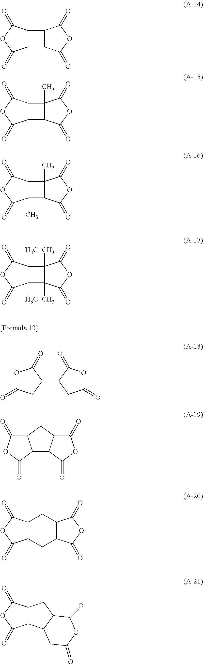


(In the formula (VIII-12), two of R1 to R10 are primary amino group, and the remainders are hydrogen atom or monovalent organic group other than primary amino group, and they are the same as or different from each other.)


A=2K 22(2πd/p−φ 2)/d·sin(φ2−φ1) (1)
- 111: power supply;
- 112: ultraviolet rays lamp;
- 113: non-polarized ultraviolet rays (whole wavelengths);
- 114: interference filter;
- 115: non-polarized ultraviolet rays (313 nm);
- 116: polarizing filter;
- 117: polarized ultraviolet rays (313 nm);
- 118: light alignment film;
- 119: glass substrate;
- 1110: heating plate;
- 100: first substrate;
- 102: TFT layer;
- 103: pixel electrode;
- 104: passivation film;
- 105: first alignment film;
- 200: second substrate;
- 201: flattened film (overcoat layer);
- 202: black matrix;
- 203: color filter;
- 204: transparent electrode;
- 205: second alignment film;
- 301: seal material;
- 302: protrusion (columnar spacer);
- 303: liquid crystal layer;
- 304: protrusion (columnar spacer);
- 401: mask pattern;
- 402: resin layer;
- L: light;
- 1, 8: polarizing plate;
- 2: first substrate;
- 3: electrode layer;
- 4: alignment film;
- 5: liquid crystal layer;
- 6: color filter;
- 203: 6G color filter green;
- 203: 6R color filter red;
- 7: second substrate;
- 11: gate electrode;
- 12: gate insulating film;
- 13: semiconductor layer;
- 14: insulating layer;
- 15: ohmic contact layer;
- 16: drain electrode;
- 17: source electrode;
- 18: insulating protective layer;
- 21: pixel electrode;
- 22: common electrode;
- 23: storage capacitor;
- 25: data wiring;
- 27: source wiring;
- 29: common line;
- 30: buffers layer.
Claims (6)


Applications Claiming Priority (3)
| Application Number | Priority Date | Filing Date | Title |
|---|---|---|---|
| JP2013-207318 | 2013-10-02 | ||
| JP2013207318 | 2013-10-02 | ||
| PCT/JP2014/076132 WO2015050132A1 (en) | 2013-10-02 | 2014-09-30 | Method for producing liquid crystal alignment film and liquid crystal display element using same |
Publications (2)
| Publication Number | Publication Date |
|---|---|
| US20160231626A1 US20160231626A1 (en) | 2016-08-11 |
| US10423033B2 true US10423033B2 (en) | 2019-09-24 |
Family
ID=52778720
Family Applications (1)
| Application Number | Title | Priority Date | Filing Date |
|---|---|---|---|
| US15/027,141 Expired - Fee Related US10423033B2 (en) | 2013-10-02 | 2014-09-30 | Method for producing liquid crystal alignment film and liquid crystal display element using same |
Country Status (5)
| Country | Link |
|---|---|
| US (1) | US10423033B2 (en) |
| JP (1) | JP5904312B2 (en) |
| CN (1) | CN105593755B (en) |
| TW (1) | TWI634373B (en) |
| WO (1) | WO2015050132A1 (en) |
Cited By (1)
| Publication number | Priority date | Publication date | Assignee | Title |
|---|---|---|---|---|
| US12448473B2 (en) | 2017-08-09 | 2025-10-21 | Rolic Technologies AG | Method for the preparation of photoaligning polymer materials and compositions |
Families Citing this family (9)
| Publication number | Priority date | Publication date | Assignee | Title |
|---|---|---|---|---|
| CN103943033B (en) * | 2014-04-02 | 2017-02-15 | 京东方科技集团股份有限公司 | Transparent display device |
| CN108137397A (en) * | 2015-09-29 | 2018-06-08 | 松下知识产权经营株式会社 | Glass panel unit, the windowpane with the glass panel unit and the method for manufacturing glass panel unit |
| TWI749019B (en) * | 2016-06-14 | 2021-12-11 | 日商日產化學工業股份有限公司 | Liquid crystal alignment agent for coating BOA substrate or substrate with BCS and liquid crystal display element |
| CN106371254A (en) * | 2016-10-28 | 2017-02-01 | 上海中航光电子有限公司 | Array substrate and display panel |
| JP2019152835A (en) * | 2018-03-06 | 2019-09-12 | シャープ株式会社 | Method for manufacturing substrate with alignment film |
| TWI683159B (en) * | 2018-11-20 | 2020-01-21 | 友達光電股份有限公司 | Display panel |
| CN113552736B (en) * | 2020-04-23 | 2024-01-30 | 中强光电股份有限公司 | Electric control visual angle switcher and display device |
| CN112375168B (en) * | 2020-10-28 | 2022-03-29 | 华南理工大学 | Side chain rod-like polar liquid crystal polymer, its preparation method and its application in nonlinear optics |
| CN115894225A (en) * | 2021-09-22 | 2023-04-04 | 晶美晟光电材料(南京)有限公司 | Preparation method of polymerizable cinnamate |
Citations (7)
| Publication number | Priority date | Publication date | Assignee | Title |
|---|---|---|---|---|
| JP2000035578A (en) | 1998-07-16 | 2000-02-02 | Tatsuo Uchida | Alignment film forming method and liquid crystal display device |
| JP2002090752A (en) | 2001-06-22 | 2002-03-27 | Matsushita Electric Ind Co Ltd | Method for manufacturing substrate with liquid crystal alignment film |
| JP2005105204A (en) | 2003-10-01 | 2005-04-21 | Jsr Corp | Method for producing liquid crystal alignment film, liquid crystal alignment film, and liquid crystal display element |
| JP2009058584A (en) | 2007-08-30 | 2009-03-19 | Jsr Corp | Liquid crystal aligning agent and method for forming liquid crystal aligning film |
| JP2009282377A (en) | 2008-05-23 | 2009-12-03 | Jsr Corp | Liquid crystal orientation agent, method for forming liquid crystal orientation film, and liquid crystal display element |
| WO2013018904A1 (en) | 2011-08-04 | 2013-02-07 | 日産化学工業株式会社 | Liquid crystal orientation liquid for light orientation processing technique, and liquid crystal orientation film employing same |
| US20160018702A1 (en) * | 2014-07-15 | 2016-01-21 | Samsung Display Co., Ltd. | Photoalignment film, method for manufacturing the same, and liquid crystal display panel including the same |
Family Cites Families (4)
| Publication number | Priority date | Publication date | Assignee | Title |
|---|---|---|---|---|
| TWI405841B (en) * | 2004-12-15 | 2013-08-21 | 大日本油墨化學工業股份有限公司 | Nematic liquid crystal composition and liquid crystal display element using same |
| WO2006078129A1 (en) * | 2005-01-20 | 2006-07-27 | Lg Chem. Ltd. | Alignment film for lcd using photoreactive polymer and lcd comprising the same |
| TWI406061B (en) * | 2005-11-10 | 2013-08-21 | Dainippon Ink & Chemicals | Composition for photoalignment film, optically anisotropic body and method of producing same |
| CN101467079B (en) * | 2006-11-08 | 2011-03-23 | Dic株式会社 | Composition for photo-alignment film, photo-alignment film, and optical isomer |
-
2014
- 2014-09-30 CN CN201480054712.XA patent/CN105593755B/en not_active Expired - Fee Related
- 2014-09-30 US US15/027,141 patent/US10423033B2/en not_active Expired - Fee Related
- 2014-09-30 WO PCT/JP2014/076132 patent/WO2015050132A1/en not_active Ceased
- 2014-09-30 JP JP2015540507A patent/JP5904312B2/en active Active
- 2014-10-01 TW TW103134177A patent/TWI634373B/en not_active IP Right Cessation
Patent Citations (7)
| Publication number | Priority date | Publication date | Assignee | Title |
|---|---|---|---|---|
| JP2000035578A (en) | 1998-07-16 | 2000-02-02 | Tatsuo Uchida | Alignment film forming method and liquid crystal display device |
| JP2002090752A (en) | 2001-06-22 | 2002-03-27 | Matsushita Electric Ind Co Ltd | Method for manufacturing substrate with liquid crystal alignment film |
| JP2005105204A (en) | 2003-10-01 | 2005-04-21 | Jsr Corp | Method for producing liquid crystal alignment film, liquid crystal alignment film, and liquid crystal display element |
| JP2009058584A (en) | 2007-08-30 | 2009-03-19 | Jsr Corp | Liquid crystal aligning agent and method for forming liquid crystal aligning film |
| JP2009282377A (en) | 2008-05-23 | 2009-12-03 | Jsr Corp | Liquid crystal orientation agent, method for forming liquid crystal orientation film, and liquid crystal display element |
| WO2013018904A1 (en) | 2011-08-04 | 2013-02-07 | 日産化学工業株式会社 | Liquid crystal orientation liquid for light orientation processing technique, and liquid crystal orientation film employing same |
| US20160018702A1 (en) * | 2014-07-15 | 2016-01-21 | Samsung Display Co., Ltd. | Photoalignment film, method for manufacturing the same, and liquid crystal display panel including the same |
Non-Patent Citations (2)
| Title |
|---|
| Hasebe et al., New Photo-Aligning Materials Having Cinnamoyl Moieties, Proceedings of the International Display Workshops (DW'14), 2014,12,02, vol. 21, pp. 44-47. |
| International Search Report dated Jan. 6, 2015, issued in counterpart Application No. PCT/JP2014/076132 (2 pages). |
Cited By (1)
| Publication number | Priority date | Publication date | Assignee | Title |
|---|---|---|---|---|
| US12448473B2 (en) | 2017-08-09 | 2025-10-21 | Rolic Technologies AG | Method for the preparation of photoaligning polymer materials and compositions |
Also Published As
| Publication number | Publication date |
|---|---|
| US20160231626A1 (en) | 2016-08-11 |
| JP5904312B2 (en) | 2016-04-13 |
| CN105593755B (en) | 2019-03-22 |
| WO2015050132A1 (en) | 2015-04-09 |
| TWI634373B (en) | 2018-09-01 |
| JPWO2015050132A1 (en) | 2017-03-09 |
| CN105593755A (en) | 2016-05-18 |
| TW201535027A (en) | 2015-09-16 |
Similar Documents
| Publication | Publication Date | Title |
|---|---|---|
| US10423033B2 (en) | Method for producing liquid crystal alignment film and liquid crystal display element using same | |
| US9695361B2 (en) | Liquid crystal composition and liquid crystal display element using the same | |
| US9683174B2 (en) | Compound, polymer, liquid crystal alignment layer, liquid crystal display device, and optically anisotropic material | |
| US10208250B2 (en) | Liquid crystal composition and liquid crystal display element using same | |
| KR102243116B1 (en) | Method of preparing a birefringent polymer film | |
| US9062247B2 (en) | Nematic liquid crystal composition and liquid crystal display element using same | |
| US9624434B2 (en) | Nematic liquid crystal composition and liquid crystal display device using the same | |
| US20160208168A1 (en) | Liquid crystal composition and liquid crystal display element using same | |
| JP6358400B2 (en) | Polymer for photo-alignment film, polymer solution, photo-alignment film, optical anisotropic body, and liquid crystal display element | |
| TWI565755B (en) | Method for the planar photoalignment | |
| JP6403030B2 (en) | Polymer for photo-alignment film, polymer solution, photo-alignment film, optical anisotropic body, and liquid crystal display element | |
| WO2017065079A1 (en) | Photo-alignment film polymer, polymer solution, photo-alignment film, optically anisotropic body, and liquid crystal display element | |
| WO2014102972A1 (en) | Fluorobiphenyl-containing composition | |
| TWI711671B (en) | Liquid crystal alignment agent, liquid crystal alignment film, liquid crystal element, liquid crystal alignment film and liquid crystal element manufacturing method | |
| JP6269832B2 (en) | Liquid crystal composition and liquid crystal display device using the same | |
| CN105462598B (en) | Liquid crystal aligning agent, liquid crystal alignment film, and liquid crystal display element | |
| US20180282625A1 (en) | Polymer, polymer solution, liquid crystal alignment layer, optically anisotropic body, and liquid crystal display element | |
| KR20200118755A (en) | Liquid crystal element and method for manufacturing same, liquid crystal composition, manufacturing methods for liquid crystal device and phase difference film, and polymer | |
| US20170260451A1 (en) | Liquid crystal composition and liquid crystal display element using the same |
Legal Events
| Date | Code | Title | Description |
|---|---|---|---|
| AS | Assignment |
Owner name: DIC CORPORATION, JAPAN Free format text: ASSIGNMENT OF ASSIGNORS INTEREST;ASSIGNORS:KODERA, FUMIAKI;KOTANI, KUNIHIKO;MARUYAMA, KAZUNORI;AND OTHERS;SIGNING DATES FROM 20160318 TO 20160323;REEL/FRAME:038186/0122 |
|
| STPP | Information on status: patent application and granting procedure in general |
Free format text: NOTICE OF ALLOWANCE MAILED -- APPLICATION RECEIVED IN OFFICE OF PUBLICATIONS |
|
| STPP | Information on status: patent application and granting procedure in general |
Free format text: PUBLICATIONS -- ISSUE FEE PAYMENT RECEIVED |
|
| STPP | Information on status: patent application and granting procedure in general |
Free format text: PUBLICATIONS -- ISSUE FEE PAYMENT VERIFIED |
|
| STCF | Information on status: patent grant |
Free format text: PATENTED CASE |
|
| FEPP | Fee payment procedure |
Free format text: MAINTENANCE FEE REMINDER MAILED (ORIGINAL EVENT CODE: REM.); ENTITY STATUS OF PATENT OWNER: LARGE ENTITY |
|
| LAPS | Lapse for failure to pay maintenance fees |
Free format text: PATENT EXPIRED FOR FAILURE TO PAY MAINTENANCE FEES (ORIGINAL EVENT CODE: EXP.); ENTITY STATUS OF PATENT OWNER: LARGE ENTITY |
|
| STCH | Information on status: patent discontinuation |
Free format text: PATENT EXPIRED DUE TO NONPAYMENT OF MAINTENANCE FEES UNDER 37 CFR 1.362 |
|
| FP | Lapsed due to failure to pay maintenance fee |
Effective date: 20230924 |