US10410570B2 - Light emitting diode display device and method for improving image quality using scheme of dividing frames into subframes - Google Patents
Light emitting diode display device and method for improving image quality using scheme of dividing frames into subframes Download PDFInfo
- Publication number
- US10410570B2 US10410570B2 US15/690,673 US201715690673A US10410570B2 US 10410570 B2 US10410570 B2 US 10410570B2 US 201715690673 A US201715690673 A US 201715690673A US 10410570 B2 US10410570 B2 US 10410570B2
- Authority
- US
- United States
- Prior art keywords
- subframes
- data
- subframe
- frame cycle
- accordance
- Prior art date
- Legal status (The legal status is an assumption and is not a legal conclusion. Google has not performed a legal analysis and makes no representation as to the accuracy of the status listed.)
- Active, expires
Links
Images


Classifications
-
- G—PHYSICS
- G09—EDUCATION; CRYPTOGRAPHY; DISPLAY; ADVERTISING; SEALS
- G09G—ARRANGEMENTS OR CIRCUITS FOR CONTROL OF INDICATING DEVICES USING STATIC MEANS TO PRESENT VARIABLE INFORMATION
- G09G3/00—Control arrangements or circuits, of interest only in connection with visual indicators other than cathode-ray tubes
- G09G3/20—Control arrangements or circuits, of interest only in connection with visual indicators other than cathode-ray tubes for presentation of an assembly of a number of characters, e.g. a page, by composing the assembly by combination of individual elements arranged in a matrix no fixed position being assigned to or needed to be assigned to the individual characters or partial characters
- G09G3/2007—Display of intermediate tones
- G09G3/2018—Display of intermediate tones by time modulation using two or more time intervals
- G09G3/2022—Display of intermediate tones by time modulation using two or more time intervals using sub-frames
- G09G3/204—Display of intermediate tones by time modulation using two or more time intervals using sub-frames the sub-frames being organized in consecutive sub-frame groups
-
- G—PHYSICS
- G09—EDUCATION; CRYPTOGRAPHY; DISPLAY; ADVERTISING; SEALS
- G09G—ARRANGEMENTS OR CIRCUITS FOR CONTROL OF INDICATING DEVICES USING STATIC MEANS TO PRESENT VARIABLE INFORMATION
- G09G3/00—Control arrangements or circuits, of interest only in connection with visual indicators other than cathode-ray tubes
- G09G3/20—Control arrangements or circuits, of interest only in connection with visual indicators other than cathode-ray tubes for presentation of an assembly of a number of characters, e.g. a page, by composing the assembly by combination of individual elements arranged in a matrix no fixed position being assigned to or needed to be assigned to the individual characters or partial characters
- G09G3/22—Control arrangements or circuits, of interest only in connection with visual indicators other than cathode-ray tubes for presentation of an assembly of a number of characters, e.g. a page, by composing the assembly by combination of individual elements arranged in a matrix no fixed position being assigned to or needed to be assigned to the individual characters or partial characters using controlled light sources
- G09G3/30—Control arrangements or circuits, of interest only in connection with visual indicators other than cathode-ray tubes for presentation of an assembly of a number of characters, e.g. a page, by composing the assembly by combination of individual elements arranged in a matrix no fixed position being assigned to or needed to be assigned to the individual characters or partial characters using controlled light sources using electroluminescent panels
- G09G3/32—Control arrangements or circuits, of interest only in connection with visual indicators other than cathode-ray tubes for presentation of an assembly of a number of characters, e.g. a page, by composing the assembly by combination of individual elements arranged in a matrix no fixed position being assigned to or needed to be assigned to the individual characters or partial characters using controlled light sources using electroluminescent panels semiconductive, e.g. using light-emitting diodes [LED]
-
- G—PHYSICS
- G09—EDUCATION; CRYPTOGRAPHY; DISPLAY; ADVERTISING; SEALS
- G09G—ARRANGEMENTS OR CIRCUITS FOR CONTROL OF INDICATING DEVICES USING STATIC MEANS TO PRESENT VARIABLE INFORMATION
- G09G2300/00—Aspects of the constitution of display devices
- G09G2300/02—Composition of display devices
- G09G2300/026—Video wall, i.e. juxtaposition of a plurality of screens to create a display screen of bigger dimensions
-
- G—PHYSICS
- G09—EDUCATION; CRYPTOGRAPHY; DISPLAY; ADVERTISING; SEALS
- G09G—ARRANGEMENTS OR CIRCUITS FOR CONTROL OF INDICATING DEVICES USING STATIC MEANS TO PRESENT VARIABLE INFORMATION
- G09G2310/00—Command of the display device
- G09G2310/02—Addressing, scanning or driving the display screen or processing steps related thereto
- G09G2310/0264—Details of driving circuits
- G09G2310/027—Details of drivers for data electrodes, the drivers handling digital grey scale data, e.g. use of D/A converters
-
- G—PHYSICS
- G09—EDUCATION; CRYPTOGRAPHY; DISPLAY; ADVERTISING; SEALS
- G09G—ARRANGEMENTS OR CIRCUITS FOR CONTROL OF INDICATING DEVICES USING STATIC MEANS TO PRESENT VARIABLE INFORMATION
- G09G2310/00—Command of the display device
- G09G2310/08—Details of timing specific for flat panels, other than clock recovery
-
- G—PHYSICS
- G09—EDUCATION; CRYPTOGRAPHY; DISPLAY; ADVERTISING; SEALS
- G09G—ARRANGEMENTS OR CIRCUITS FOR CONTROL OF INDICATING DEVICES USING STATIC MEANS TO PRESENT VARIABLE INFORMATION
- G09G2320/00—Control of display operating conditions
- G09G2320/02—Improving the quality of display appearance
- G09G2320/0233—Improving the luminance or brightness uniformity across the screen
-
- G—PHYSICS
- G09—EDUCATION; CRYPTOGRAPHY; DISPLAY; ADVERTISING; SEALS
- G09G—ARRANGEMENTS OR CIRCUITS FOR CONTROL OF INDICATING DEVICES USING STATIC MEANS TO PRESENT VARIABLE INFORMATION
- G09G2320/00—Control of display operating conditions
- G09G2320/02—Improving the quality of display appearance
- G09G2320/0242—Compensation of deficiencies in the appearance of colours
Definitions
- the present disclosure is related to the technical field of LED display screens, and in particular, to an LED display device and a method for driving the same.
- a Light-Emitting Diode (LED) display screen composed of LED display unit boards, is a modern information announcing platform. Due to the advantages of high luminous efficiency, long service life, flexible configuration, rich colors and indoor and outdoor environmental adaptability, the LED display screen has been gradually accepted by the market, in particular, the full-color LED display screen develops rapidly and has been widely used in the fields of traffic electronic identification, urban media, etc.
- LED Light-Emitting Diode
- the composition characteristic of LED display screen is modularization, that is, an LED display screen can be combined by a large number of LED display unit boards which are also known as LED display modules.
- the LED display unit boards in the same LED display screen are different in performance to some extent due to their different processes, materials and the like. So, when an image with gradually changing colors is displayed by the LED display screen assembled by the LED display unit boards, especially the LED display screen driven by Pulse Width Modulation (PWM) constant power source, the LED display unit boards displaying low overall grayscales will become comparatively dark and the LED display unit boards displaying high overall grayscales will become comparatively bright, leading to display problems. As a result, there are apparent boundary lines at the splice portion of two LED display unit boards.
- the display of grayscale is an important factor affecting the display effect of the LED display screen and is difficult to be controlled.
- the color difference between the LED display unit boards can affect the display effect of the LED display screen.
- the disclosure is to provide an LED display device and a driving method for the LED display device.
- the driving method divides each frame cycle into a plurality of subframes and adjusts the subframe display time to eliminate parasitic effects between the LED display unit boards, so as to eliminate the color differences between the LED display unit boards.
- the driving method for the LED display device includes a plurality of LED display unit boards, wherein each of the LED display unit boards is configured to display an image at a predetermined frame cycle, the frame cycle includes a plurality of subframes, each of the plurality of subframes having a respective subframe display time, the driving method includes: generating a grayscale data in accordance with an image to be displayed; generating a control signal in accordance with the grayscale data, wherein the control signal comprises a plurality of subframe signals each having a duration corresponding to a respective subframe display time; and turning on or off LED lamps arranged on each of the LED display unit boards by use of the plurality of subframe signals in each subframe of the frame cycle, wherein the frame cycle includes a reset time period between successive subframes of the plurality of subframes, and an order of the plurality of subframes in the frame cycle is adjusted in accordance with the grayscale data.
- the plurality of subframes are arranged by their subframe display times from the smallest to the largest in a predetermined order.
- the plurality of subframes arranged in the predetermined order are sequentially displayed in the frame cycle.
- the order of at least some of the plurality of subframes is adjusted randomly to form the plurality of subframes arranged in an adjusted order.
- the driving method further comprises: randomly generating an indication data in accordance with the grayscale data, wherein the indication data represents the order of at least some of the plurality of subframes.
- the grayscale data and the indication data are combined into a display data by a control terminal.
- the indication data is a binary value formed by at least one bit of the display data for indicating various adjusted orders.
- said control signal is a PWM signal.
- an LED display device comprising: a data processing module configured to generate a grayscale data in accordance with an image to be displayed; a plurality of LED display unit boards configured to the display the images at a predetermined frame cycle, the frame cycle comprises a plurality of subframes, each of the plurality of subframes having a respective subframe display time, each of the LED display unit boards comprises: a plurality of row lines and a plurality of column lines; a row driver being coupled to the plurality of row lines, and configured to provide a selecting signal; a column driver being coupled to the plurality of column lines, and configured to adjust an order of the plurality of subframes in the frame cycle in accordance with the grayscale data and generate a control signal in accordance with the grayscale data, wherein the control signal comprises a plurality of subframe signals each having a duration corresponding to a respective subframe display time; a plurality of pixel units, wherein each of the plurality of pixel units comprises an LED lamp
- the column driver is configured to arrange the plurality of subframes by their subframe display times from the smallest to the largest in a predetermined order by default.
- the column driver is configured to generate the control signal in the predetermined order in the frame cycle, when a grayscale represented by the grayscale data is equal to or smaller than the first threshold value.
- the column driver is configured to adjust the order of at least some of the plurality of subframes randomly to generate the control signal in accordance with an adjusted order, when a grayscale represented by the grayscale data is larger than the first threshold value.
- the column driver is configured to adjust the order of at least some of the plurality of subframes randomly to generate the control signal in accordance with an adjusted order, when a grayscale represented by the grayscale data is larger than the first threshold value.
- the data processing module is further configured to combine the indication data and the grayscale data into a display data, the indication data is a binary value formed by at least one bit of the display data.
- the column driver is further configured to obtain various adjusted orders in accordance with the indication data of the display data.
- said control signal is a PWM signal.
- a non-transient computer-readable storage medium on which computer instructions for performing the driving method provided according to the first aspect of the disclosure is stored.
- each frame cycle into a plurality of subframes and adjusting the subframe display time, the parasitic effect between the LED display unit boards is eliminated, such that the color difference between the LED display unit boards is eliminated.
- FIG. 1 is a flow diagram of a driving method for an LED display device according to an embodiment of the disclosure
- FIG. 2 is a schematic diagram of an LED display unit board according to an embodiment of the disclosure.
- FIG. 3 is a schematic diagram of an LED display device according to an embodiment of the disclosure.
- FIG. 4 is a timing diagram of a control signal according to an embodiment of the disclosure.
- FIG. 1 is a flow diagram of a driving method for an LED display device according to an embodiment of the disclosure.
- the LED display device includes a plurality of LED display unit boards, each of the LED display unit boards is configured to display an image at a predetermined frame cycle.
- Each frame cycle includes a plurality of subframes, each of the plurality of subframes has a respective subframe display time.
- a grayscale data is generated in accordance with an image to be displayed.
- the order of the plurality of subframes in the frame cycle is adjusted in accordance with the grayscale data, and a control signal is generated in accordance with the grayscale data, wherein the control signal includes a plurality of subframe signals each of which has a duration corresponding to a respective subframe display time.
- the control signal may be a PWM signal.
- the cumulative effective time of the control signal is consistent with the grayscale data.
- Reset time periods are included between the successive subframes of the plurality of subframes in the frame cycle, and the reset time periods separate the successive subframes from each other.
- the plurality of subframes may be arranged in a predetermined order, for example, in an increasing order of subframe display time.
- a grayscale represented by the grayscale data is equal to or smaller than a first threshold value
- the plurality of subframes arranged in the predetermined order are sequentially displayed in the frame cycle.
- the order of at least some of the plurality of subframes may be adjusted randomly to form the plurality of subframes arranged in an adjusted order.
- an indication data may also be generated in accordance with the grayscale data, and the indication data may be configured to represent the order of at least some of the plurality of subframes.
- a control terminal can be used to combine the grayscale data and the indication data into a display data.
- the indication data may be a binary value formed by at least one arbitrary bit of the display data for indicating various adjusted orders.
- the indication data may be a binary value formed by two least significant digits of the display data, and thus may be used to indicate four adjusted orders.
- the plurality of subframe signals are used to control the LED lamps to be turned on or off in each subframe of the frame cycle.
- FIG. 4 is a timing diagram of the control signal according to an embodiment of the disclosure.
- the scanning time period corresponding to the N th frame may be divided into subframe display time periods and reset time periods in time domain. As an example, it may be divided into four subframe display time periods, i.e. periods bc, de, fg and hi.
- the LED lamp corresponding to each of the pixels is turned on under the control of the plurality of subframe signals included in the control signal, each of which having a duration corresponding to a respective subframe display time.
- the periods ab, cd, df and gh are reset time periods, during which the LED lamp corresponding to each of the pixels is reset.
- the length of the periods bc, de, fg and hi can be determined in accordance with the grayscale data.
- the N th frame can be divided into four subframes, i.e. a first subframe, a second subframe, a third subframe and a fourth subframe, and the periods bc, de, fg and hi may be used for displaying the four subframes.
- An indication data representing the order of the four subframes can be generated in accordance with the grayscale data, and a control terminal may be used to combine the grayscale data and the indication data into the display data.
- the indication data can be a binary value formed by two least significant digits of the display data, by which four adjusted orders may be indicated. For example, when the two least significant digits are 00, the frame image is displayed in the order which takes the first subframe first, then the second subframe, the third subframe and the fourth subframe last; when the digits are 01, the frame image is displayed in the order which takes the fourth subframe first, then the first subframe, the second subframe and the third subframe last; when the digits are 10, the frame image is displayed in the order which takes the third subframe first, then the fourth subframe, the first subframe and the second subframe last; and when the digits are 11, the frame image is displayed in the order which takes the second subframe first, then the third subframe, the fourth subframe and the first subframe last.
- control signal in the current frame cycle is divided into subframe display time periods and reset time periods in time domain is not limited to the above example.
- the scanning time period of one frame cycle can be divided into multiple subframe display time periods in time domain, which is not limited to four periods.
- the length of one subframe display time can be equal or unequal to another.
- the number of the adjusted orders for indication is not limited to four, and it can be determined by the bit number and/or position of the binary value of the indication data. Specific adjusted orders can also be designed in more diverse ways.
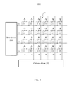
- FIG. 2 is a schematic diagram of an LED display unit board according to an embodiment of the disclosure.
- the LED display unit board 100 includes a row driver 110 , a column driver 120 and an LED matrix 130 .
- the LED matrix 130 includes a plurality of LED lamps arranged in rows and columns.
- the LED matrix 130 shown in FIG. 2 is a matrix having 4 rows*6 columns.
- Each of the plurality of LED lamps includes a cathode and an anode, and may be lightened when a forward voltage is applied between the cathode and the anode.
- the anodes of the plurality of LED lamps in one row are coupled together to a respective row line.
- the anodes of the LED lamps D 11 -D 16 in a first row are coupled together to the row line G 1 .
- the cathodes of the plurality of LED lamps in one column are coupled to a respective column line.
- the cathodes of the LED lamps D 11 -D 41 in a first column are coupled together to the column line S 1 .
- the row driver 110 is coupled to the plurality of row lines G 1 -G 4 , and provides selecting signals.
- the row driver 110 includes a plurality of selector switches, each of which is coupled to one of the plurality of row lines. When the plurality of selector switches are turned on, the corresponding row lines are coupled to the high potential terminal through the selector switches, respectively.
- a column driver 120 is coupled to the plurality of column lines S 1 to S 6 , for adjusting the order of the plurality of subframes in the frame cycle, generating a control signal in accordance with the grayscale data for each pixel, wherein the control signal includes a plurality of subframe signals each having a duration corresponding to a respective subframe display time.
- the column driver 120 arranges the plurality of subframes in a predetermined order, e.g. in an ascending order of subframe display time by default.
- the column driver 120 generates the control signal in the predetermined order in the frame cycle, when the grayscale represented by the grayscale data is equal to or smaller than the first threshold value.
- the column driver 120 adjusts the order of at least some of the subframes randomly in order to generate the control signal in the adjusted order in the frame cycle, when the grayscale represented by the grayscale data is larger than the first threshold value.
- the row driver 120 includes a plurality of constant current sources, each of which is coupled to one of the plurality of row lines.
- the row driver 110 selects a plurality of LED lamps in one row, the anodes of the selected plurality of LED lamps are coupled to a high potential, and the cathodes of the selected plurality of LED lamps are coupled to the plurality of constant current sources respectively, such that forward voltages are applied between the anodes and the cathodes of the selected plurality of LED lamps, thereby lightening the plurality of LED lamps.
- each of the plurality of LED lamps in the LED matrix 130 is used as a pixel unit. It will be understood that each pixel in the LED display device 100 may include one or more pixel units.
- each pixel in the LED display device 100 may include one or more pixel units.
- three LED lamps can be used to display the red, green, and blue color components, respectively, each of the three LED lamps produces light in corresponding color in accordance with its own light emission characteristics, or produces light in corresponding color through additional filters.
- the row driver 110 performs, for example, a progressive scan, to couple the row lines to the high voltage level sequentially. Accordingly, constant current is applied to the plurality of LED lamps in the row by the plurality of constant current sources in the column driver 120 respectively.
- the column driver 120 provides the control signal to the column lines, so that the effective lighting time of the plurality of LED lamps in the current display line is changed to display one pixel line of the image.
- the cumulative effective time of the control signal is consistent with the grayscale data
- the reset time periods are included between the successive subframes in the frame cycle, to separate the successive subframes from each other.
- the LED lamps acting as the plurality of pixel units corresponding to each of the pixels are turned on or off in accordance with the subframe signals.
- the division of a frame cycle can be performed on each row, that is, a scanning cycle of a display row line is divided into a plurality of subframe display time periods.
- FIG. 3 is a schematic diagram of an LED display device according to an embodiment of the disclosure.
- the LED display device 200 includes a plurality of LED display unit boards 100 and a data processing module 200 .
- the LED display unit board 100 has been described in detail with reference to FIG. 2 , and will not be described again.
- the number and the arrangement of the LED display unit boards 100 in the LED display device 200 are not limited to those described in FIG. 3 , which can be configured according to actual requirements.
- the data processing module 201 generates the grayscale data for each pixel in accordance with the image to be displayed.
- the plurality of LED display unit boards 100 display an image at a predetermined frame cycle, the frame cycle includes a plurality of subframes, each of the plurality of subframes has a respective subframe display time.
- the data processing module 201 generates indication data in accordance with the grayscale data and combines the indication data and the grayscale data into the display data.
- the indication data represents the order of at least some of the plurality of subframes.
- the data processing module 201 further combines the indication data in form of binary value with the grayscale data, the indication data can be implemented as a binary value formed by at least one bit of the display data for indicating various adjusted orders.
- the indication data can be formed by two least significant digits of the binary value of the display data, the data processing module 201 can instruct the column driver 120 in the LED display unit board 100 to realize four adjusted orders according to the two least significant digits of the display data.
- the column driver 120 divides a frame cycle into a plurality of subframe display time periods and a plurality of reset time periods in time domain, the reset time periods separate the successive subframes from each other.
- the column driver 120 generates the subframe signals included in the control signal during the subframe display time periods.
- the column driver 120 also uses the subframe signals to control the constant current sources to provide driving current for lighting the LED lamps.
- the control signal which is generated in accordance with the grayscale data, includes the plurality of subframe signals each having a duration corresponding to a respective subframe display time.
- the column driver 120 resets the output signal to a state before the control signal is generated, and the LED lamps are reset during the reset time periods.
- the above plurality of subframe display time may be different in length in time domain. The order of the control signal of the embodiment has been described in detail with reference to FIG. 4 , and will not repeat again.
- each frame cycle into a plurality of subframes and adjusting the subframe display time
- parasitic effects between the LED display unit boards may be eliminated, and thus the color differences between the LED display unit boards may be eliminated.
- the steps of the method or algorithm described in connection with the embodiments may be implemented by hardware, software modules executed by a processor, or a combination of the two.
- the software modules may be stored in random access memory (RAM), memory, read only memory (ROM), electrically programmable ROM, electrically erasable programmable ROM, registers, hard disks, removable disks, CD-ROMs, or other storage medium known in any form and known in the prior art.
Abstract
Description
Claims (11)
Applications Claiming Priority (3)
| Application Number | Priority Date | Filing Date | Title |
|---|---|---|---|
| CN201710225084.2 | 2017-04-07 | ||
| CN201710225084.2A CN107016955B (en) | 2017-04-07 | 2017-04-07 | LED display and its driving method |
| CN201710225084 | 2017-04-07 |
Publications (2)
| Publication Number | Publication Date |
|---|---|
| US20180293927A1 US20180293927A1 (en) | 2018-10-11 |
| US10410570B2 true US10410570B2 (en) | 2019-09-10 |
Family
ID=59445218
Family Applications (1)
| Application Number | Title | Priority Date | Filing Date |
|---|---|---|---|
| US15/690,673 Active 2037-11-28 US10410570B2 (en) | 2017-04-07 | 2017-08-30 | Light emitting diode display device and method for improving image quality using scheme of dividing frames into subframes |
Country Status (2)
| Country | Link |
|---|---|
| US (1) | US10410570B2 (en) |
| CN (2) | CN107016955B (en) |
Families Citing this family (18)
| Publication number | Priority date | Publication date | Assignee | Title |
|---|---|---|---|---|
| CN109712560A (en) * | 2019-02-20 | 2019-05-03 | 深圳市富满电子集团股份有限公司 | A kind of driving control system of LED display module |
| CN110599945B (en) * | 2019-08-06 | 2020-10-30 | 北京集创北方科技股份有限公司 | LED display device and driving method thereof |
| CN110379368B (en) * | 2019-08-30 | 2021-04-13 | 上海中航光电子有限公司 | Driving method and driving device for pulse width and voltage mixed modulation and display device |
| CN110473493B (en) * | 2019-08-30 | 2021-04-06 | 上海中航光电子有限公司 | Display panel driving method and display device |
| US11348543B2 (en) | 2020-03-26 | 2022-05-31 | Macroblock, Inc. | Scan-type display apparatus, and driving device and driving method thereof |
| CN113450719A (en) | 2020-03-26 | 2021-09-28 | 聚积科技股份有限公司 | Driving method and driving device for scanning display |
| CN113450726A (en) * | 2020-03-26 | 2021-09-28 | 聚积科技股份有限公司 | Scanning display and driving device and driving method thereof |
| CN113450724A (en) | 2020-03-26 | 2021-09-28 | 聚积科技股份有限公司 | Scanning display and driving device thereof |
| CN113450723A (en) | 2020-03-26 | 2021-09-28 | 聚积科技股份有限公司 | Scanning display and driving device and driving method thereof |
| CN113450721A (en) | 2020-03-26 | 2021-09-28 | 聚积科技股份有限公司 | Scanning display and driving device and driving method thereof |
| CN113936613B (en) * | 2020-06-29 | 2023-07-07 | 京东方科技集团股份有限公司 | Driving method and driving device of display panel, display device and storage medium |
| CN113012624B (en) * | 2020-07-31 | 2022-04-29 | 重庆康佳光电技术研究院有限公司 | LED display device and driving method thereof |
| CN111883049A (en) * | 2020-08-12 | 2020-11-03 | 北京集创北方科技股份有限公司 | Shadow eliminating potential adjusting method, line driving circuit and LED display device |
| CN114627795A (en) * | 2020-11-26 | 2022-06-14 | 深圳市奥拓电子股份有限公司 | LED display screen subframe driving control method, device and system |
| CN114627794B (en) * | 2020-11-26 | 2024-04-02 | 深圳市奥拓电子股份有限公司 | LED display system and subframe driving control method and device thereof |
| TWI767703B (en) * | 2021-05-13 | 2022-06-11 | 聚積科技股份有限公司 | Backlight driving method and backlight driving device of scanning display |
| CN115050317B (en) * | 2022-07-15 | 2023-03-21 | 惠科股份有限公司 | Data driving circuit, display module and method for outputting driving signal |
| CN117079587B (en) * | 2023-10-16 | 2024-01-09 | 长春希达电子技术有限公司 | Active Micro-LED uniformity compensation method and display device |
Citations (6)
| Publication number | Priority date | Publication date | Assignee | Title |
|---|---|---|---|---|
| US20110080173A1 (en) * | 2009-10-07 | 2011-04-07 | Kwang-Min Kim | Mother substrate of organic light emitting displays capable of sheet unit testing and method of sheet unit testing |
| US20130141469A1 (en) * | 2011-12-01 | 2013-06-06 | Chihao Xu | Active matrix organic light-emitting diode display and method for driving the same |
| US20150187252A1 (en) * | 2013-12-27 | 2015-07-02 | Samsung Display Co., Ltd. | Driving method of display apparatus and display apparatus |
| US20160189597A1 (en) * | 2014-12-24 | 2016-06-30 | Lg Display Co., Ltd. | Organic Light Emitting Display and Method of Driving the Same |
| US20170026600A1 (en) * | 2015-07-23 | 2017-01-26 | Samsung Electronics Co., Ltd. | Image sensor module and image sensor device including the same |
| CN206134209U (en) | 2016-08-24 | 2017-04-26 | 合肥集创微电子科技有限公司 | LED display screen and control circuit thereof |
Family Cites Families (9)
| Publication number | Priority date | Publication date | Assignee | Title |
|---|---|---|---|---|
| US6774876B2 (en) * | 2000-10-02 | 2004-08-10 | Semiconductor Energy Laboratory Co., Ltd. | Self light emitting device and driving method thereof |
| JP2005107063A (en) * | 2003-09-30 | 2005-04-21 | Tohoku Pioneer Corp | Device and method for driving self-luminous display panel |
| CN102801899A (en) * | 2012-08-29 | 2012-11-28 | 广东威创视讯科技股份有限公司 | Method and device for improving image display quality of spliced screen |
| KR102380763B1 (en) * | 2014-12-30 | 2022-04-01 | 엘지디스플레이 주식회사 | Organic light emitting display device and driving method thereof |
| CN105096821B (en) * | 2015-05-21 | 2017-06-09 | 杭州视芯科技有限公司 | Gray scale display drive method and gray scale display drive apparatus |
| CN105047139B (en) * | 2015-09-22 | 2018-07-13 | 深圳市华星光电技术有限公司 | The digital driving method of OLED display |
| CN105551432B (en) * | 2016-02-05 | 2018-09-04 | 赵建东 | Gray scale display drive method and gray scale display drive apparatus |
| CN105825806B (en) * | 2016-05-24 | 2018-08-07 | 北京集创北方科技股份有限公司 | LED display driving systems, control method and LED display |
| CN106251806B (en) * | 2016-09-29 | 2019-04-02 | 北京集创北方科技股份有限公司 | LED display and its driving method |
-
2017
- 2017-04-07 CN CN201710225084.2A patent/CN107016955B/en active Active
- 2017-04-07 CN CN201910495817.3A patent/CN110223628B/en active Active
- 2017-08-30 US US15/690,673 patent/US10410570B2/en active Active
Patent Citations (6)
| Publication number | Priority date | Publication date | Assignee | Title |
|---|---|---|---|---|
| US20110080173A1 (en) * | 2009-10-07 | 2011-04-07 | Kwang-Min Kim | Mother substrate of organic light emitting displays capable of sheet unit testing and method of sheet unit testing |
| US20130141469A1 (en) * | 2011-12-01 | 2013-06-06 | Chihao Xu | Active matrix organic light-emitting diode display and method for driving the same |
| US20150187252A1 (en) * | 2013-12-27 | 2015-07-02 | Samsung Display Co., Ltd. | Driving method of display apparatus and display apparatus |
| US20160189597A1 (en) * | 2014-12-24 | 2016-06-30 | Lg Display Co., Ltd. | Organic Light Emitting Display and Method of Driving the Same |
| US20170026600A1 (en) * | 2015-07-23 | 2017-01-26 | Samsung Electronics Co., Ltd. | Image sensor module and image sensor device including the same |
| CN206134209U (en) | 2016-08-24 | 2017-04-26 | 合肥集创微电子科技有限公司 | LED display screen and control circuit thereof |
Also Published As
| Publication number | Publication date |
|---|---|
| CN110223628B (en) | 2021-04-23 |
| CN110223628A (en) | 2019-09-10 |
| US20180293927A1 (en) | 2018-10-11 |
| CN107016955B (en) | 2019-08-02 |
| CN107016955A (en) | 2017-08-04 |
Similar Documents
| Publication | Publication Date | Title |
|---|---|---|
| US10410570B2 (en) | Light emitting diode display device and method for improving image quality using scheme of dividing frames into subframes | |
| US20200402450A1 (en) | Display optimization techniques for micro-led devices and arrays | |
| CN100476930C (en) | Organic light emitting display and method of driving the same | |
| US8514209B2 (en) | Display apparatus and method for driving the same | |
| EP2128687A1 (en) | Light source device and liquid crystal display device | |
| JP2009053687A (en) | Back light unit and its usage | |
| US10339851B2 (en) | Display apparatus, lighting control circuit, and method of lighting display apparatus | |
| US10347174B2 (en) | System of compressed frame scanning for a display and a method thereof | |
| JP2010250320A (en) | Method for correcting pixel data, and display apparatus for performing the method | |
| US20070211179A1 (en) | Colour display device | |
| KR20100054494A (en) | Method of driving light-source, light-source apparatus for performing the method and display apparatus having the light-source apparatus | |
| KR20180050125A (en) | LED display device, and method for operating the same | |
| CN110599948A (en) | Driving method of display device | |
| CN111341278A (en) | Overdrive processing method and overdrive device for image data | |
| CN110599945B (en) | LED display device and driving method thereof | |
| CN116386519B (en) | LED driving circuit, driving method, chip and display device | |
| US10152909B2 (en) | Display apparatus | |
| JP2006195306A (en) | Method and equipment for driving light-emitting device, and display device | |
| KR101481072B1 (en) | Image display device having variable refresh rate according to gradation bit(data), image processing method and electronic display system using the same | |
| JP2010250193A (en) | Image display device | |
| TW202226188A (en) | Gamma debugging method and gamma debugging device for display panel | |
| JP2009516223A (en) | Display method in active matrix display device | |
| CN114822342A (en) | Gamma debugging method and device for display panel | |
| US10283041B2 (en) | Display device | |
| US20170098405A1 (en) | Display device |
Legal Events
| Date | Code | Title | Description |
|---|---|---|---|
| AS | Assignment |
Owner name: CHIPONW MICROELECTRONICS TECHNOLOGY (HEFEI) CO., C Free format text: ASSIGNMENT OF ASSIGNORS INTEREST;ASSIGNORS:TANG, YONGSHENG;WANG, YONG;LIU, HAIFENG;AND OTHERS;REEL/FRAME:043447/0680 Effective date: 20170830 |
|
| FEPP | Fee payment procedure |
Free format text: ENTITY STATUS SET TO UNDISCOUNTED (ORIGINAL EVENT CODE: BIG.); ENTITY STATUS OF PATENT OWNER: SMALL ENTITY |
|
| FEPP | Fee payment procedure |
Free format text: ENTITY STATUS SET TO SMALL (ORIGINAL EVENT CODE: SMAL); ENTITY STATUS OF PATENT OWNER: SMALL ENTITY |
|
| STPP | Information on status: patent application and granting procedure in general |
Free format text: NON FINAL ACTION MAILED |
|
| STPP | Information on status: patent application and granting procedure in general |
Free format text: PUBLICATIONS -- ISSUE FEE PAYMENT RECEIVED |
|
| STPP | Information on status: patent application and granting procedure in general |
Free format text: PUBLICATIONS -- ISSUE FEE PAYMENT VERIFIED |
|
| STCF | Information on status: patent grant |
Free format text: PATENTED CASE |
|
| MAFP | Maintenance fee payment |
Free format text: PAYMENT OF MAINTENANCE FEE, 4TH YR, SMALL ENTITY (ORIGINAL EVENT CODE: M2551); ENTITY STATUS OF PATENT OWNER: SMALL ENTITY Year of fee payment: 4 |