US10401397B2 - Device for measuring integrated circuit current and method of measuring integrated circuit current using the device - Google Patents
Device for measuring integrated circuit current and method of measuring integrated circuit current using the device Download PDFInfo
- Publication number
- US10401397B2 US10401397B2 US14/174,375 US201414174375A US10401397B2 US 10401397 B2 US10401397 B2 US 10401397B2 US 201414174375 A US201414174375 A US 201414174375A US 10401397 B2 US10401397 B2 US 10401397B2
- Authority
- US
- United States
- Prior art keywords
- transfer function
- voltage
- function value
- current
- output voltage
- Prior art date
- Legal status (The legal status is an assumption and is not a legal conclusion. Google has not performed a legal analysis and makes no representation as to the accuracy of the status listed.)
- Expired - Fee Related, expires
Links
Images


Classifications
-
- G—PHYSICS
- G01—MEASURING; TESTING
- G01R—MEASURING ELECTRIC VARIABLES; MEASURING MAGNETIC VARIABLES
- G01R1/00—Details of instruments or arrangements of the types included in groups G01R5/00 - G01R13/00 and G01R31/00
- G01R1/02—General constructional details
- G01R1/06—Measuring leads; Measuring probes
- G01R1/067—Measuring probes
-
- G—PHYSICS
- G01—MEASURING; TESTING
- G01R—MEASURING ELECTRIC VARIABLES; MEASURING MAGNETIC VARIABLES
- G01R19/00—Arrangements for measuring currents or voltages or for indicating presence or sign thereof
- G01R19/0092—Arrangements for measuring currents or voltages or for indicating presence or sign thereof measuring current only
-
- G—PHYSICS
- G01—MEASURING; TESTING
- G01R—MEASURING ELECTRIC VARIABLES; MEASURING MAGNETIC VARIABLES
- G01R19/00—Arrangements for measuring currents or voltages or for indicating presence or sign thereof
- G01R19/08—Measuring current density
Definitions
- the present disclosure relates to a device and a method for measuring integrated circuit current. More particularly, the present disclosure relates to a device and a method for measuring integrated circuit current, which are used to design an efficient Power Distribution Network (PDN).
- PDN Power Distribution Network
- Integrated Circuits mounted on a Printed Circuit Board (PCB) have been developed to operate with a high power consumption at a low operating voltage and a high operating frequency.
- PCB Printed Circuit Board
- An increase of consumed current in the ICs means an occurrence of voltage noise Vnoise caused by inductance of the PDN.
- the voltage noise Vnoise may be indicated by Equation (1) below.
- V noise L ⁇ d ⁇ ⁇ I d ⁇ ⁇ t Equation ⁇ ⁇ ( 1 )
- the voltage noise V noise occurring by Equation (1) causes a stable operation error in a corresponding IC, and also propagates through the PDN so as to have a bad effect on another IC adjacent thereto. Further, the voltage noise V noise radiates outside of a device and causes an Electromagnetic Interference (EMI) problem. Therefore, a design of the PDN capable of restraining the voltage noise V noise is very important.
- EMI Electromagnetic Interference
- the method of using the SPICE model information of the IC is a method of obtaining the information on the IC current by using the SPICE model information of the IC. That is, if the SPICE model information of the IC is secured, the IC current information may be obtained by using a Chip Power Model (CPM) of a sentinel simulation tool. Accordingly, the IC current information may be extracted in a frequency range from a DC band to a several GHz band, and a system simulation in which all the IC, a package including the IC and a PCB including the IC and the package are considered, may be performed by using the IC current information.
- CPM Chip Power Model
- the method of measuring the IC current at a position of designing the bulk and de-coupling capacitor is a method of obtaining the IC current by using a magnetic loop probe. That is, the current value measured at a position of the de-coupling capacitor and the bulk capacitor by using the magnetic loop probe is regarded as the IC current.
- the IC current includes various current components, and each current component includes different frequency components. Accordingly, the IC current is established by a combination of the different frequency values.
- FIG. 1 is a graph illustrating a frequency distribution of an IC current according to the related art.
- a capacitor supplying an IC with electric current depending on a frequency range is determined by each Self Resonance Frequency (SRF). That is, the IC current corresponding to a frequency range (i ODC region) of more than several hundred MHz is an electric current (i ODC ) supplied by On-Die Capacitance (ODC) present in the IC, and the IC current corresponding to a frequency range (i decap region) of several MHz to several hundred MHz is an electric current (i decap ) supplied by the de-coupling capacitor.
- SRF Self Resonance Frequency
- the IC current corresponding to a frequency range (i bulk region) corresponding to a frequency range equal to or less than several MHz is an electric current (i bulk ) supplied by the bulk capacitor and a Voltage Regulation Module (VRM). Accordingly, the electric current measured on the de-coupling capacitor and the bulk capacitor corresponds to an electric current in a corresponding frequency range of the IC.
- VRM Voltage Regulation Module
- the method of inserting the current probe in the IC is a method of measuring the IC current by using the magnetic coupling scheme in which the current probe is inserted in the IC. If this method is used, the current component supplied by the ODC may be extracted. In comparison with the simplified current measurement model of the previous methods (1) and (2), this method has an advantage of providing very precise information. However, since the current probe is always inserted in the IC to be measured in order to use the method (3), there is a disadvantage in view of efficiency of a space and a cost.
- a method of extracting an IC current which is capable of obtaining IC current information in various operating circumstances and environments and extracting a component of the IC current supplied by On-Die Capacitance (ODC) is desired.
- ODC On-Die Capacitance
- an aspect of the present disclosure is to provide a method of extracting an IC current, which is capable of obtaining IC current information in various operating circumstances and environments and extracting a component of the IC current supplied by On-Die Capacitance (ODC).
- ODC On-Die Capacitance
- Another aspect of the present disclosure is to provide a device for extracting an IC current, which is capable of obtaining IC current information in various operating circumstances and environments and extracting a component of the IC current supplied by On-Die Capacitance (ODC).
- ODC On-Die Capacitance
- a method of extracting an Integrated Circuit (IC) current using an IC current extracting device the IC current extracting device electrically connected to a substrate provided with an IC is provided.
- the method includes generating a transfer function value by using a measurement voltage measured in a node nearest an input terminal of the IC, substituting the generated transfer function value for a reverse fast Fourier transform function so as to extract the IC voltage, and extracting the IC current by simulating the extracted IC voltage in a time domain.
- a device for extracting an Integrated Circuit (IC) current the device provided on a substrate.
- the device includes a transfer function generating unit configured to generate a transfer function value using a voltage of a node nearest an input terminal of the IC, an IC voltage extracting unit configured to convert the generated transfer function value into a reverse fast Fourier transform to extract the IC voltage, and an IC current extracting unit configured to extract the IC current by simulating the extracted IC voltage in a time domain.
- FIG. 1 is a graph illustrating a frequency distribution of an Integrated Circuit (IC) current according to the related art
- FIG. 2 is a view illustrating a configuration of a system according to an embodiment of the present disclosure
- FIG. 3 is a block diagram schematically illustrating an internal structure of an IC current meter shown in FIG. 2 according to an embodiment of the present disclosure
- FIG. 4 is a flowchart illustrating a process of extracting an IC current using an IC current meter shown in FIG. 2 according to an embodiment of the present disclosure
- FIG. 5 is a circuit diagram illustrating an equivalent circuit of a Power Distribution Network (PDN) model applied to the system shown in FIG. 1 according to an embodiment of the present disclosure
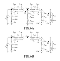
- FIGS. 6A and 6B is circuit diagrams illustrating the equivalent circuit of the PDN model shown in FIG. 5 , in which negligible parameters, i.e., Cpkg and Cpcb are removed and electric current flow is shown according to a presence or an absence of a de-coupling capacitor according to an embodiment of the present disclosure;
- FIG. 7 is a view illustrating a transfer function based on an S-parameter according to an embodiment of the present disclosure
- FIG. 8 is a view illustrating a transfer function based on a time domain according to an embodiment of the present disclosure
- FIGS. 9A, 9B, 9C, and 9D are graphs illustrating a reason of excessively calculating an IC voltage in the case where a probe noise is not considered according to an embodiment of the present disclosure
- FIG. 10 is a view illustrating a simulation in a time domain for extracting an IC current according to an embodiment of the present disclosure
- FIG. 11 is a view illustrating a simulation in a time domain for optimizing the de-coupling capacitor according to an embodiment of the present disclosure
- FIG. 12 is a view illustrating a core circuit of 1.2V in which a Voltage Regulation Module (VRM), a PDN, an IC (package and die) and nine de-coupling capacitors are arranged according to an embodiment of the present disclosure;
- VRM Voltage Regulation Module
- FIG. 13 is a graph illustrating PDN impedance of FIG. 12 according to an embodiment of the present disclosure.
- FIG. 14 is a graph illustrating a comparison of a result of a time domain simulation based on a transfer function with a result of a simulation based on a new transfer function proposed in the present disclosure, in a case where a noise level of an oscilloscope probe is 0.05 mV according to an embodiment of the present disclosure;
- FIG. 15 is a view illustrating waveforms in a time domain of a extracted IC current according to an embodiment of the present disclosure
- FIG. 16A is a graph illustrating a comparative result when a nine de-coupling capacitors are removed according to an embodiment of the present disclosure
- FIG. 16B is a graph illustrating a comparative result when no de-coupling capacitor is removed according to an embodiment of the present disclosure
- FIG. 17 is a graph illustrating a comparison of a predicted Vpp percentage with a measured Vpp percentage with relation to a number of de-coupling capacitors according to an embodiment of the present disclosure.
- IC Integrated Circuit
- PDN Power Distribution Network
- FIG. 2 is a view illustrating a configuration of a system according to an embodiment of the present disclosure.
- a system 300 in order to obtain the accurate IC current information, includes a board 110 which is provided with a corresponding IC of which a designer wants to obtain an IC current, and an IC current meter 200 for measuring a voltage at a measurement point (or node) on the board in order to obtain the IC current of the IC.
- the board 110 is provided with a voltage regulation module (VRM) 112 for providing the IC with a constant voltage, an IC 114 for receiving an input of a voltage from the VRM 112 so as to operate, and a power trace 116 for electrically connecting the VRM 112 with the IC 114 .
- VRM voltage regulation module
- the power trace 116 has a structure in that a plurality of capacitors such as a bulk capacitor for filtering a voltage noise C 1 and a de-coupling capacitor C 2 are parallel connected.
- the IC current meter 200 receives an input of a voltage V decap which is measured at a certain measurement point on the board 110 so as to calculate (extract or calculate) the accurate IC current, in which the measured V voltage V decap is a voltage V decap which is measured at a measurement point nearest a voltage input terminal of the IC 114 , and the measurement point is a measurement point of the de-coupling capacitor C 2 nearest the voltage input terminal of the IC.
- the V voltage V decap which is measured at the measurement point is a voltage which is measured in the state that the de-coupling capacitor C 2 is removed. This will be described in detail below.
- the IC current meter 200 receives an input of the measured voltage V decap through a probe head 212 mounted at a Measurement Point (MP) and a probe cable 214 , so as to extract the accurate IC current value.
- MP Measurement Point
- FIG. 3 is a block diagram schematically illustrating an internal structure of an IC current meter shown in FIG. 2 according to an embodiment of the present disclosure.
- the IC current meter 200 includes an input unit 210 , a transfer function generating unit 220 , an IC voltage extraction unit 230 and an IC current extraction unit 240 .
- the input unit 210 receives an input of a voltage V decap which is measured at a point of the de-coupling capacitor C 2 nearest an input terminal of the IC 114 among the de-coupling capacitors which are removed from the board 110 , and includes the probe having the probe head 212 and the probe cable 214 shown in FIG. 2 .
- the transfer function generating unit 220 receives the measured voltage V decap through the input unit 210 , and generates the transfer function by using the voltage V decap .
- the transfer generating unit 220 generates a new transfer function, V New-TF, to which a probe noise level is applied in order to compensate for the probe noise generated at the measurement point in the measuring process. This will be described in detail below.
- the IC voltage extraction unit 230 receives a transfer function through the transfer function unit 220 and extracts the IC voltage by using the transfer function, and extracts the IC voltage by substituting the transfer function for a reverse fast Fourier transform function so as to extract the IC voltage.
- the IC current extraction unit 240 receives the IC voltage extracted by the IC voltage extraction unit 230 , and obtains the IC current through a simulation at a time domain.
- FIG. 4 is a flowchart illustrating a process of extracting an IC current using an IC current meter shown in FIG. 2 according to an embodiment of the present disclosure.
- operation S 401 after the capacitors on the board are removed, a process of measuring a voltage (a measured voltage on a board) at a position (or node) of the de-coupling capacitor nearest the IC is performed.
- On-Die Capacitance/On-Die Resistance of the IC is measured.
- a two-port shunt-thru process is used to measure low impedance, and the low impedance may be measured by a network analyzer.
- the process of measuring the ODC/ODR of the IC is described in below documents [1] and [2]. Accordingly, the detailed description of the process will be omitted.
- a transfer function is generated by using a board measuring voltage, the ODC/ODR of the IC and the S-parameter which are obtained respectively in operations S 401 , S 403 and S 405 , and a process of extracting the IC voltage by using the generated transfer function is performed.
- operation S 411 the voltage of the corresponding board is extracted (predicted) by using the extracted IC current, and in operation S 415 , a design of the PDN of the corresponding board is optimized.
- operation S 413 the voltage of another board is extracted (predicted) by using the extracted IC current similarly to operation S 413 , and in operation S 417 , a design of the PDN of the board is optimized based on the voltage ripple.
- FIG. 5 is a circuit diagram illustrating an equivalent circuit of a PDN model applied to the system shown in FIG. 2 according to an embodiment of the present disclosure.
- the S-parameter of the board and the package may be obtained, and manual parts of an ODC, an ODR, an Rvrm and an Lvram may be determined by the shunt-thru method of operation S 403 . Accordingly, a single unknown parameter of FIG. 5 is an IC current extracted by the proposed method of the present disclosure.
- the voltage measurement should to be performed when the IC is in the worst operation state in order to obtain the worst IC current.
- the measurement is performed at a point of a de-coupling capacitor nearest the IC after the capacitor is removed. As a distance between a measurement point (MP of FIGS. 2 and 5 ) and the IC is gradually shorter, the inductance of the board becomes low. By removing the de-coupling capacitor from the measurement point (MP of FIGS. 2 and 5 ), a voltage waveform similar to the IC voltage waveform may be obtained.
- FIGS. 6A and 6B are circuit diagrams illustrating the equivalent circuit of the PDN model shown in FIG. 5 , in which negligible parameters, i.e., Cpkg and Cpcb are removed and electric current flow is shown according to a presence or an absence of a de-coupling capacitor according to an embodiment of the present disclosure.
- FIG. 6A a circuit diagram illustrating an equivalent circuit in the case that the de-coupling capacitor is present
- FIG. 6B a circuit diagram illustrating an equivalent circuit in the case that the de-coupling capacitor is removed.
- electric current i 1 of Zdie and electric current i 2 of Zpkg may be expressed by Equation (2) below.
- i 1 Z pkg + ⁇ Z decap
- Z vrm ) ] ⁇ ⁇ i die ⁇ ⁇ i 2 Z die Z die + Z pkg + ⁇ Z decap
- electric current i′ 1 of Zdie and electric current i′ 2 may be expressed by Equation (3) below.
- i 1 ′ Z pkg + Z pcb + ( Z bulk
- Z vrm ) ⁇ i die ⁇ ⁇ i 2 ′ Z die Z die + Z pkg + Z pcb + ( Z bulk
- FIG. 7 is a view illustrating a transfer function based on an S-parameter according to an embodiment of the present disclosure.
- an S-parameter input-to-output transfer function (STF) may be expressed by Equation (4) below.
- FIG. 8 is a view illustrating a transfer function based on a time domain according to an embodiment of the present disclosure.
- TTF time domain transfer function
- V die of operation S 407 of FIG. 4 may be calculated by Equation (6) below.
- v die IFFT ⁇ FFT [ v in ( t )]/( STF or TTF ) ⁇ Equation (6)
- FIGS. 9A, 9B, 9C and 9D are graphs illustrating a reason of excessively calculating an IC voltage in a case where a probe noise is not considered according to an embodiment of the present disclosure.
- a high-frequency component may be excessively compensated when the IC voltage is extracted by using the TTF value. Further, in a certain frequency, a portion exists in which the Vout(f) becomes very large in comparison with the Vin(f) because of a series resonance due to the S-parameter of the ODC/ODR, the board and the package of the IC.
- a new transfer function NEWTF is proposed like Table 1 below in order to remove the probe noise.
- V in (f) FET[V in (t)]
- V out (f) FET[V out (t)]
- PNL is a probe noise level
- the transfer function is defined as 1, while if the values of the Vin(f) and the Vout(f) are larger than the probe noise level, the TTF is applied.
- the STF and TTF may be used.
- the IC voltage may be calculated by using the transfer function (STF, TTF or NEWTF) obtained in such a manner as described above according to Equation (7) below.
- the below Equation (7) is to calculate an IC voltage according to a new transfer function. Accordingly, the calculation of the IC voltage using the STF or TTF may be performed by substituting the STF or TTF for the NEWTF used as the denominator in Equation (7).
- v die IFFT ⁇ FFT [ v in ( t )]/ NEWTF ⁇ Equation (7)
- FIG. 10 is a view illustrating a simulation in a time domain for extracting the IC current according to an embodiment of the present disclosure.
- the optimization of the de-coupling capacitor may be performed according to the voltage noise level through the simulation as shown in FIG. 11 .
- FIG. 11 is a view illustrating a simulation in a time domain for optimizing a de-coupling capacitor according to an embodiment of the present disclosure.
- FIG. 12 is a view illustrating a core circuit of 1.2V in which a VRM, a PDN, an IC (package and die) and nine de-coupling capacitors are arranged according to an embodiment of the present disclosure.
- the VRM 1201 , PDN 1203 and IC (package and die) 1205 are arranged on top and inner layers and the nine capacitors are arranged on a bottom layer 1209 , in the prepared core circuit of 1.2V.
- One de-coupling capacitor among the nine de-coupling capacitors, which is located nearest an input terminal of the IC, is set as a measurement point 1211 as shown in the drawing.
- the IC current of the core circuit of 1.2V was extracted and the measured information was compared with simulated current information at a measurement point of the de-coupling capacitor.
- the detailed result is as follows.
- a PDN impedance including a VRM model and an IC model were measured at a measurement point 1211 through a shunt-thru method by using the network analyzer.
- the network analyzer may be, for example, Agilent E5061B.
- the manual parts (ODC, ODR, Rvrm and Lvrm) shown in FIG. 5 may be calculated by a curve-fitting method.
- FIG. 13 is a graph illustrating a calculation result of a PDN impedance of FIG. 12 according to an embodiment of the present disclosure.
- the voltage waveform of the board was measured by using a digital oscilloscope (Tektronix DSA70404C) at the identical point under the worst condition.
- the IC voltage data was determined by Equation (7).
- FIG. 14 is a graph illustrating a comparison of a result of a time domain simulation based on a transfer function (TTF) with a result of a simulation based on a new transfer function (NEW-TF) proposed in the present disclosure, in the case that a noise level of an oscilloscope probe is 0.05 mV according to an embodiment of the present disclosure.
- TTF transfer function
- NAW-TF new transfer function
- the probe noise level is remarkably reduced by the new transfer function (NEW-TF) proposed in the present disclosure.
- the IC current is calculated through the time domain simulation shown in FIGS. 9C and 9D .
- the time domain waveform of the extracted IC current is shown in FIG. 15 .
- FIG. 15 is a view illustrating waveforms in the time domain of an extracted IC current according to an embodiment of the present disclosure.
- FIG. 15 waveforms in the time domain of the extracted IC current according to an embodiment are illustrated.
- the simulated voltage data and the measured data are compared by using the extracted IC current as a source of FIG. 10 in the frequency domain.
- FIG. 16A is a graph illustrating a comparative result when a nine de-coupling capacitors are removed according to an embodiment of the present disclosure
- FIG. 16B is a graph illustrating a comparative result when no de-coupling capacitors are removed according to an embodiment of the present disclosure.
- a below Table 2 indicates a comparison of a voltage peak to peak data Vpp according to the number of the decoupling capacitors.
- a predicted (simulated) Vpp and a measured Vpp are decreased when the number of the de-coupling capacitors increases, and a result preferably corresponds to an error less than 10 mV.
- Table 2 indicates a comparison of magnitude of a voltage ripple with a simulated magnitude instead of the time domain waveform because of a difficulty in measuring data in the identical time.
- FIG. 17 is a graph illustrating a comparison of a predicted Vpp percentage with a measured Vpp percentage with relation to a number of de-coupling capacitors.
- a difference between the predicted Vpp percentage and the measured Vpp percentage is less than 1%. The result is sufficient to verify the method of extracting the proposed accurate IC current.
- a new input-to-output transfer function to which the probe noise effect is applied is proposed, and it is known that the accurate IC voltage may be obtained by the proposed new transfer function.
- the accurate IC current is finally extracted by using the IC voltage waveform and the PDN information.
- the proposed method is verified by comparing the simulated voltage information using the extracted IC current as the source with the measured voltage information.
- the IC extracting method proposed by the present disclosure may be usefully used in the design and optimization of the PDN.
- the voltage of the corresponding board is predicted by using the extracted IC current so that the design of the PDN on the corresponding board may be optimized based on the voltage ripple.
- the voltage of another board using an identical IC is predicted by using the extracted IC current so that the design of the PDN on the corresponding board may be optimized based on the voltage ripple.
Abstract
Description
functions are a source of the voltage noise Vnoise.
- [1] L. D. Smith, S. Sun, M. Sarmiento, Z. Li and K. Chandrasekar, “On-Die Capacitance Measurements in the Frequency and Time Domains,” Presented at the DesignCon 2011, Santa Clara, Calif.
- [2] Application note, “Evaluating DC-DC Converters and PDN with the E5061B LF-RF Network Analyzer,” Agilent Technologies, Inc., September 2012.
-
- Measurement of the voltage on the board in operation S401 of
FIG. 4
- Measurement of the voltage on the board in operation S401 of
-
- Extraction of IC voltage and IC current in operations S407 and S409 of
FIG. 4 .
- Extraction of IC voltage and IC current in operations S407 and S409 of
TTF=FFT[v out(t)]/FFT[v in(t)] Equation (5)
v die =IFFT{FFT[v in(t)]/(STF or TTF)} Equation (6)
| TABLE 1 | ||||
| |
|
|||
| Vin(f) > Vout(f) | Vin(f) > PNL | Vout(f)/Vin(f) | ||
| Vin(f) ≤ |
1 | |||
| Vin(f) ≤ Vout(f) | Vout(f) > PNL | Vout(f)/Vin(f) | ||
| Vout(f) ≤ |
1 | |||
v die =IFFT{FFT[v in(t)]/NEWTF} Equation (7)
| TABLE 2 | ||||||
| Number | ||||||
| of | ||||||
| 100 nF | Predicted | Measured | Predicted | Measured | ΔVpp | ΔVpp |
| Decpa | Vpp (mV) | Vpp (mV) | Vpp (%) | Vpp (%) | (mV) | ( %) |
| 0 | 165 | 162 | 13.8 | 13.5 | 3 | 0.3 |
| 1 | 79 | 80 | 6.6 | 6.7 | −1 | −0.1 |
| 2 | 60 | 66 | 5.0 | 5.5 | −6 | −0.5 |
| 3 | 52 | 54 | 4.3 | 4.5 | −2 | −0.2 |
| 4 | 48 | 56 | 4.0 | 4.7 | −8 | −0.7 |
| 5 | 44 | 52 | 3.7 | 4.3 | −8 | −0.6 |
| 6 | 41 | 52 | 3.4 | 4.3 | −11 | −0.9 |
| 7 | 39 | 44 | 3.3 | 3.7 | −5 | −0.4 |
| 8 | 37 | 46 | 3.1 | 3.8 | −9 | −0.7 |
| 9 | 35 | 42 | 2.9 | 3.5 | −7 | −0.6 |
Claims (20)
Applications Claiming Priority (2)
| Application Number | Priority Date | Filing Date | Title |
|---|---|---|---|
| KR10-2013-0013673 | 2013-02-07 | ||
| KR1020130013673A KR102028921B1 (en) | 2013-02-07 | 2013-02-07 | Device for measuring integrated circuit current and method for measuring integrated circuit current using the device |
Publications (2)
| Publication Number | Publication Date |
|---|---|
| US20140222360A1 US20140222360A1 (en) | 2014-08-07 |
| US10401397B2 true US10401397B2 (en) | 2019-09-03 |
Family
ID=51259979
Family Applications (1)
| Application Number | Title | Priority Date | Filing Date |
|---|---|---|---|
| US14/174,375 Expired - Fee Related US10401397B2 (en) | 2013-02-07 | 2014-02-06 | Device for measuring integrated circuit current and method of measuring integrated circuit current using the device |
Country Status (2)
| Country | Link |
|---|---|
| US (1) | US10401397B2 (en) |
| KR (1) | KR102028921B1 (en) |
Families Citing this family (4)
| Publication number | Priority date | Publication date | Assignee | Title |
|---|---|---|---|---|
| CN105306636B (en) * | 2015-10-30 | 2020-09-29 | 南京鼎臻自动化科技有限公司 | Method, circuit and system for improving power supply noise |
| US10691190B2 (en) | 2017-06-26 | 2020-06-23 | Seagate Technology Llc | Power delivery network analysis of memory unit I/O power domain |
| CN107992139B (en) * | 2017-11-22 | 2020-09-18 | 北京电子工程总体研究所 | Port excitation conversion method from time domain current source to time domain voltage source |
| KR102236526B1 (en) * | 2017-11-28 | 2021-04-05 | 에스케이하이닉스 주식회사 | Method of extracting capacitance of high frequency range using time-domain reflectometry measurement, device, and computer readable storage medium implementing thereof |
Citations (9)
| Publication number | Priority date | Publication date | Assignee | Title |
|---|---|---|---|---|
| KR950009991A (en) | 1993-09-17 | 1995-04-26 | 문정환 | On-chip peak current measurement method |
| JP2000321321A (en) | 1999-05-12 | 2000-11-24 | Hitachi Ltd | Electric constant measuring method for integrated circuit and measuring system thereof |
| JP2002197137A (en) | 2001-10-26 | 2002-07-12 | Nec Corp | Method and device for evaluating characteristic of printed circuit board, and storing medium |
| JP2004085477A (en) | 2002-08-28 | 2004-03-18 | Nec Corp | Device and method evaluating noise immunity |
| JP2009503668A (en) | 2005-07-28 | 2009-01-29 | カップリング ウェーブ ソリューションズ シーダブリュエス | Method and apparatus for supporting integrated circuit design |
| US20090058558A1 (en) * | 2006-03-01 | 2009-03-05 | Takashi Okano | Device and Connecting Method |
| US20090213558A1 (en) * | 2008-02-21 | 2009-08-27 | Hideki Osaka | Support method and apparatus for printed circuit board |
| US20120136598A1 (en) * | 2010-08-04 | 2012-05-31 | Vladimir Dmitriev-Zdorov | Optimization of Decoupling Device Choice for Electronic Design |
| US8412497B1 (en) * | 2010-09-07 | 2013-04-02 | Xilinx, Inc. | Predicting simultaneous switching output noise of an integrated circuit |
-
2013
- 2013-02-07 KR KR1020130013673A patent/KR102028921B1/en active IP Right Grant
-
2014
- 2014-02-06 US US14/174,375 patent/US10401397B2/en not_active Expired - Fee Related
Patent Citations (10)
| Publication number | Priority date | Publication date | Assignee | Title |
|---|---|---|---|---|
| KR950009991A (en) | 1993-09-17 | 1995-04-26 | 문정환 | On-chip peak current measurement method |
| JP2000321321A (en) | 1999-05-12 | 2000-11-24 | Hitachi Ltd | Electric constant measuring method for integrated circuit and measuring system thereof |
| JP2002197137A (en) | 2001-10-26 | 2002-07-12 | Nec Corp | Method and device for evaluating characteristic of printed circuit board, and storing medium |
| JP2004085477A (en) | 2002-08-28 | 2004-03-18 | Nec Corp | Device and method evaluating noise immunity |
| JP2009503668A (en) | 2005-07-28 | 2009-01-29 | カップリング ウェーブ ソリューションズ シーダブリュエス | Method and apparatus for supporting integrated circuit design |
| US20090234630A1 (en) | 2005-07-28 | 2009-09-17 | Francois Clement | Method and Apparatus for Assisting Integrated Circuit Designing |
| US20090058558A1 (en) * | 2006-03-01 | 2009-03-05 | Takashi Okano | Device and Connecting Method |
| US20090213558A1 (en) * | 2008-02-21 | 2009-08-27 | Hideki Osaka | Support method and apparatus for printed circuit board |
| US20120136598A1 (en) * | 2010-08-04 | 2012-05-31 | Vladimir Dmitriev-Zdorov | Optimization of Decoupling Device Choice for Electronic Design |
| US8412497B1 (en) * | 2010-09-07 | 2013-04-02 | Xilinx, Inc. | Predicting simultaneous switching output noise of an integrated circuit |
Non-Patent Citations (10)
| Title |
|---|
| Archambeault "Effective Power/Ground Plane Decoupling for PCB" pp. 1-104; Oct. 2007. * |
| Changhyun Cho et al., Design and Implementation of On-chip Embedded Current Probe Using Magnetic Field Coupling in Chip to Chip Wireless Power Transfer System, May 10, 2012, Terahertz Interconnection and Package Lab., Department of Electrical Engineering, KAIST 373-1 Guseong-dong, Yuseong-gu, Daejeon 305-701, South Korea, E-mail: mydearcho@kaist.ac.kr. |
| Fan Zhou et al., Measuring IC Switching Current Waveforms Using a GMI Probe for Power Integrity Studies, 2010 Asia-Pacific International Symposium on Electromagnetic Compatibility, Apr. 12-16, 2010, Beijing, China. |
| http://www.apache-da.com/products/sentinel/chip-power-model. |
| Jingook Kim et al., Closed-Form Expressions for the Maximum Transient Noise Voltage Caused by an IC Switching Current on a Power Distribution Network, IEEE Transactions on Electromagnetic Compatibility, Oct. 2012. |
| Korean Decision of Grant dated Jul. 10, 2019, issued in Korean Patent Application No. 10-2013-0013673. |
| Larry D Smith et al., On-Die Capacitance Measurements in the Frequency and Time Domains, DesignCon, Jan. 2011. |
| Liang Li et al., Measurement of multiple switching current components through a bulk decoupling capacitor using a lab-made low-cost current probe, Aug. 14, 2011, EMC Laboratory, Missouri University of Science and Technology, 4000 Enterprise Dr., Rolla, MO, 65401, USA Sony Corporation Gotenyama Tec. May 1, 2012 Kitashinagawa Shinagawa-ku, Tokyo, 141-0001, Japan. |
| Popovich "High Performance Power Distribution Networks with On-Chip Decoupling Capacitors for Nanoscale Integrated Circuits" (Year: 2007). * |
| Ultra Low impedance measurements using 2-port measurements, Agilent Technologies, Feb. 15, 2007. |
Also Published As
| Publication number | Publication date |
|---|---|
| US20140222360A1 (en) | 2014-08-07 |
| KR20140100680A (en) | 2014-08-18 |
| KR102028921B1 (en) | 2019-10-08 |
Similar Documents
| Publication | Publication Date | Title |
|---|---|---|
| Kim et al. | Improved target impedance and IC transient current measurement for power distribution network design | |
| US10401397B2 (en) | Device for measuring integrated circuit current and method of measuring integrated circuit current using the device | |
| Kim et al. | Closed-form expressions for the maximum transient noise voltage caused by an IC switching current on a power distribution network | |
| Das et al. | Modeling and characterization of the system-level Power Delivery Network for a dual-core ARM Cortex-A57 cluster in 28nm CMOS | |
| CN108959779B (en) | Decoupling network design method based on power supply noise time domain analysis | |
| Novak et al. | Frequency-domain characterization of power distribution networks | |
| Levant et al. | EMC assessment at chip and PCB level: Use of the ICEM model for jitter analysis in an integrated PLL | |
| US20150331989A1 (en) | Metal interconnect modeling | |
| US7949975B2 (en) | Apparatus and method of extracting equivalent circuit of T-type transmission circuit | |
| Murugan et al. | Multiscale EMC Modeling, Simulation, and Validation of a Synchronous Step-Down DC-DC Converter | |
| Boyer et al. | Modeling methodology of the conducted emission of a DC-DC converter board | |
| Berbel et al. | Characterization and modeling of the conducted emission of integrated circuits up to 3 GHz | |
| Maloney | HBM tester waveforms, equivalent circuits, and socket capacitance | |
| Goral et al. | Power delivery network simulation methodology including integrated circuit behavior | |
| Ben Dhia et al. | IC immunity modeling process validation using on-chip measurements | |
| Deobarro et al. | On-chip sampling and EMC modeling of I/Os switching to evaluate conducted RF disturbances propagation | |
| Song et al. | Optimal power distribution network design for high-performance solid-state-drive based on novel target-impedance extraction method | |
| Huang et al. | Analysis and modeling of passive device degradation for a long-term electromagnetic emission study of a DC–DC converter | |
| Ichikawa et al. | Experimental verification of power supply noise modeling for EMI analysis through on-board and on-chip noise measurements | |
| Dannan et al. | Improved Methodology to Accurately Perform System Level Power Integrity Analysis Including an ASIC die | |
| Erdin et al. | Pin-capacitor spacing as a design guide to power delivery networks | |
| Li et al. | Development and validation of a microcontroller model for EMC | |
| Weßling et al. | Prediction of conducted emissions produced by a DC-DC-converter using component parasitics and partial inductances | |
| Berge et al. | Analog Power Filtering: Modeling, Measuring & Analog PI | |
| Xu | System level power integrity transient analysis using a physics-based approach |
Legal Events
| Date | Code | Title | Description |
|---|---|---|---|
| AS | Assignment |
Owner name: SAMSUNG ELECTRONICS CO., LTD., KOREA, REPUBLIC OF Free format text: ASSIGNMENT OF ASSIGNORS INTEREST;ASSIGNORS:LIM, SANG-HO;LEE, SANG-HO;KO, CHEA-OK;AND OTHERS;REEL/FRAME:032161/0519 Effective date: 20140205 |
|
| STPP | Information on status: patent application and granting procedure in general |
Free format text: RESPONSE TO NON-FINAL OFFICE ACTION ENTERED AND FORWARDED TO EXAMINER |
|
| STPP | Information on status: patent application and granting procedure in general |
Free format text: NOTICE OF ALLOWANCE MAILED -- APPLICATION RECEIVED IN OFFICE OF PUBLICATIONS |
|
| STPP | Information on status: patent application and granting procedure in general |
Free format text: PUBLICATIONS -- ISSUE FEE PAYMENT VERIFIED |
|
| STPP | Information on status: patent application and granting procedure in general |
Free format text: PUBLICATIONS -- ISSUE FEE PAYMENT VERIFIED |
|
| STCF | Information on status: patent grant |
Free format text: PATENTED CASE |
|
| FEPP | Fee payment procedure |
Free format text: MAINTENANCE FEE REMINDER MAILED (ORIGINAL EVENT CODE: REM.); ENTITY STATUS OF PATENT OWNER: LARGE ENTITY |
|
| LAPS | Lapse for failure to pay maintenance fees |
Free format text: PATENT EXPIRED FOR FAILURE TO PAY MAINTENANCE FEES (ORIGINAL EVENT CODE: EXP.); ENTITY STATUS OF PATENT OWNER: LARGE ENTITY |
|
| STCH | Information on status: patent discontinuation |
Free format text: PATENT EXPIRED DUE TO NONPAYMENT OF MAINTENANCE FEES UNDER 37 CFR 1.362 |
|
| FP | Lapsed due to failure to pay maintenance fee |
Effective date: 20230903 |