US10396206B2 - Gate cut method - Google Patents
Gate cut method Download PDFInfo
- Publication number
- US10396206B2 US10396206B2 US15/643,940 US201715643940A US10396206B2 US 10396206 B2 US10396206 B2 US 10396206B2 US 201715643940 A US201715643940 A US 201715643940A US 10396206 B2 US10396206 B2 US 10396206B2
- Authority
- US
- United States
- Prior art keywords
- sacrificial gate
- gate
- oxide layer
- opening
- interlayer dielectric
- Prior art date
- Legal status (The legal status is an assumption and is not a legal conclusion. Google has not performed a legal analysis and makes no representation as to the accuracy of the status listed.)
- Active, expires
Links
- 238000000034 method Methods 0.000 title claims abstract description 61
- 239000010410 layer Substances 0.000 claims abstract description 121
- 239000011229 interlayer Substances 0.000 claims abstract description 37
- 239000004065 semiconductor Substances 0.000 claims abstract description 29
- 238000005530 etching Methods 0.000 claims abstract description 26
- 238000011049 filling Methods 0.000 claims abstract description 4
- VYPSYNLAJGMNEJ-UHFFFAOYSA-N Silicium dioxide Chemical compound O=[Si]=O VYPSYNLAJGMNEJ-UHFFFAOYSA-N 0.000 claims description 14
- 229910052581 Si3N4 Inorganic materials 0.000 claims description 9
- HQVNEWCFYHHQES-UHFFFAOYSA-N silicon nitride Chemical compound N12[Si]34N5[Si]62N3[Si]51N64 HQVNEWCFYHHQES-UHFFFAOYSA-N 0.000 claims description 9
- 238000000231 atomic layer deposition Methods 0.000 claims description 8
- 239000003989 dielectric material Substances 0.000 claims description 8
- 239000000377 silicon dioxide Substances 0.000 claims description 7
- 235000012239 silicon dioxide Nutrition 0.000 claims description 6
- 229910021420 polycrystalline silicon Inorganic materials 0.000 claims description 4
- 229920005591 polysilicon Polymers 0.000 claims description 2
- 125000006850 spacer group Chemical group 0.000 abstract description 35
- 230000015572 biosynthetic process Effects 0.000 abstract description 17
- 239000002184 metal Substances 0.000 abstract description 7
- 238000004519 manufacturing process Methods 0.000 abstract description 6
- 239000000463 material Substances 0.000 description 30
- 239000000758 substrate Substances 0.000 description 21
- 150000004767 nitrides Chemical class 0.000 description 17
- 229920002120 photoresistant polymer Polymers 0.000 description 15
- XUIMIQQOPSSXEZ-UHFFFAOYSA-N Silicon Chemical compound [Si] XUIMIQQOPSSXEZ-UHFFFAOYSA-N 0.000 description 13
- 238000000151 deposition Methods 0.000 description 13
- 230000008021 deposition Effects 0.000 description 13
- 229910052710 silicon Inorganic materials 0.000 description 13
- 239000010703 silicon Substances 0.000 description 13
- 238000002955 isolation Methods 0.000 description 11
- 238000005229 chemical vapour deposition Methods 0.000 description 7
- 230000000052 comparative effect Effects 0.000 description 5
- 238000000059 patterning Methods 0.000 description 5
- 239000000126 substance Substances 0.000 description 5
- 238000010586 diagram Methods 0.000 description 4
- 230000005669 field effect Effects 0.000 description 4
- 238000004518 low pressure chemical vapour deposition Methods 0.000 description 4
- 238000005498 polishing Methods 0.000 description 4
- 229910021417 amorphous silicon Inorganic materials 0.000 description 3
- 150000001875 compounds Chemical class 0.000 description 3
- 239000000203 mixture Substances 0.000 description 3
- 239000002243 precursor Substances 0.000 description 3
- 238000012545 processing Methods 0.000 description 3
- 239000007787 solid Substances 0.000 description 3
- 238000012546 transfer Methods 0.000 description 3
- LEVVHYCKPQWKOP-UHFFFAOYSA-N [Si].[Ge] Chemical compound [Si].[Ge] LEVVHYCKPQWKOP-UHFFFAOYSA-N 0.000 description 2
- 230000004913 activation Effects 0.000 description 2
- 239000006117 anti-reflective coating Substances 0.000 description 2
- 238000012733 comparative method Methods 0.000 description 2
- 239000013078 crystal Substances 0.000 description 2
- 238000005137 deposition process Methods 0.000 description 2
- 238000001312 dry etching Methods 0.000 description 2
- -1 e.g. Inorganic materials 0.000 description 2
- 238000001459 lithography Methods 0.000 description 2
- 238000012986 modification Methods 0.000 description 2
- 230000004048 modification Effects 0.000 description 2
- 229910021421 monocrystalline silicon Inorganic materials 0.000 description 2
- 238000000206 photolithography Methods 0.000 description 2
- 238000005240 physical vapour deposition Methods 0.000 description 2
- 238000001020 plasma etching Methods 0.000 description 2
- 238000000623 plasma-assisted chemical vapour deposition Methods 0.000 description 2
- 230000011218 segmentation Effects 0.000 description 2
- SBIBMFFZSBJNJF-UHFFFAOYSA-N selenium;zinc Chemical compound [Se]=[Zn] SBIBMFFZSBJNJF-UHFFFAOYSA-N 0.000 description 2
- OKTJSMMVPCPJKN-UHFFFAOYSA-N Carbon Chemical compound [C] OKTJSMMVPCPJKN-UHFFFAOYSA-N 0.000 description 1
- 229910004613 CdTe Inorganic materials 0.000 description 1
- 229910002601 GaN Inorganic materials 0.000 description 1
- 229910005540 GaP Inorganic materials 0.000 description 1
- 229910001218 Gallium arsenide Inorganic materials 0.000 description 1
- 229910000673 Indium arsenide Inorganic materials 0.000 description 1
- BLRPTPMANUNPDV-UHFFFAOYSA-N Silane Chemical compound [SiH4] BLRPTPMANUNPDV-UHFFFAOYSA-N 0.000 description 1
- 229910000577 Silicon-germanium Inorganic materials 0.000 description 1
- 229910007709 ZnTe Inorganic materials 0.000 description 1
- 230000002411 adverse Effects 0.000 description 1
- 229910003481 amorphous carbon Inorganic materials 0.000 description 1
- 238000013459 approach Methods 0.000 description 1
- 238000000277 atomic layer chemical vapour deposition Methods 0.000 description 1
- 230000009286 beneficial effect Effects 0.000 description 1
- UHYPYGJEEGLRJD-UHFFFAOYSA-N cadmium(2+);selenium(2-) Chemical compound [Se-2].[Cd+2] UHYPYGJEEGLRJD-UHFFFAOYSA-N 0.000 description 1
- 229910052799 carbon Inorganic materials 0.000 description 1
- 238000006243 chemical reaction Methods 0.000 description 1
- 239000011248 coating agent Substances 0.000 description 1
- 238000000576 coating method Methods 0.000 description 1
- 229910052681 coesite Inorganic materials 0.000 description 1
- 239000002131 composite material Substances 0.000 description 1
- 239000004020 conductor Substances 0.000 description 1
- 229910052906 cristobalite Inorganic materials 0.000 description 1
- 230000003247 decreasing effect Effects 0.000 description 1
- 230000003111 delayed effect Effects 0.000 description 1
- 238000011161 development Methods 0.000 description 1
- 230000018109 developmental process Effects 0.000 description 1
- 239000002019 doping agent Substances 0.000 description 1
- 238000011143 downstream manufacturing Methods 0.000 description 1
- 238000007772 electroless plating Methods 0.000 description 1
- 238000009713 electroplating Methods 0.000 description 1
- 238000001704 evaporation Methods 0.000 description 1
- 230000008020 evaporation Effects 0.000 description 1
- 239000000945 filler Substances 0.000 description 1
- 238000000227 grinding Methods 0.000 description 1
- 238000002513 implantation Methods 0.000 description 1
- WPYVAWXEWQSOGY-UHFFFAOYSA-N indium antimonide Chemical compound [Sb]#[In] WPYVAWXEWQSOGY-UHFFFAOYSA-N 0.000 description 1
- RPQDHPTXJYYUPQ-UHFFFAOYSA-N indium arsenide Chemical compound [In]#[As] RPQDHPTXJYYUPQ-UHFFFAOYSA-N 0.000 description 1
- 239000012212 insulator Substances 0.000 description 1
- 238000007737 ion beam deposition Methods 0.000 description 1
- 230000000873 masking effect Effects 0.000 description 1
- 238000001451 molecular beam epitaxy Methods 0.000 description 1
- QJGQUHMNIGDVPM-UHFFFAOYSA-N nitrogen group Chemical group [N] QJGQUHMNIGDVPM-UHFFFAOYSA-N 0.000 description 1
- 238000005192 partition Methods 0.000 description 1
- 238000012776 robust process Methods 0.000 description 1
- 238000004544 sputter deposition Methods 0.000 description 1
- 229910052682 stishovite Inorganic materials 0.000 description 1
- 229910052905 tridymite Inorganic materials 0.000 description 1
- 238000001039 wet etching Methods 0.000 description 1
Images


Classifications
-
- H—ELECTRICITY
- H01—ELECTRIC ELEMENTS
- H01L—SEMICONDUCTOR DEVICES NOT COVERED BY CLASS H10
- H01L29/00—Semiconductor devices adapted for rectifying, amplifying, oscillating or switching, or capacitors or resistors with at least one potential-jump barrier or surface barrier, e.g. PN junction depletion layer or carrier concentration layer; Details of semiconductor bodies or of electrodes thereof ; Multistep manufacturing processes therefor
- H01L29/66—Types of semiconductor device ; Multistep manufacturing processes therefor
- H01L29/68—Types of semiconductor device ; Multistep manufacturing processes therefor controllable by only the electric current supplied, or only the electric potential applied, to an electrode which does not carry the current to be rectified, amplified or switched
- H01L29/76—Unipolar devices, e.g. field effect transistors
- H01L29/772—Field effect transistors
- H01L29/78—Field effect transistors with field effect produced by an insulated gate
- H01L29/785—Field effect transistors with field effect produced by an insulated gate having a channel with a horizontal current flow in a vertical sidewall of a semiconductor body, e.g. FinFET, MuGFET
- H01L29/7855—Field effect transistors with field effect produced by an insulated gate having a channel with a horizontal current flow in a vertical sidewall of a semiconductor body, e.g. FinFET, MuGFET with at least two independent gates
-
- H—ELECTRICITY
- H01—ELECTRIC ELEMENTS
- H01L—SEMICONDUCTOR DEVICES NOT COVERED BY CLASS H10
- H01L21/00—Processes or apparatus adapted for the manufacture or treatment of semiconductor or solid state devices or of parts thereof
- H01L21/02—Manufacture or treatment of semiconductor devices or of parts thereof
- H01L21/02104—Forming layers
- H01L21/02107—Forming insulating materials on a substrate
- H01L21/02109—Forming insulating materials on a substrate characterised by the type of layer, e.g. type of material, porous/non-porous, pre-cursors, mixtures or laminates
- H01L21/02112—Forming insulating materials on a substrate characterised by the type of layer, e.g. type of material, porous/non-porous, pre-cursors, mixtures or laminates characterised by the material of the layer
- H01L21/02123—Forming insulating materials on a substrate characterised by the type of layer, e.g. type of material, porous/non-porous, pre-cursors, mixtures or laminates characterised by the material of the layer the material containing silicon
- H01L21/02164—Forming insulating materials on a substrate characterised by the type of layer, e.g. type of material, porous/non-porous, pre-cursors, mixtures or laminates characterised by the material of the layer the material containing silicon the material being a silicon oxide, e.g. SiO2
-
- H—ELECTRICITY
- H01—ELECTRIC ELEMENTS
- H01L—SEMICONDUCTOR DEVICES NOT COVERED BY CLASS H10
- H01L21/00—Processes or apparatus adapted for the manufacture or treatment of semiconductor or solid state devices or of parts thereof
- H01L21/02—Manufacture or treatment of semiconductor devices or of parts thereof
- H01L21/02104—Forming layers
- H01L21/02107—Forming insulating materials on a substrate
- H01L21/02109—Forming insulating materials on a substrate characterised by the type of layer, e.g. type of material, porous/non-porous, pre-cursors, mixtures or laminates
- H01L21/02112—Forming insulating materials on a substrate characterised by the type of layer, e.g. type of material, porous/non-porous, pre-cursors, mixtures or laminates characterised by the material of the layer
- H01L21/02123—Forming insulating materials on a substrate characterised by the type of layer, e.g. type of material, porous/non-porous, pre-cursors, mixtures or laminates characterised by the material of the layer the material containing silicon
- H01L21/0217—Forming insulating materials on a substrate characterised by the type of layer, e.g. type of material, porous/non-porous, pre-cursors, mixtures or laminates characterised by the material of the layer the material containing silicon the material being a silicon nitride not containing oxygen, e.g. SixNy or SixByNz
-
- H—ELECTRICITY
- H01—ELECTRIC ELEMENTS
- H01L—SEMICONDUCTOR DEVICES NOT COVERED BY CLASS H10
- H01L21/00—Processes or apparatus adapted for the manufacture or treatment of semiconductor or solid state devices or of parts thereof
- H01L21/02—Manufacture or treatment of semiconductor devices or of parts thereof
- H01L21/02104—Forming layers
- H01L21/02107—Forming insulating materials on a substrate
- H01L21/02225—Forming insulating materials on a substrate characterised by the process for the formation of the insulating layer
- H01L21/0226—Forming insulating materials on a substrate characterised by the process for the formation of the insulating layer formation by a deposition process
- H01L21/02263—Forming insulating materials on a substrate characterised by the process for the formation of the insulating layer formation by a deposition process deposition from the gas or vapour phase
- H01L21/02271—Forming insulating materials on a substrate characterised by the process for the formation of the insulating layer formation by a deposition process deposition from the gas or vapour phase deposition by decomposition or reaction of gaseous or vapour phase compounds, i.e. chemical vapour deposition
- H01L21/0228—Forming insulating materials on a substrate characterised by the process for the formation of the insulating layer formation by a deposition process deposition from the gas or vapour phase deposition by decomposition or reaction of gaseous or vapour phase compounds, i.e. chemical vapour deposition deposition by cyclic CVD, e.g. ALD, ALE, pulsed CVD
-
- H—ELECTRICITY
- H01—ELECTRIC ELEMENTS
- H01L—SEMICONDUCTOR DEVICES NOT COVERED BY CLASS H10
- H01L21/00—Processes or apparatus adapted for the manufacture or treatment of semiconductor or solid state devices or of parts thereof
- H01L21/02—Manufacture or treatment of semiconductor devices or of parts thereof
- H01L21/027—Making masks on semiconductor bodies for further photolithographic processing not provided for in group H01L21/18 or H01L21/34
- H01L21/0271—Making masks on semiconductor bodies for further photolithographic processing not provided for in group H01L21/18 or H01L21/34 comprising organic layers
- H01L21/0273—Making masks on semiconductor bodies for further photolithographic processing not provided for in group H01L21/18 or H01L21/34 comprising organic layers characterised by the treatment of photoresist layers
- H01L21/0274—Photolithographic processes
- H01L21/0276—Photolithographic processes using an anti-reflective coating
-
- H—ELECTRICITY
- H01—ELECTRIC ELEMENTS
- H01L—SEMICONDUCTOR DEVICES NOT COVERED BY CLASS H10
- H01L21/00—Processes or apparatus adapted for the manufacture or treatment of semiconductor or solid state devices or of parts thereof
- H01L21/02—Manufacture or treatment of semiconductor devices or of parts thereof
- H01L21/04—Manufacture or treatment of semiconductor devices or of parts thereof the devices having at least one potential-jump barrier or surface barrier, e.g. PN junction, depletion layer or carrier concentration layer
- H01L21/18—Manufacture or treatment of semiconductor devices or of parts thereof the devices having at least one potential-jump barrier or surface barrier, e.g. PN junction, depletion layer or carrier concentration layer the devices having semiconductor bodies comprising elements of Group IV of the Periodic System or AIIIBV compounds with or without impurities, e.g. doping materials
- H01L21/30—Treatment of semiconductor bodies using processes or apparatus not provided for in groups H01L21/20 - H01L21/26
- H01L21/31—Treatment of semiconductor bodies using processes or apparatus not provided for in groups H01L21/20 - H01L21/26 to form insulating layers thereon, e.g. for masking or by using photolithographic techniques; After treatment of these layers; Selection of materials for these layers
- H01L21/3105—After-treatment
- H01L21/31051—Planarisation of the insulating layers
- H01L21/31053—Planarisation of the insulating layers involving a dielectric removal step
-
- H—ELECTRICITY
- H01—ELECTRIC ELEMENTS
- H01L—SEMICONDUCTOR DEVICES NOT COVERED BY CLASS H10
- H01L21/00—Processes or apparatus adapted for the manufacture or treatment of semiconductor or solid state devices or of parts thereof
- H01L21/02—Manufacture or treatment of semiconductor devices or of parts thereof
- H01L21/04—Manufacture or treatment of semiconductor devices or of parts thereof the devices having at least one potential-jump barrier or surface barrier, e.g. PN junction, depletion layer or carrier concentration layer
- H01L21/18—Manufacture or treatment of semiconductor devices or of parts thereof the devices having at least one potential-jump barrier or surface barrier, e.g. PN junction, depletion layer or carrier concentration layer the devices having semiconductor bodies comprising elements of Group IV of the Periodic System or AIIIBV compounds with or without impurities, e.g. doping materials
- H01L21/30—Treatment of semiconductor bodies using processes or apparatus not provided for in groups H01L21/20 - H01L21/26
- H01L21/31—Treatment of semiconductor bodies using processes or apparatus not provided for in groups H01L21/20 - H01L21/26 to form insulating layers thereon, e.g. for masking or by using photolithographic techniques; After treatment of these layers; Selection of materials for these layers
- H01L21/3105—After-treatment
- H01L21/311—Etching the insulating layers by chemical or physical means
- H01L21/31105—Etching inorganic layers
- H01L21/31111—Etching inorganic layers by chemical means
- H01L21/31116—Etching inorganic layers by chemical means by dry-etching
-
- H—ELECTRICITY
- H01—ELECTRIC ELEMENTS
- H01L—SEMICONDUCTOR DEVICES NOT COVERED BY CLASS H10
- H01L21/00—Processes or apparatus adapted for the manufacture or treatment of semiconductor or solid state devices or of parts thereof
- H01L21/02—Manufacture or treatment of semiconductor devices or of parts thereof
- H01L21/04—Manufacture or treatment of semiconductor devices or of parts thereof the devices having at least one potential-jump barrier or surface barrier, e.g. PN junction, depletion layer or carrier concentration layer
- H01L21/18—Manufacture or treatment of semiconductor devices or of parts thereof the devices having at least one potential-jump barrier or surface barrier, e.g. PN junction, depletion layer or carrier concentration layer the devices having semiconductor bodies comprising elements of Group IV of the Periodic System or AIIIBV compounds with or without impurities, e.g. doping materials
- H01L21/30—Treatment of semiconductor bodies using processes or apparatus not provided for in groups H01L21/20 - H01L21/26
- H01L21/31—Treatment of semiconductor bodies using processes or apparatus not provided for in groups H01L21/20 - H01L21/26 to form insulating layers thereon, e.g. for masking or by using photolithographic techniques; After treatment of these layers; Selection of materials for these layers
- H01L21/3205—Deposition of non-insulating-, e.g. conductive- or resistive-, layers on insulating layers; After-treatment of these layers
- H01L21/32055—Deposition of semiconductive layers, e.g. poly - or amorphous silicon layers
-
- H—ELECTRICITY
- H01—ELECTRIC ELEMENTS
- H01L—SEMICONDUCTOR DEVICES NOT COVERED BY CLASS H10
- H01L21/00—Processes or apparatus adapted for the manufacture or treatment of semiconductor or solid state devices or of parts thereof
- H01L21/02—Manufacture or treatment of semiconductor devices or of parts thereof
- H01L21/04—Manufacture or treatment of semiconductor devices or of parts thereof the devices having at least one potential-jump barrier or surface barrier, e.g. PN junction, depletion layer or carrier concentration layer
- H01L21/18—Manufacture or treatment of semiconductor devices or of parts thereof the devices having at least one potential-jump barrier or surface barrier, e.g. PN junction, depletion layer or carrier concentration layer the devices having semiconductor bodies comprising elements of Group IV of the Periodic System or AIIIBV compounds with or without impurities, e.g. doping materials
- H01L21/30—Treatment of semiconductor bodies using processes or apparatus not provided for in groups H01L21/20 - H01L21/26
- H01L21/31—Treatment of semiconductor bodies using processes or apparatus not provided for in groups H01L21/20 - H01L21/26 to form insulating layers thereon, e.g. for masking or by using photolithographic techniques; After treatment of these layers; Selection of materials for these layers
- H01L21/3205—Deposition of non-insulating-, e.g. conductive- or resistive-, layers on insulating layers; After-treatment of these layers
- H01L21/321—After treatment
- H01L21/32115—Planarisation
- H01L21/3212—Planarisation by chemical mechanical polishing [CMP]
-
- H—ELECTRICITY
- H01—ELECTRIC ELEMENTS
- H01L—SEMICONDUCTOR DEVICES NOT COVERED BY CLASS H10
- H01L21/00—Processes or apparatus adapted for the manufacture or treatment of semiconductor or solid state devices or of parts thereof
- H01L21/02—Manufacture or treatment of semiconductor devices or of parts thereof
- H01L21/04—Manufacture or treatment of semiconductor devices or of parts thereof the devices having at least one potential-jump barrier or surface barrier, e.g. PN junction, depletion layer or carrier concentration layer
- H01L21/18—Manufacture or treatment of semiconductor devices or of parts thereof the devices having at least one potential-jump barrier or surface barrier, e.g. PN junction, depletion layer or carrier concentration layer the devices having semiconductor bodies comprising elements of Group IV of the Periodic System or AIIIBV compounds with or without impurities, e.g. doping materials
- H01L21/30—Treatment of semiconductor bodies using processes or apparatus not provided for in groups H01L21/20 - H01L21/26
- H01L21/31—Treatment of semiconductor bodies using processes or apparatus not provided for in groups H01L21/20 - H01L21/26 to form insulating layers thereon, e.g. for masking or by using photolithographic techniques; After treatment of these layers; Selection of materials for these layers
- H01L21/3205—Deposition of non-insulating-, e.g. conductive- or resistive-, layers on insulating layers; After-treatment of these layers
- H01L21/321—After treatment
- H01L21/3213—Physical or chemical etching of the layers, e.g. to produce a patterned layer from a pre-deposited extensive layer
- H01L21/32133—Physical or chemical etching of the layers, e.g. to produce a patterned layer from a pre-deposited extensive layer by chemical means only
-
- H—ELECTRICITY
- H01—ELECTRIC ELEMENTS
- H01L—SEMICONDUCTOR DEVICES NOT COVERED BY CLASS H10
- H01L21/00—Processes or apparatus adapted for the manufacture or treatment of semiconductor or solid state devices or of parts thereof
- H01L21/02—Manufacture or treatment of semiconductor devices or of parts thereof
- H01L21/04—Manufacture or treatment of semiconductor devices or of parts thereof the devices having at least one potential-jump barrier or surface barrier, e.g. PN junction, depletion layer or carrier concentration layer
- H01L21/18—Manufacture or treatment of semiconductor devices or of parts thereof the devices having at least one potential-jump barrier or surface barrier, e.g. PN junction, depletion layer or carrier concentration layer the devices having semiconductor bodies comprising elements of Group IV of the Periodic System or AIIIBV compounds with or without impurities, e.g. doping materials
- H01L21/30—Treatment of semiconductor bodies using processes or apparatus not provided for in groups H01L21/20 - H01L21/26
- H01L21/31—Treatment of semiconductor bodies using processes or apparatus not provided for in groups H01L21/20 - H01L21/26 to form insulating layers thereon, e.g. for masking or by using photolithographic techniques; After treatment of these layers; Selection of materials for these layers
- H01L21/3205—Deposition of non-insulating-, e.g. conductive- or resistive-, layers on insulating layers; After-treatment of these layers
- H01L21/321—After treatment
- H01L21/3213—Physical or chemical etching of the layers, e.g. to produce a patterned layer from a pre-deposited extensive layer
- H01L21/32139—Physical or chemical etching of the layers, e.g. to produce a patterned layer from a pre-deposited extensive layer using masks
-
- H—ELECTRICITY
- H01—ELECTRIC ELEMENTS
- H01L—SEMICONDUCTOR DEVICES NOT COVERED BY CLASS H10
- H01L21/00—Processes or apparatus adapted for the manufacture or treatment of semiconductor or solid state devices or of parts thereof
- H01L21/02—Manufacture or treatment of semiconductor devices or of parts thereof
- H01L21/04—Manufacture or treatment of semiconductor devices or of parts thereof the devices having at least one potential-jump barrier or surface barrier, e.g. PN junction, depletion layer or carrier concentration layer
- H01L21/34—Manufacture or treatment of semiconductor devices or of parts thereof the devices having at least one potential-jump barrier or surface barrier, e.g. PN junction, depletion layer or carrier concentration layer the devices having semiconductor bodies not provided for in groups H01L21/0405, H01L21/0445, H01L21/06, H01L21/16 and H01L21/18 with or without impurities, e.g. doping materials
- H01L21/46—Treatment of semiconductor bodies using processes or apparatus not provided for in groups H01L21/428
- H01L21/461—Treatment of semiconductor bodies using processes or apparatus not provided for in groups H01L21/428 to change their surface-physical characteristics or shape, e.g. etching, polishing, cutting
- H01L21/469—Treatment of semiconductor bodies using processes or apparatus not provided for in groups H01L21/428 to change their surface-physical characteristics or shape, e.g. etching, polishing, cutting to form insulating layers thereon, e.g. for masking or by using photolithographic techniques; After-treatment of these layers
- H01L21/475—Treatment of semiconductor bodies using processes or apparatus not provided for in groups H01L21/428 to change their surface-physical characteristics or shape, e.g. etching, polishing, cutting to form insulating layers thereon, e.g. for masking or by using photolithographic techniques; After-treatment of these layers using masks
-
- H—ELECTRICITY
- H01—ELECTRIC ELEMENTS
- H01L—SEMICONDUCTOR DEVICES NOT COVERED BY CLASS H10
- H01L21/00—Processes or apparatus adapted for the manufacture or treatment of semiconductor or solid state devices or of parts thereof
- H01L21/70—Manufacture or treatment of devices consisting of a plurality of solid state components formed in or on a common substrate or of parts thereof; Manufacture of integrated circuit devices or of parts thereof
- H01L21/77—Manufacture or treatment of devices consisting of a plurality of solid state components or integrated circuits formed in, or on, a common substrate
- H01L21/78—Manufacture or treatment of devices consisting of a plurality of solid state components or integrated circuits formed in, or on, a common substrate with subsequent division of the substrate into plural individual devices
- H01L21/82—Manufacture or treatment of devices consisting of a plurality of solid state components or integrated circuits formed in, or on, a common substrate with subsequent division of the substrate into plural individual devices to produce devices, e.g. integrated circuits, each consisting of a plurality of components
- H01L21/822—Manufacture or treatment of devices consisting of a plurality of solid state components or integrated circuits formed in, or on, a common substrate with subsequent division of the substrate into plural individual devices to produce devices, e.g. integrated circuits, each consisting of a plurality of components the substrate being a semiconductor, using silicon technology
- H01L21/8232—Field-effect technology
- H01L21/8234—MIS technology, i.e. integration processes of field effect transistors of the conductor-insulator-semiconductor type
- H01L21/823431—MIS technology, i.e. integration processes of field effect transistors of the conductor-insulator-semiconductor type with a particular manufacturing method of transistors with a horizontal current flow in a vertical sidewall of a semiconductor body, e.g. FinFET, MuGFET
-
- H—ELECTRICITY
- H01—ELECTRIC ELEMENTS
- H01L—SEMICONDUCTOR DEVICES NOT COVERED BY CLASS H10
- H01L21/00—Processes or apparatus adapted for the manufacture or treatment of semiconductor or solid state devices or of parts thereof
- H01L21/70—Manufacture or treatment of devices consisting of a plurality of solid state components formed in or on a common substrate or of parts thereof; Manufacture of integrated circuit devices or of parts thereof
- H01L21/77—Manufacture or treatment of devices consisting of a plurality of solid state components or integrated circuits formed in, or on, a common substrate
- H01L21/78—Manufacture or treatment of devices consisting of a plurality of solid state components or integrated circuits formed in, or on, a common substrate with subsequent division of the substrate into plural individual devices
- H01L21/82—Manufacture or treatment of devices consisting of a plurality of solid state components or integrated circuits formed in, or on, a common substrate with subsequent division of the substrate into plural individual devices to produce devices, e.g. integrated circuits, each consisting of a plurality of components
- H01L21/822—Manufacture or treatment of devices consisting of a plurality of solid state components or integrated circuits formed in, or on, a common substrate with subsequent division of the substrate into plural individual devices to produce devices, e.g. integrated circuits, each consisting of a plurality of components the substrate being a semiconductor, using silicon technology
- H01L21/8232—Field-effect technology
- H01L21/8234—MIS technology, i.e. integration processes of field effect transistors of the conductor-insulator-semiconductor type
- H01L21/823437—MIS technology, i.e. integration processes of field effect transistors of the conductor-insulator-semiconductor type with a particular manufacturing method of the gate conductors, e.g. particular materials, shapes
-
- H—ELECTRICITY
- H01—ELECTRIC ELEMENTS
- H01L—SEMICONDUCTOR DEVICES NOT COVERED BY CLASS H10
- H01L21/00—Processes or apparatus adapted for the manufacture or treatment of semiconductor or solid state devices or of parts thereof
- H01L21/70—Manufacture or treatment of devices consisting of a plurality of solid state components formed in or on a common substrate or of parts thereof; Manufacture of integrated circuit devices or of parts thereof
- H01L21/77—Manufacture or treatment of devices consisting of a plurality of solid state components or integrated circuits formed in, or on, a common substrate
- H01L21/78—Manufacture or treatment of devices consisting of a plurality of solid state components or integrated circuits formed in, or on, a common substrate with subsequent division of the substrate into plural individual devices
- H01L21/82—Manufacture or treatment of devices consisting of a plurality of solid state components or integrated circuits formed in, or on, a common substrate with subsequent division of the substrate into plural individual devices to produce devices, e.g. integrated circuits, each consisting of a plurality of components
- H01L21/822—Manufacture or treatment of devices consisting of a plurality of solid state components or integrated circuits formed in, or on, a common substrate with subsequent division of the substrate into plural individual devices to produce devices, e.g. integrated circuits, each consisting of a plurality of components the substrate being a semiconductor, using silicon technology
- H01L21/8232—Field-effect technology
- H01L21/8234—MIS technology, i.e. integration processes of field effect transistors of the conductor-insulator-semiconductor type
- H01L21/823481—MIS technology, i.e. integration processes of field effect transistors of the conductor-insulator-semiconductor type isolation region manufacturing related aspects, e.g. to avoid interaction of isolation region with adjacent structure
-
- H—ELECTRICITY
- H01—ELECTRIC ELEMENTS
- H01L—SEMICONDUCTOR DEVICES NOT COVERED BY CLASS H10
- H01L21/00—Processes or apparatus adapted for the manufacture or treatment of semiconductor or solid state devices or of parts thereof
- H01L21/70—Manufacture or treatment of devices consisting of a plurality of solid state components formed in or on a common substrate or of parts thereof; Manufacture of integrated circuit devices or of parts thereof
- H01L21/77—Manufacture or treatment of devices consisting of a plurality of solid state components or integrated circuits formed in, or on, a common substrate
- H01L21/78—Manufacture or treatment of devices consisting of a plurality of solid state components or integrated circuits formed in, or on, a common substrate with subsequent division of the substrate into plural individual devices
- H01L21/82—Manufacture or treatment of devices consisting of a plurality of solid state components or integrated circuits formed in, or on, a common substrate with subsequent division of the substrate into plural individual devices to produce devices, e.g. integrated circuits, each consisting of a plurality of components
- H01L21/822—Manufacture or treatment of devices consisting of a plurality of solid state components or integrated circuits formed in, or on, a common substrate with subsequent division of the substrate into plural individual devices to produce devices, e.g. integrated circuits, each consisting of a plurality of components the substrate being a semiconductor, using silicon technology
- H01L21/8232—Field-effect technology
- H01L21/8234—MIS technology, i.e. integration processes of field effect transistors of the conductor-insulator-semiconductor type
- H01L21/8238—Complementary field-effect transistors, e.g. CMOS
- H01L21/823821—Complementary field-effect transistors, e.g. CMOS with a particular manufacturing method of transistors with a horizontal current flow in a vertical sidewall of a semiconductor body, e.g. FinFET, MuGFET
-
- H—ELECTRICITY
- H01—ELECTRIC ELEMENTS
- H01L—SEMICONDUCTOR DEVICES NOT COVERED BY CLASS H10
- H01L27/00—Devices consisting of a plurality of semiconductor or other solid-state components formed in or on a common substrate
- H01L27/02—Devices consisting of a plurality of semiconductor or other solid-state components formed in or on a common substrate including semiconductor components specially adapted for rectifying, oscillating, amplifying or switching and having at least one potential-jump barrier or surface barrier; including integrated passive circuit elements with at least one potential-jump barrier or surface barrier
- H01L27/0203—Particular design considerations for integrated circuits
- H01L27/0207—Geometrical layout of the components, e.g. computer aided design; custom LSI, semi-custom LSI, standard cell technique
-
- H—ELECTRICITY
- H01—ELECTRIC ELEMENTS
- H01L—SEMICONDUCTOR DEVICES NOT COVERED BY CLASS H10
- H01L27/00—Devices consisting of a plurality of semiconductor or other solid-state components formed in or on a common substrate
- H01L27/02—Devices consisting of a plurality of semiconductor or other solid-state components formed in or on a common substrate including semiconductor components specially adapted for rectifying, oscillating, amplifying or switching and having at least one potential-jump barrier or surface barrier; including integrated passive circuit elements with at least one potential-jump barrier or surface barrier
- H01L27/04—Devices consisting of a plurality of semiconductor or other solid-state components formed in or on a common substrate including semiconductor components specially adapted for rectifying, oscillating, amplifying or switching and having at least one potential-jump barrier or surface barrier; including integrated passive circuit elements with at least one potential-jump barrier or surface barrier the substrate being a semiconductor body
- H01L27/08—Devices consisting of a plurality of semiconductor or other solid-state components formed in or on a common substrate including semiconductor components specially adapted for rectifying, oscillating, amplifying or switching and having at least one potential-jump barrier or surface barrier; including integrated passive circuit elements with at least one potential-jump barrier or surface barrier the substrate being a semiconductor body including only semiconductor components of a single kind
- H01L27/085—Devices consisting of a plurality of semiconductor or other solid-state components formed in or on a common substrate including semiconductor components specially adapted for rectifying, oscillating, amplifying or switching and having at least one potential-jump barrier or surface barrier; including integrated passive circuit elements with at least one potential-jump barrier or surface barrier the substrate being a semiconductor body including only semiconductor components of a single kind including field-effect components only
- H01L27/088—Devices consisting of a plurality of semiconductor or other solid-state components formed in or on a common substrate including semiconductor components specially adapted for rectifying, oscillating, amplifying or switching and having at least one potential-jump barrier or surface barrier; including integrated passive circuit elements with at least one potential-jump barrier or surface barrier the substrate being a semiconductor body including only semiconductor components of a single kind including field-effect components only the components being field-effect transistors with insulated gate
- H01L27/0886—Devices consisting of a plurality of semiconductor or other solid-state components formed in or on a common substrate including semiconductor components specially adapted for rectifying, oscillating, amplifying or switching and having at least one potential-jump barrier or surface barrier; including integrated passive circuit elements with at least one potential-jump barrier or surface barrier the substrate being a semiconductor body including only semiconductor components of a single kind including field-effect components only the components being field-effect transistors with insulated gate including transistors with a horizontal current flow in a vertical sidewall of a semiconductor body, e.g. FinFET, MuGFET
-
- H—ELECTRICITY
- H01—ELECTRIC ELEMENTS
- H01L—SEMICONDUCTOR DEVICES NOT COVERED BY CLASS H10
- H01L29/00—Semiconductor devices adapted for rectifying, amplifying, oscillating or switching, or capacitors or resistors with at least one potential-jump barrier or surface barrier, e.g. PN junction depletion layer or carrier concentration layer; Details of semiconductor bodies or of electrodes thereof ; Multistep manufacturing processes therefor
- H01L29/40—Electrodes ; Multistep manufacturing processes therefor
- H01L29/43—Electrodes ; Multistep manufacturing processes therefor characterised by the materials of which they are formed
- H01L29/435—Resistive materials for field effect devices, e.g. resistive gate for MOSFET or MESFET
-
- H—ELECTRICITY
- H01—ELECTRIC ELEMENTS
- H01L—SEMICONDUCTOR DEVICES NOT COVERED BY CLASS H10
- H01L29/00—Semiconductor devices adapted for rectifying, amplifying, oscillating or switching, or capacitors or resistors with at least one potential-jump barrier or surface barrier, e.g. PN junction depletion layer or carrier concentration layer; Details of semiconductor bodies or of electrodes thereof ; Multistep manufacturing processes therefor
- H01L29/66—Types of semiconductor device ; Multistep manufacturing processes therefor
- H01L29/66007—Multistep manufacturing processes
- H01L29/66075—Multistep manufacturing processes of devices having semiconductor bodies comprising group 14 or group 13/15 materials
- H01L29/66227—Multistep manufacturing processes of devices having semiconductor bodies comprising group 14 or group 13/15 materials the devices being controllable only by the electric current supplied or the electric potential applied, to an electrode which does not carry the current to be rectified, amplified or switched, e.g. three-terminal devices
- H01L29/66409—Unipolar field-effect transistors
- H01L29/66477—Unipolar field-effect transistors with an insulated gate, i.e. MISFET
- H01L29/66787—Unipolar field-effect transistors with an insulated gate, i.e. MISFET with a gate at the side of the channel
- H01L29/66795—Unipolar field-effect transistors with an insulated gate, i.e. MISFET with a gate at the side of the channel with a horizontal current flow in a vertical sidewall of a semiconductor body, e.g. FinFET, MuGFET
-
- H—ELECTRICITY
- H01—ELECTRIC ELEMENTS
- H01L—SEMICONDUCTOR DEVICES NOT COVERED BY CLASS H10
- H01L29/00—Semiconductor devices adapted for rectifying, amplifying, oscillating or switching, or capacitors or resistors with at least one potential-jump barrier or surface barrier, e.g. PN junction depletion layer or carrier concentration layer; Details of semiconductor bodies or of electrodes thereof ; Multistep manufacturing processes therefor
- H01L29/66—Types of semiconductor device ; Multistep manufacturing processes therefor
- H01L29/68—Types of semiconductor device ; Multistep manufacturing processes therefor controllable by only the electric current supplied, or only the electric potential applied, to an electrode which does not carry the current to be rectified, amplified or switched
- H01L29/76—Unipolar devices, e.g. field effect transistors
- H01L29/772—Field effect transistors
- H01L29/78—Field effect transistors with field effect produced by an insulated gate
- H01L29/785—Field effect transistors with field effect produced by an insulated gate having a channel with a horizontal current flow in a vertical sidewall of a semiconductor body, e.g. FinFET, MuGFET
- H01L29/7851—Field effect transistors with field effect produced by an insulated gate having a channel with a horizontal current flow in a vertical sidewall of a semiconductor body, e.g. FinFET, MuGFET with the body tied to the substrate
-
- H—ELECTRICITY
- H01—ELECTRIC ELEMENTS
- H01L—SEMICONDUCTOR DEVICES NOT COVERED BY CLASS H10
- H01L27/00—Devices consisting of a plurality of semiconductor or other solid-state components formed in or on a common substrate
- H01L27/02—Devices consisting of a plurality of semiconductor or other solid-state components formed in or on a common substrate including semiconductor components specially adapted for rectifying, oscillating, amplifying or switching and having at least one potential-jump barrier or surface barrier; including integrated passive circuit elements with at least one potential-jump barrier or surface barrier
- H01L27/04—Devices consisting of a plurality of semiconductor or other solid-state components formed in or on a common substrate including semiconductor components specially adapted for rectifying, oscillating, amplifying or switching and having at least one potential-jump barrier or surface barrier; including integrated passive circuit elements with at least one potential-jump barrier or surface barrier the substrate being a semiconductor body
- H01L27/10—Devices consisting of a plurality of semiconductor or other solid-state components formed in or on a common substrate including semiconductor components specially adapted for rectifying, oscillating, amplifying or switching and having at least one potential-jump barrier or surface barrier; including integrated passive circuit elements with at least one potential-jump barrier or surface barrier the substrate being a semiconductor body including a plurality of individual components in a repetitive configuration
- H01L27/118—Masterslice integrated circuits
- H01L27/11803—Masterslice integrated circuits using field effect technology
- H01L2027/11805—A3B5 or A3B6 gate arrays
-
- H—ELECTRICITY
- H01—ELECTRIC ELEMENTS
- H01L—SEMICONDUCTOR DEVICES NOT COVERED BY CLASS H10
- H01L27/00—Devices consisting of a plurality of semiconductor or other solid-state components formed in or on a common substrate
- H01L27/02—Devices consisting of a plurality of semiconductor or other solid-state components formed in or on a common substrate including semiconductor components specially adapted for rectifying, oscillating, amplifying or switching and having at least one potential-jump barrier or surface barrier; including integrated passive circuit elements with at least one potential-jump barrier or surface barrier
- H01L27/04—Devices consisting of a plurality of semiconductor or other solid-state components formed in or on a common substrate including semiconductor components specially adapted for rectifying, oscillating, amplifying or switching and having at least one potential-jump barrier or surface barrier; including integrated passive circuit elements with at least one potential-jump barrier or surface barrier the substrate being a semiconductor body
- H01L27/10—Devices consisting of a plurality of semiconductor or other solid-state components formed in or on a common substrate including semiconductor components specially adapted for rectifying, oscillating, amplifying or switching and having at least one potential-jump barrier or surface barrier; including integrated passive circuit elements with at least one potential-jump barrier or surface barrier the substrate being a semiconductor body including a plurality of individual components in a repetitive configuration
- H01L27/118—Masterslice integrated circuits
- H01L27/11803—Masterslice integrated circuits using field effect technology
- H01L27/11807—CMOS gate arrays
- H01L2027/11809—Microarchitecture
- H01L2027/11829—Isolation techniques
- H01L2027/11831—FET isolation
-
- H—ELECTRICITY
- H01—ELECTRIC ELEMENTS
- H01L—SEMICONDUCTOR DEVICES NOT COVERED BY CLASS H10
- H01L29/00—Semiconductor devices adapted for rectifying, amplifying, oscillating or switching, or capacitors or resistors with at least one potential-jump barrier or surface barrier, e.g. PN junction depletion layer or carrier concentration layer; Details of semiconductor bodies or of electrodes thereof ; Multistep manufacturing processes therefor
- H01L29/66—Types of semiconductor device ; Multistep manufacturing processes therefor
- H01L29/68—Types of semiconductor device ; Multistep manufacturing processes therefor controllable by only the electric current supplied, or only the electric potential applied, to an electrode which does not carry the current to be rectified, amplified or switched
- H01L29/76—Unipolar devices, e.g. field effect transistors
- H01L29/772—Field effect transistors
- H01L29/78—Field effect transistors with field effect produced by an insulated gate
- H01L29/785—Field effect transistors with field effect produced by an insulated gate having a channel with a horizontal current flow in a vertical sidewall of a semiconductor body, e.g. FinFET, MuGFET
- H01L2029/7858—Field effect transistors with field effect produced by an insulated gate having a channel with a horizontal current flow in a vertical sidewall of a semiconductor body, e.g. FinFET, MuGFET having contacts specially adapted to the FinFET geometry, e.g. wrap-around contacts
-
- H—ELECTRICITY
- H01—ELECTRIC ELEMENTS
- H01L—SEMICONDUCTOR DEVICES NOT COVERED BY CLASS H10
- H01L21/00—Processes or apparatus adapted for the manufacture or treatment of semiconductor or solid state devices or of parts thereof
- H01L21/02—Manufacture or treatment of semiconductor devices or of parts thereof
- H01L21/027—Making masks on semiconductor bodies for further photolithographic processing not provided for in group H01L21/18 or H01L21/34
- H01L21/033—Making masks on semiconductor bodies for further photolithographic processing not provided for in group H01L21/18 or H01L21/34 comprising inorganic layers
- H01L21/0334—Making masks on semiconductor bodies for further photolithographic processing not provided for in group H01L21/18 or H01L21/34 comprising inorganic layers characterised by their size, orientation, disposition, behaviour, shape, in horizontal or vertical plane
- H01L21/0337—Making masks on semiconductor bodies for further photolithographic processing not provided for in group H01L21/18 or H01L21/34 comprising inorganic layers characterised by their size, orientation, disposition, behaviour, shape, in horizontal or vertical plane characterised by the process involved to create the mask, e.g. lift-off masks, sidewalls, or to modify the mask, e.g. pre-treatment, post-treatment
-
- H—ELECTRICITY
- H01—ELECTRIC ELEMENTS
- H01L—SEMICONDUCTOR DEVICES NOT COVERED BY CLASS H10
- H01L21/00—Processes or apparatus adapted for the manufacture or treatment of semiconductor or solid state devices or of parts thereof
- H01L21/02—Manufacture or treatment of semiconductor devices or of parts thereof
- H01L21/04—Manufacture or treatment of semiconductor devices or of parts thereof the devices having at least one potential-jump barrier or surface barrier, e.g. PN junction, depletion layer or carrier concentration layer
- H01L21/18—Manufacture or treatment of semiconductor devices or of parts thereof the devices having at least one potential-jump barrier or surface barrier, e.g. PN junction, depletion layer or carrier concentration layer the devices having semiconductor bodies comprising elements of Group IV of the Periodic System or AIIIBV compounds with or without impurities, e.g. doping materials
- H01L21/30—Treatment of semiconductor bodies using processes or apparatus not provided for in groups H01L21/20 - H01L21/26
- H01L21/31—Treatment of semiconductor bodies using processes or apparatus not provided for in groups H01L21/20 - H01L21/26 to form insulating layers thereon, e.g. for masking or by using photolithographic techniques; After treatment of these layers; Selection of materials for these layers
- H01L21/3105—After-treatment
- H01L21/311—Etching the insulating layers by chemical or physical means
- H01L21/31144—Etching the insulating layers by chemical or physical means using masks
-
- H—ELECTRICITY
- H01—ELECTRIC ELEMENTS
- H01L—SEMICONDUCTOR DEVICES NOT COVERED BY CLASS H10
- H01L29/00—Semiconductor devices adapted for rectifying, amplifying, oscillating or switching, or capacitors or resistors with at least one potential-jump barrier or surface barrier, e.g. PN junction depletion layer or carrier concentration layer; Details of semiconductor bodies or of electrodes thereof ; Multistep manufacturing processes therefor
- H01L29/66—Types of semiconductor device ; Multistep manufacturing processes therefor
- H01L29/66007—Multistep manufacturing processes
- H01L29/66075—Multistep manufacturing processes of devices having semiconductor bodies comprising group 14 or group 13/15 materials
- H01L29/66227—Multistep manufacturing processes of devices having semiconductor bodies comprising group 14 or group 13/15 materials the devices being controllable only by the electric current supplied or the electric potential applied, to an electrode which does not carry the current to be rectified, amplified or switched, e.g. three-terminal devices
- H01L29/66409—Unipolar field-effect transistors
- H01L29/66477—Unipolar field-effect transistors with an insulated gate, i.e. MISFET
- H01L29/66484—Unipolar field-effect transistors with an insulated gate, i.e. MISFET with multiple gate, at least one gate being an insulated gate
-
- H—ELECTRICITY
- H01—ELECTRIC ELEMENTS
- H01L—SEMICONDUCTOR DEVICES NOT COVERED BY CLASS H10
- H01L29/00—Semiconductor devices adapted for rectifying, amplifying, oscillating or switching, or capacitors or resistors with at least one potential-jump barrier or surface barrier, e.g. PN junction depletion layer or carrier concentration layer; Details of semiconductor bodies or of electrodes thereof ; Multistep manufacturing processes therefor
- H01L29/66—Types of semiconductor device ; Multistep manufacturing processes therefor
- H01L29/66007—Multistep manufacturing processes
- H01L29/66075—Multistep manufacturing processes of devices having semiconductor bodies comprising group 14 or group 13/15 materials
- H01L29/66227—Multistep manufacturing processes of devices having semiconductor bodies comprising group 14 or group 13/15 materials the devices being controllable only by the electric current supplied or the electric potential applied, to an electrode which does not carry the current to be rectified, amplified or switched, e.g. three-terminal devices
- H01L29/66409—Unipolar field-effect transistors
- H01L29/66477—Unipolar field-effect transistors with an insulated gate, i.e. MISFET
- H01L29/66545—Unipolar field-effect transistors with an insulated gate, i.e. MISFET using a dummy, i.e. replacement gate in a process wherein at least a part of the final gate is self aligned to the dummy gate
Definitions
- the present application relates generally to semiconductor devices, and more specifically to methods for manufacturing fin field effect transistors.
- Fin field effect transistors present a three-dimensional architecture where the transistor channel is raised above the surface of a semiconductor substrate, rather than locating the channel at or just below the surface. With a raised channel, the gate can be wrapped around the sides of the channel, which provides improved electrostatic control of the device.
- FinFETs typically leverages a self-aligned process to produce extremely thin fins, e.g., 20 nm wide or less, on the surface of a substrate using selective-etching techniques.
- a gate structure is then deposited to contact multiple surfaces of each fin to form a multi-gate architecture.
- the gate structure may be formed using a gate-first or a gate-last fabrication process.
- a gate-last process such as a replacement metal gate (RMG) process, utilizes a sacrificial or dummy gate, which is replaced by a functional gate after device activation, i.e., after dopant implantation into source/drain regions of the fins and an associated drive-in anneal, in order to avoid exposing the functional gate materials to the thermal budget associated with activation.
- RMG replacement metal gate
- a gate cut module may be used to partition the sacrificial gate into segments that are to be replaced with a functional gate.
- a self-aligned contact (SAC) process may be used to form conductive contacts to the source/drain regions as well as to the FET gate.
- the SAC process includes the precise placement of vias or trenches having a small critical dimension (CD).
- CD critical dimension
- a gate cut scheme that may be used in conjunction with a replacement metal gate (RMG) process flow for manufacturing fin field effect transistors (FinFETs) and other devices, where an oxide spacer layer used for critical dimension control is deposited after an etch step that exposes the sacrificial gate, and prior to the gate cut.
- the oxide spacer layer may also backfill recessed regions adjacent to the sacrificial gate, which facilitates the later removal of material from these adjacent regions during a SAC process.
- the method includes forming a sacrificial gate over a plurality of semiconductor fins, forming an interlayer dielectric laterally adjacent to the sacrificial gate, and forming a hard mask over the sacrificial gate and over the interlayer dielectric.
- An etching step is used to form an opening in the hard mask, which exposes a top surface of the sacrificial gate and creates a recessed region within the interlayer dielectric.
- An oxide spacer layer is formed within the recessed region, and the sacrificial gate is etched to form a gate cut opening that extends through the sacrificial gate between an adjacent pair of the fins.
- a method of forming a semiconductor structure includes forming a sacrificial gate over a plurality of semiconductor fins, forming an interlayer dielectric laterally adjacent to the sacrificial gate, and forming a hard mask over the sacrificial gate and over the interlayer dielectric.
- An opening is etched in the hard mask to expose a top surface of the sacrificial gate and form a recessed region within the interlayer dielectric.
- An oxide spacer layer is formed over a sidewall surface of the hard mask within the opening as well as within the recessed region. After forming the oxide layer, the sacrificial gate is etched to form a gate cut opening that extends through the sacrificial gate.
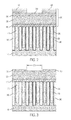
- FIG. 1 is a perspective diagram of a FinFET device showing a plurality of sacrificial gates disposed over semiconductor fins following a gate cut module;
- FIG. 2 is an inter-fin cross-sectional schematic diagram of an exemplary structure after forming a block mask including a hard mask layer over a plurality of sacrificial gates;
- FIG. 3 depicts etching of a portion of the block mask to define an opening having a first critical dimension
- FIG. 4 shows deposition of a conformal oxide spacer layer over the patterned block mask according to a comparative example
- FIG. 5 shows an idealized structure following an anisotropic etch of the oxide spacer layer of FIG. 4 and the attendant definition of an opening having a second critical dimension
- FIG. 6 shows a comparative structure following an anisotropic etch of the conformal oxide layer of FIG. 4 and the formation of an opening having a second critical dimension and including recessed regions within an interlayer dielectric adjacent to the sacrificial gates;
- FIG. 7 shows etching of exposed sacrificial gates within the opening to form gate cut openings that extend through the etched sacrificial gates and the deposition of a fill layer within both the gate cut openings and the recessed regions according to a comparative example
- FIG. 8 is an inter-fin cross-sectional schematic diagram of an exemplary structure following the definition of an opening having a first critical dimension and including recessed regions within an interlayer dielectric adjacent to the sacrificial gates;
- FIG. 9 shows deposition of a conformal oxide spacer layer over exposed sidewall surfaces of the hard mask and within the recessed regions
- FIG. 10 shows an anisotropic etch of the oxide spacer layer of FIG. 9 to define an opening having a second critical dimension and etching of exposed sacrificial gates to form gate cut openings that extend through the exposed sacrificial gates;
- FIG. 11 shows deposition of a fill layer within the gate cut openings and over the oxide layer disposed within the recessed regions.
- sacrificial gate segmentation includes the deposition of an oxide spacer layer after forming an opening through a block mask to expose the sacrificial gate within the opening.
- the oxide spacer layer can be used to control the critical dimension of the opening and the subsequent gate cut.
- segmentation includes providing a gate cut that is parallel to a length direction of the fins.
- FIG. 1 A simplified perspective view of a FinFET structure is shown in FIG. 1 .
- the exemplary structure includes a semiconductor substrate 100 and a plurality of semiconductor fins 120 arrayed over the substrate 100 .
- the semiconductor fins 120 are arranged in parallel and are laterally isolated from each other by a shallow trench isolation layer 140 , and raised source/drain junctions 610 are disposed over portions of the fins 120 proximate to top surfaces thereof.
- One or more layers of an interlayer dielectric 240 are disposed over the fins, i.e., over source/drain junctions 610 , and plural sacrificial gate structures 210 straddle the fins, i.e., over channel regions of the fins between source/drain junctions 610 .
- the sacrificial gate structures 210 have been segmented, or cut, to define discrete device regions. The cut regions have been backfilled with a fill layer 500 along a longitudinal direction in order to isolate the sacrificial gate structures 210 associated
- Substrate 100 may include a semiconductor material such as silicon, e.g., single crystal Si or polycrystalline Si, or a silicon-containing material.
- Silicon-containing materials include, but are not limited to, single crystal silicon germanium (SiGe), polycrystalline silicon germanium, silicon doped with carbon (Si:C), amorphous Si, as well as combinations and multi-layers thereof.
- SiGe single crystal silicon germanium
- Si:C silicon doped with carbon
- amorphous Si as well as combinations and multi-layers thereof.
- single crystal denotes a crystalline solid, in which the crystal lattice of the entire solid is substantially continuous and substantially unbroken to the edges of the solid with substantially no grain boundaries.
- the substrate 100 is not limited to silicon-containing materials, however, as the substrate 100 may comprise other semiconductor materials, including Ge and compound semiconductors, including III-V compound semiconductors such as GaAs, InAs, GaN, GaP, InSb, ZnSe, and ZnS, and II-VI compound semiconductors such as CdSe, CdS, CdTe, ZnSe, ZnS and ZnTe.
- III-V compound semiconductors such as GaAs, InAs, GaN, GaP, InSb, ZnSe, and ZnS
- II-VI compound semiconductors such as CdSe, CdS, CdTe, ZnSe, ZnS and ZnTe.
- Substrate 100 may be a bulk substrate or a composite substrate such as a semiconductor-on-insulator (SOI) substrate that comprises, from bottom to top, a handle portion, an isolation layer, and a semiconductor material layer.
- SOI semiconductor-on-insulator
- Substrate 100 may have dimensions as typically used in the art and may comprise, for example, a semiconductor wafer.
- Example wafer diameters include, but are not limited to, 50, 100, 150, 200, 300 and 450 mm.
- the total substrate thickness may range from 250 microns to 1500 microns, although in particular embodiments the substrate thickness is in the range of 725 to 775 microns, which corresponds to thickness dimensions commonly used in silicon CMOS processing.
- the semiconductor substrate 100 may comprise (100)-oriented silicon or (111)-oriented silicon, for example.
- fins 120 comprise a semiconductor material such as silicon, and may be formed by patterning and then etching the semiconductor substrate 100 , i.e., a top portion of the semiconductor substrate. In several embodiments, the fins 120 are etched from, and therefore contiguous with the semiconductor substrate 100 . For instance, fins 120 may be formed using a sidewall image transfer (SIT) process as known to those skilled in the art.
- SIT sidewall image transfer
- the fins 120 can have a width of 5 nm to 20 nm, and height of 40 nm to 150 nm, although other dimensions are contemplated. Fins 120 may be arrayed on the substrate at a regular intrafin spacing or pitch (d).
- pitch refers to the distance between one structure or feature (e.g., a first fin) and an adjacent structure or feature (e.g., a second fin).
- the fin pitch (d) may be within a range of 20 to 100 nm, e.g., 20, 30, 40, 50, 60, 70, 80, 90 or 100 nm, including ranges between any of the foregoing values, although smaller and larger pitch values may be used.
- a shallow trench isolation (STI) layer 140 may be used to provide electrical isolation between the fins 120 and between adjacent devices as is needed for the circuit(s) being implemented.
- An STI process for FinFET devices involves creating isolation trenches in the semiconductor substrate 100 through an anisotropic etch process. The isolation trench between each adjacent fin may have a relatively high aspect ratio (e.g., ratio of the depth of the isolation trench to its width).
- a dielectric filler material such as silicon dioxide, is deposited into the isolation trenches, for example, using an enhanced high aspect ratio process (eHARP) to fill the isolation trenches.
- the deposited dielectric material may then be polished by a chemical-mechanical polishing (CMP) process that removes the excess dielectric material and creates a planar STI structure.
- CMP chemical-mechanical polishing
- the planarized oxide may be etched back to form a recessed, uniformly thick oxide isolation layer 140 between the fins 120 , where upper sidewalls of the fins 120 are exposed for further processing.
- a sacrificial gate 210 is formed over the fins 120 and over the STI layer 140 .
- the sacrificial gate 210 may comprise polysilicon or amorphous silicon (a-Si), for example.
- Amorphous elemental silicon can be deposited using chemical vapor deposition, such as low pressure chemical vapor deposition (LPCVD) at temperatures ranging from 450° C. to 700° C.
- LPCVD low pressure chemical vapor deposition
- Silane (SiH 4 ) can be used as the precursor for CVD silicon deposition.
- the sacrificial gate 210 may have a thickness sufficient to straddle the top and sidewall surfaces of the fins.
- a thickness of sacrificial gate 210 may range from 50 to 200 nm, e.g., 50, 75, 100, 125, 150, 175 or 200 nm, including ranges between any of the foregoing values, although lesser and greater thicknesses may be used.
- a CMP process may be used to planarize a top surface of the sacrificial gate 210 .
- Planarization refers to a material removal process that employs at least mechanical forces, such as frictional media, to produce a substantially two-dimensional surface.
- a planarization process may include chemical mechanical polishing (CMP) or grinding.
- CMP chemical mechanical polishing
- CMP is a material removal process that uses both chemical reactions and mechanical forces to remove material and planarize a surface.
- a sacrificial oxide layer (not shown) may be deposited over the sacrificial gate 210 prior to a CMP step and then subsequently removed during the CMP step in order to enhance planarization.
- the sacrificial gate 210 may serve as a CMP etch stop.
- a non-selective etch such as a reactive ion etch (RIE) of the post-planarized sacrificial gate 210 may be used to define the thickness of the sacrificial gate 210 over the fins.
- RIE reactive ion etch
- sacrificial gate 210 is adapted to provide a temporary structure for a replacement metal gate (RMG) module wherein the sacrificial gate 210 is replaced by a functional gate structure.
- RMG replacement metal gate
- the processes used to segment the sacrificial gates include lithography, etching and the deposition of an etch-selective fill material that backfills removed portions of the sacrificial gate.
- the deposition of the fill material can negatively impact the removal of materials or layers later in the process flow, where the fill material acts as an unintended etch mask.
- an intra-fin cross-section view shows plural adjacent sacrificial gates 210 disposed over STI layer 140 .
- Sidewall spacers 220 are disposed over sidewalls (vertical surfaces) of the sacrificial gate 210 , and a conformal liner 230 is disposed over the sidewall spacers 220 .
- the conformal liner 230 is adapted to function as a contact etch stop layer (CESL).
- Sidewall spacers 220 may be formed by blanket deposition of a spacer material (e.g., using atomic layer deposition or chemical vapor deposition) followed by a directional etch such as reactive ion etching (RIE) to remove the spacer material from horizontal surfaces.
- RIE reactive ion etching
- the sidewall spacer thickness is 4 to 20 nm, e.g., 4, 10, 15 or 20 nm, including ranges between any of the foregoing values.
- the formation or deposition of a layer or structure may involve one or more techniques suitable for the material or layer being deposited or the structure being formed.
- Such techniques include, but are not limited to, chemical vapor deposition (CVD), low-pressure chemical vapor deposition (LPCVD), plasma enhanced chemical vapor deposition (PECVD), metal organic CVD (MOCVD), atomic layer deposition (ALD), molecular beam epitaxy (MBE), electroplating, electroless plating, ion beam deposition, and physical vapor deposition (PVD) techniques such as sputtering or evaporation.
- CVD chemical vapor deposition
- LPCVD low-pressure chemical vapor deposition
- PECVD plasma enhanced chemical vapor deposition
- MOCVD metal organic CVD
- ALD atomic layer deposition
- MBE molecular beam epitaxy
- electroplating electroless plating
- ion beam deposition ion beam deposition
- PVD physical vapor deposition
- Conformal liner 230 may be formed by blanket deposition of a suitable contact etch stop material (e.g., using atomic layer deposition). As seen with reference again to FIG. 1 , within the source/drain contact locations, the conformal liner 230 is formed over the sidewall spacers 220 as well as over the source/drain junctions 610 . In certain embodiments, the conformal liner 230 thickness is 2 to 10 nm, e.g., 2, 4, 6, 8 or 10 nm, including ranges between any of the foregoing values.
- Suitable sidewall spacer and conformal liner materials include oxides, nitrides and oxynitrides, such as silicon dioxide, silicon nitride, silicon oxynitride, as well as low dielectric constant (low-k) materials such as amorphous carbon, SiOC, SiOCN and SiBCN. As used herein, a low-k material has a dielectric constant less than that of silicon dioxide.
- the sidewall spacers 220 and the conformal liner 230 are formed from materials that can be etched selectively to one another.
- the sidewall spacers 220 comprises SiOCN and the conformal liner (i.e., contact etch stop layer) 230 comprises silicon nitride.
- an interlayer dielectric 240 is disposed between adjacent sacrificial gates 210 , i.e., directly over the conformal liner 230 .
- the interlayer dielectric 240 may comprise any dielectric material including, for example, oxides, nitrides, oxycarbides or oxynitrides.
- interlayer dielectric e.g., SiO 2
- the interlayer dielectric 240 can be planarized by chemical mechanical polishing (CMP) such that a top surface of the interlayer dielectric 240 is coplanar with a top surface of the sacrificial gates 210 .
- CMP chemical mechanical polishing
- the sacrificial gates 210 may serve as a CMP etch stop during removal of the excess interlayer dielectric 240 .
- Conformal liner 230 separates interlayer dielectric 240 from STI layer 140 .
- a block mask 300 including hard mask layer 310 , is formed over the device structure.
- Hard mask 310 may comprise silicon nitride, for example. Additional layers of the block mask include, from bottom to top, a spin on hard mask 320 , a nitride layer 330 , an anti-reflective coating 340 , and a photoresist layer 350 , which may be used to pattern the hard mask 320 over gate cut locations.
- a gate cut opening may be formed using patterning and etching processes known to those skilled in the art.
- the patterning process may comprise photolithography, for example.
- the photoresist layer 350 may include a positive-tone photoresist composition, a negative-tone photoresist composition, or a hybrid-tone photoresist composition.
- a layer of photoresist material may be formed by a deposition process such as, for example, spin-on coating.
- the deposited photoresist is then subjected to a pattern of irradiation, and the exposed photoresist material is developed utilizing a conventional resist developer.
- the pattern provided by the patterned photoresist material 350 is thereafter transferred into the hard mask 310 utilizing at least one pattern transfer etching process.
- the pattern transfer etching process is typically an anisotropic etch.
- a dry etching process such as, for example, reactive ion etching (RIE) can be used.
- RIE reactive ion etching
- a wet chemical etchant can be used.
- a combination of dry etching and wet etching can be used.
- the photoresist layer 350 is subjected to a pattern of irradiation, and the exposed photoresist material is developed utilizing a conventional resist developer. As shown in FIG. 2 , this provides a patterned layer of photoresist 350 atop the remaining layers of the block mask 300 . The pattern provided by the photoresist material is thereafter transferred into the nitride layer 330 and, as shown in FIG. 3 , the anti-reflective coating 340 and the photoresist layer 350 are then removed.
- the opening in the photoresist 350 and the corresponding opening in the nitride layer 330 may have a first critical dimension (CD1), which may span the width of one or more sacrificial gates 210 .
- the opening in the nitride layer 330 may have areal dimensions (length and width) that independently range from 30 to 40 nm, although lesser and greater dimensions may be used.
- the relatively large areal dimensions (e.g., CD1) of the as-formed opening in the nitride layer 330 are within lithography process windows for forming such structures.
- a conformal oxide layer 400 is formed over the nitride layer 330 and over the spin on hard mask 320 of block mask 300 , i.e., within the opening formed in the nitride layer 330 .
- formation of the oxide layer 400 includes a conformal deposition process such as a chemical vapor deposition (CVD) process.
- the thickness of the oxide layer may range from 10 to 20 nm, for example.
- the oxide layer 400 comprises silicon dioxide.
- Formation of the oxide layer 400 is followed by an anisotropic etch, such as a reactive ion etch, to remove the oxide layer from horizontal surfaces, which exposes a top surface of the nitride layer 330 .
- an anisotropic etch such as a reactive ion etch
- the oxide layer 400 remaining over the gate cut opening sidewalls can be used to tailor the areal dimensions (i.e., critical dimension(s)) of the gate cut openings.
- an intermediate gate cut opening is formed having a larger critical dimension (CD1), which is decreased by forming the oxide layer 400 on sidewalls of the intermediate opening.
- CD1 critical dimension
- the areal dimensions (length and width) of the gate cut openings that include the oxide layer 400 may independently range from 10 to 20 nm, e.g., 10, 15 or 20 nm, including ranges between any of the foregoing values.
- the remaining portions of the oxide layer 400 i.e., the oxide layer formed over sidewall surfaces of the nitride layer 330 , effectively decrease the size of the opening etched in the nitride layer 310 to a second critical dimension (CD2) less than the first critical dimension (CD1).
- CD2 second critical dimension
- CD1 first critical dimension
- FIG. 5 shows an idealized structure depicting etching through remaining portions of block mask 300 to define an opening 305 having a second critical dimension (CD2), where the etching exposes top surfaces of the sacrificial gates 210 and interlayer dielectric 240 .
- FIG. 6 shown is a comparative structure following an anisotropic etch through block mask 300 and the associated definition of opening 305 exposing top surfaces of the sacrificial gates 210 .
- the opening 305 has a second critical dimension (CD2) less than the first critical dimension (CD1) and, due to over etching of the interlayer dielectric 240 , includes recessed regions 245 that are formed within interlayer dielectric 240 laterally adjacent to the sacrificial gates. Within contacted regions of the structure, recessed regions 245 overlie source/drain regions of the device.
- Patterning for the opening 305 is configured to expose a portion of the STI layer 140 between adjacent fins without exposing the fins themselves.
- FIG. 7 shown is the etching within opening 305 of the exposed sacrificial gates 210 to form gate cut openings 215 that extend through the exposed structures, followed by the deposition of a fill layer 500 within the gate cut openings 215 and the recessed regions 245 .
- the fill layer completely fills the gate cut openings 215 .
- the fill layer 500 may be formed by atomic layer deposition (ALD) and may comprise a nitride compound such as silicon nitride.
- ALD atomic layer deposition
- a silicon-containing precursor and a nitrogen-containing precursor are deposited in succession and reacted to form a nitride fill layer.
- Fill layer 500 is adapted to serve as an etch-selective isolation layer that separates remaining sacrificial gate segments can be removed selective to the fill layer 500 and replaced with a functional gate.
- portions 501 of fill layer 500 located with recessed regions 245 may partially or wholly block later removal of the interlayer dielectric 240 from over source/drain junctions 610 during a SAC module.
- formation of oxide spacer layer 400 is delayed until after formation of openings 305 , such that recessed regions 245 are filled with an oxide rather than a nitride.
- Opening 305 has a first critical dimension (CD1) and includes recessed regions 245 within an interlayer dielectric 240 located adjacent to a sacrificial gate 210 .
- etching of the block mask 300 to form opening 305 precedes formation of an oxide spacer layer 400 .
- FIG. 9 shows removal of the nitride layer 330 and the spin on hard mask 320 from block mask 300 and deposition of a conformal oxide spacer layer 400 over hard mask 310 , including over exposed sidewall surfaces of the hard mask 310 within opening 305 .
- oxide spacer layer 400 is formed directly over sacrificial gate 210 and directly over interlayer dielectric 240 within recessed regions 245 .
- an anisotropic etch of the oxide spacer layer 400 defines an opening 305 in hard mask 310 having a second critical dimension (CD2). Following the anisotropic etch, remaining portions of the oxide spacer layer 400 are disposed over sidewall surfaces of the hard mask 310 within opening 305 and within recessed regions 245 , i.e., directly over interlayer dielectric 240 and directly over CESL layer 230 .
- Sacrificial gates 210 exposed within opening 305 are then etched to form gate cut openings 215 that extend through the structures.
- a fill layer 500 is deposited within the gate cut openings 215 and over the oxide layer 400 disposed within the recessed regions.
- oxide spacer layer 400 is formed within recessed regions and directly over interlayer dielectric 240 , a single oxide etching step may be used to expose source/drain junctions beneath oxide layer 400 , 240 .
- additional processing may be used to complete a device such as a FinFET, including the implementation of a replacement metal gate (RMG) module, which typically includes selective removal of the remaining (segmented) portions of the sacrificial gate, and the formation of a functional gate structure, including gate dielectric and gate conductor layers.
- RMG replacement metal gate
- device density and performance may be improved by forming an oxide spacer layer after forming an opening in a masking layer to expose top surfaces of the sacrificial gate.
- the disclosed methods enable the formation of sacrificial gate structures, and ultimately functional gate structures, having a small (e.g., less than 15 nm) cut dimension along a longitudinal direction, while also enabling a robust process for the downstream formation of source/drain contacts.
- the method may be implemented in conjunction with a replacement metal gate (RMG) module to address the formation of recessed regions within a dielectric layer located laterally adjacent to the sacrificial gates during formation of a patterned hard mask to define a gate cut location.
- RMG replacement metal gate
- an oxide spacer layer which may be used to adjust the critical dimension of a gate cut opening, is formed after etching the hard mask such that the oxide layer is deposited directly over the top surface of the sacrificial gate, onto sidewall surfaces of the hard mask, and into recessed regions located adjacent to the sacrificial gate.
- the opening of trenches the oxide layer and the dielectric layer to expose source/drain junctions is simplified.
Landscapes
- Engineering & Computer Science (AREA)
- Power Engineering (AREA)
- Microelectronics & Electronic Packaging (AREA)
- Physics & Mathematics (AREA)
- Condensed Matter Physics & Semiconductors (AREA)
- General Physics & Mathematics (AREA)
- Computer Hardware Design (AREA)
- Manufacturing & Machinery (AREA)
- Chemical & Material Sciences (AREA)
- Chemical Kinetics & Catalysis (AREA)
- Ceramic Engineering (AREA)
- General Chemical & Material Sciences (AREA)
- Inorganic Chemistry (AREA)
- General Engineering & Computer Science (AREA)
- Insulated Gate Type Field-Effect Transistor (AREA)
- Thin Film Transistor (AREA)
Abstract
Description
Claims (16)
Priority Applications (1)
| Application Number | Priority Date | Filing Date | Title |
|---|---|---|---|
| US15/643,940 US10396206B2 (en) | 2017-07-07 | 2017-07-07 | Gate cut method |
Applications Claiming Priority (1)
| Application Number | Priority Date | Filing Date | Title |
|---|---|---|---|
| US15/643,940 US10396206B2 (en) | 2017-07-07 | 2017-07-07 | Gate cut method |
Publications (2)
| Publication Number | Publication Date |
|---|---|
| US20190013245A1 US20190013245A1 (en) | 2019-01-10 |
| US10396206B2 true US10396206B2 (en) | 2019-08-27 |
Family
ID=64902856
Family Applications (1)
| Application Number | Title | Priority Date | Filing Date |
|---|---|---|---|
| US15/643,940 Active 2037-08-24 US10396206B2 (en) | 2017-07-07 | 2017-07-07 | Gate cut method |
Country Status (1)
| Country | Link |
|---|---|
| US (1) | US10396206B2 (en) |
Cited By (2)
| Publication number | Priority date | Publication date | Assignee | Title |
|---|---|---|---|---|
| US20190164772A1 (en) * | 2017-11-30 | 2019-05-30 | Taiwan Semiconductor Manufacturing Co., Ltd. | Method of patterning |
| US20200006531A1 (en) * | 2018-06-28 | 2020-01-02 | Taiwan Semiconductor Manufacturing Co., Ltd. | Method and device for forming cut-metal-gate feature |
Families Citing this family (8)
| Publication number | Priority date | Publication date | Assignee | Title |
|---|---|---|---|---|
| CN109216163A (en) * | 2017-06-29 | 2019-01-15 | 中芯国际集成电路制造(上海)有限公司 | The manufacturing method of semiconductor devices |
| US10396206B2 (en) * | 2017-07-07 | 2019-08-27 | Globalfoundries Inc. | Gate cut method |
| US11031290B2 (en) | 2017-11-30 | 2021-06-08 | Taiwan Semiconductor Manufacturing Co., Ltd. | Semiconductor structure with cutting depth control and method for fabricating the same |
| US10460994B2 (en) * | 2017-11-30 | 2019-10-29 | Taiwan Semiconductor Manufacturing Co., Ltd. | Residue-free metal gate cutting for fin-like field effect transistor |
| US10461171B2 (en) | 2018-01-12 | 2019-10-29 | Taiwan Semiconductor Manufacturing Co., Ltd. | Structure and formation method of semiconductor device with metal gate stacks |
| EP3621118A1 (en) * | 2018-09-07 | 2020-03-11 | IMEC vzw | A method for producing a gate cut structure on an array of semiconductor fins |
| CN112018034B (en) * | 2019-05-31 | 2023-12-12 | 中芯国际集成电路制造(上海)有限公司 | Semiconductor structure and forming method thereof |
| CN112582267A (en) * | 2019-09-30 | 2021-03-30 | 中芯国际集成电路制造(上海)有限公司 | Method for forming semiconductor device |
Citations (39)
| Publication number | Priority date | Publication date | Assignee | Title |
|---|---|---|---|---|
| US20120049286A1 (en) * | 2010-08-31 | 2012-03-01 | Globalfoundries Inc. | Gate Electrodes of a Semiconductor Device Formed by a Hard Mask and Double Exposure in Combination with a Shrink Spacer |
| US20130270644A1 (en) * | 2012-04-11 | 2013-10-17 | International Business Machines Corporation | Replacement gate structures and methods of manufacturing |
| US20140193974A1 (en) * | 2013-01-09 | 2014-07-10 | Taiwan Semiconductor Manufacturing Co., Ltd. | Multi-patterning method and device formed by the method |
| US9040405B2 (en) * | 2013-10-01 | 2015-05-26 | Globalfoundries Inc. | Gate electrode with a shrink spacer |
| US20150325482A1 (en) * | 2014-05-08 | 2015-11-12 | GlobalFoundries, Inc. | Integrated circuits having improved gate structures and methods for fabricating same |
| US9293459B1 (en) * | 2014-09-30 | 2016-03-22 | International Business Machines Corporation | Method and structure for improving finFET with epitaxy source/drain |
| US20160086947A1 (en) * | 2014-09-18 | 2016-03-24 | Panjae PARK | Semiconductor devices and methods for manufacturing the same |
| US20160111524A1 (en) * | 2014-10-17 | 2016-04-21 | Seungseok HA | Semiconductor devices including a gate core and a fin active core and methods of fabricating the same |
| US9331074B1 (en) * | 2015-01-30 | 2016-05-03 | Taiwan Semiconductor Manufacturing Co., Ltd. | Semiconductor device and manufacturing method thereof |
| US20160133632A1 (en) * | 2014-11-12 | 2016-05-12 | Hong-bae Park | Integrated circuit device and method of manufacturing the same |
| US20160148935A1 (en) * | 2014-11-26 | 2016-05-26 | Taiwan Semiconductor Manufacturing Co., Ltd. | Fin field effect transistor (finfet) device with controlled end-to-end critical dimension and method for forming the same |
| US9418868B1 (en) * | 2015-03-13 | 2016-08-16 | Taiwan Semiconductor Manufacturing Company, Ltd. | Method of fabricating semiconductor device with reduced trench distortions |
| US20160247728A1 (en) * | 2015-02-23 | 2016-08-25 | Junggun YOU | Method of fabricating semiconductor device |
| US9520482B1 (en) * | 2015-11-13 | 2016-12-13 | Taiwan Semiconductor Manufacturing Company, Ltd. | Method of cutting metal gate |
| US20160365424A1 (en) | 2015-06-15 | 2016-12-15 | International Business Machines Corporation | Self-aligned trench silicide process for preventing gate contact to silicide shorts |
| US20160379893A1 (en) | 2015-06-24 | 2016-12-29 | International Business Machines Corporation | Integrated circuit (ic) with offset gate sidewall contacts and method of manufacture |
| US9601567B1 (en) * | 2015-10-30 | 2017-03-21 | Taiwan Semiconductor Manufacturing Co., Ltd. | Multiple Fin FET structures having an insulating separation plug |
| US20170125411A1 (en) * | 2015-11-04 | 2017-05-04 | Taiwan Semiconductor Manufacturing Co., Ltd. | Semiconductor device and manufacturing method thereof |
| US20170141210A1 (en) * | 2015-11-16 | 2017-05-18 | Taiwan Semiconductor Manufacturing Company, Ltd. | Method of Cutting Metal Gate |
| US20170148682A1 (en) * | 2015-11-19 | 2017-05-25 | International Business Machines Corporation | Finfet with post-rmg gate cut |
| US20170256457A1 (en) * | 2016-03-04 | 2017-09-07 | Taiwan Semiconductor Manufacturing Co., Ltd. | Semiconductor structure and manufacturing method thereof |
| US20170278752A1 (en) * | 2016-03-15 | 2017-09-28 | Imec Vzw | Self-aligned gate contact |
| US9812365B1 (en) * | 2016-10-05 | 2017-11-07 | Globalfoundries Inc. | Methods of cutting gate structures on transistor devices |
| US20170330801A1 (en) * | 2016-05-11 | 2017-11-16 | Imec Vzw | Method of forming gate of semiconductor device and semiconductor device having same |
| US20170345913A1 (en) * | 2016-05-26 | 2017-11-30 | Globalfoundries Inc. | Methods for performing a gate cut last scheme for finfet semiconductor devices |
| US20170358585A1 (en) * | 2016-06-14 | 2017-12-14 | Globalfoundries Inc. | Method, apparatus and system for fabricating self-aligned contact using block-type hard mask |
| US9917103B1 (en) * | 2017-01-04 | 2018-03-13 | Globalfoundries Inc. | Diffusion break forming after source/drain forming and related IC structure |
| US20180096839A1 (en) * | 2016-10-04 | 2018-04-05 | Globalfoundries Inc. | Shrink process aware assist features |
| US20180108770A1 (en) * | 2016-10-17 | 2018-04-19 | International Business Machines Corporation | Self-aligned gate cut with polysilicon liner oxidation |
| US20180151442A1 (en) * | 2016-11-29 | 2018-05-31 | Taiwan Semiconductor Manufacturing Company, Ltd. | Semiconductor Device and Method of Manufacture |
| US20180182859A1 (en) * | 2016-12-22 | 2018-06-28 | Taiwan Semiconductor Manufacturing Co., Ltd. | Metal gate structure and methods thereof |
| US10056469B1 (en) * | 2017-02-13 | 2018-08-21 | Globalfoundries Inc. | Gate cut integration and related device |
| US20180261514A1 (en) * | 2017-03-10 | 2018-09-13 | Globalfoundries Inc. | Fin-type field effect transistors (finfets) with replacement metal gates and methods |
| US10083874B1 (en) * | 2017-03-23 | 2018-09-25 | Globalfoundries Inc. | Gate cut method |
| US10090169B1 (en) * | 2017-03-31 | 2018-10-02 | Globalfoundries Inc. | Methods of forming integrated circuit structures including opening filled with insulator in metal gate |
| US20190006345A1 (en) * | 2017-06-29 | 2019-01-03 | Taiwan Semiconductor Manufacturing Co., Ltd. | Metal gate structure cutting process |
| US20190013245A1 (en) * | 2017-07-07 | 2019-01-10 | Globalfoundries Inc. | Gate cut method |
| US10229854B1 (en) * | 2017-12-14 | 2019-03-12 | International Business Machines Corporation | FinFET gate cut after dummy gate removal |
| US10236213B1 (en) * | 2018-03-12 | 2019-03-19 | Globalfoundries Inc. | Gate cut structure with liner spacer and related method |
-
2017
- 2017-07-07 US US15/643,940 patent/US10396206B2/en active Active
Patent Citations (40)
| Publication number | Priority date | Publication date | Assignee | Title |
|---|---|---|---|---|
| US20120049286A1 (en) * | 2010-08-31 | 2012-03-01 | Globalfoundries Inc. | Gate Electrodes of a Semiconductor Device Formed by a Hard Mask and Double Exposure in Combination with a Shrink Spacer |
| US20130270644A1 (en) * | 2012-04-11 | 2013-10-17 | International Business Machines Corporation | Replacement gate structures and methods of manufacturing |
| US20140193974A1 (en) * | 2013-01-09 | 2014-07-10 | Taiwan Semiconductor Manufacturing Co., Ltd. | Multi-patterning method and device formed by the method |
| US9040405B2 (en) * | 2013-10-01 | 2015-05-26 | Globalfoundries Inc. | Gate electrode with a shrink spacer |
| US20150325482A1 (en) * | 2014-05-08 | 2015-11-12 | GlobalFoundries, Inc. | Integrated circuits having improved gate structures and methods for fabricating same |
| US20160086947A1 (en) * | 2014-09-18 | 2016-03-24 | Panjae PARK | Semiconductor devices and methods for manufacturing the same |
| US9293459B1 (en) * | 2014-09-30 | 2016-03-22 | International Business Machines Corporation | Method and structure for improving finFET with epitaxy source/drain |
| US20160111524A1 (en) * | 2014-10-17 | 2016-04-21 | Seungseok HA | Semiconductor devices including a gate core and a fin active core and methods of fabricating the same |
| US20160133632A1 (en) * | 2014-11-12 | 2016-05-12 | Hong-bae Park | Integrated circuit device and method of manufacturing the same |
| US20160148935A1 (en) * | 2014-11-26 | 2016-05-26 | Taiwan Semiconductor Manufacturing Co., Ltd. | Fin field effect transistor (finfet) device with controlled end-to-end critical dimension and method for forming the same |
| US9935103B2 (en) * | 2015-01-30 | 2018-04-03 | Taiwan Semiconductor Manufacturing Co., Ltd. | Semiconductor device and manufacturing method thereof |
| US9331074B1 (en) * | 2015-01-30 | 2016-05-03 | Taiwan Semiconductor Manufacturing Co., Ltd. | Semiconductor device and manufacturing method thereof |
| US20160247728A1 (en) * | 2015-02-23 | 2016-08-25 | Junggun YOU | Method of fabricating semiconductor device |
| US9418868B1 (en) * | 2015-03-13 | 2016-08-16 | Taiwan Semiconductor Manufacturing Company, Ltd. | Method of fabricating semiconductor device with reduced trench distortions |
| US20160365424A1 (en) | 2015-06-15 | 2016-12-15 | International Business Machines Corporation | Self-aligned trench silicide process for preventing gate contact to silicide shorts |
| US20160379893A1 (en) | 2015-06-24 | 2016-12-29 | International Business Machines Corporation | Integrated circuit (ic) with offset gate sidewall contacts and method of manufacture |
| US9601567B1 (en) * | 2015-10-30 | 2017-03-21 | Taiwan Semiconductor Manufacturing Co., Ltd. | Multiple Fin FET structures having an insulating separation plug |
| US20170125411A1 (en) * | 2015-11-04 | 2017-05-04 | Taiwan Semiconductor Manufacturing Co., Ltd. | Semiconductor device and manufacturing method thereof |
| US9520482B1 (en) * | 2015-11-13 | 2016-12-13 | Taiwan Semiconductor Manufacturing Company, Ltd. | Method of cutting metal gate |
| US20170141210A1 (en) * | 2015-11-16 | 2017-05-18 | Taiwan Semiconductor Manufacturing Company, Ltd. | Method of Cutting Metal Gate |
| US20170148682A1 (en) * | 2015-11-19 | 2017-05-25 | International Business Machines Corporation | Finfet with post-rmg gate cut |
| US20170256457A1 (en) * | 2016-03-04 | 2017-09-07 | Taiwan Semiconductor Manufacturing Co., Ltd. | Semiconductor structure and manufacturing method thereof |
| US20170278752A1 (en) * | 2016-03-15 | 2017-09-28 | Imec Vzw | Self-aligned gate contact |
| US20170330801A1 (en) * | 2016-05-11 | 2017-11-16 | Imec Vzw | Method of forming gate of semiconductor device and semiconductor device having same |
| US20170345913A1 (en) * | 2016-05-26 | 2017-11-30 | Globalfoundries Inc. | Methods for performing a gate cut last scheme for finfet semiconductor devices |
| US20170358585A1 (en) * | 2016-06-14 | 2017-12-14 | Globalfoundries Inc. | Method, apparatus and system for fabricating self-aligned contact using block-type hard mask |
| US20180096839A1 (en) * | 2016-10-04 | 2018-04-05 | Globalfoundries Inc. | Shrink process aware assist features |
| US9812365B1 (en) * | 2016-10-05 | 2017-11-07 | Globalfoundries Inc. | Methods of cutting gate structures on transistor devices |
| US20180108770A1 (en) * | 2016-10-17 | 2018-04-19 | International Business Machines Corporation | Self-aligned gate cut with polysilicon liner oxidation |
| US20180151442A1 (en) * | 2016-11-29 | 2018-05-31 | Taiwan Semiconductor Manufacturing Company, Ltd. | Semiconductor Device and Method of Manufacture |
| US20180182859A1 (en) * | 2016-12-22 | 2018-06-28 | Taiwan Semiconductor Manufacturing Co., Ltd. | Metal gate structure and methods thereof |
| US9917103B1 (en) * | 2017-01-04 | 2018-03-13 | Globalfoundries Inc. | Diffusion break forming after source/drain forming and related IC structure |
| US10056469B1 (en) * | 2017-02-13 | 2018-08-21 | Globalfoundries Inc. | Gate cut integration and related device |
| US20180261514A1 (en) * | 2017-03-10 | 2018-09-13 | Globalfoundries Inc. | Fin-type field effect transistors (finfets) with replacement metal gates and methods |
| US10083874B1 (en) * | 2017-03-23 | 2018-09-25 | Globalfoundries Inc. | Gate cut method |
| US10090169B1 (en) * | 2017-03-31 | 2018-10-02 | Globalfoundries Inc. | Methods of forming integrated circuit structures including opening filled with insulator in metal gate |
| US20190006345A1 (en) * | 2017-06-29 | 2019-01-03 | Taiwan Semiconductor Manufacturing Co., Ltd. | Metal gate structure cutting process |
| US20190013245A1 (en) * | 2017-07-07 | 2019-01-10 | Globalfoundries Inc. | Gate cut method |
| US10229854B1 (en) * | 2017-12-14 | 2019-03-12 | International Business Machines Corporation | FinFET gate cut after dummy gate removal |
| US10236213B1 (en) * | 2018-03-12 | 2019-03-19 | Globalfoundries Inc. | Gate cut structure with liner spacer and related method |
Cited By (5)
| Publication number | Priority date | Publication date | Assignee | Title |
|---|---|---|---|---|
| US20190164772A1 (en) * | 2017-11-30 | 2019-05-30 | Taiwan Semiconductor Manufacturing Co., Ltd. | Method of patterning |
| US11901190B2 (en) * | 2017-11-30 | 2024-02-13 | Taiwan Semiconductor Manufacturing Company, Ltd. | Method of patterning |
| US20200006531A1 (en) * | 2018-06-28 | 2020-01-02 | Taiwan Semiconductor Manufacturing Co., Ltd. | Method and device for forming cut-metal-gate feature |
| US10950713B2 (en) * | 2018-06-28 | 2021-03-16 | Taiwan Semiconductor Manufacturing Co., Ltd. | Method and device for forming cut-metal-gate feature |
| US11557660B2 (en) * | 2018-06-28 | 2023-01-17 | Taiwan Semiconductor Manufacturing Co., Ltd. | Method and device for forming cut-metal-gate feature |
Also Published As
| Publication number | Publication date |
|---|---|
| US20190013245A1 (en) | 2019-01-10 |
Similar Documents
| Publication | Publication Date | Title |
|---|---|---|
| US10396206B2 (en) | Gate cut method | |
| US10083874B1 (en) | Gate cut method | |
| US10593803B2 (en) | Self-aligned shallow trench isolation and doping for vertical fin transistors | |
| US20190067115A1 (en) | Gate cut method for replacement metal gate | |
| US10991795B2 (en) | Semiconductor device and manufacturing method thereof | |
| US8722472B2 (en) | Hybrid CMOS nanowire mesh device and FINFET device | |
| US9818836B1 (en) | Gate cut method for replacement metal gate integration | |
| US8709888B2 (en) | Hybrid CMOS nanowire mesh device and PDSOI device | |
| US11469146B2 (en) | Methods of performing fin cut etch processes for FinFET semiconductor devices | |
| US20130153997A1 (en) | Hybrid cmos nanowire mesh device and bulk cmos device | |
| US10586860B2 (en) | Method of manufacturing finfet devices using narrow and wide gate cut openings in conjunction with a replacement metal gate process | |
| US10658506B2 (en) | Fin cut last method for forming a vertical FinFET device | |
| US20190139830A1 (en) | Self-aligned gate isolation | |
| US10083878B1 (en) | Fin fabrication process with dual shallow trench isolation and tunable inner and outer fin profile | |
| US20220375788A1 (en) | Formation of trench silicide source or drain contacts without gate damage | |
| US20150123211A1 (en) | NARROW DIFFUSION BREAK FOR A FIN FIELD EFFECT (FinFET) TRANSISTOR DEVICE | |
| US10373873B1 (en) | Gate cut in replacement metal gate process | |
| US10147648B1 (en) | Vertical fin gate structure for RF device | |
| US10002793B1 (en) | Sub-fin doping method | |
| US20230022802A1 (en) | Buried power rail contact | |
| US10593555B2 (en) | Composite sacrificial gate with etch selective layer |
Legal Events
| Date | Code | Title | Description |
|---|---|---|---|
| AS | Assignment |
Owner name: GLOBALFOUNDRIES INC., CAYMAN ISLANDS Free format text: ASSIGNMENT OF ASSIGNORS INTEREST;ASSIGNORS:JHA, ASHISH KUMAR;WANG, HAITING;HONG, WEI;AND OTHERS;SIGNING DATES FROM 20170627 TO 20170629;REEL/FRAME:042932/0256 |
|
| STPP | Information on status: patent application and granting procedure in general |
Free format text: RESPONSE TO NON-FINAL OFFICE ACTION ENTERED AND FORWARDED TO EXAMINER |
|
| STPP | Information on status: patent application and granting procedure in general |
Free format text: NOTICE OF ALLOWANCE MAILED -- APPLICATION RECEIVED IN OFFICE OF PUBLICATIONS |
|
| AS | Assignment |
Owner name: GLOBALFOUNDRIES INC., CAYMAN ISLANDS Free format text: ASSIGNMENT OF ASSIGNORS INTEREST;ASSIGNORS:JHA, ASHISH KUMAR;WANG, HAITING;HONG, WEI;AND OTHERS;SIGNING DATES FROM 20170627 TO 20190614;REEL/FRAME:049533/0288 |
|
| STPP | Information on status: patent application and granting procedure in general |
Free format text: PUBLICATIONS -- ISSUE FEE PAYMENT VERIFIED |
|
| STCF | Information on status: patent grant |
Free format text: PATENTED CASE |
|
| AS | Assignment |
Owner name: GLOBALFOUNDRIES U.S. INC., CALIFORNIA Free format text: ASSIGNMENT OF ASSIGNORS INTEREST;ASSIGNOR:GLOBALFOUNDRIES INC.;REEL/FRAME:054633/0001 Effective date: 20201022 |
|
| AS | Assignment |
Owner name: GLOBALFOUNDRIES U.S. INC., NEW YORK Free format text: RELEASE BY SECURED PARTY;ASSIGNOR:WILMINGTON TRUST, NATIONAL ASSOCIATION;REEL/FRAME:056987/0001 Effective date: 20201117 |
|
| MAFP | Maintenance fee payment |
Free format text: PAYMENT OF MAINTENANCE FEE, 4TH YEAR, LARGE ENTITY (ORIGINAL EVENT CODE: M1551); ENTITY STATUS OF PATENT OWNER: LARGE ENTITY Year of fee payment: 4 |