US10392359B2 - Compound for organic electric element, organic electric element comprising the same and electronic device thereof - Google Patents
Compound for organic electric element, organic electric element comprising the same and electronic device thereof Download PDFInfo
- Publication number
- US10392359B2 US10392359B2 US15/558,805 US201615558805A US10392359B2 US 10392359 B2 US10392359 B2 US 10392359B2 US 201615558805 A US201615558805 A US 201615558805A US 10392359 B2 US10392359 B2 US 10392359B2
- Authority
- US
- United States
- Prior art keywords
- group
- sub
- mmol
- com
- ring
- Prior art date
- Legal status (The legal status is an assumption and is not a legal conclusion. Google has not performed a legal analysis and makes no representation as to the accuracy of the status listed.)
- Active
Links
- 0 CCN(CC)C1=CC(CC(C)(C)C)=CC(N(CC)CC)=C1.[1*]C1=C([2*])C=C([3*])C2=C1CC1=C([4*])C([5*])=C([6*])C([7*])=C12 Chemical compound CCN(CC)C1=CC(CC(C)(C)C)=CC(N(CC)CC)=C1.[1*]C1=C([2*])C=C([3*])C2=C1CC1=C([4*])C([5*])=C([6*])C([7*])=C12 0.000 description 18
- ASHKEPPDOQVAOE-UHFFFAOYSA-N C1=CC2=C(C=C1)C1=C(C=CC=C1)C2.C1=CC2=C(C=C1)C1=C(C=CC=C1)C2.C1=CC2=C(C=C1)C1=C(C=CC=C1)C2.C1=CC2=C(C=C1)C1=C(C=CC=C1)C2.C1=CC2=C(C=C1)C1=C(C=CC=C1)C2.C1=CC2=C(C=C1)C1=C(C=CC=C1)C2.C1=CC2=C(C=C1)C1=C(C=CC=C1)C2.CC.CC.CC.CC.CC.CC.CC.CC.CC.CC.CC.CC.CC.CC.CCN(CC)C1=CC(CC(C)(C)C)=CC(N(CC)CC)=C1.CCN(CC)C1=CC(CC(C)(C)C)=CC(N(CC)CC)=C1 Chemical compound C1=CC2=C(C=C1)C1=C(C=CC=C1)C2.C1=CC2=C(C=C1)C1=C(C=CC=C1)C2.C1=CC2=C(C=C1)C1=C(C=CC=C1)C2.C1=CC2=C(C=C1)C1=C(C=CC=C1)C2.C1=CC2=C(C=C1)C1=C(C=CC=C1)C2.C1=CC2=C(C=C1)C1=C(C=CC=C1)C2.C1=CC2=C(C=C1)C1=C(C=CC=C1)C2.CC.CC.CC.CC.CC.CC.CC.CC.CC.CC.CC.CC.CC.CC.CCN(CC)C1=CC(CC(C)(C)C)=CC(N(CC)CC)=C1.CCN(CC)C1=CC(CC(C)(C)C)=CC(N(CC)CC)=C1 ASHKEPPDOQVAOE-UHFFFAOYSA-N 0.000 description 2
- BWERRBMPFGMBJN-UHFFFAOYSA-N C1=CC2=C(C=C1)C1=C(C=CC=C1)C2.C1=CC2=C(C=C1)C1=C(C=CC=C1)C2.C1=CC2=C(C=C1)C1=C(C=CC=C1)C2.C1=CC2=C(C=C1)C1=C(C=CC=C1)C2.C1=CC2=C(C=C1)C1=C(C=CC=C1)C2.CC.CC.CC.CC.CC.CC.CC.CC.CC.CC.CCN(CC)C1=CC(CC(C)(C)C)=CC(N(CC)CC)=C1.CCN(CC)C1=CC(CC(C)(C)C)=CC(N(CC)CC)=C1.CCN(CC)C1=CC(CC(C)(C)C)=CC(N(CC)CC)=C1 Chemical compound C1=CC2=C(C=C1)C1=C(C=CC=C1)C2.C1=CC2=C(C=C1)C1=C(C=CC=C1)C2.C1=CC2=C(C=C1)C1=C(C=CC=C1)C2.C1=CC2=C(C=C1)C1=C(C=CC=C1)C2.C1=CC2=C(C=C1)C1=C(C=CC=C1)C2.CC.CC.CC.CC.CC.CC.CC.CC.CC.CC.CCN(CC)C1=CC(CC(C)(C)C)=CC(N(CC)CC)=C1.CCN(CC)C1=CC(CC(C)(C)C)=CC(N(CC)CC)=C1.CCN(CC)C1=CC(CC(C)(C)C)=CC(N(CC)CC)=C1 BWERRBMPFGMBJN-UHFFFAOYSA-N 0.000 description 2
- QAMIWEBASJWBRN-UHFFFAOYSA-N C1=CC2=C(C=C1)C=C(N(C1=CC(C3=CC4=C(C=C3)C3=C(C=CC=C3)S4)=CC(N(C3=CC4=C(C=CC=C4)C=C3)C3=CC4=C(C=C3)C3=C(C=CC=C3)S4)=C1)C1=CC3=C(C=CC=C3)C=C1)C=C2.C1=CC2=CC=CC(N(C3=CC(N(C4=CC=CC5=C4C=CC=C5)C4=CC=CC5=C4C=CC=C5)=CC(C4=CC5=C(C=C4)C4=C(C=CC=C4)O5)=C3)C3=C4C=CC=CC4=CC=C3)=C2C=C1.C1=CC=C(C2=CC=C(N(C3=CC=CC=C3)C3=CC(C4=CC5=C(C=C4)C4=C(C=CC=C4)O5)=CC(N(C4=CC=CC=C4)C4=CC=CC=C4)=C3)C=C2)C=C1 Chemical compound C1=CC2=C(C=C1)C=C(N(C1=CC(C3=CC4=C(C=C3)C3=C(C=CC=C3)S4)=CC(N(C3=CC4=C(C=CC=C4)C=C3)C3=CC4=C(C=C3)C3=C(C=CC=C3)S4)=C1)C1=CC3=C(C=CC=C3)C=C1)C=C2.C1=CC2=CC=CC(N(C3=CC(N(C4=CC=CC5=C4C=CC=C5)C4=CC=CC5=C4C=CC=C5)=CC(C4=CC5=C(C=C4)C4=C(C=CC=C4)O5)=C3)C3=C4C=CC=CC4=CC=C3)=C2C=C1.C1=CC=C(C2=CC=C(N(C3=CC=CC=C3)C3=CC(C4=CC5=C(C=C4)C4=C(C=CC=C4)O5)=CC(N(C4=CC=CC=C4)C4=CC=CC=C4)=C3)C=C2)C=C1 QAMIWEBASJWBRN-UHFFFAOYSA-N 0.000 description 2
- WGLBOSSODXKXAQ-UHFFFAOYSA-N C1=CC2=CC=C(N(C3=CC(N(C4=CC5=C(C=CC=C5)C=C4)C4=CC5=C(C=CC=C5)C=C4)=CC(C4=C5SC6=C(C=CC=C6)C5=CC=C4)=C3)C3=CC4=C(C=CC=C4)C=C3)C=C2C=C1.C1=CC=C(C2=CC=C(N(C3=CC=C(C4=CC=CC=C4)C=C3)C3=CC(C4=C5OC6=C(C=CC=C6)C5=CC=C4)=CC(N(C4=CC=C(C5=CC=CC=C5)C=C4)C4=CC=C(C5=CC=CC=C5)C=C4)=C3)C=C2)C=C1.C1=CC=C(N(C2=CC=CC=C2)C2=CC(C3=C4OC5=C(C=CC=C5)C4=CC=C3)=CC(N(C3=CC=CC=C3)C3=CC=CC=C3)=C2)C=C1 Chemical compound C1=CC2=CC=C(N(C3=CC(N(C4=CC5=C(C=CC=C5)C=C4)C4=CC5=C(C=CC=C5)C=C4)=CC(C4=C5SC6=C(C=CC=C6)C5=CC=C4)=C3)C3=CC4=C(C=CC=C4)C=C3)C=C2C=C1.C1=CC=C(C2=CC=C(N(C3=CC=C(C4=CC=CC=C4)C=C3)C3=CC(C4=C5OC6=C(C=CC=C6)C5=CC=C4)=CC(N(C4=CC=C(C5=CC=CC=C5)C=C4)C4=CC=C(C5=CC=CC=C5)C=C4)=C3)C=C2)C=C1.C1=CC=C(N(C2=CC=CC=C2)C2=CC(C3=C4OC5=C(C=CC=C5)C4=CC=C3)=CC(N(C3=CC=CC=C3)C3=CC=CC=C3)=C2)C=C1 WGLBOSSODXKXAQ-UHFFFAOYSA-N 0.000 description 2
- FUKFBUYGSXQBIF-UHFFFAOYSA-N C1=CC=C(C2=C(N(C3=CC=CC=C3)C3=CC(C4=C5C(=CC=C4)SC4=C5C=CC5=C4C=CC=C5)=CC(N(C4=CC=CC=C4)C4=C(C5=CC=CC=C5)C=CC=C4)=C3)C=CC=C2)C=C1.C1=CC=C(N(C2=CC(N(C3=CC=CC=C3)C3=C4\C=CC=C\C4=C\C=C\3)=CC(C3=C4C(=CC=C3)OC3=C4C=CC4=C3C=CC=C4)=C2)C2=C3C(=CC=C2)C(C2=CC=CC=C2)(C2=CC=CC=C2)C2=C3C=CC=C2)C=C1.CC1(C)C2=CC(N(C3=CC=C4C(=C3)C(C)(C)C3=C4C=CC=C3)C3=CC(C4=CC=CC(C5=CC6=C(C=C5)C5=C(S6)C6=C(C=CC=C6)C6=C5C=CC=C6)=C4)=CC(N(C4=CC5=C(C=C4)C4=C(C=CC=C4)C5(C)C)C4=CC5=C(C=C4)C4=C(C=CC=C4)C5(C)C)=C3)=CC=C2C2=C1C=CC=C2 Chemical compound C1=CC=C(C2=C(N(C3=CC=CC=C3)C3=CC(C4=C5C(=CC=C4)SC4=C5C=CC5=C4C=CC=C5)=CC(N(C4=CC=CC=C4)C4=C(C5=CC=CC=C5)C=CC=C4)=C3)C=CC=C2)C=C1.C1=CC=C(N(C2=CC(N(C3=CC=CC=C3)C3=C4\C=CC=C\C4=C\C=C\3)=CC(C3=C4C(=CC=C3)OC3=C4C=CC4=C3C=CC=C4)=C2)C2=C3C(=CC=C2)C(C2=CC=CC=C2)(C2=CC=CC=C2)C2=C3C=CC=C2)C=C1.CC1(C)C2=CC(N(C3=CC=C4C(=C3)C(C)(C)C3=C4C=CC=C3)C3=CC(C4=CC=CC(C5=CC6=C(C=C5)C5=C(S6)C6=C(C=CC=C6)C6=C5C=CC=C6)=C4)=CC(N(C4=CC5=C(C=C4)C4=C(C=CC=C4)C5(C)C)C4=CC5=C(C=C4)C4=C(C=CC=C4)C5(C)C)=C3)=CC=C2C2=C1C=CC=C2 FUKFBUYGSXQBIF-UHFFFAOYSA-N 0.000 description 2
- RGIFXYGYRLOFHW-UHFFFAOYSA-N C1=CC=C(C2=CC=C(C3=CC=C(N(C4=CC=CC=C4)C4=CC(C5=C6C(=CC=C5)SC5=C6C=CC6=C5C=CC=C6)=CC(N(C5=CC=CC=C5)C5=CC=C(C6=CC=C(C7=CC=CC=C7)C=C6)C=C5)=C4)C=C3)C=C2)C=C1.C1=CC=C(N(C2=CC=CC=C2)C2=CC(/C3=C/C4=C(C=CC(C5=C6C(=CC=C5)OC5=C6C=CC6=C5C=CC=C6)=C4)S3)=CC(N(C3=CC=CC=C3)C3=C4C=CC=CC4=C(C4=CC=CC=N4)C=C3)=C2)C=C1.COC1=CC=C(N(C2=CC=C(OC)C=C2)C2=CC(C3=C4C(=CC=C3)SC3=C4C4=C(C=CC=C4)C=C3)=CC(N(C3=CC=C(OC)C=C3)C3=CC(OC)=CC=C3)=C2)C=C1 Chemical compound C1=CC=C(C2=CC=C(C3=CC=C(N(C4=CC=CC=C4)C4=CC(C5=C6C(=CC=C5)SC5=C6C=CC6=C5C=CC=C6)=CC(N(C5=CC=CC=C5)C5=CC=C(C6=CC=C(C7=CC=CC=C7)C=C6)C=C5)=C4)C=C3)C=C2)C=C1.C1=CC=C(N(C2=CC=CC=C2)C2=CC(/C3=C/C4=C(C=CC(C5=C6C(=CC=C5)OC5=C6C=CC6=C5C=CC=C6)=C4)S3)=CC(N(C3=CC=CC=C3)C3=C4C=CC=CC4=C(C4=CC=CC=N4)C=C3)=C2)C=C1.COC1=CC=C(N(C2=CC=C(OC)C=C2)C2=CC(C3=C4C(=CC=C3)SC3=C4C4=C(C=CC=C4)C=C3)=CC(N(C3=CC=C(OC)C=C3)C3=CC(OC)=CC=C3)=C2)C=C1 RGIFXYGYRLOFHW-UHFFFAOYSA-N 0.000 description 2
- DKFXBFRFKXMVOZ-UHFFFAOYSA-N C1=CC=C(C2=CC=C(C3=CC=CC(N(C4=CC=CC=C4)C4=CC(N(C5=CC=CC=C5)C5=CC=CC=C5)=CC(/C5=C/C6=C(C=CC(C7=C8\C9=C(C=CC%10=C9C=CC=C%10)S\C8=C\C=C\7)=C6)O5)=C4)=C3)C=C2)C=C1.C1=CC=C(C2=CC=C(N(C3=CC=CC=C3)C3=CC(C4=C5C(=CC=C4)OC4=C5C5=C(C=CC=C5)C=C4)=CC(N(C4=CC=CC=C4)C4=CC=C(C5=CC6=C(C=C5)SC=C6)C=C4)=C3)C=C2)C=C1.CC1=C(N(C2=CC(N(C3=CC=CC=C3)C3=CC=CC=C3)=CC(C3=C4C(=CC=C3)OC3=C4C4=C(C=CC=C4)C=C3)=C2)C2=C(C)C=CC=C2)C=CC=C1 Chemical compound C1=CC=C(C2=CC=C(C3=CC=CC(N(C4=CC=CC=C4)C4=CC(N(C5=CC=CC=C5)C5=CC=CC=C5)=CC(/C5=C/C6=C(C=CC(C7=C8\C9=C(C=CC%10=C9C=CC=C%10)S\C8=C\C=C\7)=C6)O5)=C4)=C3)C=C2)C=C1.C1=CC=C(C2=CC=C(N(C3=CC=CC=C3)C3=CC(C4=C5C(=CC=C4)OC4=C5C5=C(C=CC=C5)C=C4)=CC(N(C4=CC=CC=C4)C4=CC=C(C5=CC6=C(C=C5)SC=C6)C=C4)=C3)C=C2)C=C1.CC1=C(N(C2=CC(N(C3=CC=CC=C3)C3=CC=CC=C3)=CC(C3=C4C(=CC=C3)OC3=C4C4=C(C=CC=C4)C=C3)=C2)C2=C(C)C=CC=C2)C=CC=C1 DKFXBFRFKXMVOZ-UHFFFAOYSA-N 0.000 description 2
- VMZHWHPKFBUZTA-UHFFFAOYSA-N C1=CC=C(C2=CC=C(N(C3=CC=C(C4=CC=CC=C4)C=C3)C3=CC(C4=CC=C5C(=C4)SC4=C5C=CC=C4)=CC(N(C4=CC=C(C5=CC=CC=C5)C=C4)C4=CC=C(C5=CC=CC=C5)C=C4)=C3)C=C2)C=C1.C1=CC=C(C2=CC=C(N(C3=CC=CC=C3)C3=CC(C4=CC=C5C(=C4)SC4=C5C=CC=C4)=CC(N(C4=CC=CC=C4)C4=CC=C(C5=CC=CC=C5)C=C4)=C3)C=C2)C=C1.C1=CC=C(N(C2=CC=CC=C2)C2=CC(N(C3=CC=CC=C3)C3=CC4=C(C=C3)SC3=C4C=CC=C3)=CC(C3=CC=C4C(=C3)SC3=C4C=CC=C3)=C2)C=C1 Chemical compound C1=CC=C(C2=CC=C(N(C3=CC=C(C4=CC=CC=C4)C=C3)C3=CC(C4=CC=C5C(=C4)SC4=C5C=CC=C4)=CC(N(C4=CC=C(C5=CC=CC=C5)C=C4)C4=CC=C(C5=CC=CC=C5)C=C4)=C3)C=C2)C=C1.C1=CC=C(C2=CC=C(N(C3=CC=CC=C3)C3=CC(C4=CC=C5C(=C4)SC4=C5C=CC=C4)=CC(N(C4=CC=CC=C4)C4=CC=C(C5=CC=CC=C5)C=C4)=C3)C=C2)C=C1.C1=CC=C(N(C2=CC=CC=C2)C2=CC(N(C3=CC=CC=C3)C3=CC4=C(C=C3)SC3=C4C=CC=C3)=CC(C3=CC=C4C(=C3)SC3=C4C=CC=C3)=C2)C=C1 VMZHWHPKFBUZTA-UHFFFAOYSA-N 0.000 description 2
- ITEBHDWWVUJLHV-FCWKJLHSSA-N C1=CC=C(C2=CC=C(N(C3=CC=C(C4=CC=CC=C4)C=C3)C3=CC(N(C4=CC=C5C=CC=CC5=C4)C4=CC=C5C=CC=CC5=C4)=CC(C4=CC(C5=CC=CC6=C5OC5=C6C=CC=C5)=CC=C4)=C3)C=C2)C=C1.C1=CC=C(N(C2=CC=CC=C2)C2=CC(C3=CC=C(C4=CC=C(C5=CC=CC6=C5SC5=C6C=CC=C5)C=C4)C=C3)=CC(N(C3=CC4=C(C=C3)C3=C(C=CC=C3)O4)C3=CC4=C(C=C3)C3=C(C=CC=C3)O4)=C2)C=C1.[2H]C1=C([2H])C([2H])=C(C2=CC=C(N(C3=CC=CC=C3)C3=CC(C4=CC(/C5=C/C=C\C6=C5SC5=C6C=CC=C5)=CC=C4)=CC(N(C4=CC=CC=C4)C4=CC=C5C(=C4)C4(C6=C5C=CC=C6)C5=C(C=CC=C5)C5=C4C=CC=C5)=C3)C=C2)C([2H])=C1[2H] Chemical compound C1=CC=C(C2=CC=C(N(C3=CC=C(C4=CC=CC=C4)C=C3)C3=CC(N(C4=CC=C5C=CC=CC5=C4)C4=CC=C5C=CC=CC5=C4)=CC(C4=CC(C5=CC=CC6=C5OC5=C6C=CC=C5)=CC=C4)=C3)C=C2)C=C1.C1=CC=C(N(C2=CC=CC=C2)C2=CC(C3=CC=C(C4=CC=C(C5=CC=CC6=C5SC5=C6C=CC=C5)C=C4)C=C3)=CC(N(C3=CC4=C(C=C3)C3=C(C=CC=C3)O4)C3=CC4=C(C=C3)C3=C(C=CC=C3)O4)=C2)C=C1.[2H]C1=C([2H])C([2H])=C(C2=CC=C(N(C3=CC=CC=C3)C3=CC(C4=CC(/C5=C/C=C\C6=C5SC5=C6C=CC=C5)=CC=C4)=CC(N(C4=CC=CC=C4)C4=CC=C5C(=C4)C4(C6=C5C=CC=C6)C5=C(C=CC=C5)C5=C4C=CC=C5)=C3)C=C2)C([2H])=C1[2H] ITEBHDWWVUJLHV-FCWKJLHSSA-N 0.000 description 2
- YKPORLXNQFMALZ-GTQIZSKASA-N C1=CC=C(C2=CC=C(N(C3=CC=C4C(=C3)SC3=C4C=CC=C3)C3=CC(C4=CC5=C(C=C4)C4=C(C=CC=C4)O5)=CC(N(C4=CC=CC=C4)C4=CC5=C(C=C4)C4=C(C=CC=C4)S5)=C3)C=C2)C=C1.C1=CC=C(C2=CC=CC(N(C3=CC=CC=C3)C3=CC(C4=CC5=C(C=C4)C4=C(C=CC=C4)S5)=CC(N(C4=CC=CC=C4)C4=CC=CC(C5=CC=CC=C5)=C4)=C3)=C2)C=C1.[2H]C1=C([2H])C([2H])=C(N(C2=CC(C3=CC=C4C(=C3)SC3=C4C=CC=C3)=CC(N(C3=C4C=CC=CC4=CC=C3)C3=C([2H])C([2H])=C([2H])C([2H])=C3[2H])=C2)C2=CC=CC3=C2C=CC=C3)C([2H])=C1[2H] Chemical compound C1=CC=C(C2=CC=C(N(C3=CC=C4C(=C3)SC3=C4C=CC=C3)C3=CC(C4=CC5=C(C=C4)C4=C(C=CC=C4)O5)=CC(N(C4=CC=CC=C4)C4=CC5=C(C=C4)C4=C(C=CC=C4)S5)=C3)C=C2)C=C1.C1=CC=C(C2=CC=CC(N(C3=CC=CC=C3)C3=CC(C4=CC5=C(C=C4)C4=C(C=CC=C4)S5)=CC(N(C4=CC=CC=C4)C4=CC=CC(C5=CC=CC=C5)=C4)=C3)=C2)C=C1.[2H]C1=C([2H])C([2H])=C(N(C2=CC(C3=CC=C4C(=C3)SC3=C4C=CC=C3)=CC(N(C3=C4C=CC=CC4=CC=C3)C3=C([2H])C([2H])=C([2H])C([2H])=C3[2H])=C2)C2=CC=CC3=C2C=CC=C3)C([2H])=C1[2H] YKPORLXNQFMALZ-GTQIZSKASA-N 0.000 description 2
- GOSAYCCRFHFMPI-UHFFFAOYSA-N C1=CC=C(C2=CC=C(N(C3=CC=CC=C3)C3=CC(C4=CC=C(C5=C6SC7=C(C=CC=C7)C6=CC=C5)C=C4)=CC(N(C4=CC=CC=C4)C4=C5C=CC=CC5=C(C5=CC=CC=C5)C=C4)=C3)C3=C2C=CC=C3)C=C1.C1=CC=C(C2=CC=C(N(C3=CC=CC=C3)C3=CC(C4=CC=C(C5=C6SC7=C(C=CC=C7)C6=CC=C5)C=C4)=CC(N(C4=CC=CC=C4)C4=CC=C5C=CC=CC5=C4)=C3)C=C2)C=C1.C1=CC=C(N(C2=CC=C3SC4=C(C=CC=C4)C3=C2)C2=CC(C3=CC=C(C4=C5OC6=C(C=CC=C6)C5=CC=C4)C4=C3C=CC=C4)=CC(N(C3=CC=CC=C3)C3=CC4=C(C=C3)SC3=C4C=CC=C3)=C2)C=C1 Chemical compound C1=CC=C(C2=CC=C(N(C3=CC=CC=C3)C3=CC(C4=CC=C(C5=C6SC7=C(C=CC=C7)C6=CC=C5)C=C4)=CC(N(C4=CC=CC=C4)C4=C5C=CC=CC5=C(C5=CC=CC=C5)C=C4)=C3)C3=C2C=CC=C3)C=C1.C1=CC=C(C2=CC=C(N(C3=CC=CC=C3)C3=CC(C4=CC=C(C5=C6SC7=C(C=CC=C7)C6=CC=C5)C=C4)=CC(N(C4=CC=CC=C4)C4=CC=C5C=CC=CC5=C4)=C3)C=C2)C=C1.C1=CC=C(N(C2=CC=C3SC4=C(C=CC=C4)C3=C2)C2=CC(C3=CC=C(C4=C5OC6=C(C=CC=C6)C5=CC=C4)C4=C3C=CC=C4)=CC(N(C3=CC=CC=C3)C3=CC4=C(C=C3)SC3=C4C=CC=C3)=C2)C=C1 GOSAYCCRFHFMPI-UHFFFAOYSA-N 0.000 description 2
- XLDJTMMWOZJUDU-UHFFFAOYSA-N C1=CC=C(C2=CC=C(N(C3=CC=CC=C3)C3=CC(N(C4=CC=CC=C4)C4=CC5=C(C=C4)SC4=C5C=CC=C4)=CC(C4=CC=C5C(=C4)SC4=C5C=CC=C4)=C3)C=C2)C=C1.C1=CC=C(C2=CC=C(N(C3=CC=CC=C3)C3=CC(N(C4=CC=CC=C4)C4=CC=C5C(=C4)SC4=C5C=CC=C4)=CC(C4=CC=C5C(=C4)SC4=C5C=CC=C4)=C3)C=C2)C=C1.C1=CC=C(N(C2=CC=CC=C2)C2=CC(N(C3=CC=C4SC5=C(C=CC=C5)C4=C3)C3=CC4=C(C=C3)SC3=C4C=CC=C3)=CC(C3=CC=C4C(=C3)SC3=C4C=CC=C3)=C2)C=C1 Chemical compound C1=CC=C(C2=CC=C(N(C3=CC=CC=C3)C3=CC(N(C4=CC=CC=C4)C4=CC5=C(C=C4)SC4=C5C=CC=C4)=CC(C4=CC=C5C(=C4)SC4=C5C=CC=C4)=C3)C=C2)C=C1.C1=CC=C(C2=CC=C(N(C3=CC=CC=C3)C3=CC(N(C4=CC=CC=C4)C4=CC=C5C(=C4)SC4=C5C=CC=C4)=CC(C4=CC=C5C(=C4)SC4=C5C=CC=C4)=C3)C=C2)C=C1.C1=CC=C(N(C2=CC=CC=C2)C2=CC(N(C3=CC=C4SC5=C(C=CC=C5)C4=C3)C3=CC4=C(C=C3)SC3=C4C=CC=C3)=CC(C3=CC=C4C(=C3)SC3=C4C=CC=C3)=C2)C=C1 XLDJTMMWOZJUDU-UHFFFAOYSA-N 0.000 description 2
- WXNNSDCSOHGYPM-UHFFFAOYSA-N C1=CC=C(N(C2=CC(C3=C4SC5=C(C=CC=C5/C5=C/C=C\C6=C5C=CC=C6)C4=CC=C3)=CC(N(C3=CC=CC=C3)/C3=C/C=C\C4=C3C=CC=C4)=C2)C2=C3C=CC=CC3=CC=C2)C=C1.C=CC1=CC=C(COCC2=CC=C(N(C3=CC(C4=CC=CC5=C4C4=CC=CC=C4S5)=CC(N(C4=CC=CC=C4)C4=C5C=CC=CC5=CC=C4)=C3)C3=CC=CC4=C3C=CC=C4)C=C2)C=C1.COC1=CC=C(N(C2=CC=C(OC)C=C2)C2=CC(C3=C4SC5=C(C=CC6=C5C=CC=C6)C4=CC=C3)=CC(N(C3=CC=CC=C3)C3=CC=CC=C3)=C2)C=C1 Chemical compound C1=CC=C(N(C2=CC(C3=C4SC5=C(C=CC=C5/C5=C/C=C\C6=C5C=CC=C6)C4=CC=C3)=CC(N(C3=CC=CC=C3)/C3=C/C=C\C4=C3C=CC=C4)=C2)C2=C3C=CC=CC3=CC=C2)C=C1.C=CC1=CC=C(COCC2=CC=C(N(C3=CC(C4=CC=CC5=C4C4=CC=CC=C4S5)=CC(N(C4=CC=CC=C4)C4=C5C=CC=CC5=CC=C4)=C3)C3=CC=CC4=C3C=CC=C4)C=C2)C=C1.COC1=CC=C(N(C2=CC=C(OC)C=C2)C2=CC(C3=C4SC5=C(C=CC6=C5C=CC=C6)C4=CC=C3)=CC(N(C3=CC=CC=C3)C3=CC=CC=C3)=C2)C=C1 WXNNSDCSOHGYPM-UHFFFAOYSA-N 0.000 description 2
- PDMQIMVPZXHVQV-UHFFFAOYSA-N C1=CC=C(N(C2=CC(C3=CC=C(C4=CC5=C(C=C4)C4=C(C=CC=C4)O5)C=C3)=CC(N(C3=CC=CC=C3)C3=CC4=C(C=C3)C3=C(C=CC=C3)O4)=C2)C2=CC3=C(C=C2)C2=C(C=CC=C2)O3)C=C1.C1=CC=C(N(C2=CC=CC=C2)C2=CC(C3=CC=CC(C4=CC5=C(C=C4)C4=C(C=CC=C4)S5)=C3)=CC(N(C3=CC=CC=C3)C3=C4C=CC=CC4=C4C=CC=CC4=C3)=C2)C=C1 Chemical compound C1=CC=C(N(C2=CC(C3=CC=C(C4=CC5=C(C=C4)C4=C(C=CC=C4)O5)C=C3)=CC(N(C3=CC=CC=C3)C3=CC4=C(C=C3)C3=C(C=CC=C3)O4)=C2)C2=CC3=C(C=C2)C2=C(C=CC=C2)O3)C=C1.C1=CC=C(N(C2=CC=CC=C2)C2=CC(C3=CC=CC(C4=CC5=C(C=C4)C4=C(C=CC=C4)S5)=C3)=CC(N(C3=CC=CC=C3)C3=C4C=CC=CC4=C4C=CC=CC4=C3)=C2)C=C1 PDMQIMVPZXHVQV-UHFFFAOYSA-N 0.000 description 2
- ZKKVDDCRLGOBRD-UHFFFAOYSA-N C1=CC=C(N(C2=CC(C3=CC=C4C(=C3)SC3=C4C=CC=C3)=CC(N(C3=CC=CC=C3)C3=C4C=CC=CC4=CC=C3)=C2)C2=CC=CC3=C2C=CC=C3)C=C1.C1=CC=C(N(C2=CC=C(C3=CC=C4C=CC=CC4=C3)C=C2)C2=CC(C3=CC=C4C(=C3)SC3=C4C=CC=C3)=CC(N(C3=CC=CC=C3)C3=CC=C(C4=CC=C5C=CC=CC5=C4)C=C3)=C2)C=C1.CC1(C)C2=C(C=CC=C2)C2=C1C=CC(N(C1=CC(N(C3=CC=CC=C3)C3=CC4=C(C=C3)OC3=C4C=CC=C3)=CC(C3=C\C(C4=CC=CC=C4)=C/C4=C\3C3=C(C=CC=C3)S4)=C1)C1=CC3=C(C=C1)OC1=C3C=CC=C1)=C2 Chemical compound C1=CC=C(N(C2=CC(C3=CC=C4C(=C3)SC3=C4C=CC=C3)=CC(N(C3=CC=CC=C3)C3=C4C=CC=CC4=CC=C3)=C2)C2=CC=CC3=C2C=CC=C3)C=C1.C1=CC=C(N(C2=CC=C(C3=CC=C4C=CC=CC4=C3)C=C2)C2=CC(C3=CC=C4C(=C3)SC3=C4C=CC=C3)=CC(N(C3=CC=CC=C3)C3=CC=C(C4=CC=C5C=CC=CC5=C4)C=C3)=C2)C=C1.CC1(C)C2=C(C=CC=C2)C2=C1C=CC(N(C1=CC(N(C3=CC=CC=C3)C3=CC4=C(C=C3)OC3=C4C=CC=C3)=CC(C3=C\C(C4=CC=CC=C4)=C/C4=C\3C3=C(C=CC=C3)S4)=C1)C1=CC3=C(C=C1)OC1=C3C=CC=C1)=C2 ZKKVDDCRLGOBRD-UHFFFAOYSA-N 0.000 description 2
- JBESIONFMVNHPU-UHFFFAOYSA-N C1=CC=C(N(C2=CC(N(C3=CC=CC=C3)C3=NC=CC=C3)=CC(C3=C4C(=CC=C3)SC3=C4C4=C(C=CC=C4)C4=C3C=CC=C4)=C2)C2=CC=CC=N2)C=C1.C1=CC=C(N(C2=CC=CC=C2)C2=CC(N(C3=CC=CC(C4=C5C=CC=CC5=CC=C4)=C3)C3=CC(/C4=C/C=C\C5=C4C=CC=C5)=CC=C3)=CC(C3=C4C(=CC=C3)OC3=C4C4=C(C=CC=C4)C4=C3C=CC=C4)=C2)C=C1.CC1(C)C2=CC=CC(N(C3=CC=CC=C3)C3=CC(C4=CC=CC(C5=C6C(=CC=C5)SC5=C6C6=C(C=CC=C6)C6=C5C=CC=C6)=C4)=CC(N(C4=CC=CC=C4)C4=CC=CC5=C4C4=C(C=CC=C4)C5(C)C)=C3)=C2C2=C1C=CC=C2 Chemical compound C1=CC=C(N(C2=CC(N(C3=CC=CC=C3)C3=NC=CC=C3)=CC(C3=C4C(=CC=C3)SC3=C4C4=C(C=CC=C4)C4=C3C=CC=C4)=C2)C2=CC=CC=N2)C=C1.C1=CC=C(N(C2=CC=CC=C2)C2=CC(N(C3=CC=CC(C4=C5C=CC=CC5=CC=C4)=C3)C3=CC(/C4=C/C=C\C5=C4C=CC=C5)=CC=C3)=CC(C3=C4C(=CC=C3)OC3=C4C4=C(C=CC=C4)C4=C3C=CC=C4)=C2)C=C1.CC1(C)C2=CC=CC(N(C3=CC=CC=C3)C3=CC(C4=CC=CC(C5=C6C(=CC=C5)SC5=C6C6=C(C=CC=C6)C6=C5C=CC=C6)=C4)=CC(N(C4=CC=CC=C4)C4=CC=CC5=C4C4=C(C=CC=C4)C5(C)C)=C3)=C2C2=C1C=CC=C2 JBESIONFMVNHPU-UHFFFAOYSA-N 0.000 description 2
- YSSBONIBXMLADF-UHFFFAOYSA-N C1=CC=C(N(C2=CC=C(C3=C4C=CC=CC4=CC=C3)C=C2)C2=CC(C3=CC=C(C4=C5OC6=C(C=CC=C6)C5=CC=C4)C=C3)=CC(N(C3=CC=CC=C3)C3=CC=C(C4=CC=CC5=C4C=CC=C5)C=C3)=C2)C=C1.C1=CC=C(N(C2=CC=C3C(=C2)C2=C(C=CC=C2)C3(C2=CC=CC=C2)C2=CC=CC=C2)C2=CC(C3=CC=C(C4=C5OC6=C(C=CC=C6)C5=CC=C4)C=C3)=CC(N(C3=CC=CC=C3)C3=CC4=C(C=C3)C(C3=CC=CC=C3)(C3=CC=CC=C3)C3=C4C=CC=C3)=C2)C=C1.CC1(C)C2=CC(N(C3=CC(C4=C5SC6=C(C=CC=C6)C5=CC=C4)=CC(N(C4=CC5=C(C=C4)C4=C(C=CC=C4)C5(C)C)C4=C5C=CC=CC5=CC=C4)=C3)C3=CC=CC4=C3C=CC=C4)=CC=C2C2=C1C=CC=C2 Chemical compound C1=CC=C(N(C2=CC=C(C3=C4C=CC=CC4=CC=C3)C=C2)C2=CC(C3=CC=C(C4=C5OC6=C(C=CC=C6)C5=CC=C4)C=C3)=CC(N(C3=CC=CC=C3)C3=CC=C(C4=CC=CC5=C4C=CC=C5)C=C3)=C2)C=C1.C1=CC=C(N(C2=CC=C3C(=C2)C2=C(C=CC=C2)C3(C2=CC=CC=C2)C2=CC=CC=C2)C2=CC(C3=CC=C(C4=C5OC6=C(C=CC=C6)C5=CC=C4)C=C3)=CC(N(C3=CC=CC=C3)C3=CC4=C(C=C3)C(C3=CC=CC=C3)(C3=CC=CC=C3)C3=C4C=CC=C3)=C2)C=C1.CC1(C)C2=CC(N(C3=CC(C4=C5SC6=C(C=CC=C6)C5=CC=C4)=CC(N(C4=CC5=C(C=C4)C4=C(C=CC=C4)C5(C)C)C4=C5C=CC=CC5=CC=C4)=C3)C3=CC=CC4=C3C=CC=C4)=CC=C2C2=C1C=CC=C2 YSSBONIBXMLADF-UHFFFAOYSA-N 0.000 description 2
- JGNVHOHTBJGKGI-CBFMOUGOSA-N C=CC1=CC=C(C2=CC=C(N(C3=CC=C(C4=CC=CC=C4)C=C3)C3=CC(C4=CC=C5C(=C4)OC4=C5C=CC=C4)=CC(N(C4=CC=C(C5=CC=CC=C5)C=C4)C4=CC=C(C5=CC=C(C=C)C=C5)C=C4)=C3)C=C2)C=C1.C=CC1=CC=C(N(C2=CC=CC=C2)C2=CC(C3=C4OC5=C(C=CC=C5)C4=CC=C3)=CC(N(C3=CC=CC=C3)C3=CC=C(C=C)C=C3)=C2)C=C1.[2H]C1=C([2H])C([2H])=C(C2=CC=CC(N(C3=CC=C4C=CC=CC4=C3)C3=CC(C4=CC=C5C=C(C6=C7C(=CC=C6)OC6=C7C7=C(C=CC=C7)C7=C6C=CC=C7)C=CC5=C4)=CC(N(C4=CC=CC=C4)C4=CC=C(C5=CC=CC=C5)C=C4)=C3)=C2)C([2H])=C1[2H] Chemical compound C=CC1=CC=C(C2=CC=C(N(C3=CC=C(C4=CC=CC=C4)C=C3)C3=CC(C4=CC=C5C(=C4)OC4=C5C=CC=C4)=CC(N(C4=CC=C(C5=CC=CC=C5)C=C4)C4=CC=C(C5=CC=C(C=C)C=C5)C=C4)=C3)C=C2)C=C1.C=CC1=CC=C(N(C2=CC=CC=C2)C2=CC(C3=C4OC5=C(C=CC=C5)C4=CC=C3)=CC(N(C3=CC=CC=C3)C3=CC=C(C=C)C=C3)=C2)C=C1.[2H]C1=C([2H])C([2H])=C(C2=CC=CC(N(C3=CC=C4C=CC=CC4=C3)C3=CC(C4=CC=C5C=C(C6=C7C(=CC=C6)OC6=C7C7=C(C=CC=C7)C7=C6C=CC=C7)C=CC5=C4)=CC(N(C4=CC=CC=C4)C4=CC=C(C5=CC=CC=C5)C=C4)=C3)=C2)C([2H])=C1[2H] JGNVHOHTBJGKGI-CBFMOUGOSA-N 0.000 description 2
- PLIISBHNXDOEKJ-UHFFFAOYSA-N BrC1=CC(Br)=CC(Br)=C1.BrC1=CC(Br)=CC(N(C2=CC=C3C=CC=CC3=C2)C2=C3C=CC=CC3=CC=C2)=C1.BrC1=CC(N(C2=CC=C3C=CC=CC3=C2)C2=CC=CC3=C2C=CC=C3)=CC(N(C2=CC=C3C=CC=CC3=C2)C2=C3C=CC=CC3=CC=C2)=C1.C1=CC2=CC=CC(CC3=CC4=C(C=CC=C4)C=C3)=C2C=C1.C1=CC2=CC=CC(CC3=CC4=C(C=CC=C4)C=C3)=C2C=C1 Chemical compound BrC1=CC(Br)=CC(Br)=C1.BrC1=CC(Br)=CC(N(C2=CC=C3C=CC=CC3=C2)C2=C3C=CC=CC3=CC=C2)=C1.BrC1=CC(N(C2=CC=C3C=CC=CC3=C2)C2=CC=CC3=C2C=CC=C3)=CC(N(C2=CC=C3C=CC=CC3=C2)C2=C3C=CC=CC3=CC=C2)=C1.C1=CC2=CC=CC(CC3=CC4=C(C=CC=C4)C=C3)=C2C=C1.C1=CC2=CC=CC(CC3=CC4=C(C=CC=C4)C=C3)=C2C=C1 PLIISBHNXDOEKJ-UHFFFAOYSA-N 0.000 description 1
- CMWJJZCLPKGSEC-UHFFFAOYSA-N BrC1=CC(Br)=CC(Br)=C1.BrC1=CC(Br)=CC(N(C2=CC=CC=C2)C2=C3C=CC=CC3=C3C=CC=CC3=C2)=C1.BrC1=CC(N(C2=CC=CC=C2)C2=C3C=CC=CC3=C3C=CC=CC3=C2)=CC(N(C2=CC=CC=C2)C2=CC=CC=C2)=C1.C1=CC=C(CC2=C3C=CC=CC3=C3C=CC=CC3=C2)C=C1.C1=CC=C(CC2=CC=CC=C2)C=C1 Chemical compound BrC1=CC(Br)=CC(Br)=C1.BrC1=CC(Br)=CC(N(C2=CC=CC=C2)C2=C3C=CC=CC3=C3C=CC=CC3=C2)=C1.BrC1=CC(N(C2=CC=CC=C2)C2=C3C=CC=CC3=C3C=CC=CC3=C2)=CC(N(C2=CC=CC=C2)C2=CC=CC=C2)=C1.C1=CC=C(CC2=C3C=CC=CC3=C3C=CC=CC3=C2)C=C1.C1=CC=C(CC2=CC=CC=C2)C=C1 CMWJJZCLPKGSEC-UHFFFAOYSA-N 0.000 description 1
- PKQMTFRMJXWBTG-UHFFFAOYSA-N BrC1=CC(Br)=CC(Br)=C1.BrC1=CC(Br)=CC(N(C2=CC=CC=C2)C2=CC=C(C3=C4C=CC=CC4=CC=C3)C=C2)=C1.BrC1=CC(N(C2=CC=CC=C2)C2=CC=C(C3=C4C=CC=CC4=CC=C3)C=C2)=CC(N(C2=CC=CC=C2)C2=CC=C(C3=C4C=CC=CC4=CC=C3)C=C2)=C1.C1=CC=C(CC2=CC=C(C3=CC=CC4=C3C=CC=C4)C=C2)C=C1.C1=CC=C(CC2=CC=C(C3=CC=CC4=C3C=CC=C4)C=C2)C=C1 Chemical compound BrC1=CC(Br)=CC(Br)=C1.BrC1=CC(Br)=CC(N(C2=CC=CC=C2)C2=CC=C(C3=C4C=CC=CC4=CC=C3)C=C2)=C1.BrC1=CC(N(C2=CC=CC=C2)C2=CC=C(C3=C4C=CC=CC4=CC=C3)C=C2)=CC(N(C2=CC=CC=C2)C2=CC=C(C3=C4C=CC=CC4=CC=C3)C=C2)=C1.C1=CC=C(CC2=CC=C(C3=CC=CC4=C3C=CC=C4)C=C2)C=C1.C1=CC=C(CC2=CC=C(C3=CC=CC4=C3C=CC=C4)C=C2)C=C1 PKQMTFRMJXWBTG-UHFFFAOYSA-N 0.000 description 1
- YAARKCAORIJLCE-JOOVJQHOSA-N BrC1=CC(Br)=CC(Br)=C1.BrC1=CC(Br)=CC(N(C2=CC=CC=C2)C2=CC=C3C(=C2)C2(C4=C3C=CC=C4)C3=C(C=CC=C3)C3=C2C=CC=C3)=C1.C.C1=CC=C(CC2=CC=C3C(=C2)C2(C4=C3C=CC=C4)C3=C(C=CC=C3)C3=C2C=CC=C3)C=C1.[2H]C1=C([2H])C([2H])=C(C2=CC=C(CC3=CC=CC=C3)C=C2)C([2H])=C1[2H].[2H]C1=C([2H])C([2H])=C(C2=CC=C(N(C3=CC=CC=C3)C3=CC(Br)=CC(N(C4=CC=CC=C4)C4=CC=C5C(=C4)C4(C6=C5C=CC=C6)C5=C(C=CC=C5)C5=C4C=CC=C5)=C3)C=C2)C([2H])=C1[2H] Chemical compound BrC1=CC(Br)=CC(Br)=C1.BrC1=CC(Br)=CC(N(C2=CC=CC=C2)C2=CC=C3C(=C2)C2(C4=C3C=CC=C4)C3=C(C=CC=C3)C3=C2C=CC=C3)=C1.C.C1=CC=C(CC2=CC=C3C(=C2)C2(C4=C3C=CC=C4)C3=C(C=CC=C3)C3=C2C=CC=C3)C=C1.[2H]C1=C([2H])C([2H])=C(C2=CC=C(CC3=CC=CC=C3)C=C2)C([2H])=C1[2H].[2H]C1=C([2H])C([2H])=C(C2=CC=C(N(C3=CC=CC=C3)C3=CC(Br)=CC(N(C4=CC=CC=C4)C4=CC=C5C(=C4)C4(C6=C5C=CC=C6)C5=C(C=CC=C5)C5=C4C=CC=C5)=C3)C=C2)C([2H])=C1[2H] YAARKCAORIJLCE-JOOVJQHOSA-N 0.000 description 1
- GUGZZPJZHAGOCM-UHFFFAOYSA-N BrC1=CC(Br)=CC(Br)=C1.BrC1=CC(Br)=CC(N(C2=CC=CC=C2)C2=CC=C3SC4=C(C=CC=C4)C3=C2)=C1.BrC1=CC(N(C2=CC=CC=C2)C2=CC=C(C3=CC=CC=C3)C=C2)=CC(N(C2=CC=CC=C2)C2=CC=C3SC4=C(C=CC=C4)C3=C2)=C1.C1=CC=C(CC2=CC=C(C3=CC=CC=C3)C=C2)C=C1.C1=CC=C(CC2=CC=C3SC4=C(C=CC=C4)C3=C2)C=C1 Chemical compound BrC1=CC(Br)=CC(Br)=C1.BrC1=CC(Br)=CC(N(C2=CC=CC=C2)C2=CC=C3SC4=C(C=CC=C4)C3=C2)=C1.BrC1=CC(N(C2=CC=CC=C2)C2=CC=C(C3=CC=CC=C3)C=C2)=CC(N(C2=CC=CC=C2)C2=CC=C3SC4=C(C=CC=C4)C3=C2)=C1.C1=CC=C(CC2=CC=C(C3=CC=CC=C3)C=C2)C=C1.C1=CC=C(CC2=CC=C3SC4=C(C=CC=C4)C3=C2)C=C1 GUGZZPJZHAGOCM-UHFFFAOYSA-N 0.000 description 1
- COKGPZCKEWFHAZ-UHFFFAOYSA-N BrC1=CC(Br)=CC(Br)=C1.BrC1=CC(Br)=CC(N(C2=CC=CC=C2)C2=CC=CC=C2)=C1.BrC1=CC(N(C2=CC=CC=C2)C2=CC=CC=C2)=CC(N(C2=CC=CC=C2)C2=CC=CC=C2)=C1.C1=CC=C(CC2=CC=CC=C2)C=C1.C1=CC=C(CC2=CC=CC=C2)C=C1 Chemical compound BrC1=CC(Br)=CC(Br)=C1.BrC1=CC(Br)=CC(N(C2=CC=CC=C2)C2=CC=CC=C2)=C1.BrC1=CC(N(C2=CC=CC=C2)C2=CC=CC=C2)=CC(N(C2=CC=CC=C2)C2=CC=CC=C2)=C1.C1=CC=C(CC2=CC=CC=C2)C=C1.C1=CC=C(CC2=CC=CC=C2)C=C1 COKGPZCKEWFHAZ-UHFFFAOYSA-N 0.000 description 1
- RUYGJWOZYWSXAN-UHFFFAOYSA-N BrC1=CC(Br)=CC(Br)=C1.BrC1=CC(N(C2=CC=C3C=CC=CC3=C2)C2=C/C3=C(C=CC=C3)/C=C\2)=CC(N(C2=CC=CC3=C2C=CC=C3)C2=C3C=CC=CC3=CC=C2)=C1.C1=CC2=C(C=C1)C=C(CC1=C/C=C3/C=CC=C/C3=C\1)C=C2.C1=CC2=CC=CC(CC3=C4/C=C\C=C/C4=CC=C3)=C2C=C1.CC12=C(C=CC=C1)/C(N(C1=CC(Br)=CC(Br)=C1)C1=C3C=CC=CC3=CC=C1)=C\C=C/2 Chemical compound BrC1=CC(Br)=CC(Br)=C1.BrC1=CC(N(C2=CC=C3C=CC=CC3=C2)C2=C/C3=C(C=CC=C3)/C=C\2)=CC(N(C2=CC=CC3=C2C=CC=C3)C2=C3C=CC=CC3=CC=C2)=C1.C1=CC2=C(C=C1)C=C(CC1=C/C=C3/C=CC=C/C3=C\1)C=C2.C1=CC2=CC=CC(CC3=C4/C=C\C=C/C4=CC=C3)=C2C=C1.CC12=C(C=CC=C1)/C(N(C1=CC(Br)=CC(Br)=C1)C1=C3C=CC=CC3=CC=C1)=C\C=C/2 RUYGJWOZYWSXAN-UHFFFAOYSA-N 0.000 description 1
- OJTNCMKEPOBMFH-UHFFFAOYSA-N BrC1=CC(Br)=CC(Br)=C1.C.C1=CC=C(CC2=CC=C(C3=CC=CC=C3)C=C2)C=C1.CC1(C)C2=CC(CC3=CC=CC=C3)=CC=C2C2=C1C=CC=C2.CC1(C)C2=CC(N(C3=CC=CC=C3)C3=CC(Br)=CC(Br)=C3)=CC=C2C2=C1C=CC=C2.CC1(C)C2=CC(N(C3=CC=CC=C3)C3=CC(Br)=CC(N(C4=CC=CC=C4)C4=CC=C(C5=CC=CC=C5)C=C4)=C3)=CC=C2C2=C1C=CC=C2 Chemical compound BrC1=CC(Br)=CC(Br)=C1.C.C1=CC=C(CC2=CC=C(C3=CC=CC=C3)C=C2)C=C1.CC1(C)C2=CC(CC3=CC=CC=C3)=CC=C2C2=C1C=CC=C2.CC1(C)C2=CC(N(C3=CC=CC=C3)C3=CC(Br)=CC(Br)=C3)=CC=C2C2=C1C=CC=C2.CC1(C)C2=CC(N(C3=CC=CC=C3)C3=CC(Br)=CC(N(C4=CC=CC=C4)C4=CC=C(C5=CC=CC=C5)C=C4)=C3)=CC=C2C2=C1C=CC=C2 OJTNCMKEPOBMFH-UHFFFAOYSA-N 0.000 description 1
- WBCPMVRGGQXENA-UHFFFAOYSA-N BrC1=CC(Br)=CC(Br)=C1.CC1(C)C2=CC=CC(CC3=CC=CC=C3)=C2C2=C1C=CC=C2.CC1(C)C2=CC=CC(CC3=CC=CC=C3)=C2C2=C1C=CC=C2.CC1(C)C2=CC=CC(N(C3=CC=CC=C3)C3=CC(Br)=CC(Br)=C3)=C2C2=C1C=CC=C2.CC1(C)C2=CC=CC(N(C3=CC=CC=C3)C3=CC(Br)=CC(N(C4=CC=CC=C4)C4=CC=CC5=C4C4=C(C=CC=C4)C5(C)C)=C3)=C2C2=C1C=CC=C2 Chemical compound BrC1=CC(Br)=CC(Br)=C1.CC1(C)C2=CC=CC(CC3=CC=CC=C3)=C2C2=C1C=CC=C2.CC1(C)C2=CC=CC(CC3=CC=CC=C3)=C2C2=C1C=CC=C2.CC1(C)C2=CC=CC(N(C3=CC=CC=C3)C3=CC(Br)=CC(Br)=C3)=C2C2=C1C=CC=C2.CC1(C)C2=CC=CC(N(C3=CC=CC=C3)C3=CC(Br)=CC(N(C4=CC=CC=C4)C4=CC=CC5=C4C4=C(C=CC=C4)C5(C)C)=C3)=C2C2=C1C=CC=C2 WBCPMVRGGQXENA-UHFFFAOYSA-N 0.000 description 1
- VQXUJTZXAYSWSK-UHFFFAOYSA-N BrC1=CC(Br)=CC(Br)=C1.CCN(CC)C1=CC(Br)=CC(Br)=C1.CCN(CC)C1=CC(Br)=CC(N(CC)CC)=C1.CCNCC.CCNCC Chemical compound BrC1=CC(Br)=CC(Br)=C1.CCN(CC)C1=CC(Br)=CC(Br)=C1.CCN(CC)C1=CC(Br)=CC(N(CC)CC)=C1.CCNCC.CCNCC VQXUJTZXAYSWSK-UHFFFAOYSA-N 0.000 description 1
- RFNYKDXLQJEJHW-UHFFFAOYSA-N BrC1=CC(Br)=CC(N(C2=CC=CC3=C2C=CC=C3)C2=C3C=CC=CC3=CC=C2)=C1.CC1=CC(C)=CC(N(C2=CC(C)=CC(C)=C2)C2=CC(Br)=CC(N(C3=C4C=CC=CC4=CC=C3)C3=C4C=CC=CC4=CC=C3)=C2)=C1.CC1=CC(C)=CC(NC2=CC(C)=CC(C)=C2)=C1 Chemical compound BrC1=CC(Br)=CC(N(C2=CC=CC3=C2C=CC=C3)C2=C3C=CC=CC3=CC=C2)=C1.CC1=CC(C)=CC(N(C2=CC(C)=CC(C)=C2)C2=CC(Br)=CC(N(C3=C4C=CC=CC4=CC=C3)C3=C4C=CC=CC4=CC=C3)=C2)=C1.CC1=CC(C)=CC(NC2=CC(C)=CC(C)=C2)=C1 RFNYKDXLQJEJHW-UHFFFAOYSA-N 0.000 description 1
- XPGNOAKDOSBOJK-UHFFFAOYSA-N BrC1=CC(Br)=CC(N(C2=CC=CC=C2)C2=CC=C3SC4=C(C=CC=C4)C3=C2)=C1.BrC1=CC(N(C2=CC=CC=C2)C2=CC3=C(C=C2)C2=C(C=CC=C2)N3C2=CC=CC=C2)=CC(N(C2=CC=CC=C2)C2=CC=C3SC4=C(C=CC=C4)C3=C2)=C1.C1=CC=C(NC2=CC3=C(C=C2)C2=C(C=CC=C2)N3C2=CC=CC=C2)C=C1 Chemical compound BrC1=CC(Br)=CC(N(C2=CC=CC=C2)C2=CC=C3SC4=C(C=CC=C4)C3=C2)=C1.BrC1=CC(N(C2=CC=CC=C2)C2=CC3=C(C=C2)C2=C(C=CC=C2)N3C2=CC=CC=C2)=CC(N(C2=CC=CC=C2)C2=CC=C3SC4=C(C=CC=C4)C3=C2)=C1.C1=CC=C(NC2=CC3=C(C=C2)C2=C(C=CC=C2)N3C2=CC=CC=C2)C=C1 XPGNOAKDOSBOJK-UHFFFAOYSA-N 0.000 description 1
- CWJGOQVASOAVBK-UHFFFAOYSA-N BrC1=CC(Br)=CC(N(C2=CC=CC=C2)C2=CC=CC=C2)=C1.BrC1=CC(N(C2=CC=CC=C2)C2=CC=C3C(=C2)OC2=C3C=CC(C3=CC=CC=C3)=C2)=CC(N(C2=CC=CC=C2)C2=CC=CC=C2)=C1.C1=CC=C(NC2=CC=C3C(=C2)OC2=C3C=CC(C3=CC=CC=C3)=C2)C=C1 Chemical compound BrC1=CC(Br)=CC(N(C2=CC=CC=C2)C2=CC=CC=C2)=C1.BrC1=CC(N(C2=CC=CC=C2)C2=CC=C3C(=C2)OC2=C3C=CC(C3=CC=CC=C3)=C2)=CC(N(C2=CC=CC=C2)C2=CC=CC=C2)=C1.C1=CC=C(NC2=CC=C3C(=C2)OC2=C3C=CC(C3=CC=CC=C3)=C2)C=C1 CWJGOQVASOAVBK-UHFFFAOYSA-N 0.000 description 1
- LINPNDBJPYOKBU-MJRWPLJHSA-N BrC1=CC(N(C2=C3C=CC=CC3=CC=C2)C2=C3C=CC=CC3=CC=C2)=CC(N(C2=CC=CC3=C2C=CC=C3)C2=CC=CC3=C2C=CC=C3)=C1.BrC1=CC(N(C2=CC=C3C=CC=CC3=C2)C2=CC3=C(C=CC=C3)C=C2)=CC(N(C2=CC=C(C3=CC=CC=C3)C=C2)C2=CC=C(C3=CC=CC=C3)C=C2)=C1.C.C.C.[2H]C1=C([2H])C([2H])=C(C2=CC=C(N(C3=CC=CC=C3)C3=CC(Br)=CC(N(C4=CC=CC=C4)C4=CC5=C(C=C4)C4=C(C=CC=C4)C54C5=C(C=CC=C5)C5=C4C=CC=C5)=C3)C=C2)C([2H])=C1[2H] Chemical compound BrC1=CC(N(C2=C3C=CC=CC3=CC=C2)C2=C3C=CC=CC3=CC=C2)=CC(N(C2=CC=CC3=C2C=CC=C3)C2=CC=CC3=C2C=CC=C3)=C1.BrC1=CC(N(C2=CC=C3C=CC=CC3=C2)C2=CC3=C(C=CC=C3)C=C2)=CC(N(C2=CC=C(C3=CC=CC=C3)C=C2)C2=CC=C(C3=CC=CC=C3)C=C2)=C1.C.C.C.[2H]C1=C([2H])C([2H])=C(C2=CC=C(N(C3=CC=CC=C3)C3=CC(Br)=CC(N(C4=CC=CC=C4)C4=CC5=C(C=C4)C4=C(C=CC=C4)C54C5=C(C=CC=C5)C5=C4C=CC=C5)=C3)C=C2)C([2H])=C1[2H] LINPNDBJPYOKBU-MJRWPLJHSA-N 0.000 description 1
- GNFBUZMDFUGJTK-UHFFFAOYSA-N BrC1=CC(N(C2=CC(C3=CC=C4C=CC=CC4=C3)=CC=C2)C2=CC(C3=CC4=C(C=CC=C4)C=C3)=CC=C2)=CC(N(C2=CC=CC(C3=C/C4=C(C=CC=C4)/C=C\3)=C2)C2=CC(C3=CC=C4C=CC=CC4=C3)=CC=C2)=C1.BrC1=CC(N(C2=CC=CC=C2)C2=CC=C3/C=C\C4=CC=CC5=C4C3=C2C=C5)=CC(N(C2=CC=CC=C2)C2=C3/C=C\C4=C5C(=CC=C4)C=CC(=C35)C=C2)=C1.BrC1=CC(N(C2=CC=CC=C2)C2=CC=CC=C2)=CC(N(C2=CC=CC=C2)C2=CC3=C(C=C2)C2=C(C=C(C4=CC=CC=C4)C=C2)O3)=C1.C.C Chemical compound BrC1=CC(N(C2=CC(C3=CC=C4C=CC=CC4=C3)=CC=C2)C2=CC(C3=CC4=C(C=CC=C4)C=C3)=CC=C2)=CC(N(C2=CC=CC(C3=C/C4=C(C=CC=C4)/C=C\3)=C2)C2=CC(C3=CC=C4C=CC=CC4=C3)=CC=C2)=C1.BrC1=CC(N(C2=CC=CC=C2)C2=CC=C3/C=C\C4=CC=CC5=C4C3=C2C=C5)=CC(N(C2=CC=CC=C2)C2=C3/C=C\C4=C5C(=CC=C4)C=CC(=C35)C=C2)=C1.BrC1=CC(N(C2=CC=CC=C2)C2=CC=CC=C2)=CC(N(C2=CC=CC=C2)C2=CC3=C(C=C2)C2=C(C=C(C4=CC=CC=C4)C=C2)O3)=C1.C.C GNFBUZMDFUGJTK-UHFFFAOYSA-N 0.000 description 1
- GPNMWCSNCJSOEU-UHFFFAOYSA-N BrC1=CC(N(C2=CC3=C(C=C2)C2=C(C=CC=C2)O3)C2=CC3=C(C=C2)C2=C(C=CC=C2)O3)=CC(N(C2=CC=CC=C2)C2=CC=CC=C2)=C1.BrC1=CC(N(C2=CC=CC=C2)C2=CC3=C(C=C2)SC2=C3C=CC=C2)=CC(N(C2=CC=CC=C2)C2=CC=C3SC4=C(C=CC=C4)C3=C2)=C1.BrC1=CC(N(C2=CC=CC=C2)C2=CC=C3C=CC=CC3=C2)=CC(N(C2=CC=CC=C2)C2=CC=C(C3=CC=CC=C3)C=C2)=C1.C.C.C Chemical compound BrC1=CC(N(C2=CC3=C(C=C2)C2=C(C=CC=C2)O3)C2=CC3=C(C=C2)C2=C(C=CC=C2)O3)=CC(N(C2=CC=CC=C2)C2=CC=CC=C2)=C1.BrC1=CC(N(C2=CC=CC=C2)C2=CC3=C(C=C2)SC2=C3C=CC=C2)=CC(N(C2=CC=CC=C2)C2=CC=C3SC4=C(C=CC=C4)C3=C2)=C1.BrC1=CC(N(C2=CC=CC=C2)C2=CC=C3C=CC=CC3=C2)=CC(N(C2=CC=CC=C2)C2=CC=C(C3=CC=CC=C3)C=C2)=C1.C.C.C GPNMWCSNCJSOEU-UHFFFAOYSA-N 0.000 description 1
- UCCVIVRISMAZCZ-UHFFFAOYSA-N BrC1=CC(N(C2=CC3=C(C=C2)C2=C(C=CC=C2)S3)C2=CC3=C(C=C2)C2=C(C=CC=C2)S3)=CC(N(C2=CC3=C(C=C2)C2=C(C=CC=C2)S3)C2=CC3=C(C=C2)SC2=C3C=CC=C2)=C1.BrC1=CC(N(C2=CC=CC=C2)C2=CC=CC=C2)=CC(N(C2=CC=CC=C2)C2=CC=C3C=CC=CC3=C2)=C1.C.C.C.CC1=CC=C(N(C2=CC=CC=C2)C2=CC(N(C3=CC=CC=C3)C3=CC=C4C(=C3)C3=C(C=CC=C3)C4(C3=CC=CC=C3)C3=CC=CC=C3)=CC(Br)=C2)C=C1 Chemical compound BrC1=CC(N(C2=CC3=C(C=C2)C2=C(C=CC=C2)S3)C2=CC3=C(C=C2)C2=C(C=CC=C2)S3)=CC(N(C2=CC3=C(C=C2)C2=C(C=CC=C2)S3)C2=CC3=C(C=C2)SC2=C3C=CC=C2)=C1.BrC1=CC(N(C2=CC=CC=C2)C2=CC=CC=C2)=CC(N(C2=CC=CC=C2)C2=CC=C3C=CC=CC3=C2)=C1.C.C.C.CC1=CC=C(N(C2=CC=CC=C2)C2=CC(N(C3=CC=CC=C3)C3=CC=C4C(=C3)C3=C(C=CC=C3)C4(C3=CC=CC=C3)C3=CC=CC=C3)=CC(Br)=C2)C=C1 UCCVIVRISMAZCZ-UHFFFAOYSA-N 0.000 description 1
- XBVOCAGYTQPALY-UHFFFAOYSA-N BrC1=CC(N(C2=CC3=C(C=CC=C3)C=C2)C2=C3C=CC=CC3=CC=C2)=CC(N(C2=CC3=C(C=CC=C3)C=C2)C2=C3C=CC=CC3=CC=C2)=C1.CC1(C)C2=CC(C3=C/C4=C(\C=C/3)C3=C(C=CC5=C3C=CC=C5)S4)=CC=C2C2=C1C=C(B1OC(C)(C)C(C)(C)O1)C=C2.CC1(C)C2=CC(C3=C/C4=C(\C=C/3)C3=C(C=CC5=C3C=CC=C5)S4)=CC=C2C2=C1C=C(C1=CC(C(C3=CC=C4C=CC=CC4=C3)C3=CC=CC4=C3C=CC=C4)=CC(N(C3=CC=C4C=CC=CC4=C3)C3=CC=CC4=C3C=CC=C4)=C1)C=C2.[P-47] Chemical compound BrC1=CC(N(C2=CC3=C(C=CC=C3)C=C2)C2=C3C=CC=CC3=CC=C2)=CC(N(C2=CC3=C(C=CC=C3)C=C2)C2=C3C=CC=CC3=CC=C2)=C1.CC1(C)C2=CC(C3=C/C4=C(\C=C/3)C3=C(C=CC5=C3C=CC=C5)S4)=CC=C2C2=C1C=C(B1OC(C)(C)C(C)(C)O1)C=C2.CC1(C)C2=CC(C3=C/C4=C(\C=C/3)C3=C(C=CC5=C3C=CC=C5)S4)=CC=C2C2=C1C=C(C1=CC(C(C3=CC=C4C=CC=CC4=C3)C3=CC=CC4=C3C=CC=C4)=CC(N(C3=CC=C4C=CC=CC4=C3)C3=CC=CC4=C3C=CC=C4)=C1)C=C2.[P-47] XBVOCAGYTQPALY-UHFFFAOYSA-N 0.000 description 1
- WGPUPEUQPJLTOY-JVNQWKLSSA-N BrC1=CC(N(C2=CC3=C(C=CC=C3)C=C2)C2=CC3=C(C=C2)C2=C(C=CC4=C2C=CC=C4)S3)=CC(N(C2=CC3=C(C=CC=C3)C=C2)C2=CC3=C(C=CC=C3)C=C2)=C1.C.C.C.C/C=C/C1=CC=C(N(C2=CC=C(/C=C/C)C=C2)C2=CC(N(C3=CC=CC=C3)C3=CC=C(C4=CC=CC=C4)C=C3)=CC(Br)=C2)C=C1.CC(C)(C)OC1=CC=C(N(C2=CC=C(C3=CC=CC=C3)C=C2)C2=CC(Br)=CC(N(C3=CC=CC=C3)C3=CC=C4C=CC=CC4=C3)=C2)C=C1 Chemical compound BrC1=CC(N(C2=CC3=C(C=CC=C3)C=C2)C2=CC3=C(C=C2)C2=C(C=CC4=C2C=CC=C4)S3)=CC(N(C2=CC3=C(C=CC=C3)C=C2)C2=CC3=C(C=CC=C3)C=C2)=C1.C.C.C.C/C=C/C1=CC=C(N(C2=CC=C(/C=C/C)C=C2)C2=CC(N(C3=CC=CC=C3)C3=CC=C(C4=CC=CC=C4)C=C3)=CC(Br)=C2)C=C1.CC(C)(C)OC1=CC=C(N(C2=CC=C(C3=CC=CC=C3)C=C2)C2=CC(Br)=CC(N(C3=CC=CC=C3)C3=CC=C4C=CC=CC4=C3)=C2)C=C1 WGPUPEUQPJLTOY-JVNQWKLSSA-N 0.000 description 1
- HKCHMRCQPCLZJA-ALOLWPSWSA-N BrC1=CC(N(C2=CC3=C(C=CC=C3)C=C2)C2=CC3=C(C=C2)C2=C(C=CC=C2)S3)=CC(N(C2=CC3=C(C=CC=C3)C=C2)C2=CC3=C(C=CC=C3)C=C2)=C1.BrC1=CC(N(C2=CC=CC=C2)C2=CC=CC=C2)=CC(N(C2=CC=CC=C2)C2=CC=C(C3=CC=CC=C3)C=C2)=C1.C.C.[2H]C1=C([2H])C([2H])=C(N(C2=CC(Br)=CC(N(C3=C4C=CC=CC4=CC=C3)C3=C([2H])C([2H])=C([2H])C([2H])=C3[2H])=C2)C2=CC=CC3=C2C=CC=C3)C([2H])=C1[2H] Chemical compound BrC1=CC(N(C2=CC3=C(C=CC=C3)C=C2)C2=CC3=C(C=C2)C2=C(C=CC=C2)S3)=CC(N(C2=CC3=C(C=CC=C3)C=C2)C2=CC3=C(C=CC=C3)C=C2)=C1.BrC1=CC(N(C2=CC=CC=C2)C2=CC=CC=C2)=CC(N(C2=CC=CC=C2)C2=CC=C(C3=CC=CC=C3)C=C2)=C1.C.C.[2H]C1=C([2H])C([2H])=C(N(C2=CC(Br)=CC(N(C3=C4C=CC=CC4=CC=C3)C3=C([2H])C([2H])=C([2H])C([2H])=C3[2H])=C2)C2=CC=CC3=C2C=CC=C3)C([2H])=C1[2H] HKCHMRCQPCLZJA-ALOLWPSWSA-N 0.000 description 1
- AIWWIMYOUUQDPE-UHFFFAOYSA-N BrC1=CC(N(C2=CC=C(C3=CC=CC=C3)C=C2)C2=CC3=C(C=C2)C2=C(C=CC=C2)O3)=CC(N(C2=CC=C(C3=CC=CC=C3)C=C2)C2=CC=C3C(=C2)SC2=C3C=CC=C2)=C1.BrC1=CC(N(C2=CC=CC=C2)C2=CC=CC=C2)=CC(N(C2=CC(C3=CC=CC=C3)=CC(C3=CC=CC=C3)=C2)C2=CC3=C(C=C2)N(C2=CC=CC=C2)C2=C3C=CC=C2)=C1.BrC1=CC(N(C2=CC=CC=C2)C2=CC=CC=C2)=CC(N(C2=CC=CC=C2)C2=CC=C3C(=C2)C2(C4=C(C=CC=C4)C4=C2C=CC=C4)C2=C3C3=C(C=CC=C3)C=C2)=C1.C.C.C Chemical compound BrC1=CC(N(C2=CC=C(C3=CC=CC=C3)C=C2)C2=CC3=C(C=C2)C2=C(C=CC=C2)O3)=CC(N(C2=CC=C(C3=CC=CC=C3)C=C2)C2=CC=C3C(=C2)SC2=C3C=CC=C2)=C1.BrC1=CC(N(C2=CC=CC=C2)C2=CC=CC=C2)=CC(N(C2=CC(C3=CC=CC=C3)=CC(C3=CC=CC=C3)=C2)C2=CC3=C(C=C2)N(C2=CC=CC=C2)C2=C3C=CC=C2)=C1.BrC1=CC(N(C2=CC=CC=C2)C2=CC=CC=C2)=CC(N(C2=CC=CC=C2)C2=CC=C3C(=C2)C2(C4=C(C=CC=C4)C4=C2C=CC=C4)C2=C3C3=C(C=CC=C3)C=C2)=C1.C.C.C AIWWIMYOUUQDPE-UHFFFAOYSA-N 0.000 description 1
- KWYWOMABQZNMAL-UHFFFAOYSA-N BrC1=CC(N(C2=CC=C(C3=CC=CC=C3)C=C2)C2=CC=C(C3=CC=CC=C3)C=C2)=CC(N(C2=CC=C(C3=CC=CC=C3)C=C2)C2=CC=C(C3=CC=CC=C3)C=C2)=C1.BrC1=CC(N(C2=CC=C3C=CC=CC3=C2)C2=CC3=C(C=CC=C3)C=C2)=CC(N(C2=CC3=C(C=CC=C3)C=C2)C2=CC3=C(C=CC=C3)C=C2)=C1.BrC1=CC(N(C2=CC=CC=C2)C2=CC=CC=C2)=CC(N(C2=CC=CC=C2)C2=CC=CC=C2)=C1.C.C.C Chemical compound BrC1=CC(N(C2=CC=C(C3=CC=CC=C3)C=C2)C2=CC=C(C3=CC=CC=C3)C=C2)=CC(N(C2=CC=C(C3=CC=CC=C3)C=C2)C2=CC=C(C3=CC=CC=C3)C=C2)=C1.BrC1=CC(N(C2=CC=C3C=CC=CC3=C2)C2=CC3=C(C=CC=C3)C=C2)=CC(N(C2=CC3=C(C=CC=C3)C=C2)C2=CC3=C(C=CC=C3)C=C2)=C1.BrC1=CC(N(C2=CC=CC=C2)C2=CC=CC=C2)=CC(N(C2=CC=CC=C2)C2=CC=CC=C2)=C1.C.C.C KWYWOMABQZNMAL-UHFFFAOYSA-N 0.000 description 1
- WVISTMGNYPWHNO-HLUMEYGMSA-N BrC1=CC(N(C2=CC=C(C3=CC=CC=C3)C=C2)C2=CC=C(C3=CN=CC=C3)C=C2)=CC(N(C2=CC=C(C3=CC=CN=C3)C=C2)C2=CC(C3=CC=CC=C3)=CC=C2)=C1.BrC1=CC(N(C2=CC=CC=C2)C2=CC=C3C(=C2)C2(C4=C3C=CC=C4)C3=C(C=CC=C3)C3=C2C=CC=C3)=CC(N(C2=CC=CC=C2)C2=CC=CC=C2)=C1.C.C.C.[2H]C1=C([2H])C([2H])=C(N(C2=CC(Br)=CC(N(C3=CC=C4C=CC=CC4=C3)C3=CC4=C(C=CC=C4)C=C3)=C2)C2=C([2H])C([2H])=C([2H])C([2H])=C2[2H])C([2H])=C1[2H] Chemical compound BrC1=CC(N(C2=CC=C(C3=CC=CC=C3)C=C2)C2=CC=C(C3=CN=CC=C3)C=C2)=CC(N(C2=CC=C(C3=CC=CN=C3)C=C2)C2=CC(C3=CC=CC=C3)=CC=C2)=C1.BrC1=CC(N(C2=CC=CC=C2)C2=CC=C3C(=C2)C2(C4=C3C=CC=C4)C3=C(C=CC=C3)C3=C2C=CC=C3)=CC(N(C2=CC=CC=C2)C2=CC=CC=C2)=C1.C.C.C.[2H]C1=C([2H])C([2H])=C(N(C2=CC(Br)=CC(N(C3=CC=C4C=CC=CC4=C3)C3=CC4=C(C=CC=C4)C=C3)=C2)C2=C([2H])C([2H])=C([2H])C([2H])=C2[2H])C([2H])=C1[2H] WVISTMGNYPWHNO-HLUMEYGMSA-N 0.000 description 1
- UCNMIYKFBAJJPP-UHFFFAOYSA-N BrC1=CC(N(C2=CC=C3C=CC=CC3=C2)C2=CC3=C(C=CC=C3)C=C2)=CC(N(C2=CC=CC3=C2C=CC=C3)C2=C3C=CC=CC3=CC=C2)=C1.BrC1=CC(N(C2=CC=CC=C2)C2=CC=C([Si](C3=CC=CC=C3)(C3=CC=CC=C3)C3=CC=CC=C3)C=C2)=CC(N(C2=CC=CC=C2)C2=CC=CC=C2)=C1.BrC1=CC(N(C2=CC=CC=C2)C2=CC=CC=C2)=CC(N(C2=CC3=C(C=C2)OC2=C3C=CC=C2)C2=CC3=C(C=C2)SC2=C3C=CC=C2)=C1.C.C.C Chemical compound BrC1=CC(N(C2=CC=C3C=CC=CC3=C2)C2=CC3=C(C=CC=C3)C=C2)=CC(N(C2=CC=CC3=C2C=CC=C3)C2=C3C=CC=CC3=CC=C2)=C1.BrC1=CC(N(C2=CC=CC=C2)C2=CC=C([Si](C3=CC=CC=C3)(C3=CC=CC=C3)C3=CC=CC=C3)C=C2)=CC(N(C2=CC=CC=C2)C2=CC=CC=C2)=C1.BrC1=CC(N(C2=CC=CC=C2)C2=CC=CC=C2)=CC(N(C2=CC3=C(C=C2)OC2=C3C=CC=C2)C2=CC3=C(C=C2)SC2=C3C=CC=C2)=C1.C.C.C UCNMIYKFBAJJPP-UHFFFAOYSA-N 0.000 description 1
- FTRMZDARWQZGAI-UHFFFAOYSA-N BrC1=CC(N(C2=CC=C3C=CC=CC3=C2)C2=CC=C3C=CC=CC3=C2)=CC(N(C2=C3C=CC=CC3=CC=C2)C2=C3C=CC=CC3=CC=C2)=C1.C1=CC2=CC=C(N(C3=CC(N(C4=CC=CC5=C4C=CC=C5)C4=C5C=CC=CC5=CC=C4)=CC(C4=CC5=C(C=C4)C4=CC=C(C6=C/C7=C(/C=C/6)C6=C(O7)C7=C(C=CC=C7)C7=C6C=CC=C7)C=C4S5)=C3)C3=CC4=C(C=CC=C4)C=C3)C=C2C=C1.CC1(C)OB(C2=CC3=C(C=C2)C2=CC=C(C4=C/C5=C(/C=C/4)C4=C(O5)C5=C(C=CC=C5)C5=C4C=CC=C5)C=C2S3)OC1(C)C.[P-51] Chemical compound BrC1=CC(N(C2=CC=C3C=CC=CC3=C2)C2=CC=C3C=CC=CC3=C2)=CC(N(C2=C3C=CC=CC3=CC=C2)C2=C3C=CC=CC3=CC=C2)=C1.C1=CC2=CC=C(N(C3=CC(N(C4=CC=CC5=C4C=CC=C5)C4=C5C=CC=CC5=CC=C4)=CC(C4=CC5=C(C=C4)C4=CC=C(C6=C/C7=C(/C=C/6)C6=C(O7)C7=C(C=CC=C7)C7=C6C=CC=C7)C=C4S5)=C3)C3=CC4=C(C=CC=C4)C=C3)C=C2C=C1.CC1(C)OB(C2=CC3=C(C=C2)C2=CC=C(C4=C/C5=C(/C=C/4)C4=C(O5)C5=C(C=CC=C5)C5=C4C=CC=C5)C=C2S3)OC1(C)C.[P-51] FTRMZDARWQZGAI-UHFFFAOYSA-N 0.000 description 1
- XBJTZTXEBFAQGC-UHFFFAOYSA-N BrC1=CC(N(C2=CC=CC=C2)C2=C(C3=CC=CC=C3)C=CC=C2)=CC(N(C2=CC=CC=C2)C2=C(C3=CC=CC=C3)C=CC=C2)=C1.BrC1=CC(N(C2=CC=CC=C2)C2=C3C(=CC=C2)C(C2=CC=CC=C2)(C2=CC=CC=C2)C2=C3C=CC=C2)=CC(N(C2=CC=CC=C2)C2=C3C=CC=CC3=CC=C2)=C1.C.C.C.CC1(C)C2=CC(N(C3=CC=C4C(=C3)C(C)(C)C3=C4C=CC=C3)C3=CC(Br)=CC(N(C4=CC5=C(C=C4)C4=C(C=CC=C4)C5(C)C)C4=CC5=C(C=C4)C4=C(C=CC=C4)C5(C)C)=C3)=CC=C2C2=C1C=CC=C2 Chemical compound BrC1=CC(N(C2=CC=CC=C2)C2=C(C3=CC=CC=C3)C=CC=C2)=CC(N(C2=CC=CC=C2)C2=C(C3=CC=CC=C3)C=CC=C2)=C1.BrC1=CC(N(C2=CC=CC=C2)C2=C3C(=CC=C2)C(C2=CC=CC=C2)(C2=CC=CC=C2)C2=C3C=CC=C2)=CC(N(C2=CC=CC=C2)C2=C3C=CC=CC3=CC=C2)=C1.C.C.C.CC1(C)C2=CC(N(C3=CC=C4C(=C3)C(C)(C)C3=C4C=CC=C3)C3=CC(Br)=CC(N(C4=CC5=C(C=C4)C4=C(C=CC=C4)C5(C)C)C4=CC5=C(C=C4)C4=C(C=CC=C4)C5(C)C)=C3)=CC=C2C2=C1C=CC=C2 XBJTZTXEBFAQGC-UHFFFAOYSA-N 0.000 description 1
- OFJKTMXLNPJUPE-UHFFFAOYSA-N BrC1=CC(N(C2=CC=CC=C2)C2=C3C=CC=CC3=C(C3=CC=CC=C3)C=C2)=CC(N(C2=CC=CC=C2)C2=CC=C(C3=CC=CC=C3)C3=C2C=CC=C3)=C1.BrC1=CC(N(C2=CC=CC=C2)C2=CC=C(C3=CC=CC4=C3C=CC=C4)C=C2)=CC(N(C2=CC=CC=C2)C2=CC=C(C3=CC=CC4=C3C=CC=C4)C=C2)=C1.C.C Chemical compound BrC1=CC(N(C2=CC=CC=C2)C2=C3C=CC=CC3=C(C3=CC=CC=C3)C=C2)=CC(N(C2=CC=CC=C2)C2=CC=C(C3=CC=CC=C3)C3=C2C=CC=C3)=C1.BrC1=CC(N(C2=CC=CC=C2)C2=CC=C(C3=CC=CC4=C3C=CC=C4)C=C2)=CC(N(C2=CC=CC=C2)C2=CC=C(C3=CC=CC4=C3C=CC=C4)C=C2)=C1.C.C OFJKTMXLNPJUPE-UHFFFAOYSA-N 0.000 description 1
- KMNZFUFPDLICIS-UHFFFAOYSA-N BrC1=CC(N(C2=CC=CC=C2)C2=C3C=CC=CC3=C(C3=CC=CC=N3)C=C2)=CC(N(C2=CC=CC=C2)C2=CC=CC=C2)=C1.BrC1=CC(N(C2=CC=CC=C2)C2=CC=C(C3=CC=C(C4=CC=CC=C4)C=C3)C=C2)=CC(N(C2=CC=CC=C2)C2=CC=C(C3=CC=C(C4=CC=CC=C4)C=C3)C=C2)=C1.C.C.C.COC1=CC=C(N(C2=CC=C(OC)C=C2)C2=CC(Br)=CC(N(C3=CC=C(OC)C=C3)C3=CC(OC)=CC=C3)=C2)C=C1 Chemical compound BrC1=CC(N(C2=CC=CC=C2)C2=C3C=CC=CC3=C(C3=CC=CC=N3)C=C2)=CC(N(C2=CC=CC=C2)C2=CC=CC=C2)=C1.BrC1=CC(N(C2=CC=CC=C2)C2=CC=C(C3=CC=C(C4=CC=CC=C4)C=C3)C=C2)=CC(N(C2=CC=CC=C2)C2=CC=C(C3=CC=C(C4=CC=CC=C4)C=C3)C=C2)=C1.C.C.C.COC1=CC=C(N(C2=CC=C(OC)C=C2)C2=CC(Br)=CC(N(C3=CC=C(OC)C=C3)C3=CC(OC)=CC=C3)=C2)C=C1 KMNZFUFPDLICIS-UHFFFAOYSA-N 0.000 description 1
- OTQSFHWIBWJTEW-UHFFFAOYSA-N BrC1=CC(N(C2=CC=CC=C2)C2=C3C=CC=CC3=C3C=CC=CC3=C2)=CC(N(C2=CC=CC=C2)C2=CC3=C(C=CC=C3)C3=C2C=CC=C3)=C1.BrC1=CC(N(C2=CC=CC=C2)C2=CC(C3=CC=CC=C3)=CC(C3=CC=CC=C3)=C2)=CC(N(C2=CC=CC=C2)C2=CC(C3=CC=CC=C3)=CC(C3=CC=CC=C3)=C2)=C1.BrC1=CC(N(C2=CC=CC=C2)C2=CC3=C(C=C2)C=NC=C3)=CC(N(C2=CC=CC=C2)C2=CC=CC=C2)=C1.C.C.C Chemical compound BrC1=CC(N(C2=CC=CC=C2)C2=C3C=CC=CC3=C3C=CC=CC3=C2)=CC(N(C2=CC=CC=C2)C2=CC3=C(C=CC=C3)C3=C2C=CC=C3)=C1.BrC1=CC(N(C2=CC=CC=C2)C2=CC(C3=CC=CC=C3)=CC(C3=CC=CC=C3)=C2)=CC(N(C2=CC=CC=C2)C2=CC(C3=CC=CC=C3)=CC(C3=CC=CC=C3)=C2)=C1.BrC1=CC(N(C2=CC=CC=C2)C2=CC3=C(C=C2)C=NC=C3)=CC(N(C2=CC=CC=C2)C2=CC=CC=C2)=C1.C.C.C OTQSFHWIBWJTEW-UHFFFAOYSA-N 0.000 description 1
- DQFWUAJVLBSYQM-UHFFFAOYSA-N BrC1=CC(N(C2=CC=CC=C2)C2=C3C=CC=CC3=C3C=CC=CC3=C2)=CC(N(C2=CC=CC=C2)C2=CC=CC=C2)=C1.BrC1=CC(N(C2=CC=CC=C2)C2=CC3=C(C=C2)C2=C(C=CC=C2)O3)=CC(N(C2=CC=CC=C2)C2=CC3=C(C=C2)C2=C(C=CC=C2)O3)=C1.BrC1=CC(N(C2=CC=CC=C2)C2=CC=CC=C2)=CC(N(C2=CC=CC=C2)C2=C3C=CC=CC3=CC=C2)=C1.C.C.C Chemical compound BrC1=CC(N(C2=CC=CC=C2)C2=C3C=CC=CC3=C3C=CC=CC3=C2)=CC(N(C2=CC=CC=C2)C2=CC=CC=C2)=C1.BrC1=CC(N(C2=CC=CC=C2)C2=CC3=C(C=C2)C2=C(C=CC=C2)O3)=CC(N(C2=CC=CC=C2)C2=CC3=C(C=C2)C2=C(C=CC=C2)O3)=C1.BrC1=CC(N(C2=CC=CC=C2)C2=CC=CC=C2)=CC(N(C2=CC=CC=C2)C2=C3C=CC=CC3=CC=C2)=C1.C.C.C DQFWUAJVLBSYQM-UHFFFAOYSA-N 0.000 description 1
- XHVKBWCEHYTWFE-UHFFFAOYSA-N BrC1=CC(N(C2=CC=CC=C2)C2=C3C=CC=CC3=C3C=CC=CC3=C2)=CC(N(C2=CC=CC=C2)C2=CC=CC=C2)=C1.C1=CC=C(N(C2=CC=CC=C2)C2=CC(C3=CC=CC(C4=CC5=C(C=C4)C4=C(C=CC=C4)S5)=C3)=CC(N(C3=CC=CC=C3)C3=C4C=CC=CC4=C4C=CC=CC4=C3)=C2)C=C1.CC1(C)OB(C2=CC=CC(C3=CC4=C(C=C3)C3=C(C=CC=C3)S4)=C2)OC1(C)C.[P-20] Chemical compound BrC1=CC(N(C2=CC=CC=C2)C2=C3C=CC=CC3=C3C=CC=CC3=C2)=CC(N(C2=CC=CC=C2)C2=CC=CC=C2)=C1.C1=CC=C(N(C2=CC=CC=C2)C2=CC(C3=CC=CC(C4=CC5=C(C=C4)C4=C(C=CC=C4)S5)=C3)=CC(N(C3=CC=CC=C3)C3=C4C=CC=CC4=C4C=CC=CC4=C3)=C2)C=C1.CC1(C)OB(C2=CC=CC(C3=CC4=C(C=C3)C3=C(C=CC=C3)S4)=C2)OC1(C)C.[P-20] XHVKBWCEHYTWFE-UHFFFAOYSA-N 0.000 description 1
- DHPHNXJLSXHSIO-UHFFFAOYSA-N BrC1=CC(N(C2=CC=CC=C2)C2=C3C=CC=CC3=CC=C2)=CC(N(C2=CC=CC=C2)C2=CC=CC3=C2C=CC=C3)=C1.C.C.C.C=CC1=CC=C(COCC2=CC=C(N(C3=CC(Br)=CC(N(C4=CC=CC=C4)C4=C5C=CC=CC5=CC=C4)=C3)C3=CC=CC4=C3C=CC=C4)C=C2)C=C1.COC1=CC=C(N(C2=CC=C(OC)C=C2)C2=CC(Br)=CC(N(C3=CC=CC=C3)C3=CC=CC=C3)=C2)C=C1 Chemical compound BrC1=CC(N(C2=CC=CC=C2)C2=C3C=CC=CC3=CC=C2)=CC(N(C2=CC=CC=C2)C2=CC=CC3=C2C=CC=C3)=C1.C.C.C.C=CC1=CC=C(COCC2=CC=C(N(C3=CC(Br)=CC(N(C4=CC=CC=C4)C4=C5C=CC=CC5=CC=C4)=C3)C3=CC=CC4=C3C=CC=C4)C=C2)C=C1.COC1=CC=C(N(C2=CC=C(OC)C=C2)C2=CC(Br)=CC(N(C3=CC=CC=C3)C3=CC=CC=C3)=C2)C=C1 DHPHNXJLSXHSIO-UHFFFAOYSA-N 0.000 description 1
- VPIFWSGVPYAPEO-UHFFFAOYSA-N BrC1=CC(N(C2=CC=CC=C2)C2=CC(C3=CC4=C(C=C3)SC3=C4C=CC=C3)=CC=C2)=CC(N(C2=CC=CC=C2)C2=CC(C3=CC4=C(C=C3)SC3=CC=CC=C34)=CC=C2)=C1.BrC1=CC(N(C2=CC=CC=C2)C2=CC(C3=CC=CC=C3)=CC(C3=CC=CC=C3)=C2)=CC(N(C2=CC=CC=C2)C2=CC=CC=C2)=C1.BrC1=CC(N(C2=CC=CC=C2)C2=CC=CC=C2)=CC(N(C2=CC=CC=C2)C2=CC=C(C3=CC=CN=C3)C=C2)=C1.C.C.C Chemical compound BrC1=CC(N(C2=CC=CC=C2)C2=CC(C3=CC4=C(C=C3)SC3=C4C=CC=C3)=CC=C2)=CC(N(C2=CC=CC=C2)C2=CC(C3=CC4=C(C=C3)SC3=CC=CC=C34)=CC=C2)=C1.BrC1=CC(N(C2=CC=CC=C2)C2=CC(C3=CC=CC=C3)=CC(C3=CC=CC=C3)=C2)=CC(N(C2=CC=CC=C2)C2=CC=CC=C2)=C1.BrC1=CC(N(C2=CC=CC=C2)C2=CC=CC=C2)=CC(N(C2=CC=CC=C2)C2=CC=C(C3=CC=CN=C3)C=C2)=C1.C.C.C VPIFWSGVPYAPEO-UHFFFAOYSA-N 0.000 description 1
- VRGXPJDYWRQWTQ-UHFFFAOYSA-N BrC1=CC(N(C2=CC=CC=C2)C2=CC(C3=CC=C(C4=CC=CC=C4)C=C3)=CC=C2)=CC(N(C2=CC=CC=C2)C2=CC=CC=C2)=C1.BrC1=CC(N(C2=CC=CC=C2)C2=CC=C(C3=CC4=C(C=C3)SC=C4)C=C2)=CC(N(C2=CC=CC=C2)C2=CC=C(C3=CC=CC=C3)C=C2)=C1.C.C.C.CC1=C(N(C2=CC(N(C3=CC=CC=C3)C3=CC=CC=C3)=CC(Br)=C2)C2=C(C)C=CC=C2)C=CC=C1 Chemical compound BrC1=CC(N(C2=CC=CC=C2)C2=CC(C3=CC=C(C4=CC=CC=C4)C=C3)=CC=C2)=CC(N(C2=CC=CC=C2)C2=CC=CC=C2)=C1.BrC1=CC(N(C2=CC=CC=C2)C2=CC=C(C3=CC4=C(C=C3)SC=C4)C=C2)=CC(N(C2=CC=CC=C2)C2=CC=C(C3=CC=CC=C3)C=C2)=C1.C.C.C.CC1=C(N(C2=CC(N(C3=CC=CC=C3)C3=CC=CC=C3)=CC(Br)=C2)C2=C(C)C=CC=C2)C=CC=C1 VRGXPJDYWRQWTQ-UHFFFAOYSA-N 0.000 description 1
- DNFLSYMCWIWLCV-UHFFFAOYSA-N BrC1=CC(N(C2=CC=CC=C2)C2=CC3=C(C=C2)C(C2=CC=CC=C2)(C2=CC=CC=C2)C2=C3C=CC=C2)=CC(N(C2=CC=CC=C2)C2=CC=C3C(=C2)C2=C(C=CC=C2)C3(C2=CC=CC=C2)C2=CC=CC=C2)=C1.C.C.CC1(C)C2=CC(N(C3=CC(Br)=CC(N(C4=CC5=C(C=C4)C4=C(C=CC=C4)C5(C)C)C4=C5C=CC=CC5=CC=C4)=C3)C3=CC=CC4=C3C=CC=C4)=CC=C2C2=C1C=CC=C2 Chemical compound BrC1=CC(N(C2=CC=CC=C2)C2=CC3=C(C=C2)C(C2=CC=CC=C2)(C2=CC=CC=C2)C2=C3C=CC=C2)=CC(N(C2=CC=CC=C2)C2=CC=C3C(=C2)C2=C(C=CC=C2)C3(C2=CC=CC=C2)C2=CC=CC=C2)=C1.C.C.CC1(C)C2=CC(N(C3=CC(Br)=CC(N(C4=CC5=C(C=C4)C4=C(C=CC=C4)C5(C)C)C4=C5C=CC=CC5=CC=C4)=C3)C3=CC=CC4=C3C=CC=C4)=CC=C2C2=C1C=CC=C2 DNFLSYMCWIWLCV-UHFFFAOYSA-N 0.000 description 1
- ITQPRUGRBRYCFF-UHFFFAOYSA-N BrC1=CC(N(C2=CC=CC=C2)C2=CC3=C(C=C2)C2=C(C=C4C=CC=CC4=C2)S3)=CC(N(C2=CC=CC=C2)C2=CC=C3C(=C2)SC2=C3C=C3C=CC=CC3=C2)=C1.BrC1=CC(N(C2=CC=CC=C2)C2=CC3=C(C=CC=C3)C=C2)=CC(N(C2=CC=C(C3=CC=CC=C3)C=C2)C2=CC3=C(C=C2)OC2=C3C=CC=C2)=C1.CC1(C)C2=CC=C(N(C3=CC(Br)=CC(N(C4=CC=CC=C4)C4=CC5=C(C=C4)OC4=C5C=CC=C4)=C3)C3=CC(C4=CC=CC=C4)=CC=C3)C=C2C2=C1C=CC=C2 Chemical compound BrC1=CC(N(C2=CC=CC=C2)C2=CC3=C(C=C2)C2=C(C=C4C=CC=CC4=C2)S3)=CC(N(C2=CC=CC=C2)C2=CC=C3C(=C2)SC2=C3C=C3C=CC=CC3=C2)=C1.BrC1=CC(N(C2=CC=CC=C2)C2=CC3=C(C=CC=C3)C=C2)=CC(N(C2=CC=C(C3=CC=CC=C3)C=C2)C2=CC3=C(C=C2)OC2=C3C=CC=C2)=C1.CC1(C)C2=CC=C(N(C3=CC(Br)=CC(N(C4=CC=CC=C4)C4=CC5=C(C=C4)OC4=C5C=CC=C4)=C3)C3=CC(C4=CC=CC=C4)=CC=C3)C=C2C2=C1C=CC=C2 ITQPRUGRBRYCFF-UHFFFAOYSA-N 0.000 description 1
- XNLDDMJHJOHOSX-UHFFFAOYSA-N BrC1=CC(N(C2=CC=CC=C2)C2=CC3=C(C=C2)C2=C(C=CC=C2)N3C2=CC=CC=C2)=CC(N(C2=CC=CC=C2)C2=CC3=C(C=C2)OC2=C3C=CC=C2)=C1.BrC1=CC(N(C2=CC=CC=C2)C2=CC=C(C3=CC=CC=C3)C=C2)=CC(N(C2=CC=C(C3=CC=CC=C3)C=C2)C2=CC3=C(C=C2)OC2=C3C=CC=C2)=C1.BrC1=CC(N(C2=CC=CC=C2)C2=CC=CC=C2)=CC(N(C2=CC=CC=C2)C2=CC=C3C(=C2)C2=C(C4=C(C=CC=C4)C=C2)N3C2=CC=C(C3=CC=CC=C3)C=C2)=C1.C.C.C Chemical compound BrC1=CC(N(C2=CC=CC=C2)C2=CC3=C(C=C2)C2=C(C=CC=C2)N3C2=CC=CC=C2)=CC(N(C2=CC=CC=C2)C2=CC3=C(C=C2)OC2=C3C=CC=C2)=C1.BrC1=CC(N(C2=CC=CC=C2)C2=CC=C(C3=CC=CC=C3)C=C2)=CC(N(C2=CC=C(C3=CC=CC=C3)C=C2)C2=CC3=C(C=C2)OC2=C3C=CC=C2)=C1.BrC1=CC(N(C2=CC=CC=C2)C2=CC=CC=C2)=CC(N(C2=CC=CC=C2)C2=CC=C3C(=C2)C2=C(C4=C(C=CC=C4)C=C2)N3C2=CC=C(C3=CC=CC=C3)C=C2)=C1.C.C.C XNLDDMJHJOHOSX-UHFFFAOYSA-N 0.000 description 1
- HYLIHAWJGYXXMZ-UHFFFAOYSA-N BrC1=CC(N(C2=CC=CC=C2)C2=CC3=C(C=C2)C2=C(C=CC=C2)N3C2=CC=CC=C2)=CC(N(C2=CC=CC=C2)C2=CC=C3C(=C2)N(C2=CC=CC=C2)C2=C3C=CC=C2)=C1.BrC1=CC(N(C2=CC=CC=C2)C2=CC=C(C3=CC=CC=C3)C=C2)=CC(N(C2=CC=CC=C2)C2=CC=C3C(=C2)C2=C(C=CC=C2)N3C2=CC=CC=C2)=C1.BrC1=CC(N(C2=CC=CC=C2)C2=CC=CC=C2)=CC(N(C2=CC=CC=C2)C2=CC=C3C(=C2)N(C2=CC=CC=C2)C2=C3C=CC=C2)=C1.C.C.C Chemical compound BrC1=CC(N(C2=CC=CC=C2)C2=CC3=C(C=C2)C2=C(C=CC=C2)N3C2=CC=CC=C2)=CC(N(C2=CC=CC=C2)C2=CC=C3C(=C2)N(C2=CC=CC=C2)C2=C3C=CC=C2)=C1.BrC1=CC(N(C2=CC=CC=C2)C2=CC=C(C3=CC=CC=C3)C=C2)=CC(N(C2=CC=CC=C2)C2=CC=C3C(=C2)C2=C(C=CC=C2)N3C2=CC=CC=C2)=C1.BrC1=CC(N(C2=CC=CC=C2)C2=CC=CC=C2)=CC(N(C2=CC=CC=C2)C2=CC=C3C(=C2)N(C2=CC=CC=C2)C2=C3C=CC=C2)=C1.C.C.C HYLIHAWJGYXXMZ-UHFFFAOYSA-N 0.000 description 1
- IMQCKZPKPDTZTP-APLWCTSJSA-N BrC1=CC(N(C2=CC=CC=C2)C2=CC3=C(C=C2)C2=C(C=CC=C2)N3C2=CC=CC=C2)=CC(N(C2=CC=CC=C2)C2=CC=C3SC4=C(C3=C2)C2=C(C=CC=C2)C=C4)=C1.C.C.C.CC1=CC(C)=CC(N(C2=CC(C)=CC(C)=C2)C2=CC(Br)=CC(N(C3=C4C=CC=CC4=CC=C3)C3=C4C=CC=CC4=CC=C3)=C2)=C1.[2H]C1=C([2H])C([2H])=C(C2=CC=C(N(C3=CC=CC=C3)C3=CC(Br)=CC(N(C4=CC=CC=C4)C4=C5C=CC=CC5=C(C5=CC=CC=C5)C=C4)=C3)C3=C2C=CC=C3)C([2H])=C1[2H] Chemical compound BrC1=CC(N(C2=CC=CC=C2)C2=CC3=C(C=C2)C2=C(C=CC=C2)N3C2=CC=CC=C2)=CC(N(C2=CC=CC=C2)C2=CC=C3SC4=C(C3=C2)C2=C(C=CC=C2)C=C4)=C1.C.C.C.CC1=CC(C)=CC(N(C2=CC(C)=CC(C)=C2)C2=CC(Br)=CC(N(C3=C4C=CC=CC4=CC=C3)C3=C4C=CC=CC4=CC=C3)=C2)=C1.[2H]C1=C([2H])C([2H])=C(C2=CC=C(N(C3=CC=CC=C3)C3=CC(Br)=CC(N(C4=CC=CC=C4)C4=C5C=CC=CC5=C(C5=CC=CC=C5)C=C4)=C3)C3=C2C=CC=C3)C([2H])=C1[2H] IMQCKZPKPDTZTP-APLWCTSJSA-N 0.000 description 1
- LOYZNWQADJFKBX-UHFFFAOYSA-N BrC1=CC(N(C2=CC=CC=C2)C2=CC3=C(C=C2)C2=C(C=CC=C2)N3C2=CC=CC=C2)=CC(N(C2=CC=CC=C2)C2=CC=C3SC4=C(C=CC=C4)C3=C2)=C1.BrC1=CC(N(C2=CC=CC=C2)C2=CC3=C(C=C2)C2=C(C=CC=C2)S3)=CC(N(C2=CC=CC=C2)C2=CC=C3SC4=C(C=CC=C4)C3=C2)=C1.C.C Chemical compound BrC1=CC(N(C2=CC=CC=C2)C2=CC3=C(C=C2)C2=C(C=CC=C2)N3C2=CC=CC=C2)=CC(N(C2=CC=CC=C2)C2=CC=C3SC4=C(C=CC=C4)C3=C2)=C1.BrC1=CC(N(C2=CC=CC=C2)C2=CC3=C(C=C2)C2=C(C=CC=C2)S3)=CC(N(C2=CC=CC=C2)C2=CC=C3SC4=C(C=CC=C4)C3=C2)=C1.C.C LOYZNWQADJFKBX-UHFFFAOYSA-N 0.000 description 1
- YZAQGPWAJIAQRN-UHFFFAOYSA-N BrC1=CC(N(C2=CC=CC=C2)C2=CC3=C(C=C2)C2=C(C=CC=C2)N3C2=CC=CC=C2)=CC(N(C2=CC=CC=C2)C2=CC=C3SC4=C(C=CC=C4)C3=C2)=C1.C1=CC=C(N(C2=CC(N(C3=CC=CC=C3)C3=CC4=C(C=C3)C3=C(C=CC=C3)N4C3=CC=CC=C3)=CC(C3=CC=C4C(=C3)SC3=C4C=CC=C3)=C2)C2=CC3=C(C=C2)SC2=C3C=CC=C2)C=C1.CC1(C)OB(C2=CC3=C(C=C2)C2=C(C=CC=C2)S3)OC1(C)C.[P-81] Chemical compound BrC1=CC(N(C2=CC=CC=C2)C2=CC3=C(C=C2)C2=C(C=CC=C2)N3C2=CC=CC=C2)=CC(N(C2=CC=CC=C2)C2=CC=C3SC4=C(C=CC=C4)C3=C2)=C1.C1=CC=C(N(C2=CC(N(C3=CC=CC=C3)C3=CC4=C(C=C3)C3=C(C=CC=C3)N4C3=CC=CC=C3)=CC(C3=CC=C4C(=C3)SC3=C4C=CC=C3)=C2)C2=CC3=C(C=C2)SC2=C3C=CC=C2)C=C1.CC1(C)OB(C2=CC3=C(C=C2)C2=C(C=CC=C2)S3)OC1(C)C.[P-81] YZAQGPWAJIAQRN-UHFFFAOYSA-N 0.000 description 1
- QAITWAVZBQCUNE-UHFFFAOYSA-N BrC1=CC(N(C2=CC=CC=C2)C2=CC3=C(C=C2)C2=C(C=CC=C2)S3)=CC(N(C2=CC=C(C3=CC=CC=C3)C=C2)C2=CC=C3C(=C2)SC2=C3C=CC=C2)=C1.BrC1=CC(N(C2=CC=CC=C2)C2=CC=CC(C3=CC=CC=C3)=C2)=CC(N(C2=CC=CC=C2)C2=CC(C3=CC=CC=C3)=CC=C2)=C1.C.C Chemical compound BrC1=CC(N(C2=CC=CC=C2)C2=CC3=C(C=C2)C2=C(C=CC=C2)S3)=CC(N(C2=CC=C(C3=CC=CC=C3)C=C2)C2=CC=C3C(=C2)SC2=C3C=CC=C2)=C1.BrC1=CC(N(C2=CC=CC=C2)C2=CC=CC(C3=CC=CC=C3)=C2)=CC(N(C2=CC=CC=C2)C2=CC(C3=CC=CC=C3)=CC=C2)=C1.C.C QAITWAVZBQCUNE-UHFFFAOYSA-N 0.000 description 1
- JBMUPZNVSMACOF-UHFFFAOYSA-N BrC1=CC(N(C2=CC=CC=C2)C2=CC3=C(C=C2)C2=C(C=CC=C2)S3)=CC(N(C2=CC=CC=C2)C2=CC=C(C3=CC=CC=C3)C=C2)=C1.BrC1=CC(N(C2=CC=CC=C2)C2=CC=CC=C2)=CC(N(C2=CC3=C(C=C2)SC2=C3C=CC=C2)C2=CC3=C(C=C2)SC2=C3C=CC=C2)=C1.BrC1=CC(N(C2=CC=CC=C2)C2=CC=CC=C2)=CC(N(C2=CC=CC=C2)C2=CC=C3SC4=C(C=CC=C4)C3=C2)=C1.C.C.C Chemical compound BrC1=CC(N(C2=CC=CC=C2)C2=CC3=C(C=C2)C2=C(C=CC=C2)S3)=CC(N(C2=CC=CC=C2)C2=CC=C(C3=CC=CC=C3)C=C2)=C1.BrC1=CC(N(C2=CC=CC=C2)C2=CC=CC=C2)=CC(N(C2=CC3=C(C=C2)SC2=C3C=CC=C2)C2=CC3=C(C=C2)SC2=C3C=CC=C2)=C1.BrC1=CC(N(C2=CC=CC=C2)C2=CC=CC=C2)=CC(N(C2=CC=CC=C2)C2=CC=C3SC4=C(C=CC=C4)C3=C2)=C1.C.C.C JBMUPZNVSMACOF-UHFFFAOYSA-N 0.000 description 1
- ZJIPYRVWNACJCD-UHFFFAOYSA-N BrC1=CC(N(C2=CC=CC=C2)C2=CC3=C(C=CC=C3)C3=C2C=CC=N3)=CC(N(C2=CC=CC=C2)C2=CC=CC(C3=CC=CC=C3)=C2)=C1.BrC1=CC(N(C2=CC=CC=C2)C2=CC=C3C=C(C4=CC=CC=C4)C=CC3=C2)=CC(N(C2=CC=CC=C2)C2=CC=C3C=C(C4=CC=CC=C4)C=CC3=C2)=C1.C.C.C.C=CC1=CC=C(N(C2=CC=C(C=C)C=C2)C2=CC(N(C3=CC=CC4=C3SC3=C4C=CC=C3)C3=CC=CC4=C3SC3=C4C=CC=C3)=CC(Br)=C2)C=C1 Chemical compound BrC1=CC(N(C2=CC=CC=C2)C2=CC3=C(C=CC=C3)C3=C2C=CC=N3)=CC(N(C2=CC=CC=C2)C2=CC=CC(C3=CC=CC=C3)=C2)=C1.BrC1=CC(N(C2=CC=CC=C2)C2=CC=C3C=C(C4=CC=CC=C4)C=CC3=C2)=CC(N(C2=CC=CC=C2)C2=CC=C3C=C(C4=CC=CC=C4)C=CC3=C2)=C1.C.C.C.C=CC1=CC=C(N(C2=CC=C(C=C)C=C2)C2=CC(N(C3=CC=CC4=C3SC3=C4C=CC=C3)C3=CC=CC4=C3SC3=C4C=CC=C3)=CC(Br)=C2)C=C1 ZJIPYRVWNACJCD-UHFFFAOYSA-N 0.000 description 1
- CYYHCPCMEJJOIC-UHFFFAOYSA-N BrC1=CC(N(C2=CC=CC=C2)C2=CC3=C4C(=C2)C=CC2=CC=CC(=C24)/C=C\3)=CC(N(C2=CC=CC=C2)C2=CC=CC=C2)=C1.C.C.C.CC1(C)C2=C(C=CC=C2)C2=CC=CC(N(C3=CC=CC=C3)C3=CC(Br)=CC(N(C4=CC=CC=C4)C4=CC=CC=C4)=C3)=C21.CC1(C)C2=CC(N(C3=CC=CC=C3)C3=CC(Br)=CC(N(C4=CC=CC=C4)C4=C(C5=CC=CC=C5)C=C(C5=CC=CC=C5)C=C4)=C3)=CC=C2C2=C1C=CC=C2 Chemical compound BrC1=CC(N(C2=CC=CC=C2)C2=CC3=C4C(=C2)C=CC2=CC=CC(=C24)/C=C\3)=CC(N(C2=CC=CC=C2)C2=CC=CC=C2)=C1.C.C.C.CC1(C)C2=C(C=CC=C2)C2=CC=CC(N(C3=CC=CC=C3)C3=CC(Br)=CC(N(C4=CC=CC=C4)C4=CC=CC=C4)=C3)=C21.CC1(C)C2=CC(N(C3=CC=CC=C3)C3=CC(Br)=CC(N(C4=CC=CC=C4)C4=C(C5=CC=CC=C5)C=C(C5=CC=CC=C5)C=C4)=C3)=CC=C2C2=C1C=CC=C2 CYYHCPCMEJJOIC-UHFFFAOYSA-N 0.000 description 1
- ADKKHNFWNUSYLS-UHFFFAOYSA-N BrC1=CC(N(C2=CC=CC=C2)C2=CC=C(C3=CC=C4C=CC=CC4=C3)C=C2)=CC(N(C2=CC=CC=C2)C2=CC=C(C3=CC4=C(C=CC=C4)C=C3)C=C2)=C1.BrC1=CC(N(C2=CC=CC=C2)C2=CC=C(C3=CC=CC=C3)C=C2)=CC(N(C2=CC=CC=C2)C2=CC=C(C3=CC=CC=C3)C=C2)=C1.C.C.C.CC1(C)C2=C(C=CC=C2)C2=C1C=CC(N(C1=CC(N(C3=CC=CC=C3)C3=CC4=C(C=C3)OC3=C4C=CC=C3)=CC(Br)=C1)C1=CC3=C(C=C1)OC1=C3C=CC=C1)=C2 Chemical compound BrC1=CC(N(C2=CC=CC=C2)C2=CC=C(C3=CC=C4C=CC=CC4=C3)C=C2)=CC(N(C2=CC=CC=C2)C2=CC=C(C3=CC4=C(C=CC=C4)C=C3)C=C2)=C1.BrC1=CC(N(C2=CC=CC=C2)C2=CC=C(C3=CC=CC=C3)C=C2)=CC(N(C2=CC=CC=C2)C2=CC=C(C3=CC=CC=C3)C=C2)=C1.C.C.C.CC1(C)C2=C(C=CC=C2)C2=C1C=CC(N(C1=CC(N(C3=CC=CC=C3)C3=CC4=C(C=C3)OC3=C4C=CC=C3)=CC(Br)=C1)C1=CC3=C(C=C1)OC1=C3C=CC=C1)=C2 ADKKHNFWNUSYLS-UHFFFAOYSA-N 0.000 description 1
- WFJQMKWPJTWFOR-UHFFFAOYSA-N BrC1=CC(N(C2=CC=CC=C2)C2=CC=C(C3=CC=CC4=C3C=CC=C4)C=C2)=CC(N(C2=CC=CC=C2)C2=CC=C(C3=C4C=CC=CC4=CC=C3)C=C2)=C1.CC1(C)OB(C2=CC=C(C3=C4OC5=C(C=CC=C5)C4=C(C#N)C=C3)C=C2)OC1(C)C.N#CC1=C2C3=C(C=CC=C3)OC2=C(C2=CC=C(C3=CC(N(C4=CC=CC=C4)C4=CC=C(C5=CC=CC6=C5C=CC=C6)C=C4)=CC(N(C4=CC=CC=C4)C4=CC=C(C5=C6C=CC=CC6=CC=C5)C=C4)=C3)C=C2)C=C1 Chemical compound BrC1=CC(N(C2=CC=CC=C2)C2=CC=C(C3=CC=CC4=C3C=CC=C4)C=C2)=CC(N(C2=CC=CC=C2)C2=CC=C(C3=C4C=CC=CC4=CC=C3)C=C2)=C1.CC1(C)OB(C2=CC=C(C3=C4OC5=C(C=CC=C5)C4=C(C#N)C=C3)C=C2)OC1(C)C.N#CC1=C2C3=C(C=CC=C3)OC2=C(C2=CC=C(C3=CC(N(C4=CC=CC=C4)C4=CC=C(C5=CC=CC6=C5C=CC=C6)C=C4)=CC(N(C4=CC=CC=C4)C4=CC=C(C5=C6C=CC=CC6=CC=C5)C=C4)=C3)C=C2)C=C1 WFJQMKWPJTWFOR-UHFFFAOYSA-N 0.000 description 1
- BORKDKHFLGMDLR-UHFFFAOYSA-N BrC1=CC(N(C2=CC=CC=C2)C2=CC=C(C3=CC=CC4=C3C=CC=C4)C=C2)=CC(N(C2=CC=CC=C2)C2=CN=C(C3=C4C=CC=CC4=CC=C3)C=C2)=C1.BrC1=CC(N(C2=CC=CC=C2)C2=CC=C(C3=CC=CC=C3)C=C2)=CC(N(C2=CC=CC=C2)C2=CC=C3SC4=C(C=CC=C4)C3=C2)=C1.BrC1=CC(N(C2=CC=CC=C2)C2=CC=CC=C2)=CC(N(C2=CC3=C(C=CC=C3)C=C2)C2=C3C=CC=CC3=CC=C2)=C1.C.C.C Chemical compound BrC1=CC(N(C2=CC=CC=C2)C2=CC=C(C3=CC=CC4=C3C=CC=C4)C=C2)=CC(N(C2=CC=CC=C2)C2=CN=C(C3=C4C=CC=CC4=CC=C3)C=C2)=C1.BrC1=CC(N(C2=CC=CC=C2)C2=CC=C(C3=CC=CC=C3)C=C2)=CC(N(C2=CC=CC=C2)C2=CC=C3SC4=C(C=CC=C4)C3=C2)=C1.BrC1=CC(N(C2=CC=CC=C2)C2=CC=CC=C2)=CC(N(C2=CC3=C(C=CC=C3)C=C2)C2=C3C=CC=CC3=CC=C2)=C1.C.C.C BORKDKHFLGMDLR-UHFFFAOYSA-N 0.000 description 1
- KEHDXAHDZVFJIY-UHFFFAOYSA-N BrC1=CC(N(C2=CC=CC=C2)C2=CC=C(C3=CC=CC=C3)C=C2)=CC(N(C2=CC=CC=C2)C2=CC=C3SC4=C(C=CC=C4)C3=C2)=C1.C1=CC=C(C2=CC=C(N(C3=CC=CC=C3)C3=CC(N(C4=CC=CC=C4)C4=CC5=C(C=C4)SC4=C5C=CC=C4)=CC(C4=CC=C5C(=C4)SC4=C5C=CC=C4)=C3)C=C2)C=C1.CC1(C)OB(C2=CC3=C(C=C2)C2=C(C=CC=C2)S3)OC1(C)C.[P-76] Chemical compound BrC1=CC(N(C2=CC=CC=C2)C2=CC=C(C3=CC=CC=C3)C=C2)=CC(N(C2=CC=CC=C2)C2=CC=C3SC4=C(C=CC=C4)C3=C2)=C1.C1=CC=C(C2=CC=C(N(C3=CC=CC=C3)C3=CC(N(C4=CC=CC=C4)C4=CC5=C(C=C4)SC4=C5C=CC=C4)=CC(C4=CC=C5C(=C4)SC4=C5C=CC=C4)=C3)C=C2)C=C1.CC1(C)OB(C2=CC3=C(C=C2)C2=C(C=CC=C2)S3)OC1(C)C.[P-76] KEHDXAHDZVFJIY-UHFFFAOYSA-N 0.000 description 1
- VZDOMKAHWQITDL-UHFFFAOYSA-N BrC1=CC(N(C2=CC=CC=C2)C2=CC=C(C3=CC=CC=C3)C=C2)=CC(N(C2=CC=CC=C2)C2=CC=C3SC4=C(C=CC=C4)C3=C2)=C1.C1=CC=C(C2=CC=C(N(C3=CC=CC=C3)C3=CC(N(C4=CC=CC=C4)C4=CC=C5SC6=C(C=CC=C6)C5=C4)=CC(C4=CC=CC5=C4C4=CC=CC=C4O5)=C3)C=C2)C=C1.CC1(C)OB(C2=CC=CC3=C2C2=CC=CC=C2O3)OC1(C)C.[P-24] Chemical compound BrC1=CC(N(C2=CC=CC=C2)C2=CC=C(C3=CC=CC=C3)C=C2)=CC(N(C2=CC=CC=C2)C2=CC=C3SC4=C(C=CC=C4)C3=C2)=C1.C1=CC=C(C2=CC=C(N(C3=CC=CC=C3)C3=CC(N(C4=CC=CC=C4)C4=CC=C5SC6=C(C=CC=C6)C5=C4)=CC(C4=CC=CC5=C4C4=CC=CC=C4O5)=C3)C=C2)C=C1.CC1(C)OB(C2=CC=CC3=C2C2=CC=CC=C2O3)OC1(C)C.[P-24] VZDOMKAHWQITDL-UHFFFAOYSA-N 0.000 description 1
- QDTYXWOBXXKFGP-UHFFFAOYSA-N BrC1=CC(N(C2=CC=CC=C2)C2=CC=C3C=C(C4=CC=CC=C4)C=CC3=C2)=CC(N(C2=CC=CC=C2)C2=CC=CC=C2)=C1.BrC1=CC(N(C2=CC=CN=C2)C2=CC=CN=C2)=CC(N(C2=CC=CC=C2)C2=CC=CC=C2)=C1.C.C.C.CC1=CC=C(N(C2=CC=C(C)C=C2)C2=CC(N(C3=CC=CC=C3)C3=CC=CC=C3)=CC(Br)=C2)C=C1 Chemical compound BrC1=CC(N(C2=CC=CC=C2)C2=CC=C3C=C(C4=CC=CC=C4)C=CC3=C2)=CC(N(C2=CC=CC=C2)C2=CC=CC=C2)=C1.BrC1=CC(N(C2=CC=CN=C2)C2=CC=CN=C2)=CC(N(C2=CC=CC=C2)C2=CC=CC=C2)=C1.C.C.C.CC1=CC=C(N(C2=CC=C(C)C=C2)C2=CC(N(C3=CC=CC=C3)C3=CC=CC=C3)=CC(Br)=C2)C=C1 QDTYXWOBXXKFGP-UHFFFAOYSA-N 0.000 description 1
- YZPARSHJGVGKHG-UHFFFAOYSA-N BrC1=CC(N(C2=CC=CC=C2)C2=CC=CC=C2)=CC(N(C2=CC=C(C3=CC4=C(C=CC=C4)C=C3)C=C2)C2=CC=C(C3=C/C4=C(C=CC=C4)/C=C\3)C=C2)=C1.BrC1=CC(N(C2=CC=CC=C2)C2=CC=CC=C2)=CC(N(C2=CC=CC=C2)C2=CC(C3=CC=CC=C3)=CC=C2)=C1.C.C.C.CC1(C)C2=CC(N(C3=CC=CC=C3)C3=CC(Br)=CC(N(C4=CC=CC=C4)C4=CC=C(C5=CC=CC=C5)C=C4)=C3)=CC=C2C2=C1C=CC=C2 Chemical compound BrC1=CC(N(C2=CC=CC=C2)C2=CC=CC=C2)=CC(N(C2=CC=C(C3=CC4=C(C=CC=C4)C=C3)C=C2)C2=CC=C(C3=C/C4=C(C=CC=C4)/C=C\3)C=C2)=C1.BrC1=CC(N(C2=CC=CC=C2)C2=CC=CC=C2)=CC(N(C2=CC=CC=C2)C2=CC(C3=CC=CC=C3)=CC=C2)=C1.C.C.C.CC1(C)C2=CC(N(C3=CC=CC=C3)C3=CC(Br)=CC(N(C4=CC=CC=C4)C4=CC=C(C5=CC=CC=C5)C=C4)=C3)=CC=C2C2=C1C=CC=C2 YZPARSHJGVGKHG-UHFFFAOYSA-N 0.000 description 1
- WXEXQOQYWREHPR-UHFFFAOYSA-N BrC1=CC(N(C2=CC=CC=C2)C2=CC=CC=C2)=CC(N(C2=CC=CC(C3=C4C=CC=CC4=CC=C3)=C2)C2=CC(C3=CC=CC4=C3C=CC=C4)=CC=C2)=C1.BrC1=CC(N(C2=CC=CC=C2)C2=CC=CC=N2)=CC(N(C2=CC=CC=C2)C2=NC=CC=C2)=C1.C.C.C.CC1(C)C2=CC=CC(N(C3=CC=CC=C3)C3=CC(Br)=CC(N(C4=CC=CC=C4)C4=CC=CC5=C4C4=C(C=CC=C4)C5(C)C)=C3)=C2C2=C1C=CC=C2 Chemical compound BrC1=CC(N(C2=CC=CC=C2)C2=CC=CC=C2)=CC(N(C2=CC=CC(C3=C4C=CC=CC4=CC=C3)=C2)C2=CC(C3=CC=CC4=C3C=CC=C4)=CC=C2)=C1.BrC1=CC(N(C2=CC=CC=C2)C2=CC=CC=N2)=CC(N(C2=CC=CC=C2)C2=NC=CC=C2)=C1.C.C.C.CC1(C)C2=CC=CC(N(C3=CC=CC=C3)C3=CC(Br)=CC(N(C4=CC=CC=C4)C4=CC=CC5=C4C4=C(C=CC=C4)C5(C)C)=C3)=C2C2=C1C=CC=C2 WXEXQOQYWREHPR-UHFFFAOYSA-N 0.000 description 1
- YJHOCVWYRYCANP-UHFFFAOYSA-N BrC1=CC(N(C2=CC=CC=C2)C2=CC=CC=C2)=CC(N(C2=CC=CC=C2)C2=CC3=C(C=C2)C2=C(C=C(C4=CC=CC=C4)C=C2)O3)=C1.C.C1=CC=C(C2=CC3=C(C=C2)C2=C(C=C(N(C4=CC=CC=C4)C4=CC(N(C5=CC=CC=C5)C5=CC=CC=C5)=CC(C5=C6\C7=C(S\C6=C/C=C/5)C5=C(C=CC=C5)C5=C7C=CC=C5)=C4)C=C2)O3)C=C1.CC1(C)OB(C2=C3\C4=C(S\C3=C/C=C/2)C2=C(C=CC=C2)C2=C4C=CC=C2)OC1(C)C Chemical compound BrC1=CC(N(C2=CC=CC=C2)C2=CC=CC=C2)=CC(N(C2=CC=CC=C2)C2=CC3=C(C=C2)C2=C(C=C(C4=CC=CC=C4)C=C2)O3)=C1.C.C1=CC=C(C2=CC3=C(C=C2)C2=C(C=C(N(C4=CC=CC=C4)C4=CC(N(C5=CC=CC=C5)C5=CC=CC=C5)=CC(C5=C6\C7=C(S\C6=C/C=C/5)C5=C(C=CC=C5)C5=C7C=CC=C5)=C4)C=C2)O3)C=C1.CC1(C)OB(C2=C3\C4=C(S\C3=C/C=C/2)C2=C(C=CC=C2)C2=C4C=CC=C2)OC1(C)C YJHOCVWYRYCANP-UHFFFAOYSA-N 0.000 description 1
- VRJGGFZOXVOQNZ-UHFFFAOYSA-N BrC1=CC(N(C2=CC=CC=C2)C2=CC=CC=C2)=CC(N(C2=CC=CC=C2)C2=CC=CC=C2)=C1.C1=CC=C(N(C2=CC=CC=C2)C2=CC(C3=C4OC5=C(C=CC=C5)C4=CC=C3)=CC(N(C3=CC=CC=C3)C3=CC=CC=C3)=C2)C=C1.CC1(C)OB(C2=C3OC4=C(C=CC=C4)C3=CC=C2)OC1(C)C.[PH2-] Chemical compound BrC1=CC(N(C2=CC=CC=C2)C2=CC=CC=C2)=CC(N(C2=CC=CC=C2)C2=CC=CC=C2)=C1.C1=CC=C(N(C2=CC=CC=C2)C2=CC(C3=C4OC5=C(C=CC=C5)C4=CC=C3)=CC(N(C3=CC=CC=C3)C3=CC=CC=C3)=C2)C=C1.CC1(C)OB(C2=C3OC4=C(C=CC=C4)C3=CC=C2)OC1(C)C.[PH2-] VRJGGFZOXVOQNZ-UHFFFAOYSA-N 0.000 description 1
- HJXYQVNTWQQFOW-WTMQMJMGSA-N BrC1=CC2=C(C=C1)C1=C(/C=C\C=C/1)S2.CC1(C)OB(B2OC(C)(C)C(C)(C)O2)OC1(C)C.CC1(C)OB(C2=CC3=C(C=C2)C2=C(/C=C\C=C/2)S3)OC1(C)C.CS(=O)C1=C(C2=CC=CC=C2)C=CC(Br)=C1.O=S(O)C(F)(F)F.[2H]CF Chemical compound BrC1=CC2=C(C=C1)C1=C(/C=C\C=C/1)S2.CC1(C)OB(B2OC(C)(C)C(C)(C)O2)OC1(C)C.CC1(C)OB(C2=CC3=C(C=C2)C2=C(/C=C\C=C/2)S3)OC1(C)C.CS(=O)C1=C(C2=CC=CC=C2)C=CC(Br)=C1.O=S(O)C(F)(F)F.[2H]CF HJXYQVNTWQQFOW-WTMQMJMGSA-N 0.000 description 1
- LSAIWGQBGBZAJL-UHFFFAOYSA-N BrC1=CC2=C(C=C1)C1=C(/C=C\C=C/1)S2.CC1(C)OB(C2=CC=CC(B3OC(C)(C)C(C)(C)O3)=C2)OC1(C)C.CC1(C)OB(C2=CC=CC(C3=CC4=C(C=C3)C3=C(/C=C\C=C/3)S4)=C2)OC1(C)C Chemical compound BrC1=CC2=C(C=C1)C1=C(/C=C\C=C/1)S2.CC1(C)OB(C2=CC=CC(B3OC(C)(C)C(C)(C)O3)=C2)OC1(C)C.CC1(C)OB(C2=CC=CC(C3=CC4=C(C=C3)C3=C(/C=C\C=C/3)S4)=C2)OC1(C)C LSAIWGQBGBZAJL-UHFFFAOYSA-N 0.000 description 1
- AGGOYRKUGYDVPA-UHFFFAOYSA-N BrC1=CC2=C(C=C1)C1=C(C=CC3=C1C=CC=C3)S2.CC1(C)C2=C(C=CC(B3OC(C)(C)C(C)(C)O3)=C2)C2=C\C=C(B3OC(C)(C)C(C)(C)O3)/C=C\21.CC1(C)C2=CC(B3OC(C)(C)C(C)(C)O3)=CC=C2C2=C1/C=C(C1=CC3=C(C=C1)C1=C(C=CC4=C1C=CC=C4)S3)/C=C\2.CS(=O)C1=CC=C2C=CC=CC2=C1C1=CC=C(Br)C=C1.O=S(=O)(O)C(F)(F)F Chemical compound BrC1=CC2=C(C=C1)C1=C(C=CC3=C1C=CC=C3)S2.CC1(C)C2=C(C=CC(B3OC(C)(C)C(C)(C)O3)=C2)C2=C\C=C(B3OC(C)(C)C(C)(C)O3)/C=C\21.CC1(C)C2=CC(B3OC(C)(C)C(C)(C)O3)=CC=C2C2=C1/C=C(C1=CC3=C(C=C1)C1=C(C=CC4=C1C=CC=C4)S3)/C=C\2.CS(=O)C1=CC=C2C=CC=CC2=C1C1=CC=C(Br)C=C1.O=S(=O)(O)C(F)(F)F AGGOYRKUGYDVPA-UHFFFAOYSA-N 0.000 description 1
- DAIWGFCGKZPGHW-UHFFFAOYSA-N BrC1=CC2=C(C=C1)C1=C(O2)C2=C(C=CC=C2)C2=C1/C=C/C=C\2.C.CC1(C)OB(C2=CC3=C(C=C2)C2=C\C=C(B4OC(C)(C)C(C)(C)O4)/C=C\2S3)OC1(C)C.CC1(C)OB(C2=CC=C3C(=C2)SC2=C3/C=C\C(C3=CC4=C(C=C3)C3=C(O4)C4=C(C=CC=C4)C4=C3C=CC=C4)=C\2)OC1(C)C.OC1=C2C=CC=CC2=C2C=CC=CC2=C1C1=CC=C(Br)C=C1 Chemical compound BrC1=CC2=C(C=C1)C1=C(O2)C2=C(C=CC=C2)C2=C1/C=C/C=C\2.C.CC1(C)OB(C2=CC3=C(C=C2)C2=C\C=C(B4OC(C)(C)C(C)(C)O4)/C=C\2S3)OC1(C)C.CC1(C)OB(C2=CC=C3C(=C2)SC2=C3/C=C\C(C3=CC4=C(C=C3)C3=C(O4)C4=C(C=CC=C4)C4=C3C=CC=C4)=C\2)OC1(C)C.OC1=C2C=CC=CC2=C2C=CC=CC2=C1C1=CC=C(Br)C=C1 DAIWGFCGKZPGHW-UHFFFAOYSA-N 0.000 description 1
- VZSUHVJRPOLMPM-WTMQMJMGSA-N BrC1=CC=CC2=C1C1=C(S2)C2=C(C=CC=C2)C2=C1C=CC=C2.CC1(C)OB(B2OC(C)(C)C(C)(C)O2)OC1(C)C.CC1(C)OB(C2=C3C(=CC=C2)SC2=C3C3=C(C=CC=C3)C3=C2C=CC=C3)OC1(C)C.CS(=O)C1=C(C2=C3C=CC=CC3=C3/C=C\C=C/C3=C2)C(Br)=CC=C1.O=S(=O)(O)C(F)(F)F.[2H]CF Chemical compound BrC1=CC=CC2=C1C1=C(S2)C2=C(C=CC=C2)C2=C1C=CC=C2.CC1(C)OB(B2OC(C)(C)C(C)(C)O2)OC1(C)C.CC1(C)OB(C2=C3C(=CC=C2)SC2=C3C3=C(C=CC=C3)C3=C2C=CC=C3)OC1(C)C.CS(=O)C1=C(C2=C3C=CC=CC3=C3/C=C\C=C/C3=C2)C(Br)=CC=C1.O=S(=O)(O)C(F)(F)F.[2H]CF VZSUHVJRPOLMPM-WTMQMJMGSA-N 0.000 description 1
- PHTILJGCUYPONY-UHFFFAOYSA-N BrC1=CC=CC2=C1C1=C(S2)C2=C(C=CC=C2)C2=C1C=CC=C2.CC1(C)OB(C2=CC=CC(B3OC(C)(C)C(C)(C)O3)=C2)OC1(C)C.CC1(C)OB(C2=CC=CC(C3=C4C(=CC=C3)SC3=C4C4=C(C=CC=C4)C4=C3C=CC=C4)=C2)OC1(C)C.CS(=O)C1=C(C2=C3C=CC=CC3=C3/C=C\C=C/C3=C2)C(Br)=CC=C1.O=S(=O)(O)C(F)(F)F Chemical compound BrC1=CC=CC2=C1C1=C(S2)C2=C(C=CC=C2)C2=C1C=CC=C2.CC1(C)OB(C2=CC=CC(B3OC(C)(C)C(C)(C)O3)=C2)OC1(C)C.CC1(C)OB(C2=CC=CC(C3=C4C(=CC=C3)SC3=C4C4=C(C=CC=C4)C4=C3C=CC=C4)=C2)OC1(C)C.CS(=O)C1=C(C2=C3C=CC=CC3=C3/C=C\C=C/C3=C2)C(Br)=CC=C1.O=S(=O)(O)C(F)(F)F PHTILJGCUYPONY-UHFFFAOYSA-N 0.000 description 1
- LUPSYCCMRJFWGU-PBJKEDEQSA-N BrC1=CC=CC2=C1C1=C/C=C/C=C\1O2.CC1(C)OB(B2OC(C)(C)C(C)(C)O2)OC1(C)C.CC1(C)OB(C2=CC=CC3=C2C2=C/C=C/C=C\2O3)OC1(C)C.[2H]CF Chemical compound BrC1=CC=CC2=C1C1=C/C=C/C=C\1O2.CC1(C)OB(B2OC(C)(C)C(C)(C)O2)OC1(C)C.CC1(C)OB(C2=CC=CC3=C2C2=C/C=C/C=C\2O3)OC1(C)C.[2H]CF LUPSYCCMRJFWGU-PBJKEDEQSA-N 0.000 description 1
- MNTYXZXRTOMAFM-YGJXFZMTSA-N BrC1=CC=CC2=C1OC1=C2/C=C\C=C/1.C.CC1(C)OB(B2OC(C)(C)C(C)(C)O2)OC1(C)C.CC1(C)OB(C2=CC=CC3=C2OC2=C3/C=C\C=C/2)OC1(C)C.OC1=C(C2=CC=CC=C2)C=CC=C1Br.[2H]CF Chemical compound BrC1=CC=CC2=C1OC1=C2/C=C\C=C/1.C.CC1(C)OB(B2OC(C)(C)C(C)(C)O2)OC1(C)C.CC1(C)OB(C2=CC=CC3=C2OC2=C3/C=C\C=C/2)OC1(C)C.OC1=C(C2=CC=CC=C2)C=CC=C1Br.[2H]CF MNTYXZXRTOMAFM-YGJXFZMTSA-N 0.000 description 1
- BALLHFJKCDOPBJ-UHFFFAOYSA-N BrC1=CC=CC2=C1OC1=C2C2=C(C=CC=C2)/C=C\1.CC1(C)OB(C2=CC(C3=CC=CC(C4=CC=CC5=C4OC4=C5C5=C(C=CC=C5)/C=C\4)=C3)=CC=C2)OC1(C)C.CC1(C)OB(C2=CC=CC(C3=CC(B4OC(C)(C)C(C)(C)O4)=CC=C3)=C2)OC1(C)C.OC1=C(C2=CC=CC3=C2C=CC=C3)C=CC=C1Br Chemical compound BrC1=CC=CC2=C1OC1=C2C2=C(C=CC=C2)/C=C\1.CC1(C)OB(C2=CC(C3=CC=CC(C4=CC=CC5=C4OC4=C5C5=C(C=CC=C5)/C=C\4)=C3)=CC=C2)OC1(C)C.CC1(C)OB(C2=CC=CC(C3=CC(B4OC(C)(C)C(C)(C)O4)=CC=C3)=C2)OC1(C)C.OC1=C(C2=CC=CC3=C2C=CC=C3)C=CC=C1Br BALLHFJKCDOPBJ-UHFFFAOYSA-N 0.000 description 1
- YYVDGTJIBQWFGP-UHFFFAOYSA-N BrC1=CC=CC2=C1SC1=C2/C=C\C=C/1.CC1(C)OB(C2=CC=CC(B3OC(C)(C)C(C)(C)O3)=C2)OC1(C)C.CC1(C)OB(C2=CC=CC(C3=CC=CC4=C3SC3=C4/C=C\C=C/3)=C2)OC1(C)C.CS(=O)C1=C(C2=CC=CC=C2)C=CC=C1Br.O=S(=O)(O)C(F)(F)F Chemical compound BrC1=CC=CC2=C1SC1=C2/C=C\C=C/1.CC1(C)OB(C2=CC=CC(B3OC(C)(C)C(C)(C)O3)=C2)OC1(C)C.CC1(C)OB(C2=CC=CC(C3=CC=CC4=C3SC3=C4/C=C\C=C/3)=C2)OC1(C)C.CS(=O)C1=C(C2=CC=CC=C2)C=CC=C1Br.O=S(=O)(O)C(F)(F)F YYVDGTJIBQWFGP-UHFFFAOYSA-N 0.000 description 1
- GEWXTGBEWKIJFC-WTMQMJMGSA-N BrC1=CC=CC2=C1SC1=C2C=CC(C2=CC=CC=C2)=C1.CC1(C)OB(B2OC(C)(C)C(C)(C)O2)OC1(C)C.CC1(C)OB(C2=CC=CC3=C2SC2=C3C=CC(C3=CC=CC=C3)=C2)OC1(C)C.CS(=O)C1=C(C2=CC=C(C3=CC=CC=C3)C=C2)C=CC=C1Br.O=S(=O)(O)C(F)(F)F.[2H]CF Chemical compound BrC1=CC=CC2=C1SC1=C2C=CC(C2=CC=CC=C2)=C1.CC1(C)OB(B2OC(C)(C)C(C)(C)O2)OC1(C)C.CC1(C)OB(C2=CC=CC3=C2SC2=C3C=CC(C3=CC=CC=C3)=C2)OC1(C)C.CS(=O)C1=C(C2=CC=C(C3=CC=CC=C3)C=C2)C=CC=C1Br.O=S(=O)(O)C(F)(F)F.[2H]CF GEWXTGBEWKIJFC-WTMQMJMGSA-N 0.000 description 1
- WUYYVOWEBMOELQ-UHFFFAOYSA-N Brc1c(c2ccccc2[o]2)c2ccc1 Chemical compound Brc1c(c2ccccc2[o]2)c2ccc1 WUYYVOWEBMOELQ-UHFFFAOYSA-N 0.000 description 1
- BZUJWJNCMVZYQX-LHLMFRGPSA-N C.C.C.C=CC1=CC=C(C2=CC=C(N(C3=CC=C(C4=CC=CC=C4)C=C3)C3=CC(Br)=CC(N(C4=CC=C(C5=CC=CC=C5)C=C4)C4=CC=C(C5=CC=C(C=C)C=C5)C=C4)=C3)C=C2)C=C1.C=CC1=CC=C(N(C2=CC=CC=C2)C2=CC(Br)=CC(N(C3=CC=CC=C3)C3=CC=C(C=C)C=C3)=C2)C=C1.[2H]C1=C([2H])C([2H])=C(C2=CC=CC(N(C3=CC=C4C=CC=CC4=C3)C3=CC(Br)=CC(N(C4=CC=CC=C4)C4=CC=C(C5=CC=CC=C5)C=C4)=C3)=C2)C([2H])=C1[2H] Chemical compound C.C.C.C=CC1=CC=C(C2=CC=C(N(C3=CC=C(C4=CC=CC=C4)C=C3)C3=CC(Br)=CC(N(C4=CC=C(C5=CC=CC=C5)C=C4)C4=CC=C(C5=CC=C(C=C)C=C5)C=C4)=C3)C=C2)C=C1.C=CC1=CC=C(N(C2=CC=CC=C2)C2=CC(Br)=CC(N(C3=CC=CC=C3)C3=CC=C(C=C)C=C3)=C2)C=C1.[2H]C1=C([2H])C([2H])=C(C2=CC=CC(N(C3=CC=C4C=CC=CC4=C3)C3=CC(Br)=CC(N(C4=CC=CC=C4)C4=CC=C(C5=CC=CC=C5)C=C4)=C3)=C2)C([2H])=C1[2H] BZUJWJNCMVZYQX-LHLMFRGPSA-N 0.000 description 1
- PMHWJJPLPISQCI-UHFFFAOYSA-N C.C.C.CC1(C)C2=CC(N(C3=CC=CC=C3)C3=CC(Br)=CC(N(C4=CC=CC=C4)C4=CC(C5=CC=CC=C5)=CC(C5=CC=CC=C5)=C4)=C3)=CC=C2C2=C1C=CC=C2.CC1=CC=C(N(C2=CC=CC=C2)C2=CC(N(C3=CC=C(F)C=C3)C3=CC=C4C(=C3)C3=C(C=CC=C3)C4(C3=CC=CC=C3)C3=CC=CC=C3)=CC(Br)=C2)C=C1.COC1=CC=C(C2=CC=CC(N(C3=CC=C(C4=CC=CN=C4)C=C3)C3=CC(Br)=CC(N(C4=CC=CC=C4)C4=CC=CC=C4)=C3)=C2)C=C1 Chemical compound C.C.C.CC1(C)C2=CC(N(C3=CC=CC=C3)C3=CC(Br)=CC(N(C4=CC=CC=C4)C4=CC(C5=CC=CC=C5)=CC(C5=CC=CC=C5)=C4)=C3)=CC=C2C2=C1C=CC=C2.CC1=CC=C(N(C2=CC=CC=C2)C2=CC(N(C3=CC=C(F)C=C3)C3=CC=C4C(=C3)C3=C(C=CC=C3)C4(C3=CC=CC=C3)C3=CC=CC=C3)=CC(Br)=C2)C=C1.COC1=CC=C(C2=CC=CC(N(C3=CC=C(C4=CC=CN=C4)C=C3)C3=CC(Br)=CC(N(C4=CC=CC=C4)C4=CC=CC=C4)=C3)=C2)C=C1 PMHWJJPLPISQCI-UHFFFAOYSA-N 0.000 description 1
- PHDRSYNREJFARJ-UHFFFAOYSA-N C.C.CCCCOC1=CC=C(N(C2=CC=CC=C2)C2=CC(Br)=CC(N(C3=CC=CC=C3)C3=CC=C4C(=C3)C3=C(C=CC=C3)C3=C4C=CC=C3)=C2)C=C1.C[Si](C)(C)C1=CC=C(N(C2=CC=C(C3=CN=CC=C3)C=C2)C2=CC(N(C3=CC=C(C4=CC=CN=C4)C=C3)C3=CC([Si](C)(C)C)=CC=C3)=CC(Br)=C2)C=C1 Chemical compound C.C.CCCCOC1=CC=C(N(C2=CC=CC=C2)C2=CC(Br)=CC(N(C3=CC=CC=C3)C3=CC=C4C(=C3)C3=C(C=CC=C3)C3=C4C=CC=C3)=C2)C=C1.C[Si](C)(C)C1=CC=C(N(C2=CC=C(C3=CN=CC=C3)C=C2)C2=CC(N(C3=CC=C(C4=CC=CN=C4)C=C3)C3=CC([Si](C)(C)C)=CC=C3)=CC(Br)=C2)C=C1 PHDRSYNREJFARJ-UHFFFAOYSA-N 0.000 description 1
- JSYCLAAJQISBEJ-UHFFFAOYSA-N C.C=CC1=CC=C(COCC2=CC=C(N(C3=CC=C4C=CC=CC4=C3)C3=CC(Br)=CC(N(C4=CC=CC=C4)C4=CC=CC(C5=CC=CC=C5)=C4)=C3)C=C2)C=C1 Chemical compound C.C=CC1=CC=C(COCC2=CC=C(N(C3=CC=C4C=CC=CC4=C3)C3=CC(Br)=CC(N(C4=CC=CC=C4)C4=CC=CC(C5=CC=CC=C5)=C4)=C3)C=C2)C=C1 JSYCLAAJQISBEJ-UHFFFAOYSA-N 0.000 description 1
- IWLMGDAFCJNVJN-UHFFFAOYSA-N C.CC1(C)OB(C2=C3SC4=C(C=CC(C5=CC=CC=C5)=C4)C3=CC=C2)OC1(C)C.CC1=CC(C)=CC(N(C2=CC(C)=CC(C)=C2)C2=CC(Br)=CC(N(C3=C4C=CC=CC4=CC=C3)C3=C4C=CC=CC4=CC=C3)=C2)=C1.CC1=CC(C)=CC(N(C2=CC(C)=CC(C)=C2)C2=CC(C3=C4SC5=C(C=CC(C6=CC=CC=C6)=C5)C4=CC=C3)=CC(N(C3=C4C=CC=CC4=CC=C3)C3=C4C=CC=CC4=CC=C3)=C2)=C1 Chemical compound C.CC1(C)OB(C2=C3SC4=C(C=CC(C5=CC=CC=C5)=C4)C3=CC=C2)OC1(C)C.CC1=CC(C)=CC(N(C2=CC(C)=CC(C)=C2)C2=CC(Br)=CC(N(C3=C4C=CC=CC4=CC=C3)C3=C4C=CC=CC4=CC=C3)=C2)=C1.CC1=CC(C)=CC(N(C2=CC(C)=CC(C)=C2)C2=CC(C3=C4SC5=C(C=CC(C6=CC=CC=C6)=C5)C4=CC=C3)=CC(N(C3=C4C=CC=CC4=CC=C3)C3=C4C=CC=CC4=CC=C3)=C2)=C1 IWLMGDAFCJNVJN-UHFFFAOYSA-N 0.000 description 1
- FXCSNAZWOBXJEW-BCMRIRTESA-N C/C=C/C1=CC=C(N(C2=CC=C(/C=C/C)C=C2)C2=CC(N(C3=CC=CC=C3)C3=CC=C(C4=CC=CC=C4)C=C3)=CC(C3=CC4=C(C=C3)C3=C(C=CC=C3)O4)=C2)C=C1.C1=CC2=C(C=C1)C=C(N(C1=CC(C3=CC4=C(C=C3)C3=C(C=CC=C3)S4)=CC(N(C3=CC4=C(C=CC=C4)C=C3)C3=CC4=C(C=C3)C3=C(C=CC5=C3C=CC=C5)S4)=C1)C1=CC3=C(C=CC=C3)C=C1)C=C2.[2H]C1=C([2H])C([2H])=C(N(C2=CC(C3=CC(C)=C4C(=C3)SC3=C4C=CC=C3)=CC(N(C3=C4C=CC=CC4=CC=C3)C3=C([2H])C([2H])=C([2H])C([2H])=C3[2H])=C2)C2=CC=CC3=C2C=CC=C3)C([2H])=C1[2H] Chemical compound C/C=C/C1=CC=C(N(C2=CC=C(/C=C/C)C=C2)C2=CC(N(C3=CC=CC=C3)C3=CC=C(C4=CC=CC=C4)C=C3)=CC(C3=CC4=C(C=C3)C3=C(C=CC=C3)O4)=C2)C=C1.C1=CC2=C(C=C1)C=C(N(C1=CC(C3=CC4=C(C=C3)C3=C(C=CC=C3)S4)=CC(N(C3=CC4=C(C=CC=C4)C=C3)C3=CC4=C(C=C3)C3=C(C=CC5=C3C=CC=C5)S4)=C1)C1=CC3=C(C=CC=C3)C=C1)C=C2.[2H]C1=C([2H])C([2H])=C(N(C2=CC(C3=CC(C)=C4C(=C3)SC3=C4C=CC=C3)=CC(N(C3=C4C=CC=CC4=CC=C3)C3=C([2H])C([2H])=C([2H])C([2H])=C3[2H])=C2)C2=CC=CC3=C2C=CC=C3)C([2H])=C1[2H] FXCSNAZWOBXJEW-BCMRIRTESA-N 0.000 description 1
- VWLKZEFSDUINEJ-XYKYBQSRSA-N C/C=C/C1=CC=C(N(C2=CC=C(/C=C/C)C=C2)C2=CC(N(C3=CC=CC=C3)C3=CC=C(C4=CC=CC=C4)C=C3)=CC(C3=CC4=C(C=C3)C3=C(C=CC=C3)O4)=C2)C=C1.C1=CC=C(C2=CC(C3=CC=CC=C3)=CC(C3=CC=CC4=C3OC3=C4C=CC(C4=CC(N(C5=C6C=CC=CC6=CC=C5)C5=C6C=CC=CC6=CC=C5)=CC(N(C5=CC=CC6=C5C=CC=C6)C5=CC=CC6=C5C=CC=C6)=C4)=C3)=C2)C=C1.CC(C)(C)OC1=CC=C(N(C2=CC=C(C3=CC=CC=C3)C=C2)C2=CC(C3=CC=C(C4=C5SC6=C(C=CC=C6)C5=CC=C4)C=C3)=CC(N(C3=CC=CC=C3)C3=CC=C4/C=C\C=C/C4=C3)=C2)C=C1 Chemical compound C/C=C/C1=CC=C(N(C2=CC=C(/C=C/C)C=C2)C2=CC(N(C3=CC=CC=C3)C3=CC=C(C4=CC=CC=C4)C=C3)=CC(C3=CC4=C(C=C3)C3=C(C=CC=C3)O4)=C2)C=C1.C1=CC=C(C2=CC(C3=CC=CC=C3)=CC(C3=CC=CC4=C3OC3=C4C=CC(C4=CC(N(C5=C6C=CC=CC6=CC=C5)C5=C6C=CC=CC6=CC=C5)=CC(N(C5=CC=CC6=C5C=CC=C6)C5=CC=CC6=C5C=CC=C6)=C4)=C3)=C2)C=C1.CC(C)(C)OC1=CC=C(N(C2=CC=C(C3=CC=CC=C3)C=C2)C2=CC(C3=CC=C(C4=C5SC6=C(C=CC=C6)C5=CC=C4)C=C3)=CC(N(C3=CC=CC=C3)C3=CC=C4/C=C\C=C/C4=C3)=C2)C=C1 VWLKZEFSDUINEJ-XYKYBQSRSA-N 0.000 description 1
- FSVGATYMWOEFEF-UHFFFAOYSA-N C1=CC2=C(C=C1)C1=C(C=C2)C2=CC=CC(C3=CC(N(C4=C/C5=C(\C=C/4)C4=C(C=CC=C4)S5)C4=C/C5=C(\C=C/4)C4=C(C=CC=C4)S5)=CC(N(C4=C/C5=C(\C=C/4)C4=C(C=CC=C4)S5)C4=C/C5=C(\C=C/4)SC4=C5C=CC=C4)=C3)=C2O1.C1=CC=C(C2=CC(C3=CC=CC=C3)=CC(N(C3=CC=CC=C3)C3=CC(N(C4=CC=CC=C4)C4=CC=CC=C4)=CC(C4=CC=C(C5=CC=CC6=C5C5=CC=CC=C5S6)C=C4)=C3)=C2)C=C1.CC1=CC=C(N(C2=CC=CC=C2)C2=CC(N(C3=CC=CC=C3)C3=C/C=C4C(=C/3)\C3=C(C=CC=C3)C\4(C3=CC=CC=C3)C3=CC=CC=C3)=CC(C3=CC=CC(C4=C5C(=CC=C4)OC4=C5/C=C\C=C/4)=C3)=C2)C=C1 Chemical compound C1=CC2=C(C=C1)C1=C(C=C2)C2=CC=CC(C3=CC(N(C4=C/C5=C(\C=C/4)C4=C(C=CC=C4)S5)C4=C/C5=C(\C=C/4)C4=C(C=CC=C4)S5)=CC(N(C4=C/C5=C(\C=C/4)C4=C(C=CC=C4)S5)C4=C/C5=C(\C=C/4)SC4=C5C=CC=C4)=C3)=C2O1.C1=CC=C(C2=CC(C3=CC=CC=C3)=CC(N(C3=CC=CC=C3)C3=CC(N(C4=CC=CC=C4)C4=CC=CC=C4)=CC(C4=CC=C(C5=CC=CC6=C5C5=CC=CC=C5S6)C=C4)=C3)=C2)C=C1.CC1=CC=C(N(C2=CC=CC=C2)C2=CC(N(C3=CC=CC=C3)C3=C/C=C4C(=C/3)\C3=C(C=CC=C3)C\4(C3=CC=CC=C3)C3=CC=CC=C3)=CC(C3=CC=CC(C4=C5C(=CC=C4)OC4=C5/C=C\C=C/4)=C3)=C2)C=C1 FSVGATYMWOEFEF-UHFFFAOYSA-N 0.000 description 1
- FNCDYTFSXUFENN-UHFFFAOYSA-N C1=CC2=C(C=C1)C1=C(C=C2)C2=CC=CC(C3=CC(N(C4=CC5=C(C=C4)C4=C(C=CC=C4)S5)C4=CC5=C(C=C4)C4=C(C=CC=C4)S5)=CC(N(C4=CC5=C(C=C4)C4=C(C=CC=C4)S5)C4=CC5=C(C=C4)SC4=C5C=CC=C4)=C3)=C2O1.C1=CC=C(N(C2=CC=C3C=CC=CC3=C2)C2=CC(C3=C4SC5=C(C=CC6=C5C=CC=C6)C4=CC=C3)=CC(N(C3=CC=CC=C3)C3=CC=CC=C3)=C2)C=C1.CC1=CC=C(N(C2=CC=CC=C2)C2=CC(N(C3=CC=CC=C3)C3=CC=C4C(=C3)C3=C(C=CC=C3)C4(C3=CC=CC=C3)C3=CC=CC=C3)=CC(C3=CC=CC(C4=C5\C6=C(C=CC=C6)O\C5=C\C=C\4)=C3)=C2)C=C1 Chemical compound C1=CC2=C(C=C1)C1=C(C=C2)C2=CC=CC(C3=CC(N(C4=CC5=C(C=C4)C4=C(C=CC=C4)S5)C4=CC5=C(C=C4)C4=C(C=CC=C4)S5)=CC(N(C4=CC5=C(C=C4)C4=C(C=CC=C4)S5)C4=CC5=C(C=C4)SC4=C5C=CC=C4)=C3)=C2O1.C1=CC=C(N(C2=CC=C3C=CC=CC3=C2)C2=CC(C3=C4SC5=C(C=CC6=C5C=CC=C6)C4=CC=C3)=CC(N(C3=CC=CC=C3)C3=CC=CC=C3)=C2)C=C1.CC1=CC=C(N(C2=CC=CC=C2)C2=CC(N(C3=CC=CC=C3)C3=CC=C4C(=C3)C3=C(C=CC=C3)C4(C3=CC=CC=C3)C3=CC=CC=C3)=CC(C3=CC=CC(C4=C5\C6=C(C=CC=C6)O\C5=C\C=C\4)=C3)=C2)C=C1 FNCDYTFSXUFENN-UHFFFAOYSA-N 0.000 description 1
- CYTRENRWXJKEGO-NBNPOJQLSA-N C1=CC2=C(C=C1)C=C(N(C1=CC(C3=CC4=C(C=C3)C3=C(C=CC=C3)S4)=CC(N(C3=CC4=C(C=CC=C4)C=C3)C3=CC4=C(C=C3)C3=C(C=CC5=C3C=CC=C5)S4)=C1)C1=CC3=C(C=CC=C3)C=C1)C=C2.COC1=CC=C(C2=CC(N(C3=CC=C(C4=CN=CC=C4)C=C3)C3=CC(C4=CC=C(C5=CC(C6=CC=CN=C6)=CC=C5)C5=C4C4=CC=CC=C4S5)=CC(N(C4=CC=CC=C4)C4=CC=CC=C4)=C3)=CC=C2)C=C1.[2H]C1=C([2H])C([2H])=C(N(C2=CC(C3=CC(C)=C4C(=C3)SC3=C4C=CC=C3)=CC(N(C3=C4C=CC=CC4=CC=C3)C3=C([2H])C([2H])=C([2H])C([2H])=C3[2H])=C2)C2=CC=CC3=C2C=CC=C3)C([2H])=C1[2H] Chemical compound C1=CC2=C(C=C1)C=C(N(C1=CC(C3=CC4=C(C=C3)C3=C(C=CC=C3)S4)=CC(N(C3=CC4=C(C=CC=C4)C=C3)C3=CC4=C(C=C3)C3=C(C=CC5=C3C=CC=C5)S4)=C1)C1=CC3=C(C=CC=C3)C=C1)C=C2.COC1=CC=C(C2=CC(N(C3=CC=C(C4=CN=CC=C4)C=C3)C3=CC(C4=CC=C(C5=CC(C6=CC=CN=C6)=CC=C5)C5=C4C4=CC=CC=C4S5)=CC(N(C4=CC=CC=C4)C4=CC=CC=C4)=C3)=CC=C2)C=C1.[2H]C1=C([2H])C([2H])=C(N(C2=CC(C3=CC(C)=C4C(=C3)SC3=C4C=CC=C3)=CC(N(C3=C4C=CC=CC4=CC=C3)C3=C([2H])C([2H])=C([2H])C([2H])=C3[2H])=C2)C2=CC=CC3=C2C=CC=C3)C([2H])=C1[2H] CYTRENRWXJKEGO-NBNPOJQLSA-N 0.000 description 1
- RAIKWXMWIWQGDI-UHFFFAOYSA-N C1=CC2=CC=C(C3=CC=CC(N(C4=CC(C5=CC=C6C=CC=CC6=C5)=CC=C4)C4=CC(C5=C6C(=CC=C5)OC5=C6C6=C(C=CC=C6)C6=C5C=CC=C6)=CC(N(C5=CC(C6=CC=C7C=CC=CC7=C6)=CC=C5)C5=CC(C6=CC7=C(C=CC=C7)C=C6)=CC=C5)=C4)=C3)C=C2C=C1.C1=CC=C(C2=CC3=C(C=C2)C2=C(C=C(N(C4=CC=CC=C4)C4=CC(N(C5=CC=CC=C5)C5=CC=CC=C5)=CC(C5=C6C(=CC=C5)SC5=C6C6=C(C=CC=C6)C6=C5C=CC=C6)=C4)C=C2)O3)C=C1 Chemical compound C1=CC2=CC=C(C3=CC=CC(N(C4=CC(C5=CC=C6C=CC=CC6=C5)=CC=C4)C4=CC(C5=C6C(=CC=C5)OC5=C6C6=C(C=CC=C6)C6=C5C=CC=C6)=CC(N(C5=CC(C6=CC=C7C=CC=CC7=C6)=CC=C5)C5=CC(C6=CC7=C(C=CC=C7)C=C6)=CC=C5)=C4)=C3)C=C2C=C1.C1=CC=C(C2=CC3=C(C=C2)C2=C(C=C(N(C4=CC=CC=C4)C4=CC(N(C5=CC=CC=C5)C5=CC=CC=C5)=CC(C5=C6C(=CC=C5)SC5=C6C6=C(C=CC=C6)C6=C5C=CC=C6)=C4)C=C2)O3)C=C1 RAIKWXMWIWQGDI-UHFFFAOYSA-N 0.000 description 1
- ADVXUBHJZUKJMN-UHFFFAOYSA-N C1=CC2=CC=C(C3=CC=CC(N(C4=CC(C5=CC=C6C=CC=CC6=C5)=CC=C4)C4=CC(C5=C6\C7=C(O\C6=C/C=C/5)C5=C(C=CC=C5)C5=C7C=CC=C5)=CC(N(C5=CC(C6=CC=C7C=CC=CC7=C6)=CC=C5)C5=CC(C6=CC7=C(C=CC=C7)C=C6)=CC=C5)=C4)=C3)C=C2C=C1.N#CC1=CC(C2=CC(C3=CC(N(C4=CC=CC=C4)C4=CC=C5/C=C\C6=CC=CC7=C6C5=C4C=C7)=CC(N(C4=CC=CC=C4)C4=C5/C=C\C6=C7C(=CC=C6)C=CC(=C57)C=C4)=C3)=CC=C2)=C2C(=C1)SC1=C2C2=C(C=CC=C2)C2=C1C=CC=C2 Chemical compound C1=CC2=CC=C(C3=CC=CC(N(C4=CC(C5=CC=C6C=CC=CC6=C5)=CC=C4)C4=CC(C5=C6\C7=C(O\C6=C/C=C/5)C5=C(C=CC=C5)C5=C7C=CC=C5)=CC(N(C5=CC(C6=CC=C7C=CC=CC7=C6)=CC=C5)C5=CC(C6=CC7=C(C=CC=C7)C=C6)=CC=C5)=C4)=C3)C=C2C=C1.N#CC1=CC(C2=CC(C3=CC(N(C4=CC=CC=C4)C4=CC=C5/C=C\C6=CC=CC7=C6C5=C4C=C7)=CC(N(C4=CC=CC=C4)C4=C5/C=C\C6=C7C(=CC=C6)C=CC(=C57)C=C4)=C3)=CC=C2)=C2C(=C1)SC1=C2C2=C(C=CC=C2)C2=C1C=CC=C2 ADVXUBHJZUKJMN-UHFFFAOYSA-N 0.000 description 1
- IYFYIPIQPCRUBH-UHFFFAOYSA-N C1=CC2=CC=C(N(C3=CC(N(C4=CC=CC5=C4C=CC=C5)C4=C5C=CC=CC5=CC=C4)=CC(C4=CC=C5C(=C4)SC4=C5/C=C\C(C5=C\C6=C(/C=C\5)C5=C(O6)C6=C(C=CC=C6)C6=C5C=CC=C6)=C/4)=C3)C3=CC4=C(C=CC=C4)C=C3)C=C2C=C1.C1=CC=C(N(C2=CC=CC=C2)C2=CC(C3=C/C4=C(\C=C/3)C3=C(S4)C4=C(C=CC=C4)C4=C3C=CC=C4)=CC(N(C3=CC=CC=C3)C3=CC=C([Si](C4=CC=CC=C4)(C4=CC=CC=C4)C4=CC=CC=C4)C=C3)=C2)C=C1 Chemical compound C1=CC2=CC=C(N(C3=CC(N(C4=CC=CC5=C4C=CC=C5)C4=C5C=CC=CC5=CC=C4)=CC(C4=CC=C5C(=C4)SC4=C5/C=C\C(C5=C\C6=C(/C=C\5)C5=C(O6)C6=C(C=CC=C6)C6=C5C=CC=C6)=C/4)=C3)C3=CC4=C(C=CC=C4)C=C3)C=C2C=C1.C1=CC=C(N(C2=CC=CC=C2)C2=CC(C3=C/C4=C(\C=C/3)C3=C(S4)C4=C(C=CC=C4)C4=C3C=CC=C4)=CC(N(C3=CC=CC=C3)C3=CC=C([Si](C4=CC=CC=C4)(C4=CC=CC=C4)C4=CC=CC=C4)C=C3)=C2)C=C1 IYFYIPIQPCRUBH-UHFFFAOYSA-N 0.000 description 1
- AZGSUVYLYWLCDG-UHFFFAOYSA-N C1=CC2=CC=C(N(C3=CC(N(C4=CC=CC5=C4C=CC=C5)C4=C5C=CC=CC5=CC=C4)=CC(C4=CC=C5C(=C4)SC4=C5C=CC(C5=C/C6=C(/C=C/5)C5=C(\O6)C6=C(C=CC=C6)C6=C\5C=CC=C6)=C4)=C3)C3=CC4=C(C=CC=C4)C=C3)C=C2C=C1.C1=CC=C(N(C2=CC=CC=C2)C2=CC(C3=CC4=C(C=C3)C3=C(S4)C4=C(C=CC=C4)C4=C3C=CC=C4)=CC(N(C3=CC=CC=C3)C3=CC=C([Si](C4=CC=CC=C4)(C4=CC=CC=C4)C4=CC=CC=C4)C=C3)=C2)C=C1.C1=CC=C(N(C2=CC=CC=C2)C2=CC(N(C3=CC4=C(C=C3)OC3=C4C=CC=C3)C3=CC4=C(C=C3)SC3=C4C=CC=C3)=CC(C3=CC4=C(C=C3)C3=C(O4)C4=C(C=CC=C4)C4=C3C=CC=C4)=C2)C=C1 Chemical compound C1=CC2=CC=C(N(C3=CC(N(C4=CC=CC5=C4C=CC=C5)C4=C5C=CC=CC5=CC=C4)=CC(C4=CC=C5C(=C4)SC4=C5C=CC(C5=C/C6=C(/C=C/5)C5=C(\O6)C6=C(C=CC=C6)C6=C\5C=CC=C6)=C4)=C3)C3=CC4=C(C=CC=C4)C=C3)C=C2C=C1.C1=CC=C(N(C2=CC=CC=C2)C2=CC(C3=CC4=C(C=C3)C3=C(S4)C4=C(C=CC=C4)C4=C3C=CC=C4)=CC(N(C3=CC=CC=C3)C3=CC=C([Si](C4=CC=CC=C4)(C4=CC=CC=C4)C4=CC=CC=C4)C=C3)=C2)C=C1.C1=CC=C(N(C2=CC=CC=C2)C2=CC(N(C3=CC4=C(C=C3)OC3=C4C=CC=C3)C3=CC4=C(C=C3)SC3=C4C=CC=C3)=CC(C3=CC4=C(C=C3)C3=C(O4)C4=C(C=CC=C4)C4=C3C=CC=C4)=C2)C=C1 AZGSUVYLYWLCDG-UHFFFAOYSA-N 0.000 description 1
- MCARNGHJUNIUSN-UHFFFAOYSA-N C1=CC=C(C(C2=CC=C(C3=CC=CN=C3)C=C2)C2=CC(C3=CC=CC4=C3C3=CC=CC=C3S4)=CC(N(C3=CC=CC=C3)C3=CC=CC=C3)=C2)C=C1.C1=CC=C(C2=CC(C3=CC=CC=C3)=CC(N(C3=CC=CC=C3)C3=CC(N(C4=CC=CC=C4)C4=CC=CC=C4)=CC(C4=CC=C(C5=CC=CC6=C5C5=CC=CC=C5S6)C=C4)=C3)=C2)C=C1.C1=CC=C(N(C2=CC=CC(C3=CC=C4SC5=C(C=CC=C5)C4=C3)=C2)C2=CC(C3=CC=CC4=C3C3=CC=CC=C3O4)=CC(N(C3=CC=CC=C3)C3=CC(C4=C/C5=C(/C=C/4)SC4=C5C=CC=C4)=CC=C3)=C2)C=C1 Chemical compound C1=CC=C(C(C2=CC=C(C3=CC=CN=C3)C=C2)C2=CC(C3=CC=CC4=C3C3=CC=CC=C3S4)=CC(N(C3=CC=CC=C3)C3=CC=CC=C3)=C2)C=C1.C1=CC=C(C2=CC(C3=CC=CC=C3)=CC(N(C3=CC=CC=C3)C3=CC(N(C4=CC=CC=C4)C4=CC=CC=C4)=CC(C4=CC=C(C5=CC=CC6=C5C5=CC=CC=C5S6)C=C4)=C3)=C2)C=C1.C1=CC=C(N(C2=CC=CC(C3=CC=C4SC5=C(C=CC=C5)C4=C3)=C2)C2=CC(C3=CC=CC4=C3C3=CC=CC=C3O4)=CC(N(C3=CC=CC=C3)C3=CC(C4=C/C5=C(/C=C/4)SC4=C5C=CC=C4)=CC=C3)=C2)C=C1 MCARNGHJUNIUSN-UHFFFAOYSA-N 0.000 description 1
- WWMKUQNIQNMJGU-UHFFFAOYSA-N C1=CC=C(C2=CC(C3=CC=CC=C3)=CC(C3=C4OC5=C(C(C6=CC(N(C7=CC=CC=C7)C7=CC(C8=CC9=C(C=C8)SC8=C9C=CC=C8)=CC=C7)=CC(N(C7=CC=CC=C7)C7=CC(C8=CC=C9SC%10=C(C=CC=C%10)C9=C8)=CC=C7)=C6)=CC=C5)C4=CC=C3)=C2)C=C1.C1=CC=C(C2=CC(C3=CC=CC=C3)=CC(N(C3=CC=CC=C3)C3=CC(N(C4=CC=CC=C4)C4=CC=CC=C4)=CC(C4=CC=C(C5=CC(C6=CC=CC=C6)=CC6=C5C5=CC=CC=C5S6)C=C4)=C3)=C2)C=C1.CC1=CC=C(N(C2=CC=CC=C2)C2=CC(N(C3=CC=C(F)C=C3)C3=CC=C4C(=C3)C3=C(C=CC=C3)C4(C3=CC=CC=C3)C3=CC=CC=C3)=CC(C3=CC=CC(C4=C5C(=CC=C4)OC4=C5C=CC=C4)=C3)=C2)C=C1 Chemical compound C1=CC=C(C2=CC(C3=CC=CC=C3)=CC(C3=C4OC5=C(C(C6=CC(N(C7=CC=CC=C7)C7=CC(C8=CC9=C(C=C8)SC8=C9C=CC=C8)=CC=C7)=CC(N(C7=CC=CC=C7)C7=CC(C8=CC=C9SC%10=C(C=CC=C%10)C9=C8)=CC=C7)=C6)=CC=C5)C4=CC=C3)=C2)C=C1.C1=CC=C(C2=CC(C3=CC=CC=C3)=CC(N(C3=CC=CC=C3)C3=CC(N(C4=CC=CC=C4)C4=CC=CC=C4)=CC(C4=CC=C(C5=CC(C6=CC=CC=C6)=CC6=C5C5=CC=CC=C5S6)C=C4)=C3)=C2)C=C1.CC1=CC=C(N(C2=CC=CC=C2)C2=CC(N(C3=CC=C(F)C=C3)C3=CC=C4C(=C3)C3=C(C=CC=C3)C4(C3=CC=CC=C3)C3=CC=CC=C3)=CC(C3=CC=CC(C4=C5C(=CC=C4)OC4=C5C=CC=C4)=C3)=C2)C=C1 WWMKUQNIQNMJGU-UHFFFAOYSA-N 0.000 description 1
- KOIIUJMNKAKNGF-UHFFFAOYSA-N C1=CC=C(C2=CC(C3=CC=CC=C3)=CC(C3=C4OC5=C(C(C6=CC(N(C7=CC=CC=C7)C7=CC(C8=CC9=C(C=C8)SC8=C9C=CC=C8)=CC=C7)=CC(N(C7=CC=CC=C7)C7=CC(C8=CC=C9SC%10=C(C=CC=C%10)C9=C8)=CC=C7)=C6)=CC=C5)C4=CC=C3)=C2)C=C1.C1=CC=C(C2=CC(C3=CC=CC=C3)=CC(N(C3=CC=CC=C3)C3=CC(N(C4=CC=CC=C4)C4=CC=CC=C4)=CC(C4=CC=C(C5=CC(C6=CC=CC=C6)=CC6=C5C5=CC=CC=C5S6)C=C4)=C3)=C2)C=C1.COC1=CC=C(C2=CC(N(C3=CC=C(C4=CN=CC=C4)C=C3)C3=CC(C4=CC=C(C5=CC(C6=CC=CN=C6)=CC=C5)C5=C4C4=CC=CC=C4S5)=CC(N(C4=CC=CC=C4)C4=CC=CC=C4)=C3)=CC=C2)C=C1 Chemical compound C1=CC=C(C2=CC(C3=CC=CC=C3)=CC(C3=C4OC5=C(C(C6=CC(N(C7=CC=CC=C7)C7=CC(C8=CC9=C(C=C8)SC8=C9C=CC=C8)=CC=C7)=CC(N(C7=CC=CC=C7)C7=CC(C8=CC=C9SC%10=C(C=CC=C%10)C9=C8)=CC=C7)=C6)=CC=C5)C4=CC=C3)=C2)C=C1.C1=CC=C(C2=CC(C3=CC=CC=C3)=CC(N(C3=CC=CC=C3)C3=CC(N(C4=CC=CC=C4)C4=CC=CC=C4)=CC(C4=CC=C(C5=CC(C6=CC=CC=C6)=CC6=C5C5=CC=CC=C5S6)C=C4)=C3)=C2)C=C1.COC1=CC=C(C2=CC(N(C3=CC=C(C4=CN=CC=C4)C=C3)C3=CC(C4=CC=C(C5=CC(C6=CC=CN=C6)=CC=C5)C5=C4C4=CC=CC=C4S5)=CC(N(C4=CC=CC=C4)C4=CC=CC=C4)=C3)=CC=C2)C=C1 KOIIUJMNKAKNGF-UHFFFAOYSA-N 0.000 description 1
- XJVRMNDPHIEYJH-QGOUIDAKSA-N C1=CC=C(C2=CC(C3=CC=CC=C3)=CC(C3=CC=CC4=C3OC3=C4C=CC(C4=CC(N(C5=C6C=CC=CC6=CC=C5)C5=C6C=CC=CC6=CC=C5)=CC(N(C5=CC=CC6=C5C=CC=C6)C5=CC=CC6=C5C=CC=C6)=C4)=C3)=C2)C=C1.CC(C)(C)OC1=CC=C(N(C2=CC=C(C3=CC=CC=C3)C=C2)C2=CC(C3=CC=C(C4=C5SC6=C(C=CC=C6)C5=CC=C4)C=C3)=CC(N(C3=CC=CC=C3)C3=CC=C4C=CC=CC4=C3)=C2)C=C1.[2H]C1=C([2H])C([2H])=C(C2=CC=C(N(C3=CC=CC=C3)C3=CC(C4=CC=C(C5=C6SC7=C(C=CC=C7)C6=CC=C5)C=C4)=CC(N(C4=CC=CC=C4)C4=C5C=CC=CC5=C(C5=CC=CC=C5)C=C4)=C3)C3=C2C=CC=C3)C([2H])=C1[2H] Chemical compound C1=CC=C(C2=CC(C3=CC=CC=C3)=CC(C3=CC=CC4=C3OC3=C4C=CC(C4=CC(N(C5=C6C=CC=CC6=CC=C5)C5=C6C=CC=CC6=CC=C5)=CC(N(C5=CC=CC6=C5C=CC=C6)C5=CC=CC6=C5C=CC=C6)=C4)=C3)=C2)C=C1.CC(C)(C)OC1=CC=C(N(C2=CC=C(C3=CC=CC=C3)C=C2)C2=CC(C3=CC=C(C4=C5SC6=C(C=CC=C6)C5=CC=C4)C=C3)=CC(N(C3=CC=CC=C3)C3=CC=C4C=CC=CC4=C3)=C2)C=C1.[2H]C1=C([2H])C([2H])=C(C2=CC=C(N(C3=CC=CC=C3)C3=CC(C4=CC=C(C5=C6SC7=C(C=CC=C7)C6=CC=C5)C=C4)=CC(N(C4=CC=CC=C4)C4=C5C=CC=CC5=C(C5=CC=CC=C5)C=C4)=C3)C3=C2C=CC=C3)C([2H])=C1[2H] XJVRMNDPHIEYJH-QGOUIDAKSA-N 0.000 description 1
- QGBSIMSOOQUBHB-UHFFFAOYSA-N C1=CC=C(C2=CC(C3=CC=CC=C3)=CC(N(C3=CC(C4=C5C(=CC=C4)OC4=C5C=CC=C4)=CC(N(C4=CC=CC=C4)C4=CC=CC=C4)=C3)C3=CC4=C(C=C3)N(C3=CC=CC=C3)C3=C4C=CC=C3)=C2)C=C1.C1=CC=C(C2=CC=C(N(C3=CC(C4=C5OC6=C(C=CC=C6)C5=CC=C4)=CC(N(C4=CC=C(C5=CC=CC=C5)C=C4)C4=CC5=C(C=C4)C4=C(C=CC=C4)S5)=C3)C3=CC4=C(C=C3)C3=C(C=CC=C3)O4)C=C2)C=C1.C1=CC=C(N(C2=CC=CC=C2)C2=CC(C3=CC=C4C(=C3)OC3=C4C=CC=C3)=CC(N(C3=CC=CC=C3)C3=CC4=C(C=C3)C3=C(C=CC5=C3C=CC=C5)C43C4=C(C=CC=C4)C4=C3C=CC=C4)=C2)C=C1 Chemical compound C1=CC=C(C2=CC(C3=CC=CC=C3)=CC(N(C3=CC(C4=C5C(=CC=C4)OC4=C5C=CC=C4)=CC(N(C4=CC=CC=C4)C4=CC=CC=C4)=C3)C3=CC4=C(C=C3)N(C3=CC=CC=C3)C3=C4C=CC=C3)=C2)C=C1.C1=CC=C(C2=CC=C(N(C3=CC(C4=C5OC6=C(C=CC=C6)C5=CC=C4)=CC(N(C4=CC=C(C5=CC=CC=C5)C=C4)C4=CC5=C(C=C4)C4=C(C=CC=C4)S5)=C3)C3=CC4=C(C=C3)C3=C(C=CC=C3)O4)C=C2)C=C1.C1=CC=C(N(C2=CC=CC=C2)C2=CC(C3=CC=C4C(=C3)OC3=C4C=CC=C3)=CC(N(C3=CC=CC=C3)C3=CC4=C(C=C3)C3=C(C=CC5=C3C=CC=C5)C43C4=C(C=CC=C4)C4=C3C=CC=C4)=C2)C=C1 QGBSIMSOOQUBHB-UHFFFAOYSA-N 0.000 description 1
- VLMSLNGEQGYRRB-UHFFFAOYSA-N C1=CC=C(C2=CC(C3=CC=CC=C3)=CC(N(C3=CC(C4=C5C(=CC=C4)OC4=C5C=CC=C4)=CC(N(C4=CC=CC=C4)C4=CC=CC=C4)=C3)C3=CC4=C(C=C3)N(C3=CC=CC=C3)C3=C4C=CC=C3)=C2)C=C1.C1=CC=C(N(C2=CC(N(C3=CC=CC=C3)C3=CC4=C(C=C3)C3=C(C=CC=C3)N4C3=CC=CC=C3)=CC(C3=CC=C4C(=C3)OC3=C4C4=C(C=CC=C4)C=C3)=C2)C2=CC3=C(C=C2)SC2=C3C3=C(C=CC=C3)C=C2)C=C1.C1=CC=C(N(C2=CC=CC=C2)C2=CC(C3=CC=C4C(=C3)OC3=C4C=CC=C3)=CC(N(C3=CC=CC=C3)C3=CC4=C(C=C3)C3=C(C=CC5=C3C=CC=C5)C43C4=C(C=CC=C4)C4=C3C=CC=C4)=C2)C=C1 Chemical compound C1=CC=C(C2=CC(C3=CC=CC=C3)=CC(N(C3=CC(C4=C5C(=CC=C4)OC4=C5C=CC=C4)=CC(N(C4=CC=CC=C4)C4=CC=CC=C4)=C3)C3=CC4=C(C=C3)N(C3=CC=CC=C3)C3=C4C=CC=C3)=C2)C=C1.C1=CC=C(N(C2=CC(N(C3=CC=CC=C3)C3=CC4=C(C=C3)C3=C(C=CC=C3)N4C3=CC=CC=C3)=CC(C3=CC=C4C(=C3)OC3=C4C4=C(C=CC=C4)C=C3)=C2)C2=CC3=C(C=C2)SC2=C3C3=C(C=CC=C3)C=C2)C=C1.C1=CC=C(N(C2=CC=CC=C2)C2=CC(C3=CC=C4C(=C3)OC3=C4C=CC=C3)=CC(N(C3=CC=CC=C3)C3=CC4=C(C=C3)C3=C(C=CC5=C3C=CC=C5)C43C4=C(C=CC=C4)C4=C3C=CC=C4)=C2)C=C1 VLMSLNGEQGYRRB-UHFFFAOYSA-N 0.000 description 1
- JCWNSRUCSAJJKP-UHFFFAOYSA-N C1=CC=C(C2=CC(C3=CC=CC=C3)=CC(N(C3=CC=CC=C3)C3=CC(C4=CC5=C(C=C4)C4=C(C=CC6=C4C=CC=C6)S5)=CC(N(C4=CC=CC=C4)C4=CC(C5=CC=CC=C5)=CC(C5=CC=CC=C5)=C4)=C3)=C2)C=C1.C1=CC=C(N(C2=CC(C3=CC=CC(C4=C/C5=C(/C=C/4)C4=C(\S5)C5=C(C=CC=C5)/C=C\4)=C3)=CC(N(C3=CC=CC=C3)C3=C4C=CC=CC4=C4C=CC=CC4=C3)=C2)C2=CC3=C(C=CC=C3)C3=C2C=CC=C3)C=C1.C1=CC=C(N(C2=CC=CC=C2)C2=CC(C3=CC=C(C4=CC5=C(C=C4)C4=C(O5)C5=C(C=CC=C5)C=C4)C=C3)=CC(N(C3=CC=CC=C3)C3=CC4=C(C=C3)C=NC=C4)=C2)C=C1 Chemical compound C1=CC=C(C2=CC(C3=CC=CC=C3)=CC(N(C3=CC=CC=C3)C3=CC(C4=CC5=C(C=C4)C4=C(C=CC6=C4C=CC=C6)S5)=CC(N(C4=CC=CC=C4)C4=CC(C5=CC=CC=C5)=CC(C5=CC=CC=C5)=C4)=C3)=C2)C=C1.C1=CC=C(N(C2=CC(C3=CC=CC(C4=C/C5=C(/C=C/4)C4=C(\S5)C5=C(C=CC=C5)/C=C\4)=C3)=CC(N(C3=CC=CC=C3)C3=C4C=CC=CC4=C4C=CC=CC4=C3)=C2)C2=CC3=C(C=CC=C3)C3=C2C=CC=C3)C=C1.C1=CC=C(N(C2=CC=CC=C2)C2=CC(C3=CC=C(C4=CC5=C(C=C4)C4=C(O5)C5=C(C=CC=C5)C=C4)C=C3)=CC(N(C3=CC=CC=C3)C3=CC4=C(C=C3)C=NC=C4)=C2)C=C1 JCWNSRUCSAJJKP-UHFFFAOYSA-N 0.000 description 1
- RKEILPWIAWENHA-UHFFFAOYSA-N C1=CC=C(C2=CC(C3=CC=CC=C3)=CC(N(C3=CC=CC=C3)C3=CC(C4=CC5=C(C=C4)C4=C(C=CC6=C4C=CC=C6)S5)=CC(N(C4=CC=CC=C4)C4=CC(C5=CC=CC=C5)=CC(C5=CC=CC=C5)=C4)=C3)=C2)C=C1.C1=CC=C(N(C2=CC(C3=CC=CC(C4=C\C5=C(\C=C/4)C4=C(S5)C5=C(C=CC=C5)C=C4)=C3)=CC(N(C3=CC=CC=C3)C3=C4C=CC=CC4=C4C=CC=CC4=C3)=C2)C2=CC3=C(C=CC=C3)C3=C2C=CC=C3)C=C1.C1=CC=C(N(C2=CC=CC=C2)C2=CC(C3=CC4=C(C=C3)C3=C(C=CC5=C3C=CC=C5)O4)=CC(N(C3=CC=CC=C3)C3=CC=C(C4=CC5=C(C=C4)C4=C(C=CC=C4)S5)C=C3)=C2)C=C1 Chemical compound C1=CC=C(C2=CC(C3=CC=CC=C3)=CC(N(C3=CC=CC=C3)C3=CC(C4=CC5=C(C=C4)C4=C(C=CC6=C4C=CC=C6)S5)=CC(N(C4=CC=CC=C4)C4=CC(C5=CC=CC=C5)=CC(C5=CC=CC=C5)=C4)=C3)=C2)C=C1.C1=CC=C(N(C2=CC(C3=CC=CC(C4=C\C5=C(\C=C/4)C4=C(S5)C5=C(C=CC=C5)C=C4)=C3)=CC(N(C3=CC=CC=C3)C3=C4C=CC=CC4=C4C=CC=CC4=C3)=C2)C2=CC3=C(C=CC=C3)C3=C2C=CC=C3)C=C1.C1=CC=C(N(C2=CC=CC=C2)C2=CC(C3=CC4=C(C=C3)C3=C(C=CC5=C3C=CC=C5)O4)=CC(N(C3=CC=CC=C3)C3=CC=C(C4=CC5=C(C=C4)C4=C(C=CC=C4)S5)C=C3)=C2)C=C1 RKEILPWIAWENHA-UHFFFAOYSA-N 0.000 description 1
- ARJPHZSCEPRJCB-UHFFFAOYSA-N C1=CC=C(C2=CC(N(C3=CC=CC=C3)C3=CC(C4=CC=C(C5=C6SC7=C(C6=CC=C5)C5=C(C=CC=C5)C=C7)C=C4)=CC(N(C4=CC=CC=C4)C4=CC=CC=C4)=C3)=CC=C2)C=C1.C1=CC=C(N(C2=CC=CC=C2)C2=CC(N(C3=CC=C(C4=CC5=C(C=CC=C5)C=C4)C=C3)C3=CC=C(C4=CC5=C(C=CC=C5)C=C4)C=C3)=CC(C3=C4SC5=C(C4=CC=C3)C3=C(C=CC=C3)C=C5)=C2)C=C1.CC1(C)C2=C(C=CC=C2)C2=C/C=C(N(C3=CC=CC=C3)C3=CC(C4=CC(C5=CC=CC(C6=C7OC8=C(C7=CC=C6)C6=C(C=CC=C6)C=C8)=C5)=CC=C4)=CC(N(C4=CC=CC=C4)C4=CC=C(C5=CC=CC=C5)C=C4)=C3)\C=C\21 Chemical compound C1=CC=C(C2=CC(N(C3=CC=CC=C3)C3=CC(C4=CC=C(C5=C6SC7=C(C6=CC=C5)C5=C(C=CC=C5)C=C7)C=C4)=CC(N(C4=CC=CC=C4)C4=CC=CC=C4)=C3)=CC=C2)C=C1.C1=CC=C(N(C2=CC=CC=C2)C2=CC(N(C3=CC=C(C4=CC5=C(C=CC=C5)C=C4)C=C3)C3=CC=C(C4=CC5=C(C=CC=C5)C=C4)C=C3)=CC(C3=C4SC5=C(C4=CC=C3)C3=C(C=CC=C3)C=C5)=C2)C=C1.CC1(C)C2=C(C=CC=C2)C2=C/C=C(N(C3=CC=CC=C3)C3=CC(C4=CC(C5=CC=CC(C6=C7OC8=C(C7=CC=C6)C6=C(C=CC=C6)C=C8)=C5)=CC=C4)=CC(N(C4=CC=CC=C4)C4=CC=C(C5=CC=CC=C5)C=C4)=C3)\C=C\21 ARJPHZSCEPRJCB-UHFFFAOYSA-N 0.000 description 1
- WPYYVKVPIDPZKG-UHFFFAOYSA-N C1=CC=C(C2=CC(N(C3=CC=CC=C3)C3=CC(C4=CC=C(C5=C6SC7=C(C6=CC=C5)C5=C(C=CC=C5)C=C7)C=C4)=CC(N(C4=CC=CC=C4)C4=CC=CC=C4)=C3)=CC=C2)C=C1.CC1(C)C2=C(C=CC=C2)C2=C/C=C(N(C3=CC=CC=C3)C3=CC(C4=CC(C5=CC=CC(C6=C7OC8=C(C7=CC=C6)C6=C(C=CC=C6)C=C8)=C5)=CC=C4)=CC(N(C4=CC=CC=C4)C4=CC=C(C5=CC=CC=C5)C=C4)=C3)\C=C\21.CC1=CC=C(N(C2=CC=C(C)C=C2)C2=CC(N(C3=CC=CC=C3)C3=CC=CC=C3)=CC(C3=C4SC5=C(C4=CC=C3)C3=C(C=CC=C3)C3=C5C=CC=C3)=C2)C=C1 Chemical compound C1=CC=C(C2=CC(N(C3=CC=CC=C3)C3=CC(C4=CC=C(C5=C6SC7=C(C6=CC=C5)C5=C(C=CC=C5)C=C7)C=C4)=CC(N(C4=CC=CC=C4)C4=CC=CC=C4)=C3)=CC=C2)C=C1.CC1(C)C2=C(C=CC=C2)C2=C/C=C(N(C3=CC=CC=C3)C3=CC(C4=CC(C5=CC=CC(C6=C7OC8=C(C7=CC=C6)C6=C(C=CC=C6)C=C8)=C5)=CC=C4)=CC(N(C4=CC=CC=C4)C4=CC=C(C5=CC=CC=C5)C=C4)=C3)\C=C\21.CC1=CC=C(N(C2=CC=C(C)C=C2)C2=CC(N(C3=CC=CC=C3)C3=CC=CC=C3)=CC(C3=C4SC5=C(C4=CC=C3)C3=C(C=CC=C3)C3=C5C=CC=C3)=C2)C=C1 WPYYVKVPIDPZKG-UHFFFAOYSA-N 0.000 description 1
- JBJAPIHCTAVCPD-UHFFFAOYSA-N C1=CC=C(C2=CC3=C(C=C2)C2=C(C=C(N(C4=CC=CC=C4)C4=CC(N(C5=CC=CC=C5)C5=CC=CC=C5)=CC(C5=C6\C7=C(S\C6=C/C=C/5)C5=C(C=CC=C5)C5=C7C=CC=C5)=C4)C=C2)O3)C=C1.C=CC1=CC=C(N(C2=CC=C(C=C)C=C2)C2=CC(N(C3=CC=CC4=C3SC3=C4C=CC=C3)C3=CC=CC4=C3SC3=C4C=CC=C3)=CC(C3=CC4=C(C=C3)C3=C(O4)C4=C(C=CC=C4)C4=C3C=CC=C4)=C2)C=C1.COC1=C(C2=CC(N(C3=CC=CC=C3)C3=CC=CC(C4=CC=CC=C4)=C3)=CC(N(C3=CC=CC=C3)C3=CC4=C(N=CC=C4)C4=C3C=CC=C4)=C2)C=CC2=C1SC1=C2C2=C(C=CC=C2)C2=C1C=CC=C2 Chemical compound C1=CC=C(C2=CC3=C(C=C2)C2=C(C=C(N(C4=CC=CC=C4)C4=CC(N(C5=CC=CC=C5)C5=CC=CC=C5)=CC(C5=C6\C7=C(S\C6=C/C=C/5)C5=C(C=CC=C5)C5=C7C=CC=C5)=C4)C=C2)O3)C=C1.C=CC1=CC=C(N(C2=CC=C(C=C)C=C2)C2=CC(N(C3=CC=CC4=C3SC3=C4C=CC=C3)C3=CC=CC4=C3SC3=C4C=CC=C3)=CC(C3=CC4=C(C=C3)C3=C(O4)C4=C(C=CC=C4)C4=C3C=CC=C4)=C2)C=C1.COC1=C(C2=CC(N(C3=CC=CC=C3)C3=CC=CC(C4=CC=CC=C4)=C3)=CC(N(C3=CC=CC=C3)C3=CC4=C(N=CC=C4)C4=C3C=CC=C4)=C2)C=CC2=C1SC1=C2C2=C(C=CC=C2)C2=C1C=CC=C2 JBJAPIHCTAVCPD-UHFFFAOYSA-N 0.000 description 1
- GFDHPLOVHCSYQD-UHFFFAOYSA-N C1=CC=C(C2=CC3=CC=C(N(C4=CC=CC=C4)C4=CC(N(C5=CC=CC=C5)C5=CC6=C(C=C5)C=C(C5=CC=CC=C5)C=C6)=CC(C5=C6OC7=C(C6=CC=C5)C5=C(C=CC=C5)C5=C7C=CC=C5)=C4)C=C3C=C2)C=C1.C=CC1=CC=C(N(C2=CC=C(C=C)C=C2)C2=CC(N(C3=CC=CC4=C3SC3=C4C=CC=C3)C3=CC=CC4=C3SC3=C4C=CC=C3)=CC(C3=CC4=C(C=C3)C3=C(O4)C4=C(C=CC=C4)C4=C3C=CC=C4)=C2)C=C1.COC1=C(C2=CC(N(C3=CC=CC=C3)C3=CC=CC(C4=CC=CC=C4)=C3)=CC(N(C3=CC=CC=C3)C3=CC4=C(N=CC=C4)C4=C3C=CC=C4)=C2)C=CC2=C1SC1=C2C2=C(C=CC=C2)C2=C1C=CC=C2 Chemical compound C1=CC=C(C2=CC3=CC=C(N(C4=CC=CC=C4)C4=CC(N(C5=CC=CC=C5)C5=CC6=C(C=C5)C=C(C5=CC=CC=C5)C=C6)=CC(C5=C6OC7=C(C6=CC=C5)C5=C(C=CC=C5)C5=C7C=CC=C5)=C4)C=C3C=C2)C=C1.C=CC1=CC=C(N(C2=CC=C(C=C)C=C2)C2=CC(N(C3=CC=CC4=C3SC3=C4C=CC=C3)C3=CC=CC4=C3SC3=C4C=CC=C3)=CC(C3=CC4=C(C=C3)C3=C(O4)C4=C(C=CC=C4)C4=C3C=CC=C4)=C2)C=C1.COC1=C(C2=CC(N(C3=CC=CC=C3)C3=CC=CC(C4=CC=CC=C4)=C3)=CC(N(C3=CC=CC=C3)C3=CC4=C(N=CC=C4)C4=C3C=CC=C4)=C2)C=CC2=C1SC1=C2C2=C(C=CC=C2)C2=C1C=CC=C2 GFDHPLOVHCSYQD-UHFFFAOYSA-N 0.000 description 1
- YHGXZQYYQGCJJT-UHFFFAOYSA-N C1=CC=C(C2=CC3=CC=C(N(C4=CC=CC=C4)C4=CC(N(C5=CC=CC=C5)C5=CC6=C(C=C5)C=C(C5=CC=CC=C5)C=C6)=CC(C5=C6OC7=C(C6=CC=C5)C5=C(C=CC=C5)C5=C7C=CC=C5)=C4)C=C3C=C2)C=C1.CC1=CC=C(N(C2=CC=C(C)C=C2)C2=CC(N(C3=CC=CC=C3)C3=CC=CC=C3)=CC(C3=C4SC5=C(C4=CC(C#N)=C3)C3=C(C=CC=C3)C3=C5C=CC=C3)=C2)C=C1.CCCCOC1=CC=C(N(C2=CC=CC=C2)C2=CC(C3=C4SC5=C(C6=C(C=CC=C6)C=C5)C4=C(C4=CC=CC=C4)C=C3)=CC(N(C3=CC=CC=C3)C3=CC=C4C(=C3)C3=C(C=CC=C3)C3=C4C=CC=C3)=C2)C=C1 Chemical compound C1=CC=C(C2=CC3=CC=C(N(C4=CC=CC=C4)C4=CC(N(C5=CC=CC=C5)C5=CC6=C(C=C5)C=C(C5=CC=CC=C5)C=C6)=CC(C5=C6OC7=C(C6=CC=C5)C5=C(C=CC=C5)C5=C7C=CC=C5)=C4)C=C3C=C2)C=C1.CC1=CC=C(N(C2=CC=C(C)C=C2)C2=CC(N(C3=CC=CC=C3)C3=CC=CC=C3)=CC(C3=C4SC5=C(C4=CC(C#N)=C3)C3=C(C=CC=C3)C3=C5C=CC=C3)=C2)C=C1.CCCCOC1=CC=C(N(C2=CC=CC=C2)C2=CC(C3=C4SC5=C(C6=C(C=CC=C6)C=C5)C4=C(C4=CC=CC=C4)C=C3)=CC(N(C3=CC=CC=C3)C3=CC=C4C(=C3)C3=C(C=CC=C3)C3=C4C=CC=C3)=C2)C=C1 YHGXZQYYQGCJJT-UHFFFAOYSA-N 0.000 description 1
- CQSDOZLLGMKDSU-UHFFFAOYSA-N C1=CC=C(C2=CC3=CC=C(N(C4=CC=CC=C4)C4=CC(N(C5=CC=CC=C5)C5=CC=CC=C5)=CC(C5=C6OC7=C(C6=CC=C5)C5=C(C=CC=C5)C5=C7C=CC=C5)=C4)C=C3C=C2)C=C1.C1=CC=C(N(C2=CC=CC=C2)C2=CC(C3=CC=C(C4=C5SC6=C(C5=CC=C4)C4=C(C=CC=C4)C4=C6C=CC=C4)C=C3)=CC(N(C3=CC=CN=C3)C3=CC=CN=C3)=C2)C=C1.CC1(C)C2=C(C=CC=C2)C2=C\C=C(N(C3=CC=CC=C3)C3=CC(C4=CC=CC(C5=C6\OC7=C(C8=C(C=CC=C8)C8=C7C=CC=C8)\C6=C/C=C\5)=C4)=CC(N(C4=CC=CC=C4)C4=C(C5=CC=CC=C5)C=C(C5=CC=CC=C5)C=C4)=C3)/C=C\21 Chemical compound C1=CC=C(C2=CC3=CC=C(N(C4=CC=CC=C4)C4=CC(N(C5=CC=CC=C5)C5=CC=CC=C5)=CC(C5=C6OC7=C(C6=CC=C5)C5=C(C=CC=C5)C5=C7C=CC=C5)=C4)C=C3C=C2)C=C1.C1=CC=C(N(C2=CC=CC=C2)C2=CC(C3=CC=C(C4=C5SC6=C(C5=CC=C4)C4=C(C=CC=C4)C4=C6C=CC=C4)C=C3)=CC(N(C3=CC=CN=C3)C3=CC=CN=C3)=C2)C=C1.CC1(C)C2=C(C=CC=C2)C2=C\C=C(N(C3=CC=CC=C3)C3=CC(C4=CC=CC(C5=C6\OC7=C(C8=C(C=CC=C8)C8=C7C=CC=C8)\C6=C/C=C\5)=C4)=CC(N(C4=CC=CC=C4)C4=C(C5=CC=CC=C5)C=C(C5=CC=CC=C5)C=C4)=C3)/C=C\21 CQSDOZLLGMKDSU-UHFFFAOYSA-N 0.000 description 1
- RIFWKZRTDXJBAD-UHFFFAOYSA-N C1=CC=C(C2=CC3=CC=C(N(C4=CC=CC=C4)C4=CC(N(C5=CC=CC=C5)C5=CC=CC=C5)=CC(C5=C6OC7=C(C6=CC=C5)C5=C(C=CC=C5)C5=C7C=CC=C5)=C4)C=C3C=C2)C=C1.C1=CC=C(N(C2=CC=CC=C2)C2=CC(C3=CC=C(C4=C5SC6=C(C5=CC=C4)C4=C(C=CC=C4)C4=C6C=CC=C4)C=C3)=CC(N(C3=CC=CN=C3)C3=CC=CN=C3)=C2)C=C1.CC1=CC=C(N(C2=CC=C(C)C=C2)C2=CC(N(C3=CC=CC=C3)C3=CC=CC=C3)=CC(C3=C4SC5=C(C4=CC=C3)C3=C(C=CC=C3)C3=C5C=CC=C3)=C2)C=C1 Chemical compound C1=CC=C(C2=CC3=CC=C(N(C4=CC=CC=C4)C4=CC(N(C5=CC=CC=C5)C5=CC=CC=C5)=CC(C5=C6OC7=C(C6=CC=C5)C5=C(C=CC=C5)C5=C7C=CC=C5)=C4)C=C3C=C2)C=C1.C1=CC=C(N(C2=CC=CC=C2)C2=CC(C3=CC=C(C4=C5SC6=C(C5=CC=C4)C4=C(C=CC=C4)C4=C6C=CC=C4)C=C3)=CC(N(C3=CC=CN=C3)C3=CC=CN=C3)=C2)C=C1.CC1=CC=C(N(C2=CC=C(C)C=C2)C2=CC(N(C3=CC=CC=C3)C3=CC=CC=C3)=CC(C3=C4SC5=C(C4=CC=C3)C3=C(C=CC=C3)C3=C5C=CC=C3)=C2)C=C1 RIFWKZRTDXJBAD-UHFFFAOYSA-N 0.000 description 1
- VNAIXPVJBRGUFQ-UHFFFAOYSA-N C1=CC=C(C2=CC=C(N(C3=CC(C4=C5OC6=C(C=CC=C6)C5=CC=C4)=CC(N(C4=CC=C(C5=CC=CC=C5)C=C4)C4=CC5=C(C=C4)C4=C(C=CC=C4)S5)=C3)C3=CC4=C(C=C3)C3=C(C=CC=C3)O4)C=C2)C=C1.C1=CC=C(N(C2=CC(C3=CC=C4C(=C3)OC3=C4C=CC=C3)=CC(N(C3=CC=CC=C3)C3=CC4=C(C=C3)C3=C(C=C5C=CC=CC5=C3)S4)=C2)C2=CC3=C(C=C2)C2=C(C=C4C=CC=CC4=C2)S3)C=C1.CC1(C)C2=C(C=CC=C2)C2=C1C=CC(N(C1=CC(C3=CC=CC=C3)=CC=C1)C1=CC(N(C3=CC=CC=C3)C3=CC4=C(C=C3)OC3=C4C=CC=C3)=CC(C3=CC=C4C(=C3)OC3=C4C=CC=C3)=C1)=C2 Chemical compound C1=CC=C(C2=CC=C(N(C3=CC(C4=C5OC6=C(C=CC=C6)C5=CC=C4)=CC(N(C4=CC=C(C5=CC=CC=C5)C=C4)C4=CC5=C(C=C4)C4=C(C=CC=C4)S5)=C3)C3=CC4=C(C=C3)C3=C(C=CC=C3)O4)C=C2)C=C1.C1=CC=C(N(C2=CC(C3=CC=C4C(=C3)OC3=C4C=CC=C3)=CC(N(C3=CC=CC=C3)C3=CC4=C(C=C3)C3=C(C=C5C=CC=CC5=C3)S4)=C2)C2=CC3=C(C=C2)C2=C(C=C4C=CC=CC4=C2)S3)C=C1.CC1(C)C2=C(C=CC=C2)C2=C1C=CC(N(C1=CC(C3=CC=CC=C3)=CC=C1)C1=CC(N(C3=CC=CC=C3)C3=CC4=C(C=C3)OC3=C4C=CC=C3)=CC(C3=CC=C4C(=C3)OC3=C4C=CC=C3)=C1)=C2 VNAIXPVJBRGUFQ-UHFFFAOYSA-N 0.000 description 1
- ZQAVZLTYSMJZJX-UHFFFAOYSA-N C1=CC=C(C2=CC=C(N(C3=CC(N(C4=CC=CC=C4)C4=CC5=C(C=CC=C5)C=C4)=CC(C4=CC=C5C(=C4)SC4=C5C=C5C=CC=CC5=C4)=C3)C3=CC4=C(C=C3)OC3=C4C=CC=C3)C=C2)C=C1.C1=CC=C(C2=CC=C(N(C3=CC=CC=C3)C3=CC(C4=CC=C5C(=C4)OC4=C5C=CC=C4)=CC(N(C4=CC=CC=C4)C4=CC=C(C5=CC=CC=C5)C=C4)=C3)C=C2)C=C1.C1=CC=C(C2=CC=C(N(C3=CC=CC=C3)C3=CC(C4=CC=C5C(=C4)SC4=C5C5=C(C=CC=C5)C=C4)=CC(N(C4=CC=C(C5=CC=CC=C5)C=C4)C4=CC5=C(C=C4)OC4=C5C=CC=C4)=C3)C=C2)C=C1 Chemical compound C1=CC=C(C2=CC=C(N(C3=CC(N(C4=CC=CC=C4)C4=CC5=C(C=CC=C5)C=C4)=CC(C4=CC=C5C(=C4)SC4=C5C=C5C=CC=CC5=C4)=C3)C3=CC4=C(C=C3)OC3=C4C=CC=C3)C=C2)C=C1.C1=CC=C(C2=CC=C(N(C3=CC=CC=C3)C3=CC(C4=CC=C5C(=C4)OC4=C5C=CC=C4)=CC(N(C4=CC=CC=C4)C4=CC=C(C5=CC=CC=C5)C=C4)=C3)C=C2)C=C1.C1=CC=C(C2=CC=C(N(C3=CC=CC=C3)C3=CC(C4=CC=C5C(=C4)SC4=C5C5=C(C=CC=C5)C=C4)=CC(N(C4=CC=C(C5=CC=CC=C5)C=C4)C4=CC5=C(C=C4)OC4=C5C=CC=C4)=C3)C=C2)C=C1 ZQAVZLTYSMJZJX-UHFFFAOYSA-N 0.000 description 1
- KXHMCSKTMHGCLX-UHFFFAOYSA-N C1=CC=C(C2=CC=C(N(C3=CC(N(C4=CC=CC=C4)C4=CC5=C(C=CC=C5)C=C4)=CC(C4=CC=C5C(=C4)SC4=C5C=C5C=CC=CC5=C4)=C3)C3=CC4=C(C=C3)OC3=C4C=CC=C3)C=C2)C=C1.C1=CC=C(C2=CC=C(N(C3=CC=CC=C3)C3=CC(C4=CC=C5C(=C4)OC4=C5C=CC=C4)=CC(N(C4=CC=CC=C4)C4=CC=C(C5=CC=CC=C5)C=C4)=C3)C=C2)C=C1.C1=CC=C(C2=CC=C(N(C3=CC=CC=C3)C3=CC(N(C4=CC=CC=C4)C4=CC5=C(C=C4)C4=C(C=CC=C4)S5)=CC(C4=CC=C5C(=C4)OC4=C5C=CC=C4)=C3)C=C2)C=C1 Chemical compound C1=CC=C(C2=CC=C(N(C3=CC(N(C4=CC=CC=C4)C4=CC5=C(C=CC=C5)C=C4)=CC(C4=CC=C5C(=C4)SC4=C5C=C5C=CC=CC5=C4)=C3)C3=CC4=C(C=C3)OC3=C4C=CC=C3)C=C2)C=C1.C1=CC=C(C2=CC=C(N(C3=CC=CC=C3)C3=CC(C4=CC=C5C(=C4)OC4=C5C=CC=C4)=CC(N(C4=CC=CC=C4)C4=CC=C(C5=CC=CC=C5)C=C4)=C3)C=C2)C=C1.C1=CC=C(C2=CC=C(N(C3=CC=CC=C3)C3=CC(N(C4=CC=CC=C4)C4=CC5=C(C=C4)C4=C(C=CC=C4)S5)=CC(C4=CC=C5C(=C4)OC4=C5C=CC=C4)=C3)C=C2)C=C1 KXHMCSKTMHGCLX-UHFFFAOYSA-N 0.000 description 1
- XJQBUYWWDKAASG-UHFFFAOYSA-N C1=CC=C(C2=CC=C(N(C3=CC=C(C4=CC=CC=C4)C=C3)C3=CC=C(C4=CC=C5OC6=C(C=CC=C6)C5=C4)C=C3)C=C2)C=C1.C1=CC=C(C2=CC=C(N(C3=CC=C(C4=CC=CC=C4)C=C3)C3=CC=C(C4=CC=C5SC6=C(C=CC=C6)C5=C4)C=C3)C=C2)C=C1 Chemical compound C1=CC=C(C2=CC=C(N(C3=CC=C(C4=CC=CC=C4)C=C3)C3=CC=C(C4=CC=C5OC6=C(C=CC=C6)C5=C4)C=C3)C=C2)C=C1.C1=CC=C(C2=CC=C(N(C3=CC=C(C4=CC=CC=C4)C=C3)C3=CC=C(C4=CC=C5SC6=C(C=CC=C6)C5=C4)C=C3)C=C2)C=C1 XJQBUYWWDKAASG-UHFFFAOYSA-N 0.000 description 1
- YWNGBYSMNWQXRB-UHFFFAOYSA-N C1=CC=C(C2=CC=C(N(C3=CC=C(C4=CC=CC=C4)C=C3)C3=CC=C4OC5=C(C=CC=C5)C4=C3)C=C2)C=C1.C1=CC=C(C2=CC=C(N(C3=CC=C(C4=CC=CC=C4)C=C3)C3=CC=C4SC5=C(C=CC=C5)C4=C3)C=C2)C=C1.C1=CC=C(N(C2=CC=C(C3=CC=C(N(C4=CC=CC=C4)C4=C5C=CC=CC5=CC=C4)C=C3)C=C2)C2=CC=CC3=C2C=CC=C3)C=C1 Chemical compound C1=CC=C(C2=CC=C(N(C3=CC=C(C4=CC=CC=C4)C=C3)C3=CC=C4OC5=C(C=CC=C5)C4=C3)C=C2)C=C1.C1=CC=C(C2=CC=C(N(C3=CC=C(C4=CC=CC=C4)C=C3)C3=CC=C4SC5=C(C=CC=C5)C4=C3)C=C2)C=C1.C1=CC=C(N(C2=CC=C(C3=CC=C(N(C4=CC=CC=C4)C4=C5C=CC=CC5=CC=C4)C=C3)C=C2)C2=CC=CC3=C2C=CC=C3)C=C1 YWNGBYSMNWQXRB-UHFFFAOYSA-N 0.000 description 1
- FCNCZZABEXJCCD-UHFFFAOYSA-N C1=CC=C(C2=CC=C(N(C3=CC=C(C4=CN=CC=C4)C=C3)C3=CC(N(C4=CC=C(C5=CC=CN=C5)C=C4)C4=CC(C5=CC=CC=C5)=CC=C4)=CC(C4=C5OC6=C(C5=CC=C4)C4=C(C=CC=C4)C=C6)=C3)C=C2)C=C1.C1=CC=C(N(C2=CC=CC=C2)C2=CC(N(C3=CC=C(C4=CC5=C(C=CC=C5)C=C4)C=C3)C3=CC=C(C4=CC5=C(C=CC=C5)C=C4)C=C3)=CC(C3=C4SC5=C(C4=CC=C3)C3=C(C=CC=C3)C=C5)=C2)C=C1 Chemical compound C1=CC=C(C2=CC=C(N(C3=CC=C(C4=CN=CC=C4)C=C3)C3=CC(N(C4=CC=C(C5=CC=CN=C5)C=C4)C4=CC(C5=CC=CC=C5)=CC=C4)=CC(C4=C5OC6=C(C5=CC=C4)C4=C(C=CC=C4)C=C6)=C3)C=C2)C=C1.C1=CC=C(N(C2=CC=CC=C2)C2=CC(N(C3=CC=C(C4=CC5=C(C=CC=C5)C=C4)C=C3)C3=CC=C(C4=CC5=C(C=CC=C5)C=C4)C=C3)=CC(C3=C4SC5=C(C4=CC=C3)C3=C(C=CC=C3)C=C5)=C2)C=C1 FCNCZZABEXJCCD-UHFFFAOYSA-N 0.000 description 1
- OXLBBBULMGICQV-GTQIZSKASA-N C1=CC=C(C2=CC=C(N(C3=CC=C(C4=CN=CC=C4)C=C3)C3=CC(N(C4=CC=C(C5=CC=CN=C5)C=C4)C4=CC(C5=CC=CC=C5)=CC=C4)=CC(C4=C5OC6=C(C5=CC=C4)C4=C(C=CC=C4)C=C6)=C3)C=C2)C=C1.C1=CC=C(N(C2=CC=CC=C2)C2=CC(N(C3=CC=CC=C3)C3=C/C=C4\C5=C(C=CC=C5)C5(C6=C(C=CC=C6)C6=C5C=CC=C6)\C4=C\3)=CC(C3=CC(C4=CC=CC(C5=C6SC7=C(C=CC8=C7C=CC=C8)C6=CC=C5)=C4)=CC=C3)=C2)C=C1.[2H]C1=C([2H])C([2H])=C(N(C2=CC(C3=CC=C(C4=C5OC6=C(C=CC7=C6C=CC=C7)C5=CC=C4)C=C3)=CC(N(C3=CC=C4C=CC=CC4=C3)C3=CC4=C(C=CC=C4)C=C3)=C2)C2=C([2H])C([2H])=C([2H])C([2H])=C2[2H])C([2H])=C1[2H] Chemical compound C1=CC=C(C2=CC=C(N(C3=CC=C(C4=CN=CC=C4)C=C3)C3=CC(N(C4=CC=C(C5=CC=CN=C5)C=C4)C4=CC(C5=CC=CC=C5)=CC=C4)=CC(C4=C5OC6=C(C5=CC=C4)C4=C(C=CC=C4)C=C6)=C3)C=C2)C=C1.C1=CC=C(N(C2=CC=CC=C2)C2=CC(N(C3=CC=CC=C3)C3=C/C=C4\C5=C(C=CC=C5)C5(C6=C(C=CC=C6)C6=C5C=CC=C6)\C4=C\3)=CC(C3=CC(C4=CC=CC(C5=C6SC7=C(C=CC8=C7C=CC=C8)C6=CC=C5)=C4)=CC=C3)=C2)C=C1.[2H]C1=C([2H])C([2H])=C(N(C2=CC(C3=CC=C(C4=C5OC6=C(C=CC7=C6C=CC=C7)C5=CC=C4)C=C3)=CC(N(C3=CC=C4C=CC=CC4=C3)C3=CC4=C(C=CC=C4)C=C3)=C2)C2=C([2H])C([2H])=C([2H])C([2H])=C2[2H])C([2H])=C1[2H] OXLBBBULMGICQV-GTQIZSKASA-N 0.000 description 1
- SGPQJWSBBRBAID-UHFFFAOYSA-N C1=CC=C(C2=CC=C(N(C3=CC=CC=C3)C3=CC(C4=CC=C5C(=C4)SC4=C5C5=C(C=CC=C5)C=C4)=CC(N(C4=CC=C(C5=CC=CC=C5)C=C4)C4=CC5=C(C=C4)OC4=C5C=CC=C4)=C3)C=C2)C=C1.C1=CC=C(C2=CC=C(N3C4=C(C=C(N(C5=CC=CC=C5)C5=CC(C6=CC=C7C(=C6)SC6=C7C=CC7=C6C=CC=C7)=CC(N(C6=CC=CC=C6)C6=CC=CC=C6)=C5)C=C4)C4=C3C3=C(C=CC=C3)C=C4)C=C2)C=C1.C1=CC=C(N(C2=CC(N(C3=CC=CC=C3)C3=CC4=C(C=C3)C3=C(C=CC=C3)N4C3=CC=CC=C3)=CC(C3=CC=C4C(=C3)SC3=C4C4=C(C=CC=C4)C=C3)=C2)C2=CC3=C(C=C2)OC2=C3C=CC=C2)C=C1 Chemical compound C1=CC=C(C2=CC=C(N(C3=CC=CC=C3)C3=CC(C4=CC=C5C(=C4)SC4=C5C5=C(C=CC=C5)C=C4)=CC(N(C4=CC=C(C5=CC=CC=C5)C=C4)C4=CC5=C(C=C4)OC4=C5C=CC=C4)=C3)C=C2)C=C1.C1=CC=C(C2=CC=C(N3C4=C(C=C(N(C5=CC=CC=C5)C5=CC(C6=CC=C7C(=C6)SC6=C7C=CC7=C6C=CC=C7)=CC(N(C6=CC=CC=C6)C6=CC=CC=C6)=C5)C=C4)C4=C3C3=C(C=CC=C3)C=C4)C=C2)C=C1.C1=CC=C(N(C2=CC(N(C3=CC=CC=C3)C3=CC4=C(C=C3)C3=C(C=CC=C3)N4C3=CC=CC=C3)=CC(C3=CC=C4C(=C3)SC3=C4C4=C(C=CC=C4)C=C3)=C2)C2=CC3=C(C=C2)OC2=C3C=CC=C2)C=C1 SGPQJWSBBRBAID-UHFFFAOYSA-N 0.000 description 1
- FJLBOMSDTVXSCC-UHFFFAOYSA-N C1=CC=C(C2=CC=C(N(C3=CC=CC=C3)C3=CC(N(C4=CC=CC=C4)C4=C/C=C5/SC6=C(C=CC=C6)/C5=C\4)=CC(C4=CC=CC5=C4C4=C/C=C\C=C\4O5)=C3)C=C2)C=C1.C1=CC=C(N(C2=CC=C(C3=CC=CN=C3)C=C2)C2=CC(C3=CC=CC4=C3C3=C/C=C/C=C\3S4)=CC(N(C3=CC=CC=C3)C3=CC=CC=C3)=C2)C=C1.C1=CC=C(N(C2=CC=CC(C3=CC=C4SC5=C(C=CC=C5)C4=C3)=C2)C2=CC(C3=CC=CC4=C3C3=CC=CC=C3O4)=CC(N(C3=CC=CC=C3)C3=CC(C4=C/C5=C(/C=C/4)SC4=C5C=CC=C4)=CC=C3)=C2)C=C1 Chemical compound C1=CC=C(C2=CC=C(N(C3=CC=CC=C3)C3=CC(N(C4=CC=CC=C4)C4=C/C=C5/SC6=C(C=CC=C6)/C5=C\4)=CC(C4=CC=CC5=C4C4=C/C=C\C=C\4O5)=C3)C=C2)C=C1.C1=CC=C(N(C2=CC=C(C3=CC=CN=C3)C=C2)C2=CC(C3=CC=CC4=C3C3=C/C=C/C=C\3S4)=CC(N(C3=CC=CC=C3)C3=CC=CC=C3)=C2)C=C1.C1=CC=C(N(C2=CC=CC(C3=CC=C4SC5=C(C=CC=C5)C4=C3)=C2)C2=CC(C3=CC=CC4=C3C3=CC=CC=C3O4)=CC(N(C3=CC=CC=C3)C3=CC(C4=C/C5=C(/C=C/4)SC4=C5C=CC=C4)=CC=C3)=C2)C=C1 FJLBOMSDTVXSCC-UHFFFAOYSA-N 0.000 description 1
- MXUNAXLYJSQTKE-UHFFFAOYSA-N C1=CC=C(C2=CC=C(N(C3=CC=CC=C3)C3=CC(N(C4=CC=CC=C4)C4=CC5=C(C=C4)C4=C(C=CC=C4)S5)=CC(C4=CC=C5C(=C4)OC4=C5C=CC=C4)=C3)C=C2)C=C1.C1=CC=C(N(C2=CC(C3=CC=C4C(=C3)OC3=C4C=CC=C3)=CC(N(C3=CC=CC=C3)C3=CC4=C(C=C3)C3=C(C=C5C=CC=CC5=C3)S4)=C2)C2=CC3=C(C=C2)C2=C(C=C4C=CC=CC4=C2)S3)C=C1.CC1(C)C2=C(C=CC=C2)C2=C1C=CC(N(C1=CC(C3=CC=CC=C3)=CC=C1)C1=CC(N(C3=CC=CC=C3)C3=CC4=C(C=C3)OC3=C4C=CC=C3)=CC(C3=CC=C4C(=C3)OC3=C4C=CC=C3)=C1)=C2 Chemical compound C1=CC=C(C2=CC=C(N(C3=CC=CC=C3)C3=CC(N(C4=CC=CC=C4)C4=CC5=C(C=C4)C4=C(C=CC=C4)S5)=CC(C4=CC=C5C(=C4)OC4=C5C=CC=C4)=C3)C=C2)C=C1.C1=CC=C(N(C2=CC(C3=CC=C4C(=C3)OC3=C4C=CC=C3)=CC(N(C3=CC=CC=C3)C3=CC4=C(C=C3)C3=C(C=C5C=CC=CC5=C3)S4)=C2)C2=CC3=C(C=C2)C2=C(C=C4C=CC=CC4=C2)S3)C=C1.CC1(C)C2=C(C=CC=C2)C2=C1C=CC(N(C1=CC(C3=CC=CC=C3)=CC=C1)C1=CC(N(C3=CC=CC=C3)C3=CC4=C(C=C3)OC3=C4C=CC=C3)=CC(C3=CC=C4C(=C3)OC3=C4C=CC=C3)=C1)=C2 MXUNAXLYJSQTKE-UHFFFAOYSA-N 0.000 description 1
- QIHZDISGVRVEEJ-UHFFFAOYSA-N C1=CC=C(C2=CC=C(N(C3=CC=CC=C3)C3=CC(N(C4=CC=CC=C4)C4=CC5=C(C=C4)N(C4=CC=CC=C4)C4=C5C=CC=C4)=CC(C4=CC=C5C(=C4)SC4=C5C=CC=C4)=C3)C=C2)C=C1.C1=CC=C(C2=CC=C(N3C4=C(C=C(N(C5=CC=CC=C5)C5=CC(C6=CC=C7C(=C6)SC6=C7C=CC7=C6C=CC=C7)=CC(N(C6=CC=CC=C6)C6=CC=CC=C6)=C5)C=C4)C4=C3C3=C(C=CC=C3)C=C4)C=C2)C=C1.C1=CC=C(N(C2=CC(N(C3=CC=CC=C3)C3=CC4=C(C=C3)C3=C(C=CC=C3)N4C3=CC=CC=C3)=CC(C3=CC=C4C(=C3)SC3=C4C4=C(C=CC=C4)C=C3)=C2)C2=CC3=C(C=C2)OC2=C3C=CC=C2)C=C1 Chemical compound C1=CC=C(C2=CC=C(N(C3=CC=CC=C3)C3=CC(N(C4=CC=CC=C4)C4=CC5=C(C=C4)N(C4=CC=CC=C4)C4=C5C=CC=C4)=CC(C4=CC=C5C(=C4)SC4=C5C=CC=C4)=C3)C=C2)C=C1.C1=CC=C(C2=CC=C(N3C4=C(C=C(N(C5=CC=CC=C5)C5=CC(C6=CC=C7C(=C6)SC6=C7C=CC7=C6C=CC=C7)=CC(N(C6=CC=CC=C6)C6=CC=CC=C6)=C5)C=C4)C4=C3C3=C(C=CC=C3)C=C4)C=C2)C=C1.C1=CC=C(N(C2=CC(N(C3=CC=CC=C3)C3=CC4=C(C=C3)C3=C(C=CC=C3)N4C3=CC=CC=C3)=CC(C3=CC=C4C(=C3)SC3=C4C4=C(C=CC=C4)C=C3)=C2)C2=CC3=C(C=C2)OC2=C3C=CC=C2)C=C1 QIHZDISGVRVEEJ-UHFFFAOYSA-N 0.000 description 1
- DREBCLWXIMTNKE-UHFFFAOYSA-N C1=CC=C(C2=CC=C(N(C3=CC=CC=C3)C3=CC(N(C4=CC=CC=C4)C4=CC5=C(C=C4)N(C4=CC=CC=C4)C4=C5C=CC=C4)=CC(C4=CC=C5C(=C4)SC4=C5C=CC=C4)=C3)C=C2)C=C1.C1=CC=C(N(C2=CC(C3=CC=C4C(=C3)SC3=C4C=CC=C3)=CC(N(C3=CC=CC=C3)C3=CC4=C(C=C3)C3=C(C=CC=C3)N4C3=CC=CC=C3)=C2)C2=CC3=C(C=C2)C2=C(C=CC=C2)N3C2=CC=CC=C2)C=C1.C1=CC=C(N(C2=CC=CC=C2)C2=CC(C3=CC=C4C(=C3)SC3=C4C=CC=C3)=CC(N(C3=CC=CC=C3)C3=CC4=C(C=C3)C3=C(C=CC=C3)N4C3=CC=CC=C3)=C2)C=C1 Chemical compound C1=CC=C(C2=CC=C(N(C3=CC=CC=C3)C3=CC(N(C4=CC=CC=C4)C4=CC5=C(C=C4)N(C4=CC=CC=C4)C4=C5C=CC=C4)=CC(C4=CC=C5C(=C4)SC4=C5C=CC=C4)=C3)C=C2)C=C1.C1=CC=C(N(C2=CC(C3=CC=C4C(=C3)SC3=C4C=CC=C3)=CC(N(C3=CC=CC=C3)C3=CC4=C(C=C3)C3=C(C=CC=C3)N4C3=CC=CC=C3)=C2)C2=CC3=C(C=C2)C2=C(C=CC=C2)N3C2=CC=CC=C2)C=C1.C1=CC=C(N(C2=CC=CC=C2)C2=CC(C3=CC=C4C(=C3)SC3=C4C=CC=C3)=CC(N(C3=CC=CC=C3)C3=CC4=C(C=C3)C3=C(C=CC=C3)N4C3=CC=CC=C3)=C2)C=C1 DREBCLWXIMTNKE-UHFFFAOYSA-N 0.000 description 1
- BNOFEXOASAXAMK-UHFFFAOYSA-N C1=CC=C(C2=CC=C(N(C3=CC=CC=C3)C3=CC(N(C4=CC=CC=C4)C4=CC=C5SC6=C(C=CC=C6)C5=C4)=CC(C4=CC=CC5=C4C4=CC=CC=C4O5)=C3)C=C2)C=C1.C1=CC=C(N(C2=CC=CC=C2)C2=CC(N(C3=CC=CC=C3)C3=C4C=CC=CC4=CC=C3)=CC(C3=CC=CC4=C3C3=CC=CC=C3O4)=C2)C=C1.C1=CC=C(N(C2=CC=CC=C2)C2=CC(N(C3=CC=CC=C3)C3=C4C=CC=CC4=CC=C3)=CC(C3=CC=CC4=C3C3=CC=CC=C3S4)=C2)C=C1.C1=CC=C(N(C2=CN=C(C3=C4\C=CC=C\C4=C\C=C\3)C=C2)C2=CC(C3=CC=CC4=C3C3=CC=CC=C3S4)=CC(N(C3=CC=CC=C3)C3=CC=C(C4=CC=CC5=C4C=CC=C5)N=C3)=C2)C=C1 Chemical compound C1=CC=C(C2=CC=C(N(C3=CC=CC=C3)C3=CC(N(C4=CC=CC=C4)C4=CC=C5SC6=C(C=CC=C6)C5=C4)=CC(C4=CC=CC5=C4C4=CC=CC=C4O5)=C3)C=C2)C=C1.C1=CC=C(N(C2=CC=CC=C2)C2=CC(N(C3=CC=CC=C3)C3=C4C=CC=CC4=CC=C3)=CC(C3=CC=CC4=C3C3=CC=CC=C3O4)=C2)C=C1.C1=CC=C(N(C2=CC=CC=C2)C2=CC(N(C3=CC=CC=C3)C3=C4C=CC=CC4=CC=C3)=CC(C3=CC=CC4=C3C3=CC=CC=C3S4)=C2)C=C1.C1=CC=C(N(C2=CN=C(C3=C4\C=CC=C\C4=C\C=C\3)C=C2)C2=CC(C3=CC=CC4=C3C3=CC=CC=C3S4)=CC(N(C3=CC=CC=C3)C3=CC=C(C4=CC=CC5=C4C=CC=C5)N=C3)=C2)C=C1 BNOFEXOASAXAMK-UHFFFAOYSA-N 0.000 description 1
- UIBFVIPJMNFKAE-UHFFFAOYSA-N C1=CC=C(C2=CC=CC=C2N(C2=CC=CC=C2)C2=CC(C3=C4OC5=C(C=CC6=C5C=CC=C6)C4=CC=C3)=CC(N(C3=CC=CC=C3)C3=CC=CC=C3C3=CC=CC=C3)=C2)C=C1.CC1(C)C2=CC(N(C3=CC=CC=C3)C3=CC(C4=CC(C5=CC=CC(C6=C7SC8=C(C=CC9=C8C=CC=C9)C7=CC=C6)=C5)=CC=C4)=CC(N(C4=CC=CC=C4)C4=CC(C5=CC=CC=C5)=CC(C5=CC=CC=C5)=C4)=C3)=CC=C2C2=C1C=CC=C2.CC1=CC=C(N(C2=CC=CC=C2)C2=CC(N(C3=CC=C(F)C=C3)C3=CC=C4C(=C3)C3=C(C=CC=C3)C4(C3=CC=CC=C3)C3=CC=CC=C3)=CC(C3=CC=CC(C4=C5C(=CC=C4)OC4=C5C=CC=C4)=C3)=C2)C=C1 Chemical compound C1=CC=C(C2=CC=CC=C2N(C2=CC=CC=C2)C2=CC(C3=C4OC5=C(C=CC6=C5C=CC=C6)C4=CC=C3)=CC(N(C3=CC=CC=C3)C3=CC=CC=C3C3=CC=CC=C3)=C2)C=C1.CC1(C)C2=CC(N(C3=CC=CC=C3)C3=CC(C4=CC(C5=CC=CC(C6=C7SC8=C(C=CC9=C8C=CC=C9)C7=CC=C6)=C5)=CC=C4)=CC(N(C4=CC=CC=C4)C4=CC(C5=CC=CC=C5)=CC(C5=CC=CC=C5)=C4)=C3)=CC=C2C2=C1C=CC=C2.CC1=CC=C(N(C2=CC=CC=C2)C2=CC(N(C3=CC=C(F)C=C3)C3=CC=C4C(=C3)C3=C(C=CC=C3)C4(C3=CC=CC=C3)C3=CC=CC=C3)=CC(C3=CC=CC(C4=C5C(=CC=C4)OC4=C5C=CC=C4)=C3)=C2)C=C1 UIBFVIPJMNFKAE-UHFFFAOYSA-N 0.000 description 1
- ISOFTVOYIUZLSO-UHFFFAOYSA-N C1=CC=C(C2=CC=CC=C2N(C2=CC=CC=C2)C2=CC(C3=C4OC5=C(C=CC6=C5C=CC=C6)C4=CC=C3)=CC(N(C3=CC=CC=C3)C3=CC=CC=C3C3=CC=CC=C3)=C2)C=C1.CC1(C)C2=CC(N(C3=CC=CC=C3)C3=CC(C4=CC(C5=CC=CC(C6=C7SC8=C(C=CC9=C8C=CC=C9)C7=CC=C6)=C5)=CC=C4)=CC(N(C4=CC=CC=C4)C4=CC(C5=CC=CC=C5)=CC(C5=CC=CC=C5)=C4)=C3)=CC=C2C2=C1C=CC=C2.C[Si](C)(C)C1=CC=C(N(C2=CC=CC=C2)C2=CC(N(C3=CC=CC=C3)C3=CC([Si](C)(C)C)=CC=C3)=CC(C3=C4OC5=C(C4=CC=C3)C3=C(C=CC=C3)C(C3=CC4=C(C=C3)C=NC=C4)=C5)=C2)C=C1 Chemical compound C1=CC=C(C2=CC=CC=C2N(C2=CC=CC=C2)C2=CC(C3=C4OC5=C(C=CC6=C5C=CC=C6)C4=CC=C3)=CC(N(C3=CC=CC=C3)C3=CC=CC=C3C3=CC=CC=C3)=C2)C=C1.CC1(C)C2=CC(N(C3=CC=CC=C3)C3=CC(C4=CC(C5=CC=CC(C6=C7SC8=C(C=CC9=C8C=CC=C9)C7=CC=C6)=C5)=CC=C4)=CC(N(C4=CC=CC=C4)C4=CC(C5=CC=CC=C5)=CC(C5=CC=CC=C5)=C4)=C3)=CC=C2C2=C1C=CC=C2.C[Si](C)(C)C1=CC=C(N(C2=CC=CC=C2)C2=CC(N(C3=CC=CC=C3)C3=CC([Si](C)(C)C)=CC=C3)=CC(C3=C4OC5=C(C4=CC=C3)C3=C(C=CC=C3)C(C3=CC4=C(C=C3)C=NC=C4)=C5)=C2)C=C1 ISOFTVOYIUZLSO-UHFFFAOYSA-N 0.000 description 1
- DLMGHPLQKIZBRN-UHFFFAOYSA-N C1=CC=C(C2C3=C(C=CC=C3)C3=C2C=CC(N(C2=CC=C(C4=C5SC6=C(C=CC=C6)C5=CC=C4)C=C2)C2=CC4=C(C=CC=C4)C=C2)=C3)C=C1.CC1(C)C2=C(C=CC=C2)C2=C1C=C(C1=C/C3=C(\C=C/1)SC1=CC=C(C4=CC(N(C5=CC=CC=C5)C5=CC=CC=C5)=CC(N(C5=CC=CC=C5)C5=CC=CC=C5)=C4)C=C13)C=C2.CC1(C)C2=CC(N(C3=CC=C(C4=CC=CC=C4)C=C3)C3=CC=C(C4=CC=C5OC6=C(C=CC=C6)C5=C4)C=C3)=CC=C2C2=C1C=CC=C2 Chemical compound C1=CC=C(C2C3=C(C=CC=C3)C3=C2C=CC(N(C2=CC=C(C4=C5SC6=C(C=CC=C6)C5=CC=C4)C=C2)C2=CC4=C(C=CC=C4)C=C2)=C3)C=C1.CC1(C)C2=C(C=CC=C2)C2=C1C=C(C1=C/C3=C(\C=C/1)SC1=CC=C(C4=CC(N(C5=CC=CC=C5)C5=CC=CC=C5)=CC(N(C5=CC=CC=C5)C5=CC=CC=C5)=C4)C=C13)C=C2.CC1(C)C2=CC(N(C3=CC=C(C4=CC=CC=C4)C=C3)C3=CC=C(C4=CC=C5OC6=C(C=CC=C6)C5=C4)C=C3)=CC=C2C2=C1C=CC=C2 DLMGHPLQKIZBRN-UHFFFAOYSA-N 0.000 description 1
- RVVNEPTXHNQWJH-UHFFFAOYSA-N C1=CC=C(N(C2=CC(C3=CC=C4C(=C3)SC3=C4C=CC=C3)=CC(N(C3=CC=CC=C3)C3=CC4=C(C=C3)C3=C(C=CC=C3)N4C3=CC=CC=C3)=C2)C2=CC3=C(C=C2)C2=C(C=CC=C2)N3C2=CC=CC=C2)C=C1.C1=CC=C(N(C2=CC(N(C3=CC=CC=C3)C3=CC4=C(C=C3)C3=C(C=CC=C3)N4C3=CC=CC=C3)=CC(C3=CC=C4C(=C3)SC3=C4C=CC=C3)=C2)C2=CC3=C(C=C2)SC2=C3C=CC=C2)C=C1.C1=CC=C(N(C2=CC=CC=C2)C2=CC(C3=CC=C4C(=C3)SC3=C4C=CC=C3)=CC(N(C3=CC=CC=C3)C3=CC4=C(C=C3)C3=C(C=CC=C3)N4C3=CC=CC=C3)=C2)C=C1 Chemical compound C1=CC=C(N(C2=CC(C3=CC=C4C(=C3)SC3=C4C=CC=C3)=CC(N(C3=CC=CC=C3)C3=CC4=C(C=C3)C3=C(C=CC=C3)N4C3=CC=CC=C3)=C2)C2=CC3=C(C=C2)C2=C(C=CC=C2)N3C2=CC=CC=C2)C=C1.C1=CC=C(N(C2=CC(N(C3=CC=CC=C3)C3=CC4=C(C=C3)C3=C(C=CC=C3)N4C3=CC=CC=C3)=CC(C3=CC=C4C(=C3)SC3=C4C=CC=C3)=C2)C2=CC3=C(C=C2)SC2=C3C=CC=C2)C=C1.C1=CC=C(N(C2=CC=CC=C2)C2=CC(C3=CC=C4C(=C3)SC3=C4C=CC=C3)=CC(N(C3=CC=CC=C3)C3=CC4=C(C=C3)C3=C(C=CC=C3)N4C3=CC=CC=C3)=C2)C=C1 RVVNEPTXHNQWJH-UHFFFAOYSA-N 0.000 description 1
- RXXYSMMFTRPUNP-UHFFFAOYSA-N C1=CC=C(N(C2=CC(C3=CC=C4C(=C3)SC3=C4C=CC=C3)=CC(N(C3=CC=CC=C3)C3=CC4=C(C=C3)SC3=C4C=CC=C3)=C2)C2=CC3=C(C=C2)SC2=C3C=CC=C2)C=C1.C1=CC=C(N(C2=CC(N(C3=CC=CC=C3)C3=CC4=C(C=C3)C3=C(C=CC=C3)N4C3=CC=CC=C3)=CC(C3=CC=C4C(=C3)SC3=C4C=CC=C3)=C2)C2=CC3=C(C=C2)SC2=C3C=CC=C2)C=C1.C1=CC=C(N(C2=CC=C3C(=C2)SC2=C3C=CC=C2)C2=CC(C3=CC=C4C(=C3)SC3=C4C=CC=C3)=CC(N(C3=CC=CC=C3)C3=CC4=C(C=C3)SC3=C4C=CC=C3)=C2)C=C1 Chemical compound C1=CC=C(N(C2=CC(C3=CC=C4C(=C3)SC3=C4C=CC=C3)=CC(N(C3=CC=CC=C3)C3=CC4=C(C=C3)SC3=C4C=CC=C3)=C2)C2=CC3=C(C=C2)SC2=C3C=CC=C2)C=C1.C1=CC=C(N(C2=CC(N(C3=CC=CC=C3)C3=CC4=C(C=C3)C3=C(C=CC=C3)N4C3=CC=CC=C3)=CC(C3=CC=C4C(=C3)SC3=C4C=CC=C3)=C2)C2=CC3=C(C=C2)SC2=C3C=CC=C2)C=C1.C1=CC=C(N(C2=CC=C3C(=C2)SC2=C3C=CC=C2)C2=CC(C3=CC=C4C(=C3)SC3=C4C=CC=C3)=CC(N(C3=CC=CC=C3)C3=CC4=C(C=C3)SC3=C4C=CC=C3)=C2)C=C1 RXXYSMMFTRPUNP-UHFFFAOYSA-N 0.000 description 1
- SHTMDBQRHNNVQZ-UHFFFAOYSA-N C1=CC=C(N(C2=CC(C3=CC=C4C(=C3)SC3=C4C=CC=C3)=CC(N(C3=CC=CC=C3)C3=CC4=C(C=C3)SC3=C4C=CC=C3)=C2)C2=CC3=C(C=C2)SC2=C3C=CC=C2)C=C1.C1=CC=C(N(C2=CC=C3C(=C2)SC2=C3C=CC=C2)C2=CC(C3=CC=C4C(=C3)SC3=C4C=CC=C3)=CC(N(C3=CC=CC=C3)C3=CC4=C(C=C3)SC3=C4C=CC=C3)=C2)C=C1 Chemical compound C1=CC=C(N(C2=CC(C3=CC=C4C(=C3)SC3=C4C=CC=C3)=CC(N(C3=CC=CC=C3)C3=CC4=C(C=C3)SC3=C4C=CC=C3)=C2)C2=CC3=C(C=C2)SC2=C3C=CC=C2)C=C1.C1=CC=C(N(C2=CC=C3C(=C2)SC2=C3C=CC=C2)C2=CC(C3=CC=C4C(=C3)SC3=C4C=CC=C3)=CC(N(C3=CC=CC=C3)C3=CC4=C(C=C3)SC3=C4C=CC=C3)=C2)C=C1 SHTMDBQRHNNVQZ-UHFFFAOYSA-N 0.000 description 1
- PYIJGILEKIJMMR-SETFTUGJSA-N C1=CC=C(N(C2=CC(N(C3=CC=CC=C3)C3=CC4=C(C=C3)C3=C(C=CC=C3)N4C3=CC=CC=C3)=CC(C3=CC=C4C(=C3)OC3=C4C4=C(C=CC=C4)C=C3)=C2)C2=CC3=C(C=C2)SC2=C3C3=C(C=CC=C3)C=C2)C=C1.C1=CC=C(N(C2=CC=CC=C2)C2=CC(C3=C4OC5=C(C=C(C6=C7C=CC=CC7=C7C=CC=CC7=C6)C=C5)C4=CC=C3)=CC(N(C3=CC=CC=C3)C3=CC=CC=C3)=C2)C=C1.[2H]C1=C([2H])C2=C(C3=CC=CC(C4=CC(N(C5=CC=C(C6=CC=CC=C6)C=C5)C5=CC=C(C6=CC=CC=C6)C=C5)=CC(N(C5=CC=C(C6=CC=CC=C6)C=C5)C5=CC=C(C6=CC=CC=C6)C=C5)=C4)=C3O2)C([2H])=C1[2H] Chemical compound C1=CC=C(N(C2=CC(N(C3=CC=CC=C3)C3=CC4=C(C=C3)C3=C(C=CC=C3)N4C3=CC=CC=C3)=CC(C3=CC=C4C(=C3)OC3=C4C4=C(C=CC=C4)C=C3)=C2)C2=CC3=C(C=C2)SC2=C3C3=C(C=CC=C3)C=C2)C=C1.C1=CC=C(N(C2=CC=CC=C2)C2=CC(C3=C4OC5=C(C=C(C6=C7C=CC=CC7=C7C=CC=CC7=C6)C=C5)C4=CC=C3)=CC(N(C3=CC=CC=C3)C3=CC=CC=C3)=C2)C=C1.[2H]C1=C([2H])C2=C(C3=CC=CC(C4=CC(N(C5=CC=C(C6=CC=CC=C6)C=C5)C5=CC=C(C6=CC=CC=C6)C=C5)=CC(N(C5=CC=C(C6=CC=CC=C6)C=C5)C5=CC=C(C6=CC=CC=C6)C=C5)=C4)=C3O2)C([2H])=C1[2H] PYIJGILEKIJMMR-SETFTUGJSA-N 0.000 description 1
- OXQUNDIWXLXMTA-CFYPXGDJSA-N C1=CC=C(N(C2=CC=C3C(=C2)C2(C4=C3C=CC=C4)C3=C(C=CC=C3)C3=C2C=CC=C3)C2=CC(C3=CC(C4=CC=CC(C5=C6SC7=C(C=CC8=C7C=CC=C8)C6=CC=C5)=C4)=CC=C3)=CC(N(C3=CC=CC=C3)C3=CC=CC=C3)=C2)C=C1.C1=CC=C(N(C2=CC=C3C=CC=CC3=C2)C2=CC(C3=C4SC5=C(C=CC6=C5C=CC=C6)C4=CC=C3)=CC(N(C3=CC=CC=C3)C3=CC=CC=C3)=C2)C=C1.[2H]C1=C([2H])C([2H])=C(N(C2=CC(C3=CC=C(C4=C5OC6=C(C=CC7=C6C=CC=C7)C5=CC=C4)C=C3)=CC(N(C3=CC=C4C=CC=CC4=C3)C3=CC4=C(C=CC=C4)C=C3)=C2)C2=C([2H])C([2H])=C([2H])C([2H])=C2[2H])C([2H])=C1[2H] Chemical compound C1=CC=C(N(C2=CC=C3C(=C2)C2(C4=C3C=CC=C4)C3=C(C=CC=C3)C3=C2C=CC=C3)C2=CC(C3=CC(C4=CC=CC(C5=C6SC7=C(C=CC8=C7C=CC=C8)C6=CC=C5)=C4)=CC=C3)=CC(N(C3=CC=CC=C3)C3=CC=CC=C3)=C2)C=C1.C1=CC=C(N(C2=CC=C3C=CC=CC3=C2)C2=CC(C3=C4SC5=C(C=CC6=C5C=CC=C6)C4=CC=C3)=CC(N(C3=CC=CC=C3)C3=CC=CC=C3)=C2)C=C1.[2H]C1=C([2H])C([2H])=C(N(C2=CC(C3=CC=C(C4=C5OC6=C(C=CC7=C6C=CC=C7)C5=CC=C4)C=C3)=CC(N(C3=CC=C4C=CC=CC4=C3)C3=CC4=C(C=CC=C4)C=C3)=C2)C2=C([2H])C([2H])=C([2H])C([2H])=C2[2H])C([2H])=C1[2H] OXQUNDIWXLXMTA-CFYPXGDJSA-N 0.000 description 1
- CXZKVVVFYYPISB-HKGNWYEZSA-N C1=CC=C(N(C2=CC=CC=C2)C2=CC(C3=C4OC5=C(C=C(C6=C7C=CC=CC7=C7C=CC=CC7=C6)C=C5)C4=CC=C3)=CC(N(C3=CC=CC=C3)C3=CC=CC=C3)=C2)C=C1.CC(C)(C)C1=CC2=C(C=C1)C1=CC=CC(C3=CC(N(C4=CC5=C(C=CC=C5)C=C4)C4=CC5=C(C=CC=C5)C=C4)=CC(N(C4=CC5=C(C=CC=C5)C=C4)C4=CC5=C(C=CC=C5)C=C4)=C3)=C1S2.[2H]C1=C([2H])C2=C(C3=CC=CC(C4=CC(N(C5=CC=C(C6=CC=CC=C6)C=C5)C5=CC=C(C6=CC=CC=C6)C=C5)=CC(N(C5=CC=C(C6=CC=CC=C6)C=C5)C5=CC=C(C6=CC=CC=C6)C=C5)=C4)=C3O2)C([2H])=C1[2H] Chemical compound C1=CC=C(N(C2=CC=CC=C2)C2=CC(C3=C4OC5=C(C=C(C6=C7C=CC=CC7=C7C=CC=CC7=C6)C=C5)C4=CC=C3)=CC(N(C3=CC=CC=C3)C3=CC=CC=C3)=C2)C=C1.CC(C)(C)C1=CC2=C(C=C1)C1=CC=CC(C3=CC(N(C4=CC5=C(C=CC=C5)C=C4)C4=CC5=C(C=CC=C5)C=C4)=CC(N(C4=CC5=C(C=CC=C5)C=C4)C4=CC5=C(C=CC=C5)C=C4)=C3)=C1S2.[2H]C1=C([2H])C2=C(C3=CC=CC(C4=CC(N(C5=CC=C(C6=CC=CC=C6)C=C5)C5=CC=C(C6=CC=CC=C6)C=C5)=CC(N(C5=CC=C(C6=CC=CC=C6)C=C5)C5=CC=C(C6=CC=CC=C6)C=C5)=C4)=C3O2)C([2H])=C1[2H] CXZKVVVFYYPISB-HKGNWYEZSA-N 0.000 description 1
- LDFVZXDLIGQARQ-UHFFFAOYSA-N C1=CC=C(N(C2=CC=CC=C2)C2=CC(C3=CC4=C(C=C3)C3=C(C=CC5=C3C=CC=C5)O4)=CC(N(C3=CC=CC=C3)C3=CC=C(C4=CC5=C(C=C4)C4=C(C=CC=C4)S5)C=C3)=C2)C=C1.CC1(C)C2=CC(C3=CC(N(C4=CC=C5C=CC=CC5=C4)C4=CC=CC5=C4C=CC=C5)=CC(N(C4=CC=C5C=CC=CC5=C4)C4=CC=CC5=C4C=CC=C5)=C3)=CC=C2C2=C1C=C(C1=CC3=C(C=C1)C1=C(C=CC4=C1C=CC=C4)S3)C=C2.CC1=CC=C(N(C2=CC=C(C)C=C2)C2=CC(C3=CC=CC(C4=C/C5=C(/C=C/4)C4=C(/C=C\C6=C/4C=CC=C6)O5)=C3)=CC(N(C3=CC=CC=C3)C3=CC=C(C4=CC=C(C5=CC=CC=C5)C=C4)C=C3)=C2)C=C1 Chemical compound C1=CC=C(N(C2=CC=CC=C2)C2=CC(C3=CC4=C(C=C3)C3=C(C=CC5=C3C=CC=C5)O4)=CC(N(C3=CC=CC=C3)C3=CC=C(C4=CC5=C(C=C4)C4=C(C=CC=C4)S5)C=C3)=C2)C=C1.CC1(C)C2=CC(C3=CC(N(C4=CC=C5C=CC=CC5=C4)C4=CC=CC5=C4C=CC=C5)=CC(N(C4=CC=C5C=CC=CC5=C4)C4=CC=CC5=C4C=CC=C5)=C3)=CC=C2C2=C1C=C(C1=CC3=C(C=C1)C1=C(C=CC4=C1C=CC=C4)S3)C=C2.CC1=CC=C(N(C2=CC=C(C)C=C2)C2=CC(C3=CC=CC(C4=C/C5=C(/C=C/4)C4=C(/C=C\C6=C/4C=CC=C6)O5)=C3)=CC(N(C3=CC=CC=C3)C3=CC=C(C4=CC=C(C5=CC=CC=C5)C=C4)C=C3)=C2)C=C1 LDFVZXDLIGQARQ-UHFFFAOYSA-N 0.000 description 1
- OTRZOCMYTDCTAX-UHFFFAOYSA-N C1=CC=C(N(C2=CC=CC=C2)C2=CC(C3=CC4=C(C=C3)C3=C(S4)C4=C(C=CC=C4)C=C3)=CC(N(C3=CC=CC=C3)C3=CC4=C5C(=C3)/C=C\C3=CC=CC(=C35)/C=C\4)=C2)C=C1.CC1(C)C2=C(C=CC=C2)C2=CC=CC(N(C3=CC=CC=C3)C3=CC(C4=C/C5=C(/C=C/4)C4=C(\O5)C5=C(C=CC=C5)/C=C\4)=CC(N(C4=CC=CC=C4)C4=CC=CC=C4)=C3)=C21.CC1(C)C2=CC(N(C3=CC=CC=C3)C3=CC(C4=CC=CC(C5=C6OC7=C(C6=CC=C5)C5=C(C=CC=C5)C5=C7C=CC=C5)=C4)=CC(N(C4=CC=CC=C4)C4=C(C5=CC=CC=C5)C=C(C5=CC=CC=C5)C=C4)=C3)=CC=C2C2=C1C=CC=C2 Chemical compound C1=CC=C(N(C2=CC=CC=C2)C2=CC(C3=CC4=C(C=C3)C3=C(S4)C4=C(C=CC=C4)C=C3)=CC(N(C3=CC=CC=C3)C3=CC4=C5C(=C3)/C=C\C3=CC=CC(=C35)/C=C\4)=C2)C=C1.CC1(C)C2=C(C=CC=C2)C2=CC=CC(N(C3=CC=CC=C3)C3=CC(C4=C/C5=C(/C=C/4)C4=C(\O5)C5=C(C=CC=C5)/C=C\4)=CC(N(C4=CC=CC=C4)C4=CC=CC=C4)=C3)=C21.CC1(C)C2=CC(N(C3=CC=CC=C3)C3=CC(C4=CC=CC(C5=C6OC7=C(C6=CC=C5)C5=C(C=CC=C5)C5=C7C=CC=C5)=C4)=CC(N(C4=CC=CC=C4)C4=C(C5=CC=CC=C5)C=C(C5=CC=CC=C5)C=C4)=C3)=CC=C2C2=C1C=CC=C2 OTRZOCMYTDCTAX-UHFFFAOYSA-N 0.000 description 1
- QZEBKUHVBYXHEH-UHFFFAOYSA-N C1=CC=C(N(C2=CC=CC=C2)C2=CC(C3=CC4=C(C=C3)C3=C(S4)C4=C(C=CC=C4)C=C3)=CC(N(C3=CC=CC=C3)C3=CC4=C5C(=C3)/C=C\C3=CC=CC(=C35)C=C4)=C2)C=C1.C1=CC=C(N(C2=CC=CC=C2)C2=CC(C3=CC=C(C4=CC5=C(C=C4)C4=C(O5)C5=C(C=CC=C5)C=C4)C=C3)=CC(N(C3=CC=CC=C3)C3=CC4=C(C=C3)C=NC=C4)=C2)C=C1.CC1(C)C2=C(C=CC=C2)C2=C\C=C/C(N(C3=CC=CC=C3)C3=CC(C4=CC5=C(C=C4)C4=C(O5)C5=C(C=CC=C5)C=C4)=CC(N(C4=CC=CC=C4)C4=CC=CC=C4)=C3)=C\21 Chemical compound C1=CC=C(N(C2=CC=CC=C2)C2=CC(C3=CC4=C(C=C3)C3=C(S4)C4=C(C=CC=C4)C=C3)=CC(N(C3=CC=CC=C3)C3=CC4=C5C(=C3)/C=C\C3=CC=CC(=C35)C=C4)=C2)C=C1.C1=CC=C(N(C2=CC=CC=C2)C2=CC(C3=CC=C(C4=CC5=C(C=C4)C4=C(O5)C5=C(C=CC=C5)C=C4)C=C3)=CC(N(C3=CC=CC=C3)C3=CC4=C(C=C3)C=NC=C4)=C2)C=C1.CC1(C)C2=C(C=CC=C2)C2=C\C=C/C(N(C3=CC=CC=C3)C3=CC(C4=CC5=C(C=C4)C4=C(O5)C5=C(C=CC=C5)C=C4)=CC(N(C4=CC=CC=C4)C4=CC=CC=C4)=C3)=C\21 QZEBKUHVBYXHEH-UHFFFAOYSA-N 0.000 description 1
- FBWOUYKBHAOTCO-UHFFFAOYSA-N C1=CC=C(N(C2=CC=CC=C2)C2=CC(N(C3=C/C4=C(\C=C/3)OC3=C4C=CC=C3)C3=C/C4=C(\C=C/3)SC3=C4C=CC=C3)=CC(C3=C/C4=C(\C=C/3)C3=C(O4)C4=C(C=CC=C4)C4=C3C=CC=C4)=C2)C=C1.CC1(C)C2=CC(C3=CC(N(C4=CC=C5C=CC=CC5=C4)C4=CC=CC5=C4C=CC=C5)=CC(N(C4=CC=C5C=CC=CC5=C4)C4=CC=CC5=C4C=CC=C5)=C3)=CC=C2C2=C1C=C(C1=CC3=C(C=C1)C1=C(C=CC4=C1C=CC=C4)S3)C=C2.CC1=CC=C(N(C2=CC=C(C)C=C2)C2=CC(C3=CC=CC(C4=CC5=C(C=C4)C4=C(C=CC6=C4C=CC=C6)O5)=C3)=CC(N(C3=CC=CC=C3)C3=CC=C(C4=CC=C(C5=CC=CC=C5)C=C4)C=C3)=C2)C=C1 Chemical compound C1=CC=C(N(C2=CC=CC=C2)C2=CC(N(C3=C/C4=C(\C=C/3)OC3=C4C=CC=C3)C3=C/C4=C(\C=C/3)SC3=C4C=CC=C3)=CC(C3=C/C4=C(\C=C/3)C3=C(O4)C4=C(C=CC=C4)C4=C3C=CC=C4)=C2)C=C1.CC1(C)C2=CC(C3=CC(N(C4=CC=C5C=CC=CC5=C4)C4=CC=CC5=C4C=CC=C5)=CC(N(C4=CC=C5C=CC=CC5=C4)C4=CC=CC5=C4C=CC=C5)=C3)=CC=C2C2=C1C=C(C1=CC3=C(C=C1)C1=C(C=CC4=C1C=CC=C4)S3)C=C2.CC1=CC=C(N(C2=CC=C(C)C=C2)C2=CC(C3=CC=CC(C4=CC5=C(C=C4)C4=C(C=CC6=C4C=CC=C6)O5)=C3)=CC(N(C3=CC=CC=C3)C3=CC=C(C4=CC=C(C5=CC=CC=C5)C=C4)C=C3)=C2)C=C1 FBWOUYKBHAOTCO-UHFFFAOYSA-N 0.000 description 1
- HOJUPRFJRNXJEV-UHFFFAOYSA-N C1=CC=C(N(C2=CC=CC=C2)C2=CC(N(C3=CC4=C(C=CC=C4)C=C3)C3=C4C=CC=CC4=CC=C3)=CC(C3=CC=CC4=C3C3=C/C=C/C=C\3S4)=C2)C=C1.C1=CC=C(N(C2=CC=CC=C2)C2=CC(N(C3=CC=CC=C3)C3=C4C=CC=CC4=CC=C3)=CC(C3=CC=CC4=C3C3=C/C=C\C=C\3O4)=C2)C=C1.C1=CC=C(N(C2=CN=C(C3=C4C=CC=CC4=CC=C3)C=C2)C2=CC(C3=CC=CC4=C3C3=CC=CC=C3S4)=CC(N(C3=CC=CC=C3)C3=CC=C(C4=CC=CC5=C4C=CC=C5)N=C3)=C2)C=C1 Chemical compound C1=CC=C(N(C2=CC=CC=C2)C2=CC(N(C3=CC4=C(C=CC=C4)C=C3)C3=C4C=CC=CC4=CC=C3)=CC(C3=CC=CC4=C3C3=C/C=C/C=C\3S4)=C2)C=C1.C1=CC=C(N(C2=CC=CC=C2)C2=CC(N(C3=CC=CC=C3)C3=C4C=CC=CC4=CC=C3)=CC(C3=CC=CC4=C3C3=C/C=C\C=C\3O4)=C2)C=C1.C1=CC=C(N(C2=CN=C(C3=C4C=CC=CC4=CC=C3)C=C2)C2=CC(C3=CC=CC4=C3C3=CC=CC=C3S4)=CC(N(C3=CC=CC=C3)C3=CC=C(C4=CC=CC5=C4C=CC=C5)N=C3)=C2)C=C1 HOJUPRFJRNXJEV-UHFFFAOYSA-N 0.000 description 1
- BTMRYSYEOPOPBR-UHFFFAOYSA-N C1=CC=CC=C1.CC Chemical compound C1=CC=CC=C1.CC BTMRYSYEOPOPBR-UHFFFAOYSA-N 0.000 description 1
- AZSASOZWQBOVFC-UHFFFAOYSA-N C=CC1=CC=C(CCCC2=CC=C(N(C3=CC(C4=CC=C5C=C(C6=C7C(=CC=C6)OC6=C7C7=C(C=CC=C7)C7=C6C=CC=C7)C=CC5=C4)=CC(N(C4=CC=CC=C4)C4=CC(C5=CC=CC=C5)=CC=C4)=C3)C3=CC4=C(C=CC=C4)C=C3)C=C2)C=C1 Chemical compound C=CC1=CC=C(CCCC2=CC=C(N(C3=CC(C4=CC=C5C=C(C6=C7C(=CC=C6)OC6=C7C7=C(C=CC=C7)C7=C6C=CC=C7)C=CC5=C4)=CC(N(C4=CC=CC=C4)C4=CC(C5=CC=CC=C5)=CC=C4)=C3)C3=CC4=C(C=CC=C4)C=C3)C=C2)C=C1 AZSASOZWQBOVFC-UHFFFAOYSA-N 0.000 description 1
- MORAXWWTLLWRMV-UHFFFAOYSA-N C=CC1=CC=C(COC(C)(C)C)C=C1 Chemical compound C=CC1=CC=C(COC(C)(C)C)C=C1 MORAXWWTLLWRMV-UHFFFAOYSA-N 0.000 description 1
- ZSZWNRYUPHOJBH-UHFFFAOYSA-N C=CC1=CC=C(COCC2=CC=C(N(C3=CC(C4=CC=C5C=C(C6=C7C(=CC=C6)OC6=C7C7=C(C=CC=C7)C7=C6C=CC=C7)C=CC5=C4)=CC(N(C4=CC=CC=C4)C4=CC(C5=CC=CC=C5)=CC=C4)=C3)C3=CC4=C(C=CC=C4)C=C3)C=C2)C=C1.N#CC1=CC(C2=CC(C3=CC(N(C4=CC=CC=C4)C4=CC=C5/C=C\C6=CC=CC7=C6C5=C4C=C7)=CC(N(C4=CC=CC=C4)C4=C5C=CC6=C7C(=CC=C6)/C=C\C(=C57)C=C4)=C3)=CC=C2)=C2C(=C1)SC1=C2C2=C(C=CC=C2)C2=C1C=CC=C2 Chemical compound C=CC1=CC=C(COCC2=CC=C(N(C3=CC(C4=CC=C5C=C(C6=C7C(=CC=C6)OC6=C7C7=C(C=CC=C7)C7=C6C=CC=C7)C=CC5=C4)=CC(N(C4=CC=CC=C4)C4=CC(C5=CC=CC=C5)=CC=C4)=C3)C3=CC4=C(C=CC=C4)C=C3)C=C2)C=C1.N#CC1=CC(C2=CC(C3=CC(N(C4=CC=CC=C4)C4=CC=C5/C=C\C6=CC=CC7=C6C5=C4C=C7)=CC(N(C4=CC=CC=C4)C4=C5C=CC6=C7C(=CC=C6)/C=C\C(=C57)C=C4)=C3)=CC=C2)=C2C(=C1)SC1=C2C2=C(C=CC=C2)C2=C1C=CC=C2 ZSZWNRYUPHOJBH-UHFFFAOYSA-N 0.000 description 1
- REYUXVXDSFCNQX-UHFFFAOYSA-N CC(C)(C)C1=CC2=C(C=C1)C1=CC=CC(C3=CC(N(C4=CC5=C(C=CC=C5)C=C4)C4=CC5=C(C=CC=C5)C=C4)=CC(N(C4=CC5=C(C=CC=C5)C=C4)C4=CC5=C(C=CC=C5)C=C4)=C3)=C1S2.CC1=CC(C)=CC(N(C2=CC(C)=CC(C)=C2)C2=CC(C3=C4SC5=C(C=CC(C6=CC=CC=C6)=C5)C4=CC=C3)=CC(N(C3=C4C=CC=CC4=CC=C3)C3=C4C=CC=CC4=CC=C3)=C2)=C1 Chemical compound CC(C)(C)C1=CC2=C(C=C1)C1=CC=CC(C3=CC(N(C4=CC5=C(C=CC=C5)C=C4)C4=CC5=C(C=CC=C5)C=C4)=CC(N(C4=CC5=C(C=CC=C5)C=C4)C4=CC5=C(C=CC=C5)C=C4)=C3)=C1S2.CC1=CC(C)=CC(N(C2=CC(C)=CC(C)=C2)C2=CC(C3=C4SC5=C(C=CC(C6=CC=CC=C6)=C5)C4=CC=C3)=CC(N(C3=C4C=CC=CC4=CC=C3)C3=C4C=CC=CC4=CC=C3)=C2)=C1 REYUXVXDSFCNQX-UHFFFAOYSA-N 0.000 description 1
- WCLFEYIQYVZWAJ-AMODVJFKSA-N CC(C)(C)C1=CC2=C(C=C1)C1=C\C=C/C(B3OC(C)(C)C(C)(C)O3)=C\1S2.CC1(C)OB(C2=C3OC4=C(C=C(C5=C6C=CC=CC6=C6C=CC=CC6=C5)C=C4)C3=CC=C2)OC1(C)C.CCOC1=C/C(C2=CC=C(B3OC(C)(C)C(C)(C)O3)C=C2)=C2/OC3=C(C=CC=C3)/C2=C\1.[2H]C1=C([2H])C2=C(C3=CC=CC(B4OC(C)(C)C(C)(C)O4)=C3O2)C([2H])=C1[2H] Chemical compound CC(C)(C)C1=CC2=C(C=C1)C1=C\C=C/C(B3OC(C)(C)C(C)(C)O3)=C\1S2.CC1(C)OB(C2=C3OC4=C(C=C(C5=C6C=CC=CC6=C6C=CC=CC6=C5)C=C4)C3=CC=C2)OC1(C)C.CCOC1=C/C(C2=CC=C(B3OC(C)(C)C(C)(C)O3)C=C2)=C2/OC3=C(C=CC=C3)/C2=C\1.[2H]C1=C([2H])C2=C(C3=CC=CC(B4OC(C)(C)C(C)(C)O4)=C3O2)C([2H])=C1[2H] WCLFEYIQYVZWAJ-AMODVJFKSA-N 0.000 description 1
- NKXVGIBGLUVCAN-UHFFFAOYSA-N CC(C)(c1ccccc1-c1c2)c1ccc2N(c1cccc(-c2ccccc2)c1)c1cc(-c2ccc(c3ccccc3[o]3)c3c2)cc(N(c2ccccc2)c2ccc3[o]c4ccccc4c3c2)c1 Chemical compound CC(C)(c1ccccc1-c1c2)c1ccc2N(c1cccc(-c2ccccc2)c1)c1cc(-c2ccc(c3ccccc3[o]3)c3c2)cc(N(c2ccccc2)c2ccc3[o]c4ccccc4c3c2)c1 NKXVGIBGLUVCAN-UHFFFAOYSA-N 0.000 description 1
- VNGSNXAPXJPHRS-UHFFFAOYSA-N CC1(C)C2=C(C=CC(C3=CC4=C(C=C3)C3=C(C=CC5=C3C=CC=C5)S4)=C2)C2=C/C=C(B3OC(C)(C)C(C)(C)O3)\C=C\21.CC1(C)OB(C2=CC3=C(C=C2)C2=C(O3)C3=C(C=CC=C3)C3=C2C=CC=C3)OC1(C)C.CC1(C)OB(C2=CC=CC(C3=CC4=C(C=C3)C3=C(C=CC5=C3C=CC=C5)O4)=C2)OC1(C)C Chemical compound CC1(C)C2=C(C=CC(C3=CC4=C(C=C3)C3=C(C=CC5=C3C=CC=C5)S4)=C2)C2=C/C=C(B3OC(C)(C)C(C)(C)O3)\C=C\21.CC1(C)OB(C2=CC3=C(C=C2)C2=C(O3)C3=C(C=CC=C3)C3=C2C=CC=C3)OC1(C)C.CC1(C)OB(C2=CC=CC(C3=CC4=C(C=C3)C3=C(C=CC5=C3C=CC=C5)O4)=C2)OC1(C)C VNGSNXAPXJPHRS-UHFFFAOYSA-N 0.000 description 1
- DECAAUMYGJJROB-UHFFFAOYSA-N CC1(C)C2=CC(N(C3=CC=CC=C3)C3=CC(Br)=CC(N(C4=CC=CC=C4)C4=CC=C(C5=CC=CC=C5)C=C4)=C3)=CC=C2C2=C1C=CC=C2.CC1(C)C2=CC(N(C3=CC=CC=C3)C3=CC(C4=CC(C5=CC=CC(C6=C7OC8=C(C7=CC=C6)C6=C(C=CC=C6)C=C8)=C5)=CC=C4)=CC(N(C4=CC=CC=C4)C4=CC=C(C5=CC=CC=C5)C=C4)=C3)=CC=C2C2=C1C=CC=C2.CC1(C)OB(C2=CC(C3=CC=CC(C4=C5OC6=C(C5=CC=C4)C4=C(C=CC=C4)C=C6)=C3)=CC=C2)OC1(C)C.[P-36] Chemical compound CC1(C)C2=CC(N(C3=CC=CC=C3)C3=CC(Br)=CC(N(C4=CC=CC=C4)C4=CC=C(C5=CC=CC=C5)C=C4)=C3)=CC=C2C2=C1C=CC=C2.CC1(C)C2=CC(N(C3=CC=CC=C3)C3=CC(C4=CC(C5=CC=CC(C6=C7OC8=C(C7=CC=C6)C6=C(C=CC=C6)C=C8)=C5)=CC=C4)=CC(N(C4=CC=CC=C4)C4=CC=C(C5=CC=CC=C5)C=C4)=C3)=CC=C2C2=C1C=CC=C2.CC1(C)OB(C2=CC(C3=CC=CC(C4=C5OC6=C(C5=CC=C4)C4=C(C=CC=C4)C=C6)=C3)=CC=C2)OC1(C)C.[P-36] DECAAUMYGJJROB-UHFFFAOYSA-N 0.000 description 1
- PGDJTYRTFYKCOU-UHFFFAOYSA-N CC1(C)C2=CC=CC(N(C3=CC=CC=C3)C3=CC(Br)=CC(N(C4=CC=CC=C4)C4=CC=CC5=C4C4=C(C=CC=C4)C5(C)C)=C3)=C2C2=C1C=CC=C2.CC1(C)C2=CC=CC(N(C3=CC=CC=C3)C3=CC(C4=CC=CC(C5=C6C(=CC=C5)SC5=C6C6=C(C=CC=C6)C6=C5C=CC=C6)=C4)=CC(N(C4=CC=CC=C4)C4=CC=CC5=C4C4=C(C=CC=C4)C5(C)C)=C3)=C2C2=C1C=CC=C2.CC1(C)OB(C2=CC=CC(C3=C4C(=CC=C3)SC3=C4C4=C(C=CC=C4)C4=C3C=CC=C4)=C2)OC1(C)C.[P-63] Chemical compound CC1(C)C2=CC=CC(N(C3=CC=CC=C3)C3=CC(Br)=CC(N(C4=CC=CC=C4)C4=CC=CC5=C4C4=C(C=CC=C4)C5(C)C)=C3)=C2C2=C1C=CC=C2.CC1(C)C2=CC=CC(N(C3=CC=CC=C3)C3=CC(C4=CC=CC(C5=C6C(=CC=C5)SC5=C6C6=C(C=CC=C6)C6=C5C=CC=C6)=C4)=CC(N(C4=CC=CC=C4)C4=CC=CC5=C4C4=C(C=CC=C4)C5(C)C)=C3)=C2C2=C1C=CC=C2.CC1(C)OB(C2=CC=CC(C3=C4C(=CC=C3)SC3=C4C4=C(C=CC=C4)C4=C3C=CC=C4)=C2)OC1(C)C.[P-63] PGDJTYRTFYKCOU-UHFFFAOYSA-N 0.000 description 1
- SOHRNGZIYGKZTR-UHFFFAOYSA-N CC1(C)OB(/C2=C/C=C(/C3=CC(C4=CC=CN=C4)=CC=C3)C3=C2C2=CC=CC=C2S3)OC1(C)C.CC1(C)OB(C2=C3/C4=C(C=CC=C4)S/C3=C/C(C3=CC=CC=C3)=C\2)OC1(C)C.CC1(C)OB(C2=C3OC4=C(C3=CC=C2)C2=C(C=CC=C2)/C(C2=CC3=C(C=C2)C=NC=C3)=C\4)OC1(C)C.CC1(C)OB(C2=CC=C(/C3=C/C(C4=CC=CC=C4)=C\C4=C3C3=CC=CC=C3S4)C=C2)OC1(C)C Chemical compound CC1(C)OB(/C2=C/C=C(/C3=CC(C4=CC=CN=C4)=CC=C3)C3=C2C2=CC=CC=C2S3)OC1(C)C.CC1(C)OB(C2=C3/C4=C(C=CC=C4)S/C3=C/C(C3=CC=CC=C3)=C\2)OC1(C)C.CC1(C)OB(C2=C3OC4=C(C3=CC=C2)C2=C(C=CC=C2)/C(C2=CC3=C(C=C2)C=NC=C3)=C\4)OC1(C)C.CC1(C)OB(C2=CC=C(/C3=C/C(C4=CC=CC=C4)=C\C4=C3C3=CC=CC=C3S4)C=C2)OC1(C)C SOHRNGZIYGKZTR-UHFFFAOYSA-N 0.000 description 1
- MVEIOTSBVORPRJ-UHFFFAOYSA-N CC1(C)OB(/C2=C/C=C\C3=C2C2=CC=CC(C4=CC(C5=CC=CC=C5)=CC(C5=CC=CC=C5)=C4)=C2O3)OC1(C)C.CC1(C)OB(C2=CC3=C(C=C2)C2=C(O3)C(C3=CC(C4=CC=CC=C4)=CC(C4=CC=CC=C4)=C3)=CC=C2)OC1(C)C.CC1(C)OB(C2=CC=C(C3=C4\OC5=C(C=CC=C5)\C4=C(C#N)\C=C\3)C=C2)OC1(C)C.CC1=CC(B2OC(C)(C)C(C)(C)O2)=CC2=C1C1=C(C=CC=C1)S2 Chemical compound CC1(C)OB(/C2=C/C=C\C3=C2C2=CC=CC(C4=CC(C5=CC=CC=C5)=CC(C5=CC=CC=C5)=C4)=C2O3)OC1(C)C.CC1(C)OB(C2=CC3=C(C=C2)C2=C(O3)C(C3=CC(C4=CC=CC=C4)=CC(C4=CC=CC=C4)=C3)=CC=C2)OC1(C)C.CC1(C)OB(C2=CC=C(C3=C4\OC5=C(C=CC=C5)\C4=C(C#N)\C=C\3)C=C2)OC1(C)C.CC1=CC(B2OC(C)(C)C(C)(C)O2)=CC2=C1C1=C(C=CC=C1)S2 MVEIOTSBVORPRJ-UHFFFAOYSA-N 0.000 description 1
- VNFXFNONIZXYAH-UHFFFAOYSA-N CC1(C)OB(/C2=C/C=C\C3=C2C2=CC=CC=C2O3)OC1(C)C.CC1(C)OB(/C2=C/C=C\C3=C2C2=CC=CC=C2S3)OC1(C)C.CC1(C)OB(C2=CC=C(/C3=C/C=C\C4=C3C3=CC=CC=C3S4)C=C2)OC1(C)C.CC1(C)OB(C2=CC=CC(C3=CC4=C(C=C3)C3=C(C=CC=C3)S4)=C2)OC1(C)C Chemical compound CC1(C)OB(/C2=C/C=C\C3=C2C2=CC=CC=C2O3)OC1(C)C.CC1(C)OB(/C2=C/C=C\C3=C2C2=CC=CC=C2S3)OC1(C)C.CC1(C)OB(C2=CC=C(/C3=C/C=C\C4=C3C3=CC=CC=C3S4)C=C2)OC1(C)C.CC1(C)OB(C2=CC=CC(C3=CC4=C(C=C3)C3=C(C=CC=C3)S4)=C2)OC1(C)C VNFXFNONIZXYAH-UHFFFAOYSA-N 0.000 description 1
- CXUVQYQTSSOQDD-UHFFFAOYSA-N CC1(C)OB(/C2=C/C=C\C3=C2SC2=C3C=CC=C2C2=CC=CC3=C2C=CC=C3)OC1(C)C.CC1(C)OB(C2=C3\SC4=C(C=CC(C5=CC=CC=C5)=C4)\C3=C/C=C\2)OC1(C)C.CC1(C)OB(C2=CC3=C(C=C2)C2=C(C=C4C=CC=CC4=C2)S3)OC1(C)C.CC1(C)OB(C2=CC=C3C=C(C4=C5C(=CC=C4)OC4=C5C5=C(C=CC=C5)C5=C4C=CC=C5)C=CC3=C2)OC1(C)C Chemical compound CC1(C)OB(/C2=C/C=C\C3=C2SC2=C3C=CC=C2C2=CC=CC3=C2C=CC=C3)OC1(C)C.CC1(C)OB(C2=C3\SC4=C(C=CC(C5=CC=CC=C5)=C4)\C3=C/C=C\2)OC1(C)C.CC1(C)OB(C2=CC3=C(C=C2)C2=C(C=C4C=CC=CC4=C2)S3)OC1(C)C.CC1(C)OB(C2=CC=C3C=C(C4=C5C(=CC=C4)OC4=C5C5=C(C=CC=C5)C5=C4C=CC=C5)C=CC3=C2)OC1(C)C CXUVQYQTSSOQDD-UHFFFAOYSA-N 0.000 description 1
- IPWKHHSGDUIRAH-UHFFFAOYSA-N CC1(C)OB(B2OC(C)(C)C(C)(C)O2)OC1(C)C Chemical compound CC1(C)OB(B2OC(C)(C)C(C)(C)O2)OC1(C)C IPWKHHSGDUIRAH-UHFFFAOYSA-N 0.000 description 1
- BJISJKPRRWDZEN-UHFFFAOYSA-N CC1(C)OB(C2=C/C=C3\C4=C(C=C(C5=CC6=C(C=C5)C5=C(O6)C6=C(C=CC=C6)C6=C5C=CC=C6)C=C4)S\C3=C\2)OC1(C)C.CC1(C)OB(C2=CC3=C(C=C2)C2=C(S3)C3=C(C=CC=C3)C3=C2C=CC=C3)OC1(C)C.CC1(C)OB(C2=CC=CC(C3=CC4=C(C=C3)C3=C(S4)C4=C(C=CC=C4)C4=C3C=CC=C4)=C2)OC1(C)C Chemical compound CC1(C)OB(C2=C/C=C3\C4=C(C=C(C5=CC6=C(C=C5)C5=C(O6)C6=C(C=CC=C6)C6=C5C=CC=C6)C=C4)S\C3=C\2)OC1(C)C.CC1(C)OB(C2=CC3=C(C=C2)C2=C(S3)C3=C(C=CC=C3)C3=C2C=CC=C3)OC1(C)C.CC1(C)OB(C2=CC=CC(C3=CC4=C(C=C3)C3=C(S4)C4=C(C=CC=C4)C4=C3C=CC=C4)=C2)OC1(C)C BJISJKPRRWDZEN-UHFFFAOYSA-N 0.000 description 1
- NVHBHOLTCUCWDN-UHFFFAOYSA-N CC1(C)OB(C2=C3C(=CC=C2)OC2=C3C3=C(C=CC=C3)C3=C2C=CC=C3)OC1(C)C.CC1(C)OB(C2=C3C(=CC=C2)SC2=C3C3=C(C=CC=C3)C3=C2C=CC=C3)OC1(C)C.CC1(C)OB(C2=CC3=C(C=CC(C4=C5C(=CC=C4)SC4=C5C5=C(C=CC=C5)/C=C\4)=C3)O2)OC1(C)C.CC1(C)OB(C2=CC=CC(C3=C4\C5=C(S\C4=C/C=C/3)C3=C(C=CC=C3)C3=C5C=CC=C3)=C2)OC1(C)C Chemical compound CC1(C)OB(C2=C3C(=CC=C2)OC2=C3C3=C(C=CC=C3)C3=C2C=CC=C3)OC1(C)C.CC1(C)OB(C2=C3C(=CC=C2)SC2=C3C3=C(C=CC=C3)C3=C2C=CC=C3)OC1(C)C.CC1(C)OB(C2=CC3=C(C=CC(C4=C5C(=CC=C4)SC4=C5C5=C(C=CC=C5)/C=C\4)=C3)O2)OC1(C)C.CC1(C)OB(C2=CC=CC(C3=C4\C5=C(S\C4=C/C=C/3)C3=C(C=CC=C3)C3=C5C=CC=C3)=C2)OC1(C)C NVHBHOLTCUCWDN-UHFFFAOYSA-N 0.000 description 1
- UXUVPFLEYHADMU-UHFFFAOYSA-N CC1(C)OB(C2=C3C(=CC=C2)OC2=C3C=CC3=C2C=CC=C3)OC1(C)C.CC1(C)OB(C2=C3C(=CC=C2)SC2=C3C=CC3=C2C=CC=C3)OC1(C)C.CC1(C)OB(C2=C3\C4=C(C=CC5=C4C=CC=C5)O\C3=C/C=C\2)OC1(C)C.CC1(C)OB(C2=C3\C4=C(C=CC5=C4C=CC=C5)S\C3=C/C=C\2)OC1(C)C.CC1(C)OB(C2=CC3=C(C=CC(C4=C5C(=CC=C4)OC4=C5/C=C\C5=C4C=CC=C5)=C3)S2)OC1(C)C Chemical compound CC1(C)OB(C2=C3C(=CC=C2)OC2=C3C=CC3=C2C=CC=C3)OC1(C)C.CC1(C)OB(C2=C3C(=CC=C2)SC2=C3C=CC3=C2C=CC=C3)OC1(C)C.CC1(C)OB(C2=C3\C4=C(C=CC5=C4C=CC=C5)O\C3=C/C=C\2)OC1(C)C.CC1(C)OB(C2=C3\C4=C(C=CC5=C4C=CC=C5)S\C3=C/C=C\2)OC1(C)C.CC1(C)OB(C2=CC3=C(C=CC(C4=C5C(=CC=C4)OC4=C5/C=C\C5=C4C=CC=C5)=C3)S2)OC1(C)C UXUVPFLEYHADMU-UHFFFAOYSA-N 0.000 description 1
- UXQMJWZPRUHPBI-UHFFFAOYSA-N CC1(C)OB(C2=C3OC4=C(C3=CC=C2)C2=C(C=CC=C2)C2=C4C=CC=C2)OC1(C)C.CC1(C)OB(C2=C3SC4=C(C3=CC=C2)C2=C(C=CC=C2)C2=C4C=CC=C2)OC1(C)C.CC1(C)OB(C2=CC(C3=CC=CC(C4=C5OC6=C(C5=CC=C4)C4=C(C=CC=C4)C=C6)=C3)=CC=C2)OC1(C)C.CC1(C)OB(C2=CC=C(C3=C4SC5=C(C4=CC=C3)C3=C(C=CC=C3)C3=C5C=CC=C3)C=C2)OC1(C)C Chemical compound CC1(C)OB(C2=C3OC4=C(C3=CC=C2)C2=C(C=CC=C2)C2=C4C=CC=C2)OC1(C)C.CC1(C)OB(C2=C3SC4=C(C3=CC=C2)C2=C(C=CC=C2)C2=C4C=CC=C2)OC1(C)C.CC1(C)OB(C2=CC(C3=CC=CC(C4=C5OC6=C(C5=CC=C4)C4=C(C=CC=C4)C=C6)=C3)=CC=C2)OC1(C)C.CC1(C)OB(C2=CC=C(C3=C4SC5=C(C4=CC=C3)C3=C(C=CC=C3)C3=C5C=CC=C3)C=C2)OC1(C)C UXQMJWZPRUHPBI-UHFFFAOYSA-N 0.000 description 1
- LJWLMXDZVVEDIQ-UHFFFAOYSA-N CC1(C)OB(C2=C3OC4=C(C3=CC=C2)C2=C(C=CC=C2)C=C4)OC1(C)C.CC1(C)OB(C2=C3SC4=C(C3=CC=C2)C2=C(C=CC=C2)C=C4)OC1(C)C.CC1(C)OB(C2=CC(C3=CC=CC(C4=C5SC6=C(C=CC7=C6C=CC=C7)C5=CC=C4)=C3)=CC=C2)OC1(C)C.CC1(C)OB(C2=CC=C(C3=C4SC5=C(C4=CC=C3)C3=C(C=CC=C3)C=C5)C=C2)OC1(C)C Chemical compound CC1(C)OB(C2=C3OC4=C(C3=CC=C2)C2=C(C=CC=C2)C=C4)OC1(C)C.CC1(C)OB(C2=C3SC4=C(C3=CC=C2)C2=C(C=CC=C2)C=C4)OC1(C)C.CC1(C)OB(C2=CC(C3=CC=CC(C4=C5SC6=C(C=CC7=C6C=CC=C7)C5=CC=C4)=C3)=CC=C2)OC1(C)C.CC1(C)OB(C2=CC=C(C3=C4SC5=C(C4=CC=C3)C3=C(C=CC=C3)C=C5)C=C2)OC1(C)C LJWLMXDZVVEDIQ-UHFFFAOYSA-N 0.000 description 1
- IGGBINVHQVMQTG-UHFFFAOYSA-N CC1(C)OB(C2=C3OC4=C(C=CC5=C4C=CC=C5)C3=CC=C2)OC1(C)C.CC1(C)OB(C2=C3SC4=C(C=CC5=C4C=CC=C5)C3=CC=C2)OC1(C)C.CC1(C)OB(C2=CC=C(C3=C4OC5=C(C=CC6=C5C=CC=C6)C4=CC=C3)C=C2)CO1(C)C.CC1(C)OB(C2=CC=CC(C3=C4C(=CC=C3)OC3=C4C=CC=C3)=C2)OC1(C)C Chemical compound CC1(C)OB(C2=C3OC4=C(C=CC5=C4C=CC=C5)C3=CC=C2)OC1(C)C.CC1(C)OB(C2=C3SC4=C(C=CC5=C4C=CC=C5)C3=CC=C2)OC1(C)C.CC1(C)OB(C2=CC=C(C3=C4OC5=C(C=CC6=C5C=CC=C6)C4=CC=C3)C=C2)CO1(C)C.CC1(C)OB(C2=CC=CC(C3=C4C(=CC=C3)OC3=C4C=CC=C3)=C2)OC1(C)C IGGBINVHQVMQTG-UHFFFAOYSA-N 0.000 description 1
- LENCOQDOZUEDGF-UHFFFAOYSA-N CC1(C)OB(C2=C3OC4=C(C=CC=C4)C3=CC=C2)OC1(C)C.CC1(C)OB(C2=C3SC4=C(C=CC=C4)C3=CC=C2)OC1(C)C.CC1(C)OB(C2=CC=C(C3=C4OC5=C(C=CC=C5)C4=CC=C3)C=C2)OC1(C)C.CC1(C)OB(C2=CC=C(C3=C4SC5=C(C=CC=C5)C4=CC=C3)C=C2)OC1(C)C Chemical compound CC1(C)OB(C2=C3OC4=C(C=CC=C4)C3=CC=C2)OC1(C)C.CC1(C)OB(C2=C3SC4=C(C=CC=C4)C3=CC=C2)OC1(C)C.CC1(C)OB(C2=CC=C(C3=C4OC5=C(C=CC=C5)C4=CC=C3)C=C2)OC1(C)C.CC1(C)OB(C2=CC=C(C3=C4SC5=C(C=CC=C5)C4=CC=C3)C=C2)OC1(C)C LENCOQDOZUEDGF-UHFFFAOYSA-N 0.000 description 1
- JWLAYOFHHWATKQ-UHFFFAOYSA-N CC1(C)OB(C2=C3SC4=C(C3=CC(C#N)=C2)C2=C(C=CC=C2)C2=C4C=CC=C2)OC1(C)C.CC1(C)OB(C2=C3SC4=C(C5=C(C=CC=C5)/C=C\4)C3=C(C3=CC=CC=C3)C=C2)OC1(C)C.CC1(C)OB(C2=CC=CC(C3=C4C(=CC(C#N)=C3)SC3=C4C4=C(C=CC=C4)C4=C3C=CC=C4)=C2)OC1(C)C.COC1=C(B2OC(C)(C)C(C)(C)O2)C=CC2=C1SC1=C2C2=C(C=CC=C2)C2=C1C=CC=C2 Chemical compound CC1(C)OB(C2=C3SC4=C(C3=CC(C#N)=C2)C2=C(C=CC=C2)C2=C4C=CC=C2)OC1(C)C.CC1(C)OB(C2=C3SC4=C(C5=C(C=CC=C5)/C=C\4)C3=C(C3=CC=CC=C3)C=C2)OC1(C)C.CC1(C)OB(C2=CC=CC(C3=C4C(=CC(C#N)=C3)SC3=C4C4=C(C=CC=C4)C4=C3C=CC=C4)=C2)OC1(C)C.COC1=C(B2OC(C)(C)C(C)(C)O2)C=CC2=C1SC1=C2C2=C(C=CC=C2)C2=C1C=CC=C2 JWLAYOFHHWATKQ-UHFFFAOYSA-N 0.000 description 1
- BVXUVTGPQJEPFA-UHFFFAOYSA-N CC1(C)OB(C2=CC(C3=CC=CC4=C3OC3=C4C=CC=C3)=CC=C2)OC1(C)C.CC1(C)OB(C2=CC=C(C3=C4OC5=C(C=CC=C5)C4=CC=C3)C3=C2C=CC=C3)OC1(C)C.CC1(C)OB(C2=CC=C(C3=CC=C(C4=CC=CC5=C4SC4=C5C=CC=C4)C=C3)C=C2)OC1(C)C Chemical compound CC1(C)OB(C2=CC(C3=CC=CC4=C3OC3=C4C=CC=C3)=CC=C2)OC1(C)C.CC1(C)OB(C2=CC=C(C3=C4OC5=C(C=CC=C5)C4=CC=C3)C3=C2C=CC=C3)OC1(C)C.CC1(C)OB(C2=CC=C(C3=CC=C(C4=CC=CC5=C4SC4=C5C=CC=C4)C=C3)C=C2)OC1(C)C BVXUVTGPQJEPFA-UHFFFAOYSA-N 0.000 description 1
- QZTBAXVAPLMNPJ-UHFFFAOYSA-N CC1(C)OB(C2=CC(C3=CC=CC4=C3SC3=C4C=CC=C3)=CC=C2)OC1(C)C.CC1(C)OB(C2=CC3=C(C=C2)C2=C(C=CC=C2)O3)OC1(C)C.CC1(C)OB(C2=CC3=C(C=C2)C2=C(C=CC=C2)S3)OC1(C)C.CC1(C)OB(C2=CC=C(C3=CC4=C(C=C3)C3=C(C=CC=C3)O4)C=C2)OC1(C)C Chemical compound CC1(C)OB(C2=CC(C3=CC=CC4=C3SC3=C4C=CC=C3)=CC=C2)OC1(C)C.CC1(C)OB(C2=CC3=C(C=C2)C2=C(C=CC=C2)O3)OC1(C)C.CC1(C)OB(C2=CC3=C(C=C2)C2=C(C=CC=C2)S3)OC1(C)C.CC1(C)OB(C2=CC=C(C3=CC4=C(C=C3)C3=C(C=CC=C3)O4)C=C2)OC1(C)C QZTBAXVAPLMNPJ-UHFFFAOYSA-N 0.000 description 1
- ULXSLGZDIALJHS-LQBKDHKCSA-N CC1(C)OB(C2=CC(C3=CC=CC4=C3SC3=C4C=CC=C3)=CC=C2)OC1(C)C.[2H]C1=C([2H])C([2H])=C(C2=CC=C(N(C3=CC=CC=C3)C3=CC(Br)=CC(N(C4=CC=CC=C4)C4=CC=C5C(=C4)C4(C6=C5C=CC=C6)C5=C(C=CC=C5)C5=C4C=CC=C5)=C3)C=C2)C([2H])=C1[2H].[2H]C1=C([2H])C([2H])=C(C2=CC=C(N(C3=CC=CC=C3)C3=CC(C4=CC(C5=CC=CC6=C5SC5=C6C=CC=C5)=CC=C4)=CC(N(C4=CC=CC=C4)C4=CC=C5C(=C4)C4(C6=C5C=CC=C6)C5=C(C=CC=C5)C5=C4C=CC=C5)=C3)C=C2)C([2H])=C1[2H].[P-12] Chemical compound CC1(C)OB(C2=CC(C3=CC=CC4=C3SC3=C4C=CC=C3)=CC=C2)OC1(C)C.[2H]C1=C([2H])C([2H])=C(C2=CC=C(N(C3=CC=CC=C3)C3=CC(Br)=CC(N(C4=CC=CC=C4)C4=CC=C5C(=C4)C4(C6=C5C=CC=C6)C5=C(C=CC=C5)C5=C4C=CC=C5)=C3)C=C2)C([2H])=C1[2H].[2H]C1=C([2H])C([2H])=C(C2=CC=C(N(C3=CC=CC=C3)C3=CC(C4=CC(C5=CC=CC6=C5SC5=C6C=CC=C5)=CC=C4)=CC(N(C4=CC=CC=C4)C4=CC=C5C(=C4)C4(C6=C5C=CC=C6)C5=C(C=CC=C5)C5=C4C=CC=C5)=C3)C=C2)C([2H])=C1[2H].[P-12] ULXSLGZDIALJHS-LQBKDHKCSA-N 0.000 description 1
- DTXQAXGFZSJOQV-UHFFFAOYSA-N CC1(C)OB(C2=CC3=C(C=C2)C2=C(C=CC4=C2C=CC=C4)O3)OC1(C)C.CC1(C)OB(C2=CC3=C(C=C2)C2=C(C=CC4=C2C=CC=C4)S3)OC1(C)C.CC1(C)OB(C2=CC=C(C3=CC4=C(C=C3)C3=C(O4)C4=C(C=CC=C4)/C=C\3)C=C2)OC1(C)C.CC1(C)OB(C2=CC=CC(C3=CC4=C(C=C3)C3=C(S4)C4=C(C=CC=C4)C=C3)=C2)OC1(C)C Chemical compound CC1(C)OB(C2=CC3=C(C=C2)C2=C(C=CC4=C2C=CC=C4)O3)OC1(C)C.CC1(C)OB(C2=CC3=C(C=C2)C2=C(C=CC4=C2C=CC=C4)S3)OC1(C)C.CC1(C)OB(C2=CC=C(C3=CC4=C(C=C3)C3=C(O4)C4=C(C=CC=C4)/C=C\3)C=C2)OC1(C)C.CC1(C)OB(C2=CC=CC(C3=CC4=C(C=C3)C3=C(S4)C4=C(C=CC=C4)C=C3)=C2)OC1(C)C DTXQAXGFZSJOQV-UHFFFAOYSA-N 0.000 description 1
- AWNBXDQKKWUUTD-UHFFFAOYSA-N CC1(C)OB(C2=CC3=C(C=C2)C2=C(O3)C3=C(C=CC=C3)C=C2)OC1(C)C.CC1(C)OB(C2=CC3=C(C=C2)C2=C(S3)C3=C(C=CC=C3)C=C2)OC1(C)C.CC1(C)OB(C2=CC=CC(C3=C4OC5=C(C4=CC=C3)C3=C(C=CC=C3)C3=C5C=CC=C3)=C2)OC1(C)C Chemical compound CC1(C)OB(C2=CC3=C(C=C2)C2=C(O3)C3=C(C=CC=C3)C=C2)OC1(C)C.CC1(C)OB(C2=CC3=C(C=C2)C2=C(S3)C3=C(C=CC=C3)C=C2)OC1(C)C.CC1(C)OB(C2=CC=CC(C3=C4OC5=C(C4=CC=C3)C3=C(C=CC=C3)C3=C5C=CC=C3)=C2)OC1(C)C AWNBXDQKKWUUTD-UHFFFAOYSA-N 0.000 description 1
- IOZDAQDCMBKTTG-UHFFFAOYSA-N CC1(C)OB(C2=CC=C(B3OC(C)(C)C(C)(C)O3)C=C2)OC1(C)C.CC1(C)OB(C2=CC=C(C3=CC=C(C#N)C4=C3OC3=C4C=CC=C3)C=C2)OC1(C)C.N#CC1=CC=C(Br)C2=C1C1=C(C=CC=C1)O2.N#CC1=CC=C(Br)C=C1C1=C(O)C=CC=C1 Chemical compound CC1(C)OB(C2=CC=C(B3OC(C)(C)C(C)(C)O3)C=C2)OC1(C)C.CC1(C)OB(C2=CC=C(C3=CC=C(C#N)C4=C3OC3=C4C=CC=C3)C=C2)OC1(C)C.N#CC1=CC=C(Br)C2=C1C1=C(C=CC=C1)O2.N#CC1=CC=C(Br)C=C1C1=C(O)C=CC=C1 IOZDAQDCMBKTTG-UHFFFAOYSA-N 0.000 description 1
- FIKWOJNTAFHCTI-UHFFFAOYSA-N CC1=CC(C)=CC(N(C2=CC(C)=CC(C)=C2)C2=CC(C3=C4SC5=C(C=CC(C6=CC=CC=C6)=C5)C4=CC=C3)=CC(N(C3=C4C=CC=CC4=CC=C3)C3=C4C=CC=CC4=CC=C3)=C2)=C1.CCOC1=CC(C2=CC=C(C3=CC(N(C4=CC=CC=C4)C4=CC5=C(C=C4)C(C4=CC=CC=C4)(C4=CC=CC=C4)C4=C5C=CC=C4)=CC(N(C4=CC=CC=C4)C4=CC=C5C(=C4)C4=C(C=CC=C4)C5(C4=CC=CC=C4)C4=CC=CC=C4)=C3)C=C2)=C2OC3=C(C=CC=C3)C2=C1.N#CC1=C2C3=C(C=CC=C3)OC2=C(C2=CC=C(C3=CC(N(C4=CC=CC=C4)C4=CC=C(/C5=C/C=C\C6=C5C=CC=C6)C=C4)=CC(N(C4=CC=CC=C4)C4=CC=C(C5=C6\C=CC=C\C6=C\C=C\5)C=C4)=C3)C=C2)C=C1 Chemical compound CC1=CC(C)=CC(N(C2=CC(C)=CC(C)=C2)C2=CC(C3=C4SC5=C(C=CC(C6=CC=CC=C6)=C5)C4=CC=C3)=CC(N(C3=C4C=CC=CC4=CC=C3)C3=C4C=CC=CC4=CC=C3)=C2)=C1.CCOC1=CC(C2=CC=C(C3=CC(N(C4=CC=CC=C4)C4=CC5=C(C=C4)C(C4=CC=CC=C4)(C4=CC=CC=C4)C4=C5C=CC=C4)=CC(N(C4=CC=CC=C4)C4=CC=C5C(=C4)C4=C(C=CC=C4)C5(C4=CC=CC=C4)C4=CC=CC=C4)=C3)C=C2)=C2OC3=C(C=CC=C3)C2=C1.N#CC1=C2C3=C(C=CC=C3)OC2=C(C2=CC=C(C3=CC(N(C4=CC=CC=C4)C4=CC=C(/C5=C/C=C\C6=C5C=CC=C6)C=C4)=CC(N(C4=CC=CC=C4)C4=CC=C(C5=C6\C=CC=C\C6=C\C=C\5)C=C4)=C3)C=C2)C=C1 FIKWOJNTAFHCTI-UHFFFAOYSA-N 0.000 description 1
- RGXFLHJNHNUADN-UHFFFAOYSA-N CC1=CC=C(N(C2=CC=C(C)C=C2)C2=CC(N(C3=CC=CC=C3)C3=CC=CC=C3)=CC(C3=C4SC5=C(C4=CC(C#N)=C3)C3=C(C=CC=C3)C3=C5C=CC=C3)=C2)C=C1.CCCCOC1=CC=C(N(C2=CC=CC=C2)C2=CC(C3=C4SC5=C(C6=C(C=CC=C6)C=C5)C4=C(C4=CC=CC=C4)C=C3)=CC(N(C3=CC=CC=C3)C3=CC=C4C(=C3)C3=C(C=CC=C3)C3=C4C=CC=C3)=C2)C=C1.C[Si](C)(C)C1=CC=C(N(C2=CC=CC=C2)C2=CC(N(C3=CC=CC=C3)C3=CC([Si](C)(C)C)=CC=C3)=CC(C3=C4OC5=C(C4=CC=C3)C3=C(C=CC=C3)C(C3=CC4=C(C=C3)C=NC=C4)=C5)=C2)C=C1 Chemical compound CC1=CC=C(N(C2=CC=C(C)C=C2)C2=CC(N(C3=CC=CC=C3)C3=CC=CC=C3)=CC(C3=C4SC5=C(C4=CC(C#N)=C3)C3=C(C=CC=C3)C3=C5C=CC=C3)=C2)C=C1.CCCCOC1=CC=C(N(C2=CC=CC=C2)C2=CC(C3=C4SC5=C(C6=C(C=CC=C6)C=C5)C4=C(C4=CC=CC=C4)C=C3)=CC(N(C3=CC=CC=C3)C3=CC=C4C(=C3)C3=C(C=CC=C3)C3=C4C=CC=C3)=C2)C=C1.C[Si](C)(C)C1=CC=C(N(C2=CC=CC=C2)C2=CC(N(C3=CC=CC=C3)C3=CC([Si](C)(C)C)=CC=C3)=CC(C3=C4OC5=C(C4=CC=C3)C3=C(C=CC=C3)C(C3=CC4=C(C=C3)C=NC=C4)=C5)=C2)C=C1 RGXFLHJNHNUADN-UHFFFAOYSA-N 0.000 description 1
- NOBQCQHSHYYISO-UHFFFAOYSA-N CC1C(c2ccc3[o]c(-c4cc(N(c5ccccc5)c5cccc(-c(cc6)ccc6-c6ccccc6)c5)cc(N(c5ccccc5)c5ccccc5)c4)cc3c2)=C2c(c(cccc3)c3cc3)c3SC2=CC1 Chemical compound CC1C(c2ccc3[o]c(-c4cc(N(c5ccccc5)c5cccc(-c(cc6)ccc6-c6ccccc6)c5)cc(N(c5ccccc5)c5ccccc5)c4)cc3c2)=C2c(c(cccc3)c3cc3)c3SC2=CC1 NOBQCQHSHYYISO-UHFFFAOYSA-N 0.000 description 1
- PYDCWZAMPJZWHP-OSYWCYHPSA-N CCOC1=CC(C2=CC=C(C3=CC(N(C4=CC=CC=C4)C4=CC5=C(C=C4)C(C4=CC=CC=C4)(C4=CC=CC=C4)C4=C5C=CC=C4)=CC(N(C4=CC=CC=C4)C4=CC=C5C(=C4)C4=C(C=CC=C4)C5(C4=CC=CC=C4)C4=CC=CC=C4)=C3)C=C2)=C2OC3=C(C=CC=C3)C2=C1.N#CC1=C2C3=C(C=CC=C3)OC2=C(C2=CC=C(C3=CC(N(C4=CC=CC=C4)C4=CC=C(C5=CC=CC6=C5C=CC=C6)C=C4)=CC(N(C4=CC=CC=C4)C4=CC=C(C5=C6C=CC=CC6=CC=C5)C=C4)=C3)C=C2)C=C1.[2H]C1=C([2H])C([2H])=C(C2=CC=C(N(C3=CC=CC=C3)C3=CC(C4=CC=C(C5=C6SC7=C(C=CC=C7)C6=CC=C5)C=C4)=CC(N(C4=CC=CC=C4)C4=C5C=CC=CC5=C(C5=CC=CC=C5)C=C4)=C3)C3=C2C=CC=C3)C([2H])=C1[2H] Chemical compound CCOC1=CC(C2=CC=C(C3=CC(N(C4=CC=CC=C4)C4=CC5=C(C=C4)C(C4=CC=CC=C4)(C4=CC=CC=C4)C4=C5C=CC=C4)=CC(N(C4=CC=CC=C4)C4=CC=C5C(=C4)C4=C(C=CC=C4)C5(C4=CC=CC=C4)C4=CC=CC=C4)=C3)C=C2)=C2OC3=C(C=CC=C3)C2=C1.N#CC1=C2C3=C(C=CC=C3)OC2=C(C2=CC=C(C3=CC(N(C4=CC=CC=C4)C4=CC=C(C5=CC=CC6=C5C=CC=C6)C=C4)=CC(N(C4=CC=CC=C4)C4=CC=C(C5=C6C=CC=CC6=CC=C5)C=C4)=C3)C=C2)C=C1.[2H]C1=C([2H])C([2H])=C(C2=CC=C(N(C3=CC=CC=C3)C3=CC(C4=CC=C(C5=C6SC7=C(C=CC=C7)C6=CC=C5)C=C4)=CC(N(C4=CC=CC=C4)C4=C5C=CC=CC5=C(C5=CC=CC=C5)C=C4)=C3)C3=C2C=CC=C3)C([2H])=C1[2H] PYDCWZAMPJZWHP-OSYWCYHPSA-N 0.000 description 1
- IKJFYINYNJYDTA-UHFFFAOYSA-N O=S1(=O)C2=C(C=CC=C2)C2=C1/C=C\C=C/2 Chemical compound O=S1(=O)C2=C(C=CC=C2)C2=C1/C=C\C=C/2 IKJFYINYNJYDTA-UHFFFAOYSA-N 0.000 description 1
- WMAYQWPSCFZFQK-UHFFFAOYSA-N c(cc1)ccc1-c(cc1)ccc1-[n]1c(c(cccc2)c2cc2)c2c2cc(N(c3ccccc3)c3cc(-c4ccc(c5ccc(cccc6)c6c5[s]5)c5c4)cc(N(c4ccccc4)c4ccccc4)c3)ccc12 Chemical compound c(cc1)ccc1-c(cc1)ccc1-[n]1c(c(cccc2)c2cc2)c2c2cc(N(c3ccccc3)c3cc(-c4ccc(c5ccc(cccc6)c6c5[s]5)c5c4)cc(N(c4ccccc4)c4ccccc4)c3)ccc12 WMAYQWPSCFZFQK-UHFFFAOYSA-N 0.000 description 1
- XLXYVAFGLNXPEG-UHFFFAOYSA-N c(cc1)ccc1-c(cc1)ccc1N(c(cc1)cc2c1[o]c1ccccc21)c1cc(-c(cc2)cc3c2c(cc(cccc2)c2c2)c2[s]3)cc(N(c2ccccc2)c2ccc(cccc3)c3c2)c1 Chemical compound c(cc1)ccc1-c(cc1)ccc1N(c(cc1)cc2c1[o]c1ccccc21)c1cc(-c(cc2)cc3c2c(cc(cccc2)c2c2)c2[s]3)cc(N(c2ccccc2)c2ccc(cccc3)c3c2)c1 XLXYVAFGLNXPEG-UHFFFAOYSA-N 0.000 description 1
- DCFOTMDOEUAOTC-UHFFFAOYSA-N c(cc1)ccc1-c(cc1)ccc1N(c1ccc(c2ccccc2[o]2)c2c1)c1cc(N(c(cc2)ccc2-c2ccccc2)c(cc2)cc3c2c(cccc2)c2[s]3)cc(-c2cccc3c2[o]c2ccccc32)c1 Chemical compound c(cc1)ccc1-c(cc1)ccc1N(c1ccc(c2ccccc2[o]2)c2c1)c1cc(N(c(cc2)ccc2-c2ccccc2)c(cc2)cc3c2c(cccc2)c2[s]3)cc(-c2cccc3c2[o]c2ccccc32)c1 DCFOTMDOEUAOTC-UHFFFAOYSA-N 0.000 description 1
- YPFKIXVNXBXMJP-UHFFFAOYSA-N c(cc1)ccc1-c(cc1)ccc1N(c1ccccc1)c1cc(-c2ccc(c3ccccc3[s]3)c3c2)cc(N(c2ccccc2)c(cc2)cc(c3c4cccc3)c2[n]4-c2ccccc2)c1 Chemical compound c(cc1)ccc1-c(cc1)ccc1N(c1ccccc1)c1cc(-c2ccc(c3ccccc3[s]3)c3c2)cc(N(c2ccccc2)c(cc2)cc(c3c4cccc3)c2[n]4-c2ccccc2)c1 YPFKIXVNXBXMJP-UHFFFAOYSA-N 0.000 description 1
- WQHHTBSTJKYGSW-UHFFFAOYSA-N c(cc1)ccc1-c(cc1)ccc1N(c1ccccc1)c1cc(-c2ccc3c4c(cccc5)c5ccc4[s]c3c2)cc(N(c(cc2)ccc2-c2ccccc2)c(cc2)cc3c2[o]c2ccccc32)c1 Chemical compound c(cc1)ccc1-c(cc1)ccc1N(c1ccccc1)c1cc(-c2ccc3c4c(cccc5)c5ccc4[s]c3c2)cc(N(c(cc2)ccc2-c2ccccc2)c(cc2)cc3c2[o]c2ccccc32)c1 WQHHTBSTJKYGSW-UHFFFAOYSA-N 0.000 description 1
- YZQPJYOCORSAQQ-UHFFFAOYSA-N c(cc1)ccc1-c(cc1)ccc1N(c1ccccc1)c1cc(N(c2ccccc2)c2ccc(c(cccc3)c3[s]3)c3c2)cc(-c2ccc(c3ccccc3[o]3)c3c2)c1 Chemical compound c(cc1)ccc1-c(cc1)ccc1N(c1ccccc1)c1cc(N(c2ccccc2)c2ccc(c(cccc3)c3[s]3)c3c2)cc(-c2ccc(c3ccccc3[o]3)c3c2)c1 YZQPJYOCORSAQQ-UHFFFAOYSA-N 0.000 description 1
- NUUACRIUPXAKER-UHFFFAOYSA-N c(cc1)ccc1N(c(cc1)cc2c1[o]c1c2cccc1)c1cc(-c2ccc3c(c(cccc4)c4cc4)c4[s]c3c2)cc(N(c2ccccc2)c2ccc(c(cccc3)c3[n]3-c4ccccc4)c3c2)c1 Chemical compound c(cc1)ccc1N(c(cc1)cc2c1[o]c1c2cccc1)c1cc(-c2ccc3c(c(cccc4)c4cc4)c4[s]c3c2)cc(N(c2ccccc2)c2ccc(c(cccc3)c3[n]3-c4ccccc4)c3c2)c1 NUUACRIUPXAKER-UHFFFAOYSA-N 0.000 description 1
- WHRLZBDCFYHTGO-UHFFFAOYSA-N c(cc1)ccc1N(c1cc(-c2cccc3c2c2c(cccc4)c4c(cccc4)c4c2[s]3)cc(N(c2ccccc2)c2ncccc2)c1)c1ccccn1 Chemical compound c(cc1)ccc1N(c1cc(-c2cccc3c2c2c(cccc4)c4c(cccc4)c4c2[s]3)cc(N(c2ccccc2)c2ncccc2)c1)c1ccccn1 WHRLZBDCFYHTGO-UHFFFAOYSA-N 0.000 description 1
- PBPCWRJBLIEPTB-UHFFFAOYSA-N c(cc1)ccc1N(c1ccc(c2cc(cccc3)c3cc2[s]2)c2c1)c1cc(N(c2ccccc2)c(cc2)cc3c2c2cc4ccccc4cc2[s]3)cc(-c(cc2)cc3c2c2ccccc2[o]3)c1 Chemical compound c(cc1)ccc1N(c1ccc(c2cc(cccc3)c3cc2[s]2)c2c1)c1cc(N(c2ccccc2)c(cc2)cc3c2c2cc4ccccc4cc2[s]3)cc(-c(cc2)cc3c2c2ccccc2[o]3)c1 PBPCWRJBLIEPTB-UHFFFAOYSA-N 0.000 description 1
- OLVPENGZNPFJCX-UHFFFAOYSA-N c(cc1)ccc1N(c1ccc(c2ccccc2[n]2-c3ccccc3)c2c1)c1cc(N(c2ccccc2)c(cc2)cc3c2c(cccc2)c2[n]3-c2ccccc2)cc(-c2ccc(c3ccccc3[s]3)c3c2)c1 Chemical compound c(cc1)ccc1N(c1ccc(c2ccccc2[n]2-c3ccccc3)c2c1)c1cc(N(c2ccccc2)c(cc2)cc3c2c(cccc2)c2[n]3-c2ccccc2)cc(-c2ccc(c3ccccc3[s]3)c3c2)c1 OLVPENGZNPFJCX-UHFFFAOYSA-N 0.000 description 1
- QKVGRBYRBIEBQV-UHFFFAOYSA-N c(cc1)ccc1N(c1ccccc1)c1cc(N(c2ccccc2)c(cc2)cc3c2c(cccc2)c2[n]3-c2ccccc2)cc(-c2ccc(c3ccccc3[s]3)c3c2)c1 Chemical compound c(cc1)ccc1N(c1ccccc1)c1cc(N(c2ccccc2)c(cc2)cc3c2c(cccc2)c2[n]3-c2ccccc2)cc(-c2ccc(c3ccccc3[s]3)c3c2)c1 QKVGRBYRBIEBQV-UHFFFAOYSA-N 0.000 description 1
Images

Classifications
-
- C—CHEMISTRY; METALLURGY
- C07—ORGANIC CHEMISTRY
- C07D—HETEROCYCLIC COMPOUNDS
- C07D307/00—Heterocyclic compounds containing five-membered rings having one oxygen atom as the only ring hetero atom
- C07D307/77—Heterocyclic compounds containing five-membered rings having one oxygen atom as the only ring hetero atom ortho- or peri-condensed with carbocyclic rings or ring systems
- C07D307/91—Dibenzofurans; Hydrogenated dibenzofurans
-
- C—CHEMISTRY; METALLURGY
- C07—ORGANIC CHEMISTRY
- C07D—HETEROCYCLIC COMPOUNDS
- C07D333/00—Heterocyclic compounds containing five-membered rings having one sulfur atom as the only ring hetero atom
- C07D333/50—Heterocyclic compounds containing five-membered rings having one sulfur atom as the only ring hetero atom condensed with carbocyclic rings or ring systems
- C07D333/76—Dibenzothiophenes
-
- C—CHEMISTRY; METALLURGY
- C07—ORGANIC CHEMISTRY
- C07D—HETEROCYCLIC COMPOUNDS
- C07D407/00—Heterocyclic compounds containing two or more hetero rings, at least one ring having oxygen atoms as the only ring hetero atoms, not provided for by group C07D405/00
- C07D407/02—Heterocyclic compounds containing two or more hetero rings, at least one ring having oxygen atoms as the only ring hetero atoms, not provided for by group C07D405/00 containing two hetero rings
- C07D407/12—Heterocyclic compounds containing two or more hetero rings, at least one ring having oxygen atoms as the only ring hetero atoms, not provided for by group C07D405/00 containing two hetero rings linked by a chain containing hetero atoms as chain links
-
- C—CHEMISTRY; METALLURGY
- C07—ORGANIC CHEMISTRY
- C07D—HETEROCYCLIC COMPOUNDS
- C07D407/00—Heterocyclic compounds containing two or more hetero rings, at least one ring having oxygen atoms as the only ring hetero atoms, not provided for by group C07D405/00
- C07D407/14—Heterocyclic compounds containing two or more hetero rings, at least one ring having oxygen atoms as the only ring hetero atoms, not provided for by group C07D405/00 containing three or more hetero rings
-
- C—CHEMISTRY; METALLURGY
- C07—ORGANIC CHEMISTRY
- C07D—HETEROCYCLIC COMPOUNDS
- C07D409/00—Heterocyclic compounds containing two or more hetero rings, at least one ring having sulfur atoms as the only ring hetero atoms
- C07D409/02—Heterocyclic compounds containing two or more hetero rings, at least one ring having sulfur atoms as the only ring hetero atoms containing two hetero rings
- C07D409/12—Heterocyclic compounds containing two or more hetero rings, at least one ring having sulfur atoms as the only ring hetero atoms containing two hetero rings linked by a chain containing hetero atoms as chain links
-
- C—CHEMISTRY; METALLURGY
- C07—ORGANIC CHEMISTRY
- C07D—HETEROCYCLIC COMPOUNDS
- C07D409/00—Heterocyclic compounds containing two or more hetero rings, at least one ring having sulfur atoms as the only ring hetero atoms
- C07D409/14—Heterocyclic compounds containing two or more hetero rings, at least one ring having sulfur atoms as the only ring hetero atoms containing three or more hetero rings
-
- C—CHEMISTRY; METALLURGY
- C09—DYES; PAINTS; POLISHES; NATURAL RESINS; ADHESIVES; COMPOSITIONS NOT OTHERWISE PROVIDED FOR; APPLICATIONS OF MATERIALS NOT OTHERWISE PROVIDED FOR
- C09K—MATERIALS FOR MISCELLANEOUS APPLICATIONS, NOT PROVIDED FOR ELSEWHERE
- C09K11/00—Luminescent, e.g. electroluminescent, chemiluminescent materials
- C09K11/06—Luminescent, e.g. electroluminescent, chemiluminescent materials containing organic luminescent materials
-
- H01L51/0052—
-
- H01L51/0059—
-
- H01L51/006—
-
- H01L51/0061—
-
- H01L51/0072—
-
- H01L51/0073—
-
- H01L51/0074—
-
- H01L51/5012—
-
- H—ELECTRICITY
- H05—ELECTRIC TECHNIQUES NOT OTHERWISE PROVIDED FOR
- H05B—ELECTRIC HEATING; ELECTRIC LIGHT SOURCES NOT OTHERWISE PROVIDED FOR; CIRCUIT ARRANGEMENTS FOR ELECTRIC LIGHT SOURCES, IN GENERAL
- H05B33/00—Electroluminescent light sources
- H05B33/12—Light sources with substantially two-dimensional radiating surfaces
- H05B33/14—Light sources with substantially two-dimensional radiating surfaces characterised by the chemical or physical composition or the arrangement of the electroluminescent material, or by the simultaneous addition of the electroluminescent material in or onto the light source
-
- H—ELECTRICITY
- H10—SEMICONDUCTOR DEVICES; ELECTRIC SOLID-STATE DEVICES NOT OTHERWISE PROVIDED FOR
- H10K—ORGANIC ELECTRIC SOLID-STATE DEVICES
- H10K30/00—Organic devices sensitive to infrared radiation, light, electromagnetic radiation of shorter wavelength or corpuscular radiation
-
- H—ELECTRICITY
- H10—SEMICONDUCTOR DEVICES; ELECTRIC SOLID-STATE DEVICES NOT OTHERWISE PROVIDED FOR
- H10K—ORGANIC ELECTRIC SOLID-STATE DEVICES
- H10K50/00—Organic light-emitting devices
-
- H—ELECTRICITY
- H10—SEMICONDUCTOR DEVICES; ELECTRIC SOLID-STATE DEVICES NOT OTHERWISE PROVIDED FOR
- H10K—ORGANIC ELECTRIC SOLID-STATE DEVICES
- H10K50/00—Organic light-emitting devices
- H10K50/10—OLEDs or polymer light-emitting diodes [PLED]
- H10K50/11—OLEDs or polymer light-emitting diodes [PLED] characterised by the electroluminescent [EL] layers
-
- H—ELECTRICITY
- H10—SEMICONDUCTOR DEVICES; ELECTRIC SOLID-STATE DEVICES NOT OTHERWISE PROVIDED FOR
- H10K—ORGANIC ELECTRIC SOLID-STATE DEVICES
- H10K85/00—Organic materials used in the body or electrodes of devices covered by this subclass
- H10K85/60—Organic compounds having low molecular weight
- H10K85/615—Polycyclic condensed aromatic hydrocarbons, e.g. anthracene
-
- H—ELECTRICITY
- H10—SEMICONDUCTOR DEVICES; ELECTRIC SOLID-STATE DEVICES NOT OTHERWISE PROVIDED FOR
- H10K—ORGANIC ELECTRIC SOLID-STATE DEVICES
- H10K85/00—Organic materials used in the body or electrodes of devices covered by this subclass
- H10K85/60—Organic compounds having low molecular weight
- H10K85/631—Amine compounds having at least two aryl rest on at least one amine-nitrogen atom, e.g. triphenylamine
- H10K85/633—Amine compounds having at least two aryl rest on at least one amine-nitrogen atom, e.g. triphenylamine comprising polycyclic condensed aromatic hydrocarbons as substituents on the nitrogen atom
-
- H—ELECTRICITY
- H10—SEMICONDUCTOR DEVICES; ELECTRIC SOLID-STATE DEVICES NOT OTHERWISE PROVIDED FOR
- H10K—ORGANIC ELECTRIC SOLID-STATE DEVICES
- H10K85/00—Organic materials used in the body or electrodes of devices covered by this subclass
- H10K85/60—Organic compounds having low molecular weight
- H10K85/631—Amine compounds having at least two aryl rest on at least one amine-nitrogen atom, e.g. triphenylamine
- H10K85/636—Amine compounds having at least two aryl rest on at least one amine-nitrogen atom, e.g. triphenylamine comprising heteroaromatic hydrocarbons as substituents on the nitrogen atom
-
- H—ELECTRICITY
- H10—SEMICONDUCTOR DEVICES; ELECTRIC SOLID-STATE DEVICES NOT OTHERWISE PROVIDED FOR
- H10K—ORGANIC ELECTRIC SOLID-STATE DEVICES
- H10K85/00—Organic materials used in the body or electrodes of devices covered by this subclass
- H10K85/60—Organic compounds having low molecular weight
- H10K85/649—Aromatic compounds comprising a hetero atom
- H10K85/657—Polycyclic condensed heteroaromatic hydrocarbons
- H10K85/6572—Polycyclic condensed heteroaromatic hydrocarbons comprising only nitrogen in the heteroaromatic polycondensed ring system, e.g. phenanthroline or carbazole
-
- H—ELECTRICITY
- H10—SEMICONDUCTOR DEVICES; ELECTRIC SOLID-STATE DEVICES NOT OTHERWISE PROVIDED FOR
- H10K—ORGANIC ELECTRIC SOLID-STATE DEVICES
- H10K85/00—Organic materials used in the body or electrodes of devices covered by this subclass
- H10K85/60—Organic compounds having low molecular weight
- H10K85/649—Aromatic compounds comprising a hetero atom
- H10K85/657—Polycyclic condensed heteroaromatic hydrocarbons
- H10K85/6574—Polycyclic condensed heteroaromatic hydrocarbons comprising only oxygen in the heteroaromatic polycondensed ring system, e.g. cumarine dyes
-
- H—ELECTRICITY
- H10—SEMICONDUCTOR DEVICES; ELECTRIC SOLID-STATE DEVICES NOT OTHERWISE PROVIDED FOR
- H10K—ORGANIC ELECTRIC SOLID-STATE DEVICES
- H10K85/00—Organic materials used in the body or electrodes of devices covered by this subclass
- H10K85/60—Organic compounds having low molecular weight
- H10K85/649—Aromatic compounds comprising a hetero atom
- H10K85/657—Polycyclic condensed heteroaromatic hydrocarbons
- H10K85/6576—Polycyclic condensed heteroaromatic hydrocarbons comprising only sulfur in the heteroaromatic polycondensed ring system, e.g. benzothiophene
-
- C—CHEMISTRY; METALLURGY
- C09—DYES; PAINTS; POLISHES; NATURAL RESINS; ADHESIVES; COMPOSITIONS NOT OTHERWISE PROVIDED FOR; APPLICATIONS OF MATERIALS NOT OTHERWISE PROVIDED FOR
- C09K—MATERIALS FOR MISCELLANEOUS APPLICATIONS, NOT PROVIDED FOR ELSEWHERE
- C09K2211/00—Chemical nature of organic luminescent or tenebrescent compounds
- C09K2211/10—Non-macromolecular compounds
- C09K2211/1018—Heterocyclic compounds
- C09K2211/1025—Heterocyclic compounds characterised by ligands
- C09K2211/1088—Heterocyclic compounds characterised by ligands containing oxygen as the only heteroatom
-
- C—CHEMISTRY; METALLURGY
- C09—DYES; PAINTS; POLISHES; NATURAL RESINS; ADHESIVES; COMPOSITIONS NOT OTHERWISE PROVIDED FOR; APPLICATIONS OF MATERIALS NOT OTHERWISE PROVIDED FOR
- C09K—MATERIALS FOR MISCELLANEOUS APPLICATIONS, NOT PROVIDED FOR ELSEWHERE
- C09K2211/00—Chemical nature of organic luminescent or tenebrescent compounds
- C09K2211/10—Non-macromolecular compounds
- C09K2211/1018—Heterocyclic compounds
- C09K2211/1025—Heterocyclic compounds characterised by ligands
- C09K2211/1092—Heterocyclic compounds characterised by ligands containing sulfur as the only heteroatom
-
- H01L51/5056—
-
- H01L51/5064—
-
- H—ELECTRICITY
- H10—SEMICONDUCTOR DEVICES; ELECTRIC SOLID-STATE DEVICES NOT OTHERWISE PROVIDED FOR
- H10K—ORGANIC ELECTRIC SOLID-STATE DEVICES
- H10K50/00—Organic light-emitting devices
- H10K50/10—OLEDs or polymer light-emitting diodes [PLED]
- H10K50/14—Carrier transporting layers
- H10K50/15—Hole transporting layers
- H10K50/156—Hole transporting layers comprising a multilayered structure
-
- Y—GENERAL TAGGING OF NEW TECHNOLOGICAL DEVELOPMENTS; GENERAL TAGGING OF CROSS-SECTIONAL TECHNOLOGIES SPANNING OVER SEVERAL SECTIONS OF THE IPC; TECHNICAL SUBJECTS COVERED BY FORMER USPC CROSS-REFERENCE ART COLLECTIONS [XRACs] AND DIGESTS
- Y02—TECHNOLOGIES OR APPLICATIONS FOR MITIGATION OR ADAPTATION AGAINST CLIMATE CHANGE
- Y02E—REDUCTION OF GREENHOUSE GAS [GHG] EMISSIONS, RELATED TO ENERGY GENERATION, TRANSMISSION OR DISTRIBUTION
- Y02E10/00—Energy generation through renewable energy sources
- Y02E10/50—Photovoltaic [PV] energy
- Y02E10/549—Organic PV cells
Definitions
- the present invention relates to compounds for organic electric elements, organic electric elements comprising the same, and electronic devices thereof.
- an organic light emitting phenomenon refers to a phenomenon in which electric energy is converted into light energy of an organic material.
- An organic electric element utilizing the organic light emitting phenomenon usually has a structure including an anode, a cathode, and an organic material layer interposed therebetween.
- the organic material layer has a multi-layered structure having respectively different materials in order to improve efficiency and stability of an organic electric element, and for example, may include a hole injection layer, a hole transport layer, a light emitting layer, an electron transport layer, an electron injection layer, or the like.
- Materials used as an organic material layer in an organic electric element may be classified into a light emitting material and a charge transport material, for example, a hole injection material, a hole transport material, an electron transport material, an electron injection material, and the like according to its function.
- the power consumption is required more and more as size of display becomes larger and larger in the portable display market. Therefore, the power consumption is a very important factor in the portable display with a limited power source of the battery, and efficiency and life span issue also must be solved.
- Efficiency, life span, driving voltage, and the like are correlated with each other. For example, if efficiency is increased, then driving voltage is relatively lowered, and the crystallization of an organic material due to Joule heating generated during operation is reduced as driving voltage is lowered, as a result of which life span shows a tendency to increase. However, efficiency cannot be maximized only by simply improving the organic material layer. This is because long life span and high efficiency can be simultaneously achieved when an optimal combination of energy levels and T1 values, inherent material properties (mobility, interfacial properties, etc.), and the like among the respective layers included in the organic material layer is given.
- an electron which is transferred from an electron transport layer to a light emitting layer and a hole which is transferred from a hole transport layer to the light emitting layer are recombined to form an exciton in a light emitting layer.
- a material having a high hole mobility is used to lower a driving voltage, a positive polaron is accumulated at the interface between the light emitting layer and the hole transporting layer, thereby causing interface deterioration, as a result the lifetime and efficiency are reduced, and charge is out of balance, so that a surplus polaron in the light emitting layer attacks the weak bonding of the light emitting material to deform the light emitting material, thereby exhibiting a phenomenon such as a reduction in the lifetime, efficiency and color purity.
- the an emission-auxiliary layer should be present between a hole transport layer and the light-emitting layer and be a material having an appropriate HOMO value between the light-emitting layer and the hole transport layer in order to prevent the positive polaron from being accumulated on the interface of the light-emitting layer, and be a material having hole mobility within proper driving voltage (within the ble device driving voltage range of the full device) in order to increase charge balance in the light-emitting layer.
- the materials consisting an organic material layer of the element for example, a hole injection material, a hole transport material, a light emitting material, an electron transport material, an electron injection material, or the like, are supported by a stable and efficient material. Particularly, it is strongly required to develop materials of the emission-auxiliary layer and the hole transport layer.
- an aspect of the present invention is to provide a compound having efficient electron blocking ability and hole transport ability and allowing to improve luminous efficiency, to lower a driving voltage, to have a high heat-resistance, and to improve color purity and lifetime of the element, an organic electric element comprising the same, and an electronic device thereof.
- the compound represented by the following formula is provided.
- the following formula represents a compound of which a core (dibenzofuran or dibenzothiophene) and two amine groups are bonded via a linking group.
- At least one of R 1 to R 3 in the following formula 1 is represented by the following formula 2.
- organic electric elements comprising the compound represented by the formula 1 above and electronic devices including the organic electric element are provided.
- a specific compound as a material of the organic electric device, wherein the compounds have a specific types of linking group bonded to the core and an amine group bonded to the linking group, and the limited bonding position and number of amine groups, luminous efficiency, heat-resistance, color purity and lifetime of the organic electric elements can be improved and a driving voltage of the organic electric elements can be lowered due to HOMO energy level and the high T1 value which are easy to balance the charge in the light emitting layer.
- the FIGURE illustrates an example of an organic light emitting diode according to an embodiment of the present invention.
- first, second, A, B, (a), (b) or the like may be used herein when describing components of the present invention.
- Each of these terminologies is not used for defining an essence, order or sequence of a corresponding component but used merely to distinguish the corresponding component from other component(s).
- a third component may be “connected,” “coupled,” and “joined” between the first and second components, although the first component may be directly connected, coupled or joined to the second component.
- halo or halogen as used herein includes fluorine (F), chlorine (Cl), bromine (Br), or iodine (I).
- alkyl or “alkyl group” as used herein has a single bond of 1 to 60 carbon atoms, and means aliphatic functional radicals including a linear alkyl group, a branched chain alkyl group, a cycloalkyl group (alicyclic), or an alkyl group substituted with a cycloalkyl.
- halo alkyl or “halogen alkyl” as used herein includes an alkyl group substituted with a halogen.
- alkenyl or “alkynyl” as used herein has, but not limited to, double or triple bonds of 2 to 60 carbon atoms, and includes a linear alkyl group, or a branched chain alkyl group.
- cycloalkyl as used herein means, but not limited to, alkyl forming a ring having 3 to 60 carbon atoms.
- alkoxyl group means an oxygen radical attached to an alkyl group, but not limited to, and has 1 to 60 carbon atoms.
- aryloxyl group or “aryloxy group” as used herein means an oxygen radical attached to an aryl group, but not limited to, and has 6 to 60 carbon atoms.
- fluorenyl group or “fluorenylene group” as used herein means, univalent or bivalent functional group which R, R′ and R′′ are all hydrogen in the structural formula below
- substituted fluorenyl group or “substituted fluorenylene group” means, functional group which at least any one of R, R′ and R′′ is a functional group other than hydrogen
- fluorenyl group” or “fluorenylene group” comprises spiro compound which is formed by linking R and R′ together with the carbon bonded to them.
- aryl group or “arylene group” as used herein has, but not limited to, 6 to 60 carbon atoms.
- the aryl group or arylene group include a monocyclic rings, ring assemblies, fused polycyclic system or spiro compounds.
- heterocyclic group means, but not limited to, a non-aromatic ring as well as an aromatic ring like “heteroaryl group” or “heteroarylene group”.
- the heterocyclic group as used herein means, but not limited to, a ring containing one or more heteroatoms, and having 2 to 60 carbon atoms.
- heteroatom as used herein represents at least one of N, O, S, P, and Si.
- the heterocyclic group means a monocyclic, ring assemblies, fused polycyclic system or spiro compound containing one or more heteroatoms.
- heterocyclic group may include SO 2 instead of carbon consisting of cycle.
- heterocyclic group includes compound below.
- ring as used herein means, a monocyclic and polycyclic, an aliphatic ring and heterocyclic group containing at least one heteroatom, and an aromatic ring and a non-aromatic ring.
- polycyclic as used herein means, ring assemblies like biphenyl and terphenyl, fused polycyclic system and spiro compound, an aromatic ring and a non-aromatic ring, and an aliphatic ring and heterocyclic group containing at least one heteroatom.
- ring assemblies as used herein means, two or more cyclic systems (single rings or fused systems) which are directly joined to each other by double or single bonds are named ring assemblies when the number of such direct ring junctions is one less than the number of cyclic systems involved.
- the ring assemblies also mean, same or different ring systems are directly joined to each other by double or single bonds.
- fused polycyclic system means, fused ring type which has at least two atoms as the common members, fused two or more aliphatic ring systems and a fused hetero ring system containing at least one heteroatom.
- fused polycyclic system is an aromatic ring, a hetero aromatic ring, an aliphatic ring, or the combination of these.
- spiro compound as used herein has, a spiro union which means union having one atom as the only common member of two rings.
- the common atom is designated as ‘spiro atom’.
- the compounds are defined as ‘monospiro-’, ‘dispiro-’ or ‘trispiro-’ depending on the number of Spiro atoms in one compound.
- an arylalkoxy means an alkoxy substituted with an aryl
- an alkoxylcarbonyl means a carbonyl substituted with an alkoxyl
- an arylcarbonylalkenyl also means an alkenyl substitutes with an arylcarbonyl, wherein the arylcarbonyl may be a carbonyl substituted with an aryl.
- substituted or unsubstituted means that substitution is carried out by at least one substituent selected from the group consisting of, but not limited to, deuterium, halogen, an amino group, a nitrile group, a nitro group, a C 1 -C 20 alkyl group, a C 1 -C 20 alkoxy group, a C 1 -C 20 alkylamine group, a C 1 -C 20 alkylthio group, a C 6 -C 20 arylthio group, a C 2 -C 20 alkenyl group, a C 2 -C 20 alkynyl group, a C 3 -C 20 cycloalkyl group, a C 6 -C 60 aryl group, a C 6 -C 20 aryl group substituted by deuterium, a fluorenyl group, a C 8 -C 20 arylalkenyl group, a silane group,
- a ‘group name’ corresponding to an aryl group, an arylene group, a heterocyclic group, and the like exemplified for each symbol and its substituent may be written in the name of functional group reflecting the valence, and may also be described under the name of a parent compound.
- phenanthrene which is a kind of aryl group
- it may be described by distinguishing valence such as ‘phenanthryl (group)’ when it is ‘monovalent group’, and as ‘phenanthrylene (group)’ when it is ‘divalent group’, and it may also be described as a parent compound name, ‘phenanthrene’, regardless of its valence.
- pyrimidine it may be described as ‘pyrimidine’ regardless of its valence, and it may also be described as the name of corresponding functional group such as pyrimidinyl (group) when it is ‘monovalent group’, and as ‘pyrimidylene (group)’ when it is ‘divalent group’.
- the substituent R 1 when a is an integer of zero, the substituent R 1 is absent, when a is an integer of 1, the sole R 1 is linked to any one of the carbon atoms constituting the benzene ring, when a is an integer of 2 or 3, the substituent R 1 s may be the same and different, and are linked to the benzene ring as follows. when a is an integer of 4 to 6, the substituents R 1 s may be the same and different, and are linked to the benzene ring in a similar manner to that when a is an integer of 2 or 3, hydrogen atoms linked to carbon constituents of the benzene ring being not represented as usual.
- FIGURE illustrates an organic electric element according to an embodiment of the present invention.
- an organic electric element 100 includes a first electrode 120 formed on a substrate 110 , a second electrode 180 , and an organic material layer between the first electrode 110 and the second electrode 180 , which contains the inventive compound.
- the first electrode 120 may be an anode (positive electrode)
- the second electrode 180 may be a cathode (negative electrode).
- the first electrode may be a cathode
- the second electrode may be an anode.
- the organic material layer may include a hole injection layer 130 , a hole transport layer 140 , a light emitting layer 150 , an electron transport layer 160 , and an electron injection layer 170 formed in sequence on the first electrode 120 .
- the organic material layer may further include a hole blocking layer, an electron blocking layer, an emission-auxiliary layer 151 , an electron transport auxiliary layer, a buffer layer 141 , etc., the electron transport layer 160 and the like may serve as the hole blocking layer.
- the organic electric element may further include at least one protective layer or one capping layer formed on at least one of the sides the first and second electrodes, which is a side opposite to the organic material layer.
- the inventive compound employed in the organic material layer may be used as a material of a hole injection layer 130 , a hole transport layer 140 , an emission-auxiliary layer 151 , an electron transport auxiliary layer, an electron transport layer 160 , an electron injection layer 170 , as a host material or a dopant material of a light emitting layer 150 , or as a material a capping layer material.
- the inventive compound may be used as material of the light emitting layer 150 , the hole transport layer 140 , and/or the emission-auxiliary layer 151 , preferably, as the hole transport layer 140 , and/or the emission-auxiliary layer 151 .
- the core is the same core, the band gap, the electrical characteristics, the interface characteristics, and the like may be different depending on which substituent is bonded at which position. Therefore, it is necessary to study the selection of the core and the combination of the sub-substituent. Specially, long life span and high efficiency can be simultaneously achieved when the optimal combination of energy levels and T1 values, inherent material properties (mobility, interfacial properties, etc.), and the like among the respective layers of an organic material layer is achieved.
- an emission-auxiliary layer is formed between the hole transport layer and a light emitting layer, and it is necessary to develop different emission-auxiliary layers according to respective light emitting layers (R, G, B).
- energy levels and T1 values between organic material layers, inherent material properties (mobility, interfacial properties, etc.), and the like can be optimized by forming a hole transport layer and/or an emission-auxiliary layer which comprise the compound represented by the Formula 1, and thus it is possible to simultaneously improve the life span and efficiency of the organic electronic element.
- the organic electric element according to an embodiment of the present invention may be manufactured using various deposition methods.
- the organic electric element according to an embodiment of the present invention may be manufactured using a PVD (physical vapor deposition) method or CVD (chemical vapor deposition) method.
- the organic electric element may be manufactured by depositing a metal, a conductive metal oxide, or a mixture thereof on the substrate to form the anode 120 , forming the organic material layer including the hole injection layer 130 , the hole transport layer 140 , the light emitting layer 150 , the electron transport layer 160 , and the electron injection layer 170 thereon, and then depositing a material, which can be used as the cathode 180 , thereon.
- an emitting auxiliary layer 151 may be formed between a hole transport layer 140 and a light emitting layer 150
- an electron transport auxiliary layer may be formed between a light emitting layer 150 and an electron transport layer 160 .
- the organic material layer may be manufactured in such a manner that a smaller number of layers are formed using various polymer materials by a soluble process or solvent process, for example, spin coating, nozzle printing, inkjet printing, slot coating, dip coating, roll-to-roll, doctor blading, screen printing, or thermal transfer, instead of deposition. Since the organic material layer according to the present invention may be formed in various ways, the scope of protection of the present invention is not limited by a method of forming the organic material layer.
- the organic electric element according to an embodiment of the present invention may be of a top emission type, a bottom emission type, or a dual emission type depending on the material used.
- a WOLED White Organic Light Emitting Device
- WOLED White Organic Light Emitting Device
- WOLED has advantages of high resolution realization, an excellent processability, and being produced by using conventional color filter technologies for LCDs.
- Various structures for WOLED which mainly used as back light units have been suggested and patented.
- WOLED may employ various arrangement methods, representatively, a parallel side-by-side arrangement method of R (Red), G (Green), B (Blue) light-emitting units, a vertical stack arrangement method of RGB light-emitting units, and a CCM (color conversion material) method in which electroluminescence from a blue (B) organic light emitting layer, and the present invention may be applied to such WOLED.
- the organic electric element may be any one of an organic light emitting diode, an organic solar cell, an organic photo conductor, an organic transistor, and an element for monochromatic or white illumination.
- the electronic device including a display device which includes the above described organic electric element, and a control unit for controlling the display device.
- the electronic device may be a wired/wireless communication terminal which is currently used or will be used in the future, and covers all kinds of electronic devices including a mobile communication terminal such as a cellular phone, a personal digital assistant (PDA), an electronic dictionary, a point-to-multipoint (PMP), a remote controller, a navigation unit, a game player, various kinds of TVs, and various kinds of computers.
- a mobile communication terminal such as a cellular phone, a personal digital assistant (PDA), an electronic dictionary, a point-to-multipoint (PMP), a remote controller, a navigation unit, a game player, various kinds of TVs, and various kinds of computers.
- PDA personal digital assistant
- PMP point-to-multipoint
- X is O or S.
- R 1 to R 3 are each independently selected from the group consisting of hydrogen, deuterium, tritium, halogen, a cyano group, a nitro group, a C 6 -C 60 aryl group, a fluorenyl group, a C 2 -C 60 heterocyclic group containing at least one heteroatom selected from the group consisting of O, N, S, Si, and P, a fused ring group of a C 3 -C 60 aliphatic ring and a C 6 -C 60 aromatic ring, a C 1 -C 50 alkyl group, a C 2 -C 20 alkenyl group, a C 2 -C 20 alkynyl group, a C 1 -C 30 alkoxyl group, a C 6 -C 30 aryloxyl group, and the above formula 2, with the proviso that at least one of R 1 to R 3 is the above formula 2.
- R 1 to R 3 When R 1 to R 3 are an aryl group, R 1 to R 3 may be preferably a C 6 -C 30 aryl group, more preferably C 6 -C 12 aryl group; when R 1 to R 3 are an alkyl group, R 1 to R 3 may be preferably C 1 -C 10 alkyl group, more preferably C 1 -C 4 alkyl group; and when R 1 to R 3 are an alkoxyl group, R 1 to R 3 may be preferably C 1 -C 10 alkoxyl group, more preferably C 1 -C 4 alkoxyl group.
- R 1 to R 3 are each hydrogen, phenyl, phenylpyridine, methoxy, ethoxy, a cyano group, methyl, and the like.
- R 4 to R 7 are each independently selected from the group consisting of hydrogen, deuterium, tritium, halogen, a cyano group, a nitro group, a C 6 -C 60 aryl group, a C 2 -C 60 heterocyclic group containing at least one heteroatom selected from the group consisting of O, N, S, Si, and P, a fused ring group of a C 3 -C 60 aliphatic ring and a C 6 -C 60 aromatic ring, a C 1 -C 50 alkyl group, a C 2 -C 20 alkenyl group, a C 2 -C 20 alkynyl group, a C 1 -C 30 alkoxyl group, and a C 6 -C 30 aryloxyl group, and neighboring groups of R 4 to R 7 may be optionally linked each other to form a ring.
- dibenzofuryl group and dibenzothienyl group are excluded from R 4 to R 7 .
- R 4 to R 7 When R 4 to R 7 are an aryl group, R 4 to R 7 may be preferably a C 6 -C 30 aryl group, more preferably C 6 -C 18 aryl group; when R 4 to R 7 are a heterocyclic group, R 4 to R 7 may be preferably a C 2 -C 30 heterocyclic group, more preferably C 2 -C 9 heterocyclic group; when R 4 to R 7 are an alkyl group, R 1 to R 3 may be preferably C 1 -C 10 alkyl group, more preferably C 1 -C 4 alkyl group; R 4 to R 7 are, for example, hydrogen, deuterium, tert-butyl, phenyl, naphthyl, terphenyl, phenanthrene, quinoline, isoquinoline and the like.
- ‘Neighboring groups of R 4 to R 7 can be linked each other to form a ring’ means that at least one pair of R 4 and R 5 , R 5 and R 6 , and R 6 and R 7 can be linked each other to form a ring together with the benzene ring to which they are attached.
- at least one pair of neighboring groups can be independently linked each other to form a ring, for example, neighboring groups of R 4 and R 5 may be linked each other to form a ring while remaining groups of R 5 to R 7 may not form a ring.
- the ring formed by linking between neighboring groups of R 4 and R 5 , R 5 and R 6 , or R 6 and R 7 may be usually 5- to 8-membered ring, preferably 5- or 6-membered ring, more preferably 6-membered ring.
- the formed ring may be an aromatic ring or aliphatic ring, when it is an aromatic ring, it may be an aromatic hydrocarbon ring or an aromatic heterocyclic ring, preferably an aromatic hydrocarbon ring.
- adjacent groups may be linked through alkylene or alkenylene to form an alicyclic ring, a monocyclic or polycyclic aromatic ring.
- the rings formed by linking R 4 and R 5 , R 5 and R 6 , or R 6 and R 7 each other may be benzene rings, as a result, naphthalene, phenanthrene, and the like may be formed together with the benzene ring to which they are bonded.
- L 1 to L 5 are each independently selected from the group consisting of a single bond, a C 6 -C 60 arylene group, a C 2 -C 60 heterocyclic group containing at least one heteroatom selected from O, N, S, Si, and P, a fluorenylene group, a fused ring group of a C 3 -C 60 aliphatic ring and a C 6 -C 60 aromatic ring, and an C 1 -C 60 aliphatic hydrocarbon group, each of L 1 to L 5 (except a single bond) may be optionally further substituted with one or more substituents selected from the group consisting of deuterium, halogen, a silane group, a siloxane group, a boron group, a germanium group, a cyano group, a nitro group, a C 1 -C 20 alkylthio group, a C 1 -C 20 alkoxyl group, a C 1 -C 20 alkyl group,
- L 1 to L 5 may be preferably a C 6 -C 30 arylene group, more preferably C 6 -C 12 arylene group, for example, phenylene, naphthylene, biphenylene, and the like.
- L 1 to L 5 When L 1 to L 5 are a heterocyclic group, L 1 to L 5 may be preferably a C 2 -C 30 heterocyclic group, more preferably C 2 -C 12 heterocyclic group, for example, pyridine, benzothiophene, benzofuran, dibenzothiophene, dibenzofurane and the like, and when L 1 to L 5 are fluorenylene groups, L 1 to L 5 may be 9,9-dimethyl-9H-fluorenylene.
- Ar 1 to Ar 4 are each independently selected from the group consisting of a C 6 -C 60 aryl group, a C 2 -C 60 heterocyclic group containing at least one heteroatom selected from the group consisting of O, N, S, Si, and P, a fluorenyl group, a fused ring group of a C 3 -C 60 aliphatic ring and a C 6 -C 60 aromatic ring, a C 1 -C 50 alkyl group, a C 2 -C 20 alkenyl group, a C 2 -C 20 alkynyl group, a C 1 -C 30 alkoxyl group, and a C 6 -C 30 aryloxyl group.
- Ar 1 to Ar 4 may be preferably a C 6 -C 30 aryl group, more preferably C 6 -C 18 aryl group, for example, phenyl, biphenyl, terphenyl, naphthyl, pyrenenyl, phenanthryl, triphenylene, and the like.
- Ar 1 to Ar 4 are a fluorenyl group
- Ar 1 to Ar 4 may be 9,9-dimethyl-9H-fluorenyl, 9,9-diphenyl-9H-fluorenyl, 9,9′-spirobifluorenyl, spirobenzofluorene-7,9′-fluorenyl, and the like.
- Ar 1 to Ar 4 When Ar 1 to Ar 4 are a heterocyclic group, Ar 1 to Ar 4 may be preferably a C 2 -C 30 heterocyclic group, more preferably C 2 -C 12 heterocyclic group, for example, pyridine, isoquinoline, benzoquinoline, carb azole, benzocarbazole, benzothiophene, dibenzothiophene, benzonaphtothiophene, dibenzofurane, trimethylsilane, triphenylene and the like. When Ar 1 to Ar 4 are an alkyl group, Ar 1 to Ar 4 may be C 1 -C 10 alkyl group, more preferably C 1 -C 1 alkyl group, for example, methyl, and the like.
- Ar 1 to Ar 4 When Ar 1 to Ar 4 are an alkenyl group, Ar 1 to Ar 4 may be C 1 -C 10 alkenyl group, more preferably C 1 -C 1 alkenyl group, for example, ethenyl, prophenyl, and the like.
- Ar 1 to Ar 4 When Ar 1 to Ar 4 are an alkoxyl group, Ar 1 to Ar 4 may be C 1 -C 10 alkoxyl group, more preferably C 1 -C 1 alkoxyl group, for example, methoxyl, buthoxyl, tert-buthoxyl, and the like.
- each of these may be optionally further substituted with one or more substituents selected from the group consisting of deuterium, halogen, a silane group substituted or unsubstituted with a C 1 -C 20 alkyl group or a C 6 -C 20 aryl group, a siloxane group, a boron group, a germanium group, a cyano group, a nitro group, a C 1 -C 20 alkylthio group, a C 1 -C 20 alkoxyl group, a C 1 -C 20 alkyl group, a C 2 -C 20 alkenyl group, a C 2 -C 20 alkynyl group, a C 6 -C 20 aryl group,
- R 1 to R 3 in the above formula 1 is a compound represented by the above formula 2
- energy level (HOMO, LUMO), T1 value, thermal stability, and hole mobility are different depending on the core (benzofuran or benzothiophene) having hole properties and the kind of the amine group bonded to the linker, the bonding position and number of the amine group.
- Formula 1 may be represented by any one of the following Formulas 3 to 5 when R′, R 2 or R 3 is the formula 2.
- neighboring groups of R 4 to R7 may be linked each other to form a ring
- Formula 1 may be represented by any one of the following Formulas 6 to 9 when at least one pair of neighboring groups are linked each other to form an aromatic ring, particularly, a benzene ring.
- Formula 1 may be represented by the following formula 6 when neighboring R 4 and R 5 are bonded to each other, represented by the following formula 7 when neighboring R 5 and R 6 are bonded to each other, represented by the following formula 8 when neighboring R 6 and R 7 are bonded to each other, represented by the following formula 9 when neighboring R 4 and R 5 , and neighboring R 6 and R 7 are each bonded to each other.
- a benzene ring is formed by bonding between neighboring groups, as a result, naphthalene or phenanthrene may be formed together with the benzene ring to which they are bonded.
- R 1 to R 7 are the same as defined in claim 1
- R 8 to R 10 are each independently selected from the group consisting of deuterium, tritium, halogen, a cyano group, a nitro group, a C 6 -C 60 aryl group, a fluorenyl group, a C 2 -C 60 heterocyclic group containing at least one heteroatom selected from the group consisting of O, N, S, Si, and P, a fused ring group of a C 3 -C 60 aliphatic ring and a C 6 -C 60 aromatic ring, a C 1 -C 50 alkyl group, a C 2 -C 20 alkenyl group, a C 2 -C 20 alkynyl group, a C 1 -C 30 alkoxyl group, and a C 6 -C 30 aryloxyl group.
- n, n and o are each an integer of 0 to 4
- R 8 to R 10 are each the same or different from each other when m, n and o are each an integer of 2 or more.
- m is an integer of 3
- a plural R 8 are the same or different from each other.
- the above formula 2 may be represented by any one of the following formulas 10 to 14.
- Ar 2 to Ar 4 , and L 1 to L 5 are the same as defined in formula 2, and Y 1 to Y 4 are each independently S, O, C(R a )(R b ) or N(R c ), wherein R a to R c may be each independently a C 6 -C 60 aryl group, a fluorenyl group, a C 2 -C 60 heterocyclic group containing at least one heteroatom selected from the group consisting of O, N, S, Si, and P, a fused ring group of a C 3 -C 60 aliphatic ring and a C 6 -C 60 aromatic ring, a C 1 -C 50 alkyl group, a C 2 -C 20 alkenyl group, a C 2 -C 20 alkynyl group, a C 1 -C 30 alkoxyl group, and a C 6 -C 30 aryloxyl group, and R a and R b may be optional
- R 11 to R 18 are each independently selected from the group consisting of deuterium, tritium, halogen, a cyano group, a nitro group, a C 6 -C 60 aryl group, a fluorenyl group, a C 2 -C 60 heterocyclic group containing at least one heteroatom selected from the group consisting of O, N, S, Si, and P, a fused ring group of a C 3 -C 60 aliphatic ring and a C 6 -C 60 aromatic ring, a C 1 -C 50 alkyl group, a C 2 -C 20 alkenyl group, a C 2 -C 20 alkynyl group, a C 1 -C 30 alkoxyl group, a C 6 -C 30 aryloxyl group and the combination thereof.
- At least one pair of neighboring groups of R 11 to R 18 may be linked each other to form at least one ring.
- at least one pair of neighboring groups of R 11 , R 12 , R 13 , R 14 , R 15 , R 16 , R 17 and R 18 may be linked each other to form at least one ring.
- neighboring groups of R 1 and neighboring groups of R 12 may be linked each other to form, but R 13 to R 18 remaining may not form a ring even though neighboring groups are present.
- the ring formed by linking between neighboring groups of R 13 , R 14 , R 15 , R 16 , R 17 , or R 18 may be usually 5- to 8-membered ring, preferably 5- or 6-membered ring, more preferably 6-membered ring.
- the formed ring may be an aromatic ring or aliphatic ring, when it is an aromatic ring, it may be an aromatic hydrocarbon ring or an aromatic heterocyclic ring, preferably an aromatic hydrocarbon ring.
- adjacent groups may be linked through alkylene or alkenylene to form an alicyclic ring, a monocyclic or polycyclic aromatic ring.
- the rings formed by bonding between R 13 s, R 14 s, R 15 s, R 16 s, R 17 s, or R 18 s to each other may be benzene rings, and as a result, naphthalene and the like may be formed together with the benzene ring to which they are bonded.
- p, r, t and v are each independently an integer of 0 to 3
- R 11 s, R 13 s, R 15 s and R 17 s are each the same or different from each other when p, r, t and v are each an integer of 2 or more
- q, s, u and w are each an integer of 0 to 4
- R 12 s, R 14 s, R 16 s and R 18 s are each the same or different from each other when q, s, u and w each an integer of 2 or more.
- the compound represented by Formula 1 may be any one of the following compounds.
- the present invention provides an organic electric element comprising a first electrode, a second electrode, and an organic material layer formed between the first electrode and the second electrode.
- the organic material layer may comprise at least one layer of a hole injection layer, a hole transport layer, an emission-auxiliary layer, a light emitting layer, an electron transport-auxiliary layer, an electron transport layer and an electron injection layer, and at least one compound of the above compounds may be comprised in the organic material layer. That is, the organic material layer may be formed as a single compound or a mixture of two or more kinds represented by Formula 1.
- the compound (final products) represented by Formula 1 according to the present invention are synthesized by reacting Sub 1 and Sub 2 as shown in Reaction Scheme 1, but are not limited thereto.
- R 1 to R 7 , Ar 1 to Ar 4 , and L 1 to L 5 are the same as defined in the Formula 1 and the Formula 2.
- A, B, and Z are each independently selected from R 1 to R 3 , they may be different each other.
- Sub 1 of the Reaction Scheme 1 can be synthesized according to, but not limited to, the following Reaction Schemes 2 to 5.
- Sub 14-1 (15.76 g, 63.78 mmol) was added into a round bottom flask, then, dissolved in DMF (320 ml). After adding Bis(pinacolato)diboron (17.82 g, 70.16 mmol), Pd(dppf)Cl 2 (1.56 g, 1.91 mmol), KOAc (18.78 g, 191.35 mmol), stirring at 90 ⁇ was followed. When the reaction was completed, DMF was removed by distillation, and then extracting with CH 2 Cl 2 and water was followed. The organic layer was dried with MgSO 4 and concentrated. Then, the concentrate was passed through silica gel column, then recrystallized to obtain 15.38 g (yield: 82%) of the product.
- the compound belonging to Sub 1 may be, but not limited to, the following compounds, and Table 1 shows FD-MS (Field Desorption-Mass Spectrometry) values of compounds belonging to Sub 1.
- Sub 2 of the above Reaction Scheme 1 may be synthesized by the reaction route of Reaction Scheme 15, but is not limited thereto.
- Diphenylamine (8.91 g, 52.65 mmol) was dissolved in toluene (300 ml) in a round bottom flask, and Sub 2-I-1 (27.59 g, 68.45 mmol), Pd 2 (dba) 3 (1.45 g, 1.58 mmol), PPh 3 (1.10 g, 4.21 mmol), and NaOt-Bu (20.24 g, 210.61 mmol) were added, then, stirring at 80 ⁇ was followed. When the reaction was completed, the reaction product was extracted with CH 2 Cl 2 and water, and then, the organic layer was dried with MgSO 4 and concentrated. Then, the concentrate was passed through silica gel column and recrystallized to obtain 12.16 g (yield: 47%) of the product.
- the compound belonging to Sub 2 may be, but not limited to, the following compounds, and Table 2 shows FD-MS values of compounds belonging to Sub 2.
- Sub 1-1 (6.83 g, 23.23 mmol) was dissolved in THF (80 ml) in a round bottom flask, and Sub 2-1 (11.42 g, 23.23 mmol), Pd(PPh 3 ) 4 (0.81 g, 0.70 mmol), NaOH (2.79 g, 69.69 mmol) and (40 ml) were added, then, stirring at 80 ⁇ was followed.
- the reaction product was extracted with CH 2 Cl 2 and water, and then the organic layer was dried with MgSO 4 and concentrated. Then, the concentrate was passed through silica gel column and recrystallized to obtain 10.08 g (yield: 75%) of product.
- the reaction of Sub 1 and Sub 2 ⁇ Final Product in Reaction Scheme 1, and the reaction of Sub 1-I ⁇ Sub 1 in Reaction Scheme 3 are based on Suzuki cross-coupling reaction
- the reaction of Sub 1-I ⁇ Sub 1 in Reaction Scheme 2 is based on Miyaura boration reaction
- the reaction of starting materials ⁇ Sub 1-I is based on Intramolecular acid-induced cyclization reaction.
- the reaction of starting materials ⁇ Sub 1-I in Reaction Scheme 5 is based on Pd(II)-catalyzed oxidative cyclization reaction
- the reaction of starting materials ⁇ Sub 2-I and the reaction of Sub 2-I ⁇ Sub 2 in Reaction Scheme 18 are based on Buchwald-Hartwig cross coupling reaction. The above reactions will proceed even if a substituent not specifically mentioned is attached.
- OLEDs Organic light emitting diodes
- an ITO layer (anode) was formed on a glass substrate, and then 4,4′,4′′-tris[2-naphthyl(phenyl)amino]triphenylamine (hereinafter, “2-TNATA”) was vacuum-deposited on the ITO layer to form a hole injection layer with a thickness of 60 nm.
- 2-TNATA 4,4′,4′′-tris[2-naphthyl(phenyl)amino]triphenylamine
- compound P-1 of the present invention was vacuum-deposited with a thickness of 60 nm on the hole injection layer to form a hole transport layer.
- CBP 4,4′-N,N′-dicarbazole-biphenyl
- Ir(ppy) 3 tris(2-phenylpyridine)-iridium
- BAlq ((1,1′-bisphenyl)-4-olato)bis(2-methyl-8-quinolinolato)aluminum
- Alq 3 tris(8-quinolinolato)aluminum
- halogenated alkali metal LiF was deposited with a thickness of 0.2 nm on the electron transport layer to form an electron injection layer, and then Al was deposited with a thickness of 150 nm on the electron injection layer to form a cathode. In this way, the OLED was completed.
- the OLEDs were fabricated in the same manner as described in Example I-1 except that the compounds P-2 to P-96 of the present invention described in Table 4 instead of the compound P-1 of the present invention were used as the hole transport layer material.
- the OLEDs were fabricated in the same manner as described in Example 1 except that the following Comparative Compounds 1 to 5 described in Table 4 instead of the compound P-1 of the present invention were each used as the hole transport layer material.
- Electroluminescence (EL) characteristics were measured with a PR-650 (Photoresearch) by applying a forward bias DC voltage to the OLEDs prepared in Examples I-1 to I-58 of the present invention and Comparative Examples I-1 to I-5. And, the T95 life time was measured using a life time measuring apparatus manufactured by Macscience Inc. at reference brightness of 5000 cd/m 2 . The measurement results are shown in Table 4 below.
- Comparative compounds 2 to 5 are used as material of a hole transport layer, wherein these compounds have a structure in which one amine group through a linking group (including a direct bond) is bonded to a dibenzofuran or a dibenzothiophene core, compared with Comparative compound 1, wherein Comparative compound 1 is NPB, which is generally used as material of a hole transport layer.
- Luminous efficiency and lifetime are improved when the compounds of the present invention are used as material of a hole transport layer, wherein the present compounds have a structure in which two amine groups through a linking group are bonded to a dibenzofuran or a dibenzothiophene core, compared with Comparative compounds 1 to 5.
- Compound of the present invention has a higher packing density than Comparative compounds 2 to 5 when material of OLED is deposited, wherein the compound of the present invention has a structure in which two amine groups through a linking group are bonded to a heterocyclic ring (dibenzofuran or a dibenzothiophene core), and Comparative compounds 2 to 5 have a structure in which one amine group through a linking group (including a direct bond) is bonded to a dibenzofuran or a dibenzothiophene core. Therefore, it is inferred that compound of the present invention has thermal stability because Joule heating is generated little. Further, it is confirmed that color purity is increased because the excessive electrons are prevented from transferring from the light emitting layer to the hole transport layer due to relatively high T1 value, and the lifetime is increased because thermal damage caused by the emission at the interface of a hole transport layer is reduced.
- OLEDs Organic light emitting diodes
- an ITO layer (anode) was formed on a glass substrate, and a film of 2-TNATA was vacuum-deposited on the ITO layer to form a hole injection layer with a thickness of 60 nm.
- a film of 2-TNATA was vacuum-deposited on the ITO layer to form a hole injection layer with a thickness of 60 nm.
- NPB N,N′-Bis(1-naphthalenyl)-N,N′-bis-phenyl-(1,1′-biphenyl)-4,4′-diamine
- a film of the compound P-1 of the present invention was vacuum-deposited on the hole transport layer to form a emission-auxiliary layer with a thickness of 20 nm.
- a light emitting layer with a thickness of 30 nm was deposited on the emission-auxiliary layer by using the CBP as a host material and Ir(ppy) 3 as a dopant material in a weight ratio of 90:10.
- a film of BAlq was vacuum-deposited with a thickness of 10 nm on the light emitting layer to form a hole blocking layer, and a film of Alq 3 was formed with a thickness of 40 nm to form an electron transport layer.
- LiF as halogenated alkali metal was deposited with a thickness of 0.2 nm on the electron transport layer to form an electron injection layer, and then Al was deposited with a thickness of 150 nm on the electron injection layer to form a cathode. In this way, the OLED was completed.
- the OLEDs were fabricated in the same manner as described in Example II-1 except that the compounds P-2 to P-96 of the present invention described in Table 5, instead of the compound P-1 of the present invention, were used as an emission-auxiliary layer material.
- Comparative Example II-1 the OLED was fabricated in the same manner as described in Example II-1 except that an emission-auxiliary layer was not formed.
- Comparative Examples II-2 to II-6 the OLEDs were fabricated in the same manner as described in Example II-1 except that the Comparative compounds 4 and 5 above, and the Comparative compounds 6, 7 and 8 below described in Table 5 instead of the compound P-1 of the present invention were used as an emission-auxiliary layer material.
- Electroluminescence (EL) characteristics were measured with a PR-650 (Photoresearch) by applying a forward bias DC voltage to the OLEDs prepared in Examples II-1 to II-62 of the present invention and Comparative Examples II-1 to II-6. And, the T95 life span was measured using a life time measuring apparatus manufactured by Macscience Inc. at reference brightness of 5000 cd/m 2 . The measurement results are shown in Table 5 below.
- Com 8 6.5 12.5 5000 40.0 105.8 0.33 0.61 Ex. (II-1) Com. (P-1) 6.4 10.7 5000 46.7 144.6 0.33 0.61 Ex. (II-2) Com. (P-2) 6.3 10.5 5000 47.7 147.6 0.33 0.61 Ex. (II-3) Com. (P-3) 6.3 10.6 5000 47.0 157.0 0.33 0.61 Ex. (II-4) Com. (P-6) 6.3 11.0 5000 45.3 142.4 0.33 0.61 Ex. (II-5) Com. (P-7) 6.4 10.8 5000 46.3 144.2 0.33 0.61 Ex. (II-6) Com. (P-8) 6.3 10.7 5000 46.6 144.7 0.33 0.61 Ex. (II-7) Com.
- OLEDs Organic light emitting diodes
- an ITO layer (anode) was formed on a glass substrate, and a film of 2-TNATA was vacuum-deposited on the ITO layer to form a hole injection layer with a thickness of 60 nm. Subsequently, NPB was vacuum-deposited with a thickness of 60 nm on the hole injection layer to form a hole transport layer.
- a film of the compound P-1 of the present invention was vacuum-deposited on the hole transport layer to form a emission-auxiliary layer with a thickness of 20 nm.
- a light emitting layer with a thickness of 30 nm was deposited on the emission-auxiliary layer by using the CBP as a host material and bis-(1-phenylisoquinolyl)iridium( ⁇ )acetylacetonate (“(piq) 2 Ir(acac)”) as a dopant material in a weight ratio of 95:5.
- a film of BAlq was vacuum-deposited with a thickness of 10 nm on the light emitting layer to form a hole blocking layer, and a film of Alq 3 was formed with a thickness of 40 nm to form an electron transport layer.
- LiF as halogenated alkali metal was deposited with a thickness of 0.2 nm on the electron transport layer to form an electron injection layer, and then Al was deposited with a thickness of 150 nm on the electron injection layer to form a cathode. In this way, the OLED was completed.
- the OLEDs were fabricated in the same manner as described in Example III-1 except that the compounds P-2 to P-96 of the present invention described in Table 6, instead of the compound P-1 of the present invention, were used as an emission-auxiliary layer material.
- Comparative Example III-1 the OLED was fabricated in the same manner as described in Example III-1 except that an emission-auxiliary layer was not formed.
- Comparative Examples III-2 to III-6 the OLEDs were fabricated in the same manner as described in Example III-1 except that the Comparative compounds 4, 5, 6, 7 and 8 above described in Table 6 instead of the compound P-1 of the present invention were used as an emission-auxiliary layer material.
- Electroluminescence (EL) characteristics were measured with a PR-650 (Photoresearch) by applying a forward bias DC voltage to the OLEDs prepared in Examples III-1 to III-48 of the present invention and Comparative Examples III-1 to III-6. And, the T95 life time was measured using a life time measuring apparatus manufactured by Macscience Inc. at reference brightness of 2500 cd/m 2 . The measurement results are shown in Table 6 below.
- the compound of the present invention can be used as material of both the hole transport layer and an emission-auxiliary layer.
Abstract
Description


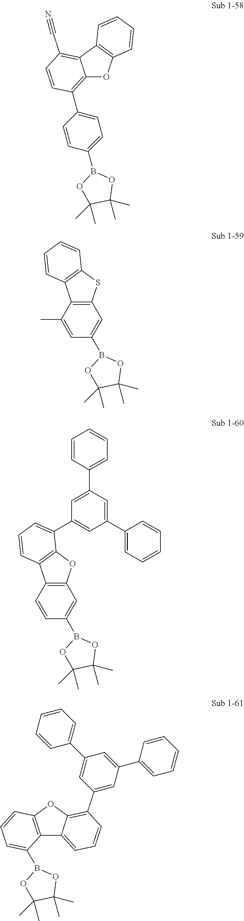


| TABLE 1 | |||
| Compound | FD-MS | Compound | FD-MS |
| Sub 1-1 | m/z = 294.14(C18H19BO3 = 294.15) | Sub 1-2 | m/z = 310.12(C18H19BO2S = 310.22) |
| Sub 1-3 | m/z = 370.17(C24H23BO3 = 370.25) | Sub 1-4 | m/z = 386.15(C24H23BO2S = 386.31) |
| Sub 1-5 | m/z = 420.19(C28H25BO3 = 420.31) | Sub 1-6 | m/z = 462.18(C30H27BO2S = 462.41) |
| Sub 1-7 | m/z = 370.17(C24H23BO3 = 370.25) | Sub 1-8 | m/z = 386.15(C24H23BO2S = 386.31) |
| Sub 1-9 | m/z = 294.14(C18H19BO3 = 294.15) | Sub 1-10 | m/z = 310.12(C18H19BO2S = 310.22) |
| Sub 1-11 | m/z = 370.17(C24H23BO3 = 370.25) | Sub 1-12 | m/z = 386.15(C24H23BO2S = 386.31) |
| Sub 1-13 | m/z = 294.14(C18H19BO3 = 294.15) | Sub 1-14 | m/z = 310.12(C18H19BO2S = 310.22) |
| Sub 1-15 | m/z = 386.15(C24H23BO2S = 386.31) | Sub 1-16 | m/z = 370.17(C24H23BO3 = 370.25) |
| Sub 1-17 | m/z = 344.16(C22H21BO3 = 344.21) | Sub 1-18 | m/z = 360.14(C22H21BO2S = 360.28) |
| Sub 1-19 | m/z = 420.19(C28H25BO3 = 420.31) | Sub 1-20 | m/z = 512.20(C34H29BO2S = 512.47) |
| Sub 1-21 | m/z = 344.16(C22H21BO3 = 344.21) | Sub 1-22 | m/z = 360.14(C22H21BO2S = 360.28) |
| Sub 1-23 | m/z = 436.17(C28H25BO2S = 436.37) | Sub 1-24 | m/z = 496.22(C34H29BO3 = 496.40) |
| Sub 1-25 | m/z = 410.15(C26H23BO2S = 410.34) | Sub 1-26 | m/z = 394.17(C28H23BO3 = 394.27) |
| Sub 1-27 | m/z = 486.18(C32H27BO2S = 486.43) | Sub 1-28 | m/z = 470.21(C32H27BO3 = 470.37) |
| Sub 1-29 | m/z = 344.16(C22H21BO3 = 344.21) | Sub 1-30 | m/z = 360.14(C22H21BO2S = 360.28) |
| Sub 1-31 | m/z = 420.19(C28H25BO3 = 420.31) | Sub 1-32 | m/z = 436.17(C28H25BO2S = 436.37) |
| Sub 1-33 | m/z = 360.14(C22H21BO2S = 360.28) | Sub 1-34 | m/z = 344.16(C22H21BO3 = 344.21) |
| Sub 1-35 | m/z = 552.23(C37H33BO2S = 552.53) | Sub 1-36 | m/z = 420.19(C28H25BO3 = 420.31) |
| Sub 1-37 | m/z = 394.17(C26H23BO3 = 394.27) | Sub 1-38 | m/z = 410.15(C26H23BO2S = 410.34) |
| Sub 1-39 | m/z = 576.19(C38H29BO3S = 576.51) | Sub 1-40 | m/z = 486.18(C32H27BO2S = 486.43) |
| Sub 1-41 | m/z = 344.16(C22H21BO3 = 344.21) | Sub 1-42 | m/z = 360.14(C22H21BO2S = 360.28) |
| Sub 1-43 | m/z = 476.16(C30H25BO3S = 476.39) | Sub 1-44 | m/z = 360.14(C22H21BO2S = 360.28) |
| Sub 1-45 | m/z = 344.16(C22H21BO3 = 344.21) | Sub 1-46 | m/z = 475.16(C30H25BO3S = 476.39) |
| Sub 1-47 | m/z = 410.15(C26H23BO2S = 410.34) | Sub 1-48 | m/z = 394.17(C28H23BO3 = 394.27) |
| Sub 1-49 | m/z = 486.18(C32H27BO2S = 486.43) | Sub 1-50 | m/z = 520.22(C35H29BO3 = 52.42) |
| Sub 1-51 | m/z = 360.14(C22H21BO2S = 360.28) | Sub 1-52 | m/z = 386.15(C24H23BO2S = 386.31) |
| Sub 1-53 | m/z = 436.17(C28H25BO2S = 436.37) | Sub 1-54 | m/z = 366.18(C22H27BO2S = 366.32) |
| Sub 1-55 | m/z = 470.21(C32H27BO3 = 470.37) | Sub 1-56 | m/z = 298.17(C18H15D4BO3 = 298.18) |
| Sub 1-57 | m/z = 414.20(C26H27BO4 = 414.30) | Sub 1-58 | m/z = 395.17(C25H22BNO3 = 395.26) |
| Sub 1-59 | m/z = 324.14(C19H21BO2S = 324.24) | Sub 1-60 | m/z = 522.24(C36H31BO3 = 522.44) |
| Sub 1-61 | m/z = 522.24(C36H31BO3 = 522.44) | Sub 1-62 | m/z = 386.15(C24H23BO2S = 386.31) |
| Sub 1-63 | m/z = 463.18(C29H26BNO2S = 463.40) | Sub 1-64 | m/z = 462.18(C30H27BO2S = 462.41) |
| Sub 1-65 | m/z = 471.20(C31H16BNO3 = 471.35) | Sub 1-66 | m/z = 436.17(C28H25BO2S = 436.37) |
| Sub 1-67 | m/z = 435.15(C27H22BNO2S = 435.35) | Sub 1-68 | m/z = 440.16(C27H25BO3S = 440.36) |
| Sub 1-69 | m/z = 511.18(C33H26BNO2S = 511.44) | ||


| TABLE 2 | |||
| Compound | FD-MS | Compound | FD-MS |
| Sub 2-1 | m/z = 490.10(C30H23BrN2 = 491.42) | Sub 2-2 | m/z = 794.23(C54H39BrN2 = 795.80) |
| Sub 2-3 | m/z = 690.17(C46H31BrN2 = 691.66) | Sub 2-4 | m/z = 822.26(C56H43BrN2 = 823.86) |
| Sub 2-5 | m/z = 970.29(C68H47BrN2 = 972.02) | Sub 2-6 | m/z = 742.20(C50H35BrN2 = 743.73) |
| Sub 2-7 | m/z = 742.20(C50H35BrN2 = 743.73) | Sub 2-8 | m/z = 616.15(C40H29BrN2 = 617.58) |
| Sub 2-9 | m/z = 702.08(C42H27BrN2S2 = 703.71) | Sub 2-10 | m/z = 670.13(C42H27BrN2O2 = 671.58) |
| Sub 2-11 | m/z = 742.20(C50H35BrN2 = 743.73) | Sub 2-12 | m/z = 809.25(C55H32D5BrN2 = 810.83) |
| Sub 2-13 | m/z = 690.17(C46H31BrN2 = 691.66) | Sub 2-14 | m/z = 566.14(C36H27BrN2 = 567.52) |
| Sub 2-15 | m/z = 746.14(C48H31BrN2S = 747.74) | Sub 2-16 | m/z = 600.20(C33H17D10BrN2 = 601.60) |
| Sub 2-17 | m/z = 642.17(C42H31BrN2 = 643.61) | Sub 2-18 | m/z = 778.11(C48H31BrN2S2 = 779.81) |
| Sub 2-19 | m/z = 670.13(C42H27BrN2O2 = 671.58) | Sub 2-20 | m/z = 590.14(C38H27BrN2 = 591.54) |
| Sub 2-21 | m/z = 540.12(C34H25BrN = 541.48) | Sub 2-22 | m/z = 590.14(C38H27BrN2 = 591.54) |
| Sub 2-23 | m/z = 744.19(C48H33BrN4 = 745.71) | Sub 2-24 | m/z = 672.12(C42H29BrN2S = 673.66) |
| Sub 2-25 | m/z = 567.13(C35H26BrN3 = 568.51) | Sub 2-26 | m/z = 854.14(C54H35BrN2S2 = 855.90) |
| Sub 2-27 | m/z = 642.17(C42H31BrN2 = 643.63) | Sub 2-28 | m/z = 744.21(C50H37BrN2 = 745.75) |
| Sub 2-29 | m/z = 914.06(C54H31BrN2S4 = 916.00) | Sub 2-30 | m/z = 540.12(C34H25BrN2 = 541.48) |
| Sub 2-31 | m/z = 600.20(C38H17D10BrN2 = 601.60) | Sub 2-32 | m/z = 728.18(C49H33BrN2 = 729.70) |
| Sub 2-33 | m/z = 796.22(C52H37BrN4 = 797.78) | Sub 2-34 | m/z = 742.20(C50H35BrN2 = 743.73) |
| Sub 2-35 | m/z = 566.14(C36H27BrN3 = 567.52) | Sub 2-36 | m/z = 682.20(C45H35BrN2 = 683.68) |
| Sub 2-37 | m/z = 518.14(C32H27BrN2 = 519.47) | Sub 2-38 | m/z = 616.15(C40H29BrN2 = 617.58) |
| Sub 2-39 | m/z = 492.09(C28H21BrN4 = 493.40) | Sub 2-40 | m/z = 758.23(C51H39BrN2 = 759.77) |
| Sub 2-41 | m/z = 606.17(C38H31BrN2 = 607.58) | Sub 2-42 | m/z = 614.14(C40H27BrN2 = 615.56) |
| Sub 2-43 | m/z = 541.12(C33H24BrN3 = 542.47) | Sub 2-44 | m/z = 690.17(C46H31BrN2 = 691.66) |
| Sub 2-45 | m/z = 794.23(C54H39BrN2 = 795.80) | Sub 2-46 | m/z = 672.12(C42H29BrN2S = 673.66) |
| Sub 2-47 | m/z = 690.17(C46H31BrN2 = 691.66) | Sub 2-48 | m/z = 670.20(C44H35BrN2 = 671.67) |
| Sub 2-49 | m/z = 686.10(C42H27BrN2OS = 687.65) | Sub 2-50 | m/z = 748.19(C48H37BrN2Si = 749.81) |
| Sub 2-51 | m/z = 690.17(C46H31BrN2 = 691.66) | Sub 2-52 | m/z = 954.35(C66H55BrN2 = 956.06) |
| Sub 2-53 | m/z = 780.21 (C53H37BrN2 = 781.78) | Sub 2-54 | m/z = 642.17(C42H31BrN2 = 643.61) |
| Sub 2-55 | m/z = 617.15(C39H28BrN3 = 618.56) | Sub 2-56 | m/z = 794.23(C54H39BrN2 = 795.80) |
| Sub 2-57 | m/z = 610.15(C34H31BrN2O4 = 611.52) | Sub 2-58 | m/z = 518.14(C32H27BrN2 = 519.47) |
| Sub 2-59 | m/z = 642.17(C42H31BrN2 = 643.61) | Sub 2-60 | m/z = 698.14(C44H31BrN2S = 699.70) |
| Sub 2-61 | m/z = 492.09(C28H21BrN4 = 493.40) | Sub 2-62 | m/z = 742.20(C50H35BrN2 = 743.73) |
| Sub 2-63 | m/z = 722.23(C48H39BrN2 = 723.74) | Sub 2-64 | m/z = 697.21(C46H28D5BrN2 = 698.70) |
| Sub 2-65 | m/z = 542.14(C34H27BrN2 = 543.50) | Sub 2-66 | m/z = 846.26(C58H43BrN2 = 847.88) |
| Sub 2-67 | m/z = 550.13(C32H27BrN2O2 = 551.47) | Sub 2-68 | m/z = 736.21(C48H37BrN2O = 737.72) |
| Sub 2-69 | m/z = 590.14(C38H27BrN2 = 591.54) | Sub 2-70 | m/z = 786.19(C51H35BrN2O2 = 787.74) |
| Sub 2-71 | m/z = 742.20(C50H35BrN2 = 743.73) | Sub 2-72 | m/z = 642.17(C42H31BrN2 = 643.61) |
| Sub 2-73 | m/z = 596.09(C36H25BrN2S = 597.57) | Sub 2-74 | m/z = 672.12(C42H29BrN2S = 673.66) |
| Sub 2-75 | m/z = 702.08(C42H27BrN2S2 = 703.71) | Sub 2-76 | m/z = 702.08(C42H27BrN2S2 = 703.71) |
| Sub 2-77 | m/z = 761.15(C48H32BrN3S = 762.76) | Sub 2-78 | m/z = 820.22(C54H37BrN4 = 821.80) |
| Sub 2-79 | m/z = 655.16(C42H30BrN3 = 656.61) | Sub 2-80 | m/z = 731.19(C48H34BrN3 = 732.71) |
| Sub 2-81 | m/z = 781.21(C52H35BrN3 = 782.77) | Sub 2-82 | m/z = 745.17(C48H32BrN3O = 746.69) |
| Sub 2-83 | m/z = 732.18(C48H33BrN2O = 733.69) | Sub 2-84 | m/z = 706.16(C46H31BrN2O = 707.66) |
| Sub 2-85 | m/z = 802.11(C50H31BrN2S2 = 803.83) | Sub 2-86 | m/z = 772.21(C51H37BrN2O = 773.76) |
| Sub 2-87 | m/z = 838.17(C54H35BrN2OS = 839.84) | Sub 2-88 | m/z = 807.22(C54H38BrN3 = 808.80) |
| Sub 2-89 | m/z = 778.20(C53H35BrN2 = 779.76) | Sub 2-90 | m/z = 811.17(C52H34BrN3S = 812.82) |
| Sub 2-91 | m/z = 646.20(C42H35BrN2 = 647.64) | Sub 2-92 | m/z = 747.23(C50H30D5BrN2 = 748.76) |
| Sub 2-93 | m/z = 688.21(C44H37BrN2O = 689.68) | Sub 2-94 | m/z = 646.20(C42H35BrN2 = 647.64) |
| Sub 2-95 | m/z = 796.15(C52H33BrN2S = 797.80) | Sub 2-96 | m/z = 673.17(C42H32BrN3O = 674.63) |
| Sub 2-97 | m/z = 762.20(C50H35BrFN2 = 763.74) | Sub 2-98 | m/z = 758.23(C51H39BrN2 = 759.77) |
| Sub 2-99 | m/z = 788.24(C46H45BrN4Si2 = 789.95) | Sub 2-100 | m/z = 712.21(C46H37BrN2O = 713.70) |
| Sub 2-101 | m/z = 742.20(C50H35BrN2 = 743.73) | Sub 2-102 | m/z = 754.11(C46H31BrN2S2 = 755.79) |
| Sub 2-103 | m/z = 667.16(C43H30BrN3 = 668.62) | Sub 2-104 | m/z = 656.15(C42H29BrN2O = 657.60) |
| Sub 2-105 | m/z = 994.29(C70H47BrN2 = 996.04) | Sub 2-106 | m/z = 738.17(C50H31BrN2 = 739.70) |
| Sub 2-107 | m/z = 762.22(C50H39BrN2O = 763.76) | ||


| TABLE 3 | |||
| Compound | FD-MS | Compound | FD-MS |
| P-1 | m/z = 578.24(C42H30N2O = 578.70) | P-2 | m/z = 882.36(C66H46N2O = 883.08) |
| P-3 | m/z = 794.28(C58H38N2S = 795.00) | P-4 | m/z = 926.37(C68H50N2S = 927.20) |
| P-5 | m/z = 1134.45(C86H58N2O = 1135.39) | P-6 | m/z = 906.36(C68H46N2O = 907.11) |
| P-7 | m/z = 922.34(C68H46N2S = 923.17) | P-8 | m/z = 796.29(C58H40N2S = 797.02) |
| P-9 | m/z = 916.26(C64H40N2OS2 = 917.15) | P-10 | m/z = 926.30(C66H42N2O2S = 927.12) |
| P-11 | m/z = 906.36(C58H46N2O = 907.11) | P-12 | m/z = 989.39(C73H43D5N2S = 990.27) |
| P-13 | m/z = 778.30(C58H38N2O = 778.94) | P-14 | m/z = 654.27(C48H34N2O = 654.80) |
| P-15 | m/z = 850.25(C50H38N2S2 = 851.09) | P-16 | m/z = 704.31(C50H24D10N2S = 704.94) |
| P-17 | m/z = 746.28(C54H38N2S = 746.96) | P-18 | m/z = 866.24(C60H38N2OS2 = 867.09) |
| P-19 | m/z = 834.29(C60H38N2O3 = 834.96) | P-20 | m/z = 770.28(C55H38N2S = 770.98) |
| P-21 | m/z = 628.25(C46H32N2O = 628.76) | P-22 | m/z = 694.24(C50H34N2S = 694.88) |
| P-23 | m/z = 848.30(C50H40N4S = 849.05) | P-24 | m/z = 760.25(C54H36N2OS = 760.94) |
| P-25 | m/z = 671.24(C47H33N3S = 671.85) | P-26 | m/z = 942.27(C66H42N2OS2 = 943.18) |
| P-27 | m/z = 822.31(C60H42N2S = 823.05) | P-28 | m/z = 908.38(C68H48N2O = 909.12) |
| P-29 | m/z = 1052.20(C70H40N2OS4 = 1053.34) | P-30 | m/z = 694.24(C50H34N2S = 694.88) |
| P-31 | m/z = 814.38(C50H30D10N2O = 815.03) | P-32 | m/z = 1034.37(C77H50N2S = 1035.30) |
| P-33 | m/z = 934.37(C68H46N4O = 935.12) | P-34 | m/z = 896.32(C66H44N2S = 897.13) |
| P-35 | m/z = 796.29(C58H40N2S = 797.02) | P-36 | m/z = 972.41(C73H52N3O = 973.21) |
| P-37 | m/z = 722.28(C52H38N2S = 722.94) | P-38 | m/z = 804.31(C60H40N2O = 804.97) |
| P-39 | m/z = 772.27(C54H36N4S = 772.96) | P-40 | m/z = 1022.42(C77H54N2O = 1023.27) |
| P-41 | m/z = 744.31(C55H43N2O = 744.92) | P-42 | m/z = 768.26(C56H36N2S = 768.96) |
| P-43 | m/z = 755.29(C55H37N3O = 755.90) | p-44 | m/z = 920.32(C68H44N2S = 921.16) |
| P-45 | m/z = 948.35(C70H48N2S = 949.21) | P-46 | m/z = 810.27(C58H38N2OS = 811.00) |
| P-47 | m/z = 1036.39(C77H52N2S = 1037.32) | P-48 | m/z = 884.38(C66H48N2O = 885.10) |
| P-49 | m/z = 874.27(C62H38N2O2S = 875.04) | P-50 | m/z = 952.33(C68H48N2SSi = 953.27) |
| P-51 | m/z = 1060.35(C78H48N2OS = 1061.29) | P-52 | m/z = 1234.53(C92H70N2S = 1235.62) |
| P-53 | m/z = 918.36(C69H46N2O = 919.12) | P-54 | m/z = 79629(C58H40N2S = 797.02) |
| P-55 | m/z = 887.30(C63H41N3OS = 888.08) | P-56 | m/z = 948.35(C70H48N2S = 949.21 ) |
| P-57 | m/z = 764.27(C50H40N2O4S = 764.93) | P-58 | m/z = 656.28(C48H36N2O = 656.81 ) |
| P-59 | m/z = 912.32(C66H44N2OS = 913.13) | P-60 | m/z = 836.29(C60H40N2OS = 837.04) |
| P-61 | m/z = 696.23(C48H32N4S = 696.86) | P-62 | m/z = 930.36(C70H46N2O = 931.13) |
| P-63 | m/z = 1002.40(C74H54N2S = 1003.30) | P-64 | m/z = 1011.42(C76H45D5N2O = 1012.25) |
| P-65 | m/z = 630.27(C46H34N2O = 630.77) | P-66 | m/z = 934.39(C70H50N2O = 935.16) |
| P-67 | m/z = 704.25(C48H36N2O2S = 704.88) | P-68 | m/z = 840.32(C60H44N2OS = 841.07) |
| P-69 | m/z = 820.29(C60H40N2S = 821.04) | P-70 | m/z = 966.33(C69H46N2O2S = 967.18) |
| P-71 | m/z = 694.24(C50H34N2S = 694.88) | P-72 | m/z = 846.31(C62H42N2S = 847.08) |
| P-73 | m/z = 746.28(C54H38N2S = 746.96) | P-74 | m/z = 898.34(C66H46N2S = 899.15) |
| P-75 | m/z = 700.20(C48H32N2S2 = 700.91) | P-76 | m/z = 776.23(C54H36N2S2 = 777.01) |
| P-77 | m/z = 776.23(C54H36N2S2 = 777.01) | P-78 | m/z = 806.19(C54H34N2S3 = 807.06) |
| P-79 | m/z = 806.19(C54H34N2S3 = 807.06) | P-80 | m/z = 806.19(C54H34N2S3 = 807.06) |
| P-81 | m/z = 865.26(C50H39N3S2 = 866.10) | P-82 | m/z = 924.33(C66H44N4S = 925.15) |
| P-83 | m/z = 759.27(C54H37N3S = 759.96) | P-84 | m/z = 835.30(C60H41N3S = 836.05) |
| P-85 | m/z = 935.33(C68H45N3S = 936.17) | P-86 | m/z = 899.30(C64H41N3OS = 900.09) |
| P-87 | m/z = 886.30(C64H42N2OS = 887.10) | P-88 | m/z = 860.29(C62H40N2OS = 861.06) |
| P-89 | m/z = 730.30(C54H38N2O = 730.89) | P-90 | m/z = 760.25(C54H36N2OS = 760.94) |
| P-91 | m/z = 890.24(C62H38N2OS2 = 891.11) | P-92 | m/z = 860.34(C63H44N2O2 = 861.04) |
| P-93 | m/z = 926.30(C66H42N2O2S = 927.12) | P-94 | m/z = 895.36(C66H45N3O = 896.08) |
| P-95 | m/z = 866.33(C65H42N2O = 867.04) | P-96 | m/z = 949.31(C68H43N3OS = 950.15) |
| P-97 | m/z = 754.30(C56H38N2O = 754.91) | P-98 | m/z = 886.39(C66H42D4N2O = 887.11) |
| P-99 | m/z = 850.34(C62H46N2S = 851.11) | P-100 | m/z = 826.34(C60H46N2S = 827.09) |
| P-101 | m/z = 1178.48(C88H62N2O2 = 1179.45) | P-102 | m/z = 931.36(C69H45N3O = 932.12) |
| P-103 | m/z = 927.37(C68H41D5N2S = 928.20) | P-104 | m/z = 868.35(C62H48N2OS = 869.12) |
| P-105 | m/z = 1006.39(C76H50N2O = 1007.22) | P-106 | m/z = 734.33(C54H42N2O = 734.92) |
| P-107 | m/z = 900.26(C64H40N2S2 = 901.15) | P-108 | m/z = 718.32(C51H26D10N2S = 718.97) |
| P-109 | m/z = 930.34(C65H46N4OS = 931.15) | P-110 | m/z = 1170.37(C84H54N2OS2 = 1171.47) |
| P-111 | m/z = 898.34(C66H46N2S = 899.15) | P-112 | m/z = 926.37(C68H47FN2O = 927.11) |
| P-113 | m/z = 780.31(C58H40N2O = 780.95) | P-114 | m/z = 1064.42(C79H56N2S = 1065.37) |
| P-115 | m/z = 899.37(C61H53N3OSi2 = 900.26) | P-116 | m/z = 942.36(C68H50N2OS = 943.20) |
| P-117 | m/z = 747.27(C53H37N3S = 747.95) | P-118 | m/z = 930.36(C70H46N2O = 931.13) |
| P-119 | m/z = 942.27(C66H42N2OS2 = 943.18) | P-120 | m/z = 901.31(C64H43N3OS = 902.11) |
| P-121 | m/z = 860.29(C62H40N2OS = 861.06) | P-122 | m/z = 1182.45(C90H58N2O = 1183.44) |
| P-123 | m/z = 1043.33(C77H45N3S = 1044.27) | P-124 | m/z = 1076.43(C80H56N2O2 = 1077.31) |


| TABLE 4 | |||||||
| Current | |||||||
| Voltage | Density | Brightness | Efficiency | Lifetime | CIE | ||
| compound | (V) | (mA/cm2) | (cd/m2) | (cd/A) | T(95) | x | y | ||
| comp. Ex (I-1) | comp. Com 1 | 6.0 | 21.5 | 5000 | 23.3 | 57.2 | 0.32 | 0.61 |
| comp. Ex (I-2) | comp. Com 2 | 5.9 | 18.2 | 5000 | 27.5 | 74.5 | 0.32 | 0.62 |
| comp. Ex (I-3) | comp. Com 3 | 5.8 | 17.3 | 5000 | 29.0 | 78.6 | 0.33 | 0.61 |
| comp. Ex (I-4) | comp. Com 4 | 5.8 | 17.9 | 5000 | 27.9 | 76.5 | 0.33 | 0.62 |
| comp. Ex (I-5) | comp. Com 5 | 5.8 | 16.8 | 5000 | 29.8 | 79.2 | 0.33 | 0.61 |
| Ex. (I-1) | Com. (P-1) | 5.7 | 14.0 | 5000 | 35.8 | 130.2 | 0.33 | 0.61 |
| Ex. (I-2) | Com. (P-2) | 5.5 | 13.9 | 5000 | 36.1 | 130.5 | 0.33 | 0.61 |
| Ex. (I-3) | Com. (P-3) | 5.7 | 14.2 | 5000 | 35.1 | 124.0 | 0.33 | 0.61 |
| Ex. (I-4) | Com. (P-4) | 5.6 | 13.8 | 5000 | 36.3 | 125.9 | 0.33 | 0.62 |
| Ex. (I-5) | Com. (P-5) | 5.7 | 14.3 | 5000 | 35.0 | 131.1 | 0.33 | 0.62 |
| Ex. (I-6) | Com. (P-6) | 5.7 | 14.0 | 5000 | 35.8 | 130.5 | 0.33 | 0.61 |
| Ex. (I-7) | Com. (P-7) | 5.7 | 14.0 | 5000 | 35.6 | 131.2 | 0.33 | 0.61 |
| Ex. (I-8) | Com. (P-8) | 5.6 | 14.0 | 5000 | 35.6 | 130.6 | 0.33 | 0.61 |
| Ex. (I-9) | Com. (P-11) | 5.7 | 14.9 | 5000 | 33.6 | 120.8 | 0.33 | 0.62 |
| Ex. (I-10) | Com. (P-12) | 5.7 | 14.3 | 5000 | 34.9 | 112.6 | 0.33 | 0.61 |
| Ex. (I-11) | Com. (P-13) | 5.6 | 12.9 | 5000 | 38.7 | 142.8 | 0.33 | 0.62 |
| Ex. (I-12) | Com. (P-14) | 5.5 | 13.4 | 5000 | 37.4 | 137.1 | 0.33 | 0.61 |
| Ex. (I-13) | Com. (P-16) | 5.6 | 13.5 | 5000 | 37.0 | 124.7 | 0.33 | 0.61 |
| Ex. (I-14) | Com. (P-17) | 5.6 | 13.1 | 5000 | 38.3 | 138.1 | 0.33 | 0.62 |
| Ex. (I-15) | Com. (P-18) | 5.7 | 14.0 | 5000 | 35.6 | 129.9 | 0.33 | 0.61 |
| Ex. (I-16) | Com. (P-19) | 5.5 | 12.8 | 5000 | 39.2 | 136.2 | 0.33 | 0.62 |
| Ex. (I-17) | Com. (P-20) | 5.5 | 13.7 | 5000 | 36.6 | 123.3 | 0.33 | 0.62 |
| Ex. (I-18) | Com. (P-21) | 5.7 | 14.2 | 5000 | 35.3 | 129.1 | 0.33 | 0.61 |
| Ex. (I-19) | Com. (P-22) | 5.7 | 14.1 | 5000 | 35.5 | 121.3 | 0.33 | 0.62 |
| Ex. (I-20) | Com. (P-24) | 5.7 | 14.5 | 5000 | 34.6 | 119.3 | 0.33 | 0.62 |
| Ex. (I-21) | Com. (P-27) | 5.7 | 14.2 | 5000 | 35.2 | 131.2 | 0.33 | 0.62 |
| Ex. (I-22) | Com. (P-28) | 5.6 | 14.6 | 5000 | 34.3 | 114.5 | 0.33 | 0.62 |
| Ex. (I-23) | Com. (P-30) | 5.7 | 16.1 | 5000 | 31.0 | 112.9 | 0.33 | 0.62 |
| Ex. (I-24) | Com. (P-31) | 5.7 | 15.9 | 5000 | 31.4 | 116.8 | 0.33 | 0.62 |
| Ex. (I-25) | Com. (P-32) | 5.7 | 16.4 | 5000 | 30.6 | 108.4 | 0.33 | 0.61 |
| Ex. (I-26) | Com. (P-34) | 5.7 | 16.1 | 5000 | 31.1 | 108.5 | 0.33 | 0.61 |
| Ex. (I-27) | Com. (P-35) | 5.6 | 16.1 | 5000 | 31.0 | 114.4 | 0.33 | 0.61 |
| Ex. (I-28) | Com. (P-36) | 5.7 | 16.2 | 5000 | 30.9 | 106.8 | 0.33 | 0.61 |
| Ex. (I-29) | Com. (P-37) | 5.7 | 16.3 | 5000 | 30.7 | 108.2 | 0.33 | 0.61 |
| Ex. (I-30) | Com. (P-38) | 5.7 | 16.1 | 5000 | 31.0 | 114.9 | 0.33 | 0.61 |
| Ex. (I-31) | Com. (P-40) | 5.7 | 16.1 | 5000 | 31.0 | 115.3 | 0.33 | 0.62 |
| Ex. (I-32) | Com. (P-41) | 5.7 | 14.7 | 5000 | 34.1 | 121.2 | 0.33 | 0.61 |
| Ex. (I-33) | Com. (P-42) | 5.7 | 15.1 | 5000 | 33.2 | 110.6 | 0.33 | 0.61 |
| Ex. (I-34) | Com. (P-44) | 5.7 | 15.3 | 5000 | 32.7 | 113.6 | 0.33 | 0.61 |
| Ex. (I-35) | Com. (P-45) | 5.7 | 14.9 | 5000 | 33.6 | 114.3 | 0.33 | 0.61 |
| Ex. (I-36) | Com. (P-46) | 5.6 | 15.1 | 5000 | 33.2 | 119.7 | 0.33 | 0.61 |
| Ex. (I-37) | Com. (P-47) | 5.6 | 15.5 | 5000 | 32.2 | 112.8 | 0.33 | 0.62 |
| Ex. (I-38) | Com. (P-51) | 5.6 | 15.6 | 5000 | 32.1 | 120.9 | 0.33 | 0.62 |
| Ex. (I-39) | Com. (P-53) | 5.6 | 15.7 | 5000 | 31.8 | 114.1 | 0.33 | 0.61 |
| Ex. (I-40) | Com. (P-56) | 5.7 | 16.3 | 5000 | 30.7 | 114.2 | 0.33 | 0.61 |
| Ex. (I-41) | Com. (P-60) | 5.7 | 16.3 | 5000 | 30.6 | 115.5 | 0.33 | 0.62 |
| Ex. (I-42) | Com. (P-62) | 5.6 | 16.1 | 5000 | 31.0 | 116.8 | 0.33 | 0.61 |
| Ex. (I-43) | Com. (P-63) | 5.6 | 16.3 | 5000 | 30.6 | 110.4 | 0.33 | 0.61 |
| Ex. (I-44) | Com. (P-69) | 5.7 | 14.9 | 5000 | 33.4 | 116.7 | 0.33 | 0.62 |
| Ex. (I-45) | Com. (P-71) | 5.6 | 13.5 | 5000 | 37.1 | 130.7 | 0.33 | 0.61 |
| Ex. (I-46) | Com. (P-72) | 5.5 | 13.2 | 5000 | 37.9 | 133.0 | 0.33 | 0.62 |
| Ex. (I-47) | Com. (P-73) | 5.6 | 12.9 | 5000 | 38.6 | 138.1 | 0.33 | 0.61 |
| Ex. (I-48) | Com. (P-74) | 5.5 | 13.1 | 5000 | 38.1 | 134.5 | 0.33 | 0.62 |
| Ex. (I-49) | Com. (P-75) | 5.5 | 13.6 | 5000 | 36.8 | 125.7 | 0.33 | 0.62 |
| Ex. (I-50) | Com. (P-82) | 5.5 | 13.8 | 5000 | 36.1 | 126.3 | 0.33 | 0.62 |
| Ex. (I-51) | Com. (P-83) | 5.5 | 13.2 | 5000 | 37.8 | 134.0 | 0.33 | 0.61 |
| Ex. (I-52) | Com. (P-84) | 5.6 | 13.3 | 5000 | 37.7 | 130.6 | 0.33 | 0.62 |
| Ex. (I-53) | Com. (P-85) | 5.6 | 14.5 | 5000 | 34.4 | 114.2 | 0.33 | 0.62 |
| Ex. (I-54) | Com. (P-89) | 5.5 | 13.0 | 5000 | 38.5 | 142.9 | 0.33 | 0.62 |
| Ex. (I-55) | Com. (P-90) | 5.6 | 13.7 | 5000 | 36.5 | 130.2 | 0.33 | 0.62 |
| Ex. (I-56) | Com. (P-94) | 5.7 | 14.3 | 5000 | 35.1 | 130.5 | 0.33 | 0.62 |
| Ex. (I-57) | Com. (P-95) | 5.5 | 13.2 | 5000 | 37.8 | 136.1 | 0.33 | 0.62 |
| Ex. (I-58) | Com. (P-96) | 5.6 | 14.3 | 5000 | 35.1 | 130.1 | 0.33 | 0.62 |

| TABLE 5 | |||||||
| Current | |||||||
| Voltage | Density | Brightness | Efficiency | Lifetime | CIE | ||
| compound | (V) | (mA/cm2) | (cd/m2) | (cd/A) | T(95) | x | y | ||
| comp. Ex (II-1) | — | 6.0 | 21.5 | 5000 | 23.3 | 57.2 | 0.32 | 0.61 |
| comp. Ex (II-2) | comp. Com 4 | 6.4 | 13.6 | 5000 | 36.6 | 101.4 | 0.33 | 0.61 |
| comp. Ex (II-3) | comp. Com 5 | 6.5 | 13.5 | 5000 | 37.0 | 100.9 | 0.33 | 0.61 |
| comp. Ex (II-4) | comp. Com 6 | 6.5 | 15.4 | 5000 | 32.4 | 91.8 | 0.33 | 0.61 |
| comp. Ex (II-5) | comp. Com 7 | 6.5 | 16.7 | 5000 | 30.0 | 88.9 | 0.33 | 0.61 |
| comp. Ex (II-6) | comp. Com 8 | 6.5 | 12.5 | 5000 | 40.0 | 105.8 | 0.33 | 0.61 |
| Ex. (II-1) | Com. (P-1) | 6.4 | 10.7 | 5000 | 46.7 | 144.6 | 0.33 | 0.61 |
| Ex. (II-2) | Com. (P-2) | 6.3 | 10.5 | 5000 | 47.7 | 147.6 | 0.33 | 0.61 |
| Ex. (II-3) | Com. (P-3) | 6.3 | 10.6 | 5000 | 47.0 | 157.0 | 0.33 | 0.61 |
| Ex. (II-4) | Com. (P-6) | 6.3 | 11.0 | 5000 | 45.3 | 142.4 | 0.33 | 0.61 |
| Ex. (II-5) | Com. (P-7) | 6.4 | 10.8 | 5000 | 46.3 | 144.2 | 0.33 | 0.61 |
| Ex. (II-6) | Com. (P-8) | 6.3 | 10.7 | 5000 | 46.6 | 144.7 | 0.33 | 0.61 |
| Ex. (II-7) | Com. (P-9) | 6.4 | 11.3 | 5000 | 44.3 | 142.2 | 0.33 | 0.61 |
| Ex. (II-8) | Com. (P-12) | 6.3 | 10.9 | 5000 | 46.0 | 146.9 | 0.33 | 0.61 |
| Ex. (II-9) | Com. (P-13) | 6.3 | 10.6 | 5000 | 47.3 | 152.9 | 0.33 | 0.61 |
| Ex. (II-10) | Com. (P-14) | 6.2 | 10.3 | 5000 | 48.4 | 158.8 | 0.33 | 0.61 |
| Ex. (II-11) | Com. (P-15) | 6.3 | 10.1 | 5000 | 49.6 | 170.5 | 0.33 | 0.61 |
| Ex. (II-12) | Com. (P-16) | 6.2 | 10.2 | 5000 | 49.2 | 164.2 | 0.33 | 0.61 |
| Ex. (II-13) | Com. (P-17) | 6.2 | 10.3 | 5000 | 48.7 | 155.2 | 0.33 | 0.61 |
| Ex. (II-14) | Com. (P-18) | 6.3 | 10.4 | 5000 | 48.0 | 164.2 | 0.33 | 0.62 |
| Ex. (II-15) | Com. (P-19) | 6.4 | 10.8 | 5000 | 46.5 | 145.1 | 0.33 | 0.62 |
| Ex. (II-16) | Com. (P-20) | 6.4 | 10.8 | 5000 | 46.4 | 143.6 | 0.33 | 0.62 |
| Ex. (II-17) | Com. (P-21) | 6.4 | 10.8 | 5000 | 46.1 | 144.9 | 0.33 | 0.62 |
| Ex. (II-18) | Com. (P-22) | 6.3 | 10.5 | 5000 | 47.8 | 154.8 | 0.33 | 0.62 |
| Ex. (II-19) | Com. (P-24) | 6.4 | 10.4 | 5000 | 48.2 | 150.9 | 0.33 | 0.62 |
| Ex. (II-20) | Com. (P-25) | 6.4 | 10.7 | 5000 | 46.8 | 157.3 | 0.33 | 0.61 |
| Ex. (II-21) | Com. (P-26) | 6.4 | 10.7 | 5000 | 46.7 | 140.5 | 0.33 | 0.61 |
| Ex. (II-22) | Com. (P-27) | 6.3 | 10.7 | 5000 | 46.6 | 147.3 | 0.33 | 0.61 |
| Ex. (II-23) | Com. (P-29) | 6.4 | 10.9 | 5000 | 45.9 | 141.4 | 0.33 | 0.61 |
| Ex. (II-24) | Com. (P-30) | 6.3 | 10.7 | 5000 | 46.9 | 148.5 | 0.33 | 0.62 |
| Ex. (II-25) | Com. (P-34) | 6.3 | 10.7 | 5000 | 46.7 | 152.8 | 0.33 | 0.62 |
| Ex. (II-26) | Com. (P-35) | 6.4 | 10.9 | 5000 | 45.7 | 145.4 | 0.33 | 0.62 |
| Ex. (II-27) | Com. (P-37) | 6.4 | 10.7 | 5000 | 46.6 | 151.8 | 0.33 | 0.61 |
| Ex. (II-28) | Com. (P-38) | 6.3 | 10.9 | 5000 | 45.9 | 143.7 | 0.33 | 0.62 |
| Ex. (II-29) | Com. (P-41) | 6.4 | 10.8 | 5000 | 46.5 | 154.5 | 0.33 | 0.61 |
| Ex. (II-30) | Com. (P-42) | 6.3 | 10.4 | 5000 | 48.1 | 153.1 | 0.33 | 0.61 |
| Ex. (II-31) | Com. (P-44) | 6.4 | 10.9 | 5000 | 46.0 | 140.8 | 0.33 | 0.61 |
| Ex. (II-32) | Com. (P-45) | 6.3 | 10.5 | 5000 | 47.8 | 157.2 | 0.33 | 0.62 |
| Ex. (II-33) | Com. (P-46) | 6.2 | 10.6 | 5000 | 47.1 | 153.9 | 0.33 | 0.62 |
| Ex. (II-34) | Com. (P-49) | 6.3 | 10.8 | 5000 | 46.5 | 157.2 | 0.33 | 0.61 |
| Ex. (II-35) | Com. (P-62) | 6.4 | 11.0 | 5000 | 45.6 | 146.3 | 0.33 | 0.61 |
| Ex. (II-36) | Com. (P-69) | 6.3 | 10.5 | 5000 | 47.4 | 148.0 | 0.33 | 0.62 |
| Ex. (II-37) | Com. (P-71) | 6.3 | 10.2 | 5000 | 49.1 | 155.8 | 0.33 | 0.62 |
| Ex. (II-38) | Com. (P-72) | 6.2 | 10.2 | 5000 | 48.8 | 161.4 | 0.33 | 0.62 |
| Ex. (II-39) | Com. (P-73) | 6.2 | 10.0 | 5000 | 50.1 | 171.6 | 0.33 | 0.61 |
| Ex. (II-40) | Com. (P-74) | 6.2 | 10.0 | 5000 | 50.0 | 170.5 | 0.33 | 0.62 |
| Ex. (II-41) | Com. (P-75) | 6.2 | 9.9 | 5000 | 50.6 | 173.3 | 0.33 | 0.62 |
| Ex. (II-42) | Com. (P-76) | 6.3 | 9.8 | 5000 | 51.0 | 173.3 | 0.33 | 0.61 |
| Ex. (II-43) | Com. (P-77) | 6.3 | 9.8 | 5000 | 51.0 | 174.1 | 0.33 | 0.62 |
| Ex. (II-44) | Com. (P-78) | 6.3 | 10.2 | 5000 | 49.2 | 157.6 | 0.33 | 0.62 |
| Ex. (II-45) | Com. (P-79) | 6.2 | 10.0 | 5000 | 49.9 | 167.2 | 0.33 | 0.61 |
| Ex. (II-46) | Com. (P-80) | 6.3 | 10.0 | 5000 | 50.1 | 168.1 | 0.33 | 0.61 |
| Ex. (II-47) | Com. (P-81) | 6.2 | 10.2 | 5000 | 49.2 | 171.3 | 0.33 | 0.62 |
| Ex. (II-48) | Com. (P-82) | 6.2 | 10.3 | 5000 | 48.7 | 157.8 | 0.33 | 0.62 |
| Ex. (II-49) | Com. (P-83) | 6.3 | 10.0 | 5000 | 50.0 | 170.0 | 0.33 | 0.61 |
| Ex. (II-50) | Com. (P-84) | 6.3 | 10.0 | 5000 | 49.9 | 170.9 | 0.33 | 0.62 |
| Ex. (II-51) | Com. (P-85) | 6.3 | 10.4 | 5000 | 48.0 | 151.9 | 0.33 | 0.62 |
| Ex. (II-52) | Com. (P-86) | 6.3 | 10.4 | 5000 | 47.9 | 156.9 | 0.33 | 0.62 |
| Ex. (II-53) | Com. (P-87) | 6.2 | 10.3 | 5000 | 48.4 | 159.5 | 0.33 | 0.61 |
| Ex. (II-54) | Com. (P-88) | 6.2 | 10.2 | 5000 | 49.1 | 156.5 | 0.33 | 0.62 |
| Ex. (II-55) | Com. (P-89) | 6.3 | 10.3 | 5000 | 48.4 | 162.6 | 0.33 | 0.61 |
| Ex. (II-56) | Com. (P-90) | 6.2 | 10.2 | 5000 | 48.9 | 167.0 | 0.33 | 0.62 |
| Ex. (II-57) | Com. (P-91) | 6.2 | 10.6 | 5000 | 47.2 | 152.4 | 0.33 | 0.61 |
| Ex. (II-58) | Com. (P-92) | 6.3 | 10.6 | 5000 | 47.2 | 155.2 | 0.33 | 0.61 |
| Ex. (II-59) | Com. (P-93) | 6.3 | 10.3 | 5000 | 48.6 | 164.1 | 0.33 | 0.62 |
| Ex. (II-60) | Com. (P-94) | 6.3 | 10.4 | 5000 | 48.2 | 164.8 | 0.33 | 0.62 |
| Ex. (II-61) | Com. (P-95) | 6.3 | 10.5 | 5000 | 47.5 | 157.4 | 0.33 | 0.62 |
| Ex. (II-62) | Com. (P-96) | 6.3 | 10.6 | 5000 | 47.2 | 153.7 | 0.33 | 0.62 |
| TABLE 6 | |||||||
| Current | |||||||
| Voltage | Density | Brightness | Efficiency | Lifetime | CIE | ||
| compound | (V) | (mA/cm2) | (cd/m2) | (cd/A) | T(95) | x | y | ||
| comp. Ex (III-1) | — | 6.5 | 33.8 | 2500 | 7.4 | 63.8 | 0.66 | 0.32 |
| comp. Ex (III-2) | comp. Com 4 | 6.9 | 25.4 | 2500 | 9.8 | 95.5 | 0.66 | 0.33 |
| comp. Ex (III-3) | comp. Com 5 | 6.8 | 25.3 | 2500 | 9.9 | 96.7 | 0.66 | 0.33 |
| comp. Ex (III-4) | comp. Com 6 | 6.9 | 26.6 | 2500 | 9.4 | 91.0 | 0.66 | 0.32 |
| comp. Ex (III-5) | comp. Com 7 | 6.9 | 27.7 | 2500 | 9.0 | 88.5 | 0.66 | 0.33 |
| comp. Ex (III-6) | comp. Com 8 | 6.8 | 23.0 | 2500 | 10.9 | 95.7 | 0.66 | 0.33 |
| Ex. (III-1) | Com. (P-1) | 6.7 | 20.7 | 2500 | 12.1 | 133.0 | 0.66 | 0.33 |
| Ex. (III-2) | Com. (P-2) | 6.7 | 19.9 | 2500 | 12.6 | 136.5 | 0.66 | 0.33 |
| Ex. (III-3) | Com. (P-3) | 6.7 | 18.4 | 2500 | 13.6 | 136.1 | 0.66 | 0.33 |
| Ex. (III-4) | Com. (P-6) | 6.8 | 20.8 | 2500 | 12.0 | 128.2 | 0.66 | 0.32 |
| Ex. (III-5) | Com. (P-14) | 6.8 | 18.4 | 2500 | 13.6 | 145.0 | 0.66 | 0.32 |
| Ex. (III-6) | Com. (P-15) | 6.7 | 15.8 | 2500 | 15.8 | 159.3 | 0.66 | 0.32 |
| Ex. (III-7) | Com. (P-16) | 6.6 | 17.0 | 2500 | 14.7 | 156.3 | 0.66 | 0.32 |
| Ex. (III-8) | Com. (P-17) | 6.6 | 17.3 | 2500 | 14.4 | 152.8 | 0.66 | 0.32 |
| Ex. (III-9) | Com. (P-18) | 6.7 | 16.8 | 2500 | 14.9 | 154.9 | 0.66 | 0.32 |
| Ex. (III-10) | Com. (P-19) | 6.7 | 20.2 | 2500 | 12.4 | 126.7 | 0.66 | 0.32 |
| Ex. (III-11) | Com. (P-20) | 6.7 | 20.4 | 2500 | 12.3 | 134.0 | 0.66 | 0.32 |
| Ex. (III-12) | Com. (P-21) | 6.8 | 20.4 | 2500 | 12.2 | 127.0 | 0.66 | 0.33 |
| Ex. (III-13) | Com. (P-22) | 6.8 | 19.1 | 2500 | 13.1 | 140.0 | 0.66 | 0.32 |
| Ex. (III-14) | Com. (P-24) | 6.8 | 17.7 | 2500 | 14.1 | 147.8 | 0.66 | 0.33 |
| Ex. (III-15) | Com. (P-30) | 6.8 | 19.6 | 2500 | 12.8 | 137.5 | 0.66 | 0.32 |
| Ex. (III-16) | Com. (P-31) | 6.8 | 21.2 | 2500 | 11.8 | 128.2 | 0.66 | 0.33 |
| Ex. (III-17) | Com. (P-34) | 6.7 | 19.9 | 2500 | 12.6 | 137.0 | 0.66 | 0.32 |
| Ex. (III-18) | Com. (P-45) | 6.7 | 17.4 | 2500 | 14.4 | 147.1 | 0.66 | 0.33 |
| Ex. (III-19) | Com. (P-46) | 6.8 | 18.6 | 2500 | 13.5 | 138.7 | 0.66 | 0.32 |
| Ex. (III-20) | Com. (P-49) | 6.7 | 18.3 | 2500 | 13.6 | 138.2 | 0.66 | 0.32 |
| Ex. (III-21) | Com. (P-69) | 6.8 | 18.0 | 2500 | 13.9 | 139.2 | 0.66 | 0.32 |
| Ex. (III-22) | Com. (P-70) | 6.7 | 19.2 | 2500 | 13.0 | 142.4 | 0.66 | 0.32 |
| Ex. (III-23) | Com. (P-71) | 6.6 | 17.3 | 2500 | 14.4 | 151.6 | 0.66 | 0.33 |
| Ex. (III-24) | Com. (P-72) | 6.6 | 17.2 | 2500 | 14.5 | 152.2 | 0.66 | 0.32 |
| Ex. (III-25) | Com. (P-73) | 6.7 | 17.1 | 2500 | 14.6 | 150.5 | 0.66 | 0.33 |
| Ex. (III-26) | Com. (P-74) | 6.6 | 17.1 | 2500 | 14.6 | 155.2 | 0.66 | 0.32 |
| Ex. (III-27) | Com. (P-75) | 6.6 | 15.5 | 2500 | 16.1 | 165.4 | 0.66 | 0.32 |
| Ex. (III-28) | Com. (P-76) | 6.6 | 14.8 | 2500 | 16.9 | 169.7 | 0.66 | 0.32 |
| Ex. (III-29) | Com. (P-77) | 6.6 | 15.2 | 2500 | 16.5 | 168.8 | 0.66 | 0.32 |
| Ex. (III-30) | Com. (P-78) | 6.6 | 16.6 | 2500 | 15.1 | 156.9 | 0.66 | 0.32 |
| Ex. (III-31) | Com. (P-79) | 6.6 | 15.8 | 2500 | 15.8 | 157.0 | 0.66 | 0.32 |
| Ex. (III-32) | Com. (P-80) | 6.6 | 15.9 | 2500 | 15.7 | 163.1 | 0.66 | 0.33 |
| Ex. (III-33) | Com. (P-81) | 6.7 | 15.8 | 2500 | 15.8 | 160.6 | 0.66 | 0.32 |
| Ex. (III-34) | Com. (P-82) | 6.6 | 16.4 | 2500 | 15.2 | 151.2 | 0.66 | 0.32 |
| Ex. (III-35) | Com. (P-83) | 6.7 | 15.9 | 2500 | 15.7 | 161.8 | 0.66 | 0.33 |
| Ex. (III-36) | Com. (P-84) | 6.7 | 16.1 | 2500 | 15.5 | 159.0 | 0.66 | 0.32 |
| Ex. (III-37) | Com. (P-85) | 6.8 | 17.7 | 2500 | 14.1 | 148.9 | 0.66 | 0.33 |
| Ex. (III-38) | Com. (P-86) | 6.8 | 17.4 | 2500 | 14.3 | 144.0 | 0.66 | 0.32 |
| Ex. (III-39) | Com. (P-87) | 6.7 | 16.9 | 2500 | 14.8 | 152.3 | 0.66 | 0.33 |
| Ex. (III-40) | Com. (P-88) | 6.6 | 16.8 | 2500 | 14.9 | 149.3 | 0.66 | 0.33 |
| Ex. (III-41) | Com. (P-89) | 6.7 | 18.0 | 2500 | 13.9 | 146.1 | 0.66 | 0.33 |
| Ex. (III-42) | Com. (P-90) | 6.6 | 16.5 | 2500 | 15.2 | 151.8 | 0.66 | 0.32 |
| Ex. (III-43) | Com. (P-91) | 6.8 | 17.6 | 2500 | 14.2 | 144.3 | 0.66 | 0.32 |
| Ex. (III-44) | Com. (P-92) | 6.8 | 17.5 | 2500 | 14.3 | 145.5 | 0.66 | 0.32 |
| Ex. (III-45) | Com. (P-93) | 6.6 | 17.1 | 2500 | 14.6 | 151.2 | 0.66 | 0.33 |
| Ex. (III-46) | Com. (P-94) | 6.6 | 16.7 | 2500 | 15.0 | 150.5 | 0.66 | 0.32 |
| Ex. (III-47) | Com. (P-95) | 6.7 | 18.1 | 2500 | 13.8 | 142.2 | 0.66 | 0.33 |
| Ex. (III-48) | Com. (P-96) | 6.8 | 17.8 | 2500 | 14.0 | 147.5 | 0.66 | 0.33 |
Claims (10)


Applications Claiming Priority (3)
| Application Number | Priority Date | Filing Date | Title |
|---|---|---|---|
| KR10-2015-0036231 | 2015-03-16 | ||
| KR1020150036231A KR101822477B1 (en) | 2015-03-16 | 2015-03-16 | Compound for organic electric element, organic electric element comprising the same and electronic device thereof |
| PCT/KR2016/002300 WO2016148425A2 (en) | 2015-03-16 | 2016-03-08 | Compound for organic electric device, organic electric device using same, and electronic apparatus for same |
Publications (2)
| Publication Number | Publication Date |
|---|---|
| US20180072695A1 US20180072695A1 (en) | 2018-03-15 |
| US10392359B2 true US10392359B2 (en) | 2019-08-27 |
Family
ID=56920198
Family Applications (1)
| Application Number | Title | Priority Date | Filing Date |
|---|---|---|---|
| US15/558,805 Active US10392359B2 (en) | 2015-03-16 | 2016-03-08 | Compound for organic electric element, organic electric element comprising the same and electronic device thereof |
Country Status (4)
| Country | Link |
|---|---|
| US (1) | US10392359B2 (en) |
| KR (1) | KR101822477B1 (en) |
| CN (1) | CN107406402B (en) |
| WO (1) | WO2016148425A2 (en) |
Families Citing this family (25)
| Publication number | Priority date | Publication date | Assignee | Title |
|---|---|---|---|---|
| KR20210078580A (en) * | 2013-08-29 | 2021-06-28 | 가부시키가이샤 한도오따이 에네루기 켄큐쇼 | Heterocyclic compound, light-emitting element, light-emitting device, electronic device, and lighting device |
| KR20180068431A (en) * | 2016-12-14 | 2018-06-22 | 주식회사 동진쎄미켐 | Novel compound and organic electroluminescent divice including the same |
| JP6874389B2 (en) * | 2017-01-26 | 2021-05-19 | 株式会社リコー | Electrochromic compounds, electrochromic compositions and electrochromic devices |
| KR102516585B1 (en) * | 2017-06-22 | 2023-03-31 | 덕산네오룩스 주식회사 | Compound for organic electronic element, organic electronic element comprising the same, and electronic device thereof |
| KR102359848B1 (en) * | 2017-08-18 | 2022-02-09 | 덕산네오룩스 주식회사 | Compound for organic electronic element, organic electronic element comprising the same, and electronic device thereof |
| KR20190114636A (en) * | 2018-03-30 | 2019-10-10 | 주식회사 동진쎄미켐 | Novel compound and organic electroluminescent divice including the same |
| KR20190127272A (en) * | 2018-05-04 | 2019-11-13 | 덕산네오룩스 주식회사 | Compound for organic electronic element, organic electronic element using the same, and an electronic device thereof |
| CN109192871B (en) * | 2018-08-15 | 2020-06-12 | 长春海谱润斯科技有限公司 | Organic electroluminescent device |
| CN113166129A (en) * | 2018-10-23 | 2021-07-23 | 德山新勒克斯有限公司 | Compound for organic electronic element, organic electronic element using the same and electronic device thereof |
| JP2022053547A (en) * | 2018-12-03 | 2022-04-06 | 出光興産株式会社 | Compound, material for organic electroluminescent elements, organic electroluminescent element, and electronic device |
| US20220089610A1 (en) * | 2018-12-27 | 2022-03-24 | Lt Materials Co., Ltd. | Polycyclic compound and organic light emitting device comprising same |
| CN111978297A (en) * | 2019-05-24 | 2020-11-24 | 北京大学深圳研究生院 | Organic electroluminescent material and preparation method and application thereof |
| CN110746391A (en) * | 2019-10-28 | 2020-02-04 | 上海天马有机发光显示技术有限公司 | Compound, organic electroluminescent device and display device |
| CN111410640B (en) * | 2020-04-10 | 2021-02-02 | 长春海谱润斯科技股份有限公司 | Biphenyl tetramine compound and organic electroluminescent device |
| US11785847B2 (en) | 2020-10-26 | 2023-10-10 | Duk San Neolux Co., Ltd. | Compound for organic electronic element, organic electronic element using the same, and an electronic device thereof |
| US11527727B2 (en) | 2020-10-26 | 2022-12-13 | Duk San Neolux Co., Ltd. | Compound for organic electronic element, organic electronic element using the same, and an electronic device thereof |
| US11800800B1 (en) | 2020-10-26 | 2023-10-24 | Duk San Neolux Co., Ltd. | Compound for organic electronic element, organic electronic element using the same, and an electronic device thereof |
| US11696501B2 (en) | 2020-10-26 | 2023-07-04 | Duk San Neolux Co., Ltd. | Compound for organic electronic element, organic electronic element using the same, and an electronic device thereof |
| US11063226B1 (en) * | 2020-10-26 | 2021-07-13 | Duk San Neolux Co., Ltd. | Organic electronic element comprising compound for organic electronic element and an electronic device thereof |
| US11963445B2 (en) | 2020-10-26 | 2024-04-16 | Duk San Neolux Co., Ltd. | Compound for organic electronic element, organic electronic element using the same, and an electronic device thereof |
| US11690292B2 (en) | 2020-10-26 | 2023-06-27 | Duk San Neolux Co., Ltd. | Organic electronic element comprising a compound for organic electronic element and an electronic device thereof |
| US11925116B2 (en) | 2020-10-26 | 2024-03-05 | Duk San Neolux Co., Ltd. | Compound for organic electronic element, organic electronic element using the same, and an electronic device thereof |
| US20230225206A1 (en) | 2020-10-26 | 2023-07-13 | Duk San Neolux Co., Ltd. | Compound for organic electronic element, organic electronic element using the same, and an electronic device thereof |
| EP4242200A2 (en) | 2020-11-05 | 2023-09-13 | Idemitsu Kosan Co., Ltd | Compound, material for organic electroluminescent element, organic electroluminescent element, and electronic device |
| JP2023549324A (en) * | 2020-11-18 | 2023-11-24 | エルティー・マテリアルズ・カンパニー・リミテッド | Compounds and organic light-emitting devices containing them |
Citations (11)
| Publication number | Priority date | Publication date | Assignee | Title |
|---|---|---|---|---|
| KR20110117549A (en) | 2010-04-21 | 2011-10-27 | 덕산하이메탈(주) | Compound containing dibenzothiophene, arylamine derivatives and organic electronic element using the same, terminal thereof |
| KR20120033945A (en) | 2011-03-03 | 2012-04-09 | 덕산하이메탈(주) | Chemical comprising fluorene and organic electroric element using the same, terminal thererof |
| WO2014042420A1 (en) * | 2012-09-14 | 2014-03-20 | Rohm And Haas Electronic Materials Korea Ltd. | A novel organic electroluminescence compound and an organic electroluminescence device containing the same |
| KR20140139306A (en) | 2013-05-27 | 2014-12-05 | 제일모직주식회사 | Compound, organic LiGHT EMITTING DIODE INCLUDING THE SAME and DISPLAY INCLUDING THE organic LiGHT EMITTING DIODE |
| KR20140145428A (en) | 2013-06-13 | 2014-12-23 | 에스케이케미칼주식회사 | Compound for organic electroluminescent device and organic electroluminescent device comprising the same |
| KR20150016896A (en) | 2013-08-05 | 2015-02-13 | 덕산하이메탈(주) | Organic electric element comprising compound for organic electric element and electronic device thereof |
| KR20150033082A (en) | 2013-09-23 | 2015-04-01 | 에스케이케미칼주식회사 | Compound for organic electroluminescent device and organic electroluminescent device comprising the same |
| KR20150072768A (en) | 2013-12-20 | 2015-06-30 | 에스케이케미칼주식회사 | Compound for organic electroluminescent device and organic electroluminescent device comprising the same |
| WO2016013867A1 (en) * | 2014-07-22 | 2016-01-28 | Rohm And Haas Electronic Materials Korea Ltd. | Organic electroluminescent device |
| WO2016072691A1 (en) * | 2014-11-05 | 2016-05-12 | 덕산네오룩스 주식회사 | Organic electronic device and display device using composition for organic electronic device |
| KR20160054870A (en) | 2014-11-07 | 2016-05-17 | (주)피엔에이치테크 | An electroluminescent compound and an electroluminescent device comprising the same |
-
2015
- 2015-03-16 KR KR1020150036231A patent/KR101822477B1/en active IP Right Grant
-
2016
- 2016-03-08 CN CN201680015947.7A patent/CN107406402B/en active Active
- 2016-03-08 US US15/558,805 patent/US10392359B2/en active Active
- 2016-03-08 WO PCT/KR2016/002300 patent/WO2016148425A2/en active Application Filing
Patent Citations (13)
| Publication number | Priority date | Publication date | Assignee | Title |
|---|---|---|---|---|
| KR20110117549A (en) | 2010-04-21 | 2011-10-27 | 덕산하이메탈(주) | Compound containing dibenzothiophene, arylamine derivatives and organic electronic element using the same, terminal thereof |
| KR20120033945A (en) | 2011-03-03 | 2012-04-09 | 덕산하이메탈(주) | Chemical comprising fluorene and organic electroric element using the same, terminal thererof |
| WO2014042420A1 (en) * | 2012-09-14 | 2014-03-20 | Rohm And Haas Electronic Materials Korea Ltd. | A novel organic electroluminescence compound and an organic electroluminescence device containing the same |
| KR20140035737A (en) | 2012-09-14 | 2014-03-24 | 롬엔드하스전자재료코리아유한회사 | Novel organic electroluminescence compounds and organic electroluminescence device containing the same |
| KR20140139306A (en) | 2013-05-27 | 2014-12-05 | 제일모직주식회사 | Compound, organic LiGHT EMITTING DIODE INCLUDING THE SAME and DISPLAY INCLUDING THE organic LiGHT EMITTING DIODE |
| KR20140145428A (en) | 2013-06-13 | 2014-12-23 | 에스케이케미칼주식회사 | Compound for organic electroluminescent device and organic electroluminescent device comprising the same |
| KR20150016896A (en) | 2013-08-05 | 2015-02-13 | 덕산하이메탈(주) | Organic electric element comprising compound for organic electric element and electronic device thereof |
| KR20150033082A (en) | 2013-09-23 | 2015-04-01 | 에스케이케미칼주식회사 | Compound for organic electroluminescent device and organic electroluminescent device comprising the same |
| KR20150072768A (en) | 2013-12-20 | 2015-06-30 | 에스케이케미칼주식회사 | Compound for organic electroluminescent device and organic electroluminescent device comprising the same |
| WO2016013867A1 (en) * | 2014-07-22 | 2016-01-28 | Rohm And Haas Electronic Materials Korea Ltd. | Organic electroluminescent device |
| WO2016072691A1 (en) * | 2014-11-05 | 2016-05-12 | 덕산네오룩스 주식회사 | Organic electronic device and display device using composition for organic electronic device |
| KR20160053561A (en) | 2014-11-05 | 2016-05-13 | 덕산네오룩스 주식회사 | Display device using a composition for organic electronic element, and an organic electronic element thereof |
| KR20160054870A (en) | 2014-11-07 | 2016-05-17 | (주)피엔에이치테크 | An electroluminescent compound and an electroluminescent device comprising the same |
Non-Patent Citations (2)
| Title |
|---|
| Lee et al, Machine translation of Korean Application No. 2014-0152779, p. 1-91 (Year: 2014). * |
| Lee et al, Machine translation of WO2016072691, p. 1-46. (Year: 2016). * |
Also Published As
| Publication number | Publication date |
|---|---|
| US20180072695A1 (en) | 2018-03-15 |
| KR20160111279A (en) | 2016-09-26 |
| WO2016148425A2 (en) | 2016-09-22 |
| CN107406402B (en) | 2021-03-23 |
| WO2016148425A3 (en) | 2016-11-10 |
| KR101822477B1 (en) | 2018-01-26 |
| CN107406402A (en) | 2017-11-28 |
Similar Documents
| Publication | Publication Date | Title |
|---|---|---|
| US10392359B2 (en) | Compound for organic electric element, organic electric element comprising the same and electronic device thereof | |
| US10573820B2 (en) | Compound for organic electric element, organic electric element comprising the same and electronic device thereof | |
| US10424741B2 (en) | Compound for organic electronic element, organic electronic element using the same, and an electronic device thereof | |
| US20180123048A1 (en) | Compound for organic electric element, organic electric element comprising the same and electronic device thereof | |
| US11950502B2 (en) | Compound for organic electric element, organic electric element using the same, and electronic device thereof | |
| US10777748B2 (en) | Compound for organic electric element, organic electric element using the same, and electronic device thereof | |
| US10629819B2 (en) | Compound for organic electronic element, organic electrical element using compound, and electronic device comprising same | |
| US11856843B2 (en) | Compound for organic electric element, organic electric element using the same, and electronic device therefor | |
| US11380846B2 (en) | Compound for organic electric element, organic electric element comprising the same and electronic device thereof | |
| US10003031B2 (en) | Compound for organic electric element, organic electric element comprising the same and electronic device thereof | |
| US20210226131A1 (en) | Compound For Organic Electronic Element, Organic Electronic Element Using Same And Electronic Device Therefor | |
| US11233202B2 (en) | Compound for organic electric element, organic electric element comprising the same and electronic device thereof | |
| US11871658B2 (en) | Compound for organic electric element, organic electric element using same, and electronic device thereof | |
| US20200321530A1 (en) | Compound for organic electric element, organic electric element comprising the same, and electronic device thereof | |
| US20240057476A1 (en) | Compound for organic electric element, organic electric element comprising the same, and electronic device thereof | |
| US20210013420A1 (en) | Compound for organic electric element, organic electric element comprising the same, and electronic device thereof | |
| US9780314B2 (en) | Compound for organic electric element, organic electric element comprising the same and electronic device thereof | |
| US11296279B2 (en) | Compound for organic electric element, organic electric element comprising the same and electronic device thereof | |
| US11800795B2 (en) | Compound for organic electric element, organic electric element using the same, and an electronic device thereof | |
| US11637248B2 (en) | Organic electric element comprising compound for organic electric element and electronic device thereof | |
| US20210380568A1 (en) | Compound for organic electric element, organic electric element using same, and electronic device thereof | |
| US20220367818A1 (en) | Compound for organic electric element, organic electric element using the same, and electronic device therefor | |
| US20220093869A1 (en) | Compound for organic electronic element, organic electronic element using the same, and an electronic device thereof |
Legal Events
| Date | Code | Title | Description |
|---|---|---|---|
| AS | Assignment |
Owner name: DUK SAN NEOLUX CO., LTD., KOREA, REPUBLIC OF Free format text: ASSIGNMENT OF ASSIGNORS INTEREST;ASSIGNORS:BYUN, YUN-SUN;PARK, JUNG CHEOL;YUN, JINHO;AND OTHERS;REEL/FRAME:043603/0572 Effective date: 20170824 |
|
| FEPP | Fee payment procedure |
Free format text: ENTITY STATUS SET TO UNDISCOUNTED (ORIGINAL EVENT CODE: BIG.); ENTITY STATUS OF PATENT OWNER: SMALL ENTITY |
|
| FEPP | Fee payment procedure |
Free format text: ENTITY STATUS SET TO SMALL (ORIGINAL EVENT CODE: SMAL); ENTITY STATUS OF PATENT OWNER: SMALL ENTITY |
|
| STPP | Information on status: patent application and granting procedure in general |
Free format text: NOTICE OF ALLOWANCE MAILED -- APPLICATION RECEIVED IN OFFICE OF PUBLICATIONS |
|
| STPP | Information on status: patent application and granting procedure in general |
Free format text: PUBLICATIONS -- ISSUE FEE PAYMENT RECEIVED |
|
| STPP | Information on status: patent application and granting procedure in general |
Free format text: PUBLICATIONS -- ISSUE FEE PAYMENT VERIFIED |
|
| STCF | Information on status: patent grant |
Free format text: PATENTED CASE |
|
| MAFP | Maintenance fee payment |
Free format text: PAYMENT OF MAINTENANCE FEE, 4TH YR, SMALL ENTITY (ORIGINAL EVENT CODE: M2551); ENTITY STATUS OF PATENT OWNER: SMALL ENTITY Year of fee payment: 4 |