US10380957B2 - Electrooptic device, electronic device, and driving method - Google Patents
Electrooptic device, electronic device, and driving method Download PDFInfo
- Publication number
- US10380957B2 US10380957B2 US15/797,755 US201715797755A US10380957B2 US 10380957 B2 US10380957 B2 US 10380957B2 US 201715797755 A US201715797755 A US 201715797755A US 10380957 B2 US10380957 B2 US 10380957B2
- Authority
- US
- United States
- Prior art keywords
- data signal
- correction amount
- pixels
- polarity
- odd
- Prior art date
- Legal status (The legal status is an assumption and is not a legal conclusion. Google has not performed a legal analysis and makes no representation as to the accuracy of the status listed.)
- Active, expires
Links
Images


Classifications
-
- G—PHYSICS
- G09—EDUCATION; CRYPTOGRAPHY; DISPLAY; ADVERTISING; SEALS
- G09G—ARRANGEMENTS OR CIRCUITS FOR CONTROL OF INDICATING DEVICES USING STATIC MEANS TO PRESENT VARIABLE INFORMATION
- G09G3/00—Control arrangements or circuits, of interest only in connection with visual indicators other than cathode-ray tubes
- G09G3/20—Control arrangements or circuits, of interest only in connection with visual indicators other than cathode-ray tubes for presentation of an assembly of a number of characters, e.g. a page, by composing the assembly by combination of individual elements arranged in a matrix no fixed position being assigned to or needed to be assigned to the individual characters or partial characters
- G09G3/34—Control arrangements or circuits, of interest only in connection with visual indicators other than cathode-ray tubes for presentation of an assembly of a number of characters, e.g. a page, by composing the assembly by combination of individual elements arranged in a matrix no fixed position being assigned to or needed to be assigned to the individual characters or partial characters by control of light from an independent source
- G09G3/36—Control arrangements or circuits, of interest only in connection with visual indicators other than cathode-ray tubes for presentation of an assembly of a number of characters, e.g. a page, by composing the assembly by combination of individual elements arranged in a matrix no fixed position being assigned to or needed to be assigned to the individual characters or partial characters by control of light from an independent source using liquid crystals
- G09G3/3607—Control arrangements or circuits, of interest only in connection with visual indicators other than cathode-ray tubes for presentation of an assembly of a number of characters, e.g. a page, by composing the assembly by combination of individual elements arranged in a matrix no fixed position being assigned to or needed to be assigned to the individual characters or partial characters by control of light from an independent source using liquid crystals for displaying colours or for displaying grey scales with a specific pixel layout, e.g. using sub-pixels
-
- G—PHYSICS
- G09—EDUCATION; CRYPTOGRAPHY; DISPLAY; ADVERTISING; SEALS
- G09G—ARRANGEMENTS OR CIRCUITS FOR CONTROL OF INDICATING DEVICES USING STATIC MEANS TO PRESENT VARIABLE INFORMATION
- G09G3/00—Control arrangements or circuits, of interest only in connection with visual indicators other than cathode-ray tubes
- G09G3/20—Control arrangements or circuits, of interest only in connection with visual indicators other than cathode-ray tubes for presentation of an assembly of a number of characters, e.g. a page, by composing the assembly by combination of individual elements arranged in a matrix no fixed position being assigned to or needed to be assigned to the individual characters or partial characters
- G09G3/34—Control arrangements or circuits, of interest only in connection with visual indicators other than cathode-ray tubes for presentation of an assembly of a number of characters, e.g. a page, by composing the assembly by combination of individual elements arranged in a matrix no fixed position being assigned to or needed to be assigned to the individual characters or partial characters by control of light from an independent source
- G09G3/36—Control arrangements or circuits, of interest only in connection with visual indicators other than cathode-ray tubes for presentation of an assembly of a number of characters, e.g. a page, by composing the assembly by combination of individual elements arranged in a matrix no fixed position being assigned to or needed to be assigned to the individual characters or partial characters by control of light from an independent source using liquid crystals
- G09G3/3611—Control of matrices with row and column drivers
- G09G3/3614—Control of polarity reversal in general
-
- G—PHYSICS
- G09—EDUCATION; CRYPTOGRAPHY; DISPLAY; ADVERTISING; SEALS
- G09G—ARRANGEMENTS OR CIRCUITS FOR CONTROL OF INDICATING DEVICES USING STATIC MEANS TO PRESENT VARIABLE INFORMATION
- G09G3/00—Control arrangements or circuits, of interest only in connection with visual indicators other than cathode-ray tubes
- G09G3/20—Control arrangements or circuits, of interest only in connection with visual indicators other than cathode-ray tubes for presentation of an assembly of a number of characters, e.g. a page, by composing the assembly by combination of individual elements arranged in a matrix no fixed position being assigned to or needed to be assigned to the individual characters or partial characters
- G09G3/34—Control arrangements or circuits, of interest only in connection with visual indicators other than cathode-ray tubes for presentation of an assembly of a number of characters, e.g. a page, by composing the assembly by combination of individual elements arranged in a matrix no fixed position being assigned to or needed to be assigned to the individual characters or partial characters by control of light from an independent source
- G09G3/36—Control arrangements or circuits, of interest only in connection with visual indicators other than cathode-ray tubes for presentation of an assembly of a number of characters, e.g. a page, by composing the assembly by combination of individual elements arranged in a matrix no fixed position being assigned to or needed to be assigned to the individual characters or partial characters by control of light from an independent source using liquid crystals
- G09G3/3611—Control of matrices with row and column drivers
- G09G3/3685—Details of drivers for data electrodes
-
- G—PHYSICS
- G09—EDUCATION; CRYPTOGRAPHY; DISPLAY; ADVERTISING; SEALS
- G09G—ARRANGEMENTS OR CIRCUITS FOR CONTROL OF INDICATING DEVICES USING STATIC MEANS TO PRESENT VARIABLE INFORMATION
- G09G2320/00—Control of display operating conditions
- G09G2320/02—Improving the quality of display appearance
- G09G2320/0233—Improving the luminance or brightness uniformity across the screen
-
- G—PHYSICS
- G09—EDUCATION; CRYPTOGRAPHY; DISPLAY; ADVERTISING; SEALS
- G09G—ARRANGEMENTS OR CIRCUITS FOR CONTROL OF INDICATING DEVICES USING STATIC MEANS TO PRESENT VARIABLE INFORMATION
- G09G2320/00—Control of display operating conditions
- G09G2320/02—Improving the quality of display appearance
- G09G2320/0271—Adjustment of the gradation levels within the range of the gradation scale, e.g. by redistribution or clipping
-
- G—PHYSICS
- G09—EDUCATION; CRYPTOGRAPHY; DISPLAY; ADVERTISING; SEALS
- G09G—ARRANGEMENTS OR CIRCUITS FOR CONTROL OF INDICATING DEVICES USING STATIC MEANS TO PRESENT VARIABLE INFORMATION
- G09G2370/00—Aspects of data communication
- G09G2370/08—Details of image data interface between the display device controller and the data line driver circuit
Definitions
- the present invention relates to an electrooptic device, an electronic device, and a driving method.
- a high-definition electrooptic device for example, a liquid crystal display device
- uses multiple driving circuits to output data signals variations in the data signals may occur between the driving circuits due to individual differences or the like between the driving circuits.
- the variations may cause variation in luminance of the electrooptic device or the like.
- JP-A-2001-100237 describes a technique for reducing variation in luminance by arranging driving circuits in such a manner that deviations between output of driving circuits located adjacent to each other are small.
- An advantage of some aspects of the invention is to suppress a reduction, caused by a variation in data signals, in an image quality.
- an electrooptic device in a first aspect of the invention, includes a plurality of first pixels; a plurality of second pixels; a first supplying section that supplies a first data signal to the first pixels and drives the first pixels; a second supplying section that supplies a second data signal to the second pixels and drives the second pixels; and a controller that supplies a third data signal to the first supplying section and supplies a fourth data signal to the second supplying section.
- the first supplying section generates the first data signal based on the third data signal.
- the second supplying section generates the second data signal based on the fourth data signal.
- the controller individually corrects a fifth data signal serving as a source of the third data signal and a sixth data signal serving as a source of the fourth data signal and generates the third data signal and the fourth data signal.
- the controller individually corrects the fifth data signal serving as the source of the third data signal and the sixth data signal serving as the source of the fourth data signal and generates the third data signal and the fourth data signal.
- a difference, corresponding to an individual difference or the like between the first supply circuit and the second supply circuit, between the first data signal and the second data signal can be added between the third data signal and the fourth data signal.
- the difference, corresponding to the individual difference or the like between the first supply circuit and the second supply circuit, between the first data signal and the second data signal can be offset or reduced by the difference between the third data signal and the fourth data signal.
- a reduction, caused by a variation in the first data signal and the second data signal, in an image quality can be suppressed.
- the electrooptic device further include a storage section that stores a first correction amount and a second correction amount and the controller use the first correction amount to correct the fifth data signal and use the second correction amount to correct the sixth data signal.
- the third data signal is generated by correcting the fifth data signal using the first correction amount
- the fourth data signal is generated by correcting the sixth data signal using the second correction amount.
- the first correction amount include a first correction amount for positive polarity and a first correction amount for negative polarity
- the second correction amount include a second correction amount for positive polarity and a second correction amount for negative polarity.
- the controller if the polarity of the first data signal is positive, the controller correct the fifth data signal using the first correction amount for positive polarity, and if the polarity of the first data signal is negative, the controller correct the fifth data signal using the first correction amount for negative polarity.
- the controller correct the sixth data signal using the second correction amount for positive polarity, and if the polarity of the second data signal is negative, the controller correct the sixth data signal using the second correction amount for negative polarity.
- the controller switch whether a correction amount based on the first correction amount is added to or reduced from the fifth data signal, and it is preferable that, based on whether the polarity of the second data signal is positive or negative, the controller switch whether a correction amount based on the second correction amount is added to or reduced from the sixth data signal.
- the addition or reduction of the correction amount based on the first correction amount and the addition or reduction of the correction amount based on the second correction amount can be easily set.
- the plurality of first pixels correspond to intersections of a plurality of scan lines with a plurality of first signal lines
- the plurality of second pixels correspond to intersections of the plurality of scan lines with a plurality of second signal lines.
- the first correction amount and the second correction amount correspond to positions in an extension direction of the scan lines.
- the controller correct the fifth data signal using the first correction amount corresponding to the positions, in the extension direction, of the first pixels to which the first data signal is supplied, and the controller correct the sixth data signal using the second correction amount corresponding to the positions, in the extension direction, of the second pixels to which the second data signal is supplied.
- a difference caused by the individual difference or the like between the first supply circuit and the second supply circuit and corresponding to the correction related to the positions of the pixels can be added between the third data signal and the fourth data signal.
- the difference, corresponding to the individual difference or the like between the first supply circuit and the second supply circuit, between the first data signal and the second data signal can be offset or reduced by the difference between the third data signal and the fourth data signal.
- a reduction, caused by a variation in the first data signal generated based on the third data signal and the second data signal generated based on the fourth data signal, in the image quality can be suppressed.
- the storage section store a plurality of first positions in the extension direction, first correction amounts for the plurality of first positions, a plurality of second positions in the extension direction, second correction amounts for the plurality of second positions.
- the controller calculate a correction amount for the fifth data signal by executing linear interpolation using the first correction amounts and use the calculated correction amount to correct the fifth data signal
- the controller calculate a correction amount for the sixth data signal by executing linear interpolation using the second correction amounts and use the calculated correction amount to correct the sixth data signal.
- the first correction amount correspond to a gradation level of the fifth data signal
- the second correction amount correspond to a gradation level of the sixth data signal
- the controller use the first correction amount to correct the fifth data signal
- the controller use the second correction amount to correct the sixth data signal.
- the third data signal and the fourth data signal can be individually corrected based on the levels of the data signals, and a reduction, caused by a variation in the first data signal generated based on the third data signal and the second data signal generated based on the fourth data signal, in the image quality can be suppressed.
- the storage section store a plurality of first gradation levels, first correction amounts for the plurality of first gradation levels, a plurality of second gradation levels, and second correction amounts for the plurality of second gradation levels.
- the controller calculate a correction amount for the fifth data signal by executing linear interpolation using the first correction amounts and use the calculated correction amount to correct the fifth data signal.
- the controller calculate a correction amount for the sixth data signal by executing linear interpolation using the second correction amounts and use the calculated correction amount to correct the sixth data signal.
- an electronic device in a second aspect of the invention, includes the aforementioned electrooptic device.
- the electrooptic device can suppress a reduction in the image quality.
- a method of driving an electrooptic device in which a first supplying section supplies a first data signal to a plurality of first pixels and drives the plurality of first pixels and a second supplying section supplies a second data signal to a plurality of second pixels and drives the plurality of second pixels includes causing a controller to individually correct a fifth data signal serving as a source of a third data signal and a sixth data signal serving as a source of a fourth data signal and generate the third data signal and the fourth data signal, causing the first supplying section to generate the first data signal based on the third data signal, and causing the second supplying section to generate the second data signal based on the fourth data signal.
- the controller individually corrects the fifth data signal serving as the source of the third data signal and the sixth data signal serving as the source of the fourth data signal and generates the third data signal and the fourth data signal.
- a difference, corresponding to an individual difference or the like between the first supply circuit and the second supply circuit, between the first data signal and the second data signal can be added between the third data signal and the fourth data signal.
- the difference, corresponding to the individual difference or the like between the first supply circuit and the second supply circuit, between the first data signal and the second data signal can be offset or reduced by the difference between the third data signal and the fourth data signal.
- a reduction, caused by a variation in the first data signal and the second data signal, in an image quality can be suppressed.
- FIG. 1 is a diagram showing a configuration of a part of a signal transfer system of an electrooptic device according to a first embodiment of the invention.
- FIG. 2 is a diagram schematically showing a configuration of the electrooptic device.
- FIG. 3 is a diagram describing operations of the electrooptic device.
- FIG. 4 is a diagram showing the flow of a signal process.
- FIG. 5 is a diagram describing pixels of a pixel section.
- FIG. 6 is a diagram showing an example of distribution circuits, a first supply circuit, and a second supply circuit.
- FIG. 7 is a diagram showing an example of a storage section.
- FIG. 8 is a diagram showing an example of a storage section.
- FIG. 9 is a diagram schematically showing an LUT storing first correction amounts for positive polarity.
- FIG. 10 is a diagram schematically showing an LUT storing first correction amounts for negative polarity.
- FIG. 11 is a diagram showing an example in which a first distribution image data signal is corrected.
- FIG. 12 is a diagram showing a position indicated by a gradation and a pixel among pixels driven by the first supply circuit.
- FIG. 13 is a flow diagram describing an operation of counting a horizontal synchronization signal.
- FIG. 14 is a flow diagram describing a correction operation.
- FIG. 15 is a diagram showing an example in which the first distribution image data signal is corrected.
- FIG. 16 is a diagram showing a position indicated by a gradation and a pixel among the pixels driven by the first supply circuit.
- FIG. 17 is a diagram showing an electrooptic device according to a second embodiment of the invention.
- FIG. 18 is a diagram showing a form (projection display device) of an electronic device.
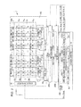
- FIG. 1 is a diagram showing a configuration of a part of a data transfer system of an electrooptic device 1 according to a first embodiment of the invention.
- FIG. 2 is a diagram schematically showing a configuration of the electrooptic device 1 .
- the electrooptic device 1 includes an electrooptic panel 100 , a first supply circuit 200 a , a second supply circuit 200 b , a flexible printed circuit board 300 a , a flexible printed circuit board 300 b , and a control circuit 500 . Ends of the flexible printed circuit boards 300 a and 300 b are connected to a side of the electrooptic panel 100 , while other ends of the flexible printed circuit boards 300 a and 300 b are connected to the control circuit 500 .
- the electrooptic device 1 has 2048 (2048 lines) pixel lines arranged side by side in a vertical direction (y direction) in the electrooptic panel 100 , while 4096 pixels are arranged in each of the pixel lines in a horizontal direction (x direction).
- the electrooptic device 1 has twice as many pixels as full high-definition devices in the horizontal direction and twice as many pixels as full high-definition devices in the vertical direction. The number of pixels included in the electrooptic device 1 may be changed.
- the electrooptic panel 100 displays gradations corresponding to any of red (R), green (G), and blue (B).
- An electrooptic device 1 R having an electrooptic panel 100 provided for R and configured to display gradations corresponding to R
- an electrooptic device 1 G having an electrooptic panel 100 provided for G and configured to display gradations corresponding to G
- an electrooptic device 1 B having an electrooptic panel 100 provided for B and configured to display gradations corresponding to B collaborate with each other to display a color image (refer to FIG. 18 ).
- the control circuit 500 generates digital data signals D ⁇ V ID for driving the pixels of the electrooptic panel 100 .
- the control circuit 500 supplies the digital data signals D ⁇ V ID to the first supply circuit 200 a and the second supply circuit 200 b .
- the control circuit 500 includes a data signal corrector 501 and an output variation corrector 502 .
- the output variation corrector 502 includes a distributing section 502 a , a storage section 502 b , and a correcting section 502 c .
- the storage section 502 b includes a storage section 502 b 1 and a storage section 502 b 2 .
- the correcting section 502 c includes a correcting section 502 c 1 and a correcting section 502 c 2 .
- Each of the flexible printed circuit boards 300 a and 300 b includes a wiring (not shown in FIG. 1 ) for transferring a signal.
- connection terminals 300 a 1 and 300 b 1 of the wirings of the flexible printed circuit boards 300 a and 300 b are connected to first and second input sections 110 a and 110 b of the electrooptic panel 100 , respectively.
- Other ends of the wirings of the flexible printed circuit boards 300 a and 300 b are connected to a control substrate (not shown) on which the control circuit 500 is mounted.
- the first supply circuit 200 a is electrically connected to the electrooptic panel 100 and the control circuit 500 via the wiring of the flexible printed circuit board 300 a
- the second supply circuit 200 b is electrically connected to the electrooptic panel 100 and the control circuit 500 via the wiring of the flexible printed circuit board 300 b.
- the first supply circuit 200 a and the second supply circuit 200 b are, for example, driving integrated circuits (driver ICs).
- the first supply circuit 200 a drives 2048 pixels that are a half of 4096 pixels included in each of the pixel lines of the electrooptic panel 100 and are arranged in the horizontal direction.
- the first supply circuit 200 a and the second supply circuit 200 b are mounted on the flexible printed circuit board 300 a and the flexible printed circuit board 300 b by a chip-on-film (COF) technique, respectively.
- COF chip-on-film
- the flexible printed circuit board 300 a is stacked on the flexible printed circuit board 300 b
- the first supply circuit 200 a is stacked on the second supply circuit 200 b .
- the flexible printed circuit board 300 a and the flexible printed circuit board 300 b are attached to the electrooptic panel 100 in such a manner that a part of the flexible printed circuit board 300 a and a part of the flexible printed circuit board 300 b overlap each other in a direction (z direction) perpendicular to a display surface of the electrooptic panel 100 .
- the first supply circuit 200 a and the second supply circuit 200 b generate data signals V ID and drive the electrooptic panel 100 based on signals received from the control circuit 500 .
- the data signals V ID have different waveforms corresponding to an image to be displayed and are analog signals.
- the first supply circuit 200 a and the second supply circuit 200 b receive the digital data signals D ⁇ V ID and various driving and control signals from the control circuit 500 .
- the digital data signals D ⁇ V ID specify, for each time range, gradations of the pixels P IX included in the electrooptic panel 100 .
- the first supply circuit 200 a and the second supply circuit 200 b generate the analog data signals V ID based on the digital data signals D ⁇ V ID and use the generated data signals V ID to drive the pixels of the electrooptic panel 100 .
- the first supply circuit 200 a includes digital-to-analog converters (D/A converters (DACs)) 200 a 1 (multiple DACs 200 a 1 are collectively shown as one DAC in FIG.
- D/A converters DACs
- the second supply circuit 200 b includes DACs 200 b 1 (multiple DACs 200 b 1 are collectively shown as one DAC in FIG. 2 ) for multiple data lines 16 for outputting data signals V ID .
- the DACs 200 a 1 and 200 b 1 convert the digital data signals D ⁇ V ID to the analog data signals V ID and output the analog data signals V ID .
- the data signals V ID generated by the first supply circuit 200 a and the data signals V ID generated by the first supply circuit 200 b are distinguished from each other, the data signals V ID generated by the first supply circuit 200 a are referred to as data signals V ID [odd], and the data signals V ID generated by the second supply circuit 200 b are referred to as data signals V ID [even].
- the digital data signal D ⁇ V ID received by the first supply circuit 200 a and the digital data signal D ⁇ V ID received by the second supply circuit 200 b are distinguished from each other, the digital data signal D ⁇ V ID received by the first supply circuit 200 a is referred to as digital data signal D ⁇ V ID [odd], and the digital data signal D ⁇ V ID received by the second supply circuit 200 b is referred to as digital data signal V ID [even].
- Each of the data signals V ID [odd] is an example of a first data signal.
- Each of the data signals V ID [even] is an example of a second data signal.
- the digital data signal D ⁇ V ID [odd] is an example of a third data signal.
- the digital data signal D ⁇ V ID [even] is an example of a fourth data signal.
- the electrooptic panel 100 includes a pixel section 10 having the plurality of pixels P IX arranged in a matrix, a distribution circuit group 21 , a scan line driving circuit 20 , a first input section 110 a , and a second input section 110 b.
- the first input section 110 a and the second input section 110 b are input terminal groups.
- the first input section 110 a receives various signals output from the first supply circuit 200 a via the flexible printed circuit board 300 a , for example.
- the second input section 110 b receives various signals output from the second supply circuit 200 b via the flexible printed circuit board 300 b , for example.
- the electrooptic panel 100 is driven based on the various signals received by the first input section 110 a and the various signals received by the second input section 110 b.
- a number M (M is a natural number) of scan lines 12 extending from the scan line driving circuit 20 in a row direction (horizontal direction or x direction) and a number N (N is a natural number) of signal lines 14 extending from the distribution circuit group 21 in a column direction (vertical direction or y direction) are formed.
- M is not limited to 2048 and may be changed and N is not limited to 4096 and may be changed.
- the number M of scan line 12 are an example of a plurality of scan lines.
- the number M of scan line 12 intersect with the number N of signal lines 14 via an insulating layer.
- the multiple pixels P IX correspond to intersections of the scan lines 12 with the signal lines 14 .
- the multiple pixels P IX are arranged in the matrix of a number M of rows arranged side by side in the vertical direction and a number N of columns arranged side by side in the horizontal direction.
- Pixels P IX display gradations corresponding to potentials of signal lines 14 upon the selection of a scan line 12 .
- An entire region of the pixel section 10 may be an effective display region. Alternatively, a part of an outer region included in the entire region of the pixel section 10 may be a non-display region.
- Scan lines 12 , signal lines 14 , and pixels P IX within the outer region of the pixel section 10 may be arranged as dummy scan lines 12 , dummy signal lines 14 , and dummy pixels P IX .
- the number J of line groups B[ 1 ] to B[J] correspond to a number J of data lines 16 [ 1 ] to 16 [J], respectively.
- a data signal V ID [odd] or a data signal V ID [even] is supplied to each of the data lines [ 1 ] to 16 [J].
- J is an even number of 2 or more
- a number K of signal lines 14 included in each of the line groups B are adjacent to each other (continuous arrangement)
- odd-numbered line groups B[odd] among the number J of line groups B[j] and even-numbered ling groups B[even] among the number J of line groups B[j] are alternately arranged.
- the line groups B[odd] include the odd-numbered line groups B[ 1 ], B[ 3 ], . . . , and B[J ⁇ 1].
- the data signals V ID [odd] including potentials specified for each time range and to be supplied to a number K of signal lines 14 belonging to each of the line groups B[odd] are output from the first supply circuit 200 a via the first input section 110 a to data lines 16 [odd] corresponding to the line groups B[odd].
- the line groups B[even] include the even-numbered line groups B[ 2 ], B[ 4 ], . . . , and B[J].
- the data signals V ID [even] including potentials specified for each time range and to be supplied to a number K of signal lines 14 belonging to each of the line groups B[even] are output from the second supply circuit 200 b via the second input section 110 b to data lines 16 [even] corresponding to the line groups B[even].
- the signal lines 14 belonging to the line groups B[odd] are an example of first signal lines, while the signal lines 14 belonging to the line groups B[even] are an example of second signal lines.
- the data signals V ID [odd] may be different from the data signals V ID [even]. If the data signals V ID [odd] are different from the data signals V ID [even], variations in the data signals V ID [odd] and the data signals V ID [even] occur, and the image quality of the electrooptic panel 100 is reduced.
- control circuit 500 individually corrects a data signal serving as a source of the digital data signal D ⁇ VID[odd] and a digital signal serving as a source of the digital data signal D ⁇ VID[even] and generates the digital data signal D ⁇ VID[odd] and the digital data signal D ⁇ VID[even].
- the correcting section 502 c 1 uses a first correction amount stored in the storage section 502 b 1 to correct the data signal (fifth data signal) serving as the source of the digital data signal D ⁇ V ID [odd] and generates the digital data signal D ⁇ V ID [odd](third data signal).
- the correcting section 502 c 2 uses a second correction amount stored in the storage section 502 b 2 to correct the data signal (sixth data signal) serving as the source of the digital data signal D ⁇ V ID [even] and generates the digital data signal D ⁇ V ID [even] (fourth data signal).
- a difference corresponding to the individual difference or the like between the first and second supply circuits 200 a and 200 b can be added between the digital data signal D ⁇ V ID [odd] and the digital data signal D ⁇ V ID [even].
- a difference, corresponding to the individual difference or the like between the first and second supply circuits 200 a and 200 b between the data signals V ID [odd] and the data signals V ID [even] can be offset or reduced by the difference between the digital data signal D ⁇ V ID [odd] and the digital data signal D ⁇ V ID [even].
- a reduction, caused by the difference between the data signals V ID [odd] and the data signals V ID [even] in the image quality can be suppressed.
- FIG. 3 is a diagram describing the operations of the electrooptic device 1 .
- the control circuit 500 outputs a vertical synchronization signal V SYNC defining vertical scan time periods V and a horizontal synchronization signal H SYNC defining horizontal scan time periods U to the scan line driving circuit 20 , the first supply circuit 200 a , and the second supply circuit 200 b .
- the control circuit 500 outputs, to the first and second supply circuits 200 a and 200 b , selection signals SEL[ 1 ] to SEL[K] and the digital data signals D ⁇ V ID that cause the polarities of the data signals V ID (potentials to be applied to liquid crystal elements 42 shown in FIG. 5 ) to be reversed in each of the vertical scan time periods V.
- the scan line driving circuit 20 sequentially outputs scan signals G[ 1 ] to G[M] to the number M of scan lines 12 in unit time periods U and sequentially selects the number M of scan lines 12 based on the horizontal synchronization signal HSYNC.
- the scan line driving circuit 20 selects a scan line 12 of an m-th row (m-th line)
- selection switches 44 (refer to FIG. 5 ) of a number N of pixels PIX of the m-th row transition to ON states.
- the first supply circuit 200 a and the second supply circuit 200 b are synchronized with the selection signals SEL[ 1 ] to SEL[K] during a time period during which the scan line 12 of the m-th row is selected, and the first supply circuit 200 a and the second supply circuit 200 b supply potentials of the data signals V ID to the corresponding signal lines 14 via the distribution circuit group 21 .
- FIG. 4 is a diagram showing the flow of a signal process.
- the data signal corrector 501 receives an image data signal I ⁇ V ID , the vertical synchronization signal V SYNC , and the horizontal synchronization signal H SYNC from a higher-level processing unit (in step S 1 ) and executes ⁇ correction on the image data signal I ⁇ V ID to generate an image data signal DI ⁇ V ID (in step S 2 ).
- the distributing section 502 a divides the image data signal DI ⁇ V ID into a first distribution image data signal DI ⁇ V ID [odd] and a second distribution image data signal DI ⁇ V ID [even] (in step S 3 ).
- the correcting section 502 c 1 corrects the first distribution image data signal DI ⁇ VID[odd] to generate the digital data signal D ⁇ VID[odd] (in step S 4 - 1 ).
- the correcting section 502 c 2 corrects the second distribution image data signal DI ⁇ VID[even] to generate the digital data signal D ⁇ VID[even] (in step S 4 - 2 ).
- control circuit 500 supplies the digital data signal D ⁇ V ID [odd], the vertical synchronization signal V SYNC , and the horizontal synchronization signal H SYNC to the first supply circuit 200 a (in step S 5 - 1 ) and supplies the digital data signal D ⁇ V ID [even], the vertical synchronization signal V SYNC , and the horizontal synchronization signal H SYNC to the second supply circuit 200 b (in step S 5 - 2 ).
- the first supply circuit 200 a sets, for each time range, the potentials of the data signals V ID [odd] to potentials corresponding to specified gradations of pixels P IX (refer to FIG. 5 ) corresponding to intersections of the scan line 12 of the m-th row with the signal lines 14 belonging to the line groups B[odd] (in step S 6 ).
- the specified gradations of the pixels P IX are defined in the digital data signal D ⁇ V ID [odd].
- the first supply circuit 200 a sequentially reverses, based on the digital data signal D ⁇ V ID [odd], the polarities of the potentials of the data signals V ID [odd] with respect to a standard potential V REF periodically (for example, in the vertical scan time periods V) in order to prevent so-called burn-in.
- the second supply circuit 200 b sets, for each time range, the potentials of the data signals V ID [even] to potentials corresponding to specified gradations of pixels P IX corresponding to intersections of the scan line 12 of the m-th row with the signal lines 14 belonging to the line groups B[even] (in step S 6 ).
- the specified gradations of the pixels P IX are defined in the digital data signal D ⁇ V ID [even].
- the second supply circuit 200 b sequentially reverses the polarities of the potentials of the data signals V ID [even] with respect to the standard potential V REF periodically (for example, in the vertical scan time periods V).
- k is a natural number of 1 ⁇ k ⁇ K
- k-th switches 40 [k] (a number J of switches 40 [k]), which are among a number K of switches 40 [ 1 ] to 40 [K] of each of distribution circuits 21 [ 1 ] to 21 [J] included in the distribution circuit group 21 , transition to ON states based on a selection signal SEL[k] output from the first supply circuit 200 a .
- the potentials of the data signals V ID are supplied to k-th signal lines 14 of the line groups B[j].
- the potentials of the data signals V ID are supplied to a number K of signal lines 14 included in each of the line groups B[j] or the number J of line groups B[ 1 ] to B[J] for each time range. Then, the potentials corresponding to the specified gradations are written in pixels P IX corresponding to intersections of the scan line 12 of the m-th row with the k-th signal lines 14 of the line groups B[j].
- the selection signal SEL[k] output from the first supply circuit 200 a is a timing signal based on the selection signal SEL[k] output from the control circuit 500 .
- control circuit 500 generates the digital data signal D ⁇ V ID [odd] and the digital data signal D ⁇ V ID [even] in order to reduce a variation in the data signals V ID [odd] and the data signals V ID [even].
- the data signal corrector 501 and the output variation corrector 502 that are included in the control circuit 500 operate as follows.
- the data signal corrector 501 executes ⁇ correction or the like on the image data signal I ⁇ V ID received from the higher-level processing unit to generate the image data signal DI ⁇ V ID .
- the image data signal DI ⁇ V ID includes polarity information indicating a positive polarity or a negative polarity.
- the output variation corrector 502 generates the digital data signal D ⁇ V ID [odd] and the digital data signal D ⁇ V ID [even] based on the image data signal DI ⁇ V ID .
- the output variation corrector 502 divides the image data signal DI ⁇ V ID into the first distribution image data signal DI ⁇ V ID [odd] and the second distribution image data signal DI ⁇ V ID [even].
- the first distribution image data signal DI ⁇ V ID [odd] is an example of a fifth data signal.
- the second distribution image data signal DI ⁇ V ID [even] is an example of a sixth data signal.
- the output variation corrector 502 individually corrects the first distribution image data signal DI ⁇ V ID [odd] and the second distribution image data signal DI ⁇ V ID [even] to generate the digital data signal D ⁇ V ID [odd] and the digital data signal D ⁇ V ID [even].
- FIG. 5 is a diagram describing the pixels P IX of the pixel section 10 .
- Each of the pixels P IX includes a liquid crystal element 42 and a selection switch 44 .
- the liquid crystal elements 42 are an example of electrooptic elements.
- Each of the liquid crystal elements 42 includes a pixel electrode 421 , a common electrode 423 arranged opposite to the pixel electrode 421 , and liquid crystal 425 located between the pixel electrode 421 and the common electrode 423 .
- the transmittance of the liquid crystal 425 changes based on a voltage applied between the pixel electrode 421 and the common electrode 423 . As described above, the polarity of the voltage to be applied is periodically reversed in order to prevent so-called burn-in.
- the voltage applied to the liquid crystal 42 when the potential of the pixel electrode 421 is higher than the potential of the common electrode 423 is referred to as “positive polarity”
- the voltage applied to the liquid crystal 42 when the potential of the pixel electrode 421 is lower than the potential of the common electrode 423 is referred to as “negative polarity”.
- the selection switch 44 is composed of an N channel type thin film transistor having a gate connected to a scan line 12 , for example.
- the selection switch 44 is located between the liquid crystal 42 (pixel electrode 421 ) and a signal line 14 and electrically controls a connection (conduction/non-conduction) between the liquid crystal 42 and the signal line 14 .
- the pixel P IX liquid crystal 42 ) displays a gradation corresponding to the potential of the signal line 14 when the selection switch 44 is controlled to be in an ON state.
- An illustration of auxiliary capacitance connected in parallel to the liquid crystal element 42 and the like is omitted. The configuration of each of the pixels P IX may be changed.
- the scan line driving circuit 20 sequentially outputs scan signals G[ 1 ] to G[M] to the number M of scan lines 12 based on the horizontal synchronization signal H SYNC in the unit time periods U and sequentially selects the number M of scan lines 12 , as shown in FIG. 3 .
- Each of the unit time periods U is set to a time length (horizontal scan time period (l H)) of one cycle of the horizontal synchronization signal H SYNC .
- the scan line driving circuit 20 sets a scan signal G[m] to be supplied to a scan line 12 of an m-th row (m-th line) to a high level (potential indicating that the scan line 12 is selected) within an m-th unit time period U among a number M of unit time periods U included in each of the vertical scan time periods V.
- a time period during which a scan line 12 is selected is also referred to as line time period and nearly corresponds to a unit time period U in the first embodiment.
- Each of the unit time periods U includes a precharge time period T PRE and a writing time period T WRT .
- a precharge time period T PRE is before a writing time period T WRT .
- a single precharge time period T PRE is before a writing time period T WRT in each of the unit time periods U.
- multiple precharge time periods T PRE may be before a writing time period T WRT .
- the data signals V ID are supplied to the signal lines 14 .
- a predetermined precharge potential V PRE (V PREa or V PREb ) is supplied to each of the signal lines 14 .
- the distribution circuit group 21 includes the number J of distribution circuits 21 [ 1 ] to 21 [J], as shown in FIG. 2 .
- the distribution circuits 21 [ 1 ] to 21 [J] correspond to the line groups B[ 1 ] to B[J], respectively.
- demultiplexers are used, for example.
- FIG. 6 is a diagram showing an example of the distribution circuits 21 [ 1 ] to 21 [J], the first supply circuit 200 a , and the second supply circuit 200 b .
- a j-th distribution circuit 21 [j] includes a number K of switches 40 [ 1 ] to 40 [K] corresponding to a number K of signal lines 14 of a j-th line group B[j].
- transistors are used, for example.
- a k-th (k is in a range of 1 to K) switch 40 [k] included in the distribution circuit 21 [j] is located between a k-th signal line 14 among the number K of signal lines 14 of the line group B[j] and a j-th data line 16 [j] among a number J of data lines 16 [ 1 ] to 16 [J] and controls an electric connection (conduction/non-conduction) between the k-th signal line 14 and the j-th data line 16 [j].
- Odd-numbered distribution circuits 21 [odd] are connected to the first supply circuit 200 a via odd-numbered data lines 16 [odd] and the first input section 110 a .
- the first supply circuit 200 a outputs the data signals V ID [odd] to the distribution circuits 21 [odd] via the first input section 110 a and the data lines 16 [odd].
- the distribution circuits 21 [odd] are connected to the first supply circuit 200 a via a first selection signal line group 60 a including a number K of first selection signal lines 60 a [ 1 ] to 60 a [K] and the first input section 110 a .
- the first supply circuit 200 a outputs a selection signal SEL[k] to the distribution circuits 21 [odd] via a k-th first selection signal line 60 a [k] included in the first selection signal line group 60 a .
- the distribution circuits 21 [odd] use the selection signals SEL[ 1 ] to SEL[K] output from the first supply circuit 200 a to distribute the data signals V ID [odd] to a number K of signal lines 14 belonging to each of the line groups B[odd].
- Even-numbered distribution circuits 21 [even] are connected to the second supply circuit 200 b via even-numbered data lines 16 [even] and the second input section 110 b .
- the second supply circuit 200 b outputs the data signals V ID [even] to the distribution circuits 21 [even] via the second input section 110 b and the data lines 16 [even].
- the distribution circuits 21 [even] are connected to the first supply circuit 200 a via the first selection signal line group 60 a .
- the first supply circuit 200 a outputs the selection signal SEL[k] to the distribution circuits 21 [even] via the k-th first selection signal line 60 a [k] included in the first selection signal line group 60 a .
- the distribution circuits 21 [even] use the selection signals SEL[ 1 ] to SEL[K] output from the first supply circuit 200 a to distribute the data signals V ID [even] to a number K of signal lines 14 belonging to each of the line groups B[even].
- the distribution circuits 21 [odd] and the distribution circuits 21 [even] are alternately arranged and adjacent to each other.
- the data signals V ID [odd] are supplied to the distribution circuits 21 [odd] via the first input section 110 a and the data lines 16 [odd].
- the data signals V ID [even] are supplied to the distribution circuits 21 [even] via the second input section 110 b and the data lines 16 [even].
- the data lines 16 [odd] and the data lines 16 [even] are alternately arranged and adjacent to each other.
- the first input section 110 a and the second input section 110 b are arranged adjacent to each other via a gap in the vertical direction (y direction) in the electrooptic panel 100 .
- a pitch of the data line 16 [j] can be smaller than pitches of the data lines 16 [odd] and pitches of the data lines 16 [even].
- the first supply circuit 200 a is an example of a first supplying section.
- the first supply circuit 200 a includes the DACs 200 a 1 for outputting the data signals V ID [odd].
- the first supply circuit 200 a supplies the selection signals SEL[ 1 ] to SEL[K] to the distribution circuits 21 [odd] and the distribution circuits 21 [even].
- the selection signals SEL[ 1 ] to SEL[K] are pulse signals that turn on the switches 40 [k] included in the distribution circuits 21 [j] during predetermined time periods.
- the first supply circuit 200 a receives the vertical synchronization signal V SYNC , the horizontal synchronization signal H SYNC , the digital data signal D ⁇ V ID [odd], and the selection signals SEL[ 1 ] to SEL[K] from the control circuit 500 .
- the first supply circuit 200 a generates the data signals V ID [odd] (first data signals) from the digital data signal D ⁇ V ID [odd] (third data signal).
- the first supply circuit 200 a outputs the data signals V ID [odd] from the DACs 200 a 1 to the data lines 16 [odd] at time corresponding to the vertical synchronization signal V SYNC and the horizontal synchronization signal H SYNC and outputs the selection signals SEL[ 1 ] to SEL[K] to the first selection signal lines 60 a [ 1 ] to 60 a [K].
- the distribution circuits 21 [odd] receive the selection signals SEL[ 1 ] to SEL[K] from the first selection signal lines 60 a [ 1 ] to 60 a [K] and use the selection signals SEL[ 1 ] to SEL[K] to distribute the data signals V ID [odd] to the signal lines 14 (first signal lines).
- the second supply circuit 200 b is an example of a second supplying section.
- the second supply circuit 200 b includes the DACs 200 b 1 for outputting the data signals V ID [even].
- the second supply circuit 200 b receives the vertical synchronization signal V SYNC , the horizontal synchronization signal H SYNC , the digital data signals D ⁇ V ID [even], and the selection signals SEL[ 1 ] to SEL[K] from the control circuit 500 .
- the second supply circuit 200 b generates the data signals V ID [even] (second data signals) from the digital data signal D ⁇ V ID [even] (fourth data signal).
- the second supply circuit 200 b outputs the data signals V ID [even] from the DACs 200 b 1 to the data lines 16 [even] at time corresponding to the vertical synchronization signal V SYNC and the horizontal synchronization signal H SYNC .
- the distribution circuits 21 [even] use the selection signals SEL[ 1 ] to SEL[K] received from the first selection signal lines 60 a [ 1 ] to 60 a [K] to distribute the data signals V ID [even] to the signal lines 14 (second signal lines).
- the second supply circuit 200 b has an output section for outputting the selection signals SEL[ 1 ] to SEL[K], but the output section is based on an open standard.
- the control circuit 500 uses various signals including the synchronization signals to control the scan line driving circuit 20 , the first supply circuit 200 a , and the second supply circuit 200 b .
- the control circuit 500 is an example of a controller that controls the first supply circuit 200 a and the second supply circuit 200 b .
- An example of functions of the control circuit 500 is described below.
- the control circuit 500 outputs the vertical synchronization signal V SYNC shown in FIG. 3 and the horizontal synchronization signal H SYNC shown in FIG. 3 to the scan line driving circuit 20 , the first supply circuit 200 a , and the second supply circuit 200 b.
- the control circuit 500 outputs, to the first supply circuit 200 a , the digital data signal D ⁇ V ID [odd] (third data signal) specifying, for each time range, gradations (gradation levels) of multiple pixels P IX (multiple first pixels) corresponding to intersections of the number M of scan lines 12 with the signal lines 14 belonging to the odd-numbered line groups B[odd].
- the control circuit 500 outputs, to the first supply circuit 200 a , the digital data signal D ⁇ V ID [odd] that causes the polarities of the data signals V ID [odd] to be reversed in each of the vertical scan time periods V, as shown in FIG. 3 .
- the data signals V ID [odd] include the potentials specified for each time range and corresponding to the gradations specified by the digital data signal D ⁇ V ID [odd] for each time range.
- the control circuit 500 outputs, to the second supply circuit 200 b , the digital data signal D ⁇ V ID [even] (fourth data signal) specifying, for each time range, gradations of multiple pixels P IX (multiple second pixels) corresponding to intersections of the number M of scan lines 12 with the signal lines 14 belonging to the even-numbered line groups B[even].
- the control circuit 500 outputs, to the second supply circuit 200 b , the digital data signal D ⁇ V ID [even] that causes the polarities of the data signals V ID [even] to be reversed in each of the vertical scan time periods V, as shown in FIG. 3 .
- the data signals V ID [even] include the potentials specified for each time range and corresponding to the gradations specified by the digital data signal D ⁇ V ID [even] in the tine ranges.
- control circuit 500 generates a number K of selection signals SEL[ 1 ] to SEL[K] corresponding to the number (number K) of signal lines 14 included in each of the line groups B[j].
- the control circuit 500 outputs the selection signals SEL[ 1 ] to SEL[K] to the first supply circuit 200 a and the second supply circuit 200 b .
- the selection signals SEL[ 1 ] to SEL[K] are timing signals that control the distribution of the data signals V ID [odd] to the signal lines 14 belonging to the line groups B[odd] and the distribution of the data signals V ID [even] to the signal lines 14 belonging to the line groups B[even].
- the control circuit 500 uses low voltage differential signaling (LVDS) to output the vertical synchronization signal V SYNC , the horizontal synchronization signal H SYNC , the digital data signal D ⁇ V ID [odd], and the selection signals SEL[ 1 ] to SEL[K] to the first supply circuit 200 a , for example.
- the control circuit 500 may use a different method from LVDS to output the vertical synchronization signal V SYNC , the horizontal synchronization signal H SYNC , the digital data signal D ⁇ V ID [odd], and the selection signals SEL[ 1 ] to SEL[K] to the first supply circuit 200 a .
- control circuit 500 uses LVDS to output the vertical synchronization signal V SYNC , the horizontal synchronization signal H SYNC , the digital data signal D ⁇ V ID [even], and the selection signals SEL[ 1 ] to SEL[K] to the second supply circuit 200 b , for example.
- the control circuit 500 may use a different method from LVDS to output the vertical synchronization signal V SYNC , the horizontal synchronization signal H SYNC , the digital data signal D ⁇ V ID [even], and the selection signals SEL[ 1 ] to SEL[K] to the second supply circuit 200 b.
- the output variation corrector 502 includes the distributing section 502 a , the storage section 502 b , and the correcting section 502 c , as shown in FIG. 2 .
- the distributing section 502 a divides the image data signal DI ⁇ V ID into the first distribution image data signal DI ⁇ V ID [odd] and the second distribution image data signal DI ⁇ V ID [even].
- the storage section 502 b includes the storage section 502 b 1 storing first correction amounts and the storage section 502 b 2 storing second correction amounts.
- the correcting section 502 c includes the correcting section 502 c 1 and the correction section 502 c 2 .
- the correcting section 502 c 1 corrects the first distribution image data signal DI ⁇ V ID [odd] using a first correction amount stored in the storage section 502 c 1 to generate the digital data signal D ⁇ V ID [odd].
- the correcting section 502 c 2 corrects the second distribution image data signal DI ⁇ V ID [even] using a second correction amount stored in the storage section 502 c 2 to generate the digital data signal D ⁇ V ID [even].
- the first correction amount is used to correct the first distribution image data signal DI ⁇ V ID [odd] and generate the digital data signal D ⁇ V ID [odd].
- the second correction amount is used to correct the second distribution image data signal DI ⁇ V ID [even] and generate the digital data signal D ⁇ V ID [even].
- the first correction amount is used to generate the digital data signal D ⁇ V ID [odd] serving as a source of the data signals V ID [odd] to be generated by the first supply circuit 200 a
- the second correction amount is used to generate the digital data signal D ⁇ V ID [even] serving as a source of the data signals V ID [even] to be generated by the second supply circuit 200 b.
- a difference corresponding to the individual difference or the like between the first and second supply circuits 200 a and 200 b can be added between the digital data signal D ⁇ V ID [odd] and the digital data signal D ⁇ V ID [even].
- the first correction amounts are stored as a lookup table (LUT) 1 - 1 and a LUT 1 - 2 in the storage section 502 b 1 .
- the LUT 1 - 1 stores first correction amounts provided for positive polarity and to be used to correct the first distribution image data signal DI ⁇ V ID [odd] having a positive polarity.
- the LUT 1 - 2 stores first correction amounts provided for negative polarity and to be used to correct the second distribution image data signal DI ⁇ V ID [odd] having a negative polarity.
- the optimal correction amount varies depending on whether the data signals V ID [odd] output from the first supply circuit 200 a have a positive polarity or a negative polarity.
- the LUT 1 - 1 storing the first correction amounts for positive polarity and the LUT 1 - 2 storing the first correction amounts for negative polarity are stored.
- the first distribution image data signal DI ⁇ V ID [odd] with a positive polarity is corrected by the correcting section 502 c 1 using a first correction amount provided for positive polarity and stored in the LUT 1 - 1 .
- the first distribution image data signal DI ⁇ V ID [odd] with a negative polarity is corrected by the correcting section 502 c 1 using a first correction amount provided for negative polarity and stored in the LUT 1 - 2 .
- the second correction amounts are stored as a LUT 2 - 1 and a LUT 2 - 2 in the storage section 502 b 2 .
- the LUT 2 - 1 stores second correction amounts provided for positive polarity and to be used to correct the second distribution image data signal DI ⁇ V ID [even] having a positive polarity.
- the LUT 2 - 2 stores second correction amounts provided for negative polarity and to be used to correct the second distribution image data signal DI ⁇ V ID [even] having a negative polarity.
- the optimal correction amount varies depending on whether the data signals V ID [even] output from the second supply circuit 200 b have a positive polarity or a negative polarity.
- the LUT 2 - 1 storing the second correction amounts for positive polarity and the LUT 2 - 2 storing the second correction amounts for negative polarity are stored.
- the second distribution image data signal DI ⁇ V ID [even] with a positive polarity is corrected by the correcting section 502 c 2 using a second correction amount provided for positive polarity and stored in the LUT 2 - 1 .
- the second distribution image data signal DI ⁇ V ID [even] with a negative polarity is corrected by the correcting section 502 c 2 using a second correction amount provided for negative polarity and stored in the LUT 2 - 2 .
- correction amounts to be used vary depending on whether the image data signal DI ⁇ V ID to be corrected has a positive polarity or a negative polarity, the correction can be executed based on the polarity.
- the first distribution image data signal DI ⁇ V ID [odd] and the second distribution image data signal DI ⁇ V ID [even] are individually corrected based on the polarity.
- a difference related to the correction based on the polarity and corresponding to the difference between the first supply circuit 200 a and the second supply circuit 200 b can be added between the digital data signal DI ⁇ V ID [odd] and the digital data signal DI ⁇ V ID [even].
- a difference, related to the correction based on the polarity, between the digital signals V ID [odd] and the digital signals V ID [even] can be offset or reduced by the difference between the digital data signal D ⁇ V ID [odd] and the digital data signal D ⁇ V ID [even]
- a reduction, caused by the difference between the data signals V ID [odd] and the data signals V ID [even] in the image quality can be suppressed.
- FIG. 9 is a diagram schematically showing the LUT 1 - 1 storing the first correction amounts for positive polarity.
- the LUT 1 - 1 is two-dimensionally configured to include gradation levels and the positions of pixels of the pixel section 10 shown in FIG. 2 in the horizontal direction (x direction) and stores the first correction amounts for positive polarity for combinations of the gradation levels and the horizontal pixel positions. Specifically, the first correction amounts are set based on the gradation levels and the horizontal pixel positions. In the first embodiment, the LUT 1 - 1 stores 25 correction amounts P 0 to P 24 for combinations of five pixel positions and five gradation levels.
- a scan signal that is transferred through a scan line 12 extending in the horizontal direction within the pixel section 10 is reduced in level due to resistance of the scan line 12 as the scan line 12 is farther from the scan line driving circuit 20 .
- the levels of scan signals in pixels arranged in the horizontal direction vary depending on the positions of the pixels arranged in the horizontal direction.
- the variation in the levels of the scan signals may cause a reduction in the image quality.
- the reduction in the image quality may be a problem with the high-definition liquid crystal display device. Since the first correction amounts are set based on the gradation levels and the horizontal pixel positions, the first correction amounts may be set to compensate for differences between the levels of the scan signals at the positions of the multiple pixels (first pixels) driven by the first supply circuit 200 a .
- the first correction amounts may be set based on the gradation levels or may not be set based on the gradation levels. If the first correction amounts are not based on the gradation levels, the LUT 1 - 1 stores the first correction amounts substantially corresponding to only the positions of pixels arranged in the horizontal direction (x direction) within the pixel section 10 .
- the first supply circuit 200 a includes the DACs 200 a 1 for the multiple data lines 16 arranged side by side in the horizontal direction within the electrooptic panel 100 , and the DACs 200 a 1 convert the digital data signal D ⁇ V ID to the analog data signals V ID and output the data signals V ID .
- the DACs 200 a 1 correspond to the multiple data lines 16 and are arranged side by side in the x direction and receive power-supply voltages from a common power supply circuit via power supply lines. Since the power supply lines have resistance, the power supply voltages supplied to the DACs 200 a 1 may vary depending on distances (lengths of the power supply lines) between the power supply circuit and the DACs 200 a 1 .
- the power supply voltages supplied to the DACs 200 a 1 may vary depending on the positions of the DACs 200 a 1 in the x direction. Output levels of the DACs 200 a 1 may vary due to the variations in the power supply voltages. Since the first correction amounts are set based on the gradation levels and the horizontal pixel positions, the first correction amounts may be set to compensate for differences between the output levels, corresponding to the positions of the DACs 200 a 1 , of the DACs 200 a 1 . In this case, the first correction amounts may be set based on the gradation levels or may not be set based on the gradation levels.
- input and output characteristics (relationships between the digital data signals D ⁇ V ID and the data signals V ID ) related to the gradation levels may vary for the DACs 200 a 1 due to individual differences between the DACs 200 a 1 .
- the first correction amounts may be set to compensate for differences between the input and output characteristics, related to the gradation levels, of the DACs 200 a 1 .
- the first correction amounts may be set based on the horizontal pixel positions or may not be set based on the horizontal pixel positions. If the first correction amounts are not set based on the horizontal pixel positions, the LUT 1 - 1 stores the first correction amounts substantially corresponding to only the gradation levels.
- the first correction amounts are set based on the gradation levels and the horizontal pixel positions, the first correction amounts may be set to compensate for the differences between the output levels, corresponding to the positions of the DACs 200 a 1 , of the DACs 200 a 1 and compensate for the differences between the input and output characteristics, related to the gradation levels, of the DACs 200 al.
- FIG. 10 is a diagram schematically showing the LUT 1 - 2 storing the first correction amounts for negative polarity.
- the LUT 1 - 2 has the same configuration as the LUT 1 - 1 , except that the LUT 1 - 2 stores 25 correction amounts M 0 to M 24 instead of the 25 correction amounts P 0 to P 24 .
- the LUT 2 - 1 storing second correction amounts for positive polarity and the LUT 2 - 2 storing second correction amounts for negative polarity are two-dimensionally configured to include the gradation levels and the horizontal pixel positions, like the LUTs 1 - 1 and 1 - 2 , and store the second correction amounts for combinations of the gradation levels and the horizontal pixel positions. Specifically, the second correction amounts are set based on the gradation levels and the horizontal pixel positions.
- the second correction amounts may be set to compensate for differences between levels of scan signals at the positions of multiple pixels (second pixels) driven by the second supply circuit 200 b , differences between output levels, corresponding to the positions of the DACs 200 b 1 , of the DACs 200 b 1 , and differences between input and output characteristics, related to the gradation levels, of the DACs 200 b 1 .
- the first supply circuit 200 a corresponding to the LUT 1 - 1 drives 2048 pixels that are a half of 4096 pixels included in each of the pixel lines and arranged in the horizontal direction within the electrooptic panel 100 .
- the second supply circuit 200 b corresponding to the LUT 2 - 1 drives remaining 2048 pixels among 4096 pixels included in each of the pixel lines and arranged in the horizontal direction within the electrooptic panel 100 .
- physically first pixels in the horizontal direction within the pixel section 10 are processed as 0th pixels
- physically 4096th pixels in the horizontal direction within the pixel section 10 are processed as 4095th pixels.
- 0th to 3rd pixels, 8th to 11th pixels, . . . , and 4088th to 4091st pixels in the horizontal direction within the electrooptic panel 100 are pixels (first pixels) driven by the first supply circuits 200 a .
- the first supply circuit 200 a executes an internal process on signals and drives 2048 pixels included in each of the pixel lines while treating the 0th to 3rd pixels in the horizontal direction within the electrooptic panel 100 as 0th to 3rd pixels, the 8th to 11th pixels in the horizontal direction within the electrooptic panel 100 as 4th to 7th pixels, . . .
- 4th to 7th pixels, 12th to 15th pixels, . . . , and 4092nd to 4095th pixels in the horizontal direction within the electrooptic panel 100 are pixels (second pixels) driven by the second supply circuit 200 b .
- the second supply circuit 200 b executes an internal process on signals and drives 2048 pixels included in each of the pixel lines while treating the 4th to 7th pixels in the horizontal direction within the electrooptic panel 100 as 0th to 3rd pixels, the 12th to 15th pixels in the horizontal direction within the electrooptic panel 100 as 4th to 7th pixels, . . . , and the 4092nd to 4095th pixels in the horizontal direction within the electrooptic panel 100 as 2044th to 2047th pixels.
- the positions of five pixels which are the 0th, 511th, 1023rd, 1535th, and 2047th pixels among 2048 pixels arranged in the horizontal direction and to be driven by the first supply circuit 200 a , are stored.
- the 0th, 511th, 1023rd, 1535th, and 2047th pixels to be driven by the first supply circuit 200 a correspond to the positions of the 4th, 1019th, 2043rd, 3067th, and 4091st pixels in the horizontal direction within the electrooptic panel 100 , respectively.
- the number of pixel positions (multiple first positions) stored in the LUT 1 - 1 are not limited to 5 and may be changed.
- the positions of five pixels which are the 0th, 511th, 1023rd, 1535th, and 2047th pixels among 2048 pixels arranged in the horizontal direction and to be driven by the second supply circuit 200 b , are stored.
- the 0th, 511th, 1023rd, 1535th, and 2047th pixels to be driven by the second supply circuit 200 b correspond to the positions of the 4th, 1023rd, 2047th, 3071st, and 4095th pixels in the horizontal direction within the electrooptic panel 100 , respectively.
- the number of pixel positions (multiple second positions) stored in the LUT 2 - 1 are not limited to 5 and may be changed.
- each of the first distribution image data signal DI ⁇ V ID [odd] and the second distribution image data signal DI ⁇ V ID [even] is a 12-bit signal
- the number of gradation levels represented by each of the first distribution image data signal DI ⁇ V ID [odd] and the second distribution image data signal DI ⁇ V ID [even] is 4096.
- the LUT 1 - 1 stores five gradation levels, a gradation 0, a gradation 1023, a gradation 2047, a gradation 3071, and a gradation 4095.
- the number of multiple gradation levels (multiple first gradation levels) stored in the LUT 1 - 1 is not limited to 5 and may be changed.
- the LUT 1 - 1 stores the 25 correction amounts P 0 to P 24 for the combinations of the five pixel positions and the five gradation levels, as shown in FIG. 9 .
- the LUT 2 - 1 stores the five gradation levels, the gradation 0, the gradation 1023, the gradation 2047, the gradation 3071, and the gradation 4095.
- the number of multiple gradation levels (multiple second gradation levels) stored in the LUT 2 - 1 is not limited to 5 and may be changed.
- the LUT 2 - 1 stores the correction amounts for the combinations of the five pixel positions and the five gradation levels.
- FIG. 11 is a diagram showing an example in which the first distribution image data signal DI ⁇ V ID [odd] is corrected in order to display the gradation 2047 on the 100th pixel driven by the first supply circuit 200 a .
- FIG. 12 is a diagram showing a position indicated by the gradation 2047 and the 100th pixel driven by the first supply circuit 200 a .
- the first distribution image data signal DI ⁇ V ID [odd] to be corrected corresponds to the position indicated by triangles.
- FIG. 13 is a flow diagram describing an operation of counting the horizontal synchronization signal H SYNC .
- the horizontal synchronization signal H SYNC is used to identify a horizontal position of a pixel to which the horizontal synchronization signal H SYNC is supplied.
- the correcting section 502 c 1 Upon receiving the vertical synchronization signal V SYNC (in step S 101 ), the correcting section 502 c 1 resets an internal counter (not shown) (in step S 102 ). After that, the correcting section 502 c 1 uses the internal counter to count the horizontal synchronization signal H SYNC (in step S 103 ). In step S 103 , the correcting section 502 c 1 repeats an operation of counting 4 pulses in the horizontal synchronization signal H SYNC and skipping counting of 4 pulses in the horizontal synchronization signal H SYNC after the counting of the 4 pulses. This count value indicates a value obtained by adding “1” to the position (number) of a pixel driven by the first supply circuit 200 a . The correcting section 502 c 1 repeats the operation shown in FIG. 13 every time the correcting section 502 c 1 receives the vertical synchronization signal V SYNC .
- FIG. 14 is a flow diagram describing a correction operation executed using the count value of the internal counter.
- the correcting section 502 c 1 uses the count value of the internal counter to determine a pixel that is among pixels driven by the first supply circuit 200 a and corresponds to the first distribution image data signal DI ⁇ V ID [odd] (in step S 201 ).
- the correcting section 502 c 1 uses the count value of the internal counter to determine that the first distribution image data signal DI ⁇ V ID [odd] corresponds to the 100th pixel driven by the first supply circuit 200 a.
- the correcting section 502 c 1 determines whether or not polarity information of the first distribution image data signal DI ⁇ V ID [odd] indicates a positive polarity (in step S 202 ). If the polarity information indicates the positive polarity (YES in step S 202 ), the correcting section 502 c 1 executes linear interpolation using correction amounts stored in the LUT 1 - 1 and calculates a correction amount to be used. If the polarity information indicates a negative polarity (NO in step S 202 ), the correcting section 502 c executes linear interpolation using correction amounts stored in the LUT 1 - 2 and calculates a correction amount to be used (in step S 204 ).
- the first distribution image data signal DI ⁇ V ID [odd] indicates the positive polarity
- the first distribution image data signal DI ⁇ V ID [odd] corresponds to the 100th pixel driven by the first supply circuit 200 a
- the correcting section 502 c 1 executes linear interpolation using the correction amounts P 10 and P 11 stored in the LUT 1 - 1 and calculates a correction amount to be used.
- the correcting section 502 c 1 executes linear interpolation using the correction amounts M 10 and M 11 stored in the LUT 1 - 2 and calculates a correction amount to be used.
- the correction amounts are not limited to values shown in FIG. 11 and may be changed.
- Whether a correction amount to be used is added to or reduced from the first distribution image data signal DI ⁇ V ID [odd] can be determined based on whether the polarity information of the first distribution image data signal DI ⁇ V ID [odd] indicates the positive polarity or the negative polarity.
- the correcting section 502 c 1 executes the addition. In this example, if the polarity information indicates the negative polarity, the correcting section 502 c 1 executes the reduction.
- the correcting section 502 c 1 executes the following calculation.
- the correcting section 502 c 1 executes the following calculation.
- FIG. 15 is a diagram showing an example in which the first distribution image data signal DI ⁇ V ID [odd] is corrected to cause the gradation 1523 to be displayed on the 0th pixel driven by the first supply circuit 200 a .
- FIG. 16 is a diagram showing a position indicated by the 0th pixel among the pixels driven by the first supply circuit 200 a and the gradation 1523 in a two-dimensional plane represented by pixel positions and gradations.
- the first distribution image data signal DI ⁇ V ID [odd] to be corrected corresponds to the position indicated by triangles.
- the correcting section 502 c 1 uses the aforementioned count value to determine that the first distribution image data signal DI ⁇ V ID [odd] corresponds to the 0th pixel driven by the first supply circuit 200 a.
- the correcting section 502 c 1 executes linear interpolation using the correction amounts P 5 and P 10 stored in the LUT 1 - 1 and calculates a correction amount to be used.
- the correcting section 502 c 1 executes linear interpolation using the correction amounts M 5 and M 10 stored in the LUT 1 - 2 and calculates a correction amount to be used.
- the correction amounts are not limited to values shown in FIG. 15 and may be changed.
- the correcting section 502 c 1 executes the following calculation.
- the correcting section 502 c 1 executes the following calculation.
- the correcting section 502 c 2 calculates, based on the gradation levels and the horizontal pixel positions, a correction amount to be used and uses the calculated correction amount to correct the second distribution image data signal DI ⁇ V ID [even] in the same manner as the correcting section 502 c 1 .
- the correcting section 502 c 2 Upon receiving the vertical synchronization signal VSYNC, the correcting section 502 c 2 resets an internal counter (not shown), like the correcting section 502 c 1 . After that, however, the correcting section 502 c 2 uses the internal counter to repeatedly execute an operation of skipping counting of 4 pulses in the horizontal synchronization signal H SYNC and counting 4 pulses in the horizontal synchronization signal H SYNC after the skipping of the counting, unlike the correcting section 502 c 1 .
- This count value indicates a value obtained by adding “1” to the position (number) of a pixel driven by the second supply circuit 200 b .
- the correcting section 502 c 2 uses this count value to determine the position of the pixel driven by the second supply circuit 200 b.
- the correcting section 502 c switches whether a correction amount (correction amount based on the first correction amount) to be used is added to or reduced from the first distribution image data signal DI ⁇ V ID [odd]. In addition, based on whether the polarities of the data signals V ID [even] are positive or negative, the correcting section 502 c switches whether a correction amount (correction amount based on the second correction amount) to be used is added to or reduced from the second distribution image data signal DI ⁇ V ID [even]. Thus, the addition or reduction of each of the correction amounts to be used can be easily set.
- the correcting section 502 c corrects the first distribution image data signal DI ⁇ V ID [odd] using a first correction amount corresponding to the positions, in the horizontal direction (extension direction of the scan lines), of the first pixels to which the data signals V ID [odd] are supplied. Then, the correcting section 502 c corrects the first distribution image data signal DI ⁇ V ID [even] using a second correction amount corresponding to the positions, in the horizontal direction, of the second pixels to which the data signals V ID [even] are supplied.
- a difference caused by the individual difference or the like between the first supply circuit 200 a and the second supply circuit 200 b and corresponding to the correction related to the pixel positions can be added between the digital data signal D ⁇ V ID [odd] and the digital data signal D ⁇ V ID [even].
- a reduction, caused by a variation in the data signals V ID [odd] and the data signals V ID [even] in the image quality can be suppressed.
- the correcting section 502 c corrects the first distribution image data signal DI ⁇ V ID [odd] using a first correction amount corresponding to the level of the first distribution image data signal DI ⁇ V ID [odd] and corrects the second distribution image data signal DI ⁇ V ID [even] using a second correction amount corresponding to the level of the second distribution image data signal DI ⁇ V ID [even].
- a difference corresponding to the correction based on the levels of the data signals can be individually reflected in the digital data signal D ⁇ V ID [odd] and the digital data signal D ⁇ V ID [even].
- the reduction, caused by the variation in the data signals V ID [odd] and the data signals V ID [even] in the image quality can be suppressed.
- the storage section 502 b 1 may not store the first correction amounts for the combinations of the gradation levels and the horizontal pixel positions and may store first correction amounts for first horizontal pixel positions, while the storage section 502 b 2 may not store the second correction amounts for the combinations of the gradation levels and the horizontal pixel positions and may store second correction amounts for second horizontal pixel positions.
- the correcting section 502 c calculates a correction amount for the first distribution image data signal DI ⁇ V ID [odd] by executing linear interpolation using first correction amounts and uses the calculated correction amount to correct the first distribution image data signal DI ⁇ V ID [odd].
- the correcting section 502 c calculates a correction amount for the second distribution image data signal DI ⁇ V ID [even] by executing linear interpolation using second correction amounts and uses the calculated correction amount to correct the second distribution image data signal DI ⁇ V ID [even].
- the storage section 502 b 1 may not store the first correction amounts for the combinations of the gradation levels and the horizontal pixel positions and may store first correction amounts for multiple first gradation levels
- the storage section 502 b 2 may not store the second correction amounts for the combinations of the gradation levels and the horizontal pixel positions and may store second correction amounts for multiple second gradation levels.
- the correcting section 502 c calculates a correction amount for the first distribution image data signal DI ⁇ V ID [odd] by executing linear interpolation using first correction amounts and uses the calculated correction amount to correct the first distribution image data signal DI ⁇ V ID [odd].
- the correcting section 502 c calculates a correction amount for the second distribution image data signal DI ⁇ V ID [even] by executing linear interpolation using second correction amounts and uses the calculated correction amount to correct the second distribution image data signal DI ⁇ V ID [even].
- the line groups B[odd] and the line groups B[even] are alternately arranged.
- a pixel section 10 included in an electrooptic device 1 A is divided into two sections in the x direction, one (pixel section 10 a ) of the two sections is driven by the first supply circuit 200 a , and the other (pixel section 10 b ) of the two sections is driven by the second supply circuit 200 b .
- the first supply circuit 200 a drives the distribution circuits 21 [ 1 ] to 21 [J/2]
- the second supply circuit 200 a drives the distribution circuits 21 [(J/2)+1] to 21 [J].
- the distribution circuits 21 [ 1 ] to 21 [J] are easily classified into a group of the distribution circuits 21 [ 1 ] to 21 [J/2] and a group of the distribution circuits 21 [(J/2)+1] to 21 [J] based on the positions of the distribution circuits 21 [ 1 ] to 21 [J], wirings between the distribution circuits 21 [ 1 ] to 21 [J], the first supply circuit 200 a , and the second supply circuit 200 b can be simplified.
- the 0th to 2047th pixels arranged in the horizontal direction within the electrooptic panel 100 are driven by the first supply circuit 200 a
- the 2048th to 4095th pixels arranged in the horizontal direction within the electrooptic panel 100 are driven by the second supply circuit 200 b .
- the correcting section 502 c 1 resets the internal counter upon receiving the vertical synchronization signal V SYNC . After the resetting, the correcting section 502 c 1 uses the internal counter to repeatedly execute an operation of counting 2048 pulses in the horizontal synchronization signal H SYNC and skipping counting of 2048 pulses in the horizontal synchronization signal H SYNC after the counting of the 2048 pulses.
- the correcting section 502 c 1 resets the internal counter upon receiving the vertical synchronization signal V SYNC . After the resetting, the correcting section 502 c 1 uses the internal counter to repeatedly execute an operation of skipping counting of 2048 pulses in the horizontal synchronization signal H SYNC and counting 2048 pulses in the horizontal synchronization signal H SYNC after the skipping of the counting of the 2048 pulses.
- the aforementioned embodiments may be variously modified. Specific modified examples are described below. Two or more examples arbitrarily selected from among the modified examples may be combined as long as there is no contradiction in the combinations.
- the electrooptic panel 100 is driven by the two first and second supply circuits 200 a and 200 b , but may be driven by three or more supply circuits including the first and second supply circuits 200 a and 200 b .
- the control circuit 500 individually correct data signals serving as sources of digital data signals to be supplied to the supply circuits and generate the digital data signals to be supplied to the supply circuits.
- the output variation corrector 502 may not correct a digital data signal related to B.
- the configurations of the LUTs 1 - 1 and 1 - 2 can be simplified.
- the second supply circuit 200 b may stop outputting the selection signals SEL[ 1 ] to SEL[K]. For example, the second supply circuit 200 b may stop outputting the selection signals SEL[ 1 ] to SEL[K] based on a stop instruction from the control circuit 500 .
- connection terminal 300 a 1 of the flexible printed circuit board 300 a and the connection terminal 300 b 1 of the flexible printed circuit board 300 b may be connected to the electrooptic panel 100 while being arranged side by side in the horizontal direction (x direction) of the electrooptic panel 100 .
- the flexible printed circuit boards 300 a and 300 b are easily attached to the electrooptic panel 100 .
- attachment regions included in the flexible printed circuit boards 300 a and 300 b and implemented in the pixel section 10 may be larger, and wirings connecting the pixel section 10 to the attachment regions may be longer, compared with the configuration in which the connection terminals 300 a 1 and 300 b 1 shown in FIG. 1 are arranged in the vertical direction (y direction).
- the control circuit 500 may supply, to the electrooptic panel 100 , a digital data signal D ⁇ RV ID for R, a digital data signal D ⁇ GV ID for G, and a digital data signal D ⁇ BV ID for B as digital data signals D ⁇ V ID sequentially (for each time range).
- Liquid crystal display devices are used as the electrooptic devices, but it is sufficient if each of the electrooptic devices includes an electrooptic substance having an optical feature that is changed by electric energy.
- the electrooptic substance corresponds to liquid crystal, organic electro luminescence (EL), or the like.
- FIG. 18 exemplifies a specific form of an electronic device having the electrooptic device according to the first embodiment or the electrooptic device according to the second embodiment.
- FIG. 18 is a schematic diagram showing a projection display device (three-plate type projector) 4000 having electrooptic devices.
- the projection display device 4000 includes the three electrooptic devices 1 ( 1 R, 1 G, and 1 B) corresponding to different display colors (red, green, and blue).
- An illumination light system 4001 supplies a red component r included in light emitted by a illumination device (light source) 4002 to the electrooptic device 1 R, supplies a green component g included in the light emitted by the illumination device 4002 to the electrooptic device 1 G, and supplies a blue component b included in the light emitted by the illumination device 4002 to the electrooptic device 1 B.
- Each of the electrooptic devices 1 functions as an optical modulator (light bulb) for modulating monochromatic light supplied from the illumination light system 4001 based on an image to be displayed.
- a projection light system 4003 synchronizes light emitted by the electrooptical devices 1 and projects the synthesized light onto a projection surface 4004 .
- the projection display device 4000 that is small in size and achieves high-definition display can be easily achieved by using the aforementioned electrooptical devices 1 .
- each of the electrooptical devices 1 R, 1 G, and 1 B may include a respective control circuit 500 .
- the electrooptical devices 1 R, 1 G, and 1 B may include the single control circuit 500 . If the electrooptical devices 1 R, 1 G, and 1 B include the single control circuit 500 , the storage section 502 b includes LUTs for first and second correction amounts for each of R, G, and B.
- Examples of the electronic device having the electrooptic device according to the first embodiment, the electrooptic device according to the second embodiment are the device exemplified in FIG. 18 , a portable personal computer, a mobile information terminal (personal digital assistant (PDA)), a digital still camera, a television, a video camera, and a car navigation system.
- examples of the electronic device are a display unit (instrument panel) for a car, an electronic organizer, electronic paper, a calculator, a word processor, a workstation, a videophone, a point-of-sale (POS) terminal, a printer, a scanner, a copier, a video player, and a device having a touch panel.
- POS point-of-sale
Abstract
Description
The correction amount for positive polarity={P11×100+P10×(512−100)}/512={10×100+0×412}/512=2.0
The output for positive polarity=(D−V ID[odd])=2047+the correction amount for positive polarity=2049
The correction amount for negative polarity={M11×100+M10×(512−100)}/512={14×100+4×412}/512=6.0
The output for negative polarity=(D−V ID[odd])=2047−the correction amount for negative polarity=2041
The correction amount for positive polarity={P10×(1523−1023)+P5×(2047−1523)}/1024={0×500+30×524}/1024=15
The output for positive polarity=(D−V ID[odd])=1523+the correction amount for positive polarity=1538
The correction amount for negative polarity={M10×(1523−1023)+M5×(2047−1523)}/1024={4×500+34×524}/1024=20
The output for negative polarity=(D−V ID[odd])=1523−the correction amount for negative polarity=1503
Claims (13)
Applications Claiming Priority (2)
| Application Number | Priority Date | Filing Date | Title |
|---|---|---|---|
| JP2016214067A JP2018072653A (en) | 2016-11-01 | 2016-11-01 | Electro-optic device, electronic apparatus, and driving method |
| JP2016-214067 | 2016-11-01 |
Publications (2)
| Publication Number | Publication Date |
|---|---|
| US20180122313A1 US20180122313A1 (en) | 2018-05-03 |
| US10380957B2 true US10380957B2 (en) | 2019-08-13 |
Family
ID=62019898
Family Applications (1)
| Application Number | Title | Priority Date | Filing Date |
|---|---|---|---|
| US15/797,755 Active 2037-11-22 US10380957B2 (en) | 2016-11-01 | 2017-10-30 | Electrooptic device, electronic device, and driving method |
Country Status (2)
| Country | Link |
|---|---|
| US (1) | US10380957B2 (en) |
| JP (1) | JP2018072653A (en) |
Cited By (1)
| Publication number | Priority date | Publication date | Assignee | Title |
|---|---|---|---|---|
| US11232766B2 (en) * | 2018-04-16 | 2022-01-25 | Beijing Boe Optoelectronics Technology Co., Ltd. | Display device, driving method thereof, and display system |
Families Citing this family (3)
| Publication number | Priority date | Publication date | Assignee | Title |
|---|---|---|---|---|
| JP2018017803A (en) * | 2016-07-26 | 2018-02-01 | セイコーエプソン株式会社 | Electro-optic device, electronic apparatus, and method for driving electro-optic device |
| CN114257608A (en) * | 2020-09-21 | 2022-03-29 | 福特全球技术公司 | Information interaction method and information interaction system |
| CN112530369B (en) * | 2020-12-25 | 2022-03-25 | 京东方科技集团股份有限公司 | Display panel, display device and driving method |
Citations (15)
| Publication number | Priority date | Publication date | Assignee | Title |
|---|---|---|---|---|
| US4760270A (en) * | 1987-06-04 | 1988-07-26 | Owens-Illinois Television Products Inc. | Method of and apparatus for comparing data signals in an electrooptical inspection system |
| JPH05216430A (en) | 1992-02-05 | 1993-08-27 | Hitachi Ltd | Data driver |
| JP2001100237A (en) | 1999-09-29 | 2001-04-13 | Advanced Display Inc | Liquid crystal display device |
| JP2001195402A (en) | 2000-01-07 | 2001-07-19 | Ricoh Co Ltd | Language processor, language processing method and storage medium stored with the method |
| US20020041263A1 (en) * | 2000-08-28 | 2002-04-11 | Seiko Epson Corporation | System and method for providing an image processing circuit that improves image quality |
| US6445720B1 (en) * | 1998-03-18 | 2002-09-03 | Oki Electric Industry Co., Ltd. | Optical output level control device for an optical wavelength multiplexer included in an optical transmission system |
| US20030020702A1 (en) * | 2001-07-27 | 2003-01-30 | Shigoru Matsuyama | Scanning line driver circuits, electrooptic apparatuses, electronic apparatuses and semiconductor devices |
| US20030030608A1 (en) * | 2001-08-09 | 2003-02-13 | Seiko Epson Corporation | Electro-optical apparatus and method of driving electro-optical material, driving circuit therefor, electronic apparatus, and display apparatus |
| US20060192699A1 (en) * | 1999-01-28 | 2006-08-31 | Semiconductor Energy Laboratory Co., Ltd. | Serial-to-parallel conversion circuit, and semiconductor display device employing the same |
| US20070057887A1 (en) * | 2005-08-18 | 2007-03-15 | Naoyuki Itakura | Display device and drive method of same |
| US20070146281A1 (en) * | 2005-11-29 | 2007-06-28 | Taizo Hosihara | Display device and driving method of display device |
| JP2009003757A (en) | 2007-06-22 | 2009-01-08 | Nippon Telegr & Teleph Corp <Ntt> | Time monitor, method and program |
| US20100014874A1 (en) * | 2005-09-20 | 2010-01-21 | National Institute Of Information And Communications Technology | Phase control optical fsk modulator |
| US20140055432A1 (en) * | 2008-06-25 | 2014-02-27 | Sony Corporation | Display device |
| US20160300534A1 (en) * | 2013-12-20 | 2016-10-13 | Sharp Kabushiki Kaisha | Display device and method for driving same |
-
2016
- 2016-11-01 JP JP2016214067A patent/JP2018072653A/en active Pending
-
2017
- 2017-10-30 US US15/797,755 patent/US10380957B2/en active Active
Patent Citations (16)
| Publication number | Priority date | Publication date | Assignee | Title |
|---|---|---|---|---|
| US4760270A (en) * | 1987-06-04 | 1988-07-26 | Owens-Illinois Television Products Inc. | Method of and apparatus for comparing data signals in an electrooptical inspection system |
| JPH05216430A (en) | 1992-02-05 | 1993-08-27 | Hitachi Ltd | Data driver |
| US6445720B1 (en) * | 1998-03-18 | 2002-09-03 | Oki Electric Industry Co., Ltd. | Optical output level control device for an optical wavelength multiplexer included in an optical transmission system |
| US20060192699A1 (en) * | 1999-01-28 | 2006-08-31 | Semiconductor Energy Laboratory Co., Ltd. | Serial-to-parallel conversion circuit, and semiconductor display device employing the same |
| JP2001100237A (en) | 1999-09-29 | 2001-04-13 | Advanced Display Inc | Liquid crystal display device |
| JP2001195402A (en) | 2000-01-07 | 2001-07-19 | Ricoh Co Ltd | Language processor, language processing method and storage medium stored with the method |
| US20020041263A1 (en) * | 2000-08-28 | 2002-04-11 | Seiko Epson Corporation | System and method for providing an image processing circuit that improves image quality |
| US20030020702A1 (en) * | 2001-07-27 | 2003-01-30 | Shigoru Matsuyama | Scanning line driver circuits, electrooptic apparatuses, electronic apparatuses and semiconductor devices |
| US20030030608A1 (en) * | 2001-08-09 | 2003-02-13 | Seiko Epson Corporation | Electro-optical apparatus and method of driving electro-optical material, driving circuit therefor, electronic apparatus, and display apparatus |
| US20070057887A1 (en) * | 2005-08-18 | 2007-03-15 | Naoyuki Itakura | Display device and drive method of same |
| US20100014874A1 (en) * | 2005-09-20 | 2010-01-21 | National Institute Of Information And Communications Technology | Phase control optical fsk modulator |
| US20070146281A1 (en) * | 2005-11-29 | 2007-06-28 | Taizo Hosihara | Display device and driving method of display device |
| US7719503B2 (en) * | 2005-11-29 | 2010-05-18 | Sony Corporation | Display device and driving method of display device |
| JP2009003757A (en) | 2007-06-22 | 2009-01-08 | Nippon Telegr & Teleph Corp <Ntt> | Time monitor, method and program |
| US20140055432A1 (en) * | 2008-06-25 | 2014-02-27 | Sony Corporation | Display device |
| US20160300534A1 (en) * | 2013-12-20 | 2016-10-13 | Sharp Kabushiki Kaisha | Display device and method for driving same |
Cited By (1)
| Publication number | Priority date | Publication date | Assignee | Title |
|---|---|---|---|---|
| US11232766B2 (en) * | 2018-04-16 | 2022-01-25 | Beijing Boe Optoelectronics Technology Co., Ltd. | Display device, driving method thereof, and display system |
Also Published As
| Publication number | Publication date |
|---|---|
| US20180122313A1 (en) | 2018-05-03 |
| JP2018072653A (en) | 2018-05-10 |
Similar Documents
| Publication | Publication Date | Title |
|---|---|---|
| CN104299552B (en) | Display device and driving method thereof | |
| EP3327716A1 (en) | Display device | |
| US7808493B2 (en) | Displaying apparatus using data line driving circuit and data line driving method | |
| US9460681B2 (en) | Display device and driving circuit thereof for improving the accuracy of gamma tuning | |
| US10255871B2 (en) | Display device including a MUX to vary voltage levels of a switching circuit used to drive a display panel | |
| US10380957B2 (en) | Electrooptic device, electronic device, and driving method | |
| US9083965B2 (en) | Stereoscopic display device | |
| CN108109572B (en) | Display device | |
| US20070268225A1 (en) | Display device, driving apparatus for display device, and driving method of display device | |
| JP2018036619A (en) | Timing controller and display device | |
| JP2011039205A (en) | Timing controller, image display device, and reset signal output method | |
| KR20160071422A (en) | Electro-optical device, driving method of electro-optical device, and electronic apparatus | |
| US20120320104A1 (en) | Image processing device, electro-optic device, electronic apparatus, and image processing method | |
| KR20110039006A (en) | Large screen liquid crystal display device | |
| US10297224B2 (en) | Electrooptical device, control method of electrooptical device, and electronic device | |
| US10290278B2 (en) | Electrooptical device, electronic device, and control method of electrooptical device | |
| US11243444B2 (en) | Display device | |
| US10199002B2 (en) | Electrooptical device, electronic apparatus, and method for driving electrooptical device | |
| US10089951B2 (en) | Display apparatus and a method of driving the same | |
| US20170316747A1 (en) | Display apparatus | |
| US10109231B2 (en) | Electrooptical device, method for controlling electrooptical device, and electronic apparatus | |
| JP2018017793A (en) | Electro-optic device and electronic apparatus | |
| KR102552303B1 (en) | Display device and driving mathod thereof | |
| US20170270875A1 (en) | Electrooptical device, control method of electrooptical device, and electronic device | |
| US20240105125A1 (en) | Display device and data driving circuit |
Legal Events
| Date | Code | Title | Description |
|---|---|---|---|
| AS | Assignment |
Owner name: SEIKO EPSON CORPORATION, JAPAN Free format text: ASSIGNMENT OF ASSIGNORS INTEREST;ASSIGNORS:MIZUSAKO, KAZUHISA;HOSAKA, HIROYUKI;SIGNING DATES FROM 20170928 TO 20170929;REEL/FRAME:043984/0379 |
|
| FEPP | Fee payment procedure |
Free format text: ENTITY STATUS SET TO UNDISCOUNTED (ORIGINAL EVENT CODE: BIG.); ENTITY STATUS OF PATENT OWNER: LARGE ENTITY |
|
| STPP | Information on status: patent application and granting procedure in general |
Free format text: NON FINAL ACTION MAILED |
|
| STPP | Information on status: patent application and granting procedure in general |
Free format text: RESPONSE TO NON-FINAL OFFICE ACTION ENTERED AND FORWARDED TO EXAMINER |
|
| STPP | Information on status: patent application and granting procedure in general |
Free format text: NOTICE OF ALLOWANCE MAILED -- APPLICATION RECEIVED IN OFFICE OF PUBLICATIONS |
|
| STCF | Information on status: patent grant |
Free format text: PATENTED CASE |
|
| MAFP | Maintenance fee payment |
Free format text: PAYMENT OF MAINTENANCE FEE, 4TH YEAR, LARGE ENTITY (ORIGINAL EVENT CODE: M1551); ENTITY STATUS OF PATENT OWNER: LARGE ENTITY Year of fee payment: 4 |