US10347776B2 - Back-surface bridge type contact electrode of crystalline silicon solar battery and preparation method therefor - Google Patents
Back-surface bridge type contact electrode of crystalline silicon solar battery and preparation method therefor Download PDFInfo
- Publication number
- US10347776B2 US10347776B2 US15/024,762 US201415024762A US10347776B2 US 10347776 B2 US10347776 B2 US 10347776B2 US 201415024762 A US201415024762 A US 201415024762A US 10347776 B2 US10347776 B2 US 10347776B2
- Authority
- US
- United States
- Prior art keywords
- electrode
- back surface
- local
- solar battery
- bridge
- Prior art date
- Legal status (The legal status is an assumption and is not a legal conclusion. Google has not performed a legal analysis and makes no representation as to the accuracy of the status listed.)
- Active
Links
Images


Classifications
-
- H01L31/022441—
-
- H—ELECTRICITY
- H10—SEMICONDUCTOR DEVICES; ELECTRIC SOLID-STATE DEVICES NOT OTHERWISE PROVIDED FOR
- H10F—INORGANIC SEMICONDUCTOR DEVICES SENSITIVE TO INFRARED RADIATION, LIGHT, ELECTROMAGNETIC RADIATION OF SHORTER WAVELENGTH OR CORPUSCULAR RADIATION
- H10F77/00—Constructional details of devices covered by this subclass
- H10F77/20—Electrodes
- H10F77/206—Electrodes for devices having potential barriers
- H10F77/211—Electrodes for devices having potential barriers for photovoltaic cells
- H10F77/219—Arrangements for electrodes of back-contact photovoltaic cells
-
- H01L31/02167—
-
- H01L31/022425—
-
- H01L31/028—
-
- H01L31/1864—
-
- H01L31/1868—
-
- H—ELECTRICITY
- H10—SEMICONDUCTOR DEVICES; ELECTRIC SOLID-STATE DEVICES NOT OTHERWISE PROVIDED FOR
- H10F—INORGANIC SEMICONDUCTOR DEVICES SENSITIVE TO INFRARED RADIATION, LIGHT, ELECTROMAGNETIC RADIATION OF SHORTER WAVELENGTH OR CORPUSCULAR RADIATION
- H10F71/00—Manufacture or treatment of devices covered by this subclass
- H10F71/128—Annealing
-
- H—ELECTRICITY
- H10—SEMICONDUCTOR DEVICES; ELECTRIC SOLID-STATE DEVICES NOT OTHERWISE PROVIDED FOR
- H10F—INORGANIC SEMICONDUCTOR DEVICES SENSITIVE TO INFRARED RADIATION, LIGHT, ELECTROMAGNETIC RADIATION OF SHORTER WAVELENGTH OR CORPUSCULAR RADIATION
- H10F71/00—Manufacture or treatment of devices covered by this subclass
- H10F71/129—Passivating
-
- H—ELECTRICITY
- H10—SEMICONDUCTOR DEVICES; ELECTRIC SOLID-STATE DEVICES NOT OTHERWISE PROVIDED FOR
- H10F—INORGANIC SEMICONDUCTOR DEVICES SENSITIVE TO INFRARED RADIATION, LIGHT, ELECTROMAGNETIC RADIATION OF SHORTER WAVELENGTH OR CORPUSCULAR RADIATION
- H10F77/00—Constructional details of devices covered by this subclass
- H10F77/10—Semiconductor bodies
- H10F77/12—Active materials
- H10F77/122—Active materials comprising only Group IV materials
-
- H—ELECTRICITY
- H10—SEMICONDUCTOR DEVICES; ELECTRIC SOLID-STATE DEVICES NOT OTHERWISE PROVIDED FOR
- H10F—INORGANIC SEMICONDUCTOR DEVICES SENSITIVE TO INFRARED RADIATION, LIGHT, ELECTROMAGNETIC RADIATION OF SHORTER WAVELENGTH OR CORPUSCULAR RADIATION
- H10F77/00—Constructional details of devices covered by this subclass
- H10F77/20—Electrodes
- H10F77/206—Electrodes for devices having potential barriers
- H10F77/211—Electrodes for devices having potential barriers for photovoltaic cells
-
- H—ELECTRICITY
- H10—SEMICONDUCTOR DEVICES; ELECTRIC SOLID-STATE DEVICES NOT OTHERWISE PROVIDED FOR
- H10F—INORGANIC SEMICONDUCTOR DEVICES SENSITIVE TO INFRARED RADIATION, LIGHT, ELECTROMAGNETIC RADIATION OF SHORTER WAVELENGTH OR CORPUSCULAR RADIATION
- H10F77/00—Constructional details of devices covered by this subclass
- H10F77/30—Coatings
- H10F77/306—Coatings for devices having potential barriers
- H10F77/311—Coatings for devices having potential barriers for photovoltaic cells
-
- Y—GENERAL TAGGING OF NEW TECHNOLOGICAL DEVELOPMENTS; GENERAL TAGGING OF CROSS-SECTIONAL TECHNOLOGIES SPANNING OVER SEVERAL SECTIONS OF THE IPC; TECHNICAL SUBJECTS COVERED BY FORMER USPC CROSS-REFERENCE ART COLLECTIONS [XRACs] AND DIGESTS
- Y02—TECHNOLOGIES OR APPLICATIONS FOR MITIGATION OR ADAPTATION AGAINST CLIMATE CHANGE
- Y02E—REDUCTION OF GREENHOUSE GAS [GHG] EMISSIONS, RELATED TO ENERGY GENERATION, TRANSMISSION OR DISTRIBUTION
- Y02E10/00—Energy generation through renewable energy sources
- Y02E10/50—Photovoltaic [PV] energy
- Y02E10/547—Monocrystalline silicon PV cells
Definitions
- the present invention relates to a back-surface bridge type contact electrode of a crystalline silicon solar battery and a preparation method therefor, and falls within the technical field of solar batteries.
- local back surface field batteries are an important research and development direction of efficient crystalline silicon solar batteries, and by means of a back surface passivation technique and a local back surface field structure, the recombination in the back surface of a solar battery can be remarkably reduced, the back reflection within long-wave bands is improved, and the absorption of free carriers in the back surface is reduced, such that the conversion efficiency of the battery is improved.
- a back surface passivation film is locally opened using a laser or chemical slurry erosion method, then an aluminium layer is formed on the back surface using a silk screen printing or evaporation method, and then aluminium atoms instead of silicon atoms enter the silicon crystal lattice in a high temperature process to form a p-type heavily-doped region, i.e. a local back surface field, below the open film region.
- the technical problem to be solved by the present invention is to overcome the deficiencies in the prior art, and provide a back-surface bridge type contact electrode of a crystalline silicon solar battery, which can inhibit the formation of voids in the local back surface field, increase the thickness of the local back surface field, reduce the resistance loss due to the fact that a minority of carriers pass through the local back surface field to the contact region to be recombined, and improve the conversion efficiency of the back passivation battery.
- a back-surface bridge type contact electrode of a crystalline silicon solar battery which comprises a local electrode connected to a local back surface field and a back surface electrode which is covered with a back surface passivation film on a contact surface with a silicon wafer substrate, at least one bridge electrode is provided between the local electrode and the back surface electrode, the contact surface of the bridge electrode and the silicon wafer substrate is also covered with the back surface passivation film, the local electrode is connected to the back surface electrode via the bridge electrode, and the back surface passivation film is also provided, besides at the connection region of the bridge electrode, between the local electrode and the back surface electrode.
- the width of the bridge electrode is 0.1-50,000 ⁇ m, and the length is 0.1-1,000 ⁇ m.
- the material of the back surface passivation film is selected from one or more of aluminium oxide, silicon oxide, silicon nitride and titanium oxide.
- the materials of the local electrode, the back surface electrode and the bridge electrode contain aluminium.
- the cross section of the local electrode is in a line or dot shape, and the dot shape includes a circle, parallelogram or regular polygon.
- the width of the local electrode is not less than 1 ⁇ m, and the spacing between the centres of the local electrodes is not less than 100 ⁇ m.
- the size of the local electrode is not less than 1 ⁇ m, and the spacing between the centres of the local electrodes is not less than 50 ⁇ m.
- the present invention further provides a method for preparing the back-surface bridge type contact electrode of a crystalline silicon solar battery, which comprises the following steps:
- the screen plate provides a gauze in the back surface electrode region and an array region composed of a plurality of local electrodes and bridge electrodes in the back-surface bridge type contact electrode of a crystalline silicon solar battery, through which a slurry can pass, and the other part is composed of a membrane which is impermeable to the slurry;
- step 1) printing a metal slurry on the back surface of the silicon wafer substrate using the screen plate in step 1) by a silk screen printing method
- the present invention further provides a method for preparing the back-surface bridge type contact electrode of a crystalline silicon solar battery, which comprises the following steps:
- the present invention has the following beneficial effects:
- the local electrode is used in the present invention to greatly reduce the probability of voids appearing in the local back surface field, and improve the open circuit voltage and the fill factor of the battery; and the formation of the local electrode in the open film region in the present invention restricts the transversal transmission of silicon in the electrode in the high temperature process, and if each electrode contains aluminium, it can enable the concentration of silicon in the aluminium-silicon liquid alloy to rapidly reach the saturation value, and silicon is rapidly precipitated from the aluminium silicon liquid in a temperature decreasing process and solidified at the aluminium-silicon interface to form a local back surface field, which greatly inhibits the generation of voids;
- the bridge electrode is used to conduct the electric current collected in the local electrode to the back surface electrode, and using the bridge electrode and the back surface electrode reduces the resistance of the back surface electrode, thereby reducing the resistance loss of the battery;
- the process of the present invention is simple, can achieve the structure of the present invention by only printing once with regard to conventional silk screen printing, and is suitable for use in large-scale production.
- FIG. 1 is a structure schematic view of a first structure of a back-surface bridge type contact electrode of a crystalline silicon solar battery of the present invention
- FIG. 2 is a structure section view of the back-surface bridge type contact electrode of a crystalline silicon solar battery of the present invention
- FIG. 3 is a structure schematic view of a third structure of the back-surface bridge type contact electrode of a crystalline silicon solar battery of the present invention.
- FIG. 4 is a structure schematic view of a fourth structure of the back-surface bridge type contact electrode of a crystalline silicon solar battery of the present invention.
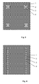
- FIG. 5 is a structure schematic view of an array form of the third structure of the back-surface bridge type contact electrode of a crystalline silicon solar battery of the present invention.
- FIG. 6 is a structure schematic view of an array form of the fourth structure of the back-surface bridge type contact electrode of a crystalline silicon solar battery of the present invention.
- a back-surface bridge type contact electrode of a crystalline silicon solar battery which comprises a local electrode 3 connected to a local back surface field 5 and a back surface electrode 1 which is covered with a back surface passivation film 2 on a contact surface with a silicon wafer substrate 6 , four bridge electrodes 4 are provided between the local electrode 3 and the back surface electrode 1 , the contact surface of the bridge electrodes 4 and the silicon wafer substrate 6 is also covered with the back surface passivation film 2 , the local electrode 3 is connected to the back surface electrode 1 via the bridge electrodes 4 , and the back surface passivation film 2 is also provided, besides at the connection region of the bridge electrodes 4 , between the local electrode 3 and the back surface electrode 1 .
- the material of the back surface passivation film 2 may be selected from one or more of aluminium oxide, silicon oxide, silicon nitride and titanium oxide.
- the materials of the local electrode 3 , the back surface electrode 1 and the bridge electrodes 4 contain aluminium.
- This embodiment provides a circular hole-shaped array of back-surface bridge type contact electrodes of a crystalline silicon solar battery, which is prepared through silk screen printing, and after the deposition of an Al 2 O 3 /SiN x : H passivation film on the back surface is complete, the film is opened using a chemical slurry.
- a screen plate design the use of silk screen printing and a well designed back surface screen plate, an aluminium slurry is printed on the back surface to make it form a pattern formed by an array of a plurality of circular holes, wherein the spacing between the circular hole contacts is 500 ⁇ m, the pattern of a single circular hole point contact is as shown in FIG.
- the diameter of the circular hole is 100 ⁇ m
- the distance between the edge of the circular hole and the back surface electrode 1 which is covered on the Al 2 O 3 /SiN x : H passivation film 2 is 20 ⁇ m
- the circular hole is connected to the back surface electrode 1 via four channels in the process of printing, the width of the channels are 50 ⁇ m, and the length thereof is equal to the distance between the edge of the circular hole and the back surface electrode 1 , i.e. also 20 ⁇ m.
- the circular hole and the silicon wafer substrate 6 therebelow form a local back surface field 5
- the circular hole also forms a local electrode 3
- the bridge electrodes 4 are formed inside the channels
- the local electrode 3 is interconnected with the back surface electrode 1 via the four bridge electrodes 4 . Since besides the place in contact with the bridge electrodes 4 , the local electrode 3 and the back surface electrode 1 are isolated by the Al 2 O 3 /SiN x : H passivation film, the diffusion of silicon in the aluminium-silicon alloy liquid is restricted in the high temperature process, which thus greatly reduces the generation of voids.
- the void rate is 100%; however, if using the method provided by the present invention, the void rate is reduced to 20% from 100%, and is effectively reduced.
- a back-surface bridge type contact electrode of a crystalline silicon solar battery which comprises a local electrode 3 connected to a local back surface field 5 and a back surface electrode 1 which is covered with a back surface passivation film 2 on a contact surface with a silicon wafer substrate 6 , two bridge electrodes 4 are provided between the local electrode 3 and the back surface electrode 1 , the contact surface of the bridge electrodes 4 and the silicon wafer substrate 6 is also covered with the back surface passivation film 2 , the local electrode 3 is connected to the back surface electrode 1 via the bridge electrodes 4 , and the back surface passivation film 2 is also provided, besides at the connection region of the bridge electrodes 4 , between the local electrode 3 and the back surface electrode 1 .
- the material of the back surface passivation film 2 may be selected from one or more of aluminium oxide, silicon oxide, silicon nitride and titanium oxide.
- the materials of the local electrode 3 , the back surface electrode 1 and the bridge electrodes 4 contain aluminium.
- This embodiment provides a square hole-shaped array of back-surface bridge type contact electrodes of a crystalline silicon solar battery, which is prepared through silk screen printing, and after the deposition of an Al 2 O 3 /SiN x : H passivation film 2 on the back surface and the local opening of the film with a laser are complete, through a screen plate design, an aluminium slurry is printed on the back surface using silk screen printing to make it form a pattern formed by the array of square holes.
- the spacing between the centres of the square holes is 400 ⁇ m, the pattern of a single square hole point contact is as shown in FIG.
- the side length of the square hole is 80 ⁇ m
- the distance between the edge of the square hole and the back surface electrode 1 is 30 ⁇ m
- two bridge electrodes 4 connecting the square hole and the back surface electrode 1 are further formed in the same printing, the width of the bridge electrodes 4 being 40 ⁇ m, the length thereof being 30 ⁇ m.
- the local electrode 3 and the back surface electrode 1 are isolated by the Al 2 O 3 /SiN x : H passivation film 2 , by using the method provided by the present invention, the void rate is reduced to 22% from 90%, and a part of the square hole point contact array on the back surface is as shown in FIG. 5 .
- a back-surface bridge type contact electrode of a crystalline silicon solar battery which comprises a local electrode 3 connected to a local back surface field 5 and a back surface electrode 1 which is covered with a back surface passivation film 2 on a contact surface with a silicon wafer substrate 6 , a plurality of bridge electrodes 4 are provided between the local electrode 3 and the back surface electrode 1 , the contact surface of the bridge electrodes 4 and the silicon wafer substrate 6 is also covered with the back surface passivation film 2 , the local electrode 3 is connected to the back surface electrode 1 via the bridge electrodes 4 , and the back surface passivation film 2 is also provided, besides at the connection region of the bridge electrodes 4 , between the local electrode 3 and the back surface electrode 1 .
- the material of the back surface passivation film 2 may be selected from one or more of aluminium oxide, silicon oxide, silicon nitride and titanium oxide.
- the materials of the local electrode 3 , the back surface electrode 1 and the bridge electrodes 4 contain aluminium.
- This embodiment provides a back-surface bridge type contact electrode of a crystalline silicon solar battery, which is prepared through silk screen printing, wherein a screen plate required for the silk screen printing is designed first, and after the deposition of an Al 2 O 3 /SiN x : H passivation film on the back surface and the local opening of the film with a laser are complete, silk screen printing and a well designed back surface screen plate are used and an aluminium slurry is printed on the back surface, so as to make it form a pattern formed by a line-shaped array.
- the spacing between the lines is 1200 ⁇ m, and a part of the line-shaped array on the back surface is as shown in FIG. 6 .
- the line width is 60 ⁇ m
- the line length is 153 mm
- the distance between the line edge and the back surface electrode 1 which is covered on the back surface Al 2 O 3 /SiN x : H passivation film is 30 ⁇ m
- the bridge electrodes 4 having a width of 40 ⁇ m, a length of 30 ⁇ m and a spacing of 1 mm are further formed in the same printing.
- the local electrode 3 in the line together with the silicon wafer substrate 6 therebelow forms a local back surface field 5 , and is connected to the back surface electrode 1 via the array of bridge electrodes 4 .
- the void rate is reduced to 17% from 100%.
- a back-surface bridge type contact electrode of a crystalline silicon solar battery which comprises a local electrode 3 connected to a local back surface field 5 and a back surface electrode 1 which is covered with a back surface passivation film 2 on a contact surface with a silicon wafer substrate 6 , at least one bridge electrode 4 is provided between the local electrode 3 and the back surface electrode 1 , the contact surface of the bridge electrode 4 and the silicon wafer substrate 6 is also covered with the back surface passivation film 2 , the local electrode 3 is connected to the back surface electrode 1 via the bridge electrode 4 , and the back surface passivation film 2 is also provided, besides at the connection region of the bridge electrode 4 , between the local electrode 3 and the back surface electrode 1 .
- the width of the bridge electrode 4 may be 0.1-50,000 ⁇ m, and the length may be 0.1-1,000 ⁇ m.
- the material of the back surface passivation film 2 may be selected from one or more of aluminium oxide, silicon oxide, silicon nitride and titanium oxide.
- the materials of the local electrode 3 , the back surface electrode 1 and the bridge electrode 4 contain aluminium.
- the cross section of the local electrode 3 can be in a line or dot shape, and the dot shape includes a circle, parallelogram or regular polygon.
- the width of the local electrode 3 is not less than 1 ⁇ m, and the spacing between the centres of the local electrodes 3 is not less than 100 ⁇ m.
- the size of the local electrode 3 is not less than 1 ⁇ m, and the spacing between the centres of the local electrodes 3 is not less than 50 ⁇ m.
- a method for preparing the back-surface bridge type contact electrode of a crystalline silicon solar battery comprises the following steps:
Landscapes
- Photovoltaic Devices (AREA)
- Life Sciences & Earth Sciences (AREA)
- Engineering & Computer Science (AREA)
- Sustainable Development (AREA)
- Sustainable Energy (AREA)
Abstract
Description
Claims (11)
Applications Claiming Priority (4)
| Application Number | Priority Date | Filing Date | Title |
|---|---|---|---|
| CN201310440907.5 | 2013-09-25 | ||
| CN201310440907 | 2013-09-25 | ||
| CN201310440907.5A CN103474486B (en) | 2013-09-25 | 2013-09-25 | Back bridge type contact electrode of crystal-silicon solar cell and preparation method thereof |
| PCT/CN2014/083399 WO2015043311A1 (en) | 2013-09-25 | 2014-07-31 | Back bridge type contact electrode of crystalline silicon solar cell and preparation method therefor |
Publications (2)
| Publication Number | Publication Date |
|---|---|
| US20160233356A1 US20160233356A1 (en) | 2016-08-11 |
| US10347776B2 true US10347776B2 (en) | 2019-07-09 |
Family
ID=49799271
Family Applications (1)
| Application Number | Title | Priority Date | Filing Date |
|---|---|---|---|
| US15/024,762 Active US10347776B2 (en) | 2013-09-25 | 2014-07-31 | Back-surface bridge type contact electrode of crystalline silicon solar battery and preparation method therefor |
Country Status (4)
| Country | Link |
|---|---|
| US (1) | US10347776B2 (en) |
| JP (1) | JP6407263B2 (en) |
| CN (1) | CN103474486B (en) |
| WO (1) | WO2015043311A1 (en) |
Families Citing this family (8)
| Publication number | Priority date | Publication date | Assignee | Title |
|---|---|---|---|---|
| CN103474486B (en) | 2013-09-25 | 2015-12-23 | 常州天合光能有限公司 | Back bridge type contact electrode of crystal-silicon solar cell and preparation method thereof |
| CN105470319B (en) * | 2015-12-22 | 2019-01-22 | 西安交通大学苏州研究院 | Preparation method of point contact back electrode structure for crystalline silicon solar cell |
| CN105576051B (en) * | 2016-02-22 | 2017-11-03 | 苏州阿特斯阳光电力科技有限公司 | The deposition process of crystal silicon cell backplate and obtained crystal silicon cell |
| CN106876486B (en) * | 2017-03-24 | 2018-11-09 | 浙江隆基乐叶光伏科技有限公司 | String formation connection structure, component and the method for P-type crystal silicon back contacts double-side cell |
| CN110462845B (en) * | 2017-03-27 | 2023-01-13 | 东洋铝株式会社 | Paste composition for solar cell |
| JP2019009401A (en) * | 2017-06-28 | 2019-01-17 | 東洋アルミニウム株式会社 | Solar cell electrode |
| CN111742418B (en) * | 2018-02-23 | 2023-08-29 | 株式会社钟化 | Solar cell and electronic device provided with same |
| CN121692858A (en) * | 2026-02-12 | 2026-03-17 | 浙江晶科能源有限公司 | A solar cell and photovoltaic module |
Citations (9)
| Publication number | Priority date | Publication date | Assignee | Title |
|---|---|---|---|---|
| US20080061293A1 (en) * | 2005-01-20 | 2008-03-13 | Commissariat A'energie Atomique | Semiconductor Device with Heterojunctions and an Inter-Finger Structure |
| US20100032014A1 (en) * | 2007-03-28 | 2010-02-11 | Commissariat A L'energie Atomique | Photovoltaic device with a discontinuous interdigitated heterojunction structure |
| US20100126573A1 (en) * | 2008-11-26 | 2010-05-27 | Microlink Devices, Inc. | Solar cell with a backside via to contact the emitter layer |
| US20110011440A1 (en) * | 2008-03-31 | 2011-01-20 | Masaomi Hioki | Solar cell, solar cell string and solar cell module |
| US20120012176A1 (en) * | 2010-07-19 | 2012-01-19 | Young-Jin Kim | Solar cell and method of manufacturing the same |
| CN102437246A (en) | 2011-12-20 | 2012-05-02 | 日地太阳能电力股份有限公司 | Preparation method of crystalline silicon solar cell |
| TW201248873A (en) | 2011-05-16 | 2012-12-01 | Motech Ind Inc | Solar cell with back surface field structure and manufacturing method thereof |
| KR20130065446A (en) | 2011-12-09 | 2013-06-19 | 삼성전자주식회사 | Solar cell |
| CN103474486A (en) | 2013-09-25 | 2013-12-25 | 常州天合光能有限公司 | Back bridge type contact electrode of crystalline silicon solar cell and preparation method thereof |
Family Cites Families (6)
| Publication number | Priority date | Publication date | Assignee | Title |
|---|---|---|---|---|
| US7461575B2 (en) * | 2006-04-26 | 2008-12-09 | Jerry Walter Tribby | Spark plug wrench for confined spaces |
| US20120037224A1 (en) * | 2009-04-29 | 2012-02-16 | Mitsubishi Electric Corporation | Solar battery cell and method of manufacturing the same |
| CN201699033U (en) * | 2010-03-30 | 2011-01-05 | 杨乐 | Two-sided illuminated crystalline silicon solar battery |
| WO2012002780A2 (en) * | 2010-07-01 | 2012-01-05 | Samsung Electronics Co., Ltd. | Composition for light-emitting particle-polymer composite, light-emitting particle-polymer composite, and device including the light-emitting particle-polymer composite |
| DE102010036893B4 (en) * | 2010-08-06 | 2017-01-19 | Hanwha Q.CELLS GmbH | Manufacturing method of a semiconductor device |
| CA2714130A1 (en) * | 2010-08-31 | 2012-02-29 | Ervis Hyseni | Electronic device case gripper |
-
2013
- 2013-09-25 CN CN201310440907.5A patent/CN103474486B/en active Active
-
2014
- 2014-07-31 US US15/024,762 patent/US10347776B2/en active Active
- 2014-07-31 WO PCT/CN2014/083399 patent/WO2015043311A1/en not_active Ceased
- 2014-07-31 JP JP2016517450A patent/JP6407263B2/en active Active
Patent Citations (9)
| Publication number | Priority date | Publication date | Assignee | Title |
|---|---|---|---|---|
| US20080061293A1 (en) * | 2005-01-20 | 2008-03-13 | Commissariat A'energie Atomique | Semiconductor Device with Heterojunctions and an Inter-Finger Structure |
| US20100032014A1 (en) * | 2007-03-28 | 2010-02-11 | Commissariat A L'energie Atomique | Photovoltaic device with a discontinuous interdigitated heterojunction structure |
| US20110011440A1 (en) * | 2008-03-31 | 2011-01-20 | Masaomi Hioki | Solar cell, solar cell string and solar cell module |
| US20100126573A1 (en) * | 2008-11-26 | 2010-05-27 | Microlink Devices, Inc. | Solar cell with a backside via to contact the emitter layer |
| US20120012176A1 (en) * | 2010-07-19 | 2012-01-19 | Young-Jin Kim | Solar cell and method of manufacturing the same |
| TW201248873A (en) | 2011-05-16 | 2012-12-01 | Motech Ind Inc | Solar cell with back surface field structure and manufacturing method thereof |
| KR20130065446A (en) | 2011-12-09 | 2013-06-19 | 삼성전자주식회사 | Solar cell |
| CN102437246A (en) | 2011-12-20 | 2012-05-02 | 日地太阳能电力股份有限公司 | Preparation method of crystalline silicon solar cell |
| CN103474486A (en) | 2013-09-25 | 2013-12-25 | 常州天合光能有限公司 | Back bridge type contact electrode of crystalline silicon solar cell and preparation method thereof |
Non-Patent Citations (1)
| Title |
|---|
| English machine translation of TW 201248873 A1 (Year: 2017). * |
Also Published As
| Publication number | Publication date |
|---|---|
| WO2015043311A1 (en) | 2015-04-02 |
| US20160233356A1 (en) | 2016-08-11 |
| JP2016533635A (en) | 2016-10-27 |
| CN103474486B (en) | 2015-12-23 |
| CN103474486A (en) | 2013-12-25 |
| JP6407263B2 (en) | 2018-10-17 |
Similar Documents
| Publication | Publication Date | Title |
|---|---|---|
| US10347776B2 (en) | Back-surface bridge type contact electrode of crystalline silicon solar battery and preparation method therefor | |
| AU2013326971B2 (en) | Photovoltaic devices with electroplated metal grids | |
| CN103489934B (en) | Local aluminum back surface field solar cell of a kind of transparent two sides and preparation method thereof | |
| CN102763225B (en) | High-efficiency photovoltaic back-junction back-contact solar cell structure and fabrication method using semiconductor wafer | |
| CN102403371B (en) | Solar cells with electroplated metal grids | |
| JP6300712B2 (en) | Solar cell and method for manufacturing solar cell | |
| CN102496661A (en) | Preparation method of back electric field contact crystalline silica solar cell | |
| CN102184985B (en) | Back face passivating structure and method for floating junction of solar cell | |
| CN105576051B (en) | The deposition process of crystal silicon cell backplate and obtained crystal silicon cell | |
| CN208570638U (en) | Solar battery grid line structure, solar battery sheet and solar energy stacked wafer moudle | |
| TW201244144A (en) | Improved a-Si:H absorber layer for a-Si single-and multijunction thin film silicon solar cell | |
| CN203521433U (en) | Back bridge contact electrodes of crystalline silicon solar cells | |
| CN103077984A (en) | Double-PIN junction double-sided solar cell with N-type silicon substrate | |
| CN103022166A (en) | Solar cell taking copper-clad aluminum wire as back electrode and producing process of solar cell | |
| CN106298984A (en) | Solar cell | |
| CN214313220U (en) | A double-sided Local BSF solar cell | |
| JP6743286B2 (en) | Photoelectric conversion element and method for manufacturing photoelectric conversion element | |
| TWI705572B (en) | Solar cell having silicon oxynitride passivation layer and method for manufacturing the same | |
| CN204391124U (en) | A kind of passivating back solar cell | |
| CN202996853U (en) | Double-PIN junction two-face solar cell with N-type silicon substrate | |
| CN202996909U (en) | Double-face heterojunction solar cell sheet with N-type silicon substrate and organic crystal | |
| CN104253166A (en) | Back-contact solar cell and preparation method thereof | |
| TWM500984U (en) | Silicon-based photovoltaic device | |
| CN103066208A (en) | N type silicon substrate and organic crystal double-face heterojunction solar battery type |
Legal Events
| Date | Code | Title | Description |
|---|---|---|---|
| AS | Assignment |
Owner name: CHANGZHOU TRINA SOLAR ENERGY CO., LTD., CHINA Free format text: ASSIGNMENT OF ASSIGNORS INTEREST;ASSIGNORS:CHEN, YIFENG;VERLINDEN, PIERRE J.;FENG, ZHIQIANG;AND OTHERS;REEL/FRAME:038118/0001 Effective date: 20160320 |
|
| STPP | Information on status: patent application and granting procedure in general |
Free format text: NOTICE OF ALLOWANCE MAILED -- APPLICATION RECEIVED IN OFFICE OF PUBLICATIONS |
|
| AS | Assignment |
Owner name: TRINA SOLAR LTD., CHINA Free format text: CHANGE OF NAME;ASSIGNOR:CHANGZHOU TRINA SOLAR ENERGY CO., LTD.;REEL/FRAME:049288/0606 Effective date: 20171122 Owner name: TRINA SOLAR CO., LTD., CHINA Free format text: CHANGE OF NAME;ASSIGNOR:TRINA SOLAR LTD.;REEL/FRAME:049288/0624 Effective date: 20171228 |
|
| STPP | Information on status: patent application and granting procedure in general |
Free format text: PUBLICATIONS -- ISSUE FEE PAYMENT VERIFIED |
|
| STCF | Information on status: patent grant |
Free format text: PATENTED CASE |
|
| MAFP | Maintenance fee payment |
Free format text: PAYMENT OF MAINTENANCE FEE, 4TH YEAR, LARGE ENTITY (ORIGINAL EVENT CODE: M1551); ENTITY STATUS OF PATENT OWNER: LARGE ENTITY Year of fee payment: 4 |