CROSS REFERENCE TO RELATED APPLICATIONS
This application claims the benefit of priority to Japanese Patent Application No. 2015-060087 filed on Mar. 23, 2015 and is a Continuation Application of PCT Application No. PCT/JP2016/051337 filed on Jan. 18, 2016. The entire contents of each application are hereby incorporated herein by reference.
BACKGROUND OF THE INVENTION
1. Field of the Invention
The present invention relates to a band pass filter. More particularly, the present invention relates to a band pass filter in which magnetic coupling between inductors of adjacent LC parallel resonators is easily adjusted.
Furthermore, the present invention relates to a laminate band pass filter in which the above-described band pass filter includes a multilayer body in which insulating layers are laminated one on top of another. More particularly, the present invention relates to a laminate band pass filter in which magnetic coupling between the inductors of the adjacent LC parallel resonators is easily adjusted.
2. Description of the Related Art
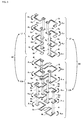
International Publication No. WO2009/041294A1 discloses a band pass filter which includes a plurality of LC parallel resonators and in which inductors of the adjacent LC parallel resonators are magnetically coupled.
FIGS. 11 and 12 illustrate a band pass filter 500 disclosed in International Publication No. WO2009/041294A1. FIG. 11 is an exploded perspective view of the band pass filter 500. FIG. 12 is an equivalent circuit diagram of the band pass filter 500.
As illustrated in FIG. 11, the band pass filter 500 includes a multilayer body 107 in which six insulating layers (dielectric layers) 101 to 106 are sequentially laminated from the bottom. The following electrodes are provided on the multilayer body 107.
A ground electrode 109 is provided on the insulating layer 101. The ground electrode 109 is connected to ground terminals 151 and 152 that extend to side surfaces of the multilayer body 107.
Capacitor electrodes 111, 112, and 113 are provided on the insulating layer 102.
Input/output terminals (input/output electrodes) 121 and 122 and a capacitor electrode (capacitor between input and output) 160 are provided on the insulating layer 103.
An S-shaped line electrode 117 is provided on the insulating layer 104.
C- shaped line electrodes 116 and 118 are provided on the insulating layer 105. The line electrode 116 and the line electrode 118 are line symmetrically (also, point symmetrically) arranged.
No electrode is provided on the insulating layer 106.
Via electrodes 131 and 135 are that penetrates through the insulating layers 103 to 105. The via electrode 131 has one end connected to the capacitor electrode 111 and the other end connected to one end 116A of the line electrode 116 and is connected to the first input/output terminal 121 through an extended electrode 121A between the one and the other ends thereof. The via electrode 135 has one end connected to the capacitor electrode 113 and the other end connected to one end 118A of the line electrode 118 and is connected to the second input/output terminal 122 through an extended electrode 122A between the one and the other ends thereof.
Via electrodes 132 and 136 are that penetrates through the insulating layers 102 to 105. The via electrode 132 has one end connected to the ground electrode 109 and the other end connected to the other end 116B of the line electrode 116. The via electrode 136 has one end connected to the ground electrode 109 and the other end connected to the other end 118B of the line electrode 118.
A via electrode 133 is that penetrates through the insulating layers 102 to 104. The via electrode 133 has one end connected to the ground electrode 109 and the other end connected to one end 117A of the line electrode 117.
A via electrode 134 is that penetrates through the insulating layers 103 and 104. The via electrode 134 has one end connected to the capacitor electrode 112 and the other end connected to the other end 117B of the line electrode 117.
The band pass filter 500 disclosed in International Publication No. WO2009/041294A1 has the equivalent circuit illustrated in FIG. 12.
The band pass filter 500 includes an LC parallel resonator at a first stage (input stage) that includes an inductor L1 and a capacitor C1, an LC parallel resonator at a second stage (intermediate stage) that includes an inductor L2 and a capacitor C2, and an LC parallel resonator at a third stage (output stage) that includes an inductor L3 and a capacitor C3.
One end of the LC parallel resonator at the first stage, a capacitor C12, one end of the LC parallel resonator at the second stage, a capacitor C23, one end of the LC parallel resonator at the third stage are sequentially connected between a first input/output terminal (IN) and a second input/output terminal (OUT).
The other end of the LC parallel resonator at the first stage, the other end of the LC parallel resonator at the second stage, and the other end of the LC parallel resonator at the third stage are connected to a ground terminal.
A capacitor C13 is connected in parallel with the capacitor C12 and the capacitor C23 that are connected in series.
Three LC parallel resonators are in capacitive coupling with one another by using the capacitors C12, C13, and C23. Furthermore, the inductor L1 of the first LC parallel resonator and the inductor L2 of the second LC parallel resonator are in magnetic coupling M1 with each other, and the inductor L2 of the second LC parallel resonator and the inductor L3 of the third LC parallel resonator are in magnetic coupling M2 with each other.
Next, referring to FIGS. 11 and 12, the relationship between the structure of the band pass filter 500 and the equivalent circuit of the band pass filter 500 is described.
The inductor L1 of the LC parallel resonator at the first stage is defined by a path that connects the extended electrode 121A, the via electrode 131, the one end 116A of the line electrode 116, a main body portion of the line electrode 116, the other end 116B of the line electrode 116, the via electrode 132, and the ground electrode 109.
The capacitor C1 of the LC parallel resonator at the first stage is defined by capacitance generated between the capacitor electrode 111 and the ground electrode 109. The first input/output terminal 121 and the capacitor C1 are connected to each other through the extended electrode 121A and the via electrode 131.
The inductor L2 of the LC parallel resonator at the second stage is defined by a path that connects the capacitor electrode 112, the via electrode 134, the other end 117B of the line electrode 117, a main body portion of the line electrode 117, the one end 117A of the line electrode 117, the via electrode 133, and the ground electrode 109.
The capacitor C2 of the LC parallel resonator at the second stage is defined by capacitance generated between the capacitor electrode 112 and the ground electrode 109.
The inductor L3 of the LC parallel resonator at the third stage is defined by a path that connects the extended electrode 122A, the via electrode 135, the one end 118A of the line electrode 118, a main body portion of the line electrode 118, the other end 118B of the line electrode 118, the via electrode 136, and the ground electrode 109.
The capacitor C3 of the LC parallel resonator at the third stage is defined by capacitance generated between the capacitor electrode 113 and the ground electrode 109. The second input/output terminal 122 and the capacitor C3 are connected to each other through the extended electrode 122A and the via electrode 135.
The capacitor C12 is defined by capacitance generated between the capacitor electrodes 111 and 112.
The capacitor C23 is defined by capacitance generated between the capacitor electrodes 112 and 113.
The capacitor C13 is defined by resultant capacitance of capacitance generated between capacitor electrode 111 and the capacitor electrode 113, capacitance generated between the capacitor electrode 160 between the input and output and the extended electrodes 121A and 122A, and capacitance generated between both end portions of the capacitor electrode 160 between the input and output and the capacitor electrodes 111 and 113.
FIG. 13 illustrates the positional relationship between the line electrode 116 and the line electrode 117 and the positional relationship between the line electrode 117 and the line electrodes 118 in the band pass filter 500. Also, the direction of a current of the inductor L1 flowing through the line electrode 116 is indicated by an arrow AL1, the direction of a current of the inductor L2 flowing through the line electrode 117 is indicated by an arrow AL2, and the direction of a current of the inductor L3 flowing through the line electrode 118 is indicated by an arrow AL3. Furthermore, the magnetic coupling between the inductor L1 and the inductor L2 is indicated by M1, and the magnetic coupling between the inductor L1 and the inductor L2 is indicated by M2.
The line electrode 116 and the line electrode 117 are superposed on each other and the line electrode 117 and the line electrode 118 are superposed on each other in the band pass filter 500.
However, since the line electrode 117 has an S-shape, the line electrode 116 and the line electrode 117 are not superposed on each other in part of the band pass filter 500. Likewise, the line electrode 117 and the line electrode 118 are not superposed on each other in part of the band pass filter 500.
Since there exists the part where the line electrode 116 and the line electrode 117 are not superposed on each other, the magnetic coupling M1 between the inductor L1 and the inductor L2 decreases. Likewise, since there exists the part where the line electrode 117 and the line electrode 118 are not superposed on each other, the magnetic coupling M2 between the inductor L2 and the inductor L3 decreases.
Furthermore, in the band pass filter 500, there is a significant problem in that the strength of the magnetic coupling M1 between the inductor L1 and the inductor L2 and the strength of the magnetic coupling M2 between the inductor L2 and the inductor L3 are slightly different from each other instead of being completely matched to each other.
The cause of this is that the positional relationship between the line electrode 116 and the line electrode 117 is not the same as the positional relationship between the line electrode 117 and the line electrode 118 in the multilayer body 107. That is, as illustrated FIG. 13, the line electrode 116 and the line electrode 117 are superposed such that a flow start part of the current AL1 in the line electrode 116 and a flow end part of the current AL2 in the line electrode 117 are superposed on each other. In contrast, the line electrode 117 and the line electrode 118 are superposed such that a flow end part of the current AL2 in the line electrode 117 and a flow start part of the current AL1 in the line electrode 118 are superposed on each other.
Since the positional relationship between the line electrode 116 and the line electrode 117 and the positional relationship between the line electrode 117 and the line electrode 118 are not the same, the strength of the magnetic coupling M1 between the inductor L1 and the inductor L2 and the strength of the magnetic coupling M2 between the inductor L2 and the inductor L3 are not equalized.
Furthermore, since the strength of the magnetic coupling M1 and the strength of the magnetic coupling M2 are not equalized, the reflection characteristic varies between one and the other input/output terminal sides in the band pass filter 500. Furthermore, in the band pass filter 500, impedance is not matched between the one and the other input/output terminal sides.
Furthermore, in a design stage of the band pass filter, in order to adjust magnetic coupling between inductors of LC parallel resonators, for example, the lengths of line electrodes are varied from an LC parallel resonator to another LC parallel resonator. Thus, the adjustment of the magnetic coupling is not an easy task. In more detail, changing the length of one of the line electrodes affects the filter characteristic of the band pass filter. Thus, even when magnetic coupling between the inductors of the LC parallel resonators can be adjusted, another problem such as the filter characteristic of the band pass filter deviating from a desired range may arise.
SUMMARY OF THE INVENTION
Preferred embodiments of the present invention provide band pass filters in which magnetic coupling between inductors of LC parallel resonators is easily adjusted, and laminate band pass filters in which the magnetic coupling of the inductors of the LC parallel resonators included in the band pass filter is easily adjusted.
A band pass filter according to a preferred embodiment of the present invention includes a first input/output terminal, a second input/output terminal, a ground terminal, and a plurality of LC parallel resonators. An inductor and a capacitor are connected in parallel with each other in each of the plurality of LC parallel resonators. The plurality of LC parallel resonators include an LC parallel resonator at a first input/output stage, at least one LC parallel resonator at an intermediate stage, and an LC parallel resonator at a second input/output stage. One end of the LC parallel resonator at the first input/output stage, one end of the LC parallel resonator at the intermediate stage, and one end of the LC parallel resonator at the second input/output stage are sequentially connected between the first input/output terminal and the second input/output terminal. Another end of the LC parallel resonator at the first input/output stage, another end of the LC parallel resonator at the intermediate stage, and another end of the LC parallel resonator at the second input/output stage are connected to the ground terminal. The inductors of the adjacent LC parallel resonators are magnetically coupled to one another. The inductor of the at least one LC parallel resonator at the intermediate stage is divided into a first inductor and a second inductor connected in parallel with each other. The first inductor is magnetically coupled to the inductor of one of the adjacent LC parallel resonators, and the second inductor is magnetically coupled to the inductor of another adjacent LC parallel resonator.
A ratio of an inductance value of the first inductor to an inductance value of the second inductor may be, for example, 1:1. In this case, the strength of the magnetic coupling between the first inductor and the inductor of the one of the adjacent LC parallel resonators and the strength of the magnetic coupling between the second inductor and the inductor of the other adjacent LC parallel resonator are able to be easily equalized. Here, equalizing the strengths of the magnetic couplings indicates that both the strengths of the magnetic couplings are equalized or substantially equalized with slight variation caused by errors in the manufacture or the like of the band pass filter excluded.
Furthermore, the band pass filter may be configured such that the LC parallel resonators are provided in three units in which the at least one LC parallel resonator at the intermediate stage includes a single LC parallel resonator and the inductor of the single LC parallel resonator at the intermediate stage is divided into the first inductor and the second inductor connected in parallel with each other. In this case, the strength of the magnetic coupling between the inductor of the LC parallel resonator at the first input/output stage and the first inductor of the LC parallel resonator at the intermediate stage and the strength of the magnetic coupling between the second inductor of the LC parallel resonator at the intermediate stage and the inductor of the LC parallel resonator at the second input/output stage are able to be easily adjusted.
Furthermore, the band pass filter may be configured such that the LC parallel resonators are provided in four units in which the at least one LC parallel resonator at the intermediate stage includes two LC parallel resonators and the inductors of the two LC parallel resonators at the intermediate stage are each divided into the first inductor and the second inductor connected in parallel with each other. In this case, the strengths of the following magnetic couplings are able to be easily adjusted: the magnetic coupling between the inductor of the LC parallel resonator at the first input/output stage and the first inductor of one of the LC parallel resonator at the intermediate stage; the magnetic coupling between the second inductor of the one of the LC parallel resonators at the intermediate stage and the first inductor of the other LC parallel resonator at the intermediate stage; and the magnetic coupling between the second inductor of the other LC parallel resonator at the intermediate stage and the inductor of the LC parallel resonator at the second input/output stage.
Furthermore, the band pass filter may be configured such that the LC parallel resonators are disposed in five units in which the at least one LC parallel resonator at the intermediate stage includes three LC parallel resonators, and the inductor of one of the three LC parallel resonators disposed at a middle position of the intermediate stage is divided into the first inductor and the second inductor connected in parallel with each other. In this case, the strength of the magnetic coupling between the inductor of the LC parallel resonator on the first input/output stage side of the intermediate stage and the first inductor of the LC parallel resonator at the middle position of the intermediate stage and the strength of the magnetic coupling between the second inductor of the LC parallel resonator at the middle position of the intermediate stage and the inductor of the LC parallel resonator on the second input/output stage side of the intermediate stage are able to be easily adjusted.
Furthermore, the band pass filter may be configured such that the LC parallel resonators are disposed in five units in which the at least one LC parallel resonator at the intermediate stage includes three LC parallel resonators, and the inductors of the three LC parallel resonators at the intermediate stage are each divided into the first inductor and the second inductor connected in parallel with each other. In this case, the strengths of the following magnetic couplings are able to be easily adjusted: the magnetic coupling between the inductor of the LC parallel resonator at the first input/output stage and the first inductor of the LC parallel resonator on the first input/output stage side of the intermediate stage; the magnetic coupling between the second inductor of the LC parallel resonator on the first input/output stage side of the intermediate stage and the first inductor of the LC parallel resonator at the middle position of the intermediate stage; the magnetic coupling between the second inductor of the LC parallel resonator at the middle position of the intermediate stage and the first inductor of the LC parallel resonator on the second input/output stage side of the intermediate stage; and the second inductor of the LC parallel resonator on the second input/output stage side of the intermediate stage and the inductor of the LC parallel resonator at the second input/output stage.
Furthermore, a band pass filter according to a preferred embodiment of the present invention is configured such that the band pass filter has a multilayer body in which a plurality of insulating layers are laminated one on top of another. The inductors of the LC parallel resonators are each defined by a spiral electrode that includes a line electrode between specified layers of the multilayer body and a via electrode that penetrates through specified insulating layers of the multilayer body. The capacitors of the LC parallel resonators are defined by capacitor electrodes formed between specified layers of the multilayer body. When the multilayer body is seen in the laminate direction, the spiral electrode of the first inductor of the at least one LC parallel resonator or at least one of the LC parallel resonators at the intermediate stage is superposed on the spiral electrode of the inductor of the one of the adjacent LC parallel resonators in an equivalent circuit, and the spiral electrode of the second inductor of the at least one LC parallel resonator or the at least one of the LC parallel resonators at the intermediate stage is superposed on the spiral electrode of the inductor of the other adjacent LC parallel resonator in the equivalent circuit. In this case, the strength of the magnetic coupling between the first inductor of the at least one LC parallel resonator or the at least one of the LC parallel resonators at the intermediate stage and the inductor of the one of the adjacent LC parallel resonators in the equivalent circuit is increased, and the strength of the magnetic coupling between the second inductor of the at least one LC parallel resonator or the at least one of the LC parallel resonators at the intermediate stage and the inductor of the other adjacent LC parallel resonator in the equivalent circuit is increased.
The shape of the spiral electrode of the first inductor and the shape of the spiral electrode of the second inductor may be, for example. In this case, the ratio of the inductance value of the first inductor to the inductance value of the second inductor is able to be easily set to 1:1. Here, setting the ratio of the inductance value to 1:1 indicates that the ratio of the inductance value is substantially 1:1 with slight variation in inductance value caused by errors in the manufacture or the like of the band pass filter excluded. Furthermore, the strength of the magnetic coupling between the first inductor and the inductor of the one of the adjacent LC parallel resonators in the equivalent circuit and the strength of the magnetic coupling between the second inductor and the inductor of the other adjacent LC parallel resonator in the equivalent circuit are able to be easily equalized. The description that the shape of the spiral electrode of the first inductor and the shape of the spiral electrode of the second inductor are identical to each other indicates that the shapes of the both are identical or substantially identical to each other with errors in the manufacture or the like excluded.
Furthermore, when the multilayer body is seen in the laminate direction, a winding direction of the spiral electrode of the first inductor of the at least one LC parallel resonator or at least one of the LC parallel resonators at the intermediate stage may be coincident with a winding direction of the spiral electrode of the inductor of the one of the adjacent LC parallel resonators in the equivalent circuit, and, in addition, a winding direction of the spiral electrode of the second inductor of the at least one LC parallel resonator or the at least one of the LC parallel resonators at the intermediate stage may be coincident with a winding direction of the spiral electrode of the inductor of the other adjacent LC parallel resonator in the equivalent circuit. In this case, the strength of the magnetic coupling between the first inductor of the at least one LC parallel resonator or the at least one of the LC parallel resonators at the intermediate stage and the inductor of the one of the adjacent LC parallel resonators in the equivalent circuit is able to be increased, and the strength of the magnetic coupling between the second inductor of the at least one LC parallel resonator or the at least one of the LC parallel resonators at the intermediate stage and the inductor of the other adjacent LC parallel resonator in the equivalent circuit is able to be increased. The state that the winding directions of the spiral electrodes are coincident with each other indicates that the winding directions are coincident with each other in most portions of the spiral electrodes. In this case, the winding directions may be opposite to each other in a very small number of portions to meet the needs in pattern designing.
Furthermore, when the multilayer body is seen in the laminate direction, the winding direction of the spiral electrode of the first inductor of the at least one LC parallel resonator or at least one of the LC parallel resonators at the intermediate stage may be opposite to the winding direction of the spiral electrode of the inductor of the one of the adjacent LC parallel resonators in the equivalent circuit, and in addition, the winding direction of the spiral electrode of the second inductor of the at least one LC parallel resonator or the at least one of the LC parallel resonators at the intermediate stage may be opposite to the winding direction of the spiral electrode of the inductor of the other adjacent LC parallel resonator in the equivalent circuit. In this case, the strength of the magnetic coupling between the first inductor of the at least one LC parallel resonator or the at least one of the LC parallel resonators at the intermediate stage and the inductor of the one of the adjacent LC parallel resonators in the equivalent circuit is able to be decreased, and the strength of the magnetic coupling between the second inductor of the at least one LC parallel resonator or the at least one of the LC parallel resonators at the intermediate stage and the inductor of the other adjacent LC parallel resonator in the equivalent circuit is able to be decreased. The state that the winding directions of the spiral electrodes are opposite to each other indicates that the winding directions are opposite to each other in most portions of the spiral electrodes. In this case, the winding directions may be coincident with each other in a very small number of portions to meet the needs in pattern designing.
Furthermore, when the multilayer body is seen in the laminate direction, the winding direction of the spiral electrode of the first inductor of the at least one LC parallel resonator or at least one of the LC parallel resonators at the intermediate stage may be coincident with the winding direction of the spiral electrode of the inductor of the one of the adjacent LC parallel resonators in the equivalent circuit, and, in addition, the winding direction of the spiral electrode of the second inductor of the at least one LC parallel resonator or the at least one of the LC parallel resonators at the intermediate stage may be opposite to the winding direction of the spiral electrode of the inductor of the other adjacent LC parallel resonator in the equivalent circuit. Alternatively, the winding direction of the spiral electrode of the first inductor of the at least one LC parallel resonator or the at least one of the LC parallel resonators at the intermediate stage may be opposite to the winding direction of the spiral electrode of the inductor of the one of the adjacent LC parallel resonators in the equivalent circuit, and, in addition, the winding direction of the spiral electrode of the second inductor of the at least one LC parallel resonator or the at least one of the LC parallel resonators at the intermediate stage may be coincident with the winding direction of the spiral electrode of the inductor of the other adjacent LC parallel resonator in the equivalent circuit. In this case, one of the strengths of the following magnetic couplings is able to be increased and the other of the following strengths of the magnetic couplings is able to be decreased: the magnetic coupling between the first inductor of the at least one LC parallel resonator or the at least one of the LC parallel resonators at the intermediate stage and the inductor of the one of the adjacent LC parallel resonators in the equivalent circuit; and the magnetic coupling between the second inductor of the at least one LC parallel resonator or the at least one of the LC parallel resonators at the intermediate stage and the inductor of the other adjacent LC parallel resonator in the equivalent circuit.
In band pass filters according to preferred embodiments of the present invention, the inductor of the at least one LC parallel resonator at the intermediate stage is divided into the first inductor and the second inductor connected in parallel with each other. In addition, the first inductor is magnetically coupled to the inductor of the one of the adjacent LC parallel resonators, and the second inductor is magnetically coupled to the inductor of the other adjacent LC parallel resonator. Thus, the strength of the magnetic coupling between the first inductor and the inductor of the one of the adjacent LC parallel resonators and the strength of the magnetic coupling between the second inductor and the inductor of the other adjacent LC parallel resonator are able to be easily adjusted. For example, both the strengths are able to be easily equalized.
Furthermore, laminate band pass filters according to preferred embodiments of the present invention include multilayer bodies in which insulating layers are laminated. Thus, the strength of the magnetic coupling between the first inductor and the inductor of the one of the adjacent LC parallel resonators and the strength of the magnetic coupling between the second inductor and the inductor of the other adjacent LC parallel resonator are able to be easily adjusted. For example, both the strengths are able to be easily equalized. Furthermore, in laminate band pass filters according to preferred embodiments of the present invention, when the multilayer body is seen in the laminate direction, the spiral electrode of the first inductor of the at least one LC parallel resonator or the at least one of the LC parallel resonators at the intermediate stage is superposed on the spiral electrode of the inductor of the one of the adjacent LC parallel resonators in the equivalent circuit, and the spiral electrode of the second inductor of the at least one LC parallel resonator or the at least one of the LC parallel resonators at the intermediate stage is superposed on the spiral electrode of the inductor of the other adjacent LC parallel resonator in the equivalent circuit. Thus, the strength of the magnetic coupling between the first inductor of the at least one LC parallel resonator or the at least one of the LC parallel resonators at the intermediate stage and the inductor of the one of the adjacent LC parallel resonators in the equivalent circuit is increased, and the strength of the magnetic coupling between the second inductor of the at least one LC parallel resonator or the at least one of the LC parallel resonators at the intermediate stage and the inductor of the other adjacent LC parallel resonator in the equivalent circuit is increased.
The above and other elements, features, steps, characteristics and advantages of the present invention will become more apparent from the following detailed description of the preferred embodiments with reference to the attached drawings.
BRIEF DESCRIPTION OF THE DRAWINGS
FIG. 1 is an exploded perspective view of a band pass filter 100 according to a first preferred embodiment of the present invention.
FIG. 2 is an equivalent circuit diagram of the band pass filter 100.
FIG. 3 is a conceptual view illustrating the positional relationships between an inductor of a first LC parallel resonator, first and second inductors of a second LC parallel resonator, and an inductor of a third LC parallel resonator in the band pass filter 100.
FIG. 4A illustrates the bandpass characteristic and the reflection characteristic of the band pass filter 100, and FIG. 4B is a Smith chart illustrating the impedance of the band pass filter 100.
FIG. 5 is an exploded perspective view of a band pass filter 600 according to a comparative example.
FIG. 6 is an equivalent circuit diagram of the band pass filter 600.
FIG. 7A illustrates the bandpass characteristic and the reflection characteristic of the band pass filter 600, and FIG. 7B is a Smith chart illustrating the impedance of the band pass filter 600.
FIG. 8 is an equivalent circuit diagram of a band pass filter 200 according to a second preferred embodiment of the present invention.
FIG. 9 is an equivalent circuit diagram of a band pass filter 300 according to a third preferred embodiment of the present invention.
FIG. 10 is an equivalent circuit diagram of a band pass filter 400 according to a fourth preferred embodiment of the present invention.
FIG. 11 is an exploded perspective view of a related-art band pass filter 500.
FIG. 12 is an equivalent circuit diagram of the band pass filter 500.
FIG. 13 is a conceptual view illustrating the positional relationships between an inductor of a first LC parallel resonator, an inductor of a second LC parallel resonator, and an inductor of a third LC parallel resonator in the band pass filter 500.
DETAILED DESCRIPTION OF THE PREFERRED EMBODIMENTS
Preferred embodiments of the present invention will be described below with reference to the drawings.
It should be noted that the preferred embodiments exemplify the preferred embodiments of present invention, and the present invention is not limited to content of the preferred embodiments. It is possible to embody a combination of types of content described in the different preferred embodiments, and the embodied content in such cases is also included in the present invention. Furthermore, the drawings are provided to help understanding of the preferred embodiments and are not necessarily exactly drawn. For example, the ratios of the dimensions in drawn elements or between drawn elements do not necessarily coincide with those described in the description. Furthermore, elements described in the description may be omitted from the drawings or decreased in number in the drawings.
First Preferred Embodiment
FIGS. 1 and 2 illustrate a band pass filter 100 according to a first preferred embodiment of the present invention. In more detail, FIG. 1 is an exploded perspective view of the band pass filter 100 when the band pass filter 100 includes a multilayer body in which laminate insulating layers are laminated. FIG. 2 is a diagram in which the configuration of the exploded perspective view illustrated in FIG. 1 is replaced with an equivalent circuit.
As illustrated in FIG. 1, the band pass filter 100 includes a multilayer body 1 in which 19 insulating layers 1 a to is are sequentially laminated from the bottom. The multilayer body 1 preferably has a rectangular or substantially rectangular parallelepiped shape.
The insulating layers 1 a to 1 s are preferably made of ceramic. Each of the insulating layers 1 a to 1 s can also be a dielectric layer having a dielectric constant.
The insulating layer 1 a having a rectangular or substantially rectangular shape includes four side surfaces on which a first input/output terminal 2 a, a first ground terminal 3 a, a second input/output terminal 2 b, and a second ground terminal 3 b are respectively arranged in this order. Each of the first input/output terminal 2 a, the second input/output terminal 2 b, the first ground terminal 3 a, and the second ground terminal 3 b extends on another main surface (lower main surface in FIG. 1) of the insulating layer 1 a.
The first input/output terminal 2 a, the second input/output terminal 2 b, the first ground terminal 3 a, and the second ground terminal 3 b are made of, for example, metal the principal component of which is, for example, Ag, Cu, or an alloy of these. A single or a plurality of plated layers the principal component of which is, for example, Ni, Sn, or Au are provided on the surface of each of the first input/output terminal 2 a, the second input/output terminal 2 b, the first ground terminal 3 a, and the second ground terminal 3 b according to need.
The first input/output terminal 2 a, the second input/output terminal 2 b, the first ground terminal 3 a, and the second ground terminal 3 b are also provided on corresponding side surfaces of each of the insulating layers 1 b to 1 s that will be described hereafter. However, description thereof may be omitted in the following description.
The insulating layer 1 b has a rectangular or substantially rectangular shape. A ground electrode 4 is provided on one main surface (upper main surface in FIG. 1) of the insulating layer 1 b. The ground electrode 4 a is connected to the first ground terminal 3 a and the second ground terminal 3 b.
The insulating layer 1 c has a rectangular or substantially rectangular shape. A capacitor electrode 5 a is provided on one main surface of the insulating layer 1 c.
The insulating layer 1 d having a rectangular or substantially rectangular shape includes a via electrode 6 a that penetrates therethrough between both main surfaces thereof. Furthermore, capacitor electrodes 5 b and 5 c are provided on the one main surface of the insulating layer 1 d. The capacitor electrodes 5 b and 5 c are connected to the first ground terminal 3 a. The via electrode 6 a is connected to the capacitor electrode 5 a provided on the insulating layer 1 c.
The insulating layer 1 e having a rectangular or substantially rectangular shape includes a via electrode 6 b that penetrates therethrough between both main surfaces thereof. Furthermore, a connecting electrode 7 a is provided on the one main surface of the insulating layer 1 e, and capacitor electrodes 5 d and 5 e are provided on the one main surface of the insulating layer 1 e such that the connecting electrode 7 a is interposed between the capacitor electrodes 5 d and 5 e. The capacitor electrode 5 d is connected to the first input/output terminal 2 a, and the capacitor electrode 5 e is connected to the second input/output terminal 2 b. The via electrode 6 b is connected to the connecting electrode 7 a and the via electrode 6 a, which is provided on the insulating layer 1 d.
The insulating layer 1 f having a rectangular or substantially rectangular shape includes a via electrode 6 c that penetrates therethrough between both main surfaces thereof. Furthermore, a connecting electrode 7 b is provided on the one main surface of the insulating layer 1 f, and capacitor electrodes 5 f and 5 g are provided on the one main surface of the insulating layer 1 f such that the connecting electrode 7 b is interposed between the capacitor electrodes 5 f and 5 g. The capacitor electrodes 5 f and 5 g are connected to the connecting electrode 7 b. The via electrode 6 c is connected to the connecting electrode 7 b and the via electrode 6 b, which is provided on the insulating layer 1 e.
The insulating layer 1 g having a rectangular or substantially rectangular shape includes a via electrode 6 d that penetrates therethrough between both main surfaces thereof. Furthermore, capacitor electrodes 5 h and 5 i are provided on the one main surface of the insulating layer 1 g such that the via electrode 6 d is interposed between the capacitor electrodes 5 h and 5 i. The capacitor electrode 5 h is connected to the first input/output terminal 2 a, and the capacitor electrode 5 i is connected to the second input/output terminal 2 b. The via electrode 6 d is connected to the via electrode 6 c provided on the insulating layer 1 f.
The insulating layer 1 h having a rectangular or substantially rectangular shape includes a via electrode 6 e that penetrates therethrough between both main surfaces thereof. Furthermore, a connecting electrode 7 c is provided on the one main surface of the insulating layer 1 h, and capacitor electrodes 5 j and 5 k are provided on the one main surface of the insulating layer 1 h such that the connecting electrode 7 c is interposed between the capacitor electrodes 5 j and 5 k. The capacitor electrodes 5 j and 5 k are connected to the connecting electrode 7 c. The via electrode 6 e is connected to the connecting electrode 7 c and the via electrode 6 d, which is provided on the insulating layer 1 g.
The insulating layer 1 i having a rectangular or substantially rectangular shape includes a via electrode 6 f that penetrates therethrough between both main surfaces thereof. Furthermore, a connecting electrode 7 d is provided on the one main surface of the insulating layer 1 i. The via electrode 6 f is connected to the connecting electrode 7 d and the via electrode 6 e, which is provided on the insulating layer 1 h.
The insulating layer 1 j having a rectangular or substantially rectangular shape includes a via electrode 6 g that penetrates therethrough between both main surfaces thereof. Furthermore, connecting electrodes 7 e, 7 f, and 7 g and line electrodes 8 a and 8 b are provided on the one main surface of the insulating layer 1 j. The line electrode 8 a has one end connected to the connecting electrode 7 e and the other end connected to the connecting electrode 7 f. The line electrode 8 b has one end connected to the connecting electrode 7 e and the other end connected to the connecting electrode 7 g. The via electrode 6 g is connected to the connecting electrode 7 e and the via electrode 6 f, which is provided on the insulating layer 1 i.
The insulating layer 1 k having a rectangular or substantially rectangular shape includes via electrodes 6 h and 6 i that penetrate therethrough between both main surfaces thereof. Furthermore, connecting electrodes 7 h, 7 i, 7 j, and 7 k and line electrodes 8 c and 8 d are provided on the one main surface of the insulating layer 1 k. The line electrode 8 c has one end connected to the connecting electrode 7 h and the other end connected to the connecting electrode 7 j. The line electrode 8 d has one end connected to the connecting electrode 7 i and the other end connected to the connecting electrode 7 k. The via electrode 6 h is connected to the connecting electrode 7 j and the connecting electrode 7 f, which is provided on the insulating layer 1 j. The via electrode 6 i is connected to the connecting electrode 7 k and the connecting electrode 7 g, which is provided on the insulating layer 1 j.
The insulating layer 1 l having a rectangular or substantially rectangular shape includes via electrodes 6 j, 6 k, 6 l, and 6 m that penetrate therethrough between both main surfaces thereof. Furthermore, connecting electrodes 7 l, 7 m, 7 n, and 7 o and line electrodes 8 e and 8 f are provided on the one main surface of the insulating layer 1 l. The line electrode 8 e has one end connected to the connecting electrode 7 l and the other end connected to the connecting electrode 7 n. The line electrode 8 f has one end connected to the connecting electrode 7 m and the other end connected to the connecting electrode 7 o. The via electrode 6 j is connected to the connecting electrode 7 l and the connecting electrode 7 h, which is provided on the insulating layer 1 k. The via electrode 6 k is connected to the connecting electrode 7 m and the connecting electrode 7 i, which is provided on the insulating layer 1 k. The via electrode 6 l is connected to the connecting electrode 7 n and the via electrode 6 h, which is provided on the insulating layer 1 k. The via electrode 6 m is connected to the connecting electrode 7 o and the via electrode 6 i, which is provided on the insulating layer 1 k.
The insulating layer 1 m having a rectangular or substantially rectangular shape includes via electrodes 6 o and 6 p that penetrate therethrough between both main surfaces thereof. Furthermore, connecting electrodes 7P and 7 q and line electrodes 8 g and 8 h are provided on the one main surface of the insulating layer 1 m. The line electrode 8 g has one end connected to the connecting electrode 7 p and the other end connected to the second ground terminal 3 b. The line electrode 8 h has one end connected to the connecting electrode 7 q and the other end connected to the first ground terminal 3 a. The via electrode 6 o is connected to the connecting electrode 7 p and the via electrode 6 j, which is provided on the insulating layer 1 l. The via electrode 6 p is connected to the connecting electrode 7 q and the via electrode 6 k, which is provided on the insulating layer 1 l.
The insulating layer 1 n having a rectangular or substantially rectangular shape includes via electrodes 6 q and 6 r that penetrate therethrough between both main surfaces thereof. Furthermore, connecting electrodes 7 r and 7 s and line electrodes 8 i and 8 j are provided on the one main surface of the insulating layer 1 n. The line electrode 8 i has one end connected to the connecting electrode 7 r and the other end connected to the second ground terminal 3 b. The line electrode 8 j has one end connected to the connecting electrode 7 s and the other end connected to the first ground terminal 3 a. The via electrode 6 q is connected to the connecting electrode 7 r and the connecting electrode 7 p, which is provided on the insulating layer 1 m. The via electrode 6 r is connected to the connecting electrode 7 s and the connecting electrode 7 q, which is provided on the insulating layer 1 m.
The insulating layer 1 o has a rectangular or substantially rectangular shape. Connecting electrodes 7 t and 7 u and line electrodes 8 k and 8 l are provided on one main surface of the insulating layer 1 o. The line electrode 8 k has one end connected to the connecting electrode 7 t and the other end connected to the first ground terminal 3 a. The line electrode 8 l has one end connected to the connecting electrode 7 u and the other end connected to the second ground terminal 3 b.
The insulating layer 1 p having a rectangular or substantially rectangular shape includes a via electrodes 6 s and 6 t that penetrate therethrough between both main surfaces thereof. Furthermore, connecting electrodes 7 v and 7 w and line electrodes 8 m and 8 n are provided on the one main surface of the insulating layer 1 p. The line electrode 8 m has one end connected to the connecting electrode 7 v and the other end connected to the first ground terminal 3 a. The line electrode 8 n has one end connected to the connecting electrode 7 w and the other end connected to the second ground terminal 3 b. The via electrode 6 s is connected to the connecting electrode 7 v and the connecting electrode 7 t, which is provided on the insulating layer 1 o. The via electrode 6 t is connected to the connecting electrode 7 w and the connecting electrode 7 u, which is provided on the insulating layer 1 o.
The insulating layer 1 q having a rectangular or substantially rectangular shape has via electrodes 6 u and 6 v that penetrates therethrough between both main surfaces thereof. Furthermore, connecting electrodes 7 x and 7 y and line electrodes 8 o and 8 p are provided on the one main surface of the insulating layer 1 q. The line electrode 8 o has one end connected to the connecting electrode 7 x and the other end connected to the first input/output terminal 2 a. The line electrode 8 p has one end connected to the connecting electrode 7 y and the other end connected to the second input/output terminal 2 b. The via electrode 6 u is connected to the connecting electrode 7 x and the via electrode 6 s, which is provided on the insulating layer 1 p. The via electrode 6 v is connected to the connecting electrode 7 y and the via electrode 6 t, which is provided on the insulating layer 1 p.
The insulating layer 1 r having a rectangular or substantially rectangular shape includes via electrodes 6 w and 6 x that penetrate therethrough between both main surfaces thereof. Furthermore, connecting electrodes 7 z and 7 aa and line electrodes 8 q and 8 r are provided on the one main surface of the insulating layer 1 r. The line electrode 8 q has one end connected to the connecting electrode 7 z and the other end connected to the first input/output terminal 2 a. The line electrode 8 r has one end connected to the connecting electrode 7 aa and the other end connected to the second input/output terminal 2 b. The via electrode 6 w is connected to the connecting electrode 7 z and the connecting electrode 7 x, which is provided on the insulating layer 1 q. The via electrode 6 x is connected to the connecting electrode 7 aa and the connecting electrode 7 y, which is provided on the insulating layer 1 q.
The insulating layer is having a rectangular or substantially rectangular shape includes four side surfaces on which the first input/output terminal 2 a, the first ground terminal 3 a, the second input/output terminal 2 b, and the second ground terminal 3 b are respectively provided on this order. Each of the first input/output terminal 2 a, the second input/output terminal 2 b, the first ground terminal 3 a, and the second ground terminal 3 b also extend in one main surface (upper main surface in FIG. 1) of the insulating layer 1 a.
The ground electrode 4, the capacitor electrodes 5 a to 5 k, the via electrodes 6 a to 6 x, the connecting electrodes 7 a to 7 aa, and the line electrodes 8 a to 8 r are made of, for example, metal the principal component of which is Ag, Cu, or an alloy of these.
The band pass filter 100 according to the first preferred embodiment configured as described above has the equivalent circuit illustrated in FIG. 2.
The band pass filter 100 includes a first input/output terminal 2 a and a second input/output terminal 2 b.
Two capacitive coupling capacitors C11 and C12 connected in series at a node 9 are connected between the first input/output terminal 2 a and the second input/output terminal 2 b.
The band pass filter 100 includes an LC parallel resonator Re1 at a first input/output stage, a single LC parallel resonator Re2 at an intermediate stage, and an LC parallel resonator Re3 at a second input/output stage.
The LC parallel resonator Re1 at the first input/output stage includes an inductor L1 and a capacitor C1 connected in parallel with each other. One end of the LC parallel resonator Re1 at the first input/output stage is connected between the first input/output terminal 2 a and the capacitor C11. The other end of the LC parallel resonator Re1 at the first input/output is connected to a ground terminal.
The LC parallel resonator Re2 at the intermediate stage includes a first inductor L2 a and a second inductor L2 b, which are connected in parallel with each other, and a capacitor C2, which is connected in parallel with the first inductor L2 a and the second inductor L2 b. One end of the LC parallel resonator Re2 at the intermediate stage is connected to the node 9 where the capacitor C11 and the capacitor C12 are connected. The other end of the LC parallel resonator Re2 at the intermediate stage is connected to a ground terminal.
The LC parallel resonator Re3 at the second input/output stage includes an inductor L3 and a capacitor C3 connected in parallel with each other. One end of the LC parallel resonator Re3 at the second input/output stage is connected between the capacitor C12 and the second input/output terminal 2 b. The other end of the LC parallel resonator Re3 at the second input/output stage is connected to a ground terminal.
In the band pass filter 100, the inductor L1 of the LC parallel resonator Re1 at the first input/output stage and the first inductor L2 a of the LC parallel resonator Re2 at the intermediate stage are in magnetic coupling M1 with each other. Furthermore, the second inductor L2 b of the LC parallel resonator Re2 at the intermediate stage and the inductor L3 of the LC parallel resonator Re3 at the second input/output stage are in magnetic coupling M2 with each other.
In the band pass filter 100, the inductor of the LC parallel resonator Re2 at the intermediate stage is divided into the first inductor L2 a and the second inductor L2 b. Accordingly, the strength of the magnetic coupling M1 and the strength of the magnetic coupling M2 are easily adjusted. For example, the strength of the magnetic coupling M1 and the strength of the magnetic coupling M2 are able to be easily equalized. Furthermore, each of the strength of the magnetic coupling M1 and the strength of the magnetic coupling M2 is able to be independently adjusted.
Next, referring to FIGS. 1 and 2, the relationship between the structure of the laminate band pass filter 100 and the equivalent circuit of the laminate band pass filter 100 is described.
It is noted that, in order to improve a Q factor, line electrodes may be provided in two layers so as to define an inductor in the band pass filter 100.
The inductor L1 of the LC parallel resonator Re1 at the first input/output stage illustrated in FIG. 2 is provided on a portion extending through the insulating layers 1 o to 1 r illustrated in FIG. 1. For ease of illustration, the portion extending through the insulating layers 1 o to 1 r illustrated in FIG. 1 is represented as a region X.
The inductor L1 is defined by the following path. First, the path from the first input/output terminals 2 a passes through the line electrodes 8 o and 8 q in two layers and is connected to the connecting electrodes 7 x and 7 z connected to each other through the via electrode 6 w. Next, from the connecting electrodes 7 x and 7 z connected to each other through the via electrode 6 w, the path passes through the via electrode 6 u and is connected to the connecting electrodes 7 t and 7 v connected to each other through the via electrode 6 s. Next, from the connecting electrodes 7 t and 7 v connected to each other through the via electrode 6 s, the path passes through the line electrodes 8 k and 8 m in two layers and is connected to the first ground terminals 3 a.
That is, the inductor L1 is defined by a spiral electrode that connects the first input/output terminals 2 a, the line electrodes 8 o and 8 q in two layers, the connecting electrodes 7 x and 7 z connected to each other through the via electrode 6 w, the via electrode 6 u, the connecting electrodes 7 t and 7 v connected to each other through the via electrode 6 s, the line electrodes 8 k and 8 m in two layers, and the first ground terminals 3 a.
The capacitor C1 of the LC parallel resonator Re1 at the first input/output stage is provided on a portion extending through the insulating layers 1 d and 1 e.
The capacitor C1 is defined by capacitance generated between the capacitor electrodes 5 b and 5 d. The first input/output terminal 2 a is connected to the capacitor electrode 5 d, and the first ground terminal 3 a is connected to the capacitor electrode 5 b.
The capacitive coupling capacitor C11 is provided on a portion extending through the insulating layers 1 e to 1 h. The capacitor C11 is mainly defined by capacitance generated between one set of the capacitor electrodes 5 d and 5 h and the other set of the capacitor electrodes 5 f and 5 j. The first input/output terminals 2 a are connected to the capacitor electrodes 5 d and 5 h. The capacitor electrodes 5 f and 5 j are, through the connecting electrodes 7 b and 7 c, connected to seven vertically connected via electrodes 6 a to 6 g.
The via electrodes 6 a to 6 g correspond to the node 9 where the capacitive coupling capacitors C11 and C12 are connected to each other in the equivalent circuit illustrated in FIG. 2.
The first inductor L2 a and the second inductor L2 b of the LC parallel resonator Re2 at the intermediate stage illustrated in FIG. 2 are provided on a portion extending through the insulating layers 1 j to 1 n illustrated in FIG. 1. For ease of illustration, the portion extending through the insulating layers 1 j to 1 n illustrated in FIG. 1 is represented as a region Y.
The first inductor L2 a of the LC parallel resonator Re2 at the intermediate stage is defined by the following path. First, the via electrode 6 g out of the via electrodes 6 a to 6 g that are the node 9 where the capacitive coupling capacitors C11 and C12 are connected to each other is connected to the connecting electrode 7 e. Next, the path from the connecting electrode 7 e is connected to the connecting electrode 7 f through the line electrode 8 a. Next, the path from the connecting electrode 7 f passes through the via electrode 6 h and is connected to the connecting electrodes 7 j and 7 n connected to each other through the via electrode 6 l. Next, from the connecting electrodes 7 j and 7 n connected to each other through the via electrode 6 l, the path passes through the line electrodes 8 c and 8 e in two layers and is connected to the connecting electrodes 7 h and 7 l connected to each other through the via electrode 6 j. Next, from the connecting electrodes 7 h and 7 l connected to each other through the via electrode 6 j, the path passes through the via electrode 6 o and is connected to the connecting electrodes 7 p and 7 r connected to each other through the via electrode 6 q. Next, from the connecting electrodes 7 p and 7 r connected to each other through the via electrode 6 q, the path passes through the line electrodes 8 g and 8 i in two layers and is connected to the second ground terminals 3 b.
That is, the first inductor L2 a is defined by a spiral electrode that connects the via electrode 6 g out of the via electrodes 6 a to 6 g that is the node 9 where the capacitive coupling capacitors C11 and C12 are connected to each other, the connecting electrode 7 e, the line electrode 8 a, the connecting electrodes 7 f, the via electrode 6 h, the connecting electrodes 7 j and 7 n connected to each other through the via electrode 6 l, the line electrodes 8 c and 8 e in two layers, the connecting electrodes 7 h and 7 l connected to each other through the via electrode 6 j, the via electrode 6 o, the connecting electrodes 7 p and 7 r connected to each other through the via electrode 6 q, the line electrodes 8 g and 8 i in two layers, and the second ground terminals 3 b.
Likewise, the second inductor L2 b of the LC parallel resonator Re2 at the intermediate stage is defined by the following path. First, the via electrode 6 g out of the via electrodes 6 a to 6 g that are the node 9 where the capacitive coupling capacitors C11 and C12 are connected to each other is connected to the connecting electrode 7 e. Next, the path from the connecting electrode 7 e is connected to the connecting electrode 7 g through the line electrode 8 b. Next, the path from the connecting electrode 7 g passes through the via electrode 6 i and is connected to the connecting electrodes 7 k and 7 o connected to each other through the via electrode 6 m. Next, from the connecting electrodes 7 k and 7 o connected to each other through the via electrode 6 m, the path passes through the line electrodes 8 d and 8 f in two layers and is connected to the connecting electrodes 7 i and 7 m connected to each other through the via electrode 6 k. Next, from the connecting electrodes 7 i and 7 m connected to each other through the via electrode 6 k, the path passes through the via electrode 6 p and is connected to the connecting electrodes 7 q and 7 s connected to each other through the via electrode 6 r. Next, from the connecting electrodes 7 q and 7 s connected to each other through the via electrode 6 r, the path passes through the line electrodes 8 h and 8 j in two layers and is connected to the first ground terminals 3 a.
That is, the second inductor L2 b is defined by a spiral electrode that connects the via electrode 6 g out of the via electrodes 6 a to 6 g that is the node 9 where the capacitive coupling capacitors C11 and C12 are connected to each other, the connecting electrode 7 e, the line electrode 8 b, the connecting electrodes 7 g, the via electrode 6 i, the connecting electrodes 7 k and 7 o connected to each other through the via electrode 6 m, the line electrodes 8 d and 8 f in two layers, the connecting electrodes 7 i and 7 m connected to each other through the via electrode 6 k, the via electrode 6 p, the connecting electrodes 7 q and 7 s connected to each other through the via electrode 6 r, the line electrodes 8 h and 8 j in two layers, and the first ground terminals 3 a.
The capacitor C2 of the LC parallel resonator Re2 at the intermediate stage is provided on a portion extending through the insulating layers 1 b and 1 c.
The capacitor C2 is defined by capacitance generated between the capacitor electrode 5 a and the ground electrode 4.
The capacitor electrode 5 a is connected to the via electrode 6 a out of the via electrodes 6 a to 6 g that are the node where the capacitive coupling capacitors C11 and C12 are connected to each other. The ground electrode 4 is connected to the first ground terminal 3 a and the second ground terminal 3 b.
The capacitive coupling capacitor C12 is provided on a portion extending through the insulating layers 1 e to 1 h. The capacitor C11 is mainly defined by capacitance generated between one set of the capacitor electrodes 5 e and 5 i and the other set of the capacitor electrodes 5 g and 5 k. The second input/output terminals 2 b are connected to the capacitor electrodes 5 e and 5 i. The capacitor electrodes 5 g and 5 k are, through the connecting electrodes 7 b and 7 c, connected to the via electrodes 6 a to 6 g that correspond to the node 9 where the capacitive coupling capacitors C11 and C12 are connected to each other.
The inductor L3 of the LC parallel resonator Re3 at the second input/output stage is, as is the case with the inductor L1 of the LC parallel resonator Re1 at the first input/output stage, provided on the region X that is a portion extending through the insulating layers 1 o to 1 r illustrated in FIG. 1.
The inductor L3 is defined by the following path. First, the path from the second input/output terminals 2 b passes through the line electrodes 8 p and 8 r in two layers and is connected to the connecting electrodes 7 y and 7 aa connected to each other through the via electrode 6 x. Next, from the connecting electrodes 7 y and 7 aa connected to each other through the via electrode 6 x, the path passes through the via electrode 6 v and is connected to the connecting electrodes 7 u and 7 w connected to each other through the via electrode 6 t. Next, from the connecting electrodes 7 u and 7 w connected to each other through the via electrode 6 t, the path passes through the line electrodes 8 l and 8 n in two layers and is connected to the second ground terminals 3 b.
That is, the inductor L3 is defined by a spiral electrode that connects the second input/output terminals 2 b, the line electrodes 8 p and 8 r in two layers, the connecting electrodes 7 y and 7 aa connected to each other through the via electrode 6 x, the via electrode 6 v, the connecting electrodes 7 u and 7 w connected to each other through the via electrode 6 t, the line electrodes 8 l and 8 n in two layers, and the second ground terminals 3 b.
The capacitor C3 of the LC parallel resonator Re3 at the second input/output stage is provided on a portion extending through the insulating layers 1 d and 1 e.
The capacitor C3 is defined by capacitance generated between the capacitor electrodes 5 c and 5 e. The second input/output terminal 2 b is connected to the capacitor electrode 5 e, and the first ground terminal 3 a is connected to the capacitor electrode 5 c.
In the equivalent circuit of the band pass filter 100 according to the first preferred embodiment, the inductor of the LC parallel resonator Re2 at the intermediate stage is divided into the first inductor L1 a and the second inductor Lib. Accordingly, the strength of the magnetic coupling M1 between the inductor L1 of the LC parallel resonator Re1 at the first input/output stage and the first inductor L2 a of the LC parallel resonator Re2 at the intermediate stage and the strength of the magnetic coupling M2 between the second inductor L2 b of the LC parallel resonator Re2 at the intermediate stage and the inductor L3 of the LC parallel resonator Re3 at the second input/output stage are able to be easily adjusted. For example, both the strengths are able to be easily equalized. Furthermore, both the strengths are each easily independently adjusted. FIG. 3 illustrates the positional relationship between the spiral electrode of the inductor L1 of the LC parallel resonator Re1 at the first input/output stage and the spiral electrode of the first inductor L2 a of the LC parallel resonator Re2 at the intermediate stage and the positional relationship between the spiral electrode of the second inductor L2 b of the LC parallel resonator Re2 at the intermediate stage and the spiral electrode of the inductor L3 of the LC parallel resonator Re3 at the second input/output stage when the band pass filter 100 is provided by using the multilayer body 1 (illustration is omitted in FIG. 3).
Furthermore, the direction of a current flowing through the spiral electrode of the inductor L1 is indicated by arrows AL1, the direction of a current flowing through the spiral electrode of the first inductor L2 a is indicated by arrows AL2a, the direction of a current flowing through the spiral electrode of the second inductor L2 b is indicated by arrows AL2b, and the direction of a current flowing through the spiral electrode of the inductor L3 is indicated by arrows AL3.
Furthermore, the magnetic coupling between the inductor L1 and the first inductor L2 a is indicated by M1, and the magnetic coupling between the second inductor L2 b and the inductor L3 is indicated by M2.
In the laminate band pass filter 100 according to the present preferred embodiment, when the multilayer body 1 is seen in a laminate direction, the spiral electrode of the inductor L1 of the LC parallel resonator Re1 at the first input/output stage and the spiral electrode of the first inductor L2 a of the LC parallel resonator Re2 at the intermediate stage are superposed on each other. Thus, the magnetic coupling M1 between the inductor L1 and the first inductor L2 a is strong. Likewise, the spiral electrode of the first inductor L2 a of the LC parallel resonator Re2 at the intermediate stage and the spiral electrode of the inductor L3 of the LC parallel resonator Re at the second input/output stage are superposed on each other. Thus, the magnetic coupling M2 between the second inductor L2 b and the inductor L3 is strong. Furthermore, in the multilayer body 1 of the band pass filter 100, the direction AL1 of the current flowing through the spiral electrode of the inductor L1 of the LC parallel resonator Re1 at the first input/output stage and the direction AL2a of the current flowing through the spiral electrode of the first inductor L2 a of the LC parallel resonator Re2 at the intermediate stage are coincident with each other. Thus, the directions of the magnetic fluxes generated by the inductor L1 and the first inductor L2 a are the same. This increases the strength of the magnetic coupling M1. Likewise, the direction AL2b of the current flowing through the spiral electrode of the second inductor L2 b of the LC parallel resonator Re2 at the intermediate stage and the direction AL3 of the current flowing through the spiral electrode of the inductor L3 of the LC parallel resonator Re at the second input/output stage are coincident with each other. Thus, the directions of the magnetic fluxes generated by the second inductor L2 b and the inductor L3 are the same. This increases the strength of the magnetic coupling M2.
Furthermore, in the multilayer body 1 of the band pass filter 100, the spiral electrode of the inductor L1 of the LC parallel resonator Re1 at the first input/output stage and the spiral electrode of the inductor L3 of the LC parallel resonator Re at the second input/output stage have the same shape and are symmetrical about a virtual axis (not illustrated) that extends through the center of the multilayer body 1 in the laminate direction. Likewise, the spiral electrode of the first inductor L2 a of the LC parallel resonator Re2 at the intermediate stage and the spiral electrode of the second inductor L2 b of the LC parallel resonator Re at the intermediate stage have the same shape and are formed symmetrically about the virtual axis (not illustrated) that extends through the center of the multilayer body 1 in the laminate direction. Accordingly, in the band pass filter 100, the strength of the magnetic coupling M1 between the inductor L1 of the LC parallel resonator Re1 at the first input/output stage and the first inductor L2 a of the LC parallel resonator Re2 at the intermediate stage and the strength of the magnetic coupling M2 between the first inductor L2 a of the LC parallel resonator Re2 at the intermediate stage and the inductor L3 of the LC parallel resonator Re at the second input/output stage are equal to each other. Here, the term “equal” indicates that both the strengths are equal or substantially equal to each other with variation caused by errors in the manufacture or the like of the band pass filter 100 excluded.
In the equivalent circuit of the band pass filter 100, as has been described, the inductor of the LC parallel resonator Re at the intermediate stage is divided into the spiral electrode of the first inductor L2 a and the spiral electrode of the second inductor L2 b having the same shape of the spiral electrode of the first inductor L2 a. Accordingly, in the band pass filter 100, the inductor of the LC parallel resonator Re at the intermediate stage is divided into two portions such that the ratio of an inductance value of one of the portions to that of the other portion is 1:1.
In the band pass filter 100 according to the first preferred embodiment configured as above, the strength of the magnetic coupling M1 between the inductor L1 of the LC parallel resonator Re1 at the first input/output stage and the first inductor L2 a of the LC parallel resonator Re2 at the intermediate stage and the strength of the magnetic coupling M2 between the second inductor L2 b of the LC parallel resonator Re2 at the intermediate stage and the inductor L3 of the LC parallel resonator Re at the second input/output stage are equal or substantially equal to each other. Accordingly, the reflection characteristic on the first input/output terminal 2 a side and the reflection characteristic on the second input/output terminal 2 b side are coincident with each other in a region where the amount of reflection is large. As a result, in the band pass filter 100, impedance is preferably matched between one and the other input/output terminal sides.
FIG. 4A illustrates the bandpass characteristic and the reflection characteristic of the band pass filter 100. FIG. 4B illustrates the impedance of the band pass filter 100.
As can be seen from FIG. 4A, the reflection characteristic on the first input/output terminal 2 a side and the reflection characteristic on the second input/output terminal 2 b side are coincident with each other in a desired band. Thus, the band pass filter 100 has a good bandpass characteristic.
Furthermore, as can be seen from FIG. 4B, in the band pass filter 100, impedance is preferably matched between the one and the other input/output terminal sides in the desired band.
For comparison, a band pass filter 600 according to a comparative example is prepared. FIG. 5 is an exploded perspective view of the band pass filter 600. FIG. 6 illustrates an equivalent circuit of the band pass filter 600. FIG. 7A illustrates the bandpass characteristic and the reflection characteristic of the band pass filter 600. FIG. 7B illustrates the impedance of the band pass filter 600.
As illustrated in FIGS. 5 and 6, in the band pass filter 600, the region Y, which includes the insulating layers 1 j to 1 n and in which the first inductor L2 a and the second inductor L2 b of the LC parallel resonator Re2 at the intermediate stage are provided on the band pass filter 100 according to the first preferred embodiment illustrated in FIGS. 1 and 2, is replaced with a region Z, which includes insulating layers 11 j to 11 n and in which an undivided inductor L2 of the LC parallel resonator Re2 at the intermediate stage is provided.
The configuration of the band pass filter 600 other than the above description is the same as that of the band pass filter 100. The region Z with which the region Y is replaced is described in detail below.
The insulating layer 11 j includes a via electrode 16 a that penetrates therethrough between both main surfaces thereof. Connecting electrodes 17 a and 17 b and a line electrode 18 a are provided on one main surface of the insulating layer 11 j. The line electrode 18 a has one end connected to the connecting electrode 17 a and the other end connected to the connecting electrode 17 b. The via electrode 16 a is connected to the connecting electrode 17 a and the via electrode 6 f, which is provided on the insulating layer 1 i.
The insulating layer 11 k includes a via electrode 16 b that penetrates therethrough between both main surfaces thereof. Connecting electrodes 17 c and 17 d and a line electrode 18 b are provided on one main surface of the insulating layer 11 k. The line electrode 18 b has one end connected to the connecting electrode 17 c and the other end connected to the connecting electrode 17 d. The via electrode 16 b is connected to the connecting electrode 17 c and the connecting electrode 17 b, which is provided on the insulating layer 11 j.
The insulating layer 11 l includes a via electrodes 16 c and 16 d that penetrates therethrough between both main surfaces thereof. Connecting electrodes 17 e and 17 f and a line electrode 18 c are provided on one main surface of the insulating layer 11 l. The line electrode 18 c has one end connected to the connecting electrode 17 e and the other end connected to the connecting electrode 17 f. The via electrode 16 c is connected to the connecting electrode 17 e and the via electrode 16 b, which is provided on the insulating layer 11 k. The via electrode 16 d is connected to the connecting electrode 17 f and the connecting electrode 17 d, which is provided on the insulating layer 11 k.
The insulating layer 11 m includes a via electrode 16 e that penetrates therethrough between both main surfaces thereof. A connecting electrode 17 g and a line electrode 18 d are provided on one main surface of the insulating layer 11 m. The line electrode 18 d has one end connected to the connecting electrode 17 g and the other end connected to the first ground terminal 3 a. The via electrode 16 e is connected to the connecting electrode 17 g and the via electrode 16 d, which is provided on the insulating layer 11 l.
The insulating layer 11 n includes a via electrode 16 f that penetrates therethrough between both main surfaces thereof. A connecting electrode 17 h and a line electrode 18 e are provided on one main surface of the insulating layer 11 n. The line electrode 18 e has one end connected to the connecting electrode 17 h and the other end connected to the first ground terminal 3 a. The via electrode 16 f is connected to the connecting electrode 17 h and the via electrode 16 e, which is provided on the insulating layer 11 m.
The undivided inductor L2 of the LC parallel resonator Re2 at the intermediate stage of the band pass filter 600 according to the comparative example is defined by a spiral electrode that connects the via electrode 16 a, the connecting electrode 17 a, the line electrode 18 a, the connecting electrodes 17 b, the via electrode 16 b, the connecting electrodes 17 c and 17 e connected to each other through the via electrode 16 c, the line electrodes 18 b and 18 c in two layers, the connecting electrodes 17 d and 17 f connected to each other through the via electrode 16 d, the via electrode 16 e, the connecting electrodes 17 g and 17 h connected to each other through the via electrode 16 f, the line electrodes 18 d and 18 e in two layers, and the first ground terminals 3 a.
As described above, the strength of the magnetic coupling M1 and the strength of the magnetic coupling M2 are equalized in the band pass filter 100 according to the present preferred embodiment, in which the inductor at the intermediate stage is divided. Accordingly, as illustrated in FIGS. 4A and 4B, the reflection characteristic on the first input/output terminal 2 a side and the reflection characteristic on the second input/output terminal 2 b side are coincident with each other in the desired band. Furthermore, impedance is preferably matched between the one and the other input/output terminal sides.
In contrast, the strength of the magnetic coupling M1 and the strength of the magnetic coupling M2 are not equalized in the band pass filter 600 according to the comparative example, in which the inductor L2 at the intermediate stage is not divided. Accordingly, as illustrated in FIGS. 7A and 7B, the reflection characteristic on a first input/output terminal 2 a side and the reflection characteristic on a second input/output terminal 2 b side are not coincident with each other in the desired band. Furthermore, impedance is not matched between the one and the other input/output terminal sides.
Second Preferred Embodiment
FIG. 8 is a band pass filter 200 according to a second preferred embodiment of the present invention. FIG. 8 is an equivalent circuit diagram of the band pass filter 200.
The band pass filter 200 includes a first input/output terminal 2 a and a second input/output terminal 2 b.
Three capacitive coupling capacitors C11, C12, and C13 are connected between the first input/output terminal 2 a and the second input/output terminal 2 b.
The band pass filter 200 includes an LC parallel resonator Re1 at a first input/output stage, two LC parallel resonators Re2 and Re3 at an intermediate stage, and an LC parallel resonator Re4 at a second input/output stage. The number of LC parallel resonators at the intermediate stage is larger in the band pass filter 200 than in the band pass filter 100 according to the first preferred embodiment having been described. Accordingly, the pass band is widened and attenuation is increased.
The LC parallel resonator Re1 at the first input/output stage includes an inductor L1 and a capacitor C1 connected in parallel with each other. One end of the LC parallel resonator Re1 at the first input/output stage is connected between the first input/output terminal 2 a and the capacitor C11. The other end of the LC parallel resonator Re1 at the first input/output stage is connected to a ground terminal.
The first LC parallel resonator Re2 at the intermediate stage includes a first inductor L2 a and a second inductor L2 b, which are connected in parallel with each other, and a capacitor C2, which is connected in parallel with the first inductor L2 a and the second inductor L2 b. One end of the LC parallel resonator Re2 at the intermediate stage is connected to a node where the capacitor C11 and the capacitor C12 are connected to each other. The other end of the LC parallel resonator Re2 at the intermediate stage is connected to a ground terminal.
The second LC parallel resonator Re3 at the intermediate stage includes a first inductor L3 a and a second inductor L3 b, which are connected in parallel with each other, and a capacitor C3, which is connected in parallel with the first inductor L3 a and the second inductor L3 b. One end of the LC parallel resonator Re3 at the intermediate stage is connected to a node where the capacitor C12 and the capacitor C13 are connected to each other. The other end of the LC parallel resonator Re3 at the intermediate stage is connected to a ground terminal.
The LC parallel resonator Re4 at the second input/output stage includes an inductor L4 and a capacitor C4 connected in parallel with each other. One end of the LC parallel resonator Re4 at the second input/output stage is connected between the capacitor C13 and the second input/output terminal 2 b. The other end of the LC parallel resonator Re4 at the second input/output stage is connected to a ground terminal.
In the band pass filter 200, the inductor L1 of the LC parallel resonator Re1 and the first inductor L2 a of the LC parallel resonator Re2 are in magnetic coupling M1 with each other. Furthermore, the second inductor L2 b of the LC parallel resonator Re2 and the first inductor L3 a of the LC parallel resonator Re3 are in magnetic coupling M3 with each other. Furthermore, the second inductor L3 b of the LC parallel resonator Re3 and the inductor L4 of the LC parallel resonator Re4 are in magnetic coupling M3 with each other. In the band pass filter 200, the inductor of the LC parallel resonator Re2 is divided into the first inductor L2 a and the second inductor L2 b, and the inductor of the LC parallel resonator Re3 is divided into the first inductor L3 a and the second inductor L3 b. Accordingly, the strengths of the magnetic coupling M1, M2, and M3 are easily adjusted.
For example, the strength of the magnetic coupling M1 and the strength of the magnetic coupling M3 are able to be easily equalized.
Furthermore, each of the strength of the magnetic coupling M1, the strength of the magnetic coupling M2, and the strength of the magnetic coupling M3 is able to be independently adjusted.
Furthermore, in the case where the band pass filter 200 includes a multilayer body such that, when the multilayer body is seen in the laminate direction, a spiral electrode of the inductor L1 and a spiral electrode of the first inductor L2 a are superposed on each other, a spiral electrode of the second inductor L2 b and a spiral electrode of the first inductor L3 a are superposed on each other, and a spiral electrode of the second inductor L3 b and a spiral electrode of the inductor L4 are superposed on each other, the strength of each of the magnetic coupling M1, the magnetic coupling M2, and the magnetic coupling M3 is increased. Alternatively, in the case where the band pass filter 200 is configured such that the spiral electrodes are not superposed on one another in at least one or all of three combinations described above, the strength of the magnetic coupling defined by the combination or the combinations in which the spiral electrodes are not superposed on one another is decreased.
Furthermore, in the case where the band pass filter 200 includes the multilayer body such that the spiral direction of the spiral electrode of the inductor L1 is coincident with the spiral direction of the spiral electrode of the first inductor L2 a, the spiral direction of the spiral electrode of the second inductor L2 b is coincident with the spiral direction of the spiral electrode of the first inductor L3 a, and the spiral direction of the spiral electrode of the second inductor L3 b is coincident with the spiral direction of the spiral electrode of the inductor L4, the strength of each of the magnetic coupling M1, the magnetic coupling M2, and the magnetic coupling M3 is increased. Alternatively, in the case where the band pass filter 200 is configured such that the spiral directions are opposite to each other in at least one or all of three combinations described above, the strength of the magnetic coupling defined by the combination or the combinations in which the spiral directions are opposite to each other is decreased.
Third Preferred Embodiment
FIG. 9 is a band pass filter 300 according to a third preferred embodiment of the present invention. FIG. 9 is an equivalent circuit diagram of the band pass filter 300.
The band pass filter 300 includes a first input/output terminal 2 a and a second input/output terminal 2 b.
Four capacitive coupling capacitors C11, C12, C13, and C14 are connected between the first input/output terminal 2 a and the second input/output terminal 2 b.
The band pass filter 300 includes an LC parallel resonator Re1 at a first input/output stage, three LC parallel resonators Re2, Re3, and Re4 at an intermediate stage, and an LC parallel resonator Re5 at a second input/output stage. The number of LC parallel resonators at the intermediate stage is larger in the band pass filter 200 than in the band pass filter 100 according to the first preferred embodiment and the band pass filter 200 according to the second preferred embodiment having been described. Accordingly, the pass band is widened and attenuation is increased.
The LC parallel resonator Re1 at the first input/output stage includes an inductor L1 and a capacitor C1 connected in parallel with each other. One end of the LC parallel resonator Re1 at the first input/output stage is connected between the first input/output terminal 2 a and the capacitor C11. The other end of the LC parallel resonator Re1 at the first input/output is connected to a ground terminal.
The first LC parallel resonator Re2 at the intermediate stage includes an inductor L2 and a capacitor C2 connected in parallel with each other. One end of the LC parallel resonator Re2 at the intermediate stage is connected between the capacitor C11 and the capacitor C12. The other end of the LC parallel resonator Re2 at the intermediate stage is connected to a ground terminal.
The second LC parallel resonator Re3 at the intermediate stage includes a first inductor L3 a and a second inductor L3 b, which are connected in parallel with each other, and a capacitor C3, which is connected in parallel with the first inductor L3 a and the second inductor L3 b. One end of the LC parallel resonator Re3 at the intermediate stage is connected to a node where the capacitor C12 and the capacitor C13 are connected to each other. The other end of the LC parallel resonator Re3 at the intermediate stage is connected to a ground terminal.
The third LC parallel resonator Re4 at the intermediate stage includes an inductor L4 and a capacitor C4 connected in parallel with each other. One end of the LC parallel resonator Re4 at the intermediate stage is connected between the capacitor C13 and the capacitor C14. The other end of the LC parallel resonator Re4 at the intermediate stage is connected to a ground terminal.
The LC parallel resonator Re5 at the second input/output stage includes an inductor L5 and a capacitor C5 connected in parallel with each other. One end of the LC parallel resonator Re5 at the second input/output stage is connected between the capacitor C14 and the second input/output terminal 2 b. The other end of the LC parallel resonator Re5 at the second input/output stage is connected to a ground terminal.
In the band pass filter 300, the inductor L1 of the LC parallel resonator Re1 and the inductor L2 of the LC parallel resonator Re2 are in magnetic coupling M1 with each other. Furthermore, the inductor L2 of the LC parallel resonator Re2 and the first inductor L3 a of the LC parallel resonator Re3 are in magnetic coupling M3 with each other. Furthermore, the second inductor L3 b of the LC parallel resonator Re3 and the inductor L4 of the LC parallel resonator Re4 are in magnetic coupling M3 with each other. Furthermore, the inductor L4 of the LC parallel resonator Re4 and the inductor L5 of the LC parallel resonator Re5 are in magnetic coupling M4 with each other. In the band pass filter 300, the inductor of the LC parallel resonator Re3 is divided into the first inductor L3 a and the second inductor L3 b. Accordingly, the strength of the magnetic coupling M2 and the strength of the magnetic coupling M3 are easily adjusted.
For example, the strength of the magnetic coupling M2 and the strength of the magnetic coupling M3 are able to be easily equalized.
Furthermore, each of the strength of the magnetic coupling M2 and the strength of the magnetic coupling M3 is able to be independently adjusted.
Furthermore, in the case where the band pass filter 300 includes a multilayer body such that, when the multilayer body is seen in the laminate direction, a spiral electrode of the inductor L2 and a spiral electrode of the first inductor L3 a are superposed on each other and a spiral electrode of the second inductor L3 b and a spiral electrode of the inductor L4 are superposed on each other, the strength of each of the magnetic coupling M2 and the magnetic coupling M3 is increased. Alternatively, in the case where the band pass filter 300 is configured such that the spiral electrodes are not superposed on one another in one or both of combinations described above, the strength of the magnetic coupling defined by the spiral electrodes not superposed on one another is decreased.
Furthermore, in the case where the band pass filter 300 includes the multilayer body such that the spiral direction of the spiral electrode of the inductor L2 is coincident with the spiral direction of the spiral electrode of the first inductor L3 a and the spiral direction of the spiral electrode of the second inductor L3 b is coincident with the spiral direction of the spiral electrode of the inductor L4, the strength of each of the magnetic coupling M2 and the magnetic coupling M3 is increased. Alternatively, in the case where the band pass filter 300 is configured such that the spiral directions are opposite to each other in one or both of combinations described above, the strength of the magnetic coupling defined by the spiral electrodes the spiral directions of which are opposite to each other is decreased.
Fourth Preferred Embodiment
FIG. 10 is a band pass filter 400 according to a fourth preferred embodiment of the present invention. FIG. 10 is an equivalent circuit diagram of the band pass filter 400.
The band pass filter 400 includes a first input/output terminal 2 a and a second input/output terminal 2 b.
Four capacitive coupling capacitors C11, C12, C13, and C14 are connected between the first input/output terminal 2 a and the second input/output terminal 2 b.
The band pass filter 400 includes an LC parallel resonator Re1 at a first input/output stage, three LC parallel resonators Re2, Re3, and Re4 at an intermediate stage, and an LC parallel resonator Re5 at a second input/output stage. The number of LC parallel resonators at the intermediate stage is larger in the band pass filter 400 than in the band pass filter 100 according to the first preferred embodiment and the band pass filter 200 according to the second preferred embodiment having been described. Accordingly, the pass band is widened and attenuation is increased.
The LC parallel resonator Re1 at the first input/output stage includes an inductor L1 and a capacitor C1 connected in parallel with each other. One end of the LC parallel resonator Re1 at the first input/output stage is connected between the first input/output terminal 2 a and the capacitor C11. The other end of the LC parallel resonator Re1 at the first input/output is connected to a ground terminal.
The LC parallel resonator Re2 which is the first LC parallel resonator at the intermediate stage includes a first inductor L2 a and a second inductor L2 b connected in parallel with each other and a capacitor C2 connected in parallel with the first inductor L2 a and the second inductor L2 b. One end of the LC parallel resonator Re2 at the intermediate stage is connected to a node where the capacitor C11 and the capacitor C12 are connected to each other. The other end of the LC parallel resonator Re2 at the intermediate stage is connected to a ground terminal.
The LC parallel resonator Re3 which is the second LC parallel resonator at the intermediate stage includes a first inductor L3 a and a second inductor L3 b connected in parallel with each other and a capacitor C3 connected in parallel with the first inductor L3 a and the second inductor L3 b. One end of the LC parallel resonator Re3 at the intermediate stage is connected to a node where the capacitor C12 and the capacitor C13 are connected to each other. The other end of the LC parallel resonator Re3 at the intermediate stage is connected to a ground terminal.
The LC parallel resonator Re4 which is the third LC parallel resonator at the intermediate stage includes a first inductor L4 a and a second inductor L4 b connected in parallel with each other and a capacitor C4 connected in parallel with the first inductor L4 a and the second inductor L4 b. One end of the LC parallel resonator Re4 at the intermediate stage is connected to a node where the capacitor C13 and the capacitor C14 are connected to each other. The other end of the LC parallel resonator Re4 at the intermediate stage is connected to a ground terminal.
The LC parallel resonator Re5 at the second input/output stage includes an inductor L5 and a capacitor C5 connected in parallel with each other. One end of the LC parallel resonator Re5 at the second input/output stage is connected between the capacitor C14 and the second input/output terminal 2 b. The other end of the LC parallel resonator Re5 at the second input/output stage is connected to a ground terminal.
In the band pass filter 400, the inductor L1 of the LC parallel resonator Re1 and the first inductor L2 a of the LC parallel resonator Re2 are in magnetic coupling M1 with each other. Furthermore, the second inductor L2 b of the LC parallel resonator Re2 and the first inductor L3 a of the LC parallel resonator Re3 are in magnetic coupling M3 with each other. Furthermore, the second inductor L3 b of the LC parallel resonator Re3 and the first inductor L4 a of the LC parallel resonator Re4 are in magnetic coupling M3 with each other. Furthermore, the second inductor L4 b of the LC parallel resonator Re4 and the inductor L5 of the LC parallel resonator Re5 are in magnetic coupling M4 with each other. In the band pass filter 400, the inductor of the LC parallel resonator Re2 is divided into the first inductor L2 a and the second inductor L2 b, the inductor of the LC parallel resonator Re3 is divided into the first inductor L3 a and the second inductor L3 b, and the inductor of the LC parallel resonator Re4 is divided into the first inductor L4 a and the second inductor L4 b. Accordingly, the strengths of the magnetic coupling M1, the magnetic coupling M2, the magnetic coupling M3, and the magnetic coupling M4 are easily adjusted.
For example, the strength of the magnetic coupling M2 and the strength of the magnetic coupling M3 are able to be easily equalized. Likewise, the strength of the magnetic coupling M1 and the strength of the magnetic coupling M4 are able to be easily equalized.
Furthermore, the strength of each of the magnetic coupling M1, the magnetic coupling M2, the magnetic coupling M3 and the magnetic coupling M4 is able to be independently adjusted.
Furthermore, in the case where the band pass filter 400 includes a multilayer body, when the multilayer body is seen in the laminate direction, such that a spiral electrode of the inductor L1 and a spiral electrode of the first inductor L2 a are superposed on each other, a spiral electrode of the second inductor L2 b and a spiral electrode of the first inductor L3 a are superposed on each other, a spiral electrode of the second inductor L3 b and a spiral electrode of the first inductor L4 a are superposed on each other, and a spiral electrode of the second inductor L4 b and a spiral electrode of the inductor L5 are superposed on each other, the strength of each of the magnetic coupling M1, the magnetic coupling M2, the magnetic coupling M3, and the magnetic coupling M4 is increased. Alternatively, in the case where the band pass filter 400 is configured such that the spiral electrodes are not superposed on one another in at least one or all of four combinations described above, the strength of the magnetic coupling defined by the combination or the combinations in which the spiral electrodes are not superposed on one another is decreased.
Furthermore, in the case where the band pass filter 400 includes the multilayer body such that the spiral direction of the spiral electrode of the inductor L1 is coincident with the spiral direction of the spiral electrode of the first inductor L2 a, the spiral direction of the spiral electrode of the second inductor L2 b is coincident with the spiral direction of the spiral electrode of the first inductor L3 a, the spiral direction of the spiral electrode of the second inductor L3 b is coincident with the spiral direction of the spiral electrode of the first inductor L4 a, and the spiral direction of the spiral electrode of the second inductor L4 b is coincident with the spiral direction of the spiral electrode of the inductor L5, the strength of each of the magnetic coupling M1, the magnetic coupling M2, the magnetic coupling M3, and the magnetic coupling M4 is increased. Alternatively, in the case where the band pass filter 400 is configured such that the spiral directions are opposite to each other in at least one or all of three combinations described above, the strength of the magnetic coupling defined by the combination or the combinations in which the spiral directions are opposite to each other is decreased.
The band pass filters according to the first to fourth preferred embodiments have been described. However, the present invention is not limited to the above description, and various changes can be made without departing from the gist of the present invention.
For example, the number of LC parallel resonators included in the band pass filter is arbitrarily determined and is not limited to the above-described numbers.
Furthermore, electronic components such as an inductor, capacitor, and so forth other than the electronic components having been described may be added to the equivalent circuits of the band pass filters.
Furthermore, although the band pass filters may include the multilayer body made of ceramic or the like in the above description, it is not required to use the multilayer bodies according to preferred embodiments of the present invention. For example, a band pass filter according to a preferred embodiment of the present invention may be configured by mounting capacitors and inductors on a board.
While preferred embodiments of the present invention have been described above, it is to be understood that variations and modifications will be apparent to those skilled in the art without departing from the scope and spirit of the present invention. The scope of the present invention, therefore, is to be determined solely by the following claims.