US10340432B2 - LED package with integrated features for gas or liquid cooling - Google Patents
LED package with integrated features for gas or liquid cooling Download PDFInfo
- Publication number
- US10340432B2 US10340432B2 US15/538,048 US201515538048A US10340432B2 US 10340432 B2 US10340432 B2 US 10340432B2 US 201515538048 A US201515538048 A US 201515538048A US 10340432 B2 US10340432 B2 US 10340432B2
- Authority
- US
- United States
- Prior art keywords
- light emitting
- elements
- heat dissipating
- conductor
- area
- Prior art date
- Legal status (The legal status is an assumption and is not a legal conclusion. Google has not performed a legal analysis and makes no representation as to the accuracy of the status listed.)
- Active, expires
Links
Images


Classifications
-
- H—ELECTRICITY
- H10—SEMICONDUCTOR DEVICES; ELECTRIC SOLID-STATE DEVICES NOT OTHERWISE PROVIDED FOR
- H10H—INORGANIC LIGHT-EMITTING SEMICONDUCTOR DEVICES HAVING POTENTIAL BARRIERS
- H10H20/00—Individual inorganic light-emitting semiconductor devices having potential barriers, e.g. light-emitting diodes [LED]
- H10H20/80—Constructional details
- H10H20/85—Packages
- H10H20/858—Means for heat extraction or cooling
- H10H20/8582—Means for heat extraction or cooling characterised by their shape
-
- H01L33/642—
-
- H01L24/97—
-
- H01L33/641—
-
- H01L33/647—
-
- H—ELECTRICITY
- H10—SEMICONDUCTOR DEVICES; ELECTRIC SOLID-STATE DEVICES NOT OTHERWISE PROVIDED FOR
- H10H—INORGANIC LIGHT-EMITTING SEMICONDUCTOR DEVICES HAVING POTENTIAL BARRIERS
- H10H20/00—Individual inorganic light-emitting semiconductor devices having potential barriers, e.g. light-emitting diodes [LED]
- H10H20/80—Constructional details
- H10H20/85—Packages
- H10H20/858—Means for heat extraction or cooling
- H10H20/8581—Means for heat extraction or cooling characterised by their material
-
- H—ELECTRICITY
- H10—SEMICONDUCTOR DEVICES; ELECTRIC SOLID-STATE DEVICES NOT OTHERWISE PROVIDED FOR
- H10H—INORGANIC LIGHT-EMITTING SEMICONDUCTOR DEVICES HAVING POTENTIAL BARRIERS
- H10H20/00—Individual inorganic light-emitting semiconductor devices having potential barriers, e.g. light-emitting diodes [LED]
- H10H20/80—Constructional details
- H10H20/85—Packages
- H10H20/858—Means for heat extraction or cooling
- H10H20/8585—Means for heat extraction or cooling being an interconnection
-
- H—ELECTRICITY
- H10—SEMICONDUCTOR DEVICES; ELECTRIC SOLID-STATE DEVICES NOT OTHERWISE PROVIDED FOR
- H10W—GENERIC PACKAGES, INTERCONNECTIONS, CONNECTORS OR OTHER CONSTRUCTIONAL DETAILS OF DEVICES COVERED BY CLASS H10
- H10W72/00—Interconnections or connectors in packages
- H10W72/01—Manufacture or treatment
- H10W72/0198—Manufacture or treatment batch processes
-
- H01L2224/48091—
-
- H01L2224/48247—
-
- H01L25/0753—
-
- H01L2924/00—
-
- H01L2924/00012—
-
- H01L2924/00014—
-
- H01L2924/0002—
-
- H01L2924/181—
-
- H01L33/52—
-
- H—ELECTRICITY
- H10—SEMICONDUCTOR DEVICES; ELECTRIC SOLID-STATE DEVICES NOT OTHERWISE PROVIDED FOR
- H10H—INORGANIC LIGHT-EMITTING SEMICONDUCTOR DEVICES HAVING POTENTIAL BARRIERS
- H10H20/00—Individual inorganic light-emitting semiconductor devices having potential barriers, e.g. light-emitting diodes [LED]
- H10H20/80—Constructional details
- H10H20/85—Packages
- H10H20/852—Encapsulations
-
- H—ELECTRICITY
- H10—SEMICONDUCTOR DEVICES; ELECTRIC SOLID-STATE DEVICES NOT OTHERWISE PROVIDED FOR
- H10W—GENERIC PACKAGES, INTERCONNECTIONS, CONNECTORS OR OTHER CONSTRUCTIONAL DETAILS OF DEVICES COVERED BY CLASS H10
- H10W74/00—Encapsulations, e.g. protective coatings
-
- H—ELECTRICITY
- H10—SEMICONDUCTOR DEVICES; ELECTRIC SOLID-STATE DEVICES NOT OTHERWISE PROVIDED FOR
- H10W—GENERIC PACKAGES, INTERCONNECTIONS, CONNECTORS OR OTHER CONSTRUCTIONAL DETAILS OF DEVICES COVERED BY CLASS H10
- H10W90/00—Package configurations
-
- H—ELECTRICITY
- H10—SEMICONDUCTOR DEVICES; ELECTRIC SOLID-STATE DEVICES NOT OTHERWISE PROVIDED FOR
- H10W—GENERIC PACKAGES, INTERCONNECTIONS, CONNECTORS OR OTHER CONSTRUCTIONAL DETAILS OF DEVICES COVERED BY CLASS H10
- H10W90/00—Package configurations
- H10W90/701—Package configurations characterised by the relative positions of pads or connectors relative to package parts
- H10W90/751—Package configurations characterised by the relative positions of pads or connectors relative to package parts of bond wires
- H10W90/756—Package configurations characterised by the relative positions of pads or connectors relative to package parts of bond wires between a chip and a stacked lead frame, conducting package substrate or heat sink
Definitions
- This invention relates to the field of light emitting devices, and in particular to a leadframe architecture that provides an integral heat dissipation surface for cooling the light emitting elements within the light emitting device.
- Leadframes are commonly used in the mass production of light emitting devices (LEDs).
- the leadframe may be a sheet or strip of metal that is etched or punched to provide a pattern of conductors for coupling to a light emitting element and providing pads or other elements that facilitate the use of the light emitting device in products or assemblies.
- FIG. 1A illustrates a section of a conventional leadframe 100 .
- the leadframe 100 includes openings 120 that form a pattern 110 of conductive elements.
- the leadframe 100 may extend for several feet, to provide patterns for situating each of a plurality of light emitting elements.
- the leadframe 100 travels in an assembly-line, wherein the various processes, detailed below, are performed to create individual light emitting devices.
- the section illustrated in FIG. 1A includes conductive patterns for creating two light emitting devices. Although illustrated as a narrow strip with one column of patterns, a wider sheet may be used to provide an array of patterns.
- Each pattern includes a site 130 for situating the light emitting element, and pads 140 A, 140 B that facilitate mounting the finished light emitting device on a printed circuit board, or other assembly.
- the pattern 110 also includes conductive segments 135 A, 135 B (collectively “ 135 ”) that serve to facilitate coupling these pads 140 A, 140 B to the light emitting element.
- a plurality of tiebars 115 are used to maintain mechanical integrity of the pattern during processing by connecting pads 140 A, 140 B to the leadframe 100 .
- tie bars are severed in later stage of processing.
- FIG. 1B illustrates the leadframe 100 after being ‘populated’ with light emitting elements 150 and protective structure 160 .
- a light emitting element 150 is situated at the appropriate site ( 130 in FIG. 1A ) on the pattern 110 , and coupled to the conductive elements 135 A, 135 B.
- one of the contacts of the light emitting element 150 is situated on the lower surface of the light emitting element 150 , and the other on the upper surface.
- Mounting/bonding the light emitting element 150 upon the conductor segment 135 B effects a coupling of the contact on the lower surface of the light emitting element 150 to the pad 140 B, and a bondwire 155 is used to couple the contact on the upper surface of the light emitting element 150 to the pad 140 A, via conductor segment 135 A.
- Structure 160 is formed around the light emitting element 150 so as to encompass a significant portion of the conductor elements 135 . In this manner, the structure 160 provides structural support for the light emitting element 150 and the conductor elements 135 . When structure 160 provides this mechanical support, the tie bars 115 may be severed, as illustrated by the “X”s in FIG. 1C .
- FIG. 1D illustrates a resultant ‘singulated’ light emitting device 190 .
- This device 190 includes a light emitting element 150 encased in a protective structure 160 .
- the light emitting element 150 is electrically coupled to pads 140 A, 140 B for providing external power to the light emitting element 150 , via conductor elements 135 A, 135 B.
- FIG. 1E illustrates a profile view of the light emitting device 190 after forming a ‘step’ in the conductor elements 135 so that the pads 140 A, 140 B extend lower than the lower surface of the structure 160 .
- the light emitting element 150 will generate heat during operation. At low power, a sufficient amount of this heat may be dissipated through the structure 160 and the pad 140 B (minimal heat is transferred to pad 140 A via the bonding wire 155 ). At higher power, an external heat sink, or other heat dissipating mechanism, may be required to prevent thermal damage to the light emitting element 150 . Such an external heat dissipating mechanism adds material cost to the finished product, requires an extra manufacturing step, further adding to the cost, and often requires modification to the basic structure of the light emitting device to accommodate this heat dissipating mechanism.
- the extent of the conductors 135 may need to be increased, to increase the height of the structure 160 above the pads 140 in order to accommodate the height of the heat sink. Additionally, depending upon the thickness of the structure 160 beneath the conductor 135 B, the thermal transfer from the light emitting element 150 to the heat sink beneath the structure 160 may be inefficient.
- a heat dissipation element is designed to be integral to the light emitting device.
- This heat dissipation element is included in the leadframe that is used to facilitate fabrication of the light emitting device, to provide a single common substrate that forms both the heat dissipation element and the conductive elements for coupling the light emitting device to external sources of power.
- the size of the heat dissipating element is sufficient to maintain the light emitting device at a non-damaging temperature during operation at nominal operating conditions.
- FIGS. 1A-1E illustrate an example manufacture of light emitting devices using a conventional leadframe design.
- FIGS. 2A-2D illustrate an example manufacture of light emitting devices with integral heat dissipation elements that are included in a leadframe.
- FIGS. 3A-3E illustrate an example manufacture of light emitting structure that includes multiple light emitting devices and a common heat dissipating element.
- FIG. 4A illustrates an example leadframe for manufacturing a light emitting structure that includes multiple light emitting devices and heat dissipating elements
- FIGS. 4B and 4C illustrate an example parallel-series arrangement of light emitting elements
- FIGS. 4D and 4E illustrate forming an arrangement of multiple light emitting devices to provide a desired light output pattern.
- FIG. 5 illustrates an example flow diagram for manufacturing light emitting structures with integral heat dissipation elements.
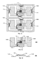
- FIG. 2A illustrates an example leadframe 200 that includes an integral heat dissipation element 210 .
- the leadframe 200 also includes openings 220 that serve to form pads 240 A, 240 B, 240 C, 240 D (collectively “ 240 ”) and conductor elements 235 A, 235 B, 235 C, 235 D (collectively “ 235 ”) for coupling these pads 240 to light emitting elements that will be situated at sites 230 A, 230 B (collectively “ 230 ”) on the heat dissipating element 210 .
- the illustrated section of the leadframe comprises a pattern for producing two light emitting devices, each to be situated at site 230 A, 230 B on the heat dissipating element 210 .
- the leadframe 200 also includes tiebars 215 that serve to (temporarily) attach the conductor elements 235 and pads 240 to the leadframe. Even though these tiebars 215 couple the conductors 235 and pads 240 to the heatsink 210 , the conductors 235 and pads 240 do not form part of the heatsink 210 , because upon removal of the tiebars 215 , the conductors 235 and pads 240 will be isolated from the heatsink 210 . (That is, the heatsink 210 includes the continuous area bounded by the tiebars 215 .)
- the heatsink 210 may be any of a variety of materials that provide efficient thermal transfer and dissipation.
- the leadframe 200 is a sheet of copper, between 0.1 mm and 0.4 mm thick. A thicker sheet is preferred for thermal transfer, but is more costly than a thinner sheet, and creating the openings 220 may be more difficult and/or more costly.
- FIG. 2B illustrates the leadframe 200 after being populated with light emitting elements 250 A, 250 B and protective structures 260 A, 260 B.
- both contacts of the light emitting elements 250 A, 250 B are situated on the top surface of each light emitting element 250 , and bonding wires 255 A, 255 B, 255 C, 255 D are used to couple the contacts of the light emitting elements 250 A, 250 B to the pads 240 A, 240 B, 240 C, 240 D.
- the protective structures 260 A, 260 B encompasses portions of the heat dissipating element 210 and conductors 235 , thereby fixing their position relative to each other, and providing structural support for the elements within the structures 260 A, 260 B.
- the structures 260 A, 260 B may be any of a number of forms.
- the structures 260 A, 260 B includes a transparent silicone material that is molded over the light emitting elements 250 A, 250 B on the heat dissipating element 210 .
- the silicone material may include a wavelength conversion material for producing a desired color of the emitted light.
- the structures 260 A, 260 B may be a reflective structure with an opening that accommodates the light emitting elements 250 A, 250 B.
- the structures 260 A, 260 B may comprise a material that has a high thermal dissipation efficiency, to further enhance the heat dissipation characteristics of the light emitting device.
- the tiebars 215 may be removed, typically via a metal punch process.
- the figures are provided to facilitate an understanding of the invention, and are not drawn to scale.
- the tiebars 215 may be substantially thinner than illustrated, to facilitate their removal by punching or other process intended to sever these tiebars 215 .
- FIG. 2C illustrates a singulated light emitting device 290 after the tiebars 215 are removed
- FIG. 2D illustrates the device 290 after the conductive elements 235 are formed to place the pads 240 lower than the structure 260 .
- This device 290 offers substantial benefits with regard to heat dissipation efficiency.
- the light emitting element 250 is mounted directly upon the heat dissipation element 210 .
- a thermally efficient bonding material such as silver filled epoxy, may be used to optimize the thermal transfer from the light emitting element 250 A to the heat dissipation element 210 .
- a portion of the heat dissipation element 210 in this example extends beyond the structure 260 A, providing for an efficient transfer of heat to the surrounding medium, which may be air, water, or other medium.
- the amount of heat dissipation provided by the heat dissipation element will be dependent upon the characteristics of the material used as the leadframe 200 , as well as the surface area of the heat dissipation element 210 .
- the size of the heat dissipation element 210 may vary, depending upon the amount of heat that the particular light emitting element 250 A is expected to generate. In some embodiments, the heat dissipation requirement may be such that the heat dissipation element need not extend beyond the extent of the structure 260 A; in other embodiments, the heat dissipation element may extend well beyond the extent of the structure 260 A. In this manner, high power light emitting elements 250 A may be accommodated using the same structure 260 A, conductors 235 A, 235 B, and pads 240 A, 240 B by merely increasing the size of the heat dissipation element 210 .
- the extent of the heat dissipation element 210 in one dimension is perpendicular to the lateral extent of the conductor elements 235 A, 235 B, the extent of the heat dissipation element 210 may be increased or decreased without requiring a modification to the architecture of the conductive elements 235 A, 235 B relative to the site of the light emitting element 250 .
- the area encompassed by the heat dissipation element 210 is at least 50% of the total area encompassed by the finished device 290 ; preferably the area of the heat dissipation element is at least 65% of the total area; and more preferably, the area of the heat dissipation element is at least 85% of the total area.
- the size of the heat dissipating element is sufficient to maintain the light emitting element 250 A at a non-damaging temperature during operation at nominal operating conditions.
- the size of the heat dissipating element 210 is sufficient to maintain the temperature of the light emitting element below 85° C. at 0.5 watt.
- additional heat dissipation may be achieved by appropriately shaping the heat dissipation element 210 after the structure 260 A is formed, and/or by coupling the heat dissipation element 210 to external heat dissipation elements, such as a set of heat dissipating tins, to provide additional heat dissipating surface area.
- the heat dissipation characteristics may be enhanced by using a material with high thermal dissipation efficiency to form the structure 260 A.
- the size of the heat dissipating element may be reduced accordingly to maintain the light emitting element 250 A within this structure 260 A at a non-damaging temperature.
- FIG. 3A illustrates a leadframe 300 for producing a light emitting structure that will include four light emitting elements, each situated at a site 330 on a heat dissipating element 310 .
- a single heat dissipating element 310 is common to all of the light emitting elements.
- the leadframe 300 includes openings 320 that serve to create different segments of the leadframe 300 , including the creation of the heat dissipating element 310 as defined by the continuous area between tiebars 315 .
- the openings 320 also create conductor elements 325 (illustrated in FIG. 3B ) that are separated from the heat dissipation element 310 by the tiebars 315 .
- FIG. 3B illustrates the leadframe 300 after being populated by light emitting elements 250 and structures 260 .
- the four light emitting elements 250 are connected in series between pads 340 A and 340 B, via the conductive elements 325 .
- FIG. 3C illustrates the removal of the tiebars 315 (illustrated in FIG. 3A ), as indicated by the “X” s that sever these tiebars, to provide a singulated light emitting structure 390 as illustrated in FIGS. 3D and 3E .
- the leads to the pads 340 A, 340 B may subsequently be formed to provide a desired profile.
- the light emitting structure 390 is illustrated as having four distinct protective structures 260 , one of skill in the art will recognize that a single protective structure could extend across all four of the light emitting elements 250 .
- the heat dissipating element 310 of light emitting structure 290 may be sized to provide sufficient heat dissipation for the particular light emitting elements 250 within the light emitting structure 390 .
- the embodiment of a light emitting structure that includes multiple light emitting devices with integral heat dissipation elements) offers potential for creating structures that provide a desired light output pattern.
- FIG. 4A illustrates a leadframe 400 that provides a light emitting structure that includes eight light emitting elements, each with an integral heat dissipation element 410 .
- the light emitting structure is intended to be formed so as to emit light in all radial directions of a circle, as illustrated in FIG. 4E .
- the leadframe 400 includes heat dissipation elements 410 and conductor elements 435 that extend between sites 430 upon which the light emitting elements will be situated. Tiebars 415 enable the conductor elements 435 to be separated from the heat dissipation element 410 .
- the conductor elements 435 include three conductors that are coupled by elements 426 . The use of three thin conductors to form conductor element 435 facilitate the bending of the structure at the regions 420 between the heat dissipation elements 410 , as illustrated in FIG. 4E .
- the heat dissipation elements 410 are coupled to each other for structural stability, also using thin elements 428 in the region 420 .
- the use of thin elements 428 also facilitates the aforementioned bending of the structure at the regions 420 between the heat dissipation elements 410 .
- the use of multiple thin elements in the conductor element 435 also facilitate the forming of alternative circuit configurations.
- the coupling 436 between the multiple elements forming the conductor element 435 may be severed to provide multiple conductor paths between and among the light emitting elements 250 .
- Such paths may allow for a parallel arrangement of the light emitting elements 250 , or for a structure that couples the elements in a selective manner depending upon a desired output luminance level, or a desired output pattern.
- the upper separated conductor elements 435 A could be coupled to a positive voltage
- the lower separated conductor elements 435 C could be coupled to a negative voltage, or ground.
- the bonding wire 455 A that attach to the contacts of the light emitting elements 250 A would be ‘stitched’ to couple the “p-contact” to the upper conductor element 435 A to the left and right of the light emitting element 250 A
- the bonding wire 455 B would couple the “n-contact” to the lower conductor element 435 C to the left and right of the light emitting element 250 .
- Light emitting element 250 B would be similarly connected to 435 A and 435 C. In this manner, the light emitting elements 250 A, 250 B would be connected in parallel.
- the center conductor element 435 B could be used to selectively arrange a series arrangement of light emitting elements 250 C, 250 D to be placed in parallel with the parallel arrangement of light emitting elements 250 A and 250 B.
- the corresponding circuit diagram is illustrated in FIG. 4C .
- the coupling 436 of FIG. 4A will serve as a tie-bar to hold the individual conductor elements 435 A, 435 B, 435 C in place until the protective structures 460 are formed, then severed.
- each heat dissipation element 410 is approximately 7 mm
- the space 420 is approximately 2 mm
- the protective structure 460 is approximately 6 mm ⁇ 6 mm
- the opening 465 is approximately 1.5 mm ⁇ 2.5 mm
- the light emitting element is approximately 1 mm ⁇ 1 mm.
- the heat dissipation element 410 comprises about 75% of the total area encompassed by the light emitting structure of 490 illustrated in FIGS. 4D-4E .
- the protective structure 460 may be a reflective enclosure that surrounds the light emitting element 250 .
- the structure 460 may be formed on the leadframe 400 before the light emitting element 250 is bonded to the heat dissipating element 410 , to avoid subjecting the light emitting element 250 to the process used to form the structure 460 .
- the structure 460 includes an opening 465 that is sufficient to enable the placement and bonding of the light emitting element 250 to the heat dissipation element 410 , and the wirebonding of the light emitting element 250 to the conductor elements 435 .
- An encapsulant (not illustrated) may be used to fill the opening 465 in the structure 460 , and this encapsulant may include a wavelength conversion material.
- the protective structure 460 may comprise a material with high emissivity.
- connection of the light emitting elements 250 to an external source of power may be effected by coupling to the exposed conductor elements 435 at each end of the arrangement of light emitting elements 250 .
- FIG. 4D illustrates a fully populated light emitting structure 490 comprising eight light emitting elements 250 , supporting structures 430 , conductive elements 435 , and individual heat dissipation elements/panels 410 .
- the heat dissipation panels 410 extend along a first axis 470 relative to the supporting structures 430
- the conductor elements 435 extend along a second axis 480 that is substantially orthogonal to the first axis 470 .
- the heat dissipation panels 410 can be extended or contracted, depending upon the heat dissipation requirements, while maintaining the same arrangement of conductor elements 435 , and vice versa.
- FIG. 4E illustrates the structure 490 formed in a somewhat circular form to provide light emission in all radial directions relative to a circle centered on the structure 490 .
- the eight heat dissipating panels 410 are coupled together via the thin elements 428 and 435 that are bent to form the eight panels 410 into an 8-sided shape, with each of the light emitting elements 250 illuminating an arc of at least 45°, thereby providing a illumination arc of 360° (8*45).
- fewer, or more panels 410 may be included, depending upon the desired uniformity of the light over the illumination arc, with additional panels 410 serving to enhance the uniformity.
- FIG. 5 illustrates an example flow diagram for manufacturing light emitting structures with integral heat dissipation elements.
- the leadframe is formed by creating openings in a metal substrate, such as a copper strip or plate, to form heat dissipation elements with sites for mounting light emitting elements and conductive elements for coupling the light emitting elements to external power sources.
- the conductive elements may be coupled to the heat dissipation elements via removable tiebars.
- reflective structures may be formed around the sites of the light emitting elements, with an opening that permits the placement of the light emitting element at the site and the coupling of the light emitting elements to the conductive elements.
- the light emitting elements are bonded to the heat dissipating element, preferably using a bonding material having high thermal transfer efficiency.
- the contacts of the light emitting elements are coupled to the conductive elements. Wire bonding may be used to provide this coupling.
- the light emitting element is encapsulated with a transparent protective material, such as silicone.
- the protective material may include wavelength conversion material, such as a phosphor that absorbs some or all of the light of the wavelength emitted by the light emitting element and emits light at a different wavelength.
- the tiebars that coupled the conductive elements to the heat dissipation element are removed, as are the tiebars that coupled each of the individual structures, thereby singulating the individual light emitting structures, as in the example of FIG. 2D , or singulating groups of light emitting structures, as in the example of FIGS. 3D and 4D .
- the portion of the leadframe that is external to the protective structure(s) surrounding the light emitting element(s) may be formed into a desired shape that facilitates the use of the light emitting structure in a higher assembly.
- each of the heat dissipation elements may differ in size, depending upon the heat generated by the particular type of device situated on each heat dissipation element, to maintain a relatively uniform temperature among all of the different types of light emitting elements.
- the heat dissipation element is isolated from each of the contacts of the light emitting elements.
- the heat dissipation element may form one of the pads that couple the external source to the light emitting element. That is, for example, one of the contacts of the light emitting element 250 of FIGS. 2B-2D may be electrically coupled to the heat dissipation element 210 , and a separate pad 240 B need not be formed, the external coupling to the light emitting element 250 being provided by pad 240 A and the heat dissipation element 210 .
- each light emitting element 250 may include multiple chips, for increased illumination, multiple wavelength illumination, and so on.
- the light emitting elements 250 and/or the protective elements 240 may include wavelength transforming material, such as a phosphor.
Landscapes
- Led Device Packages (AREA)
Abstract
Description
Claims (21)
Priority Applications (1)
| Application Number | Priority Date | Filing Date | Title |
|---|---|---|---|
| US15/538,048 US10340432B2 (en) | 2014-12-30 | 2015-12-30 | LED package with integrated features for gas or liquid cooling |
Applications Claiming Priority (3)
| Application Number | Priority Date | Filing Date | Title |
|---|---|---|---|
| US201462097623P | 2014-12-30 | 2014-12-30 | |
| US15/538,048 US10340432B2 (en) | 2014-12-30 | 2015-12-30 | LED package with integrated features for gas or liquid cooling |
| PCT/US2015/067973 WO2016109611A2 (en) | 2014-12-30 | 2015-12-30 | Led package with integrated features for gas or liquid cooling |
Related Parent Applications (1)
| Application Number | Title | Priority Date | Filing Date |
|---|---|---|---|
| PCT/US2015/067973 A-371-Of-International WO2016109611A2 (en) | 2014-12-30 | 2015-12-30 | Led package with integrated features for gas or liquid cooling |
Related Child Applications (1)
| Application Number | Title | Priority Date | Filing Date |
|---|---|---|---|
| US16/458,991 Continuation US11171273B2 (en) | 2014-12-30 | 2019-07-01 | LED package with integrated features for gas or liquid cooling |
Publications (2)
| Publication Number | Publication Date |
|---|---|
| US20170373237A1 US20170373237A1 (en) | 2017-12-28 |
| US10340432B2 true US10340432B2 (en) | 2019-07-02 |
Family
ID=55168457
Family Applications (2)
| Application Number | Title | Priority Date | Filing Date |
|---|---|---|---|
| US15/538,048 Active 2036-06-24 US10340432B2 (en) | 2014-12-30 | 2015-12-30 | LED package with integrated features for gas or liquid cooling |
| US16/458,991 Active 2036-03-02 US11171273B2 (en) | 2014-12-30 | 2019-07-01 | LED package with integrated features for gas or liquid cooling |
Family Applications After (1)
| Application Number | Title | Priority Date | Filing Date |
|---|---|---|---|
| US16/458,991 Active 2036-03-02 US11171273B2 (en) | 2014-12-30 | 2019-07-01 | LED package with integrated features for gas or liquid cooling |
Country Status (3)
| Country | Link |
|---|---|
| US (2) | US10340432B2 (en) |
| TW (2) | TWI767246B (en) |
| WO (1) | WO2016109611A2 (en) |
Families Citing this family (2)
| Publication number | Priority date | Publication date | Assignee | Title |
|---|---|---|---|---|
| WO2018108676A1 (en) * | 2016-12-13 | 2018-06-21 | Lumileds Holding B.V. | Arrangement of leds on a leadframe |
| CN219592702U (en) * | 2023-02-14 | 2023-08-25 | 隆达电子股份有限公司 | Light-emitting module and electrical module thereof |
Citations (9)
| Publication number | Priority date | Publication date | Assignee | Title |
|---|---|---|---|---|
| US20040180459A1 (en) | 2002-06-26 | 2004-09-16 | Cotco Holding Limited | LED package and the process making the same |
| WO2005101489A2 (en) | 2004-04-16 | 2005-10-27 | Lucea Ag | Housing for led chip and light source |
| JP2007096236A (en) | 2005-09-30 | 2007-04-12 | Toyoda Gosei Co Ltd | Led light emitting device |
| WO2009141960A1 (en) | 2008-05-20 | 2009-11-26 | Panasonic Corporation | Semiconductor light-emitting device as well as light source device and lighting system including the same |
| US20110156083A1 (en) * | 2009-12-30 | 2011-06-30 | Harvatek Corporation | Light emission module with high-efficiency light emission and high-efficiency heat dissipation and applications thereof |
| US20110303941A1 (en) | 2010-08-09 | 2011-12-15 | Lg Innotek Co., Ltd. | Light emitting device and lighting system |
| KR20130017461A (en) | 2011-08-10 | 2013-02-20 | 엘지이노텍 주식회사 | The light emitting device package and the light emitting system |
| WO2014016734A1 (en) | 2012-07-24 | 2014-01-30 | Koninklijke Philips N.V. | Matrix leadframe for led packaging |
| US9722157B2 (en) * | 2010-04-09 | 2017-08-01 | Rohm Co., Ltd. | LED module |
Family Cites Families (3)
| Publication number | Priority date | Publication date | Assignee | Title |
|---|---|---|---|---|
| TW201011936A (en) * | 2008-09-05 | 2010-03-16 | Advanced Optoelectronic Tech | Light emitting device and fabrication thereof |
| US8269244B2 (en) * | 2010-06-28 | 2012-09-18 | Cree, Inc. | LED package with efficient, isolated thermal path |
| JP5869976B2 (en) | 2012-07-25 | 2016-02-24 | Jx金属株式会社 | Method for producing metal-liquid crystal polymer composite |
-
2015
- 2015-12-30 TW TW109118484A patent/TWI767246B/en active
- 2015-12-30 US US15/538,048 patent/US10340432B2/en active Active
- 2015-12-30 WO PCT/US2015/067973 patent/WO2016109611A2/en not_active Ceased
- 2015-12-30 TW TW104144525A patent/TWI698033B/en active
-
2019
- 2019-07-01 US US16/458,991 patent/US11171273B2/en active Active
Patent Citations (9)
| Publication number | Priority date | Publication date | Assignee | Title |
|---|---|---|---|---|
| US20040180459A1 (en) | 2002-06-26 | 2004-09-16 | Cotco Holding Limited | LED package and the process making the same |
| WO2005101489A2 (en) | 2004-04-16 | 2005-10-27 | Lucea Ag | Housing for led chip and light source |
| JP2007096236A (en) | 2005-09-30 | 2007-04-12 | Toyoda Gosei Co Ltd | Led light emitting device |
| WO2009141960A1 (en) | 2008-05-20 | 2009-11-26 | Panasonic Corporation | Semiconductor light-emitting device as well as light source device and lighting system including the same |
| US20110156083A1 (en) * | 2009-12-30 | 2011-06-30 | Harvatek Corporation | Light emission module with high-efficiency light emission and high-efficiency heat dissipation and applications thereof |
| US9722157B2 (en) * | 2010-04-09 | 2017-08-01 | Rohm Co., Ltd. | LED module |
| US20110303941A1 (en) | 2010-08-09 | 2011-12-15 | Lg Innotek Co., Ltd. | Light emitting device and lighting system |
| KR20130017461A (en) | 2011-08-10 | 2013-02-20 | 엘지이노텍 주식회사 | The light emitting device package and the light emitting system |
| WO2014016734A1 (en) | 2012-07-24 | 2014-01-30 | Koninklijke Philips N.V. | Matrix leadframe for led packaging |
Non-Patent Citations (1)
| Title |
|---|
| EPO as ISA, "International Search Report and Written Opinion" dated Jun. 28, 2016 from International Application No. PCT/US2015/067973, filed Dec. 30, 2015, 17 pages. |
Also Published As
| Publication number | Publication date |
|---|---|
| US20170373237A1 (en) | 2017-12-28 |
| WO2016109611A3 (en) | 2016-08-25 |
| TWI767246B (en) | 2022-06-11 |
| US20200119246A1 (en) | 2020-04-16 |
| TW202040844A (en) | 2020-11-01 |
| TW201635602A (en) | 2016-10-01 |
| US11171273B2 (en) | 2021-11-09 |
| WO2016109611A2 (en) | 2016-07-07 |
| TWI698033B (en) | 2020-07-01 |
Similar Documents
| Publication | Publication Date | Title |
|---|---|---|
| TWI395345B (en) | LED lamp with low thermal resistance | |
| KR101488451B1 (en) | Multichip LED package | |
| TWI505519B (en) | Light-emitting diode light bar and manufacturing method thereof | |
| US20090289274A1 (en) | Package structure of light emitting diode and method of manufacturing the same | |
| JP3770192B2 (en) | Chip-type LED lead frame | |
| US20140103505A1 (en) | Die down integrated circuit package with integrated heat spreader and leads | |
| JP2013110298A (en) | Electronic component mounting package, electronic component package, and methods for manufacturing the same | |
| JP2012124248A (en) | Lead frame substrate for mounting led chip, method for manufacturing the same and led package | |
| KR100937136B1 (en) | Light Emitting Diode Module Using Lead Frame Modulated Multiple Packages | |
| US11171273B2 (en) | LED package with integrated features for gas or liquid cooling | |
| KR20120085085A (en) | Cob type light emitting module and method of the light emitting module | |
| KR20080079745A (en) | Light emitting diode package base having double heat dissipation structure between lead frame and heat dissipation plate and manufacturing method | |
| CN102214587B (en) | Method for making multilayer array type light emitting diode | |
| CN201204209Y (en) | LED lead base | |
| US9887179B2 (en) | Light emitting diode device and light emitting device using the same | |
| CN103000783A (en) | Light emitting diode and manufacturing method thereof | |
| JP2012182297A (en) | Lead frame for led, led module, and manufacturing method thereof | |
| EP3410501B1 (en) | Light-emitting diode module and light apparatus | |
| US20150070881A1 (en) | Led light tube of module type | |
| CN101615644B (en) | Thin light-emitting diode and manufacturing method thereof | |
| KR100865487B1 (en) | Submount type LED package and manufacturing method thereof | |
| CN201247781Y (en) | Wire frame structure of thin type LED | |
| KR100979971B1 (en) | Method for manufacturing light emitting diode unit, and light emitting diode unit manufactured by this method | |
| KR100600856B1 (en) | Lead frame for high power LED package and manufacturing method thereof | |
| KR101916371B1 (en) | Led package set and led bulb including the same |
Legal Events
| Date | Code | Title | Description |
|---|---|---|---|
| AS | Assignment |
Owner name: KONINKLIJKE PHILIPS N.V., NETHERLANDS Free format text: ASSIGNMENT OF ASSIGNORS INTEREST;ASSIGNORS:MEHNERT, AXEL;GOLUBOVIC, DUSAN;DONKER, MARCUS FRANCISCUS;AND OTHERS;SIGNING DATES FROM 20160118 TO 20160311;REEL/FRAME:042759/0246 |
|
| AS | Assignment |
Owner name: DEUTSCHE BANK AG NEW YORK BRANCH, AS COLLATERAL AGENT, NEW YORK Free format text: SECURITY INTEREST;ASSIGNOR:LUMILEDS LLC;REEL/FRAME:043108/0001 Effective date: 20170630 Owner name: DEUTSCHE BANK AG NEW YORK BRANCH, AS COLLATERAL AG Free format text: SECURITY INTEREST;ASSIGNOR:LUMILEDS LLC;REEL/FRAME:043108/0001 Effective date: 20170630 |
|
| AS | Assignment |
Owner name: LUMILEDS LLC, CALIFORNIA Free format text: ASSIGNMENT OF ASSIGNORS INTEREST;ASSIGNOR:KONINKLIJKE PHILIPS N.V.;REEL/FRAME:044792/0018 Effective date: 20170630 |
|
| STPP | Information on status: patent application and granting procedure in general |
Free format text: NOTICE OF ALLOWANCE MAILED -- APPLICATION RECEIVED IN OFFICE OF PUBLICATIONS |
|
| STPP | Information on status: patent application and granting procedure in general |
Free format text: PUBLICATIONS -- ISSUE FEE PAYMENT VERIFIED |
|
| STCF | Information on status: patent grant |
Free format text: PATENTED CASE |
|
| MAFP | Maintenance fee payment |
Free format text: PAYMENT OF MAINTENANCE FEE, 4TH YEAR, LARGE ENTITY (ORIGINAL EVENT CODE: M1551); ENTITY STATUS OF PATENT OWNER: LARGE ENTITY Year of fee payment: 4 |
|
| AS | Assignment |
Owner name: SOUND POINT AGENCY LLC, NEW YORK Free format text: SECURITY INTEREST;ASSIGNORS:LUMILEDS LLC;LUMILEDS HOLDING B.V.;REEL/FRAME:062299/0338 Effective date: 20221230 |
|
| AS | Assignment |
Owner name: LUMILEDS HOLDING B.V., NETHERLANDS Free format text: RELEASE BY SECURED PARTY;ASSIGNOR:SOUND POINT AGENCY LLC;REEL/FRAME:070046/0001 Effective date: 20240731 Owner name: LUMILEDS LLC, CALIFORNIA Free format text: RELEASE BY SECURED PARTY;ASSIGNOR:SOUND POINT AGENCY LLC;REEL/FRAME:070046/0001 Effective date: 20240731 Owner name: LUMILEDS LLC, CALIFORNIA Free format text: RELEASE OF SECURITY INTEREST;ASSIGNOR:SOUND POINT AGENCY LLC;REEL/FRAME:070046/0001 Effective date: 20240731 Owner name: LUMILEDS HOLDING B.V., NETHERLANDS Free format text: RELEASE OF SECURITY INTEREST;ASSIGNOR:SOUND POINT AGENCY LLC;REEL/FRAME:070046/0001 Effective date: 20240731 |
|
| AS | Assignment |
Owner name: LUMILEDS SINGAPORE PTE. LTD., SINGAPORE Free format text: ASSIGNMENT OF ASSIGNORS INTEREST;ASSIGNOR:LUMILEDS LLC;REEL/FRAME:071888/0086 Effective date: 20250708 |