US10326046B2 - Growth method of aluminum gallium nitride - Google Patents
Growth method of aluminum gallium nitride Download PDFInfo
- Publication number
- US10326046B2 US10326046B2 US15/255,429 US201615255429A US10326046B2 US 10326046 B2 US10326046 B2 US 10326046B2 US 201615255429 A US201615255429 A US 201615255429A US 10326046 B2 US10326046 B2 US 10326046B2
- Authority
- US
- United States
- Prior art keywords
- gallium nitride
- aluminum gallium
- temperature
- nitride layer
- substrate
- Prior art date
- Legal status (The legal status is an assumption and is not a legal conclusion. Google has not performed a legal analysis and makes no representation as to the accuracy of the status listed.)
- Active, expires
Links
- 229910002601 GaN Inorganic materials 0.000 title claims abstract description 83
- RNQKDQAVIXDKAG-UHFFFAOYSA-N aluminum gallium Chemical compound [Al].[Ga] RNQKDQAVIXDKAG-UHFFFAOYSA-N 0.000 title claims abstract description 83
- 238000000034 method Methods 0.000 title claims abstract description 30
- 239000000758 substrate Substances 0.000 claims abstract description 33
- PMHQVHHXPFUNSP-UHFFFAOYSA-M copper(1+);methylsulfanylmethane;bromide Chemical compound Br[Cu].CSC PMHQVHHXPFUNSP-UHFFFAOYSA-M 0.000 claims description 12
- 229910052782 aluminium Inorganic materials 0.000 description 4
- XAGFODPZIPBFFR-UHFFFAOYSA-N aluminium Chemical compound [Al] XAGFODPZIPBFFR-UHFFFAOYSA-N 0.000 description 4
- TWNQGVIAIRXVLR-UHFFFAOYSA-N oxo(oxoalumanyloxy)alumane Chemical compound O=[Al]O[Al]=O TWNQGVIAIRXVLR-UHFFFAOYSA-N 0.000 description 4
- PIGFYZPCRLYGLF-UHFFFAOYSA-N Aluminum nitride Chemical compound [Al]#N PIGFYZPCRLYGLF-UHFFFAOYSA-N 0.000 description 3
- 230000015572 biosynthetic process Effects 0.000 description 3
- 230000007547 defect Effects 0.000 description 2
- XUIMIQQOPSSXEZ-UHFFFAOYSA-N Silicon Chemical compound [Si] XUIMIQQOPSSXEZ-UHFFFAOYSA-N 0.000 description 1
- 238000012986 modification Methods 0.000 description 1
- 230000004048 modification Effects 0.000 description 1
- 229910052710 silicon Inorganic materials 0.000 description 1
- 239000010703 silicon Substances 0.000 description 1
Images


Classifications
-
- H—ELECTRICITY
- H10—SEMICONDUCTOR DEVICES; ELECTRIC SOLID-STATE DEVICES NOT OTHERWISE PROVIDED FOR
- H10H—INORGANIC LIGHT-EMITTING SEMICONDUCTOR DEVICES HAVING POTENTIAL BARRIERS
- H10H20/00—Individual inorganic light-emitting semiconductor devices having potential barriers, e.g. light-emitting diodes [LED]
- H10H20/80—Constructional details
- H10H20/81—Bodies
- H10H20/8215—Bodies characterised by crystalline imperfections, e.g. dislocations; characterised by the distribution of dopants, e.g. delta-doping
-
- H01L33/025—
-
- C—CHEMISTRY; METALLURGY
- C30—CRYSTAL GROWTH
- C30B—SINGLE-CRYSTAL GROWTH; UNIDIRECTIONAL SOLIDIFICATION OF EUTECTIC MATERIAL OR UNIDIRECTIONAL DEMIXING OF EUTECTOID MATERIAL; REFINING BY ZONE-MELTING OF MATERIAL; PRODUCTION OF A HOMOGENEOUS POLYCRYSTALLINE MATERIAL WITH DEFINED STRUCTURE; SINGLE CRYSTALS OR HOMOGENEOUS POLYCRYSTALLINE MATERIAL WITH DEFINED STRUCTURE; AFTER-TREATMENT OF SINGLE CRYSTALS OR A HOMOGENEOUS POLYCRYSTALLINE MATERIAL WITH DEFINED STRUCTURE; APPARATUS THEREFOR
- C30B23/00—Single-crystal growth by condensing evaporated or sublimed materials
- C30B23/02—Epitaxial-layer growth
- C30B23/06—Heating of the deposition chamber, the substrate or the materials to be evaporated
- C30B23/063—Heating of the substrate
-
- C—CHEMISTRY; METALLURGY
- C30—CRYSTAL GROWTH
- C30B—SINGLE-CRYSTAL GROWTH; UNIDIRECTIONAL SOLIDIFICATION OF EUTECTIC MATERIAL OR UNIDIRECTIONAL DEMIXING OF EUTECTOID MATERIAL; REFINING BY ZONE-MELTING OF MATERIAL; PRODUCTION OF A HOMOGENEOUS POLYCRYSTALLINE MATERIAL WITH DEFINED STRUCTURE; SINGLE CRYSTALS OR HOMOGENEOUS POLYCRYSTALLINE MATERIAL WITH DEFINED STRUCTURE; AFTER-TREATMENT OF SINGLE CRYSTALS OR A HOMOGENEOUS POLYCRYSTALLINE MATERIAL WITH DEFINED STRUCTURE; APPARATUS THEREFOR
- C30B25/00—Single-crystal growth by chemical reaction of reactive gases, e.g. chemical vapour-deposition growth
- C30B25/02—Epitaxial-layer growth
- C30B25/10—Heating of the reaction chamber or the substrate
-
- C—CHEMISTRY; METALLURGY
- C30—CRYSTAL GROWTH
- C30B—SINGLE-CRYSTAL GROWTH; UNIDIRECTIONAL SOLIDIFICATION OF EUTECTIC MATERIAL OR UNIDIRECTIONAL DEMIXING OF EUTECTOID MATERIAL; REFINING BY ZONE-MELTING OF MATERIAL; PRODUCTION OF A HOMOGENEOUS POLYCRYSTALLINE MATERIAL WITH DEFINED STRUCTURE; SINGLE CRYSTALS OR HOMOGENEOUS POLYCRYSTALLINE MATERIAL WITH DEFINED STRUCTURE; AFTER-TREATMENT OF SINGLE CRYSTALS OR A HOMOGENEOUS POLYCRYSTALLINE MATERIAL WITH DEFINED STRUCTURE; APPARATUS THEREFOR
- C30B29/00—Single crystals or homogeneous polycrystalline material with defined structure characterised by the material or by their shape
- C30B29/10—Inorganic compounds or compositions
- C30B29/40—AIIIBV compounds wherein A is B, Al, Ga, In or Tl and B is N, P, As, Sb or Bi
- C30B29/403—AIII-nitrides
- C30B29/406—Gallium nitride
-
- H01L33/007—
-
- H01L33/0075—
-
- H01L33/32—
-
- H—ELECTRICITY
- H10—SEMICONDUCTOR DEVICES; ELECTRIC SOLID-STATE DEVICES NOT OTHERWISE PROVIDED FOR
- H10H—INORGANIC LIGHT-EMITTING SEMICONDUCTOR DEVICES HAVING POTENTIAL BARRIERS
- H10H20/00—Individual inorganic light-emitting semiconductor devices having potential barriers, e.g. light-emitting diodes [LED]
- H10H20/01—Manufacture or treatment
- H10H20/011—Manufacture or treatment of bodies, e.g. forming semiconductor layers
- H10H20/013—Manufacture or treatment of bodies, e.g. forming semiconductor layers having light-emitting regions comprising only Group III-V materials
- H10H20/0133—Manufacture or treatment of bodies, e.g. forming semiconductor layers having light-emitting regions comprising only Group III-V materials with a substrate not being Group III-V materials
- H10H20/01335—Manufacture or treatment of bodies, e.g. forming semiconductor layers having light-emitting regions comprising only Group III-V materials with a substrate not being Group III-V materials the light-emitting regions comprising nitride materials
-
- H—ELECTRICITY
- H10—SEMICONDUCTOR DEVICES; ELECTRIC SOLID-STATE DEVICES NOT OTHERWISE PROVIDED FOR
- H10H—INORGANIC LIGHT-EMITTING SEMICONDUCTOR DEVICES HAVING POTENTIAL BARRIERS
- H10H20/00—Individual inorganic light-emitting semiconductor devices having potential barriers, e.g. light-emitting diodes [LED]
- H10H20/01—Manufacture or treatment
- H10H20/011—Manufacture or treatment of bodies, e.g. forming semiconductor layers
- H10H20/013—Manufacture or treatment of bodies, e.g. forming semiconductor layers having light-emitting regions comprising only Group III-V materials
- H10H20/0137—Manufacture or treatment of bodies, e.g. forming semiconductor layers having light-emitting regions comprising only Group III-V materials the light-emitting regions comprising nitride materials
-
- H—ELECTRICITY
- H10—SEMICONDUCTOR DEVICES; ELECTRIC SOLID-STATE DEVICES NOT OTHERWISE PROVIDED FOR
- H10H—INORGANIC LIGHT-EMITTING SEMICONDUCTOR DEVICES HAVING POTENTIAL BARRIERS
- H10H20/00—Individual inorganic light-emitting semiconductor devices having potential barriers, e.g. light-emitting diodes [LED]
- H10H20/80—Constructional details
- H10H20/81—Bodies
- H10H20/822—Materials of the light-emitting regions
- H10H20/824—Materials of the light-emitting regions comprising only Group III-V materials, e.g. GaP
- H10H20/825—Materials of the light-emitting regions comprising only Group III-V materials, e.g. GaP containing nitrogen, e.g. GaN
Definitions
- the present invention relates to a growth method of aluminum gallium nitride, and more particularly to a growth method of n-type aluminum gallium nitride with a high aluminum content.
- FIG. 1 is an enlarged view showing the surface of n-type aluminum gallium nitride (Al 0.7 Ga 0.3 N) formed at a temperature of 1170° C.
- FIG. 2 is an enlarged view showing the surface of n-type aluminum gallium nitride (Al 0.7 Ga 0.3 N) formed at a temperature of 1060° C.
- n-type aluminum gallium nitride (Al 0.7 Ga 0.3 N) is formed at a higher temperature, there are fewer dark spots on its surface. Having a smoother surface improves the luminous efficiency when used in a light-emitting diode.
- experimental data FIG.
- n-type aluminum gallium nitride shows that forming n-type aluminum gallium nitride at higher temperatures leads to higher values for its sheet resistance. For instance, when n-type aluminum gallium nitride is formed at a temperature of 1170° C., the lowest value of sheet resistance is 180 (ohms/square); and at 1050° C., the lowest value of sheet resistance is 80 (ohms/square). When used in light-emitting diodes, a higher sheet resistance results in greater power consumption. Therefore, finding a way of forming n-type aluminum gallium nitride with fewer dark spots on its surface and with a low sheet resistance is desirable, in order to enhance the luminous efficiency and lower the power consumption when used in a light-emitting diode.
- the primary objective of the present invention is to provide a growth method of aluminum gallium nitride that reduces the number of dark spot defects present on the surface and also reduces its sheet resistance.
- the growth method of aluminum gallium nitride of the present invention includes the steps of: providing a substrate; forming a first aluminum gallium nitride layer on the substrate at a first temperature; and forming a second aluminum gallium nitride layer, on the first aluminum gallium nitride layer, at a second temperature.
- the first temperature is higher than the second temperature.
- the first temperature may be approximately 100° C. higher than the second temperature.
- the first temperature may be in the range of 1100° C. to 1200° C.
- the second temperature may be in the range of 1000° C. to 1100° C.
- the first aluminum gallium nitride layer may be a u-type aluminum gallium nitride layer or an n-type aluminum gallium nitride layer.
- the second aluminum gallium nitride layer may be an n-type aluminum gallium nitride layer.
- the n-type aluminum gallium nitride layer may be of composition Al y Ga 1-y N, wherein which y may be greater than 0.4.
- y may be equal to 0.7.
- the substrate may be an aluminum nitride substrate.
- the step of providing the substrate may include forming an aluminum nitride substrate on an aluminum oxide substrate.
- the n-type aluminum gallium nitride layer with high aluminum content formed by the method of the present invention has fewer dark spots on its surface. Thus the luminous efficiency is improved when used in a light-emitting diode.
- the n-type aluminum gallium nitride layer with high aluminum content formed by the method of the present invention has a lower value of sheet resistance. Thus power consumption is reduced when used in a light-emitting diode.
- FIG. 1 is a close-up view of the surface of n-type aluminum gallium nitride (Al 0.7 Ga 0.3 N) formed at a temperature of 1170° C.;
- FIG. 2 is a close-up view of the surface of n-type aluminum gallium nitride (Al 0.7 Ga 0.3 N) formed at a temperature of 1060° C.;
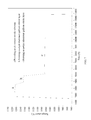
- FIG. 3 is a graph showing the relationship between silicon flow rate and sheet resistance, at different temperatures, for the growth of n-type aluminum gallium nitride (Al 0.7 Ga 0.3 N);
- FIG. 4 is a schematic view illustrating the layers formed following the growth method of aluminum gallium nitride according to the first embodiment of the present invention
- FIG. 5 is a flow chart showing the sequence of steps of the growth method of aluminum gallium nitride according to the first embodiment of the present invention
- FIG. 6 is a schematic view illustrating the layers formed following the growth method of aluminum gallium nitride according to the second embodiment of the present invention.
- FIG. 7 is a graph showing the progression in time of the temperature in the growth of aluminum gallium nitride according to the third embodiment of the present invention.
- FIG. 8 is a close-up view of the surface of aluminum gallium nitride according to the third embodiment of the present invention.
- One or more exemplary embodiments relate to a growth method of aluminum gallium nitride.
- the growth method of aluminum gallium nitride disclosed in the following embodiments can reduce the number of dark spot defects present on the surface of aluminum gallium nitride and also lower the value of its sheet resistance.
- a first embodiment of the present invention includes the formation of layers through a growth method of aluminum gallium nitride, wherein the substrate may consist of aluminum nitride (AlN).
- AlN aluminum nitride
- the schematic view of FIG. 4 illustrates the layers formed and the flow chart of FIG. 5 shows the sequence of steps in the growth method of aluminum gallium nitride according to the first embodiment of the present invention.
- the growth method of aluminum gallium nitride includes, in sequence, the step S 1 : providing a substrate, wherein the substrate may be an aluminum nitride (AlN) substrate 1 B; the step S 2 : forming a first aluminum gallium nitride layer 3 on the substrate at a first temperature, wherein, for example, in this embodiment the first temperature is around 1170° C.; and the step S 3 : forming a second aluminum gallium nitride layer 4 on the first aluminum gallium nitride layer 3 at a second temperature, wherein, for example, in this embodiment the second temperature is around 1060° C.
- the first and second temperatures of the present invention are not limited to the aforementioned values.
- Pertinent to the present invention is that the first temperature is higher than the second temperature.
- the first aluminum gallium nitride layer 3 is formed on the aluminum nitride substrate 1 B at the higher first temperature, and then the second aluminum gallium nitride layer 4 is formed on the first aluminum gallium nitride layer 3 at the lower second temperature to decrease the dark spots existed on the surface of aluminum gallium nitride and to lower the value of sheet resistance of aluminum gallium nitride.
- a second embodiment of the present invention also includes the formation of layers through a growth method of aluminum gallium nitride, wherein the substrate may consist of an aluminum oxide substrate and an aluminum nitride substrate.
- the schematic view of FIG. 6 illustrates the layers formed in the growth method of aluminum gallium nitride according to the second embodiment of the present invention.
- the substrate 1 is an aluminum nitride (AlN) template substrate composed of an aluminum oxide substrate 1 A and an aluminum nitride substrate 1 B formed on the aluminum oxide substrate 1 A.
- AlN aluminum nitride
- the first aluminum gallium nitride layer 3 of the present invention may be formed on the aluminum nitride substrate 1 B or the AlN template substrate 1 at the first temperature, for example at around 1170° C.
- the second aluminum gallium nitride layer 4 is formed on the first aluminum gallium nitride layer 3 at the second temperature, for example at around 1060° C.
- the first and second temperatures of the present invention are not limited to the aforementioned values. Pertinent to the present invention, as in the first embodiment, is that the first temperature is around 100° C. higher than the second temperature.
- the first aluminum gallium nitride layer 3 is first formed on the aluminum nitride substrate 1 B or the AlN template substrate 1 at the higher first temperature, and then the second aluminum gallium nitride layer 4 is formed on the first aluminum gallium nitride layer 3 at the lower second temperature, to form an aluminum gallium nitride layer with fewer dark spots on its surface and with a lower value of sheet resistance.
- a third embodiment of the present invention includes the formation of layers through a growth method of aluminum gallium nitride, wherein the first aluminum gallium nitride layer may consist of u-type or n-type aluminum gallium nitride and the second aluminum gallium nitride layer may consist of n-type aluminum gallium nitride with the composition Al 0.7 Ga 0.3 N.
- the graph of FIG. 7 shows the progression in time of the temperature in the growth of aluminum gallium nitride according to the third embodiment of the present invention.
- firstly an AlN substrate 1 B is provided, then the first aluminum gallium nitride layer 3 is formed on the AlN substrate 1 B at the first temperature of about 1170° C.
- first aluminum gallium nitride layer 3 of this embodiment consists of u-type aluminum gallium nitride, or may consist of n-type aluminum gallium nitride.
- the second aluminum gallium nitride layer 4 is formed on the u-type aluminum gallium nitride layer at the second temperature of around 1060° C.
- the second aluminum gallium nitride layer 4 of this embodiment consists of n-type aluminum gallium nitride of composition Al y Ga 1-y N, with the value of y being 0.7.
- the present invention is, however, not limited thereto; indeed a value greater than 0.4 for y is pertinent to the present invention.
- the first and the second temperatures of the present invention are also not limited to the aforementioned values.
- Pertinent to the present invention are a first temperature in the range of 1100° C. to 1200° C. and a second temperature in the range of 1000° C. to 1100° C. This results in fewer dark spots on the surface (as shown in FIG. 8 ) and a lower value of sheet resistance of the n-type aluminum gallium nitride layer with high aluminum content. Consequently, light-emitting diodes manufactured with the method of the present invention will have higher luminous efficiency and lower power consumption.
- a u- or n-type aluminum gallium nitride layer is first formed at a relatively high temperature, and then an n-type aluminum gallium nitride layer is formed at a relatively low temperature to form an n-type aluminum gallium nitride layer with fewer dark spots on its surface and with a lower value of sheet resistance.
- light-emitting diodes manufactured with the method of the present invention will have higher luminous efficiency and lower power consumption.
Landscapes
- Chemical & Material Sciences (AREA)
- Engineering & Computer Science (AREA)
- Crystallography & Structural Chemistry (AREA)
- Materials Engineering (AREA)
- Metallurgy (AREA)
- Organic Chemistry (AREA)
- Inorganic Chemistry (AREA)
- Chemical Kinetics & Catalysis (AREA)
- General Chemical & Material Sciences (AREA)
- Chemical Vapour Deposition (AREA)
- Led Devices (AREA)
Abstract
Description
Claims (7)
Applications Claiming Priority (3)
| Application Number | Priority Date | Filing Date | Title |
|---|---|---|---|
| TW105116898A | 2016-05-30 | ||
| TW105116898A TWI577842B (en) | 2016-05-30 | 2016-05-30 | Method for growing aluminum gallium nitride |
| TW105116898 | 2016-05-30 |
Publications (2)
| Publication Number | Publication Date |
|---|---|
| US20170345967A1 US20170345967A1 (en) | 2017-11-30 |
| US10326046B2 true US10326046B2 (en) | 2019-06-18 |
Family
ID=59241015
Family Applications (1)
| Application Number | Title | Priority Date | Filing Date |
|---|---|---|---|
| US15/255,429 Active 2037-12-18 US10326046B2 (en) | 2016-05-30 | 2016-09-02 | Growth method of aluminum gallium nitride |
Country Status (2)
| Country | Link |
|---|---|
| US (1) | US10326046B2 (en) |
| TW (1) | TWI577842B (en) |
Families Citing this family (1)
| Publication number | Priority date | Publication date | Assignee | Title |
|---|---|---|---|---|
| CN110643934A (en) * | 2019-09-20 | 2020-01-03 | 深圳市晶相技术有限公司 | Semiconductor device |
Citations (7)
| Publication number | Priority date | Publication date | Assignee | Title |
|---|---|---|---|---|
| US20060108603A1 (en) * | 2004-10-08 | 2006-05-25 | Toyoda Gosei Co., Ltd. | Group III nitride compound semiconductor light emitting device |
| US20090014839A1 (en) * | 2006-02-09 | 2009-01-15 | Rohm Co., Ltd | Nitride-Based Semiconductor Device |
| US20090057688A1 (en) * | 2007-08-27 | 2009-03-05 | Riken | Optical semiconductor device and manufacturing method therefor |
| US20100133508A1 (en) * | 2001-05-30 | 2010-06-03 | Cree, Inc. | Group iii nitride based quantum well light emitting device structures with an indium containing capping structure |
| US20110147771A1 (en) * | 2009-12-18 | 2011-06-23 | Yong Tae Moon | Light emitting device, light emitting device package and lighting system |
| US20150041755A1 (en) * | 2013-08-09 | 2015-02-12 | Qingdao Jason Electric Co., Ltd. | Light-emitting device with improved light extraction efficiency |
| US20170005223A1 (en) * | 2014-02-17 | 2017-01-05 | Osram Opto Semiconductors Gmbh | Method for Producing an Optoelectronic Semiconductor Chip and Optoelectronic Semiconductor Chip |
Family Cites Families (2)
| Publication number | Priority date | Publication date | Assignee | Title |
|---|---|---|---|---|
| JP3955291B2 (en) * | 2004-07-13 | 2007-08-08 | 株式会社共立 | Muffler with catalyst for internal combustion engine |
| CN101603172A (en) * | 2008-06-10 | 2009-12-16 | 北京大学 | A method of growing AlN or AlGaN film |
-
2016
- 2016-05-30 TW TW105116898A patent/TWI577842B/en active
- 2016-09-02 US US15/255,429 patent/US10326046B2/en active Active
Patent Citations (7)
| Publication number | Priority date | Publication date | Assignee | Title |
|---|---|---|---|---|
| US20100133508A1 (en) * | 2001-05-30 | 2010-06-03 | Cree, Inc. | Group iii nitride based quantum well light emitting device structures with an indium containing capping structure |
| US20060108603A1 (en) * | 2004-10-08 | 2006-05-25 | Toyoda Gosei Co., Ltd. | Group III nitride compound semiconductor light emitting device |
| US20090014839A1 (en) * | 2006-02-09 | 2009-01-15 | Rohm Co., Ltd | Nitride-Based Semiconductor Device |
| US20090057688A1 (en) * | 2007-08-27 | 2009-03-05 | Riken | Optical semiconductor device and manufacturing method therefor |
| US20110147771A1 (en) * | 2009-12-18 | 2011-06-23 | Yong Tae Moon | Light emitting device, light emitting device package and lighting system |
| US20150041755A1 (en) * | 2013-08-09 | 2015-02-12 | Qingdao Jason Electric Co., Ltd. | Light-emitting device with improved light extraction efficiency |
| US20170005223A1 (en) * | 2014-02-17 | 2017-01-05 | Osram Opto Semiconductors Gmbh | Method for Producing an Optoelectronic Semiconductor Chip and Optoelectronic Semiconductor Chip |
Also Published As
| Publication number | Publication date |
|---|---|
| TWI577842B (en) | 2017-04-11 |
| TW201809380A (en) | 2018-03-16 |
| US20170345967A1 (en) | 2017-11-30 |
Similar Documents
| Publication | Publication Date | Title |
|---|---|---|
| CN106057989B (en) | A kind of production method of the epitaxial wafer of GaN base light emitting | |
| US20080038857A1 (en) | Method of manufacturing nitride-based semiconductor light-emitting device | |
| TWI445204B (en) | Light-emitting element with gradient content tunneling layer | |
| CN102576782B (en) | There is light-emitting diode and the manufacture method thereof in the intermediate layer of high dislocation density | |
| CN205488195U (en) | Semiconductor light emitting element | |
| CN106129207A (en) | Epitaxial wafer and preparation method of gallium nitride-based light-emitting diode | |
| CN106299048A (en) | A kind of low-dislocation-density and the LED epitaxial structure of residual stress | |
| CN105405939A (en) | Light-emitting diode and manufacturing method thereof | |
| US20190198708A1 (en) | Light emitting diode epitaxial wafer and method for manufacturing the same | |
| CN106057990A (en) | Method for manufacturing epitaxial wafer of GaN-based light emitting diode | |
| US10326046B2 (en) | Growth method of aluminum gallium nitride | |
| JP4339822B2 (en) | Light emitting device | |
| CN102569541A (en) | Manufacturing method of semiconductor luminous chip | |
| CN204668342U (en) | The LED epitaxial structure of low-dislocation-density and residual stress | |
| CN105405947B (en) | Novel light-emitting diode epitaxial wafer and preparation method thereof | |
| CN105185881B (en) | A kind of light emitting diode and preparation method thereof | |
| CN102738337B (en) | Light emitting diode and manufacturing method thereof | |
| CN105679907A (en) | High-brightness light emitting diode epitaxial wafer and preparation method therefor | |
| CN106356715A (en) | Semiconductor laser and preparation method thereof | |
| CN108807613A (en) | LED epitaxial structure and preparation method thereof | |
| CN104810446B (en) | A kind of GaN base light emitting epitaxial wafer and preparation method thereof | |
| CN104465897B (en) | The manufacture method of LED crystal particle | |
| US9741898B2 (en) | Semiconductor light emitting device | |
| CN105895761B (en) | A kind of GaN light emitting diode with peelable structure | |
| CN105206717B (en) | GaN base light emitting epitaxial wafer and preparation method thereof |
Legal Events
| Date | Code | Title | Description |
|---|---|---|---|
| AS | Assignment |
Owner name: EPILEDS TECHNOLOGIES, INC., TAIWAN Free format text: ASSIGNMENT OF ASSIGNORS INTEREST;ASSIGNORS:HSU, KUNG-HSIEH;HSU, MING-SEN;REEL/FRAME:039705/0938 Effective date: 20160728 |
|
| STPP | Information on status: patent application and granting procedure in general |
Free format text: NOTICE OF ALLOWANCE MAILED -- APPLICATION RECEIVED IN OFFICE OF PUBLICATIONS |
|
| STCF | Information on status: patent grant |
Free format text: PATENTED CASE |
|
| FEPP | Fee payment procedure |
Free format text: ENTITY STATUS SET TO SMALL (ORIGINAL EVENT CODE: SMAL); ENTITY STATUS OF PATENT OWNER: SMALL ENTITY |
|
| MAFP | Maintenance fee payment |
Free format text: PAYMENT OF MAINTENANCE FEE, 4TH YR, SMALL ENTITY (ORIGINAL EVENT CODE: M2551); ENTITY STATUS OF PATENT OWNER: SMALL ENTITY Year of fee payment: 4 |