US10319301B2 - OLED display device and manufacture method thereof - Google Patents
OLED display device and manufacture method thereof Download PDFInfo
- Publication number
- US10319301B2 US10319301B2 US15/505,105 US201615505105A US10319301B2 US 10319301 B2 US10319301 B2 US 10319301B2 US 201615505105 A US201615505105 A US 201615505105A US 10319301 B2 US10319301 B2 US 10319301B2
- Authority
- US
- United States
- Prior art keywords
- layer
- metal oxide
- transparent conductive
- conductive metal
- pedot
- Prior art date
- Legal status (The legal status is an assumption and is not a legal conclusion. Google has not performed a legal analysis and makes no representation as to the accuracy of the status listed.)
- Active, expires
Links
Images


Classifications
-
- G—PHYSICS
- G09—EDUCATION; CRYPTOGRAPHY; DISPLAY; ADVERTISING; SEALS
- G09G—ARRANGEMENTS OR CIRCUITS FOR CONTROL OF INDICATING DEVICES USING STATIC MEANS TO PRESENT VARIABLE INFORMATION
- G09G3/00—Control arrangements or circuits, of interest only in connection with visual indicators other than cathode-ray tubes
- G09G3/20—Control arrangements or circuits, of interest only in connection with visual indicators other than cathode-ray tubes for presentation of an assembly of a number of characters, e.g. a page, by composing the assembly by combination of individual elements arranged in a matrix no fixed position being assigned to or needed to be assigned to the individual characters or partial characters
- G09G3/22—Control arrangements or circuits, of interest only in connection with visual indicators other than cathode-ray tubes for presentation of an assembly of a number of characters, e.g. a page, by composing the assembly by combination of individual elements arranged in a matrix no fixed position being assigned to or needed to be assigned to the individual characters or partial characters using controlled light sources
- G09G3/30—Control arrangements or circuits, of interest only in connection with visual indicators other than cathode-ray tubes for presentation of an assembly of a number of characters, e.g. a page, by composing the assembly by combination of individual elements arranged in a matrix no fixed position being assigned to or needed to be assigned to the individual characters or partial characters using controlled light sources using electroluminescent panels
- G09G3/32—Control arrangements or circuits, of interest only in connection with visual indicators other than cathode-ray tubes for presentation of an assembly of a number of characters, e.g. a page, by composing the assembly by combination of individual elements arranged in a matrix no fixed position being assigned to or needed to be assigned to the individual characters or partial characters using controlled light sources using electroluminescent panels semiconductive, e.g. using light-emitting diodes [LED]
- G09G3/3208—Control arrangements or circuits, of interest only in connection with visual indicators other than cathode-ray tubes for presentation of an assembly of a number of characters, e.g. a page, by composing the assembly by combination of individual elements arranged in a matrix no fixed position being assigned to or needed to be assigned to the individual characters or partial characters using controlled light sources using electroluminescent panels semiconductive, e.g. using light-emitting diodes [LED] organic, e.g. using organic light-emitting diodes [OLED]
- G09G3/3225—Control arrangements or circuits, of interest only in connection with visual indicators other than cathode-ray tubes for presentation of an assembly of a number of characters, e.g. a page, by composing the assembly by combination of individual elements arranged in a matrix no fixed position being assigned to or needed to be assigned to the individual characters or partial characters using controlled light sources using electroluminescent panels semiconductive, e.g. using light-emitting diodes [LED] organic, e.g. using organic light-emitting diodes [OLED] using an active matrix
- G09G3/3233—Control arrangements or circuits, of interest only in connection with visual indicators other than cathode-ray tubes for presentation of an assembly of a number of characters, e.g. a page, by composing the assembly by combination of individual elements arranged in a matrix no fixed position being assigned to or needed to be assigned to the individual characters or partial characters using controlled light sources using electroluminescent panels semiconductive, e.g. using light-emitting diodes [LED] organic, e.g. using organic light-emitting diodes [OLED] using an active matrix with pixel circuitry controlling the current through the light-emitting element
- G09G3/3241—Control arrangements or circuits, of interest only in connection with visual indicators other than cathode-ray tubes for presentation of an assembly of a number of characters, e.g. a page, by composing the assembly by combination of individual elements arranged in a matrix no fixed position being assigned to or needed to be assigned to the individual characters or partial characters using controlled light sources using electroluminescent panels semiconductive, e.g. using light-emitting diodes [LED] organic, e.g. using organic light-emitting diodes [OLED] using an active matrix with pixel circuitry controlling the current through the light-emitting element the current through the light-emitting element being set using a data current provided by the data driver, e.g. by using a two-transistor current mirror
-
- H01L27/3211—
-
- H01L27/3216—
-
- H01L27/3218—
-
- H01L27/3246—
-
- H01L27/3279—
-
- H01L51/001—
-
- H01L51/5212—
-
- H01L51/5215—
-
- H01L51/5228—
-
- H01L51/56—
-
- H—ELECTRICITY
- H10—SEMICONDUCTOR DEVICES; ELECTRIC SOLID-STATE DEVICES NOT OTHERWISE PROVIDED FOR
- H10K—ORGANIC ELECTRIC SOLID-STATE DEVICES
- H10K50/00—Organic light-emitting devices
- H10K50/10—OLEDs or polymer light-emitting diodes [PLED]
- H10K50/11—OLEDs or polymer light-emitting diodes [PLED] characterised by the electroluminescent [EL] layers
- H10K50/125—OLEDs or polymer light-emitting diodes [PLED] characterised by the electroluminescent [EL] layers specially adapted for multicolour light emission, e.g. for emitting white light
- H10K50/13—OLEDs or polymer light-emitting diodes [PLED] characterised by the electroluminescent [EL] layers specially adapted for multicolour light emission, e.g. for emitting white light comprising stacked EL layers within one EL unit
-
- H—ELECTRICITY
- H10—SEMICONDUCTOR DEVICES; ELECTRIC SOLID-STATE DEVICES NOT OTHERWISE PROVIDED FOR
- H10K—ORGANIC ELECTRIC SOLID-STATE DEVICES
- H10K50/00—Organic light-emitting devices
- H10K50/80—Constructional details
- H10K50/805—Electrodes
- H10K50/81—Anodes
- H10K50/814—Anodes combined with auxiliary electrodes, e.g. ITO layer combined with metal lines
-
- H—ELECTRICITY
- H10—SEMICONDUCTOR DEVICES; ELECTRIC SOLID-STATE DEVICES NOT OTHERWISE PROVIDED FOR
- H10K—ORGANIC ELECTRIC SOLID-STATE DEVICES
- H10K50/00—Organic light-emitting devices
- H10K50/80—Constructional details
- H10K50/805—Electrodes
- H10K50/81—Anodes
- H10K50/816—Multilayers, e.g. transparent multilayers
-
- H—ELECTRICITY
- H10—SEMICONDUCTOR DEVICES; ELECTRIC SOLID-STATE DEVICES NOT OTHERWISE PROVIDED FOR
- H10K—ORGANIC ELECTRIC SOLID-STATE DEVICES
- H10K50/00—Organic light-emitting devices
- H10K50/80—Constructional details
- H10K50/805—Electrodes
- H10K50/81—Anodes
- H10K50/818—Reflective anodes, e.g. ITO combined with thick metallic layers
-
- H—ELECTRICITY
- H10—SEMICONDUCTOR DEVICES; ELECTRIC SOLID-STATE DEVICES NOT OTHERWISE PROVIDED FOR
- H10K—ORGANIC ELECTRIC SOLID-STATE DEVICES
- H10K50/00—Organic light-emitting devices
- H10K50/80—Constructional details
- H10K50/805—Electrodes
- H10K50/82—Cathodes
- H10K50/824—Cathodes combined with auxiliary electrodes
-
- H—ELECTRICITY
- H10—SEMICONDUCTOR DEVICES; ELECTRIC SOLID-STATE DEVICES NOT OTHERWISE PROVIDED FOR
- H10K—ORGANIC ELECTRIC SOLID-STATE DEVICES
- H10K50/00—Organic light-emitting devices
- H10K50/80—Constructional details
- H10K50/85—Arrangements for extracting light from the devices
- H10K50/852—Arrangements for extracting light from the devices comprising a resonant cavity structure, e.g. Bragg reflector pair
-
- H—ELECTRICITY
- H10—SEMICONDUCTOR DEVICES; ELECTRIC SOLID-STATE DEVICES NOT OTHERWISE PROVIDED FOR
- H10K—ORGANIC ELECTRIC SOLID-STATE DEVICES
- H10K59/00—Integrated devices, or assemblies of multiple devices, comprising at least one organic light-emitting element covered by group H10K50/00
- H10K59/10—OLED displays
- H10K59/12—Active-matrix OLED [AMOLED] displays
- H10K59/122—Pixel-defining structures or layers, e.g. banks
-
- H—ELECTRICITY
- H10—SEMICONDUCTOR DEVICES; ELECTRIC SOLID-STATE DEVICES NOT OTHERWISE PROVIDED FOR
- H10K—ORGANIC ELECTRIC SOLID-STATE DEVICES
- H10K59/00—Integrated devices, or assemblies of multiple devices, comprising at least one organic light-emitting element covered by group H10K50/00
- H10K59/10—OLED displays
- H10K59/12—Active-matrix OLED [AMOLED] displays
- H10K59/131—Interconnections, e.g. wiring lines or terminals
- H10K59/1315—Interconnections, e.g. wiring lines or terminals comprising structures specially adapted for lowering the resistance
-
- H—ELECTRICITY
- H10—SEMICONDUCTOR DEVICES; ELECTRIC SOLID-STATE DEVICES NOT OTHERWISE PROVIDED FOR
- H10K—ORGANIC ELECTRIC SOLID-STATE DEVICES
- H10K59/00—Integrated devices, or assemblies of multiple devices, comprising at least one organic light-emitting element covered by group H10K50/00
- H10K59/30—Devices specially adapted for multicolour light emission
- H10K59/35—Devices specially adapted for multicolour light emission comprising red-green-blue [RGB] subpixels
- H10K59/352—Devices specially adapted for multicolour light emission comprising red-green-blue [RGB] subpixels the areas of the RGB subpixels being different
-
- H—ELECTRICITY
- H10—SEMICONDUCTOR DEVICES; ELECTRIC SOLID-STATE DEVICES NOT OTHERWISE PROVIDED FOR
- H10K—ORGANIC ELECTRIC SOLID-STATE DEVICES
- H10K59/00—Integrated devices, or assemblies of multiple devices, comprising at least one organic light-emitting element covered by group H10K50/00
- H10K59/30—Devices specially adapted for multicolour light emission
- H10K59/35—Devices specially adapted for multicolour light emission comprising red-green-blue [RGB] subpixels
- H10K59/353—Devices specially adapted for multicolour light emission comprising red-green-blue [RGB] subpixels characterised by the geometrical arrangement of the RGB subpixels
-
- H—ELECTRICITY
- H10—SEMICONDUCTOR DEVICES; ELECTRIC SOLID-STATE DEVICES NOT OTHERWISE PROVIDED FOR
- H10K—ORGANIC ELECTRIC SOLID-STATE DEVICES
- H10K71/00—Manufacture or treatment specially adapted for the organic devices covered by this subclass
-
- H—ELECTRICITY
- H10—SEMICONDUCTOR DEVICES; ELECTRIC SOLID-STATE DEVICES NOT OTHERWISE PROVIDED FOR
- H10K—ORGANIC ELECTRIC SOLID-STATE DEVICES
- H10K71/00—Manufacture or treatment specially adapted for the organic devices covered by this subclass
- H10K71/10—Deposition of organic active material
- H10K71/16—Deposition of organic active material using physical vapour deposition [PVD], e.g. vacuum deposition or sputtering
- H10K71/164—Deposition of organic active material using physical vapour deposition [PVD], e.g. vacuum deposition or sputtering using vacuum deposition
-
- H—ELECTRICITY
- H10—SEMICONDUCTOR DEVICES; ELECTRIC SOLID-STATE DEVICES NOT OTHERWISE PROVIDED FOR
- H10K—ORGANIC ELECTRIC SOLID-STATE DEVICES
- H10K2101/00—Properties of the organic materials covered by group H10K85/00
- H10K2101/10—Triplet emission
-
- H—ELECTRICITY
- H10—SEMICONDUCTOR DEVICES; ELECTRIC SOLID-STATE DEVICES NOT OTHERWISE PROVIDED FOR
- H10K—ORGANIC ELECTRIC SOLID-STATE DEVICES
- H10K2101/00—Properties of the organic materials covered by group H10K85/00
- H10K2101/40—Interrelation of parameters between multiple constituent active layers or sublayers, e.g. HOMO values in adjacent layers
-
- H—ELECTRICITY
- H10—SEMICONDUCTOR DEVICES; ELECTRIC SOLID-STATE DEVICES NOT OTHERWISE PROVIDED FOR
- H10K—ORGANIC ELECTRIC SOLID-STATE DEVICES
- H10K2102/00—Constructional details relating to the organic devices covered by this subclass
- H10K2102/301—Details of OLEDs
- H10K2102/351—Thickness
-
- H—ELECTRICITY
- H10—SEMICONDUCTOR DEVICES; ELECTRIC SOLID-STATE DEVICES NOT OTHERWISE PROVIDED FOR
- H10K—ORGANIC ELECTRIC SOLID-STATE DEVICES
- H10K85/00—Organic materials used in the body or electrodes of devices covered by this subclass
- H10K85/10—Organic polymers or oligomers
- H10K85/111—Organic polymers or oligomers comprising aromatic, heteroaromatic, or aryl chains, e.g. polyaniline, polyphenylene or polyphenylene vinylene
- H10K85/113—Heteroaromatic compounds comprising sulfur or selene, e.g. polythiophene
- H10K85/1135—Polyethylene dioxythiophene [PEDOT]; Derivatives thereof
-
- H—ELECTRICITY
- H10—SEMICONDUCTOR DEVICES; ELECTRIC SOLID-STATE DEVICES NOT OTHERWISE PROVIDED FOR
- H10K—ORGANIC ELECTRIC SOLID-STATE DEVICES
- H10K85/00—Organic materials used in the body or electrodes of devices covered by this subclass
- H10K85/30—Coordination compounds
- H10K85/341—Transition metal complexes, e.g. Ru(II)polypyridine complexes
- H10K85/342—Transition metal complexes, e.g. Ru(II)polypyridine complexes comprising iridium
-
- H—ELECTRICITY
- H10—SEMICONDUCTOR DEVICES; ELECTRIC SOLID-STATE DEVICES NOT OTHERWISE PROVIDED FOR
- H10K—ORGANIC ELECTRIC SOLID-STATE DEVICES
- H10K85/00—Organic materials used in the body or electrodes of devices covered by this subclass
- H10K85/60—Organic compounds having low molecular weight
- H10K85/631—Amine compounds having at least two aryl rest on at least one amine-nitrogen atom, e.g. triphenylamine
-
- H—ELECTRICITY
- H10—SEMICONDUCTOR DEVICES; ELECTRIC SOLID-STATE DEVICES NOT OTHERWISE PROVIDED FOR
- H10K—ORGANIC ELECTRIC SOLID-STATE DEVICES
- H10K85/00—Organic materials used in the body or electrodes of devices covered by this subclass
- H10K85/60—Organic compounds having low molecular weight
- H10K85/649—Aromatic compounds comprising a hetero atom
- H10K85/657—Polycyclic condensed heteroaromatic hydrocarbons
- H10K85/6572—Polycyclic condensed heteroaromatic hydrocarbons comprising only nitrogen in the heteroaromatic polycondensed ring system, e.g. phenanthroline or carbazole
Definitions
- the present invention relates to a display technology field, and more particularly to an OLED display device and a manufacture method thereof.
- the Organic Light Emitting Display (OLED) display which is also named as Organic electroluminescent display, is a new flat panel display device. Because it possesses many outstanding properties of self-illumination, low driving voltage, high luminescence efficiency, short response time, high clarity and contrast, near 180° view angle, wide range of working temperature, applicability of flexible display and large scale full color display.
- the OLED is considered as the most potential display device in the industry.
- the OLED display device possesses advantages of self-illumination, simple structure with low cost, fast response speed, wide view angle, high color saturation, high contrast, being light and flexible, more and more smart phones and the wearable devices start using the OLED display device.
- the OLED display element generally comprises a substrate, an anode located on the substrate, a Hole Injection Layer located on the anode, a Hole Transporting Layer located on the Hole Injection Layer, an emitting layer located on the Hole Transporting Layer, an Electron Transport Layer located on the emitting layer, an Electron Injection Layer located on the Electron Transport Layer and a Cathode located on the Electron Injection Layer.
- the principle of the OLED element is that the illumination generates due to the carrier injection and recombination under the electric field driving of the semiconductor material and the organic semiconductor illuminating material. Specifically, with a certain voltage driving, the Electron and the Hole are respectively injected into the Electron and Hole Transporting Layers from the cathode and the anode. The Electron and the Hole respectively migrate from the Electron and Hole Transporting Layers to the Emitting layer and bump into each other in the Emitting layer to form an exciton to excite the emitting molecule. The latter can illuminate after the radiative relaxation
- the full color display OLED display device generally comprises a plurality of red OLED elements, a plurality of green OLED elements, a plurality of blue OLED elements.
- the light emitting layers of the red OLED elements, the green OLED elements, the blue OLED elements respectively are red light emitting layers, green light emitting layers, blue light emitting layers.
- the hole transporting layers of the OLED elements of different colors are set to have different thicknesses to adjust the light distances of the red light, the green light, the blue light.
- the Fabry-Perot resonance principle is used to calculate the best light distances to make the red light emitting layers, green light emitting layers, blue light emitting layers respectively at the positions of the second antinodes, and thus, the luminous efficiencies reach the maximum. It requires that the hole transporting layers of the red OLED elements, the green OLED elements, the blue OLED elements need to use three different FMMs (Fine Metal Mask) to be manufactured with three evaporation processes. Accordingly, the production cost is increased, and the process time is extended. Meanwhile, the product yield decreases due to the complexity of the process.
- FMMs Feine Metal Mask
- An objective of the present invention is to provide an OLED display device, which can realize that the luminous efficiencies of the red OLED element, the green OLED element, the blue OLED element respectively achieve the best, and the production cost is low and the process is simple.
- Another objective of the present invention is to provide a manufacture method of an OLED display device, which can realize that the luminous efficiencies of the red OLED element, the green OLED element, the blue OLED element respectively achieve the best, and the production cost is low and the process is simple.
- the present invention provides an OLED display device, comprising a substrate, a pixel definition layer located on the substrate, a plurality of through holes located in the pixel definition layer, and a plurality of red OLED elements, a plurality of green OLED elements and a plurality of blue OLED elements, which are respectively located in the plurality of through holes;
- the red OLED element comprising a first transparent conductive metal oxide layer, a first metal layer, a first PEDOT:PSS conductive film layer, a second transparent conductive metal oxide layer, a first hole injection layer, a first hole transporting layer, a red light emitting layer, a first electron transporting layer and a first cathode on the substrate from bottom to top in order; the first transparent conductive metal oxide layer, the first metal layer, the first PEDOT:PSS conductive film layer and the second transparent conductive metal oxide layer constituting a first anode, together;
- the green OLED element comprising a third transparent conductive metal oxide layer, a second metal layer, a second PEDOT:PSS conductive film layer, a fourth transparent conductive metal oxide layer, a second hole injection layer, a second hole transporting layer, a green light emitting layer, a second electron transporting layer and a second cathode on the substrate from bottom to top in order; the third transparent conductive metal oxide layer, the second metal layer, the second PEDOT:PSS conductive film layer and the fourth transparent conductive metal oxide layer constituting a second anode, together;
- the blue OLED element comprising a fifth transparent conductive metal oxide layer, a third metal layer, a third PEDOT:PSS conductive film layer, a sixth transparent conductive metal oxide layer, a third hole injection layer, a third hole transporting layer, a blue light emitting layer, a third electron transporting layer and a third cathode on the substrate from bottom to top in order; the fifth transparent conductive metal oxide layer, the third metal layer, the third PEDOT:PSS conductive film layer and the sixth transparent conductive metal oxide layer constituting a third anode, together.
- Materials of the first PEDOT:PSS conductive film layer, the second PEDOT:PSS conductive film layer, the third PEDOT:PSS conductive film layer are the same, and a refractive index thereof is ⁇ P , and materials of the second transparent conductive metal oxide layer, the fourth transparent conductive metal oxide layer, the sixth transparent conductive metal oxide layer are the same, and a refractive index thereof is ⁇ I , and materials of the first hole injection layer, the second hole injection layer, the third hole injection layer are the same, and a refractive index thereof is ⁇ J , and materials of the first hole transporting layer, the second hole transporting layer, the third hole transporting layer are the same, and a refractive index thereof is ⁇ T , and a peak wavelength of red light emitted by the red light emitting layer is ⁇ R , and a peak wavelength of green light emitted by the green light emitting layer is ⁇ G , and a peak wavelength of blue light emitted by the blue light emitting layer is ⁇ B ;
- a thickness of the first PEDOT:PSS conductive film layer is defined to be d RP
- a thickness of the second transparent conductive metal oxide layer is defined to be d RI
- a thickness of the first hole injection layer is defined to be d RJ
- a thickness of the first hole transporting layer is defined to be d RT
- m R is a natural number
- a thickness of the second PEDOT:PSS conductive film layer is defined to be d GP
- a thickness of the fourth transparent conductive metal oxide layer is defined to be d GI
- a thickness of the second hole injection layer is defined to be d GJ
- a thickness of the second hole transporting layer is defined to be d GT
- m G is a natural number
- a thickness of the third PEDOT:PSS conductive film layer is defined to be d BP
- a thickness of the sixth transparent conductive metal oxide layer is defined to be d BI
- a thickness of the third hole injection layer is defined to be d BJ
- a thickness of the third hole transporting layer is defined to be d BT
- m B is a natural number
- ⁇ R , ⁇ G , ⁇ B are unequal, and thus, d RP , d GP , d BP are unequal.
- the plurality of through holes in the pixel definition layer appear to be tapered, and a dimension of the through hole gradually increases from one end away from the substrate to one end close to the substrate.
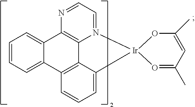
- the red light emitting layer comprises a main material and a doped dye, and the main material is CBP, and the doped dye is red phosphorescent dye, and the red phosphorescent dye is Ir(DBQ) 2 (acac);
- the green light emitting layer comprises a main material and a doped dye, and the main material is CBP, and the doped dye is green phosphorescent dye, and the green phosphorescent dye is Ir(ppy) 3 ;
- the blue light emitting layer comprises a main material and a doped dye, and the main material is AND, and the doped dye is blue fluorescent dye, and the blue fluorescent dye is BUBD-1;
- Materials of the first transparent conductive metal oxide layer, the second transparent conductive metal oxide layer, the third transparent conductive metal oxide layer, the fourth transparent conductive metal oxide layer, the fifth transparent conductive metal oxide layer, the sixth transparent conductive metal oxide layer are tin indium oxide, and materials of the first metal layer, the second metal layer, the third metal layer are silver;
- materials of the first cathode, the second cathode, the third cathode are the same, and comprise at least one of low work function metal, alloy formed by low work function metal and at least one of copper, gold, and silver, low work function metal nitride and low work function metal fluoride;
- the low work function metal comprises at least one of lithium, magnesium, calcium, strontium, aluminum and indium;
- materials of the first hole injection layer, the second hole injection layer, the third hole injection layer comprise HAT(CN) 6 , and a constitutional formula of HAT(CN) 6 is
- materials of the first electron transporting layer, the second electron transporting layer, the third electron transporting layer are the same, and comprise BPhen, and a constitutional formula of BPhen is
- the present invention further provides a manufacture method of an OLED display device, comprising steps of:
- step 1 providing a substrate, and forming a pixel definition layer on the substrate, and configuring a plurality of through holes which are separately located in the pixel definition layer, and the plurality of through holes defining a plurality of red pixel regions, a plurality of green pixel regions and a plurality of blue pixel regions on the substrate;
- PEDOT:PSS aqueous solution respectively coating PEDOT:PSS aqueous solution on the first metal layer, the second metal layer and the third metal layer, and forming a first PEDOT:PSS conductive film layer, a second PEDOT:PSS conductive film layer, a third PEDOT:PSS conductive film layer after curing and removing moisture;
- the first transparent conductive metal oxide layer, the first metal layer, the first PEDOT:PSS conductive film layer and the second transparent conductive metal oxide layer which are stacked up from bottom to top in order constituting a first anode, together;
- the third transparent conductive metal oxide layer, the second metal layer, the second PEDOT:PSS conductive film layer and the fourth transparent conductive metal oxide layer which are stacked up from bottom to top in order constituting a second anode, together;
- the fifth transparent conductive metal oxide layer, the third metal layer, the third PEDOT:PSS conductive film layer and the sixth transparent conductive metal oxide layer which are stacked up from bottom to top in order constituting a third anode, together;
- step 2 cleaning the first anode, the second anode and the third anode
- step 3 respectively evaporating a first hole injection layer, a second hole injection layer, a third hole injection layer on the first anode, the second anode and the third anode in the same evaporation process;
- red OLED elements green OLED elements and blue OLED elements respectively corresponding to the red pixel regions, the green pixel regions, the blue pixel regions in the plurality of through holes of the pixel definition layer.
- Materials of the first PEDOT:PSS conductive film layer, the second PEDOT:PSS conductive film layer, the third PEDOT:PSS conductive film layer are the same, and a refractive index thereof is ⁇ P , and materials of the second transparent conductive metal oxide layer, the fourth transparent conductive metal oxide layer, the sixth transparent conductive metal oxide layer are the same, and a refractive index thereof is ⁇ I , and materials of the first hole injection layer, the second hole injection layer, the third hole injection layer are the same, and a refractive index thereof is ⁇ J , and materials of the first hole transporting layer, the second hole transporting layer, the third hole transporting layer are the same, and a refractive index thereof is ⁇ T , and a peak wavelength of red light emitted by the red light emitting layer is ⁇ R , and a peak wavelength of green light emitted by the green light emitting layer is ⁇ G , and a peak wavelength of blue light emitted by the blue light emitting layer is ⁇ B ;
- a thickness of the first PEDOT:PSS conductive film layer is defined to be d RP
- a thickness of the second transparent conductive metal oxide layer is defined to be d RI
- a thickness of the first hole injection layer is defined to be d RJ
- a thickness of the first hole transporting layer is defined to be d RT
- m R is a natural number
- a thickness of the second PEDOT:PSS conductive film layer is defined to be d GP
- a thickness of the fourth transparent conductive metal oxide layer is defined to be d GI
- a thickness of the second hole injection layer is defined to be d GJ
- a thickness of the second hole transporting layer is defined to be d GT
- m G is a natural number
- a thickness of the third PEDOT:PSS conductive film layer is defined to be d BP
- a thickness of the sixth transparent conductive metal oxide layer is defined to be d BI
- a thickness of the third hole injection layer is defined to be d BJ
- a thickness of the third hole transporting layer is defined to be d BT
- m B is a natural number
- ⁇ R , ⁇ G , ⁇ B are unequal, and thus, d RP , d GP , d BP are unequal.
- the plurality of through holes in the pixel definition layer appear to be tapered, and a dimension of the through hole gradually increases from one end away from the substrate to one end close to the substrate.
- a magnetron sputtering method is used to deposit the first transparent conductive metal oxide layer, the second transparent conductive metal oxide layer, the third transparent conductive metal oxide layer, the fourth transparent conductive metal oxide layer, the fifth transparent conductive metal oxide layer, the sixth transparent conductive metal oxide layer, and the first metal layer, the second metal layer, the third metal layer are silver;
- an ink jet printing method is used to respectively coat PEDOT:PSS aqueous solution on the first metal layer, the second metal layer and the third metal layer.
- the red light emitting layer comprises a main material and a doped dye, and the main material is CBP, and the doped dye is red phosphorescent dye, and the red phosphorescent dye is Ir(DBQ) 2 (acac);
- the green light emitting layer comprises a main material and a doped dye, and the main material is CBP, and the doped dye is green phosphorescent dye, and the green phosphorescent dye is Ir(ppy) 3 ;
- the blue light emitting layer comprises a main material and a doped dye, and the main material is AND, and the doped dye is blue fluorescent dye, and the blue fluorescent dye is BUBD-1;
- the present invention further provides a manufacture method of an OLED display device, comprising steps of:
- step 1 providing a substrate, and forming a pixel definition layer on the substrate, and configuring a plurality of through holes which are separately located in the pixel definition layer, and the plurality of through holes defining a plurality of red pixel regions, a plurality of green pixel regions and a plurality of blue pixel regions on the substrate;
- PEDOT:PSS aqueous solution respectively coating PEDOT:PSS aqueous solution on the first metal layer, the second metal layer and the third metal layer, and forming a first PEDOT:PSS conductive film layer, a second PEDOT:PSS conductive film layer, a third PEDOT:PSS conductive film layer after curing and removing moisture;
- the first transparent conductive metal oxide layer, the first metal layer, the first PEDOT:PSS conductive film layer and the second transparent conductive metal oxide layer which are stacked up from bottom to top in order constituting a first anode, together;
- the third transparent conductive metal oxide layer, the second metal layer, the second PEDOT:PSS conductive film layer and the fourth transparent conductive metal oxide layer which are stacked up from bottom to top in order constituting a second anode, together;
- the fifth transparent conductive metal oxide layer, the third metal layer, the third PEDOT:PSS conductive film layer and the sixth transparent conductive metal oxide layer which are stacked up from bottom to top in order constituting a third anode, together;
- step 2 cleaning the first anode, the second anode and the third anode
- step 3 respectively evaporating a first hole injection layer, a second hole injection layer, a third hole injection layer on the first anode, the second anode and the third anode in the same evaporation process;
- red OLED elements green OLED elements and blue OLED elements respectively corresponding to the red pixel regions, the green pixel regions, the blue pixel regions in the plurality of through holes of the pixel definition layer;
- materials of the first PEDOT:PSS conductive film layer, the second PEDOT:PSS conductive film layer, the third PEDOT:PSS conductive film layer are the same, and a refractive index thereof is ⁇ P
- materials of the second transparent conductive metal oxide layer, the fourth transparent conductive metal oxide layer, the sixth transparent conductive metal oxide layer are the same, and a refractive index thereof is ⁇ I
- materials of the first hole injection layer, the second hole injection layer, the third hole injection layer are the same, and a refractive index thereof is ⁇ J
- materials of the first hole transporting layer, the second hole transporting layer, the third hole transporting layer are the same, and a refractive index thereof is ⁇ T
- a peak wavelength of red light emitted by the red light emitting layer is ⁇ R
- a peak wavelength of green light emitted by the green light emitting layer is ⁇ G
- a peak wavelength of blue light emitted by the blue light emitting layer is ⁇ B ;
- a thickness of the first PEDOT:PSS conductive film layer is defined to be d RP
- a thickness of the second transparent conductive metal oxide layer is defined to be d RI
- a thickness of the first hole injection layer is defined to be d RJ
- a thickness of the first hole transporting layer is defined to be d RT
- m R is a natural number
- a thickness of the second PEDOT:PSS conductive film layer is defined to be d GP
- a thickness of the fourth transparent conductive metal oxide layer is defined to be d GI
- a thickness of the second hole injection layer is defined to be d GJ
- a thickness of the second hole transporting layer is defined to be d GT
- m G is a natural number
- a thickness of the third PEDOT:PSS conductive film layer is defined to be d a p
- a thickness of the sixth transparent conductive metal oxide layer is defined to be d BI
- a thickness of the third hole injection layer is defined to be d BJ
- a thickness of the third hole transporting layer is defined to be d BT
- m B is a natural number
- ⁇ R , ⁇ G , ⁇ B are unequal, and thus, d RP , d GP , d BP are unequal;
- the plurality of through holes in the pixel definition layer appear to be tapered, and a dimension of the through hole gradually increases from one end away from the substrate to one end close to the substrate.
- the benefits of the present invention are: in the OLED display device and the manufacture method thereof provided by the present invention, by respectively configuring the first PEDOT:PSS conductive film layer, the second PEDOT:PSS conductive film layer, the third PEDOT:PSS conductive film layer in the red OLED element, the green OLED element, the blue OLED element, and setting the first PEDOT:PSS conductive film layer, the second PEDOT:PSS conductive film layer, the third PEDOT:PSS conductive film layer to have various thicknesses to realize that the luminous efficiencies of the red OLED element, the green OLED element, the blue OLED element respectively achieve the best, and all the first PEDOT:PSS conductive film layer, the second PEDOT:PSS conductive film layer, the third PEDOT:PSS conductive film layer are manufactured by the ink jet printing method, and the production cost is low and the process is simple.
- the thicknesses of the first hole transporting layer, the second hole transporting layer, the third hole transporting layer in the red OLED element, the green OLED element, the blue OLED element are the same in the OLED display device of the present invention, thus they can be formed in the same evaporation process with one common metal mask to eliminate three fine metal masks to lower the production cost and decrease the process time.
- FIG. 1 is a structure diagram of an OLED display device of the present invention
- FIG. 2 is a flowchart of a manufacture method of an OLED display device of the present invention.
- the present invention provides an OLED display device, comprising a substrate 10 , a pixel definition layer 20 located on the substrate 10 , a plurality of through holes 21 located in the pixel definition layer 20 , and a plurality of red OLED elements 30 , a plurality of green OLED elements 40 and a plurality of blue OLED elements 50 , which are respectively located in the plurality of through holes 21 ;
- the red OLED element 30 comprising a first transparent conductive metal oxide layer 31 , a first metal layer 32 , a first PEDOT:PSS conductive film layer 33 , a second transparent conductive metal oxide layer 34 , a first hole injection layer 35 , a first hole transporting layer 36 , a red light emitting layer 37 , a first electron transporting layer 38 and a first cathode 39 on the substrate 10 from bottom to top in order; the first transparent conductive metal oxide layer 31 , the first metal layer 32 , the first PEDOT:PSS conductive film layer 33 and the second transparent conductive metal oxide layer 34 constituting a first anode 301 , together;
- the green OLED element 40 comprising a third transparent conductive metal oxide layer 41 , a second metal layer 42 , a second PEDOT:PSS conductive film layer 43 , a fourth transparent conductive metal oxide layer 44 , a second hole injection layer 45 , a second hole transporting layer 46 , a green light emitting layer 47 , a second electron transporting layer 48 and a second cathode 49 on the substrate 10 from bottom to top in order; the third transparent conductive metal oxide layer 41 , the second metal layer 42 , the second PEDOT:PSS conductive film layer 43 and the fourth transparent conductive metal oxide layer 44 constituting a second anode 401 , together;
- the blue OLED element 50 comprising a fifth transparent conductive metal oxide layer 51 , a third metal layer 52 , a third PEDOT:PSS conductive film layer 53 , a sixth transparent conductive metal oxide layer 54 , a third hole injection layer 55 , a third hole transporting layer 56 , a blue light emitting layer 57 , a third electron transporting layer 58 and a third cathode 59 on the substrate 10 from bottom to top in order; the fifth transparent conductive metal oxide layer 51 , the third metal layer 52 , the third PEDOT:PSS conductive film layer 53 and the sixth transparent conductive metal oxide layer 54 constituting a third anode 501 , together.
- materials of the first PEDOT:PSS conductive film layer 33 , the second PEDOT:PSS conductive film layer 43 , the third PEDOT:PSS conductive film layer 53 are the same, and a refractive index thereof is ⁇ P
- materials of the second transparent conductive metal oxide layer 34 , the fourth transparent conductive metal oxide layer 44 , the sixth transparent conductive metal oxide layer 54 are the same, and a refractive index thereof is ⁇ I
- materials of the first hole injection layer 35 , the second hole injection layer 45 , the third hole injection layer 55 are the same, and a refractive index thereof is ⁇ J
- materials of the first hole transporting layer 36 , the second hole transporting layer 46 , the third hole transporting layer 56 are the same, and a refractive index thereof is ⁇ T
- a peak wavelength of red light emitted by the red light emitting layer 37 is ⁇ R
- a peak wavelength of green light emitted by the green light emitting layer 47 is ⁇ G
- a thickness of the first PEDOT:PSS conductive film layer 33 is defined to be d RP
- a thickness of the second transparent conductive metal oxide layer 34 is defined to be d RI
- a thickness of the first hole injection layer 35 is defined to be d RJ
- a thickness of the first hole transporting layer 36 is defined to be d RT
- m R is a natural number
- a thickness of the second PEDOT:PSS conductive film layer 43 is defined to be d GP
- a thickness of the fourth transparent conductive metal oxide layer 44 is defined to be d GI
- a thickness of the second hole injection layer 45 is defined to be d GJ
- a thickness of the second hole transporting layer 46 is defined to be d GT
- m G is a natural number
- a thickness of the third PEDOT:PSS conductive film layer 53 is defined to be d BP
- a thickness of the sixth transparent conductive metal oxide layer 54 is defined to be d BI
- a thickness of the third hole injection layer 55 is defined to be d BJ
- a thickness of the third hole transporting layer 56 is defined to be d BT
- m B is a natural number
- ⁇ R , ⁇ G , ⁇ B are unequal, and thus, d RP , d GP , d BP are unequal.
- the present invention adjusts the thicknesses of the first PEDOT:PSS conductive film layer 33 , the second PEDOT:PSS conductive film layer 43 , the third PEDOT:PSS conductive film layer 53 in the red OLED element 30 , the green OLED element 40 , the blue OLED element 50 to realize that the luminous efficiencies of the red OLED element 30 , the green OLED element 40 , the blue OLED element 50 respectively achieve the best, and all the first PEDOT:PSS conductive film layer 33 , the second PEDOT:PSS conductive film layer 43 , the third PEDOT:PSS conductive film layer 53 are manufactured by the ink jet printing method, and the production cost is low and the process is simple.
- the thicknesses of the first hole transporting layer 36 , the second hole transporting layer 46 , the third hole transporting layer 56 in the red OLED element 30 , the green OLED element 40 , the blue OLED element 50 are the same in the OLED display device of the present invention, thus they can be formed in the same evaporation process with one CMM (Common Metal Mask) to eliminate three fine metal masks to lower the production cost and decrease the process time.
- CMM Common Metal Mask
- all the first anode 301 , the second anode 302 , the third anode 303 are reflection electrodes, and all the first cathode 39 , the second cathode 49 , the third cathode 59 are semi transparent electrodes.
- all the red OLED element 30 , the green OLED element 40 , the blue OLED element 50 are top emitting OLED elements.
- the OLED element of the present invention is a top emitting OLED display device.
- the distance d from the light emitting layer to the reflection anode in the top emitting OLED element needs to satisfy the following relationship (4): [ ⁇ (2 m+ 1)/4 ⁇ (1 ⁇ 8)] ⁇ d ⁇ [ ⁇ (2 m+ 1)/4 ⁇ +(1 ⁇ 8)] ⁇ (4);
- d represents the distance from the light emitting layer to the reflection anode
- ⁇ represents the refractive index of the material between the light emitting layer and the reflection anode
- ⁇ represents the peak wavelength of the light emitted by the light emitting layer
- m represents the natural number
- the distance d satisfies the following relationship (5): [ ⁇ (2 m+ 1)/4 ⁇ ( 1/16)] ⁇ d ⁇ [ ⁇ (2 m+ 1)/4 ⁇ +( 1/16)] ⁇ (5);
- the distance d (2m+1) ⁇ /(4 ⁇ ).
- the distance d from the light emitting layer to the reflection anode is equal to a sum of thicknesses of the PEDOT:PSS conductive film layer, the transparent conductive metal oxide layer, the hole injection layer and the hole transporting layer on the metal layer.
- the substrate 10 is a transparent rigid substrate or a transparent flexible substrate.
- the transparent rigid substrate can be a glass substrate.
- the material of the flexible substrate comprises at least one of polyester compound and polyimide compound.
- the substrate 10 is a glass substrate.
- the plurality of through holes 21 in the pixel definition layer 20 appear to be tapered, and a dimension of the through hole 21 gradually increases from one end away from the substrate 10 to one end close to the substrate 10 .
- material of the pixel definition layer 20 is an organic insulation material, and preferably is polyimide (PI).
- materials of the first transparent conductive metal oxide layer 31 , the second transparent conductive metal oxide layer 34 , the third transparent conductive metal oxide layer 41 , the fourth transparent conductive metal oxide layer 44 , the fifth transparent conductive metal oxide layer 51 , the sixth transparent conductive metal oxide layer 54 are tin indium oxide.
- materials of the first metal layer 32 , the second metal layer 42 , the third metal layer 52 are silver.
- the refractive index of the PEDOT:PSS conductive film layer is 1.65, and possesses the advantages of high conductivity, high mechanical strength, high visible light transmission rate and excellent stability, and is water soluble polymer, which is easy to manufacture, to post process and to cure.
- materials of the first cathode 39 , the second cathode 49 , the third cathode 59 are the same, and comprise at least one of low work function metal, alloy formed by low work function metal and at least one of copper, gold, and silver, low work function metal nitride and low work function metal fluoride; the low work function metal comprises at least one of lithium, magnesium, calcium, strontium, aluminum and indium.
- the first cathode 39 , the second cathode 49 , the third cathode 59 are magnesium silver alloy layers, composite layers composed of stacking up magnesium silver alloy layers and silver layers, composite layers composed of stacking up lithium fluoride layer or lithium nitride layer and silver layers, or composite layers composed of stacking up lithium fluoride layer or lithium nitride layer and aluminum layers.
- the first cathode 39 , the second cathode 49 , the third cathode 59 are magnesium silver alloy layers.
- materials of the first hole injection layer 35 , the second hole injection layer 45 , the third hole injection layer 55 comprise HAT(CN) 6 , and a constitutional formula of HAT(CN) 6 is
- materials of the first hole transporting layer 36 , the second hole transporting layer 46 , the third hole transporting layer 56 comprise HTM081 of the merck company.
- the red light emitting layer 37 comprises a main material and a doped dye, and the main material is CBP, and the doped dye is red phosphorescent dye, and preferably, the red phosphorescent dye is Ir(DBQ) 2 (acac). Specifically, in the red light emitting layer 37 , a concentration of the doped dye is 3 wt %-5 wt %.
- the green light emitting layer 47 comprises a main material and a doped dye, and the main material is CBP, and the doped dye is green phosphorescent dye, and preferably, the green phosphorescent dye is Ir(ppy) 3 .
- a concentration of the doped dye is 3 wt %-15 wt %, and preferably is 3 wt %-10 wt %, and more preferably is 5 wt %-10 wt %.
- the blue light emitting layer 57 comprises a main material and a doped dye, and the main material is AND, and the doped dye is blue fluorescent dye, and preferably, the blue fluorescent dye is BUBD-1. Specifically, in the blue light emitting layer 57 , a concentration of the doped dye is 3 wt %-5 wt %.
- a peak wavelength of red light emitted by the red light emitting layer 37 is 612 nm
- a peak wavelength of green light emitted by the green light emitting layer 47 is 512 nm
- a peak wavelength of blue light emitted by the blue light emitting layer 57 is 468 nm.
- materials of the first electron transporting layer 38 , the second electron transporting layer 48 , the third electron transporting layer 58 are the same, and comprise BPhen, and a constitutional formula of BPhen is
- thicknesses of the first transparent conductive metal oxide layer 31 , the second transparent conductive metal oxide layer 34 , the third transparent conductive metal oxide layer 41 , the fourth transparent conductive metal oxide layer 44 , the fifth transparent conductive metal oxide layer 51 , the sixth transparent conductive metal oxide layer 54 are 10 nm-200 nm, and preferably are 10 nm-100 nm, and more preferably are 10 nm-50 nm.
- thicknesses of the first metal layer 32 , the second metal layer 42 , the third metal layer 52 are 80 nm-300 nm, and preferably are 80 nm-200 nm, and more preferably are 100 nm-150 nm.
- thicknesses of the first hole injection layer 35 , the second hole injection layer 45 , the third hole injection layer 55 are 5 nm-30 nm, and preferably are 5 nm-20 nm, and more preferably are 5 nm-10 nm.
- thicknesses of the first hole transporting layer 36 , the second hole transporting layer 46 , the third hole transporting layer 56 are 20 nm-400 nm, and preferably are 50 nm-300 nm, and more preferably are 50 nm-200 nm.
- a thickness of the red light emitting layer 37 is 10 nm-30 nm, and preferably is 15 nm-25 nm, and more preferably is 20 nm-25 nm.
- a thickness of the green light emitting layer 47 is 10 nm-50 nm, and preferably is 20 nm-40 nm, and more preferably is 30 nm-40 nm.
- a thickness of the blue light emitting layer 57 is 10 nm-50 nm, and preferably is 20 nm-40 nm, and more preferably is 30 nm-40 nm.
- thicknesses of the first electron transporting layer 38 , the second electron transporting layer 48 , the third electron transporting layer 58 are 5 nm-50 nm, and preferably are 20 nm-40 nm, and more preferably are 25 nm-35 nm.
- the thicknesses of the first hole transporting layer 36 , the second hole transporting layer 46 , the third hole transporting layer 56 in the red OLED element 30 , the green OLED element 40 , the blue OLED element 50 are the same in the OLED display device of the present invention, thus they can be formed in the same evaporation process with one common metal mask (CMM) to eliminate three fine metal masks to lower the production cost and decrease the process time.
- CCM common metal mask
- the present invention further provides a manufacture method of an OLED display device, comprising steps of:
- step 1 providing a substrate 10 , and forming a pixel definition layer 20 on the substrate 10 , and configuring a plurality of through holes 21 which are separately located in the definition layer 20 , and the plurality of through holes 21 defining a plurality of red pixel regions 11 , a plurality of green pixel regions 12 and a plurality of blue pixel regions 13 on the substrate 10 ;
- PEDOT:PSS aqueous solution respectively coating PEDOT:PSS aqueous solution on the first metal layer 32 , the second metal layer 42 , the third metal layer 52 , and forming a first PEDOT:PSS conductive film layer 33 , a second PEDOT:PSS conductive film layer 43 , a third PEDOT:PSS conductive film layer 53 after curing and removing moisture;
- the first transparent conductive metal oxide layer 31 , the first metal layer 32 , the first PEDOT:PSS conductive film layer 33 and the second transparent conductive metal oxide layer 34 which are stacked up from bottom to top in order constituting a first anode 301 , together;
- the third transparent conductive metal oxide layer 41 , the second metal layer 42 , the second PEDOT:PSS conductive film layer 43 and the fourth transparent conductive metal oxide layer 44 which are stacked up from bottom to top in order constituting a second anode 401 , together;
- the fifth transparent conductive metal oxide layer 51 , the third metal layer 52 , the third PEDOT:PSS conductive film layer 53 and the sixth transparent conductive metal oxide layer 54 which are stacked up from bottom to top in order constituting a third anode 501 , together;
- the plurality of through holes 21 in the pixel definition layer 20 appear to be tapered, and a dimension of the through hole 21 gradually increases from one end away from the substrate 10 to one end close to the substrate 10 .
- a magnetron sputtering method is used to deposit the first transparent conductive metal oxide layer 31 , the second transparent conductive metal oxide layer 34 , the third transparent conductive metal oxide layer 41 , the fourth transparent conductive metal oxide layer 44 , the fifth transparent conductive metal oxide layer 51 , the sixth transparent conductive metal oxide layer 54 in the 1 ⁇ 10 ⁇ 5 Pa vacuum, and the deposition rate is 60 nm/m in.
- step 1 an ink jet printing method is used to respectively coat PEDOT:PSS aqueous solution on the first metal layer 32 , the second metal layer 42 and the third metal layer 52 .
- step 1 a magnetron sputtering method is used to deposit the first metal layer 32 , the second metal layer 42 and the third metal layer 52 in the 1 ⁇ 10 ⁇ 5 Pa vacuum, and the deposition rate is 2400 nm/m in.
- the plurality of through holes 21 in the pixel definition layer 20 appear to be tapered, and a dimension of the through hole 21 gradually increases from one end away from the substrate 10 to one end close to the substrate 10 .
- a magnetron sputtering method is used to deposit the first transparent conductive metal oxide layer 31 , the second transparent conductive metal oxide layer 34 , the third transparent conductive metal oxide layer 41 , the fourth transparent conductive metal oxide layer 44 , the fifth transparent conductive metal oxide layer 51 , the sixth transparent conductive metal oxide layer 54 , and the first metal layer 32 , the second metal layer 42 , the third metal layer 52 , the hole walls of the plurality of through holes 21 will not be sputtered with the target material to prevent that the corresponding structure layers in the plurality of through holes 21 are connected via the hole walls of the through holes 21 and the top surface of the pixel definition layer 20 .
- step 1 the ink jet printing apparatus of Kateeva company is used to coat PEDOT:PSS aqueous solution, and after coating the PEDOT:PSS aqueous solution is accomplished, and after 3 minutes leveling, a 256 nm ultraviolet light is used for curing and removing moisture to form the first PEDOT:PSS conductive film layer 33 , the second PEDOT:PSS conductive film layer 43 , the third PEDOT:PSS conductive film layer 53 .
- step 2 cleaning the first anode 301 , the second anode 401 and the third anode 501 .
- step 2 first, the substrate 10 carrying the first anode 301 , the second anode 401 and the third anode 501 is treated with ultrasonic process in commercial cleaning agent (such as detergent) to be washed in deionized water, and to be ultrasonic degreased in a mixture solvent of acetone/ethanol (volume ratio 1/1), and baked in a clean environment until the water is completely removed. Then, it is cleaned with ultraviolet light and ozone, and is bombarded at the surface with low energy ion beam (plasma, such as argon, nitrogen) to obtain the first anode 301 , the second anode 401 and the third anode 501 which are clean.
- commercial cleaning agent such as detergent
- plasma low energy ion beam
- step 3 respectively evaporating a first hole injection layer 35 , a second hole injection layer 45 , a third hole injection layer 55 on the first anode 301 , the second anode 401 and the third anode 501 in the same evaporation process;
- red OLED elements 30 green OLED elements 40 and blue OLED elements 50 respectively corresponding to the red pixel regions 11 , the green pixel regions 12 , the blue pixel regions 13 in the plurality of through holes 21 of the pixel definition layer 20 .
- materials of the first PEDOT:PSS conductive film layer 33 , the second PEDOT:PSS conductive film layer 43 , the third PEDOT:PSS conductive film layer 53 are the same, and a refractive index thereof is ⁇ P
- materials of the second transparent conductive metal oxide layer 34 , the fourth transparent conductive metal oxide layer 44 , the sixth transparent conductive metal oxide layer 54 are the same, and a refractive index thereof is ⁇ I
- materials of the first hole injection layer 35 , the second hole injection layer 45 , the third hole injection layer 55 are the same, and a refractive index thereof is ⁇ J
- materials of the first hole transporting layer 36 , the second hole transporting layer 46 , the third hole transporting layer 56 are the same, and a refractive index thereof is ⁇ T
- a peak wavelength of red light emitted by the red light emitting layer 37 is ⁇ R
- a peak wavelength of green light emitted by the green light emitting layer 47 is ⁇ G
- a thickness of the first PEDOT:PSS conductive film layer 33 is defined to be d RP
- a thickness of the second transparent conductive metal oxide layer 34 is defined to be d RI
- a thickness of the first hole injection layer 35 is defined to be d RJ
- a thickness of the first hole transporting layer 36 is defined to be d RT
- m R is a natural number
- a thickness of the second PEDOT:PSS conductive film layer 43 is defined to be d GP
- a thickness of the fourth transparent conductive metal oxide layer 44 is defined to be d GI
- a thickness of the second hole injection layer 45 is defined to be d GJ
- a thickness of the second hole transporting layer 46 is defined to be d GT
- m G is a natural number
- a thickness of the third PEDOT:PSS conductive film layer 53 is defined to be d BP
- a thickness of the sixth transparent conductive metal oxide layer 54 is defined to be d BI
- a thickness of the third hole injection layer 55 is defined to be d BJ
- a thickness of the third hole transporting layer 56 is defined to be d BT
- m B is a natural number
- ⁇ R , ⁇ G , ⁇ B are unequal, and thus, d RP , d GP , d BP are unequal.
- step 3 the first hole injection layer 35 , the second hole injection layer 45 , the third hole injection layer 55 are manufactured by one evaporation process with one common metal mask (CMM);
- CCM common metal mask
- the first hole transporting layer 36 , the second hole transporting layer 46 , the third hole transporting layer 56 are manufactured by one evaporation process with one common metal mask (CMM);
- CCM common metal mask
- the red light emitting layer 37 , the green light emitting layer 47 , the blue light emitting layer 57 are manufactured by three different evaporation processes with three different fine metal mask (FMM);
- the first electron transporting layer 38 , the second electron transporting layer 48 , the third electron transporting layer 58 are manufactured by one evaporation process with one common metal mask (CMM);
- CCM common metal mask
- the first cathode 39 , the second cathode 49 , the third cathode 59 are manufactured by one evaporation process with one common metal mask (CMM).
- CCM common metal mask
- the common metal mask is merely a metal mask having openings, and openings correspond to the all the red pixel regions 11 , the green regions 12 , the blue regions 13 which require evaporation and the pixel definition layers 20 among all the red pixel regions 11 , the green regions 12 , the blue regions 13 on the substrate 10 .
- the plurality of through holes 21 in the pixel definition layer 20 appear to be tapered, and a dimension of the through hole 21 gradually increases from one end away from the substrate 10 to one end close to the substrate 10 .
- CCM common metal mask
- step 3 all evaporation processes are conducted in a vacuum chamber of 1 ⁇ 10 ⁇ 6 to 2 ⁇ 10 ⁇ 4 Pa vacuum.
- the evaporation rate of the first hole injection layer 35 , the second hole injection layer 45 , the third hole injection layer 55 is 0.05 nm/s.
- the evaporation rate of the first hole transporting layer 36 , the second hole transporting layer 46 , the third hole transporting layer 56 is 0.1 nm/s.
- the red light emitting layer 37 is formed by the evaporation method of main material and doped dye dual sources co evaporation, wherein the evaporation rate of main material is 0.1 nm/s, and the evaporation rate of doped dye is 0.003 nm/s.
- the green light emitting layer 47 is formed by the evaporation method of main material and doped dye dual sources co evaporation, wherein the evaporation rate of main material is 0.1 nm/s, and the evaporation rate of doped dye is 0.01 nm/s.
- the blue light emitting layer 57 is formed by the evaporation method of main material and doped dye dual sources co evaporation, wherein the evaporation rate of main material is 0.1 nm/s, and the evaporation rate of doped dye is 0.005 nm/s.
- the evaporation rate of the first electron transporting layer 38 , the second electron transporting layer 48 , the third electron transporting layer 58 is 0.1 nm/s.
- the manufacture method of the first cathode 39 , the second cathode 49 , the third cathode 59 is: formed by the evaporation method of magnesium and silver dual sources co evaporation, wherein the evaporation rate of magnesium is 0.09 nm/s, and the evaporation rate of silver is 0.01 nm/s.
- the manufacture method of the OLED display device by respectively configuring the first PEDOT:PSS conductive film layer 33 , the second PEDOT:PSS conductive film layer 43 , the third PEDOT:PSS conductive film layer 53 in the red OLED element 30 , the green OLED element 40 , the blue OLED element 50 , and setting the first PEDOT:PSS conductive film layer 33 , the second PEDOT:PSS conductive film layer 43 , the third PEDOT:PSS conductive film layer 53 to have various thicknesses to realize that the luminous efficiencies of the red OLED element 30 , the green OLED element 40 , the blue OLED element 50 respectively achieve the best, and all the first PEDOT:PSS conductive film layer 33 , the second PEDOT:PSS conductive film layer 43 , the third PEDOT:PSS conductive film layer 53 are manufactured by the ink jet printing method, and the production cost is low and the process is simple.
- the thicknesses of the first hole transporting layer 36 , the second hole transporting layer 46 , the third hole transporting layer 56 in the red OLED element 30 , the green OLED element 40 , the blue OLED element 50 are the same in the OLED display device of the present invention, thus they can be formed in the same evaporation process with one common metal mask (CMM) to eliminate three fine metal masks to lower the production cost and decrease the process time.
- CCM common metal mask
- the red OLED element comprising a first transparent conductive metal oxide layer 31 , a first metal layer 32 , a first PEDOT:PSS conductive film layer 33 , a second transparent conductive metal oxide layer 34 , a first hole injection layer 35 , a first hole transporting layer 36 , a red light emitting layer 37 , a first electron transporting layer 38 and a first cathode 39 on the substrate 10 from bottom to top in order;
- a thickness of the first transparent conductive metal oxide layer 31 is 20 nm; a thickness of the first metal layer 32 is 150 nm; a thickness of the first PEDOT:PSS conductive film layer 33 is X R nm; a thickness of the second transparent conductive metal oxide layer 34 is 20 nm; a material of the first hole injection layer 35 is HAT(CN) 6 and a thickness is 5 nm; a material of the first hole transporting layer 36 is HTM081 and a thickness is 20 nm; the red light emitting layer 37 comprises a main material CBP and red phosphorescent dye Ir(DBQ) 2 (acac), and a concentration of the red phosphorescent dye Ir(DBQ) 2 (acac) is 3 wt %, and a thickness of the red light emitting layer 37 is 30 nm; a material of the first electron transporting layer 38 is Bphen, and a thickness is 20 nm; the first cathode 39 is a magnesium silver alloy layer, and
- the green OLED element 40 comprising a third transparent conductive metal oxide layer 41 , a second metal layer 42 , a second PEDOT:PSS conductive film layer 43 , a fourth transparent conductive metal oxide layer 44 , a second hole injection layer 45 , a second hole transporting layer 46 , a green light emitting layer 47 , a second electron transporting layer 48 and a second cathode 49 on the substrate 10 from bottom to top in order;
- a thickness of the second transparent conductive metal oxide layer 41 is 20 nm; a thickness of the second metal layer 42 is 150 nm; a thickness of the second PEDOT:PSS conductive film layer 43 is X G nm; a thickness of the fourth transparent conductive metal oxide layer 44 is 20 nm; a material of the second hole injection layer 45 is HAT(CN) 6 and a thickness is 5 nm; a material of the second hole transporting layer 46 is HTM081 and a thickness is 20 nm; the green light emitting layer 47 comprises a main material CBP and green phosphorescent dye Ir(ppy) 3 , and a concentration of the green phosphorescent dye Ir(ppy) 3 is 10 wt %, and a thickness of the green light emitting layer 47 is 30 nm; a material of the second electron transporting layer 48 is Bphen, and a thickness is 20 nm; the second cathode 49 is a magnesium silver alloy layer, and a mass ratio of the magnesium and silver in
- the blue OLED element 50 comprising a fifth transparent conductive metal oxide layer 51 , a third metal layer 52 , a third PEDOT:PSS conductive film layer 53 , a sixth transparent conductive metal oxide layer 54 , a third hole injection layer 55 , a third hole transporting layer 56 , a blue light emitting layer 57 , a third electron transporting layer 58 and a third cathode 59 on the substrate 10 from bottom to top in order;
- a thickness of the fifth transparent conductive metal oxide layer 51 is 20 nm; a thickness of the third metal layer 52 is 150 nm; a thickness of the third PEDOT:PSS conductive film layer 53 is X B nm; a thickness of the sixth transparent conductive metal oxide layer 54 is 20 nm; a material of the third hole injection layer 55 is HAT(CN) 6 and a thickness is 5 nm; a material of the third hole transporting layer 56 is HTM081 and a thickness is 20 nm; the blue light emitting layer 57 comprises a main material CBP and blue fluorescent dye BUBD-1, and a concentration of the blue fluorescent dye BUBD-1 is 5 wt %, and a thickness of the blue light emitting layer 57 is 20 nm; a material of the third electron transporting layer 58 is Bphen, and a thickness is 20 nm; the third cathode 59 is a magnesium silver alloy layer, and a mass ratio of the magnesium and silver in the magnesium silver alloy layer is 9
- the red OLED element comprising a first transparent conductive metal oxide layer 31 , a first metal layer 32 , a second transparent conductive metal oxide layer 34 , a first hole injection layer 35 , a first hole transporting layer 36 , a red light emitting layer 37 , a first electron transporting layer 38 and a first cathode 39 on the substrate 10 from bottom to top in order;
- a thickness of the first transparent conductive metal oxide layer 31 is 20 nm; a thickness of the first metal layer 32 is 150 nm; a thickness of the second transparent conductive metal oxide layer 34 is 20 nm; a material of the first hole injection layer 35 is HAT(CN) 6 and a thickness is 5 nm; a material of the first hole transporting layer 36 is HTM081 and a thickness is X 1 nm; the red light emitting layer 37 comprises a main material CBP and red phosphorescent dye Ir(DBQ) 2 (acac), and a concentration of the red phosphorescent dye Ir(DBQ) 2 (acac) is 3 wt %, and a thickness of the red light emitting layer 37 is 30 nm; a material of the first electron transporting layer 38 is Bphen, and a thickness is 20 nm; the first cathode 39 is a magnesium silver alloy layer, and a mass ratio of the magnesium and silver in the magnesium silver alloy layer is 9:1, and a
- the green OLED element 40 comprising a third transparent conductive metal oxide layer 41 , a second metal layer 42 , a fourth transparent conductive metal oxide layer 44 , a second hole injection layer 45 , a second hole transporting layer 46 , a green light emitting layer 47 , a second electron transporting layer 48 and a second cathode 49 on the substrate 10 from bottom to top in order;
- a thickness of the third transparent conductive metal oxide layer 41 is 20 nm; a thickness of the second metal layer 42 is 150 nm; a thickness of the fourth transparent conductive metal oxide layer 44 is 20 nm; a material of the second hole injection layer 45 is HAT(CN) 6 and a thickness is 5 nm; a material of the second hole transporting layer 46 is HTM081 and a thickness is X 2 nm; the green light emitting layer 47 comprises a main material CBP and green phosphorescent dye Ir(ppy) 3 , and a concentration of the green phosphorescent dye Ir(ppy) 3 is 10 wt %, and a thickness of the green light emitting layer 47 is 30 nm; a material of the second electron transporting layer 48 is Bphen, and a thickness is 20 nm; the second cathode 49 is a magnesium silver alloy layer, and a mass ratio of the magnesium and silver in the magnesium silver alloy layer is 9:1, and a thickness of the second cathode 49 is
- the blue OLED element 50 comprising a fifth transparent conductive metal oxide layer 51 , a third metal layer 52 , a sixth transparent conductive metal oxide layer 54 , a third hole injection layer 55 , a third hole transporting layer 56 , a blue light emitting layer 57 , a third electron transporting layer 58 and a third cathode 59 on the substrate 10 from bottom to top in order;
- a thickness of the fifth transparent conductive metal oxide layer 51 is 20 nm; a thickness of the third metal layer 52 is 150 nm; a thickness of the sixth transparent conductive metal oxide layer 54 is 20 nm; a material of the third hole injection layer 55 is HAT(CN) 6 and a thickness is 5 nm; a material of the third hole transporting layer 56 is HTM081 and a thickness is X 3 nm; the blue light emitting layer 57 comprises a main material CBP and blue fluorescent dye BUBD-1, and a concentration of the blue fluorescent dye BUBD-1 is 5 wt %, and a thickness of the blue light emitting layer 57 is 20 nm; a material of the third electron transporting layer 58 is Bphen, and a thickness is 20 nm; the third cathode 59 is a magnesium silver alloy layer, and a mass ratio of the magnesium and silver in the magnesium silver alloy layer is 9:1, and a thickness of the third cathode 59 is 20 nm;
- the difference of comparison 1 and embodiment 1 is: there are no first PEDOT:PSS conductive film layer 33 , no second PEDOT:PSS conductive film layer 43 , no third PEDOT:PSS conductive film layer 53 configured in the red OLED element 30 , the green OLED element 40 , the blue OLED element 50 , and the thicknesses of the first hole transporting layer 36 , the second hole transporting layer 46 , the third hole transporting layer 56 are different.
- Embodiment 1 brightness d/m 2 chroma CIE-X chroma CIE-Y W image 165 0.300 0.313 R image 59 0.660 0.330 G image 158 0.237 0.711 B image 13 0.144 0.044
- the first PEDOT:PSS conductive film layer 33 , the second PEDOT:PSS conductive film layer 43 , the third PEDOT:PSS conductive film layer 53 by respectively setting the first PEDOT:PSS conductive film layer 33 , the second PEDOT:PSS conductive film layer 43 , the third PEDOT:PSS conductive film layer 53 to have various thicknesses to realize that the luminous efficiencies of the red OLED element 30 , the green OLED element 40 , the blue OLED element 50 respectively achieve the best, and all the first PEDOT:PSS conductive film layer 33 , the second PEDOT:PSS conductive film layer 43 , the third PEDOT:PSS conductive film layer 53 are manufactured by the ink jet printing method, and the production cost is low and the process is simple.
- the thicknesses of the first hole transporting layer 36 , the second hole transporting layer 46 , the third hole transporting layer 56 are the same, and thus they can be formed in the same evaporation process with one common metal mask (CMM) to eliminate three fine metal masks to lower the production cost and decrease the process time;
- CCM common metal mask
- the first hole transporting layer 36 , the second hole transporting layer 46 , the third hole transporting layer 56 by setting the first hole transporting layer 36 , the second hole transporting layer 46 , the third hole transporting layer 56 to have various thicknesses to realize that the luminous efficiencies of the red OLED element 30 , the green OLED element 40 , the blue OLED element 50 respectively achieve the best, the thicknesses of the first hole transporting layer 36 , the second hole transporting layer 46 , the third hole transporting layer 56 are different, and therefore, the first hole transporting layer 36 , the second hole transporting layer 46 , the third hole transporting layer 56 require to use three fine metal masks (FMM) and three evaporation processes for manufacture, and the production cost is high and the manufacture process is long;
- FMM fine metal masks
- the advantage of the embodiment 1 of the present invention is eliminating the use of the three fine metal masks to simplify the OLED evaporation process, and to tremendously raise the product yield while saving the cost.
- the present invention provides an OLED display device and a manufacture method thereof.
- the first PEDOT:PSS conductive film layer, the second PEDOT:PSS conductive film layer, the third PEDOT:PSS conductive film layer in the red OLED element, the green OLED element, the blue OLED element and setting the first PEDOT:PSS conductive film layer, the second PEDOT:PSS conductive film layer, the third PEDOT:PSS conductive film layer to have various thicknesses to realize that the luminous efficiencies of the red OLED element, the green OLED element, the blue OLED element respectively achieve the best, and all the first PEDOT:PSS conductive film layer, the second PEDOT:PSS conductive film layer, the third PEDOT:PSS conductive film layer are manufactured by the ink jet printing method, and the production cost is low and the process is simple.
- the thicknesses of the first hole transporting layer, the second hole transporting layer, the third hole transporting layer in the red OLED element, the green OLED element, the blue OLED element are the same in the OLED display device of the present invention, thus they can be formed in the same evaporation process with one common metal mask (CMM) to eliminate three fine metal masks to lower the production cost and decrease the process time.
- CCM common metal mask
Abstract
Description
ηP *d RP+ηI *d RI+ηJ *d RJ+ηT *d RT=(2m R+1)λR/4; (1);
ηP *d GP+ηI *d GI+ηJ *d GJ+ηT *d GT=(2m G+1)λG/4 (2);
ηP *d BP+ηI *d BI+ηJ *d BJ+ηT *d BT=(2m B+1)λB/4 (3);


ηP *d RP+ηI *d RI+ηJ *d RJ+ηT *d RT=(2m R+1)λR/4 (1);
ηP *d GP+ηI *d GI+ηJ *d GJ+ηT *d GT=(2m G+1)λG/4 (2);
ηP *d BP+ηI *d BI+ηJ *d BJ+ηT *d BT=(2m B+1)λB/4 (3);


ηP *d RP+ηI *d RI+ηJ *d RJ+ηT *d RT=(2m R+1)λR/4;
ηP *d GP+ηI *d GI+ηJ *d GJ+ηT *d GT=(2m G+1)λG/4;
ηP *d BP+ηI *d BI+ηJ *d BJ+ηT *d BT=(2m B+1)λB/4;
ηP *d RP+ηI *d RI+ηJ *d RJ+ηT *d RT=(2m R+1)λR/4 (1);
ηP *d GP+ηI *d GI+ηJ *d GJ+ηT *d GT=(2m G+1)λG/4 (2);
ηP *d BP+ηI *d BI+ηJ *d BJ+ηT *d BT=(2m B+1)λB/4 (3);
[{(2m+1)/4}−(⅛)]λ<ηd<[{(2m+1)/4}+(⅛)]λ (4);
[{(2m+1)/4}−( 1/16)]λ<ηd<[{(2m+1)/4}+( 1/16)]λ (5);


ηP *d RP+ηI *d RI+ηJ *d RJ+ηT *d RT=(2m R+1)λR/4 (1);
ηP *d GP+ηI *d GI+ηJ *d GJ+ηT *d GT=(2m G+1)λG/4 (2);
ηP *d BP+ηI *d BI+ηJ *d BJ+ηT *d BT=(2m B+1)λB/4 (3);
| TABLE 1 |
| image brightness and chroma data of the OLED |
| display device of embodiment 1 |
| Embodiment 1 | brightness d/m2 | chroma CIE-X | chroma CIE-Y |
| W image | 165 | 0.300 | 0.313 |
| |
59 | 0.660 | 0.330 |
| G image | 158 | 0.237 | 0.711 |
| |
13 | 0.144 | 0.044 |
| TABLE 2 |
| image brightness and chroma data of the |
| OLED display device of comparison 1 |
| Comparison 1 | brightness cd/m2 | chroma CIE-X | chroma CIE-Y |
| W image | 160 | 0.300 | 0.313 |
| |
57 | 0.671 | 0.329 |
| G image | 156 | 0.236 | 0.705 |
| |
12 | 0.144 | 0.044 |
Claims (10)


ηP *d RP+ηI *d RI+ηJ *d RJ+ηT *d RT=(2mR+1)λR/4;
ηP *d GP+ηI *d GI+ηJ *d GJ+ηT *d GT=(2mG+1)λG/4;
ηP *d BP+ηI *d BI+ηJ *d BJ+ηT *d BT=(2mB+1)λB/4;


ηP *d RP+ηI *d RI+ηJ *d RJ+ηT *d RT=(2mR+1)λR/4;
ηP *d GP+ηI *d GI+ηGJ *d GJ+ηT *d GT+(2mG+1)λG/4;
ηP *d BP+ηI *d BI+ηJ *d BJ+ηT *d BT=(2m B+1)λB/4;


ηRP *d RP+ηRI *d RI+ηJ *d RJ+ηT *d RT=(2mR+1)λR/4;
ηP *d GP+ηI *d GI+ηJ *d GJ+ηT *d GT=(2mG+1)λG/4;
ηP *d BP+ηI *d BI+ηJ *d BJ+ηT *d BT=(2mB+1)λB/4;


Applications Claiming Priority (4)
| Application Number | Priority Date | Filing Date | Title |
|---|---|---|---|
| CN201611227254.2 | 2016-12-27 | ||
| CN201611227254.2A CN106531772B (en) | 2016-12-27 | 2016-12-27 | OLED display device and manufacturing method thereof |
| CN201611227254 | 2016-12-27 | ||
| PCT/CN2016/113320 WO2018119965A1 (en) | 2016-12-27 | 2016-12-30 | Oled display apparatus and manufacturing method therefor |
Publications (2)
| Publication Number | Publication Date |
|---|---|
| US20180226024A1 US20180226024A1 (en) | 2018-08-09 |
| US10319301B2 true US10319301B2 (en) | 2019-06-11 |
Family
ID=58337725
Family Applications (1)
| Application Number | Title | Priority Date | Filing Date |
|---|---|---|---|
| US15/505,105 Active 2037-05-30 US10319301B2 (en) | 2016-12-27 | 2016-12-30 | OLED display device and manufacture method thereof |
Country Status (3)
| Country | Link |
|---|---|
| US (1) | US10319301B2 (en) |
| CN (1) | CN106531772B (en) |
| WO (1) | WO2018119965A1 (en) |
Families Citing this family (14)
| Publication number | Priority date | Publication date | Assignee | Title |
|---|---|---|---|---|
| CN107093674B (en) * | 2017-06-09 | 2020-03-17 | 上海天马有机发光显示技术有限公司 | Organic light-emitting display panel, preparation method and display device thereof |
| CN108288680B (en) * | 2017-12-29 | 2020-09-08 | 信利(惠州)智能显示有限公司 | Flexible AMOLED display screen packaging structure and packaging method thereof |
| CN108987603B (en) * | 2018-02-11 | 2021-07-20 | 宁波卢米蓝新材料有限公司 | Green light organic electroluminescent device |
| CN108987604B (en) * | 2018-02-11 | 2021-08-24 | 宁波卢米蓝新材料有限公司 | Red light organic electroluminescent device |
| CN109004101B (en) * | 2018-02-11 | 2021-07-20 | 宁波卢米蓝新材料有限公司 | Organic electroluminescent device |
| CN108717941B (en) * | 2018-05-28 | 2020-11-06 | 上海天马有机发光显示技术有限公司 | Organic light emitting display panel and organic light emitting display device |
| CN109638051A (en) * | 2018-12-14 | 2019-04-16 | 武汉华星光电半导体显示技术有限公司 | A kind of production method and oled panel of oled panel |
| CN109859666B (en) * | 2019-01-30 | 2022-09-02 | 宁波卢米蓝新材料有限公司 | Pixel arrangement structure, display panel and display device |
| CN110690353B (en) * | 2019-09-06 | 2021-01-15 | 深圳市华星光电半导体显示技术有限公司 | Preparation method of series OLED device |
| US11362133B2 (en) * | 2019-09-11 | 2022-06-14 | Jade Bird Display (shanghai) Limited | Multi-color LED pixel unit and micro-LED display panel |
| CN110943179A (en) * | 2019-12-13 | 2020-03-31 | 京东方科技集团股份有限公司 | Organic electroluminescent display device, manufacturing method thereof and display device |
| KR20220023918A (en) * | 2020-08-21 | 2022-03-03 | 삼성디스플레이 주식회사 | Organic light-emitting diode and manufacturing the same |
| CN113745406B (en) * | 2021-11-04 | 2022-02-08 | 惠科股份有限公司 | Pixel structure, preparation method thereof and display panel |
| CN114883508B (en) * | 2022-07-08 | 2022-11-01 | 京东方科技集团股份有限公司 | Display substrate and display device |
Citations (7)
| Publication number | Priority date | Publication date | Assignee | Title |
|---|---|---|---|---|
| US20050116620A1 (en) * | 2003-11-07 | 2005-06-02 | Seiko Epson Corporation | Light-emitting device, manufacturing method thereof, and electronic apparatus |
| US20090242911A1 (en) * | 2008-03-31 | 2009-10-01 | Shingo Ishihara | Organic light-emitting display device |
| CN102891265A (en) | 2012-09-28 | 2013-01-23 | 昆山工研院新型平板显示技术中心有限公司 | Reflection enhancement structure of OLED (Organic Light Emitting Diode) anode and reflection enhancement structure of OLED cathode |
| US20130082248A1 (en) * | 2010-04-28 | 2013-04-04 | Commonwealth Scientific And Industrial Research Organisation | Electroluminescent devices based on phosphorescent iridium and related group viii metal multicyclic compounds |
| CN103187434A (en) | 2013-04-01 | 2013-07-03 | 京东方科技集团股份有限公司 | Organic electroluminescence device and method for preparing same |
| US20170025610A1 (en) * | 2015-07-22 | 2017-01-26 | Samsung Display Co., Ltd. | Organic light-emitting display apparatus and method of manufacturing the same |
| US20170222173A1 (en) * | 2014-03-20 | 2017-08-03 | Joled Inc. | Organic el display panel, display device incorporating same, and organic el display panel manufacturing method |
Family Cites Families (4)
| Publication number | Priority date | Publication date | Assignee | Title |
|---|---|---|---|---|
| EP2579313B1 (en) * | 2011-09-22 | 2021-10-27 | LG Display Co., Ltd. | Organic light emitting diode display device and method of fabricating the same |
| KR102092082B1 (en) * | 2013-11-11 | 2020-03-23 | 엘지디스플레이 주식회사 | Organic Light Emitting Display Device and Method of manufacturing the same |
| CN103996696A (en) * | 2014-05-09 | 2014-08-20 | 京东方科技集团股份有限公司 | OLED display panel, manufacturing method of OLED display panel and display device |
| CN105932166B (en) * | 2016-05-03 | 2018-03-30 | 深圳市华星光电技术有限公司 | Self-luminous display device and preparation method thereof |
-
2016
- 2016-12-27 CN CN201611227254.2A patent/CN106531772B/en active Active
- 2016-12-30 WO PCT/CN2016/113320 patent/WO2018119965A1/en active Application Filing
- 2016-12-30 US US15/505,105 patent/US10319301B2/en active Active
Patent Citations (7)
| Publication number | Priority date | Publication date | Assignee | Title |
|---|---|---|---|---|
| US20050116620A1 (en) * | 2003-11-07 | 2005-06-02 | Seiko Epson Corporation | Light-emitting device, manufacturing method thereof, and electronic apparatus |
| US20090242911A1 (en) * | 2008-03-31 | 2009-10-01 | Shingo Ishihara | Organic light-emitting display device |
| US20130082248A1 (en) * | 2010-04-28 | 2013-04-04 | Commonwealth Scientific And Industrial Research Organisation | Electroluminescent devices based on phosphorescent iridium and related group viii metal multicyclic compounds |
| CN102891265A (en) | 2012-09-28 | 2013-01-23 | 昆山工研院新型平板显示技术中心有限公司 | Reflection enhancement structure of OLED (Organic Light Emitting Diode) anode and reflection enhancement structure of OLED cathode |
| CN103187434A (en) | 2013-04-01 | 2013-07-03 | 京东方科技集团股份有限公司 | Organic electroluminescence device and method for preparing same |
| US20170222173A1 (en) * | 2014-03-20 | 2017-08-03 | Joled Inc. | Organic el display panel, display device incorporating same, and organic el display panel manufacturing method |
| US20170025610A1 (en) * | 2015-07-22 | 2017-01-26 | Samsung Display Co., Ltd. | Organic light-emitting display apparatus and method of manufacturing the same |
Also Published As
| Publication number | Publication date |
|---|---|
| US20180226024A1 (en) | 2018-08-09 |
| WO2018119965A1 (en) | 2018-07-05 |
| CN106531772B (en) | 2020-01-31 |
| CN106531772A (en) | 2017-03-22 |
Similar Documents
| Publication | Publication Date | Title |
|---|---|---|
| US10319301B2 (en) | OLED display device and manufacture method thereof | |
| US10347861B2 (en) | OLED display device and manufacture method thereof | |
| US9530962B2 (en) | Patterning method for OLEDs | |
| US9159957B2 (en) | White organic light emitting device | |
| KR101429725B1 (en) | Organic Light Emitting Display Device and fabricating method of the same | |
| US9620568B2 (en) | Display substrate, fabricating method thereof and display apparatus | |
| CN108807493B (en) | Organic light emitting display device, method of manufacturing the same, and organic light emitting display apparatus | |
| US10446798B2 (en) | Top-emitting WOLED display device | |
| US20120286651A1 (en) | Simplified Patterned Light Panel | |
| US10084146B2 (en) | Organic electroluminescent element and lighting device | |
| KR20140091696A (en) | Light-emitting component and method for producing a light-emitting component | |
| US20170193897A1 (en) | Electroluminescent device, manufacturing method and driving method thereof, and display device | |
| JP2011129919A (en) | Blue light-emitting device and organic light emitting display including the same | |
| US8624485B2 (en) | Electroluminescent device | |
| JP2023126912A (en) | organic electroluminescent device | |
| KR20070058765A (en) | Light emitting diode | |
| US10505154B2 (en) | Manufacturing method of organic light emitting diode display panel and organic light emitting diode display panel | |
| US10143062B2 (en) | Organic electroluminescence device, illumination device, and display device | |
| US20160204381A1 (en) | Devices to increase oled output coupling efficiency with a high refractive index substrate | |
| KR101849583B1 (en) | White organic light emitting display device | |
| US10038167B2 (en) | Thick-ETL OLEDs with sub-ITO grids with improved outcoupling | |
| KR20160133505A (en) | Organic light-emitting component | |
| JP2014127303A (en) | Method of manufacturing organic el device | |
| WO2015190550A1 (en) | Organic element | |
| JP2012151060A (en) | Organic el element |
Legal Events
| Date | Code | Title | Description |
|---|---|---|---|
| AS | Assignment |
Owner name: WUHAN CHINA STAR OPTOELECTRONICS TECHNOLOGY CO., L Free format text: ASSIGNMENT OF ASSIGNORS INTEREST;ASSIGNOR:TANG, JINMING;REEL/FRAME:041327/0949 Effective date: 20170213 |
|
| STPP | Information on status: patent application and granting procedure in general |
Free format text: NOTICE OF ALLOWANCE MAILED -- APPLICATION RECEIVED IN OFFICE OF PUBLICATIONS |
|
| STPP | Information on status: patent application and granting procedure in general |
Free format text: PUBLICATIONS -- ISSUE FEE PAYMENT VERIFIED |
|
| STCF | Information on status: patent grant |
Free format text: PATENTED CASE |
|
| MAFP | Maintenance fee payment |
Free format text: PAYMENT OF MAINTENANCE FEE, 4TH YEAR, LARGE ENTITY (ORIGINAL EVENT CODE: M1551); ENTITY STATUS OF PATENT OWNER: LARGE ENTITY Year of fee payment: 4 |