US10312212B2 - Self-adhesive die - Google Patents
Self-adhesive die Download PDFInfo
- Publication number
- US10312212B2 US10312212B2 US14/541,208 US201414541208A US10312212B2 US 10312212 B2 US10312212 B2 US 10312212B2 US 201414541208 A US201414541208 A US 201414541208A US 10312212 B2 US10312212 B2 US 10312212B2
- Authority
- US
- United States
- Prior art keywords
- die
- semiconductor package
- nanowires
- substrate
- back side
- Prior art date
- Legal status (The legal status is an assumption and is not a legal conclusion. Google has not performed a legal analysis and makes no representation as to the accuracy of the status listed.)
- Active, expires
Links
Images


Classifications
-
- H01L24/70—
-
- H—ELECTRICITY
- H10—SEMICONDUCTOR DEVICES; ELECTRIC SOLID-STATE DEVICES NOT OTHERWISE PROVIDED FOR
- H10W—GENERIC PACKAGES, INTERCONNECTIONS, CONNECTORS OR OTHER CONSTRUCTIONAL DETAILS OF DEVICES COVERED BY CLASS H10
- H10W72/00—Interconnections or connectors in packages
-
- B—PERFORMING OPERATIONS; TRANSPORTING
- B82—NANOTECHNOLOGY
- B82Y—SPECIFIC USES OR APPLICATIONS OF NANOSTRUCTURES; MEASUREMENT OR ANALYSIS OF NANOSTRUCTURES; MANUFACTURE OR TREATMENT OF NANOSTRUCTURES
- B82Y40/00—Manufacture or treatment of nanostructures
-
- H01L23/49503—
-
- H01L23/49513—
-
- H01L24/27—
-
- H01L24/29—
-
- H01L24/83—
-
- H01L29/0657—
-
- H—ELECTRICITY
- H10—SEMICONDUCTOR DEVICES; ELECTRIC SOLID-STATE DEVICES NOT OTHERWISE PROVIDED FOR
- H10D—INORGANIC ELECTRIC SEMICONDUCTOR DEVICES
- H10D62/00—Semiconductor bodies, or regions thereof, of devices having potential barriers
- H10D62/10—Shapes, relative sizes or dispositions of the regions of the semiconductor bodies; Shapes of the semiconductor bodies
- H10D62/117—Shapes of semiconductor bodies
-
- H—ELECTRICITY
- H10—SEMICONDUCTOR DEVICES; ELECTRIC SOLID-STATE DEVICES NOT OTHERWISE PROVIDED FOR
- H10W—GENERIC PACKAGES, INTERCONNECTIONS, CONNECTORS OR OTHER CONSTRUCTIONAL DETAILS OF DEVICES COVERED BY CLASS H10
- H10W70/00—Package substrates; Interposers; Redistribution layers [RDL]
- H10W70/40—Leadframes
- H10W70/411—Chip-supporting parts, e.g. die pads
- H10W70/417—Bonding materials between chips and die pads
-
- B—PERFORMING OPERATIONS; TRANSPORTING
- B82—NANOTECHNOLOGY
- B82Y—SPECIFIC USES OR APPLICATIONS OF NANOSTRUCTURES; MEASUREMENT OR ANALYSIS OF NANOSTRUCTURES; MANUFACTURE OR TREATMENT OF NANOSTRUCTURES
- B82Y10/00—Nanotechnology for information processing, storage or transmission, e.g. quantum computing or single electron logic
-
- H01L2224/27318—
-
- H01L2224/29139—
-
- H01L2224/29144—
-
- H01L2224/29169—
-
- H01L2224/29193—
-
- H01L2224/32225—
-
- H01L2224/32245—
-
- H01L2224/83385—
-
- H01L2224/83894—
-
- H01L2224/94—
-
- H01L24/32—
-
- H01L29/0676—
-
- H01L2924/00—
-
- H01L2924/00014—
-
- H01L2924/01014—
-
- H01L2924/12042—
-
- H01L2924/14—
-
- H01L2924/2064—
-
- H01L2924/207—
-
- H01L2924/2075—
-
- H—ELECTRICITY
- H10—SEMICONDUCTOR DEVICES; ELECTRIC SOLID-STATE DEVICES NOT OTHERWISE PROVIDED FOR
- H10D—INORGANIC ELECTRIC SEMICONDUCTOR DEVICES
- H10D62/00—Semiconductor bodies, or regions thereof, of devices having potential barriers
- H10D62/10—Shapes, relative sizes or dispositions of the regions of the semiconductor bodies; Shapes of the semiconductor bodies
- H10D62/117—Shapes of semiconductor bodies
- H10D62/118—Nanostructure semiconductor bodies
- H10D62/119—Nanowire, nanosheet or nanotube semiconductor bodies
- H10D62/122—Nanowire, nanosheet or nanotube semiconductor bodies oriented at angles to substrates, e.g. perpendicular to substrates
-
- H—ELECTRICITY
- H10—SEMICONDUCTOR DEVICES; ELECTRIC SOLID-STATE DEVICES NOT OTHERWISE PROVIDED FOR
- H10W—GENERIC PACKAGES, INTERCONNECTIONS, CONNECTORS OR OTHER CONSTRUCTIONAL DETAILS OF DEVICES COVERED BY CLASS H10
- H10W72/00—Interconnections or connectors in packages
- H10W72/01—Manufacture or treatment
- H10W72/013—Manufacture or treatment of die-attach connectors
- H10W72/01321—Manufacture or treatment of die-attach connectors using local deposition
- H10W72/01323—Manufacture or treatment of die-attach connectors using local deposition in liquid form, e.g. by dispensing droplets or by screen printing
-
- H—ELECTRICITY
- H10—SEMICONDUCTOR DEVICES; ELECTRIC SOLID-STATE DEVICES NOT OTHERWISE PROVIDED FOR
- H10W—GENERIC PACKAGES, INTERCONNECTIONS, CONNECTORS OR OTHER CONSTRUCTIONAL DETAILS OF DEVICES COVERED BY CLASS H10
- H10W72/00—Interconnections or connectors in packages
- H10W72/01—Manufacture or treatment
- H10W72/0198—Manufacture or treatment batch processes
-
- H—ELECTRICITY
- H10—SEMICONDUCTOR DEVICES; ELECTRIC SOLID-STATE DEVICES NOT OTHERWISE PROVIDED FOR
- H10W—GENERIC PACKAGES, INTERCONNECTIONS, CONNECTORS OR OTHER CONSTRUCTIONAL DETAILS OF DEVICES COVERED BY CLASS H10
- H10W72/00—Interconnections or connectors in packages
- H10W72/071—Connecting or disconnecting
- H10W72/073—Connecting or disconnecting of die-attach connectors
- H10W72/07331—Connecting techniques
-
- H—ELECTRICITY
- H10—SEMICONDUCTOR DEVICES; ELECTRIC SOLID-STATE DEVICES NOT OTHERWISE PROVIDED FOR
- H10W—GENERIC PACKAGES, INTERCONNECTIONS, CONNECTORS OR OTHER CONSTRUCTIONAL DETAILS OF DEVICES COVERED BY CLASS H10
- H10W72/00—Interconnections or connectors in packages
- H10W72/30—Die-attach connectors
- H10W72/351—Materials of die-attach connectors
- H10W72/352—Materials of die-attach connectors comprising metals or metalloids, e.g. solders
-
- H—ELECTRICITY
- H10—SEMICONDUCTOR DEVICES; ELECTRIC SOLID-STATE DEVICES NOT OTHERWISE PROVIDED FOR
- H10W—GENERIC PACKAGES, INTERCONNECTIONS, CONNECTORS OR OTHER CONSTRUCTIONAL DETAILS OF DEVICES COVERED BY CLASS H10
- H10W72/00—Interconnections or connectors in packages
- H10W72/30—Die-attach connectors
- H10W72/351—Materials of die-attach connectors
- H10W72/353—Materials of die-attach connectors not comprising solid metals or solid metalloids, e.g. ceramics
-
- H—ELECTRICITY
- H10—SEMICONDUCTOR DEVICES; ELECTRIC SOLID-STATE DEVICES NOT OTHERWISE PROVIDED FOR
- H10W—GENERIC PACKAGES, INTERCONNECTIONS, CONNECTORS OR OTHER CONSTRUCTIONAL DETAILS OF DEVICES COVERED BY CLASS H10
- H10W72/00—Interconnections or connectors in packages
- H10W72/90—Bond pads, in general
- H10W72/931—Shapes of bond pads
-
- H—ELECTRICITY
- H10—SEMICONDUCTOR DEVICES; ELECTRIC SOLID-STATE DEVICES NOT OTHERWISE PROVIDED FOR
- H10W—GENERIC PACKAGES, INTERCONNECTIONS, CONNECTORS OR OTHER CONSTRUCTIONAL DETAILS OF DEVICES COVERED BY CLASS H10
- H10W90/00—Package configurations
- H10W90/701—Package configurations characterised by the relative positions of pads or connectors relative to package parts
- H10W90/731—Package configurations characterised by the relative positions of pads or connectors relative to package parts of die-attach connectors
- H10W90/734—Package configurations characterised by the relative positions of pads or connectors relative to package parts of die-attach connectors between a chip and a stacked insulating package substrate, interposer or RDL
-
- H—ELECTRICITY
- H10—SEMICONDUCTOR DEVICES; ELECTRIC SOLID-STATE DEVICES NOT OTHERWISE PROVIDED FOR
- H10W—GENERIC PACKAGES, INTERCONNECTIONS, CONNECTORS OR OTHER CONSTRUCTIONAL DETAILS OF DEVICES COVERED BY CLASS H10
- H10W90/00—Package configurations
- H10W90/701—Package configurations characterised by the relative positions of pads or connectors relative to package parts
- H10W90/731—Package configurations characterised by the relative positions of pads or connectors relative to package parts of die-attach connectors
- H10W90/736—Package configurations characterised by the relative positions of pads or connectors relative to package parts of die-attach connectors between a chip and a stacked lead frame, conducting package substrate or heat sink
Definitions
- the invention embodiments described herein relate generally to semiconductor device packaging and associated die attachment methods.
- the invention relates to cost effective packaging methods that provide high thermal performance at the interface of die to lead frame when implemented in molded packages.
- the principles herein are also applicable to other semiconductor packages and devices.
- the embodiments of the invention relate generally to the packaging of integrated circuits (ICs); more particularly, a new die attach method suitable for use in packaging IC dice are described to eliminate die attach materials and reduce the cost, while providing good thermal performance and without the concern of resin bleed-out.
- ICs integrated circuits
- IC packages utilize a metallic lead frame.
- the lead frame typically includes a plurality of leads or contacts, and optionally a die attach pad (paddle) upon which a die may be attached by means of a suitable adhesive material.
- the die is typically electrically connected to the lead frame leads by appropriate connectors such as bonding wires.
- the die and portions of the lead frame are encapsulated with a molding material to protect the electrical connections and the delicate electrical components on the active side of the die.
- the above-mentioned adhesive material can be in the format of paste (called die attach paste) or film (die attach film).
- Die attach paste typically contains about 80 wt % silver filler and about 20 wt % polymer resin and additives.
- Die attach paste includes resin bleed out (RBO), inconsistent die attach thickness, outgassing of organic components onto the bond pad on die surface causing non-stick on pad (NSOP) or causing the corrosion, and so on.
- Die attach film (DAF) has been developed to address some of the problems such as RBO and inconsistent die attach thickness.
- DAF has been developed to address some of the problems such as RBO and inconsistent die attach thickness.
- DAF such as limited thermal conductivity, sawing and die pickup issues.
- the cost of DAF material is much higher than die attach paste.
- an apparatus comprising: a semiconductor die, having a top side and a backside; a plurality of silicon nanowires formed on the backside of the semiconductor die; a substrate, having a top side with a die attach pad and a backside; wherein the backside of integrated circuit die is positioned on the die attach pad while maintaining the top surface of the die in a parallel with the top surface of the substrate; and wherein the semiconductor die is mechanically attached to the substrate by the silicon nanowires using pressure between 0.01 Megapascal MPa) and 1 MPa.
- a method of attaching a semiconductor die to a substrate comprising the steps; providing a semiconductor wafer containing integrated circuits, wherein the wafer has a top side and a backside; printing an ink containing metal nanoparticles of the back side of the wafer; etching a plurality of cavities on the backside of the wafers using metal assisted chemical etching to form a plurality of silicon nanowires; separating the semiconductor wafer into individual integrated circuit die; providing a substrate, having a top side with a die attach pad, and a backside; positioning the backside of integrated circuit die on the die attach pad while maintaining the top surface of the die in a parallel with the top surface of the substrate; and attaching the integrated circuit die to the substrate by the silicon nanowires using pressure between 0.01 and 1 MPa.
- FIG. 1 is sectional view, including an expanded view of area of interest of a die mounted integrated circuit in according with an embodiment of this invention.
- FIG. 2 through FIG. 4 are illustrations of steps in the fabrication of a wafer formed according to an embodiment of this invention.
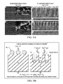
- FIG. 5A is a scanning electron microscope (SEM) photo of Si nanowire arrays on Si.
- FIG. 5B is an illustration of the metal-assisted chemical etching of localized regions in a silicon wafer.
- FIG. 6 is a flow diagram of the process used to mount a die according to an embodiment of this invention.
- the embodiments of the invention relate generally to the packaging of integrated circuits.
- the testing and operation of an integrated circuit (IC) package may subject the package to temperature extremes and other stresses. Such stresses may cause delamination and degrade the thermal performance of the package.
- the present invention provides a simple, cost-effective approach for die attached to lead frame surface.
- FIG. 1 illustrates a cross-sectional view of one embodiment of the present invention where a die 100 is secured to the die attach pad 101 with Silicon nanowires.
- the nanowires are between the 10 nm and 1 ⁇ m in diameter and 0.1-20 ⁇ m long and adhere the bottom of the die to the top surface of the die attach pad.
- the bottom surface of the die 100 includes a plurality of silicon nanowires.
- the bond between the die pad 101 and the back of the die 100 is obtained by applying pressure to the die/die attach pad combination. Pressure is typically in the range of 0.01-1 Megapascal (MPa).
- the silicon nanowire can be modified with Amine-based, sulfur-based and phosphorous-based silane coupling agents to substantially enhance the adhesion between silicon nanowire and lead frame surface.
- the die mount procedure mentioned above improves adhesion through increasing the bonding area and possibly forming mechanical interlocking using roughened lead frame, thus enabling enhanced package performance and reliability.
- Embodiments of the present invention will now be described with reference to FIGS. 2-6 .
- a particular embodiment of the regions pertaining to the die 100 , silicon nanowires, die attach pad 101 will be described.
- FIG. 2 is an exemplary sample of a semiconductor wafer 200 having top 201 and backside 202 surfaces.
- FIG. 3 illustrates application of metal nanoparticles to the backside of the wafer 200 .
- the particles are applied by printing the backside of the wafer with an ink containing metal nanoparticles.
- the metal nanoparticles can be Platinum (Pt), Gold (Au) or Silver (Ag).
- the ink is then dried to evaporate the volatile suspension vehicle.
- FIG. 4 shows the backside of the wafer after silicon nanowires, are formed utilizing Metal-assisted Chemical Etching to form the nanowires.
- FIG. 5B is a diagrammatic illustration of the Metal-Assisted Chemical Etching process.
- the etching is accomplished using the chemical reaction: Si+2H 2 O 2 +6HF ⁇ H 2 SiF 6 +2H 2 O+H 2
- a metal catalyst and a semiconductor interface form a cathode and anode, respectively.
- charge injection is sustained from a solution to the substrate and charge is balanced by the cathodic and anodic reactions.
- the presence of a local site for reaction the metal nanoparticle defines the selectivity of the etching mechanism.
- FIG. 5A shows a SEM photo of typical arrays of silicon nanowire arrays formed using the Metal-Assisted Chemical Etching process.
- Step 601 involves providing a semiconductor wafer containing integrated circuit die, having a top side and a bottom side.
- Step 602 involves depositing metal nanoparticles on the backside of the semiconductor wafer utilizing a printing process wherein the printing process prints ink containg metal nanoparticles on the wafer. The ink is then dried to allow the suspension vehicle in the ink to evaporate leaving the metal nanoparticles on the backside of the wafer.
- Step 603 involves etching cavities in backside of wafer using metal assisted chemical etching to form nanowires in the backside of wafer.
- the cavities formed in the backside of the wafer are typically less than 20 ⁇ m deep.
- Step 604 involves separating the integrated circuit die using a method selected from sawing, scribing and breaking or laser cutting.
- Step 605 involves providing a substrate for mounting the die.
- the substrate can be a lead frame, a laminate or a ceramic package.
- Step 606 involves adhering the backside of integrated circuit die to the top surface of the substrate with the nanowires therebetween.
- Adhering the backside of the integrated circuit die to the top surface of the substrate is accomplished by the physical phenomenon called the Van der Waals Force or chemical interaction if coupling agents are used.
- the Van der Waals Force is the sum of the attractive or repulsive forces between molecules (or between parts of the same molecule) other than those due to covalent bonds, the hydrogen bonds, or the electrostatic interaction of ions with one another or with neutral molecules or charge molecules. Since the backside of the die has a plurality of silicon nanowires, intimate contact is achieved with the substrate, which leads to the Van der Waals interaction.
Landscapes
- Engineering & Computer Science (AREA)
- Chemical & Material Sciences (AREA)
- Nanotechnology (AREA)
- Manufacturing & Machinery (AREA)
- Physics & Mathematics (AREA)
- Condensed Matter Physics & Semiconductors (AREA)
- General Physics & Mathematics (AREA)
- Crystallography & Structural Chemistry (AREA)
- Die Bonding (AREA)
Abstract
An apparatus for enhancing the thermal performance of semiconductor packages effectively. The concept of this invention is to provide silicon nanowires on the backside of an integrated circuit die to directly attach the die to the substrate, thereby improving the interface between die and substrate, and thus enhancing thermal performance and enhancing reliability by improving adhesion.
Description
This application is a Divisional of and claims priority to U.S. application Ser. No. 14/034,078, filed on Sep. 23, 2013. Said application is incorporated herein by reference.
The invention embodiments described herein relate generally to semiconductor device packaging and associated die attachment methods. In particular, the invention relates to cost effective packaging methods that provide high thermal performance at the interface of die to lead frame when implemented in molded packages. The principles herein are also applicable to other semiconductor packages and devices.
The embodiments of the invention relate generally to the packaging of integrated circuits (ICs); more particularly, a new die attach method suitable for use in packaging IC dice are described to eliminate die attach materials and reduce the cost, while providing good thermal performance and without the concern of resin bleed-out.
There are a number of conventional processes for packaging integrated circuit (IC) dice. By way of example, many IC packages utilize a metallic lead frame. The lead frame typically includes a plurality of leads or contacts, and optionally a die attach pad (paddle) upon which a die may be attached by means of a suitable adhesive material. The die is typically electrically connected to the lead frame leads by appropriate connectors such as bonding wires. In general, the die and portions of the lead frame are encapsulated with a molding material to protect the electrical connections and the delicate electrical components on the active side of the die.
The above-mentioned adhesive material can be in the format of paste (called die attach paste) or film (die attach film). Die attach paste, typically contains about 80 wt % silver filler and about 20 wt % polymer resin and additives. There are many limitations with die attach paste including resin bleed out (RBO), inconsistent die attach thickness, outgassing of organic components onto the bond pad on die surface causing non-stick on pad (NSOP) or causing the corrosion, and so on. Die attach film (DAF) has been developed to address some of the problems such as RBO and inconsistent die attach thickness. However, there are still some problems associated DAF such as limited thermal conductivity, sawing and die pickup issues. Moreover, the cost of DAF material is much higher than die attach paste.
On the other hand, much effort has been focused on gecko-inspired adhesives, which primarily rely on Van der Waals forces for adhesion by growing nanomaterials (such as carbon nanotubes) on the backside of the wafer or the chip. The growth temperature is about 750-850° C. However microelectronic chips cannot withstand so high temperature.
In view of the foregoing, there is continuing effort to produce cost effective packaging methods that provide high thermal performance at the interface of die to lead frame when implemented in molded packages.
The following presents a simplified summary in order to provide a basic understanding of one or more aspects of the invention. This summary is not an extensive overview of the invention, and is neither intended to identify key or critical elements of the invention, nor to delineate the scope thereof. Rather, the primary purpose of the summary is to present some concepts of the invention in a simplified form as a prelude to a more detailed description that is presented later.
In accordance with an embodiment of the present application, an apparatus is provided. The apparatus comprises: a semiconductor die, having a top side and a backside; a plurality of silicon nanowires formed on the backside of the semiconductor die; a substrate, having a top side with a die attach pad and a backside; wherein the backside of integrated circuit die is positioned on the die attach pad while maintaining the top surface of the die in a parallel with the top surface of the substrate; and wherein the semiconductor die is mechanically attached to the substrate by the silicon nanowires using pressure between 0.01 Megapascal MPa) and 1 MPa.
In accordance with another embodiment of the application, a method of attaching a semiconductor die to a substrate is provided. The method comprising the steps; providing a semiconductor wafer containing integrated circuits, wherein the wafer has a top side and a backside; printing an ink containing metal nanoparticles of the back side of the wafer; etching a plurality of cavities on the backside of the wafers using metal assisted chemical etching to form a plurality of silicon nanowires; separating the semiconductor wafer into individual integrated circuit die; providing a substrate, having a top side with a die attach pad, and a backside; positioning the backside of integrated circuit die on the die attach pad while maintaining the top surface of the die in a parallel with the top surface of the substrate; and attaching the integrated circuit die to the substrate by the silicon nanowires using pressure between 0.01 and 1 MPa.
In the drawings, like reference numerals are sometimes used to designate like structural elements. It should also be appreciated that the depictions in the figures are diagrammatic and not to scale.
The embodiments of the invention are described with reference to the attached figures. The figures are not drawn to scale and they are provided merely to illustrate the invention. Several aspects of the invention are described below with reference to example applications for illustration. It should be understood that numerous specific details, relationships, and methods are set forth to provide an understanding of the invention. One skilled in the relevant art, however, will readily recognize that the invention can be practiced without one or more of the specific details or with other methods. In other instances, well-known structures or operations are not shown in detail to avoid obscuring the invention. The embodiments of the invention are not limited by the illustrated ordering of acts or events, as some acts may occur in different orders and/or concurrently with other acts or events. Furthermore, not all illustrated acts or events are required to implement a methodology in accordance with the present invention.
The embodiments of the invention relate generally to the packaging of integrated circuits. As explained in the background section, the testing and operation of an integrated circuit (IC) package may subject the package to temperature extremes and other stresses. Such stresses may cause delamination and degrade the thermal performance of the package. The present invention provides a simple, cost-effective approach for die attached to lead frame surface.
Referring next to FIG. 1 , an improved packaging structure design in accordance with one aspect of the invention will be described. FIG. 1 illustrates a cross-sectional view of one embodiment of the present invention where a die 100 is secured to the die attach pad 101 with Silicon nanowires. The nanowires are between the 10 nm and 1 μm in diameter and 0.1-20 μm long and adhere the bottom of the die to the top surface of the die attach pad. The bottom surface of the die 100 includes a plurality of silicon nanowires.
The bond between the die pad 101 and the back of the die 100 is obtained by applying pressure to the die/die attach pad combination. Pressure is typically in the range of 0.01-1 Megapascal (MPa). In addition, the silicon nanowire can be modified with Amine-based, sulfur-based and phosphorous-based silane coupling agents to substantially enhance the adhesion between silicon nanowire and lead frame surface.
The die mount procedure mentioned above improves adhesion through increasing the bonding area and possibly forming mechanical interlocking using roughened lead frame, thus enabling enhanced package performance and reliability.
Embodiments of the present invention will now be described with reference to FIGS. 2-6 . A particular embodiment of the regions pertaining to the die 100, silicon nanowires, die attach pad 101 will be described.
Si+2H2O2+6HF→H2SiF6+2H2O+H2
As shown in the illustration in FIG. 5B , where a metal catalyst and a semiconductor interface form a cathode and anode, respectively. Through the metal catalyst, charge injection is sustained from a solution to the substrate and charge is balanced by the cathodic and anodic reactions. The presence of a local site for reaction the metal nanoparticle defines the selectivity of the etching mechanism.
Referring next to the flow chart 600 presented in FIG. 6 , one suitable approach for forming a package having good electrical and thermal performance and low delamination at the die-die attach pad interface will be described. Unless explicitly indicated otherwise, the operations described below may be performed concurrently or in any order. Operations may be added to or removed from flow chart 600.
Step 601 involves providing a semiconductor wafer containing integrated circuit die, having a top side and a bottom side.
Step 602 involves depositing metal nanoparticles on the backside of the semiconductor wafer utilizing a printing process wherein the printing process prints ink containg metal nanoparticles on the wafer. The ink is then dried to allow the suspension vehicle in the ink to evaporate leaving the metal nanoparticles on the backside of the wafer.
Step 603 involves etching cavities in backside of wafer using metal assisted chemical etching to form nanowires in the backside of wafer. The cavities formed in the backside of the wafer are typically less than 20 μm deep.
Step 604 involves separating the integrated circuit die using a method selected from sawing, scribing and breaking or laser cutting.
Step 605 involves providing a substrate for mounting the die. The substrate can be a lead frame, a laminate or a ceramic package.
Step 606 involves adhering the backside of integrated circuit die to the top surface of the substrate with the nanowires therebetween. Adhering the backside of the integrated circuit die to the top surface of the substrate is accomplished by the physical phenomenon called the Van der Waals Force or chemical interaction if coupling agents are used. The Van der Waals Force is the sum of the attractive or repulsive forces between molecules (or between parts of the same molecule) other than those due to covalent bonds, the hydrogen bonds, or the electrostatic interaction of ions with one another or with neutral molecules or charge molecules. Since the backside of the die has a plurality of silicon nanowires, intimate contact is achieved with the substrate, which leads to the Van der Waals interaction. The interaction with each silicon nanowire is small, however, since the total number of silicon nanowires is large, the total Van der Waals force is large enough to cause excellent self adhesion of the die to the substrate. Better adhesion can be further achieved with substrates through chemical modification of silicone nanowire surface with silane coupling agents or having a rough top surface contact area of a substrate such as roughened lead frame. Since there is no interface between die and silicon nanowires, the thermal performance will be effectively improved.
While various embodiments of the present invention have been described above, it should be understood that they have been presented by way of example only and not limitation. Numerous changes to the disclosed embodiments can be made in accordance with the disclosure herein without departing from the spirit or scope of the invention. Thus, the breadth and scope of the present invention should not be limited by any of the above described embodiments. Rather, the scope of the invention should be defined in accordance with the following claims and their equivalents.
Claims (18)
1. A semiconductor package comprising:
a semiconductor die, including an active side and an opposite back side, the opposite back side shaped as a plurality of nanowires, a plurality of cavities between the plurality of nanowires; and
a substrate having a first side, the opposite back side of the semiconductor die attached to the first side of the substrate.
2. The semiconductor package of claim 1 , wherein the plurality of nanowires are of silicon.
3. The semiconductor package of claim 1 , wherein the semiconductor die is pressure fit to the first side of the substrate via the plurality of nanowires.
4. The semiconductor package of claim 1 , wherein each of the plurality of nanowires is between 10 nanometers and 1 micrometer in diameter.
5. The semiconductor package of claim 1 , wherein each of the plurality of nanowires is less than 20 micrometer in length.
6. The semiconductor package of claim 1 , wherein the substrate is a laminate.
7. The semiconductor package of claim 1 , wherein the plurality of nanowires includes one of an amine based, a sulfur based, and a phosphorous based silane coupling agents.
8. The semiconductor package of claim 1 , wherein the substrate is a leadframe.
9. The semiconductor package of claim 8 , wherein the leadframe includes a die attach pad, the opposite back side of the semiconductor die being attached to the die attach pad.
10. The semiconductor package of claim 8 , wherein the leadframe includes a roughened surface that is in contact with the plurality of nanowires.
11. The semiconductor package of claim 1 , wherein the opposite back side of the semiconductor die is shaped as a plurality of nanowires by metal assisted chemical etching.
12. A semiconductor package comprising:
a semiconductor die, including an active side and an opposite back side, the opposite back side shaped as a plurality of nanowires, the opposite back side including a plurality of cavities in between the plurality of nanowires;
a substrate having a first side, the opposite back side of the semiconductor die attached to the first side of the substrate; and
mold compound in the plurality of cavities.
13. The semiconductor package of claim 12 , wherein each of the plurality of cavities is less than 20 μm deep.
14. The semiconductor package of claim 12 , wherein the plurality of nanowires includes one of an amine based, a sulfur based, and a phosphorous based silane coupling agents.
15. The semiconductor package of claim 12 , wherein the substrate is a leadframe.
16. The semiconductor package of claim 15 , wherein the leadframe includes a die attach pad, the opposite back side of the semiconductor die being attached to the die attach pad.
17. The semiconductor package of claim 12 , wherein the substrate is a laminate.
18. The semiconductor package of claim 12 , wherein the plurality of nanowires and the plurality of cavities together cover an entire area of the opposite back side.
Priority Applications (1)
| Application Number | Priority Date | Filing Date | Title |
|---|---|---|---|
| US14/541,208 US10312212B2 (en) | 2013-09-23 | 2014-11-14 | Self-adhesive die |
Applications Claiming Priority (2)
| Application Number | Priority Date | Filing Date | Title |
|---|---|---|---|
| US14/034,078 US8912637B1 (en) | 2013-09-23 | 2013-09-23 | Self-adhesive die |
| US14/541,208 US10312212B2 (en) | 2013-09-23 | 2014-11-14 | Self-adhesive die |
Related Parent Applications (1)
| Application Number | Title | Priority Date | Filing Date |
|---|---|---|---|
| US14/034,078 Division US8912637B1 (en) | 2013-09-23 | 2013-09-23 | Self-adhesive die |
Publications (2)
| Publication Number | Publication Date |
|---|---|
| US20150171046A1 US20150171046A1 (en) | 2015-06-18 |
| US10312212B2 true US10312212B2 (en) | 2019-06-04 |
Family
ID=52015245
Family Applications (2)
| Application Number | Title | Priority Date | Filing Date |
|---|---|---|---|
| US14/034,078 Active US8912637B1 (en) | 2013-09-23 | 2013-09-23 | Self-adhesive die |
| US14/541,208 Active 2033-12-11 US10312212B2 (en) | 2013-09-23 | 2014-11-14 | Self-adhesive die |
Family Applications Before (1)
| Application Number | Title | Priority Date | Filing Date |
|---|---|---|---|
| US14/034,078 Active US8912637B1 (en) | 2013-09-23 | 2013-09-23 | Self-adhesive die |
Country Status (2)
| Country | Link |
|---|---|
| US (2) | US8912637B1 (en) |
| CN (1) | CN104465533B (en) |
Families Citing this family (8)
| Publication number | Priority date | Publication date | Assignee | Title |
|---|---|---|---|---|
| US10134599B2 (en) * | 2016-02-24 | 2018-11-20 | The Board Of Trustees Of The University Of Illinois | Self-anchored catalyst metal-assisted chemical etching |
| US11031364B2 (en) | 2018-03-07 | 2021-06-08 | Texas Instruments Incorporated | Nanoparticle backside die adhesion layer |
| US11282807B2 (en) * | 2019-04-08 | 2022-03-22 | Texas Instruments Incorporated | Nanowires plated on nanoparticles |
| US11869864B2 (en) | 2019-04-08 | 2024-01-09 | Texas Instruments Incorporated | Nanowires plated on nanoparticles |
| US11239195B2 (en) * | 2019-04-08 | 2022-02-01 | Texas Instruments Incorporated | Nanowire interfaces |
| US11195811B2 (en) * | 2019-04-08 | 2021-12-07 | Texas Instruments Incorporated | Dielectric and metallic nanowire bond layers |
| WO2022162912A1 (en) * | 2021-01-29 | 2022-08-04 | サンケン電気株式会社 | Semiconductor device |
| US11610817B2 (en) | 2021-03-19 | 2023-03-21 | Infineon Technologies Austria Ag | Method of processing a semiconductor wafer, semiconductor wafer, and semiconductor die produced from a semiconductor wafer |
Citations (16)
| Publication number | Priority date | Publication date | Assignee | Title |
|---|---|---|---|---|
| US20040106203A1 (en) * | 2002-12-03 | 2004-06-03 | James Stasiak | Free-standing nanowire sensor and method for detecting an analyte in a fluid |
| US20040261987A1 (en) * | 2003-06-30 | 2004-12-30 | Yuegang Zhang | Thermal interface apparatus, systems, and methods |
| US20080150127A1 (en) * | 2006-12-21 | 2008-06-26 | Nachiket Raravikar | Microelectronic package, method of manufacturing same, and system containing same |
| US20090072408A1 (en) * | 2007-09-12 | 2009-03-19 | Smoltek Ab | Connecting and Bonding Adjacent Layers with Nanostructures |
| US7589403B2 (en) * | 2005-04-29 | 2009-09-15 | Infineon Technologies Ag | Lead structure for a semiconductor component and method for producing the same |
| US7727814B2 (en) | 2005-04-28 | 2010-06-01 | Intel Corporation | Microelectronic package interconnect and method of fabrication thereof |
| US7791194B2 (en) | 2008-04-10 | 2010-09-07 | Oracle America, Inc. | Composite interconnect |
| US7808089B2 (en) | 2007-12-18 | 2010-10-05 | National Semiconductor Corporation | Leadframe having die attach pad with delamination and crack-arresting features |
| US7838974B2 (en) | 2007-09-13 | 2010-11-23 | National Semiconductor Corporation | Intergrated circuit packaging with improved die bonding |
| US7859090B2 (en) | 2006-03-08 | 2010-12-28 | National Semiconductor Corporation | Die attach method and leadframe structure |
| US20110103020A1 (en) * | 2003-08-25 | 2011-05-05 | Carlos Dangelo | Carbon Nanotube-Based Structures and Methods for Removing Heat from Solid-State Devices |
| US20110309233A1 (en) * | 2010-06-22 | 2011-12-22 | President And Fellows Of Harvard College | Selected spectral absorption of nanowires |
| US20140126165A1 (en) * | 2012-11-06 | 2014-05-08 | Infineon Technologies Austria Ag | Packaged Nano-Structured Component and Method of Making a Packaged Nano-Structured Component |
| US8753924B2 (en) | 2012-03-08 | 2014-06-17 | Texas Instruments Incorporated | Grown carbon nanotube die attach structures, articles, devices, and processes for making them |
| US20150001697A1 (en) * | 2013-06-28 | 2015-01-01 | Stmicroelectronics Sdn Bhd | Selective treatment of leadframe with anti-wetting agent |
| US20150017802A1 (en) * | 2013-07-12 | 2015-01-15 | Bandgap Engineering, Inc. | Double-etch nanowire process |
Family Cites Families (1)
| Publication number | Priority date | Publication date | Assignee | Title |
|---|---|---|---|---|
| US7494910B2 (en) * | 2006-03-06 | 2009-02-24 | Micron Technology, Inc. | Methods of forming semiconductor package |
-
2013
- 2013-09-23 US US14/034,078 patent/US8912637B1/en active Active
-
2014
- 2014-09-18 CN CN201410478610.2A patent/CN104465533B/en active Active
- 2014-11-14 US US14/541,208 patent/US10312212B2/en active Active
Patent Citations (17)
| Publication number | Priority date | Publication date | Assignee | Title |
|---|---|---|---|---|
| US20040106203A1 (en) * | 2002-12-03 | 2004-06-03 | James Stasiak | Free-standing nanowire sensor and method for detecting an analyte in a fluid |
| US20040261987A1 (en) * | 2003-06-30 | 2004-12-30 | Yuegang Zhang | Thermal interface apparatus, systems, and methods |
| US20110103020A1 (en) * | 2003-08-25 | 2011-05-05 | Carlos Dangelo | Carbon Nanotube-Based Structures and Methods for Removing Heat from Solid-State Devices |
| US7727814B2 (en) | 2005-04-28 | 2010-06-01 | Intel Corporation | Microelectronic package interconnect and method of fabrication thereof |
| US7589403B2 (en) * | 2005-04-29 | 2009-09-15 | Infineon Technologies Ag | Lead structure for a semiconductor component and method for producing the same |
| US7859090B2 (en) | 2006-03-08 | 2010-12-28 | National Semiconductor Corporation | Die attach method and leadframe structure |
| US20080150127A1 (en) * | 2006-12-21 | 2008-06-26 | Nachiket Raravikar | Microelectronic package, method of manufacturing same, and system containing same |
| US8106517B2 (en) | 2007-09-12 | 2012-01-31 | Smoltek Ab | Connecting and bonding adjacent layers with nanostructures |
| US20090072408A1 (en) * | 2007-09-12 | 2009-03-19 | Smoltek Ab | Connecting and Bonding Adjacent Layers with Nanostructures |
| US7838974B2 (en) | 2007-09-13 | 2010-11-23 | National Semiconductor Corporation | Intergrated circuit packaging with improved die bonding |
| US7808089B2 (en) | 2007-12-18 | 2010-10-05 | National Semiconductor Corporation | Leadframe having die attach pad with delamination and crack-arresting features |
| US7791194B2 (en) | 2008-04-10 | 2010-09-07 | Oracle America, Inc. | Composite interconnect |
| US20110309233A1 (en) * | 2010-06-22 | 2011-12-22 | President And Fellows Of Harvard College | Selected spectral absorption of nanowires |
| US8753924B2 (en) | 2012-03-08 | 2014-06-17 | Texas Instruments Incorporated | Grown carbon nanotube die attach structures, articles, devices, and processes for making them |
| US20140126165A1 (en) * | 2012-11-06 | 2014-05-08 | Infineon Technologies Austria Ag | Packaged Nano-Structured Component and Method of Making a Packaged Nano-Structured Component |
| US20150001697A1 (en) * | 2013-06-28 | 2015-01-01 | Stmicroelectronics Sdn Bhd | Selective treatment of leadframe with anti-wetting agent |
| US20150017802A1 (en) * | 2013-07-12 | 2015-01-15 | Bandgap Engineering, Inc. | Double-etch nanowire process |
Non-Patent Citations (10)
| Title |
|---|
| Balasundaram, Karthik et al., Porosity control in metal-assisted chemical etching of degenerately doped silicon nanowires, IOP Publishing, 2012 Nanotechnology 23, pp. 7. |
| Dubrow, Zoe E., Characterization and Optimization of the Bonding Forces of a Novel Silicon Nanowire Gecko Biomimetic Adhesive, California State Fair, 2010 Project Summary. |
| Duran, S. et al., Silicon Nanovelcro to Attach Inorganci Microdevices to Biological Material, 14th International Conference on Miniaturized Systems for Chemistry and Life Sciences, Oct. 3-7, 2010, Groningen, The Netherlands, pp. 503-505. |
| Fischer, Kathleen E. et al, Biomimetic nanowire coatings for next generation adhesive drug delivery systems, Nano Lett. Feb. 2009; 9 (2): 716-720. |
| Ko, Hyunhyub et al., Thermoresponsive Chemical Connectors Based on Hybrid Nanowire Forests, Angew. Chem. Int. Ed. 2010, 49, 616-619. |
| Ko, Hyunhyub et al., Wet and Dry Adhesion Properties of Self-Selective Nanowire Connectors, Adv. Funct. Mater. 2009, 19, 3098-3102. |
| Mimicking Gecko Feet: Dry Adhesive Based on Carbon Nanotubes Gets Stronger, ScienceDaily, Georgia Institute of Technology, Oct. 10, 2008. |
| Qu, Liangti et al., Carbon Nanotube Arrays with Strong Shear Binding-On and Easy Normal Lifting-Off, Science, vol. 322, Oct. 10, 2013, pp. 238-242. |
| Shim, Hyun Woo et al., Strong friction of silicon carbide nanowire films, IOP Publishing, Nanotechnology 20 (2009), pp. 4. |
| Zhang, Ming Liang et al, Preparation of Large-Area Uniform Silicon Nanowires Arrays through Metal-Assisted Chemical Etching, J. Phys. Chem. C, vol. 112, No. 12, 2008, 4444-4450. |
Also Published As
| Publication number | Publication date |
|---|---|
| US20150171046A1 (en) | 2015-06-18 |
| CN104465533A (en) | 2015-03-25 |
| CN104465533B (en) | 2019-08-16 |
| US8912637B1 (en) | 2014-12-16 |
Similar Documents
| Publication | Publication Date | Title |
|---|---|---|
| US10312212B2 (en) | Self-adhesive die | |
| CN101572239B (en) | Semiconductor module | |
| US9780017B2 (en) | Packaged device with additive substrate surface modification | |
| US9478484B2 (en) | Semiconductor packages and methods of formation thereof | |
| US8872315B2 (en) | Electronic device and method of fabricating an electronic device | |
| JP2019515509A (en) | Floating die package | |
| CN107863327A (en) | Packaging body with the roughening encapsulating surface for promoting adhesion | |
| US20150069600A1 (en) | Embedded Silver Nanomaterials into Die Backside to Enhance Package Performance and Reliability | |
| US9941210B1 (en) | Semiconductor devices with protruding conductive vias and methods of making such devices | |
| CN103367321A (en) | Chip arrangement and a method for forming a chip arrangement | |
| JP7070971B2 (en) | Enhanced adhesion by a layer of nanoparticles with randomly constructed voids | |
| KR20180016307A (en) | Die attach methods and semiconductor devices manufactured based on such methods | |
| US7821117B2 (en) | Semiconductor package with mechanical stress isolation of semiconductor die subassembly | |
| US11676930B2 (en) | Nanoparticle backside die adhesion layer | |
| US10784188B2 (en) | Methods and apparatus for a semiconductor device having bi-material die attach layer | |
| CN103515311B (en) | The method of chip package and manufacture chip package | |
| TWI637470B (en) | Semiconductor package and manufacturing method thereof | |
| US8288207B2 (en) | Method of manufacturing semiconductor devices | |
| CN103325752A (en) | Circuit package, electronic circuit package, and method for encapsulating an electronic circuit | |
| CN107275230A (en) | Semiconductor package assembly and a manufacturing method thereof | |
| CN103803488A (en) | Packaged nano-structured component and method of making a packaged nano-structured component | |
| CN117012742A (en) | Methods, corresponding devices and systems for manufacturing semiconductor devices | |
| JP2018037639A (en) | Semiconductor package and method for manufacturing semiconductor package | |
| CN101494210A (en) | Conductor frame and encapsulation structure | |
| CN107170715A (en) | Semiconductor package structure and manufacturing method thereof |
Legal Events
| Date | Code | Title | Description |
|---|---|---|---|
| STPP | Information on status: patent application and granting procedure in general |
Free format text: NOTICE OF ALLOWANCE MAILED -- APPLICATION RECEIVED IN OFFICE OF PUBLICATIONS |
|
| STCF | Information on status: patent grant |
Free format text: PATENTED CASE |
|
| MAFP | Maintenance fee payment |
Free format text: PAYMENT OF MAINTENANCE FEE, 4TH YEAR, LARGE ENTITY (ORIGINAL EVENT CODE: M1551); ENTITY STATUS OF PATENT OWNER: LARGE ENTITY Year of fee payment: 4 |