US10305446B2 - Piezoelectric oscillator and method of making the same - Google Patents
Piezoelectric oscillator and method of making the same Download PDFInfo
- Publication number
- US10305446B2 US10305446B2 US15/179,248 US201615179248A US10305446B2 US 10305446 B2 US10305446 B2 US 10305446B2 US 201615179248 A US201615179248 A US 201615179248A US 10305446 B2 US10305446 B2 US 10305446B2
- Authority
- US
- United States
- Prior art keywords
- oscillating
- electrodes
- piezoelectric oscillator
- oscillation substrate
- oscillation
- Prior art date
- Legal status (The legal status is an assumption and is not a legal conclusion. Google has not performed a legal analysis and makes no representation as to the accuracy of the status listed.)
- Active, expires
Links
- 238000004519 manufacturing process Methods 0.000 title abstract description 8
- 230000010355 oscillation Effects 0.000 claims abstract description 77
- 239000000758 substrate Substances 0.000 claims abstract description 72
- 239000013078 crystal Substances 0.000 claims description 59
- 235000012431 wafers Nutrition 0.000 description 23
- 238000000034 method Methods 0.000 description 9
- 239000000306 component Substances 0.000 description 7
- PXHVJJICTQNCMI-UHFFFAOYSA-N Nickel Chemical compound [Ni] PXHVJJICTQNCMI-UHFFFAOYSA-N 0.000 description 6
- 239000010931 gold Substances 0.000 description 6
- 238000005530 etching Methods 0.000 description 5
- -1 regions Substances 0.000 description 5
- 230000008859 change Effects 0.000 description 4
- 230000000694 effects Effects 0.000 description 4
- 229910000679 solder Inorganic materials 0.000 description 4
- 239000000853 adhesive Substances 0.000 description 3
- 230000001070 adhesive effect Effects 0.000 description 3
- PCHJSUWPFVWCPO-UHFFFAOYSA-N gold Chemical compound [Au] PCHJSUWPFVWCPO-UHFFFAOYSA-N 0.000 description 3
- 229910052737 gold Inorganic materials 0.000 description 3
- 239000000463 material Substances 0.000 description 3
- 239000002184 metal Substances 0.000 description 3
- 229910052751 metal Inorganic materials 0.000 description 3
- 239000010453 quartz Substances 0.000 description 3
- 239000011347 resin Substances 0.000 description 3
- 229920005989 resin Polymers 0.000 description 3
- VYPSYNLAJGMNEJ-UHFFFAOYSA-N silicon dioxide Inorganic materials O=[Si]=O VYPSYNLAJGMNEJ-UHFFFAOYSA-N 0.000 description 3
- 230000008878 coupling Effects 0.000 description 2
- 238000010168 coupling process Methods 0.000 description 2
- 238000005859 coupling reaction Methods 0.000 description 2
- 229910000833 kovar Inorganic materials 0.000 description 2
- 229910052759 nickel Inorganic materials 0.000 description 2
- 239000011368 organic material Substances 0.000 description 2
- 238000004088 simulation Methods 0.000 description 2
- 238000003466 welding Methods 0.000 description 2
- 230000008901 benefit Effects 0.000 description 1
- 238000003486 chemical etching Methods 0.000 description 1
- 238000004891 communication Methods 0.000 description 1
- 238000010276 construction Methods 0.000 description 1
- 239000008358 core component Substances 0.000 description 1
- 238000005520 cutting process Methods 0.000 description 1
- 238000013016 damping Methods 0.000 description 1
- 238000006073 displacement reaction Methods 0.000 description 1
- 238000010894 electron beam technology Methods 0.000 description 1
- 230000010358 mechanical oscillation Effects 0.000 description 1
- 238000002844 melting Methods 0.000 description 1
- 230000008018 melting Effects 0.000 description 1
- 229910052753 mercury Inorganic materials 0.000 description 1
- 238000012986 modification Methods 0.000 description 1
- 230000004048 modification Effects 0.000 description 1
- 230000000149 penetrating effect Effects 0.000 description 1
- 230000000704 physical effect Effects 0.000 description 1
- 238000007517 polishing process Methods 0.000 description 1
- 238000002360 preparation method Methods 0.000 description 1
- 238000007639 printing Methods 0.000 description 1
- 230000008569 process Effects 0.000 description 1
Images


Classifications
-
- H—ELECTRICITY
- H03—ELECTRONIC CIRCUITRY
- H03H—IMPEDANCE NETWORKS, e.g. RESONANT CIRCUITS; RESONATORS
- H03H9/00—Networks comprising electromechanical or electro-acoustic elements; Electromechanical resonators
- H03H9/02—Details
- H03H9/05—Holders or supports
- H03H9/0538—Constructional combinations of supports or holders with electromechanical or other electronic elements
- H03H9/0547—Constructional combinations of supports or holders with electromechanical or other electronic elements consisting of a vertical arrangement
-
- H—ELECTRICITY
- H03—ELECTRONIC CIRCUITRY
- H03H—IMPEDANCE NETWORKS, e.g. RESONANT CIRCUITS; RESONATORS
- H03H3/00—Apparatus or processes specially adapted for the manufacture of impedance networks, resonating circuits, resonators
- H03H3/007—Apparatus or processes specially adapted for the manufacture of impedance networks, resonating circuits, resonators for the manufacture of electromechanical resonators or networks
- H03H3/02—Apparatus or processes specially adapted for the manufacture of impedance networks, resonating circuits, resonators for the manufacture of electromechanical resonators or networks for the manufacture of piezoelectric or electrostrictive resonators or networks
-
- H—ELECTRICITY
- H03—ELECTRONIC CIRCUITRY
- H03H—IMPEDANCE NETWORKS, e.g. RESONANT CIRCUITS; RESONATORS
- H03H9/00—Networks comprising electromechanical or electro-acoustic elements; Electromechanical resonators
- H03H9/02—Details
- H03H9/02007—Details of bulk acoustic wave devices
- H03H9/02015—Characteristics of piezoelectric layers, e.g. cutting angles
- H03H9/02023—Characteristics of piezoelectric layers, e.g. cutting angles consisting of quartz
-
- H—ELECTRICITY
- H03—ELECTRONIC CIRCUITRY
- H03H—IMPEDANCE NETWORKS, e.g. RESONANT CIRCUITS; RESONATORS
- H03H9/00—Networks comprising electromechanical or electro-acoustic elements; Electromechanical resonators
- H03H9/02—Details
- H03H9/02007—Details of bulk acoustic wave devices
- H03H9/02157—Dimensional parameters, e.g. ratio between two dimension parameters, length, width or thickness
-
- H—ELECTRICITY
- H03—ELECTRONIC CIRCUITRY
- H03H—IMPEDANCE NETWORKS, e.g. RESONANT CIRCUITS; RESONATORS
- H03H9/00—Networks comprising electromechanical or electro-acoustic elements; Electromechanical resonators
- H03H9/02—Details
- H03H9/05—Holders or supports
- H03H9/10—Mounting in enclosures
-
- H—ELECTRICITY
- H03—ELECTRONIC CIRCUITRY
- H03H—IMPEDANCE NETWORKS, e.g. RESONANT CIRCUITS; RESONATORS
- H03H9/00—Networks comprising electromechanical or electro-acoustic elements; Electromechanical resonators
- H03H9/15—Constructional features of resonators consisting of piezoelectric or electrostrictive material
- H03H9/17—Constructional features of resonators consisting of piezoelectric or electrostrictive material having a single resonator
- H03H9/19—Constructional features of resonators consisting of piezoelectric or electrostrictive material having a single resonator consisting of quartz
-
- H—ELECTRICITY
- H03—ELECTRONIC CIRCUITRY
- H03H—IMPEDANCE NETWORKS, e.g. RESONANT CIRCUITS; RESONATORS
- H03H3/00—Apparatus or processes specially adapted for the manufacture of impedance networks, resonating circuits, resonators
- H03H3/007—Apparatus or processes specially adapted for the manufacture of impedance networks, resonating circuits, resonators for the manufacture of electromechanical resonators or networks
- H03H3/02—Apparatus or processes specially adapted for the manufacture of impedance networks, resonating circuits, resonators for the manufacture of electromechanical resonators or networks for the manufacture of piezoelectric or electrostrictive resonators or networks
- H03H2003/022—Apparatus or processes specially adapted for the manufacture of impedance networks, resonating circuits, resonators for the manufacture of electromechanical resonators or networks for the manufacture of piezoelectric or electrostrictive resonators or networks the resonators or networks being of the cantilever type
Definitions
- the following description relates to a piezoelectric oscillator and method of making the same.
- a piezoelectric oscillator is a device generating oscillations having a certain frequency through a piezoelectric material oscillating due to a piezoelectric phenomenon occurring when a voltage is applied to the piezoelectric oscillator. Since the piezoelectric oscillator has a stable oscillation frequency, such a device has been used in several core components providing a reference signal value as well as in an oscillation circuit of a computer or a communications device.
- a piezoelectric oscillator includes a crystal, an oscillation substrate using the crystal as a base material and an electrode disposed on the oscillation substrate, wherein the oscillation substrate may have various shapes depending on required physical properties.
- a piezoelectric oscillator When a piezoelectric oscillator is formed so that a thickness of the oscillation substrate is gradually reduced from a central portion thereof toward end portions thereof and is in a thickness shear oscillation mode, a damping amount of oscillation displacement in the end portion is increased.
- an effect in which oscillation energy is trapped in the central portion of the piezoelectric oscillator may be improved, and frequency characteristics such as a CI value and a Q value, may also be improved.
- An example of a shape of the piezoelectric oscillator that may accomplish an oscillation energy trapping effect may include a convex shape in which a convex curved surface is formed as a main surface, a bevel shape in which a space between a flat and thick central portion and an edge of an end portion is formed as an inclined surface, and a mesa, or stepped, shape in which a central portion is flat and a surrounding portion of the central portion is thin.
- a piezoelectric oscillator includes an oscillation substrate comprising an oscillating part and a surrounding part, wherein the surrounding part is thinner than the oscillating part, and oscillating electrodes disposed on an upper surface and a lower surface of the oscillating part.
- the oscillation substrate may be an AT-cut crystal.
- the x-axis direction of the crystal may be a length direction of the oscillation substrate.
- the oscillation substrate may include a first step corresponding to a step between an upper surface of the oscillating part and a first surface of the surrounding part, and a second step corresponding to a step between a lower surface of the oscillating part and a second surface of the surrounding part.
- the first step and the second step may have a same height.
- Terminal electrodes may be disposed on a first surface and a second surface of the surrounding part and connecting electrodes connecting the terminal electrodes to the oscillating electrodes.
- a piezoelectric oscillator in another general aspect, includes a lower case, an upper case disposed on the lower case, wherein disposed within the upper case and the lower case is an oscillation substrate having an oscillating part, a surrounding part.
- the surrounding part is thinner than the oscillating part, and oscillating electrodes are disposed on an upper surface and a lower surface of the oscillating part.
- Connection electrodes are disposed on an upper surface of the lower case and electrically connected to the oscillating electrodes, and external electrodes are disposed on a lower surface of the lower case and electrically connected to the connection electrodes.
- An electrode part may include terminal electrodes disposed on a first surface of the surrounding part and connected to the oscillating electrodes.
- Connection parts may be disposed between the terminal electrodes and the connection electrodes, and electrically connect the terminal electrodes to the connection electrodes.
- the oscillation substrate may be an AT-cut crystal.
- the x-axis direction of the crystal may be a length direction of the oscillation substrate.
- the oscillation substrate may include a first step corresponding to a step between an upper surface of the oscillating part and a first surface of the surrounding part and a second step corresponding to a step between a lower surface of the oscillating part and a second surface of the surrounding part.
- the first step and the second step may have a same height.
- Connecting electrodes may connect the terminal electrodes to the oscillating electrodes.
- L 1 represents an entire length of the oscillation substrate
- L 2 represents a length of the oscillating part
- T 1 represents a thickness of the oscillating part
- T 2 represents a step height between the oscillating part and the surrounding part.
- An electrode part may include terminal electrodes disposed on a first surface of the surrounding part and may be connected to the oscillating electrodes. Connection parts may be disposed between the terminal electrodes and the connection electrodes, and may electrically connect the terminal electrodes to the connection electrodes.
- the oscillation substrate may include a first step corresponding to a step between an upper surface of the oscillating part and a first surface of the surrounding part, and a second step corresponding to a step between a lower surface of the oscillating part and a second surface of the surrounding part.
- the method may further include forming an external electrode on an lower exterior surface of a lower case, forming a via, in the lower case, electrically connected to the external electrode, forming a connection electrode, on the lower case, electrically connected to the via and external electrode, and disposing the oscillation substrate in the lower case, wherein the electrode part on the oscillation substrate is electrically connected to the connection electrode.
- FIG. 1 is a perspective view of a piezoelectric oscillator according to an embodiment
- FIG. 2 is a cross-sectional view of the piezoelectric oscillator taken along line A-A′ of FIG. 1 ;
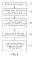
- FIG. 3 is a flow chart illustrating a method of manufacturing a piezoelectric oscillator according to an embodiment
- FIG. 4 is an exploded perspective view of a piezoelectric oscillator according to an another embodiment
- FIG. 5 is a cross-sectional view of the piezoelectric oscillator taken along line B-B′ of FIG. 4 ;
- FIGS. 6 through 8 are graphs illustrating simulation results representing a change in crystal impedance (CI) according to a change in an H value with respect to a specific S of a piezoelectric oscillator according to an Experimental Example;
- FIG. 9 is a graph illustrating a relationship of an H value representing a stable crystal impedance (CI) value according to an S value.
- first, second, third, etc. may be used herein to describe various members, components, regions, layers and/or sections, these members, components, regions, layers and/or sections should not be limited by these terms. These terms are only used to distinguish one member, component, region, layer or section from another region, layer or section. Thus, a first member, component, region, layer or section discussed below could be termed a second member, component, region, layer or section without departing from the teachings of the embodiments.
- a statement that a first layer is “on” a second layer or a substrate is to be interpreted as covering both a case where the first layer directly contacts the second layer or the substrate, and a case where one or more other layers are disposed between the first layer and the second layer or the substrate.
- Words describing relative spatial relationships such as “below”, “beneath”, “under”, “lower”, “bottom”, “above”, “over”, “upper”, “top”, “left”, and “right”, may be used to conveniently describe spatial relationships of one device or elements with other devices or elements. Such words are to be interpreted as encompassing a device oriented as illustrated in the drawings, and in other orientations in use or operation. For example, an example in which a device includes a second layer disposed above a first layer based on the orientation of the device illustrated in the drawings also encompasses the device when the device is flipped upside down in use or operation.
- FIG. 1 is a perspective view of a piezoelectric oscillator 100 according to an embodiment in the present disclosure.
- FIG. 2 is a cross-sectional view of the piezoelectric oscillator 100 taken along line A-A′ of FIG. 1 .
- the piezoelectric oscillator 100 includes an oscillation substrate 110 and an electrode part 120 disposed on the oscillation substrate 110 .
- An x-axis direction, a y-axis direction, and a z-axis direction illustrated in FIGS. 1 and 2 refer to a length direction, a thickness direction, and a width direction of the oscillation substrate, respectively.
- the oscillation substrate 110 is formed of crystal having an AT-cut, and a length direction (x-axis direction) of the oscillation substrate, which is a long side direction, refers to an x-axis direction of the crystal.
- the crystal serves as the mechanical oscillation generator.
- the crystal may be quartz.
- the oscillation substrate 110 includes an oscillating part 112 having a relatively increased thickness and a surrounding part 111 having a thickness less than that of the oscillating part, wherein the oscillating part 112 includes protruding parts 112 a and 112 b corresponding to regions extending from a first surface and a second surface, respectively, of the surrounding part 111 in a thickness, or y-axis, direction.
- the protruding parts includes a first protruding part 112 a extending further in the y-axis direction, or thickness direction, than the first surface of the surrounding part 111 and a second protruding part 112 b extending further in the opposite direction, along the y-axis or thickness direction, than the second surface of the surrounding part 111 .
- the electrode part 120 includes oscillating electrodes 121 a and 121 b disposed on the first surface and the second surface of the oscillating part 112 , terminal electrodes 123 a and 123 b disposed on the first surface or the second surface, or both surfaces, of the surrounding part 111 , and a connecting electrode 122 a connecting the oscillating electrodes 121 a and 121 b and the terminal electrodes 123 a and 123 b to each other.
- a first oscillating electrode 121 a is disposed on an upper surface of the oscillating part 112 and connected to a first terminal electrode 123 a through a first connecting electrode 122 a
- a second oscillating electrode 121 b is disposed on a lower surface of the oscillating part 112 opposite the upper surface and connected to a second terminal electrode 123 b through a second connecting electrode.
- the first terminal electrode 123 a extends along the first surface to a side surface of the surrounding part 111 , wraps around the side surface, and extends along the second surface of the surrounding part 111 .
- the second terminal electrode 123 b extends from the second surface to the side surface of the surrounding part 111 , wraps around the side surface, and extends along the first surface of the surrounding part 111 .
- the first terminal electrode 123 a and the second terminal electrode 123 b are not limited thereto and may be varied.
- the upper surface and the lower surface STa and STb of the first and second protruding parts 112 a and 112 b may have a substantially quadrangular shape, although they do not have a completely quadrangular shape due to etching of corner portions thereof.
- L 1 refers to an entire length of the oscillation substrate 110 along the x-axis direction of the crystal
- L 2 refers to a length of the oscillating part 112 measured in the x-axis direction of the crystal
- T 1 refers to an overall thickness of the oscillating part 112
- T 2 refers to a step height between the protruding parts 112 a and 112 b and the surrounding part 111 .
- a step between the oscillating part 112 and the surrounding part 111 includes a first step at one side of the oscillation substrate 110 in the thickness direction and a second step at the other side of the oscillation substrate 110 in the thickness direction.
- a height of the first step refers to a height difference between an upper surface STa of the first protruding part 112 a and an upper surface of the surrounding part 111
- a height of the second step refers to a height difference between a lower surface STb of the second protruding part 112 b and a lower surface of the surrounding part 111 .
- H 400.59 ⁇ S+ 1.75 ⁇ 1.5 [Equation 1]
- H is defined as a percentage (%) of the step height to the thickness of the oscillating part.
- ⁇ 1.5 is considered to be ⁇ 1.5% when determining H in Equation 1.
- a correlation between the entire length L 1 of the oscillation substrate 110 , the length L 2 of the oscillating part 112 , the thickness T 1 of the oscillating part 112 , and the step height T 2 between the oscillating part 112 and the surrounding part 111 may be derived in consideration of the length L 2 of the oscillating part 112 and the step height T 2 between the oscillating part 112 and the surrounding part 111 as well as the thickness T 1 of the oscillating part 112 and the entire length L 1 of the oscillation substrate 110 , thereby providing the piezoelectric oscillator 100 having high oscillation performance.
- a piezoelectric oscillator having low and stable crystal impedance (CI) may be achieved.
- the first step and the second step may be formed of the same height.
- the height T 2 of the step may be a half of a thickness difference between the overall thickness oscillating part 112 (e.g. T 1 ) and the surrounding part 111 .
- the first step and the second step have the same dimensions in the oscillation substrate, an energy trapping effect for frequency generation through a piezoelectric effect may be improved, thereby reducing energy loss.
- side surfaces of the protruding parts 112 a and 112 b are perpendicular to the upper surface of the oscillating part 112 and the upper surface of the surrounding part 111 in FIG. 2
- the side surfaces of the protruding parts are not limited thereto and may be varied. That is, the side surfaces of the protruding parts may be inclined with respect to the upper surface of the oscillating part and the upper surface of the surrounding part.
- the side surfaces of the protruding parts may have a single crystal face or two or more crystal faces.
- the piezoelectric oscillator is not limited to being manufactured by a method described below, and may be manufactured by various methods.
- FIG. 3 is a flow chart illustrating a method of manufacturing a piezoelectric oscillator according to an embodiment.
- the method of manufacturing a piezoelectric oscillator includes preparing a crystal wafer (S 1 ), forming resist patterns on upper and lower surfaces of the crystal wafer (S 2 ), forming protruding parts on the crystal wafer (S 3 ), removing the resist patterns (S 4 ), and forming an electrode part on a oscillation substrate formed by etching the crystal wafer (S 5 ).
- a single crystal wafer corresponding to a size of one oscillation substrate may be used, or a plurality of crystal wafers corresponding to the size of one oscillation substrate may be formed on a single crystal wafer assembly.
- the crystal wafer is formed by processing rough quartz in a quadrangular or circular shape and then cutting the rough quartz at a predetermined thickness.
- the crystal wafer is not limited a quadrangular or circular shape, and may have various shapes, such as a polygonal shape.
- a surface polishing process may be additionally performed on the crystal wafer in order to decrease a thickness of the crystal wafer.
- resist patterns are formed on one surface and another surface of the crystal wafer (S 2 ).
- the resist patterns are disposed on the crystal wafer according to the desired shapes and sizes of the protruding parts.
- the crystal wafer on which the resist patterns are disposed is etched to form the protruding parts on the one surface and the other surface of the crystal wafer (S 3 ).
- the crystal wafer may be etched by a chemical etching method by immersing the crystal wafer on which the resist patterns are formed in an etchant.
- an electrode part 120 is formed on the oscillation substrate 110 formed by etching (S 5 ).
- the electrode part 120 includes the oscillating electrodes 121 a and 121 b , the terminal electrodes 123 a and 123 b , and the connecting electrodes 122 a .
- the electrode part 120 may be formed by printing conductive pastes on the oscillation substrate on which the protruding parts 112 a and 112 b are formed.
- the electrode part 120 may have the oscillating electrodes 121 a and 121 b formed on an upper surface and a lower surface of the protruding parts 112 a and 112 b which make up the oscillation substrate 112 .
- FIG. 4 is an exploded perspective view of a piezoelectric oscillator 200 according to another embodiment
- FIG. 5 is a cross-sectional view of the piezoelectric oscillator 200 taken along line B-B′ of FIG. 4 .
- the piezoelectric oscillator 200 includes an oscillation substrate 110 having an electrode part 120 , as described above in the previous embodiment, and further includes a lower case 210 , an upper case 220 , connection electrodes 211 a and 211 b and external electrodes 212 a and 212 b.
- the lower case 210 and the upper case 220 are coupled to each other to form one case having an internal space, and the oscillation substrate 110 is disposed with in the internal space formed by coupling the upper case to the lower case.
- the oscillation substrate 110 is disposed in the lower case 210 and the upper case 220 in order to be protected from the external environment.
- connection electrodes include first and second connection electrodes 211 a and 211 b disposed spaced apart from each other.
- the external electrodes include first and second external electrodes 212 a and 212 b spaced apart from each other.
- the first and second connection electrodes 211 a and 211 b are disposed on an upper surface of an inner portion of the lower case 210 and connected to the first and second terminal electrodes 123 a and 123 b of the electrode part 120 , respectively.
- the first and second external electrodes 212 a and 212 b are disposed on a lower surface of an outer portion of the lower case 210 and connected to the first and second connection electrodes 211 a and 211 b , respectively.
- the first and second external electrodes 212 a and 212 b and the first and second connection electrodes 211 a and 211 b are connected to each other by via electrodes 213 a and 213 b penetrating through the lower case 210 , but are not limited thereto, and may be varied.
- the first and second external electrodes 212 a and 212 b may serve as input and output electrodes of the piezoelectric oscillator 200 . As described above, when a voltage is applied to the first and second external electrodes 212 a and 212 b , a voltage may be applied to the first and second oscillating electrodes 121 a and 121 b of the oscillation substrate 110 , and thus the oscillation substrate 110 may vibrate.
- connection parts 230 may include solder or conductive adhesive disposed between the first and second terminal electrodes 123 a and 123 b and the first and second connection electrodes 211 a and 211 b .
- the connection parts 230 electrically connect the first and second terminal electrodes 123 a and 123 b to the first and second connection electrodes 211 a and 211 b.
- the connection part 230 may further include a metal solder.
- the first and second connection electrodes 211 a and 211 b and the first and second terminal electrodes 123 a and 123 b may be connected to each other by disposing the metal solder on the first and second connection electrodes 211 a and 211 b , disposing the first and second terminal electrodes 123 a and 123 b on the metal solders, and then performing a reflow process.
- connection parts 230 may be formed by disposing nickel (Ni), gold (Au), or Kovar between the first and second connection electrodes 211 a and 211 b and the first and second terminal electrodes 123 a and 123 b and performing arc welding or electron beam welding on a coupling part such as the nickel (Ni), the gold (Au), or the Kovar, or melting gold (Au)-mercury (Hg) at a high temperature.
- a coupling part such as the nickel (Ni), the gold (Au), or the Kovar, or melting gold (Au)-mercury (Hg) at a high temperature.
- the method of forming the connection parts 230 is not limited thereto, and may be varied.
- connection parts 230 may include conductive adhesives that may contain a resin or another organic material, or both.
- a conductive adhesive containing a resin or an organic material air pressure between the oscillation substrate 110 and the connection electrodes 211 a and 211 b may be increased, and generation of cracks may be prevented.
- the upper case 220 and the lower case 210 may contain the same material, for example, an insulating resin, or the like, but are not limited thereto, and may be varied.
- H represents low and stable crystal impedance (CI) in the vicinity of 4.08.
- H represents low and stable crystal impedance (CI) in the vicinity of 4.79.
- H represents low and stable crystal impedance (CI) in the vicinity of 11.06.
- FIG. 9 is a graph, derived from the results of FIGS. 6 through 8 , illustrating a relationship of an H value representing stable crystal impedance (CI) value according to on an S value.
- CI stable crystal impedance
- the piezoelectric oscillator having low and stable crystal impedance may be achieved.
Landscapes
- Physics & Mathematics (AREA)
- Acoustics & Sound (AREA)
- Engineering & Computer Science (AREA)
- Manufacturing & Machinery (AREA)
- Piezo-Electric Or Mechanical Vibrators, Or Delay Or Filter Circuits (AREA)
- Oscillators With Electromechanical Resonators (AREA)
Abstract
Description
H=400.59×S+1.75±1.5 [Equation 1]
Claims (13)
[100×(T2/T1)]=400.59×[T2/(L1−L2)]+1.75±1.5,
[100×(T2/T1)]=400.59×[T2/(L1−L2)]+1.75±1.5,
Applications Claiming Priority (2)
| Application Number | Priority Date | Filing Date | Title |
|---|---|---|---|
| KR1020150126292A KR102163053B1 (en) | 2015-09-07 | 2015-09-07 | Piezoelectric vibration piece, and piezoelectric device |
| KR10-2015-0126292 | 2015-09-07 |
Publications (2)
| Publication Number | Publication Date |
|---|---|
| US20170070208A1 US20170070208A1 (en) | 2017-03-09 |
| US10305446B2 true US10305446B2 (en) | 2019-05-28 |
Family
ID=58190707
Family Applications (1)
| Application Number | Title | Priority Date | Filing Date |
|---|---|---|---|
| US15/179,248 Active 2037-05-06 US10305446B2 (en) | 2015-09-07 | 2016-06-10 | Piezoelectric oscillator and method of making the same |
Country Status (3)
| Country | Link |
|---|---|
| US (1) | US10305446B2 (en) |
| KR (1) | KR102163053B1 (en) |
| CN (1) | CN106505964B (en) |
Families Citing this family (2)
| Publication number | Priority date | Publication date | Assignee | Title |
|---|---|---|---|---|
| US9762206B2 (en) * | 2014-02-07 | 2017-09-12 | Samsung Electro-Mechanics Co., Ltd. | AT-cut quartz crystal vibrator with a long side along the X-axis direction |
| KR102117476B1 (en) * | 2015-07-01 | 2020-06-01 | 삼성전기주식회사 | Crystal oscillator and crystal oscillator package including the same |
Citations (6)
| Publication number | Priority date | Publication date | Assignee | Title |
|---|---|---|---|---|
| US20070096596A1 (en) * | 2005-10-31 | 2007-05-03 | Epson Toyocom Corporation | Mesa-shaped piezoelectric resonator element |
| JP2008263387A (en) | 2007-04-11 | 2008-10-30 | Epson Toyocom Corp | Mesa-type piezoelectric vibrating piece |
| JP2010109526A (en) | 2008-10-29 | 2010-05-13 | Epson Toyocom Corp | Crystal vibration piece, and method of manufacturing the same |
| US20120056514A1 (en) * | 2010-09-02 | 2012-03-08 | Nihon Dempa Kogyo Co., Ltd. | Mesa-Type At-Cut Quartz-Crystal Vibrating Piece and Quartz-Crystal Device |
| US20120126668A1 (en) * | 2010-11-19 | 2012-05-24 | Seiko Epson Corporation | Piezoelectric resonator element and piezoelectric resonator |
| JP2014116977A (en) | 2014-02-05 | 2014-06-26 | Seiko Epson Corp | Vibration piece and vibrator |
Family Cites Families (4)
| Publication number | Priority date | Publication date | Assignee | Title |
|---|---|---|---|---|
| JP4341583B2 (en) * | 2005-06-02 | 2009-10-07 | エプソントヨコム株式会社 | Mesa crystal unit |
| JP5015229B2 (en) * | 2009-12-24 | 2012-08-29 | 日本電波工業株式会社 | Crystal oscillator |
| JP5708089B2 (en) * | 2011-03-18 | 2015-04-30 | セイコーエプソン株式会社 | Piezoelectric vibration element, piezoelectric vibrator, piezoelectric oscillator, and electronic device |
| DE102012202575A1 (en) * | 2012-02-20 | 2013-08-22 | Siemens Aktiengesellschaft | Gas power plant |
-
2015
- 2015-09-07 KR KR1020150126292A patent/KR102163053B1/en active Active
-
2016
- 2016-06-10 US US15/179,248 patent/US10305446B2/en active Active
- 2016-07-05 CN CN201610523219.9A patent/CN106505964B/en not_active Expired - Fee Related
Patent Citations (6)
| Publication number | Priority date | Publication date | Assignee | Title |
|---|---|---|---|---|
| US20070096596A1 (en) * | 2005-10-31 | 2007-05-03 | Epson Toyocom Corporation | Mesa-shaped piezoelectric resonator element |
| JP2008263387A (en) | 2007-04-11 | 2008-10-30 | Epson Toyocom Corp | Mesa-type piezoelectric vibrating piece |
| JP2010109526A (en) | 2008-10-29 | 2010-05-13 | Epson Toyocom Corp | Crystal vibration piece, and method of manufacturing the same |
| US20120056514A1 (en) * | 2010-09-02 | 2012-03-08 | Nihon Dempa Kogyo Co., Ltd. | Mesa-Type At-Cut Quartz-Crystal Vibrating Piece and Quartz-Crystal Device |
| US20120126668A1 (en) * | 2010-11-19 | 2012-05-24 | Seiko Epson Corporation | Piezoelectric resonator element and piezoelectric resonator |
| JP2014116977A (en) | 2014-02-05 | 2014-06-26 | Seiko Epson Corp | Vibration piece and vibrator |
Also Published As
| Publication number | Publication date |
|---|---|
| CN106505964A (en) | 2017-03-15 |
| KR102163053B1 (en) | 2020-10-08 |
| KR20170029232A (en) | 2017-03-15 |
| US20170070208A1 (en) | 2017-03-09 |
| CN106505964B (en) | 2020-05-26 |
Similar Documents
| Publication | Publication Date | Title |
|---|---|---|
| KR101837516B1 (en) | Piezoelectric vibrating reed, piezoelectric vibrator, method for manufacturing piezoelectric vibrating reed, and method for manufacturing piezoelectric vibrator | |
| US8928208B2 (en) | Tuning fork-type piezoelectric resonator plate and tuning fork-type piezoelectric resonator | |
| JP5824967B2 (en) | Vibration element, vibrator, electronic device, and electronic apparatus | |
| JP4665282B2 (en) | AT cut crystal unit | |
| US10516382B2 (en) | Piezoelectric vibration member, method of manufacturing the same, and piezoelectric vibrator | |
| US20130033153A1 (en) | Piezoelectric device and method for manufacturing the same | |
| JP2013046085A (en) | Piezoelectric vibration element, piezoelectric vibrator, electronic device, and electronic device | |
| US9503048B2 (en) | Piezoelectric vibrating reed and piezoelectric vibrator | |
| JP2007013910A (en) | Piezoelectric resonator | |
| US10305446B2 (en) | Piezoelectric oscillator and method of making the same | |
| JP5824958B2 (en) | Vibration element, vibrator, electronic device, and electronic apparatus | |
| JP2008206000A (en) | Piezoelectric vibrating piece, piezoelectric device, and method of manufacturing piezoelectric vibrating piece | |
| CN107342745A (en) | Piezoelectric patches, piezoelectric vibration device, the manufacture method of piezoelectric vibrating device and piezoelectric patches | |
| JP4636170B2 (en) | Quartz vibrating piece, manufacturing method thereof, quartz crystal device using quartz crystal vibrating piece, mobile phone device using quartz crystal device, and electronic equipment using quartz crystal device | |
| JP2018056860A (en) | Crystal element, crystal device, and method for manufacturing crystal element | |
| KR101892651B1 (en) | One type of quartz crystal blank with single convex structure | |
| JP5071546B2 (en) | Piezoelectric vibration device | |
| JP2018056861A (en) | Crystal element and crystal device | |
| CN103152007B (en) | Tuning Fork Quartz Crystal Resonator | |
| JP4784699B2 (en) | AT cut crystal unit | |
| JP6580921B2 (en) | Piezoelectric vibrating piece and piezoelectric vibrator | |
| CN106160694B (en) | Piezoelectric vibration component, the method and piezoelectric vibrator for manufacturing piezoelectric vibration component | |
| KR20160037459A (en) | Piezoelectric vibration piece, method of fabricating piezoelectric vibration piece, and piezoelectric device | |
| JP4706609B2 (en) | Piezoelectric vibration device | |
| JP2017017434A (en) | Thickness-sliding quartz crystal element |
Legal Events
| Date | Code | Title | Description |
|---|---|---|---|
| AS | Assignment |
Owner name: SAMSUNG ELECTRO-MECHANICS CO., LTD., KOREA, REPUBL Free format text: ASSIGNMENT OF ASSIGNORS INTEREST;ASSIGNORS:LEE, JAE SANG;JUNG, HO PHIL;KIM, SUNG WOOK;AND OTHERS;SIGNING DATES FROM 20160321 TO 20160415;REEL/FRAME:038880/0076 |
|
| STPP | Information on status: patent application and granting procedure in general |
Free format text: NOTICE OF ALLOWANCE MAILED -- APPLICATION RECEIVED IN OFFICE OF PUBLICATIONS |
|
| STPP | Information on status: patent application and granting procedure in general |
Free format text: PUBLICATIONS -- ISSUE FEE PAYMENT RECEIVED |
|
| STPP | Information on status: patent application and granting procedure in general |
Free format text: PUBLICATIONS -- ISSUE FEE PAYMENT VERIFIED |
|
| STCF | Information on status: patent grant |
Free format text: PATENTED CASE |
|
| MAFP | Maintenance fee payment |
Free format text: PAYMENT OF MAINTENANCE FEE, 4TH YEAR, LARGE ENTITY (ORIGINAL EVENT CODE: M1551); ENTITY STATUS OF PATENT OWNER: LARGE ENTITY Year of fee payment: 4 |