US10290702B2 - Power device on bulk substrate - Google Patents
Power device on bulk substrate Download PDFInfo
- Publication number
- US10290702B2 US10290702B2 US15/494,399 US201715494399A US10290702B2 US 10290702 B2 US10290702 B2 US 10290702B2 US 201715494399 A US201715494399 A US 201715494399A US 10290702 B2 US10290702 B2 US 10290702B2
- Authority
- US
- United States
- Prior art keywords
- region
- gate
- active region
- drain
- source
- Prior art date
- Legal status (The legal status is an assumption and is not a legal conclusion. Google has not performed a legal analysis and makes no representation as to the accuracy of the status listed.)
- Active, expires
Links
Images


Classifications
-
- H01L29/0626—
-
- H—ELECTRICITY
- H10—SEMICONDUCTOR DEVICES; ELECTRIC SOLID-STATE DEVICES NOT OTHERWISE PROVIDED FOR
- H10D—INORGANIC ELECTRIC SEMICONDUCTOR DEVICES
- H10D62/00—Semiconductor bodies, or regions thereof, of devices having potential barriers
- H10D62/10—Shapes, relative sizes or dispositions of the regions of the semiconductor bodies; Shapes of the semiconductor bodies
- H10D62/102—Constructional design considerations for preventing surface leakage or controlling electric field concentration
- H10D62/103—Constructional design considerations for preventing surface leakage or controlling electric field concentration for increasing or controlling the breakdown voltage of reverse-biased devices
- H10D62/105—Constructional design considerations for preventing surface leakage or controlling electric field concentration for increasing or controlling the breakdown voltage of reverse-biased devices by having particular doping profiles, shapes or arrangements of PN junctions; by having supplementary regions, e.g. junction termination extension [JTE]
- H10D62/108—Constructional design considerations for preventing surface leakage or controlling electric field concentration for increasing or controlling the breakdown voltage of reverse-biased devices by having particular doping profiles, shapes or arrangements of PN junctions; by having supplementary regions, e.g. junction termination extension [JTE] having localised breakdown regions, e.g. built-in avalanching regions
-
- H01L21/823437—
-
- H01L21/8249—
-
- H01L27/0629—
-
- H01L27/088—
-
- H01L29/1008—
-
- H01L29/1083—
-
- H01L29/1087—
-
- H01L29/1095—
-
- H01L29/36—
-
- H01L29/402—
-
- H01L29/42304—
-
- H01L29/4933—
-
- H01L29/66181—
-
- H01L29/66265—
-
- H01L29/66704—
-
- H01L29/7302—
-
- H01L29/7313—
-
- H01L29/7317—
-
- H01L29/7391—
-
- H01L29/7821—
-
- H01L29/7824—
-
- H01L29/7825—
-
- H01L29/8605—
-
- H01L29/861—
-
- H01L29/872—
-
- H01L29/945—
-
- H—ELECTRICITY
- H10—SEMICONDUCTOR DEVICES; ELECTRIC SOLID-STATE DEVICES NOT OTHERWISE PROVIDED FOR
- H10D—INORGANIC ELECTRIC SEMICONDUCTOR DEVICES
- H10D1/00—Resistors, capacitors or inductors
- H10D1/01—Manufacture or treatment
- H10D1/045—Manufacture or treatment of capacitors having potential barriers, e.g. varactors
- H10D1/047—Manufacture or treatment of capacitors having potential barriers, e.g. varactors of conductor-insulator-semiconductor capacitors, e.g. trench capacitors
-
- H—ELECTRICITY
- H10—SEMICONDUCTOR DEVICES; ELECTRIC SOLID-STATE DEVICES NOT OTHERWISE PROVIDED FOR
- H10D—INORGANIC ELECTRIC SEMICONDUCTOR DEVICES
- H10D1/00—Resistors, capacitors or inductors
- H10D1/40—Resistors
- H10D1/43—Resistors having PN junctions
-
- H—ELECTRICITY
- H10—SEMICONDUCTOR DEVICES; ELECTRIC SOLID-STATE DEVICES NOT OTHERWISE PROVIDED FOR
- H10D—INORGANIC ELECTRIC SEMICONDUCTOR DEVICES
- H10D1/00—Resistors, capacitors or inductors
- H10D1/60—Capacitors
- H10D1/62—Capacitors having potential barriers
- H10D1/66—Conductor-insulator-semiconductor capacitors, e.g. MOS capacitors
- H10D1/665—Trench conductor-insulator-semiconductor capacitors, e.g. trench MOS capacitors
-
- H—ELECTRICITY
- H10—SEMICONDUCTOR DEVICES; ELECTRIC SOLID-STATE DEVICES NOT OTHERWISE PROVIDED FOR
- H10D—INORGANIC ELECTRIC SEMICONDUCTOR DEVICES
- H10D10/00—Bipolar junction transistors [BJT]
- H10D10/01—Manufacture or treatment
- H10D10/041—Manufacture or treatment of thin-film BJTs
-
- H—ELECTRICITY
- H10—SEMICONDUCTOR DEVICES; ELECTRIC SOLID-STATE DEVICES NOT OTHERWISE PROVIDED FOR
- H10D—INORGANIC ELECTRIC SEMICONDUCTOR DEVICES
- H10D10/00—Bipolar junction transistors [BJT]
- H10D10/241—Avalanche BJTs
-
- H—ELECTRICITY
- H10—SEMICONDUCTOR DEVICES; ELECTRIC SOLID-STATE DEVICES NOT OTHERWISE PROVIDED FOR
- H10D—INORGANIC ELECTRIC SEMICONDUCTOR DEVICES
- H10D10/00—Bipolar junction transistors [BJT]
- H10D10/311—Thin-film BJTs
-
- H—ELECTRICITY
- H10—SEMICONDUCTOR DEVICES; ELECTRIC SOLID-STATE DEVICES NOT OTHERWISE PROVIDED FOR
- H10D—INORGANIC ELECTRIC SEMICONDUCTOR DEVICES
- H10D12/00—Bipolar devices controlled by the field effect, e.g. insulated-gate bipolar transistors [IGBT]
- H10D12/211—Gated diodes
-
- H—ELECTRICITY
- H10—SEMICONDUCTOR DEVICES; ELECTRIC SOLID-STATE DEVICES NOT OTHERWISE PROVIDED FOR
- H10D—INORGANIC ELECTRIC SEMICONDUCTOR DEVICES
- H10D30/00—Field-effect transistors [FET]
- H10D30/01—Manufacture or treatment
- H10D30/021—Manufacture or treatment of FETs having insulated gates [IGFET]
- H10D30/028—Manufacture or treatment of FETs having insulated gates [IGFET] of double-diffused metal oxide semiconductor [DMOS] FETs
- H10D30/0281—Manufacture or treatment of FETs having insulated gates [IGFET] of double-diffused metal oxide semiconductor [DMOS] FETs of lateral DMOS [LDMOS] FETs
- H10D30/0289—Manufacture or treatment of FETs having insulated gates [IGFET] of double-diffused metal oxide semiconductor [DMOS] FETs of lateral DMOS [LDMOS] FETs using recessing of the gate electrodes, e.g. to form trench gate electrodes
-
- H—ELECTRICITY
- H10—SEMICONDUCTOR DEVICES; ELECTRIC SOLID-STATE DEVICES NOT OTHERWISE PROVIDED FOR
- H10D—INORGANIC ELECTRIC SEMICONDUCTOR DEVICES
- H10D30/00—Field-effect transistors [FET]
- H10D30/60—Insulated-gate field-effect transistors [IGFET]
- H10D30/64—Double-diffused metal-oxide semiconductor [DMOS] FETs
- H10D30/65—Lateral DMOS [LDMOS] FETs
- H10D30/657—Lateral DMOS [LDMOS] FETs having substrates comprising insulating layers, e.g. SOI-LDMOS transistors
-
- H—ELECTRICITY
- H10—SEMICONDUCTOR DEVICES; ELECTRIC SOLID-STATE DEVICES NOT OTHERWISE PROVIDED FOR
- H10D—INORGANIC ELECTRIC SEMICONDUCTOR DEVICES
- H10D30/00—Field-effect transistors [FET]
- H10D30/60—Insulated-gate field-effect transistors [IGFET]
- H10D30/64—Double-diffused metal-oxide semiconductor [DMOS] FETs
- H10D30/65—Lateral DMOS [LDMOS] FETs
- H10D30/658—Lateral DMOS [LDMOS] FETs having trench gate electrodes
-
- H—ELECTRICITY
- H10—SEMICONDUCTOR DEVICES; ELECTRIC SOLID-STATE DEVICES NOT OTHERWISE PROVIDED FOR
- H10D—INORGANIC ELECTRIC SEMICONDUCTOR DEVICES
- H10D62/00—Semiconductor bodies, or regions thereof, of devices having potential barriers
- H10D62/10—Shapes, relative sizes or dispositions of the regions of the semiconductor bodies; Shapes of the semiconductor bodies
- H10D62/17—Semiconductor regions connected to electrodes not carrying current to be rectified, amplified or switched, e.g. channel regions
- H10D62/177—Base regions of bipolar transistors, e.g. BJTs or IGBTs
- H10D62/184—Base regions of bipolar transistors, e.g. BJTs or IGBTs of lateral BJTs
-
- H—ELECTRICITY
- H10—SEMICONDUCTOR DEVICES; ELECTRIC SOLID-STATE DEVICES NOT OTHERWISE PROVIDED FOR
- H10D—INORGANIC ELECTRIC SEMICONDUCTOR DEVICES
- H10D62/00—Semiconductor bodies, or regions thereof, of devices having potential barriers
- H10D62/10—Shapes, relative sizes or dispositions of the regions of the semiconductor bodies; Shapes of the semiconductor bodies
- H10D62/17—Semiconductor regions connected to electrodes not carrying current to be rectified, amplified or switched, e.g. channel regions
- H10D62/351—Substrate regions of field-effect devices
- H10D62/357—Substrate regions of field-effect devices of FETs
- H10D62/364—Substrate regions of field-effect devices of FETs of IGFETs
- H10D62/371—Inactive supplementary semiconductor regions, e.g. for preventing punch-through, improving capacity effect or leakage current
-
- H—ELECTRICITY
- H10—SEMICONDUCTOR DEVICES; ELECTRIC SOLID-STATE DEVICES NOT OTHERWISE PROVIDED FOR
- H10D—INORGANIC ELECTRIC SEMICONDUCTOR DEVICES
- H10D62/00—Semiconductor bodies, or regions thereof, of devices having potential barriers
- H10D62/10—Shapes, relative sizes or dispositions of the regions of the semiconductor bodies; Shapes of the semiconductor bodies
- H10D62/17—Semiconductor regions connected to electrodes not carrying current to be rectified, amplified or switched, e.g. channel regions
- H10D62/351—Substrate regions of field-effect devices
- H10D62/357—Substrate regions of field-effect devices of FETs
- H10D62/364—Substrate regions of field-effect devices of FETs of IGFETs
- H10D62/378—Contact regions to the substrate regions
-
- H—ELECTRICITY
- H10—SEMICONDUCTOR DEVICES; ELECTRIC SOLID-STATE DEVICES NOT OTHERWISE PROVIDED FOR
- H10D—INORGANIC ELECTRIC SEMICONDUCTOR DEVICES
- H10D62/00—Semiconductor bodies, or regions thereof, of devices having potential barriers
- H10D62/10—Shapes, relative sizes or dispositions of the regions of the semiconductor bodies; Shapes of the semiconductor bodies
- H10D62/17—Semiconductor regions connected to electrodes not carrying current to be rectified, amplified or switched, e.g. channel regions
- H10D62/393—Body regions of DMOS transistors or IGBTs
-
- H—ELECTRICITY
- H10—SEMICONDUCTOR DEVICES; ELECTRIC SOLID-STATE DEVICES NOT OTHERWISE PROVIDED FOR
- H10D—INORGANIC ELECTRIC SEMICONDUCTOR DEVICES
- H10D62/00—Semiconductor bodies, or regions thereof, of devices having potential barriers
- H10D62/60—Impurity distributions or concentrations
-
- H—ELECTRICITY
- H10—SEMICONDUCTOR DEVICES; ELECTRIC SOLID-STATE DEVICES NOT OTHERWISE PROVIDED FOR
- H10D—INORGANIC ELECTRIC SEMICONDUCTOR DEVICES
- H10D64/00—Electrodes of devices having potential barriers
- H10D64/111—Field plates
-
- H—ELECTRICITY
- H10—SEMICONDUCTOR DEVICES; ELECTRIC SOLID-STATE DEVICES NOT OTHERWISE PROVIDED FOR
- H10D—INORGANIC ELECTRIC SEMICONDUCTOR DEVICES
- H10D64/00—Electrodes of devices having potential barriers
- H10D64/20—Electrodes characterised by their shapes, relative sizes or dispositions
- H10D64/27—Electrodes not carrying the current to be rectified, amplified, oscillated or switched, e.g. gates
- H10D64/281—Base electrodes for bipolar transistors
-
- H—ELECTRICITY
- H10—SEMICONDUCTOR DEVICES; ELECTRIC SOLID-STATE DEVICES NOT OTHERWISE PROVIDED FOR
- H10D—INORGANIC ELECTRIC SEMICONDUCTOR DEVICES
- H10D64/00—Electrodes of devices having potential barriers
- H10D64/60—Electrodes characterised by their materials
- H10D64/66—Electrodes having a conductor capacitively coupled to a semiconductor by an insulator, e.g. MIS electrodes
- H10D64/661—Electrodes having a conductor capacitively coupled to a semiconductor by an insulator, e.g. MIS electrodes the conductor comprising a layer of silicon contacting the insulator, e.g. polysilicon having vertical doping variation
- H10D64/662—Electrodes having a conductor capacitively coupled to a semiconductor by an insulator, e.g. MIS electrodes the conductor comprising a layer of silicon contacting the insulator, e.g. polysilicon having vertical doping variation the conductor further comprising additional layers, e.g. multiple silicon layers having different crystal structures
- H10D64/663—Electrodes having a conductor capacitively coupled to a semiconductor by an insulator, e.g. MIS electrodes the conductor comprising a layer of silicon contacting the insulator, e.g. polysilicon having vertical doping variation the conductor further comprising additional layers, e.g. multiple silicon layers having different crystal structures the additional layers comprising a silicide layer contacting the layer of silicon, e.g. polycide gates
-
- H—ELECTRICITY
- H10—SEMICONDUCTOR DEVICES; ELECTRIC SOLID-STATE DEVICES NOT OTHERWISE PROVIDED FOR
- H10D—INORGANIC ELECTRIC SEMICONDUCTOR DEVICES
- H10D8/00—Diodes
-
- H—ELECTRICITY
- H10—SEMICONDUCTOR DEVICES; ELECTRIC SOLID-STATE DEVICES NOT OTHERWISE PROVIDED FOR
- H10D—INORGANIC ELECTRIC SEMICONDUCTOR DEVICES
- H10D8/00—Diodes
- H10D8/60—Schottky-barrier diodes
-
- H—ELECTRICITY
- H10—SEMICONDUCTOR DEVICES; ELECTRIC SOLID-STATE DEVICES NOT OTHERWISE PROVIDED FOR
- H10D—INORGANIC ELECTRIC SEMICONDUCTOR DEVICES
- H10D84/00—Integrated devices formed in or on semiconductor substrates that comprise only semiconducting layers, e.g. on Si wafers or on GaAs-on-Si wafers
- H10D84/01—Manufacture or treatment
- H10D84/0107—Integrating at least one component covered by H10D12/00 or H10D30/00 with at least one component covered by H10D8/00, H10D10/00 or H10D18/00, e.g. integrating IGFETs with BJTs
- H10D84/0109—Integrating at least one component covered by H10D12/00 or H10D30/00 with at least one component covered by H10D8/00, H10D10/00 or H10D18/00, e.g. integrating IGFETs with BJTs the at least one component covered by H10D12/00 or H10D30/00 being a MOS device
-
- H—ELECTRICITY
- H10—SEMICONDUCTOR DEVICES; ELECTRIC SOLID-STATE DEVICES NOT OTHERWISE PROVIDED FOR
- H10D—INORGANIC ELECTRIC SEMICONDUCTOR DEVICES
- H10D84/00—Integrated devices formed in or on semiconductor substrates that comprise only semiconducting layers, e.g. on Si wafers or on GaAs-on-Si wafers
- H10D84/01—Manufacture or treatment
- H10D84/0123—Integrating together multiple components covered by H10D12/00 or H10D30/00, e.g. integrating multiple IGBTs
- H10D84/0126—Integrating together multiple components covered by H10D12/00 or H10D30/00, e.g. integrating multiple IGBTs the components including insulated gates, e.g. IGFETs
- H10D84/0135—Manufacturing their gate conductors
-
- H—ELECTRICITY
- H10—SEMICONDUCTOR DEVICES; ELECTRIC SOLID-STATE DEVICES NOT OTHERWISE PROVIDED FOR
- H10D—INORGANIC ELECTRIC SEMICONDUCTOR DEVICES
- H10D84/00—Integrated devices formed in or on semiconductor substrates that comprise only semiconducting layers, e.g. on Si wafers or on GaAs-on-Si wafers
- H10D84/01—Manufacture or treatment
- H10D84/02—Manufacture or treatment characterised by using material-based technologies
- H10D84/03—Manufacture or treatment characterised by using material-based technologies using Group IV technology, e.g. silicon technology or silicon-carbide [SiC] technology
- H10D84/038—Manufacture or treatment characterised by using material-based technologies using Group IV technology, e.g. silicon technology or silicon-carbide [SiC] technology using silicon technology, e.g. SiGe
-
- H—ELECTRICITY
- H10—SEMICONDUCTOR DEVICES; ELECTRIC SOLID-STATE DEVICES NOT OTHERWISE PROVIDED FOR
- H10D—INORGANIC ELECTRIC SEMICONDUCTOR DEVICES
- H10D84/00—Integrated devices formed in or on semiconductor substrates that comprise only semiconducting layers, e.g. on Si wafers or on GaAs-on-Si wafers
- H10D84/101—Integrated devices comprising main components and built-in components, e.g. IGBT having built-in freewheel diode
- H10D84/121—BJTs having built-in components
-
- H—ELECTRICITY
- H10—SEMICONDUCTOR DEVICES; ELECTRIC SOLID-STATE DEVICES NOT OTHERWISE PROVIDED FOR
- H10D—INORGANIC ELECTRIC SEMICONDUCTOR DEVICES
- H10D84/00—Integrated devices formed in or on semiconductor substrates that comprise only semiconducting layers, e.g. on Si wafers or on GaAs-on-Si wafers
- H10D84/101—Integrated devices comprising main components and built-in components, e.g. IGBT having built-in freewheel diode
- H10D84/151—LDMOS having built-in components
- H10D84/158—LDMOS having built-in components the built-in components being breakdown diodes, e.g. Zener diodes
-
- H—ELECTRICITY
- H10—SEMICONDUCTOR DEVICES; ELECTRIC SOLID-STATE DEVICES NOT OTHERWISE PROVIDED FOR
- H10D—INORGANIC ELECTRIC SEMICONDUCTOR DEVICES
- H10D84/00—Integrated devices formed in or on semiconductor substrates that comprise only semiconducting layers, e.g. on Si wafers or on GaAs-on-Si wafers
- H10D84/80—Integrated devices formed in or on semiconductor substrates that comprise only semiconducting layers, e.g. on Si wafers or on GaAs-on-Si wafers characterised by the integration of at least one component covered by groups H10D12/00 or H10D30/00, e.g. integration of IGFETs
- H10D84/811—Combinations of field-effect devices and one or more diodes, capacitors or resistors
-
- H—ELECTRICITY
- H10—SEMICONDUCTOR DEVICES; ELECTRIC SOLID-STATE DEVICES NOT OTHERWISE PROVIDED FOR
- H10D—INORGANIC ELECTRIC SEMICONDUCTOR DEVICES
- H10D84/00—Integrated devices formed in or on semiconductor substrates that comprise only semiconducting layers, e.g. on Si wafers or on GaAs-on-Si wafers
- H10D84/80—Integrated devices formed in or on semiconductor substrates that comprise only semiconducting layers, e.g. on Si wafers or on GaAs-on-Si wafers characterised by the integration of at least one component covered by groups H10D12/00 or H10D30/00, e.g. integration of IGFETs
- H10D84/82—Integrated devices formed in or on semiconductor substrates that comprise only semiconducting layers, e.g. on Si wafers or on GaAs-on-Si wafers characterised by the integration of at least one component covered by groups H10D12/00 or H10D30/00, e.g. integration of IGFETs of only field-effect components
- H10D84/83—Integrated devices formed in or on semiconductor substrates that comprise only semiconducting layers, e.g. on Si wafers or on GaAs-on-Si wafers characterised by the integration of at least one component covered by groups H10D12/00 or H10D30/00, e.g. integration of IGFETs of only field-effect components of only insulated-gate FETs [IGFET]
-
- H01L2224/0401—
-
- H01L2224/05552—
-
- H01L2224/05569—
-
- H01L2224/05572—
-
- H01L2224/11—
-
- H01L2224/13—
-
- H01L27/0635—
-
- H01L29/0688—
-
- H01L29/41766—
-
- H01L29/4236—
-
- H01L29/6625—
-
- H01L29/66659—
-
- H01L29/66681—
-
- H01L29/66696—
-
- H01L29/735—
-
- H01L29/7835—
-
- H01L2924/00—
-
- H01L2924/00014—
-
- H01L2924/12032—
-
- H01L2924/1305—
-
- H01L2924/13062—
-
- H01L2924/13091—
-
- H—ELECTRICITY
- H10—SEMICONDUCTOR DEVICES; ELECTRIC SOLID-STATE DEVICES NOT OTHERWISE PROVIDED FOR
- H10D—INORGANIC ELECTRIC SEMICONDUCTOR DEVICES
- H10D10/00—Bipolar junction transistors [BJT]
- H10D10/01—Manufacture or treatment
- H10D10/061—Manufacture or treatment of lateral BJTs
-
- H—ELECTRICITY
- H10—SEMICONDUCTOR DEVICES; ELECTRIC SOLID-STATE DEVICES NOT OTHERWISE PROVIDED FOR
- H10D—INORGANIC ELECTRIC SEMICONDUCTOR DEVICES
- H10D10/00—Bipolar junction transistors [BJT]
- H10D10/60—Lateral BJTs
-
- H—ELECTRICITY
- H10—SEMICONDUCTOR DEVICES; ELECTRIC SOLID-STATE DEVICES NOT OTHERWISE PROVIDED FOR
- H10D—INORGANIC ELECTRIC SEMICONDUCTOR DEVICES
- H10D30/00—Field-effect transistors [FET]
- H10D30/01—Manufacture or treatment
- H10D30/021—Manufacture or treatment of FETs having insulated gates [IGFET]
- H10D30/0221—Manufacture or treatment of FETs having insulated gates [IGFET] having asymmetry in the channel direction, e.g. lateral high-voltage MISFETs having drain offset region or extended-drain MOSFETs [EDMOS]
-
- H—ELECTRICITY
- H10—SEMICONDUCTOR DEVICES; ELECTRIC SOLID-STATE DEVICES NOT OTHERWISE PROVIDED FOR
- H10D—INORGANIC ELECTRIC SEMICONDUCTOR DEVICES
- H10D30/00—Field-effect transistors [FET]
- H10D30/01—Manufacture or treatment
- H10D30/021—Manufacture or treatment of FETs having insulated gates [IGFET]
- H10D30/028—Manufacture or treatment of FETs having insulated gates [IGFET] of double-diffused metal oxide semiconductor [DMOS] FETs
- H10D30/0281—Manufacture or treatment of FETs having insulated gates [IGFET] of double-diffused metal oxide semiconductor [DMOS] FETs of lateral DMOS [LDMOS] FETs
- H10D30/0287—Manufacture or treatment of FETs having insulated gates [IGFET] of double-diffused metal oxide semiconductor [DMOS] FETs of lateral DMOS [LDMOS] FETs using recessing of the source electrodes
-
- H—ELECTRICITY
- H10—SEMICONDUCTOR DEVICES; ELECTRIC SOLID-STATE DEVICES NOT OTHERWISE PROVIDED FOR
- H10D—INORGANIC ELECTRIC SEMICONDUCTOR DEVICES
- H10D30/00—Field-effect transistors [FET]
- H10D30/60—Insulated-gate field-effect transistors [IGFET]
- H10D30/601—Insulated-gate field-effect transistors [IGFET] having lightly-doped drain or source extensions, e.g. LDD IGFETs or DDD IGFETs
- H10D30/603—Insulated-gate field-effect transistors [IGFET] having lightly-doped drain or source extensions, e.g. LDD IGFETs or DDD IGFETs having asymmetry in the channel direction, e.g. lateral high-voltage MISFETs having drain offset region or extended drain IGFETs [EDMOS]
-
- H—ELECTRICITY
- H10—SEMICONDUCTOR DEVICES; ELECTRIC SOLID-STATE DEVICES NOT OTHERWISE PROVIDED FOR
- H10D—INORGANIC ELECTRIC SEMICONDUCTOR DEVICES
- H10D62/00—Semiconductor bodies, or regions thereof, of devices having potential barriers
- H10D62/10—Shapes, relative sizes or dispositions of the regions of the semiconductor bodies; Shapes of the semiconductor bodies
- H10D62/124—Shapes, relative sizes or dispositions of the regions of semiconductor bodies or of junctions between the regions
- H10D62/125—Shapes of junctions between the regions
-
- H—ELECTRICITY
- H10—SEMICONDUCTOR DEVICES; ELECTRIC SOLID-STATE DEVICES NOT OTHERWISE PROVIDED FOR
- H10D—INORGANIC ELECTRIC SEMICONDUCTOR DEVICES
- H10D64/00—Electrodes of devices having potential barriers
- H10D64/20—Electrodes characterised by their shapes, relative sizes or dispositions
- H10D64/23—Electrodes carrying the current to be rectified, amplified, oscillated or switched, e.g. sources, drains, anodes or cathodes
- H10D64/251—Source or drain electrodes for field-effect devices
- H10D64/256—Source or drain electrodes for field-effect devices for lateral devices wherein the source or drain electrodes are recessed in semiconductor bodies
-
- H—ELECTRICITY
- H10—SEMICONDUCTOR DEVICES; ELECTRIC SOLID-STATE DEVICES NOT OTHERWISE PROVIDED FOR
- H10D—INORGANIC ELECTRIC SEMICONDUCTOR DEVICES
- H10D64/00—Electrodes of devices having potential barriers
- H10D64/20—Electrodes characterised by their shapes, relative sizes or dispositions
- H10D64/27—Electrodes not carrying the current to be rectified, amplified, oscillated or switched, e.g. gates
- H10D64/311—Gate electrodes for field-effect devices
- H10D64/411—Gate electrodes for field-effect devices for FETs
- H10D64/511—Gate electrodes for field-effect devices for FETs for IGFETs
- H10D64/512—Disposition of the gate electrodes, e.g. buried gates
- H10D64/513—Disposition of the gate electrodes, e.g. buried gates within recesses in the substrate, e.g. trench gates, groove gates or buried gates
-
- H—ELECTRICITY
- H10—SEMICONDUCTOR DEVICES; ELECTRIC SOLID-STATE DEVICES NOT OTHERWISE PROVIDED FOR
- H10D—INORGANIC ELECTRIC SEMICONDUCTOR DEVICES
- H10D84/00—Integrated devices formed in or on semiconductor substrates that comprise only semiconducting layers, e.g. on Si wafers or on GaAs-on-Si wafers
- H10D84/40—Integrated devices formed in or on semiconductor substrates that comprise only semiconducting layers, e.g. on Si wafers or on GaAs-on-Si wafers characterised by the integration of at least one component covered by groups H10D12/00 or H10D30/00 with at least one component covered by groups H10D10/00 or H10D18/00, e.g. integration of IGFETs with BJTs
- H10D84/401—Combinations of FETs or IGBTs with BJTs
- H10D84/403—Combinations of FETs or IGBTs with BJTs and with one or more of diodes, resistors or capacitors
-
- H—ELECTRICITY
- H10—SEMICONDUCTOR DEVICES; ELECTRIC SOLID-STATE DEVICES NOT OTHERWISE PROVIDED FOR
- H10W—GENERIC PACKAGES, INTERCONNECTIONS, CONNECTORS OR OTHER CONSTRUCTIONAL DETAILS OF DEVICES COVERED BY CLASS H10
- H10W72/00—Interconnections or connectors in packages
- H10W72/01—Manufacture or treatment
- H10W72/012—Manufacture or treatment of bump connectors, dummy bumps or thermal bumps
-
- H—ELECTRICITY
- H10—SEMICONDUCTOR DEVICES; ELECTRIC SOLID-STATE DEVICES NOT OTHERWISE PROVIDED FOR
- H10W—GENERIC PACKAGES, INTERCONNECTIONS, CONNECTORS OR OTHER CONSTRUCTIONAL DETAILS OF DEVICES COVERED BY CLASS H10
- H10W72/00—Interconnections or connectors in packages
- H10W72/20—Bump connectors, e.g. solder bumps or copper pillars; Dummy bumps; Thermal bumps
- H10W72/29—Bond pads specially adapted therefor
-
- H—ELECTRICITY
- H10—SEMICONDUCTOR DEVICES; ELECTRIC SOLID-STATE DEVICES NOT OTHERWISE PROVIDED FOR
- H10W—GENERIC PACKAGES, INTERCONNECTIONS, CONNECTORS OR OTHER CONSTRUCTIONAL DETAILS OF DEVICES COVERED BY CLASS H10
- H10W72/00—Interconnections or connectors in packages
- H10W72/90—Bond pads, in general
- H10W72/941—Dispositions of bond pads
- H10W72/9415—Dispositions of bond pads relative to the surface, e.g. recessed, protruding
-
- H—ELECTRICITY
- H10—SEMICONDUCTOR DEVICES; ELECTRIC SOLID-STATE DEVICES NOT OTHERWISE PROVIDED FOR
- H10W—GENERIC PACKAGES, INTERCONNECTIONS, CONNECTORS OR OTHER CONSTRUCTIONAL DETAILS OF DEVICES COVERED BY CLASS H10
- H10W72/00—Interconnections or connectors in packages
- H10W72/90—Bond pads, in general
- H10W72/941—Dispositions of bond pads
- H10W72/942—Dispositions of bond pads relative to underlying supporting features, e.g. bond pads, RDLs or vias
Definitions
- the present invention relates generally to electronic circuits, and more particularly relates to power devices.
- Modern portable electronic devices including, but not limited to, smart phones, laptop and tablet computing devices, netbooks, etc., are battery operated and generally require power supply components for stabilizing the supply voltage applied to subsystems in the devices, such as, for example, microprocessors, graphic displays, memory chips, etc.
- the required power range is often between about 1 watt (W) and about 50 W.
- FIG. 1 is a block diagram illustrating an exemplary power stage which includes power management control circuitry 102 , a driver stage 104 , and power switches 106 and 108 , all monolithically integrated in a single IC 100 .
- MOSFET metal-oxide-semiconductor field-effect transistor
- a MOSFET requires relatively few mask steps to be manufactured (e.g., less than about ten mask levels), while control circuitry in the IC usually requires a relatively large number of mask steps (e.g., about 26 to 36 mask levels) in comparison to MOSFET devices. Consequently, an allocation of a large die area to the power switch leads to a high product cost, which is undesirable.
- Embodiments of the invention provide novel semiconductor structures and techniques for facilitating the integration of circuits and/or components (e.g., drivers and power switches) on the same silicon substrate as corresponding control circuitry for implementing a power control device.
- Some embodiments of the invention provide novel semiconductor structures and techniques for reducing gate-to-drain capacitance in a metal-oxide-semiconductor field-effect transistor (MOSFET) power device.
- MOSFET metal-oxide-semiconductor field-effect transistor
- some embodiments of this invention provide novel semiconductor structures and techniques for minimizing the injection of hot carriers into oxides of the MOSFET power device by forming a clamping diode, thus improving the long-term reliability of the MOSFET power device.
- the MOSFET power device includes a bulk semiconductor substrate.
- An active region is formed on the bulk semiconductor substrate.
- a buried well having a first conductivity type is formed in the active region on the bulk semiconductor substrate.
- a source region having a second conductivity type is formed in the active region proximate to an upper surface of the active region, the source region being electrically connected to the buried well.
- a drain region having the second conductivity type is formed in the active region proximate the upper surface of the active region and spaced laterally from the source region.
- a body region having the first conductivity type is formed in the active region between the source region and the drain region on at least a portion of the buried well.
- a gate is formed above the active region proximate the upper surface of the active region, the gate being electrically isolated from the active region by a gate insulating layer.
- a drain terminal is formed on the upper surface of the active region and is electrically connected to the drain region.
- a source terminal is electrically connected to the source region.
- a gate terminal is electrically connected to the gate, and a shielding structure is formed proximate the upper surface of the active region between the gate and the drain region, the shielding structure including a field plate configured to control an electric field distribution along a top oxide interface away from an edge of the gate nearest the drain terminal.
- the buried well is configured, in conjunction with the drain region, to form a clamping diode operative to position a breakdown avalanche region between the buried well and the drain terminal.
- a breakdown voltage of the MOSFET power device is a function of one or more characteristics of the buried well.
- the MOSFET power device includes a bulk semiconductor substrate.
- An epitaxial layer is formed on the bulk semiconductor substrate.
- An active region is formed in the epitaxial layer.
- a buried well having a first conductivity type is formed in the active region in the epitaxial layer.
- a source region having a second conductivity type is formed in the active region proximate an upper surface of the active region, the source region being electrically connected to the buried well.
- a drain region having the second conductivity type is formed in the active region proximate the upper surface of the active region and spaced laterally from the source region.
- a body region having the first conductivity type is formed in the active region between the source region and the drain region on at least a portion of the buried well.
- a gate is formed above the active region proximate the upper surface of the active region, the gate being electrically isolated from the active region by a gate insulating layer.
- a drain terminal is formed on the upper surface of the active region and is electrically connected to the drain region.
- a source terminal is electrically connected to the source region.
- a gate terminal is electrically connected to the gate, and a shielding structure is formed proximate the upper surface of the active region between the gate and the drain region, the shielding structure including a field plate configured to control an electric field distribution along a top oxide interface away from an edge of the gate nearest the drain terminal.
- the buried well is configured, in conjunction with the drain region, to form a clamping diode operative to position a breakdown avalanche region between the buried well and the drain terminal.
- a breakdown voltage of the MOSFET power device is a function of one or more characteristics of the buried well.
- the MOSFET power device includes a bulk semiconductor substrate.
- An epitaxial layer is formed on the bulk semiconductor substrate.
- An active region is formed in and on the epitaxial layer.
- a buried well having a first conductivity type is formed in the epitaxial layer.
- a source region having a second conductivity type is formed in the active region proximate an upper surface of the active region, the source region being electrically connected to the buried well.
- a drain region having the second conductivity type is formed in the active region proximate the upper surface of the active region and spaced laterally from the source region.
- a body region having the first conductivity type is formed in the active region between the source region and the drain region on at least a portion of the buried well.
- a gate is formed above the active region proximate the upper surface of the active region, the gate being electrically isolated from the active region by a gate insulating layer.
- a drain terminal is formed on the upper surface of the active region and electrically connected to the drain region.
- a source terminal is electrically connected to the source region.
- a gate terminal is electrically connected to the gate, and a shielding structure is formed proximate the upper surface of the active region between the gate and the drain region, the shielding structure including a field plate configured to control an electric field distribution along a top oxide interface away from an edge of the gate nearest the drain terminal.
- the buried well is configured, in conjunction with the drain region, to form a clamping diode operative to position a breakdown avalanche region between the buried well and the drain terminal.
- a breakdown voltage of the MOSFET power device is a function of one or more characteristics of the buried well.
- FIG. 1 is a block diagram illustrating an exemplary power management circuit including control circuitry, a driver stage and power switches implemented in a single IC;
- FIG. 2 is a block diagram illustrating a power stage including exemplary power management control circuitry and a driver stage implemented in an IC, coupled with discrete power switches external to the IC;
- FIG. 3 is a block diagram illustrating a power stage including exemplary power management control circuitry implemented in a first IC, and a driver stage and power switches implemented in a second IC coupled with the first IC, suitable for use in accordance with embodiments of the invention;
- FIGS. 4 and 5 are cross-sectional views depicting conventional laterally diffused metal-oxide-semiconductor (LDMOS) transistor devices;
- LDMOS laterally diffused metal-oxide-semiconductor
- FIGS. 6 and 7 are cross-sectional views depicting conventional LDMOS transistor devices formed on SOI substrates
- FIG. 8 is a cross-sectional view depicting at least a portion of an exemplary BiCMOS structure, according to an embodiment of the invention.
- FIGS. 9A and 9B are cross-sectional views depicting at least a portion of an exemplary N-channel LDMOS transistor, according to an embodiment of the invention.
- FIG. 10 is a cross-sectional view depicting at least a portion of an exemplary N-channel LDMOS transistor, according to another embodiment of the invention.
- FIG. 10A is a cross-sectional view depicting at least a portion of an exemplary N-channel LDMOS transistor, according to another embodiment of the invention.
- FIG. 11 is a cross-sectional view depicting at least a portion of an exemplary low voltage signal MOSFET, according to an embodiment of the invention.
- FIGS. 12A to 12E are cross-sectional views depicting at least a portion of an exemplary bipolar junction transistor (BJT), according to embodiments of the invention.
- BJT bipolar junction transistor
- FIG. 13 is a cross-sectional view depicting at least a portion of an exemplary PN diode, according to an embodiment of the invention.
- FIG. 13A is a cross-sectional view depicting at least a portion of another embodiment of an exemplary PN diode
- FIGS. 13B and 13C are cross-sectional views depicting approaches to coupling the gate to the anode terminal according to embodiments of a PN diode;
- FIG. 14A is a cross-sectional view depicting at least a portion of an exemplary Schottky diode, according to an embodiment of the invention.
- FIG. 14B is a cross-sectional view depicting at least a portion of an exemplary Schottky diode, according to another embodiment of the invention.
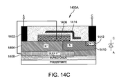
- FIG. 14C is a cross-sectional view depicting at least a portion of an alternative embodiment of an exemplary Schottky diode
- FIG. 15 is a cross-sectional view depicting at least a portion of an exemplary Schottky diode, according to a third embodiment of the invention.
- FIG. 15A is a cross-sectional view depicting the gate trench structure of FIG. 15 ;
- FIG. 15B is a cross-sectional view depicting at least a portion of another embodiment of an exemplary Schottky diode
- FIG. 15C is a graph illustrating a change of the conduction current for an embodiment of an exemplary Schottky diode
- FIGS. 16 and 17 are top plan and cross-sectional views, respectively, depicting at least a portion of an exemplary resistor structure in a serpentine layout, according to an embodiment of the invention.
- FIG. 18 is a cross-sectional view depicting at least a portion of an exemplary capacitor structure, according to an embodiment of the invention.
- FIG. 19 is a cross-sectional view depicting at least a portion of an exemplary P-channel MOSFET, according to an embodiment of the invention.
- FIGS. 20A through 20F are cross-sectional views depicting an exemplary BiCMOS process flow, according to an embodiment of the invention.
- FIGS. 21A through 21E are cross-sectional views depicting at least a portion of an exemplary BiCMOS process flow for integrating two power devices on the same SOI substrate, according to an embodiment of the invention.
- FIGS. 22A-22C illustrate the electric field distribution between gate and drain regions for various shielding structures
- FIG. 23 is a cross-sectional view illustrating a chip-scale assembly
- FIGS. 24A and 24B are cross-sectional views depicting at least a portion of an example N-channel LDMOS transistor formed on a bulk semiconductor substrate, according to an embodiment of the invention.
- FIGS. 25A and 25B are cross-sectional views depicting at least a portion of an example N-channel LDMOS transistor formed in and/or on an epitaxial layer which is formed on a bulk semiconductor substrate, according to an embodiment of the invention
- FIG. 26 is a cross-sectional view depicting at least a portion of an example N-channel LDMOS transistor formed on a bulk semiconductor substrate, according to another embodiment of the invention.
- FIG. 27 is a cross-sectional view depicting at least a portion of an example N-channel LDMOS transistor formed in and/or on an epitaxial layer which is formed on a bulk semiconductor substrate, according to another embodiment of the invention.
- Embodiments of the invention will be described herein in the context of illustrative power management circuits and semiconductor fabrication methods for forming one or more components suitable for use in the illustrative power management circuits. It should be understood, however, that embodiments of the invention are not limited to the particular circuits and/or methods shown and described herein. Rather, embodiments of the invention are more broadly related to techniques for fabricating an integrated circuit in a manner which achieves high-frequency performance for a variety of power management applications, such as, for example, a DC/DC power converter, and advantageously reduces the physical size and cost of external components which may be used in conjunction with embodiments of the invention, such as, for example, an output filter, among other benefits.
- MOSFET metal-insulator-semiconductor field-effect transistor
- MOSFET is, for example, intended to encompass semiconductor field-effect transistors that utilize an oxide material as their gate dielectric, as well as those that do not.
- metal in the acronyms MOSFET and MISFET
- a MOSFET and/or MISFET according to embodiments of the invention are also intended to encompass semiconductor field-effect transistors having a gate formed from a non-metal, such as, for instance, polysilicon.
- CMOS complementary metal-oxide-semiconductor
- embodiments of the invention are fabricated in a silicon wafer
- embodiments of the invention can alternatively be fabricated on wafers comprising other materials, including but not limited to gallium arsenide (GaAs), gallium nitride (GaN), indium phosphide (InP), cadmium selenide (CdSe), cadmium telluride (CdTe), zinc sulfide (ZnS), etc.
- GaAs gallium arsenide
- GaN gallium nitride
- InP indium phosphide
- CdSe cadmium selenide
- CdTe cadmium telluride
- ZnS zinc sulfide
- the illustrative power stage can be monolithically integrated in a power management circuit architecture as shown in FIG. 1 , wherein the control circuitry 102 , driver stage 104 and power switches 106 , 108 are all fabricated on the same IC chip 100 .
- the control circuitry 102 , driver stage 104 and power switches 106 , 108 are all fabricated on the same IC chip 100 .
- an alternative partitioning of the power management circuit is advantageous and/or required.
- FIG. 2 is a block diagram illustrating an exemplary power stage comprising power management control circuitry 102 and a driver stage 104 implemented in a first IC 200 , and power switches implemented in individually packaged discrete IC devices, 202 and 204 , coupled with and external to the first IC.
- parasitic impedances primarily parasitic inductance
- interconnections 206 e.g., printed circuit traces, bond wires, ball grid array (BGA), etc.
- BGA ball grid array
- FIG. 3 is a block diagram illustrating at least a portion of an exemplary power stage 300 comprising power management control circuitry 302 implemented in a first IC 304 , and a driver stage 306 and power switches 308 and 310 implemented in a second IC 312 coupled with the first IC 304 , according to an embodiment of the invention.
- the partitioning of the power stage 300 as shown in FIG. 3 is applied, for example, to DC/DC converters and other circuits and subsystems with a power conversion larger than about 30 watts.
- the power stage 300 is partitioned into a control IC 304 , fabricated in a more complex digital VLSI (very large scale integration) technology process, and a power block 312 implemented as a multi-chip module (MCM) including the driver stage 306 , fabricated in an analog technology, and discrete power switches 308 and 310 integrated as bare dies in the MCM.
- MCM multi-chip module
- the MCM approach of FIG. 3 is used for power management systems for large power applications, e.g., for desktop computers.
- the module contains three separate dies: driver chip and two MOSFET power switches.
- Portable electronics puts a strong demand on miniaturization of the implemented subsystems (i.e., small volume), and on reducing power losses generated in power conversion stages.
- aspects of the invention provide a cost-effective technology solution allowing a monolithic integration of driver stages with power switches which enable a two-die solution according to the partition scheme shown in FIG. 3 . That is, the driver and FET power switches can be manufactured on the same die for medium power applications needed for battery operated portable electronics. There is presently no technology enabling such system partitioning for a power range higher than about five watts.
- a digital/analog process such as, for example, a BiCMOS technology
- a digital/analog process is developed with an aim to maximize integration density and speed of signal processing.
- Optional power switches which can be designed using existing doping profiles and process steps generally cannot achieve sufficient performance in a power management application.
- the reduction of transistor on-resistance and the reduction of switching power loss require a dedicated optimization of the doping structure and use of a tailored sequence of process steps. This is usually done in the design of discrete power switches only.
- the processing of discrete power switches does not allow a monolithic integration of different electronic components, including NFETs, PFETs, bipolar junction transistors, P-N junction and Schottky diodes, etc.
- Power management systems typically use power switches to perform a high-frequency chopping of the input power and use an output filter comprising inductors and capacitors to stabilize the output voltage under variable load conditions.
- the higher the switching frequency the better the power conversion performance, and smaller volume and cost of the required output filter.
- An increase in the switching frequency from about 1 megahertz (MHz) available today to about 5 MHz is desired but has not been achievable due to associated switching power losses in the power transistors used to implement the power switches which are attributable, at least in part, to device parasitic impedances (e.g., internal capacitance, inductance, and resistance).
- FIGS. 4 and 5 are cross-sectional views depicting discrete laterally diffused metal-oxide-semiconductor (LDMOS) transistors 400 and 500 , respectively, known in the art.
- LDMOS metal-oxide-semiconductor
- FIGS. 6 and 70 are cross-sectional views depicting LDMOS transistors 600 and 700 , respectively, formed on SOI substrates that are known in the art.
- Buried oxide beneath an active SOI layer e.g., 602 in FIGS. 6 and 702 in FIG. 7 ) lowers output capacitance (C OSS ) and strongly reduces a body diode volume, thereby reducing a diode stored charge (Q IT ) and related power loss during commutation (i.e., reversing bias across the transistor), compared to standard device structures. Both features reduce associated switching losses and enable an increase in the operating frequency of the device.
- the proposed transistors have not been broadly adapted for manufacturing of discrete and/or integrated power MOSFETs due to the increased cost of the product. Also, acceptance of this approach is impeded by problems with the long term reliability of the gate oxide at the gate side corner of the gate due to hot carrier injection (HCI) under avalanche condition.
- HCI hot carrier injection
- Power stages manufactured in accordance with aspects of the invention provide an enhanced power management solution for an input voltage range between about one volt and about ten volts (V), and an output current between about one ampere and about five amperes. Accordingly, the delivered power will cover a range roughly between three watts and 30 watts, although embodiments of the invention are not limited to this or any specific power range.
- embodiments of the invention described herein are based on a 20-volt BiCMOS technology implemented on SOI substrates with dielectric lateral isolation.
- the system partitioning presented in FIG. 3 is achieved as a two-die solution, according to embodiments of the invention.
- a chip-scale assembly i.e., chip-scale package (CSP) or wafer-level packaging (WLP)
- CSP chip-scale package
- WLP wafer-level packaging
- the higher cost of the power switches is leveraged by a lower cost of integrated drivers, and a strong reduction in volume and cost of filter components achieved by an increase in operating frequency.
- FIG. 8 is a cross-sectional view depicting at least a portion of an exemplary structure 800 which incorporates aspects according to an embodiment of the invention.
- the structure 800 may be fabricated using a BiCMOS process technology on an N-type or P-type substrate 801 .
- the structure 800 includes a combination of a buried well 802 which is locally implanted at the bottom of an active layer 804 and a plurality of trenches (i.e., trench stripes) 806 having sidewalls and bottom walls lined with gate oxide 808 , or an alternative dielectric, and filled with polysilicon material 810 , or an alternative conductive material.
- trenches i.e., trench stripes
- Trenches 806 are preferably formed as a group of parallel stripes which, when properly biased, affect a current flow therebetween (e.g., in the case of a FET or Schottky diode embodiment), or which function to increase a capacitance per area of the structure (e.g., in the case of a capacitor embodiment).
- the active layer 804 is formed as an N ⁇ region and the buried well 802 is formed as a P + well, although other embodiments may utilize an alternative doping scheme (e.g., N ⁇ region and N + buried well, or P ⁇ region and P + or N + buried well), as will become apparent to those skilled in the art given the teachings herein.
- the configuration of structure 800 beneficially allows integration of a variety of components, such as, for example, field-effect transistors (FETs), BJTs, PN diodes, Schottky diodes, resistors and capacitors.
- Each of the trenches 806 extends substantially vertically from a top surface 812 of the structure 800 , through the active layer 804 , and at least partially into the buried well 802 .
- the trenches 806 may extend through the buried well 802 , into the buried oxide layer 818 .
- the oxide lining 808 covering the sidewalls and bottom walls of the trenches 806 prevents direct electrical connection between the polysilicon material 810 filling the trenches and the buried well 802 .
- Polysilicon fill 810 is preferably used as a gate terminal which can be biased as in, for example, FET and Schottky diode embodiments.
- the buried well 802 has an important function in devices operative to sustain an applied blocking voltage, such as transistors or diodes. More particularly, a doping level, doping type and/or a location of the buried well 802 are configured in a manner which substantially pins (i.e., clamps) a breakdown voltage at the PN junction created between an upper right side (i.e., tip) of the buried well and an N ⁇ background doping of the active layer 804 . By selectively controlling one or more characteristics of the buried well 802 , an electric field distribution in the device is controlled.
- the trench stripes 806 having walls (i.e., sidewalls and bottom walls) lined with gate oxide 808 are placed between main terminals of the power devices formed therein.
- the term “main terminals” as used herein is intended to broadly refer to external connections to the device, such as, for example, source and drain terminals, in the case of an MOS device, or anode and cathode terminals, in the case of a diode.
- the trench gates stripes 806 are formed (e.g., etched) substantially in parallel to a current path in the illustrative embodiment shown in FIG. 8 .
- a conduction current flows in the N ⁇ active layer 804 between the gate trenches 806 and can be controlled (e.g., modulated) by an applied gate potential, in the case of, for example, a lateral Schottky diode.
- the trench gates 806 are operative to deplete or enhance a gate/body interface, controlling the current flow through an inversion channel formed in the device.
- Doped polysilicon material 810 filling the trenches is used to create a gate bus connecting the gate regions to a gate terminal in a third dimension (not explicitly shown).
- the polysilicon material 810 is preferably doped with phosphorous, with a doping concentration of greater than about 10 19 /cm 3
- the polysilicon material is preferably doped with boron having a doping concentration of about 10 19 /cm 3 .
- the top surface of polysilicon gate layer 810 is shown optionally covered by a layer of silicide material 814 (e.g., titanium silicide (TiSi) or tungsten silicide (WSi)) with low resistivity, which can be deposited thereon using a known silicide deposition process (e.g., chemical vapor deposition (CVD), sputter deposition, etc.).
- silicide material 814 e.g., titanium silicide (TiSi) or tungsten silicide (WSi)
- the silicide layer 814 which forms a polycide electrode in the structure 800 , reduces a gate resistance of the structure.
- narrow gate trenches 806 are formed underneath the polycide electrode 814 along a path of current flow in the active layer 804 . In this manner, the trenches 806 increase an effective gate width in the MOSFET structure 800 , among other advantages.
- the deep trench structure 816 is preferably used to create a lateral isolation region between integrated components.
- the deep trench structure 816 also referred to herein as a lateral isolation trench, can be formed, for example, by etching from the top surface 812 of the structure, through the active layer 804 , to a buried oxide layer 818 formed on the substrate 801 .
- the lateral isolation trench 816 can be filled with oxide, or a combination of oxide and polysilicon.
- An optional deep trench cut (i.e., etch), not explicitly shown, through the buried oxide layer 818 to the substrate 801 can be used as a substrate contact.
- This optional trench is preferably filled with doped polysilicon, or an alternative conductive material, to ensure good ohmic (i.e., low resistance) contact to the substrate 801 .
- a variety of electronic components can be created using an illustrative BiCMOS process flow, according to embodiments of the invention. Examples of some components which can be formed which incorporate aspects of the invention are described herein below with reference to FIGS. 9A through 19 .
- FIG. 9A is a cross-sectional view depicting at least a portion of an exemplary N-channel LDMOS transistor 900 , according to an embodiment of the invention.
- the LDMOS transistor 900 has reduced gate-to-drain capacitance (C gd ) in comparison to standard LDMOS devices, due at least in part to the effect of the gate shield layer.
- LDMOS transistor 900 shows a small impact of the reverse recovery of the body diode (Q rr ) due at least in part to reduced diode stored charge.
- Transistor 900 includes an integrated PN clamping diode (i.e., a diode formed by the end of the deep well 902 and the drain region) as an integral part of each active cell that pins the avalanche breakdown away from the gate oxide and close to the upper right corner of a buried P + well 902 . That is, under blocking condition, the avalanche impact ionization is localized between the tip of the buried well 902 and the corner of the drain contact region, within the volume of the active layer and away from the top and bottom oxide interfaces. This increases the avalanche ruggedness of the power transistor without causing any reliability issues. This transistor design minimizes the injection of hot carriers into oxides, improving the long term reliability of the power switch.
- PN clamping diode i.e., a diode formed by the end of the deep well 902 and the drain region
- FIG. 9B illustrates the trench gate 906 formed substantially vertically through a P-type body region 920 and into the buried P + well 902 formed at the bottom of the body region.
- the trench gate 906 has walls (i.e., sidewalls and bottom walls) lined with gate oxide 922 .
- a lateral isolation structure 924 which may be formed in manner consistent with the lateral isolation structure 816 shown in FIG.
- a P ⁇ handle wafer in SOI substrate gets depleted along a P ⁇ substrate/buried oxide interface, which reduces an output capacitance, C oss , of the MOSFET.
- the source and drain regions may be referred to generally as first and second source/drain regions, respectively, where “source/drain” in this context denotes a source region or a drain region.
- source/drain in this context denotes a source region or a drain region.
- LDMOS device which is generally not bidirectional, such source and drain designations may not be arbitrarily assigned.
- the buried well 902 like the buried well 802 shown in FIG. 8 , has an important function, especially in devices operative to sustain an applied blocking voltage (e.g., transistors and diodes). More particularly, a doping level, doping type and/or a location of the buried well 902 are configured in a manner which substantially clamps the breakdown voltage at the PN junction formed between an upper right side of the buried well and an N ⁇ background doping of an active layer 904 in the device. By selectively controlling one or more characteristics of the buried well 902 , an electric field distribution in the device is controlled.
- an electric field distribution in the device is controlled.
- the device can be advantageously arranged such that a maximum electric field is distributed between the upper right corner of the buried well 902 and a right bottom corner of a drain contact region 910 .
- a clamping PN diode is integrated within the device which keeps hot carriers, generated by avalanche impact ionization, far away from a top silicon/oxide interface. This feature increases an ability of the device to absorb avalanche energy without creating reliability issues in the device.
- LDMOS transistors 600 and 700 shown in FIGS. 6 and 7 are pushed into avalanche, impact ionization will take place at a bottom corner of the gate covering a lightly doped drain (LDD) region in the device, and the injection of hot carriers into a gate oxide in the device will often result in reliability issues, as are known to those skilled in the art. For at least this reason, conventional LDMOS structures on SOI are not suitable for use as power switches.
- the LDMOS structure formed in accordance with one or more aspects of the invention is well-suited for use in a power switching application.
- LDMOS transistor 900 includes a shield field plate 912 , or alternative shielding structure, which, in this embodiment, is formed as a lateral extension of a conductive layer lining the source trench contact walls, overlaps a gate (e.g., polysilicon structure) 914 and comes into close proximity with an oxide interface along the N drain extension region (i.e., LDD region) 908 .
- the conductive layer is preferably deposited as a titanium (Ti)/titanium nitride (TiN) stack, but may be also formed of other materials, such as, for example, a titanium (Ti)/tungsten silicide (WSi) film.
- the source trench is formed on the left-hand side of the LDMOS transistor 900 , having side walls and a bottom wall lined with gate shield plate 912 and filled with top metal.
- the shield 912 functions primarily as a field plate, distributing (e.g., stretching) an electric field distribution along a top oxide interface away from an edge (e.g., bottom right corner) of the gate 914 nearest the drain, and also as a shield that helps to reduce gate-to-drain capacitance, C gd (so called Miller capacitance, which determines the switching speed of the transistor), at a positive bias of the drain and further improves gate oxide reliability.
- C gd gate-to-drain capacitance
- Miller capacitance which determines the switching speed of the transistor
- Drain and source contacts 910 and 916 are formed as metal-filled vias reaching a patterned top metal layer (not explicitly shown, but implied) and form drain (D) and source (S) terminals, respectively, of the LDMOS transistor 900 . Depleting the lightly doped drain extension region ( 908 ) also at a positive bias applied to the drain contact 910 also helps reduce C gd .
- the silicide layer 918 is preferably formed using a known deposition process (e.g., CVD, sputtering, etc.).
- FIG. 10 is a cross-sectional view depicting at least a portion of an exemplary N-channel LDMOS transistor 1000 , according to another embodiment of the invention.
- This LDMOS transistor 1000 is designed as a simplification of the LDMOS transistor 900 shown in FIGS. 9A and 9B .
- one simplification in the fabrication of LDMOS transistor 1000 compared to LDMOS transistor 900 shown in FIGS. 9A and 9B , comprises removal of the gate trenches ( 906 in FIGS. 9A and 9B ).
- a primary impact on the performance of the MOSFET 1000 is a smaller gate width per unit area, which increases on-resistance, R ON , of the resulting device. This can be leveraged by making the channel length shorter, as the alignment restriction related to an overlap of the gate polysilicon over gate trench endings is removed.
- Other features and characteristics of the MOSFET transistor 1000 remain essentially the same as for LDMOS transistor 900 .
- FIG. 10A illustrates an alternative embodiment of the LDMOS transistor 1000 of FIG. 10 .
- this embodiment includes a modification to extend the breakdown voltage above 20V.
- a narrow stripe of thicker oxide 1016 is introduced between the gate and the drain terminals. This allows the gate shield 1012 to form a two-step field plate (i.e., raised step portion 1014 is added), which further improves the electric field distribution.
- FIGS. 22A-22C show the electric field distribution between gate and drain regions in various configurations.
- FIG. 22A shows the electric field distribution between gate and drain regions without the effect of the field plate.
- the high electric field peak at the corner of the gate allows the injection of hot carriers into the gate oxide, which reduces the reliability of the transistor.
- FIG. 22B shows that the field plate formed by the gate shield layer, in a transistor designed for 20V breakdown, eliminates this critical electric field.
- FIG. 22C shows that the introduction of a thicker oxide stripe enables a two-step field plate contour that pushes the peak electric field away from the gate corner.
- this structure is preferably used in transistors designed for a breakdown voltage higher than 20V.
- FIG. 11 is a cross-sectional view depicting at least a portion of an exemplary low voltage signal MOSFET 1100 , according to an embodiment of the invention.
- the MOSFET 1100 includes a P body region 1102 and an N drain region 1104 , which can be used to form other circuit components, as will be described in further detail below.
- the P + buried well is not directly connected with the source terminal, as it is in the exemplary MOSFET 1000 shown in FIG. 10 , but rather is connected with a separate bulk (B) terminal. This configuration allows a voltage potential to be applied to the buried well that is different from the voltage potential applied to the source terminal.
- the MOSFET 1100 is formed by a further simplification of the illustrative transistor 1000 shown in FIG. 10 .
- MOSFET 1100 has reduced high-voltage capability and reduced avalanche ruggedness, but these features are generally more important for power switching applications.
- the transistor is designed to a target breakdown voltage specification between 12V and 60V.
- These MOSFETs are optimized for application as power switches with minimized conduction and switching power losses in low voltage power management systems.
- the embodiments described herein enable an increase of the switching frequency of DC/DC converters from 1.5 MHz to 5 MHz while implementing the integrated scheme of FIG. 3 .
- FIG. 12A a cross-sectional view depicts at least a portion of an exemplary SOI bipolar junction transistor (BJT) 1200 , according to an embodiment of the invention.
- BJT 1200 is formed as a modification of the MOSFET transistor 1000 shown in FIG. 10 .
- a former body region 1102 of the MOSFET 1100 shown in FIG. 11 is used as a base region 1201 of the BJT 1200 .
- the source trench contact has been removed. Instead, an emitter contact 1202 is cut across the base region 1201 to make a connection between a deep P + layer 1204 and the polycide structure (i.e., silicided polysilicon).
- connection 1252 between the deep P + layer 1204 and the polycide structure 1254 is formed as small spots (i.e., contacts) by interrupting the emitter contact 1202 (e.g., between fingers) along the finger layout.
- the connection 1252 in this embodiment, is formed as a lateral extension of the titanium (Ti)/titanium nitride (TiN) layer (in a manner similar to the field plate 912 shown in FIG. 9 ) and overlaps the polycide structure 1254 .
- These contacts are preferably placed at prescribed intervals along the polycide stripe (e.g., the polycide region which, in the case of a MOSFET, would be the gate patterned as a stripe, and is used to build a base bus contact), and the polycide layer is used to create a base bus with low resistivity.
- the polycide material as the current bus contacting the base region to the base terminal assures low base resistance, which improves the switching performance of the transistor.
- FIG. 12C illustrates a BJT embodiment 1250 A where a base contact 1256 is formed partially in a trench region formed in the active region and in electrical contact with the connection 1252 .
- connection 1252 A does not directly contact the polycide base but rather is spaced therefrom.
- a button-like contact 1258 is provided and contacts both the upper surface of the polycide base and the supper surface (and optionally side surface) of connection 1252 A.
- One or more of these button contacts 1258 can be spaced (in a third dimension along the base polycide stripe and interleaved with the emitter contact) to make contact between the polycide base structure with the deep P+ well 1204 and base contact 1256 via the connection layer 1252 A.
- the initial high-voltage capability and the avalanche ruggedness of the MOSFET transistor are preserved using this BJT configuration.
- the PN junction created between the tip of the deep P+ well and the collector region acts as the clamping diode.
- the PN clamping diode of the BJT pins the area of the avalanche breakdown within the volume of the silicon layer, confining hot carriers generated by avalanche impact ionization to this location.
- the BJT includes a MOS channel underneath the polycide stack, which creates a MOSFET structure in parallel with the bipolar transistor. If the positive bias applied to the BJT-base terminal is larger than the threshold voltage of the MOSFET, then the collector current is increased by the electron current flowing through the MOS channel, which improves the gain (( 3 ) of the BJT.
- a shield structure as discussed in connection with other embodiments described herein may also be incorporated into this design to improve the breakdown/reliability performance of the BJT device.
- the NPN BJT transistor structure shown in FIG. 12A can be converted into a PNP BJT by reversing the polarity of the implanted dopant regions.
- the basic MOSFET structure can be adapted to provide power diodes. Unlike conventional power PN diodes designed in a VLSI technology, the power PN diodes described herein exhibit avalanche ruggedness. Moreover, the basic MOSFET structure can be adapted to provide Schottky diodes, which are typically not in the designer's VLSI component toolbox. The structure disclosed herein increases the flexibility of the power management IC design by implementation of PN and Schottky diodes able to sustain the full supplied voltage. These diodes exhibit unique avalanche ruggedness when voltage spikes in the supply voltage rail drive the circuit beyond the allowed maximum blocking voltage value. These proposed diodes are compatible with the process flow disclosed for the SOI-MOSFETs and are straightforward modifications of that structure.
- FIG. 13 is a cross-sectional view depicting at least a portion of an exemplary PN diode 1300 , according to an embodiment of the invention.
- the PN diode 1300 is obtained as a modification of the exemplary MOSFET transistor 1000 shown in FIG. 10 .
- the N+ source region has been omitted, and the PN junction used to form the diode 1300 is created by a junction of the former P body 1102 and N drain 1104 .
- An anode (A) terminal is formed having a trench contact 1302 adapted for electrical connection with the P body 1102 .
- a cathode (C) terminal is adapted to provide electrical connection with N drain 1104 of the diode. The initial high-voltage capability and the avalanche ruggedness of the MOSFET structure are preserved.
- FIG. 13A is a cross-sectional view depicting at least a portion of an exemplary embodiment of a PN diode 1300 A, according to an alternative embodiment.
- the PN diode 1300 A is identical to the PN diode 1300 except for the modified trench contact 1302 A, which extends to at least partially overlap the gate to provide a shielding structure including a field plate, as described above in connection with FIGS. 9A and 10 .
- the PN diode of FIG. 13A preserves the full voltage blocking capability of the LDMOS structure by the presence of the deep P + well placed along the active layer interface to the buried oxide.
- the avalanche impact ionization is localized between the tip of the buried well and the corner of the cathode contact region, within the volume of the active layer and away from top and bottom oxide interfaces.
- This design of the diode minimizes the injection of hot carriers into oxides improving the long term reliability of the power device.
- the PN junction which is created by the end of the deep P + well and the cathode region, acts as a clamping diode as an integral part of each active cell of the diode.
- the avalanche breakdown defined by this clamping diode is pinned within the volume of the Silicon material increasing the avalanche ruggedness of the power device.
- the integrated shielding structure reduces the capacitive coupling between the gate and cathode terminals and serves as a field plate stretching out the electric field distribution along the top oxide interface with the Ldd region.
- the electric field peak appearing at the cathode side corner of the gate stack is now split between the gate corner and the end of the field plate, reducing the electric field peak value and inhibiting early injection of hot carriers into the oxide.
- the polycide gate and the deep P+ well can be connected to the anode terminal in a third dimension.
- the polycide gate can be connected to the anode and deep P+ well via a button-like contact 1304 extending through the conductive layer/gate shield 1302 A that makes electrical contact with both the polycide of the gate structure and with the conductive layer/gate shield 1302 A (e.g., by being formed partly on the top surface of the conductive layer 1302 A).
- buttons contacts 1304 can be spaced (in a third dimension) to make contact to the gate polycide in prescribed intervals (e.g., in a finger layout) along the polycide stripe rather than interrupting the shielding structure 1302 A with a continuous contact.
- FIG. 13C illustrates an alternative approach to coupling the gate polycide to the anode and deep P+ well.
- the anode trench contact 1302 B has a lateral extension that (like the extension shown in FIG. 12B ) that extends to connect the gate polycide to the anode and deep P+ well.
- This extension 1302 B also extends to form the shielding structure with field plate as described above in connection with the embodiment FIG. 13B .
- the gate bus can be configured as a terminal separate from the anode, and the two can be shorted together externally. This approach may provide for simpler processing in some embodiments.
- TMBS structure Trench-MOS-Barrier-Schottky
- the electrical shield of the Schottky contact enables the use of the higher doping of the semiconductor (lower Vf) without any deterioration of the blocking capability.
- the leakage current of a TMBS diode has flat voltage characteristics up to the breakdown voltage defined by the PN junction present in a neighbor cell.
- U.S. Pat. No. 7,745,846 discloses a Schottky diode integrated as a dedicated cell in an LDMOS transistor structure.
- the structure has a vertical current flow towards the drain contact at the back side of the wafer.
- the electrical shielding of the Schottky contact formed between the top metal and the LDD-1 region is achieved by the blocking impact of the gate and P-buffer regions.
- the forward I-V characteristics of the Schottky diode can be influenced by the gate potential.
- the integrated Schottky diode has the same blocking voltage capability as the parent LDMOS transistor. No comparable Schottky diodes are proposed in the art for power management ICs.
- FIG. 14A is a cross-sectional view depicting at least a portion of an exemplary Schottky diode 1400 , according to an embodiment of the invention.
- the Schottky diode 1400 is formed as a modification of the PN diode 1300 shown in FIG. 13 .
- the anode trench contact 1302 is omitted, along with the P body region 1102 (see FIG. 13 ), allowing a Schottky barrier to be created at an interface between the anode contact (metal) 1402 and an N ⁇ active layer 1404 .
- the Schottky barrier is stabilized by a two-step rapid thermal annealing (RTP at 650° C.
- RTP rapid thermal annealing
- the top polycide layer 1406 and deep P + well 1408 are electrically connected to the anode (A) terminal and induces a pinching of the electric field distribution under an applied blocking bias of the cathode (C) terminal.
- the shielding effect keeps leakage current in the diode 1400 low in the full range of the blocking voltage (e.g., about 12 volts to about 20 volts, although the invention is not limited to any specific voltage or range of voltages).
- the value of the leakage current in the diode will be a function of doping characteristics of the N ⁇ active region 1404 at the Schottky contact, as will be known by those skilled in the art. (See, e.g., U.S. Pat. No. 5,365,102, the disclosure of which is incorporated by reference herein in its entirety.). Shielding of the Schottky contact enables a higher doping of the semiconductor at the Schottky interface, as discussed below in connection with FIG. 14B , and improves the electrical performance of the diode.
- connection of the deep P + well 1408 and the polycide structure 1406 with the anode contact 1402 can be formed in a manner consistent with the connection 1252 shown in FIG. 12B for the illustrative BJT device 1250 .
- the connection between the deep P + layer 1408 and the polycide structure 1406 is preferably formed as small spots by interrupting the anode contact 1402 along a finger layout.
- the connection in this embodiment, is formed as a lateral extension of the titanium (Ti)/titanium nitride (TiN) layer (not explicitly shown in FIG. 14A , but implied in a manner similar to the connection 1252 shown in FIG. 12B ) and overlaps the polycide structure 1406 .
- These contacts are preferably placed at prescribed intervals along the polycide stripe (e.g., the polycide region which, in the case of a MOSFET, would be the gate patterned as a stripe), and the polycide layer is used to create a low resistivity shielding structure which is operative to shield the Schottky contact against any high electric field under blocking conditions, as previously stated.
- the polycide stripe e.g., the polycide region which, in the case of a MOSFET, would be the gate patterned as a stripe
- the polycide layer is used to create a low resistivity shielding structure which is operative to shield the Schottky contact against any high electric field under blocking conditions, as previously stated.
- FIG. 14C illustrates a cross-sectional view depicting at least a portion of an exemplary Schottky diode 1400 A, according to an alternative embodiment.
- the Schottky diode 1400 A is identical to the Schottky diode 1400 except for the inclusion of the shielding structure 1414 , which serves as both a gate shield and a field plate for the Schottky diode 1400 A.
- the connection of the deep P + well 1408 and the polycided gate structure 1406 with the anode contact 1402 can be formed in a manner consistent with the connection shown in FIG. 13B or 13C for the illustrative PN diode device 1300 A, or external connections can be made as dictated by the process.
- the shielding structure 1414 can also be incorporated into the Schottky diode structure shown in FIG. 14B .
- the initial high-voltage capability and the avalanche ruggedness of the MOSFET structure are preserved, as the blocking voltage is sustained by the device structure on the cathode (former drain) side of the top polycide electrode, and the avalanche breakdown is clamped by the PN junction at the upper right corner (i.e., tip) of the deep P + well 1408 .
- the deep well 1408 is preferably an implanted well with a maximum doping concentration close to the Si/buried oxide interface. In a preferred embodiment, the maximum doping concentration is in the range of about 5e16 cm ⁇ 3 and 5e17 cm ⁇ 3 , and the doping profile is configured to slope down towards the surface.
- the invention is not limited to a specific doping concentration or profile of the deep well 1408 .
- the PN junction in this embodiment, is formed by the deep P + well 1408 , N ⁇ active layer 1404 , N region 1410 and N + region 1412 toward the cathode terminal.
- FIG. 14B is a cross-sectional view depicting at least a portion of an exemplary Schottky diode 1450 , according to another embodiment of the invention.
- the Schottky diode 1450 is essentially the same as the Schottky diode 1400 depicted in FIG. 14A , except that an additional N region 1452 is formed in the N ⁇ active layer 1404 , proximate an upper surface of the N ⁇ active layer, in a manner similar to N region 1410 .
- An advantage of the Schottky diode 1450 compared to Schottky diode 1400 shown in FIG. 14A , is that the forward voltage drop of the Schottky diode 1400 depicted in FIG.
- N implant region 1410 can be reduced by increasing the doping concentration of the N ⁇ active layer 1404 proximate the Schottky contact. In a preferred embodiment, this is achieved by extending the N implant region 1410 at the cathode side of the polysilicide region to the region under the anode (A) contact 1402 , shown as N region 1452 in FIG. 14B .
- an important benefit according to one or more embodiments of the invention is the inclusion of the deep well which is configured to clamp the breakdown voltage away from the silicon/oxide interface. This arrangement advantageously enables the structure to absorb avalanche energy without experiencing reliability issues. Additional structures according to other embodiments of the invention incorporate a similar configuration of the drain region, thus inheriting the avalanche ruggedness of the parent MOSFET design shown, for example, in FIGS. 9A and 9B .
- FIG. 15 is a cross-sectional view depicting at least a portion of an exemplary Schottky diode 1500 , according to another embodiment of the invention.
- Schottky diode 1500 is formed as a modification of the illustrative Schottky diode 1400 depicted in FIG. 14A .
- gate trenches 1502 are formed in the device, preferably along a current flow path in the N ⁇ mesa region (i.e., active layer) 1404 underneath a polycide electrode 1504 formed on an upper surface of the active layer of the diode 1500 .
- the gate trench structure 1502 additionally improves the shielding effect of the Schottky contact against the blocking voltage applied to the cathode (C) terminal.
- the gate electrode is decoupled from an anode (A) terminal and can be used to further modify a conduction path between the gate trenches 1502 .
- the anode terminal is connected to the deep P + well 1408 in a third dimension, which is not explicitly shown but is implied.
- the Schottky diode 1500 may be referred to herein as a switched Schottky diode and represents a new type of power device, according to an embodiment of the invention.
- FIG. 15A is a cross-sectional view depicting the trench structure of the switched Schottky diode device of FIG. 15 in more detail.
- the current flows under conduction condition between the gate trenches 1502 from the anode (source) contact to the cathode (drain) region. If the trench width is smaller than the width of the N ⁇ mesa region (i.e., active regions 1404 ) between the trenches 1502 , then the effective gate width per active cell is increased.
- the increase of the gate width corresponds to an increase of the transconductance of the MOSFET, and respectively to a reduction of the on-resistance of the transistor. As shown in FIGS.
- the gate trenches are implemented in the SOI-Schottky diode structure to further intensify the shielding effect by combination of vertical and lateral depletion of the N ⁇ layer 1404 .
- the gate region can be accessed as a third terminal to turn on and off the lateral depletion effect by applying a corresponding bias to this electrode.
- the anode terminal can be connected to the deep P+ well 1408 in the third dimension as discussed above in connection with other embodiments.
- Lateral isolation regions 1514 which may comprise an oxide or other dielectric material, are formed in the diode structure 1500 to electrically isolate the diode from other circuit components on the die.
- FIG. 15B illustrates an alternative embodiment of a switched Schottky diode 1500 A.
- the switched Schottky diode 1500 A is essentially the same as the switched Schottky diode 1500 depicted in FIG. 1 , except that an additional N implant region 1552 is formed in the N ⁇ active layer 1404 , proximate an upper surface of the N ⁇ active layer, in a manner similar to N region 1510 . That is, the active layer is doped to a higher N dopant concentration in the vicinity of the Schottky contact while keeping the doping of the active layer between the gate trenches 1502 at the original lower N ⁇ level.
- An advantage of the switched Schottky diode 1500 A compared to switched Schottky diode 1500 shown in FIG. 15 , is that the forward voltage drop (Vf) of the Schottky diode 1500 depicted in FIG. 15 can be reduced by increasing the doping concentration of the N ⁇ active layer 1404 proximate the Schottky contact, and the shielding effect remains unaffected. In a preferred embodiment, this is achieved by extending the N implant region 1510 at the cathode side of the polysilicide region to the region under the anode (A) contact, shown as N region 1552 in FIG. 15B . While in known devices such as disclosed in U.S. Pat. No.
- the forward characteristics could be modified by the gate-to-anode bias applied to the gate electrode, the diode structure from FIG. 15B exhibits a change of the conduction current by four orders of magnitude when turning on and off the gate bias, as illustrated in FIG. 15C .
- This switched Schottky diode may be called a ⁇ -Switch due to the gate trench structure cross-section illustrated by FIG. 15A .
- a gate shield structure as discussed in connection with other embodiment may also be incorporated into this design to improve the breakdown/reliability performance of the device.
- FIGS. 16 and 17 are top plan and cross-sectional views, respectively, depicting at least a portion of an exemplary resistor structure 1600 in a serpentine layout, according to an embodiment of the invention.
- the resistor path 1602 is defined by an N ⁇ region 1604 between gate trenches 1606 , which is connected to N + contact regions 1608 and 1610 on both ends of the serpentine.
- One of the N + contact regions, e.g. 1608 includes a trench contact 1612 to a deep P + well 1603 (not explicitly shown in FIG. 16 , but shown in FIG. 17 as well 1702 ).
- the P + well 1603 isolates the N ⁇ resistor path 1602 from a bottom, as shown in the cross-sectional view of FIG. 17 . As shown in FIG.
- buried P + deep well 1702 is operative to electrically isolate the resistor formed by the N ⁇ region between the trenches.
- Lateral isolation regions 1614 which may comprise an oxide or other dielectric material, are formed in the resistor structure 1600 to electrically isolate the resistor from other circuit components on the die.
- a cross-sectional view depicts at least a portion of an exemplary capacitor structure 1800 , according to an embodiment of the invention.
- the capacitor structure 1800 can have a serpentine layout similar to the resistor structure 1600 shown in FIG. 16 , or it may comprise multiple parallel stripes formed by the trenches 1802 .
- Capacitor electrodes 1802 are formed by the polysilicon fill in the gate trenches and by the deep N + well 1804 at the bottom of the active layer 1806 . Both regions are connected to terminals at ends of the serpentine layout, not explicitly shown but implied.
- Lateral isolation regions 1808 which may comprise an oxide or other dielectric material, are formed in the capacitor structure 1800 to electrically isolate the capacitor from other circuit components on the die.
- FIG. 19 is a cross-sectional view depicting at least a portion of an exemplary P-channel MOSFET 1900 , according to an embodiment of the invention.
- the MOSFET 1900 is formed as a modification of the N-channel MOSFET 900 shown in FIG. 9 , wherein a polarity type of the material used to dope the body (P body in FIG. 9 ), as well as source and drain regions, have been reversed to create a P-channel LDMOS transistor.
- the implants dedicated to form a P-channel MOSFET in parallel to the N-channel transistor increases the mask count compared to the process used to make the N-channel LDMOS transistor 900 only, as will be known by those skilled in the art.
- one simplification in the fabrication of LDMOS device 1900 comprises removal of the gate trenches 1902 .
- a primary impact on the performance of the resultant MOSFET is a smaller gate width per unit area, which increases on-resistance, R ON , of the resulting device. This can be leveraged by making the channel length shorter, as the alignment restriction related to an overlap of the gate polysilicon over gate trench endings is removed.
- the exemplary electronic components depicted in FIGS. 9 through 19 can be used to build a BiCMOS circuit including power switches, diodes, and some associated circuitry.
- the BiCMOS process flow includes a basic mask set allowing manufacturing of components presented in FIGS. 9 through 17 , and an additional mask subset allowing the component portfolio to include the structures shown in FIGS. 18 and 19 .
- the phrase “basic mask set” is defined broadly to refer to a minimum number of mask levels required to fabricate a set of devices based on an NFET structure according to embodiments of the invention.
- FIGS. 20A through 20F cross-sectional views, collectively, depict an exemplary BiCMOS process flow, according to an embodiment of the invention.
- the process flow uses a basic mask set for manufacturing circuit components based on modifications of the N-channel LDMOS device shown in FIG. 9 , as described herein above.
- the process is based on an SOI substrate with a P ⁇ handle wafer, and an N ⁇ active layer.
- an illustrative process flow in accordance with an embodiment of the invention includes the following primary steps:
- lateral dielectric isolation also referred to as lateral trench isolation (LTI)
- LTI mask first mask step
- body mask perform body diffusion, for example with a dedicated thermal anneal, as shown in FIG. 20C ;
- Implant phosphor or arsenic, or an alternative dopant to create a lightly doped drain (LDD) extension 2016 at the other edge of the polycide layer 2012 , opposite the edge used to form the body region 2014 , using a sixth mask step (LDD mask), as shown in FIG. 20C ;
- LDD mask lightly doped drain
- Source/drain mask Source/drain mask
- Etch a shallow source contact trench 2026 using an eighth mask step (trench contact mask), and implant BF 2 through the trench bottom (plug implant) to assure a good ohmic contact to the body and deep P + regions, as shown in FIG. 20E ;
- a silicide film 2028 e.g., Ti/WSi x or Ti/TiN
- a silicide film 2028 e.g., Ti/WSi x or Ti/TiN
- a silicide e.g., TiSi x
- Such a contact formation methodology is well known to those skilled in the art;
- ILD interlayer dielectric film
- CMP chemical-mechanical polishing step
- N-channel LDMOS (NFET) transistor requires eleven mask levels (i.e., steps). The number of mask levels can be reduced to ten if the gate trench processing is omitted, as noted above.
- An optional mask can be used to create an electrical contact to the substrate by etching a deep trench through the active layer and the buried oxide, and filling it with oxide and doped polysilicon.
- PFET P-channel MOSFET
- dedicated additional implants are made using the following mask levels: P-BL, P-POLYDOP, P-BODY, P-LDD, P-S/D, and P-CONT, where P-BL refers to a P-type doping of the buried layer, and P-POLYDOP refers to a mask level enabling P + doping of Polysilicon for the PFET devices.
- P-BL refers to a P-type doping of the buried layer
- P-POLYDOP refers to a mask level enabling P + doping of Polysilicon for the PFET devices.
- an additional N-POLYDOP mask level is used for the N+ doping of polysilicon for NFET devices.
- the complete mask set in the exemplary BiCMOS process includes a maximum of 18 to 20 levels.
- This process flow allows a design of all the exemplary electronic components shown in FIGS. 9 through 19 which may be used to manufacture a power IC.
- the process flow using the basic mask set needed to manufacture diode power devices described herein is the same as discussed above for the BiCMOS technology.
- the process is based on an SOI substrate with a P ⁇ handle wafer, and an N ⁇ active layer in the case of an Nch MOSFET.
- This process flow can include the following main steps when forming diode structures disclosed herein:
- Lateral dielectric isolation by etching a trench through the active layer, and fill it with oxide or a combination of oxide and polysilicon (LTI Mask);
- lightly doped drain (LDD) lightly doped drain extension
- Etch a shallow source (anode) contact trench (CONT Mask) and implant BF 2 through the trench bottom (plug implant) to assure a good ohmic contact to body and deep P + regions.
- silicide film e.g. Ti/TiN
- ILD interlayer dielectric film
- CMP chemical-mechanical polishing step
- Etch via openings to access anode, cathode, and gate contact areas (Via Mask). Fill vias with tungsten plugs (Ti/TiN/W) and apply CMP step to planarize the top surface again.
- An optional mask can be used to create an electrical contact to the substrate by etching a deep trench through the active layer and the buried oxide, and fill it with oxide and doped polysilicon.
- the basic mask set needed to manufacture a NPN transistor as discussed above can be used to form a power SOI BJT as described above in connection with FIG. 12A-12D , or 12 E as the case may be.
- the process is based on an SOI substrate with a P ⁇ handle wafer, and an N-active layer and can include the following main steps:
- Lateral dielectric isolation by etching a trench through the active layer, and fill it with oxide or a combination of oxide and polysilicon (LTI Mask).
- Implant boron to create a base region self-aligned to the edge of the polycide layer (BODY Mask).
- Perform base diffusion with a dedicated thermal anneal e.g., 1000° C. for 60 min to drive the implant under the whole length of the base/gate.
- LDD Mask Implant phosphorous or arsenic to create a lightly doped collector extension (similar to the LDD in the LDMOS structure)
- a silicide film e.g. Ti/TiN
- ILD interlayer dielectric film
- CMP chemo-mechanical polishing step
- Etch via openings to access emitter, collector and base contact areas (VIA Mask).
- An optional mask can be used to create an electrical contact to the substrate by etching a deep trench through the active layer and the buried oxide, and fill it with oxide and doped Polysilicon.
- a modified mask sub-set has to be used.
- additional implants are made using the following mask levels: P-BL, P-POLYDOP, P-BODY, P-LDD, P-S/D, and P-CONT.
- Both types of BJT transistors can be integrated within an SOI-BiCMOS process flow with maximum of 18 mask levels as discussed in the disclosure on SOI-BiCMOS. This process flow allows a design of variety of electric components which may be used to manufacture a power IC.
- the source and drain busses are placed at the opposite ends of the transistor active cells with a gate bus created by the polycide layer running along the center of the layout.
- the source and drain metal contacts have an interleaved finger structure, and their pitch equals the pitch of one active cell as shown in, for example, 9 A, 10 , 10 A, 11 or 19 .
- a predefined number of active cells is connected together through the bus structure into a large macro-cell with lateral dimension of a few hundred microns (e.g. 300 by 300 ⁇ m).
- This macro-cell approach enables a transistor layout scalable to a large area (e.g. 1 to 5 mm 2 ) by repetition and connection of the predefined macro-cells.
- the current bus stripes lead to terminal pad areas.
- a chip-scale assembly (CSP or WLP) is adopted, which has the advantage of a smaller product footprint and less parasitic components like package resistance and inductance
- the current bus structure 2308 (which corresponds to, for example, gate, drain and source top electrodes 2032 (or other contacts in the case of diode or BJT embodiments) is contacted to a ball contact 2306 through vias 2302 and a redistribution layer 2304 , as shown schematically in FIG. 23 .
- individual source, drain and gate busses can be connected to multiple source, drain and gate terminals, of multiple like or identical devices, thereby allowing those multiple devices to operate as a single macro-cell device.
- Multiple macro-cell devices can then be connected together to operate as one power device by, for example, the redistribution layer 2304 . That is, an individual contact 2306 can be connected to multiple source busses 2308 , for example, and the like for the gate and drain contacts 2306 .
- FIGS. 21A through 22E are cross-sectional views depicting at least a portion of an exemplary BiCMOS process flow for integrating two power devices on the same substrate, according to an embodiment of the invention.
- FIGS. 21A through 22E conceptually illustrate an exemplary process flow which utilizes the same process steps for integrating a power N-channel MOSFET and a power Schottky diode on a common SOI substrate.
- Other devices such as, for example, PN diodes and BJTs, can be fabricated within the same process step sequence.
- each of the active regions 2102 and 2104 in which devices will be formed comprise respective N ⁇ active regions 2106 separated by a lateral isolation trench 2108 , although the active regions 2106 may be of a different conductivity type in other embodiments.
- Lateral isolation trenches 2108 are used to separate other adjacent active regions 2106 for forming other devices and/or structures.
- the active regions 2106 are formed on a common buried oxide layer 2110 which in turn is formed on an N or P-type substrate 2112 . Buried P + wells 2114 are formed in the respective N ⁇ active regions 2106 , proximate an interface between the buried oxide layer 2110 and the active regions.
- a gate oxide layer 2120 is formed over the surface of the SOI structure.
- a layer of polysilicon 2122 is deposited on the gate oxide layer 2120 and patterned to form gate structures.
- a silicide layer 2124 is optionally deposited on the polysilicon gate structures 2122 .
- P body regions 2116 are formed by doping the active region 2106 over at least a portion of the buried wells 2114 , whereby the P implant used to form the P body regions is self-aligned to one edge of the polycide regions.
- N regions 2118 are also formed in the active layer 2106 .
- the N region 2118 is formed between the P body regions 2116 allocated to build a MOSFET structure (e.g., NMOS device 1000 shown in FIG. 10 ).
- MOSFET structure e.g., NMOS device 1000 shown in FIG. 10
- the same implantation step is used to form N regions 2118 in the structure of a Schottky diode, as previously shown in FIG. 14B .
- FIG. 21C shows doped N+ regions 2126 formed in P body regions 2116 and N regions 2118 .
- An oxide layer 2128 is formed over at least a portion of the upper surface of the SOI structure.
- trenches 2130 are formed substantially vertically through the oxide layer 2128 , the P body region 2116 , and contacting the buried P+ well 2114 .
- a silicide or titanium/titanium nitride layer 2132 is formed on sidewalls and a bottom wall of the trenches 2130 .
- the silicide layer 2132 lining the trenches 2130 contact the N + doped regions 2126 in the P body region 2116 .
- Shield field plates 2134 which in this embodiment are formed as lateral extensions of the silicide layers 2132 lining the trenches 2130 , overlap the gate structures and come into close proximity with an oxide interface along the N active region 2118 .
- FIG. 21E depicts the oxide layer 2136 etched to form contact trenches (i.e., vias), which are subsequently filled with a metal (e.g., aluminum), or an alternative conductive material, to form device contacts 2138 .
- a metal e.g., aluminum
- FIGS. 24A and 24B are alternative cross-sectional views depicting at least a portion of an example N-channel LDMOS transistor (“transistor”) 2400 formed on a bulk semiconductor substrate 2401 , according to an embodiment of the invention.
- the transistor 2400 includes: the bulk semiconductor substrate 2401 ; a buried well (i.e.
- the transistor 2400 additionally includes gate oxide 2422 and a lateral isolation region 2424 .
- the avalanche breakdown region 2413 is a region of the buried well 2402 that is in closest proximity to the drain contact 2410 .
- the avalanche breakdown region 2413 is labeled for illustration purposes only.
- the bulk semiconductor substrate 2401 is a P-type substrate (e.g. P, P + , or P ⁇ ). In other embodiments, the bulk semiconductor substrate 2401 is an N type substrate (e.g. N, N + , N ⁇ ). In still other embodiments, other doping schemes are used, as will become apparent to those skilled in the art given the teachings herein. In some embodiments, the N-type region 2404 is a region of the active region and has N ⁇ background doping.
- the active region 2102 and the active region 2104 of FIG. 21A are shown formed on the buried oxide layer 2110 .
- the active region of the transistor 2400 of FIG. 24A is formed directly on the bulk semiconductor substrate 2401 .
- the active region of the transistor 2400 includes the buried well 2402 , the N-type region 2404 , the source region 2405 , the drain region 2407 , the LDD extension region 2408 , and the body region 2420 .
- the transistor 2400 is fabricated using a BiCMOS process technology on the bulk semiconductor substrate 2401 .
- the fabrication process of the transistor 2400 is the same or similar to the fabrication process described in detail with reference to FIG. 20A through FIG. 20F and FIG. 21A through FIG. 21E , contrasted by the exclusion of a buried oxide layer.
- the gate trenches 2406 of the transistor 2400 include multiple trenches (i.e., trench stripes). Each trench has sidewalls and bottom walls lined with the gate oxide 2422 , or an alternative dielectric, and filled with polysilicon material, or an alternative conductive material which additionally forms the gate region 2414 .
- the polysilicon material is preferably doped with phosphorous, with a doping concentration of greater than about 10 19 /cm 3 .
- the polysilicon material is preferably doped with boron having a doping concentration of about 10 19 /cm 3 .
- the top surface of the gate region 2414 is shown optionally covered by the silicide layer 2418 .
- the silicide material e.g., titanium silicide (TiSi) or tungsten silicide (WSi)
- the silicide material has low resistivity.
- the silicide material is deposited onto the polysilicon material of the gate region 2414 using a known silicide deposition process (e.g., chemical vapor deposition (CVD), sputter deposition, etc.).
- the silicide layer 2418 which forms a polycide electrode in the transistor 2400 , reduces a gate resistance of the transistor 2400 .
- the gate trenches 2406 are preferably formed as a group of parallel stripes which, when properly biased, affect a current flow therebetween.
- the trenches of the gate trench 2406 are formed underneath the polycide electrode along a path of current flow in the active layer of the transistor 2400 . In this manner, the trenches of the gate trenches 2406 increase an effective gate width in the transistor 2400 , among other advantages.
- Each gate trench 2406 extends substantially vertically from the top of the active layer of the transistor 2400 (or top of the body region 2420 ), through the body region 2420 , and at least partially into the buried well 2402 . In some embodiments, each gate trench 2406 extends through the buried well 2402 .
- the gate oxide 2422 lining the sidewalls and bottom walls of the gate trenches 2406 prevents direct electrical connection between the polysilicon material filling the gate trenches 2406 and the buried well 2402 .
- the gate trenches 2406 are placed between the source contact 2416 and the drain contact 2410 and are formed (e.g., etched) to be substantially parallel to a current path.
- the gate trenches 2406 can deplete or enhance a gate/body interface, controlling the current flow through an inversion channel formed in the transistor 2400 .
- a conduction current flows in the body region 2420 between the gate trenches 2406 .
- the conduction current flows from the source contact 2416 , through the source region 2405 , through the body region 2420 between walls of the trench gates 2406 , through the LDD extension region 2408 , through the drain region 2407 and to the drain contact 2410 .
- the lateral isolation region 2424 can be formed, for example, by etching from the top surface 2415 of the transistor 2400 or from the top of the active layer of the transistor 2400 , through the active layer, to the bulk semiconductor substrate 2401 .
- the lateral isolation region 2424 can be filled with oxide, or a combination of oxide and polysilicon.
- An optional deep trench cut (i.e., etch), not explicitly shown, to the bulk semiconductor substrate 2401 can be used as a substrate contact.
- This optional trench is preferably filled with doped polysilicon material, or an alternative conductive material, to ensure good ohmic (i.e., low resistance) contact to the bulk semiconductor substrate 2401 .
- the silicide layer 2418 is formed on the gate region 2414 (a polysilicon gate structure), thereby forming a polycide layer (also referred to as silicided polysilicon).
- the silicide layer 2418 forms a gate bus leading to a gate terminal (G) located in a third dimension (not explicitly shown, but implied).
- the silicide layer 2418 is preferably formed using a known deposition process (e.g., CVD, sputtering, etc.).
- the source contact 2416 and the drain contact 2410 are formed as metal-filled vias reaching a patterned top or overlaying metal layer (not explicitly shown, but implied) and form the source terminal (S) and the drain terminal (D), respectively, of the transistor 2400 .
- the transistor 2400 includes an integrated PN clamping diode.
- the integrated PN clamping diode is formed by the buried well 2402 and the LDD region 2408 .
- the buried well 2402 is locally implanted at the bottom of the active region (below the body region 2420 ). This was illustrated in FIG. 20A , which shows a buried well 2004 implanted at the bottom of the active region 2002 .
- the clamping diode is as an integral part of each active cell (e.g. an active region fully or partially isolated from other active regions by lateral insulating structures such as the lateral isolation structure 2424 ).
- the clamping diode “pins” the avalanche breakdown away from the gate oxide 2422 and close to region of the buried well 2402 that is closest to the drain contact 2410 within the volume of the active layer.
- the region of the buried well 2402 that is closest to the drain contact 2410 is indicated as the avalanche breakdown region 2413 , located at the upper right corner of the buried well 2402 .
- Properties or characteristics of the buried well 2402 are configured, determined or selected in a manner which results in substantially clamping the breakdown voltage at the PN junction formed between the region of the buried well 2402 that is in closest proximity to the drain contact 2410 , as was described earlier.
- a distribution of an electric field in the transistor 2400 is affected.
- the transistor 2400 formed in accordance with one or more aspects of the invention is well-suited for use in a power switching application.
- the clamping diode increases the avalanche ruggedness of the transistor 2400 without causing any reliability issues. This transistor design minimizes the injection of hot carriers into oxides, improving the long-term reliability of the transistor 2400 .
- the transistor 2400 advantageously has a reduced gate-to-drain capacitance (C gd ) in comparison to standard LDMOS devices, due at least in part to the effect of the gate shield plate 2412 .
- the gate shield plate 2412 or an alternative shielding structure, is formed as a lateral extension of a conductive layer lining the walls of a trench for the source contact 2416 .
- the gate shield plate 2412 overlaps the gate region 2414 (e.g., polysilicon structure) and is proximate to an oxide interface along the LDD extension region 2408 .
- the trench for the source contact 2416 is formed on the left-hand side of the transistor 2400 , having side walls and a bottom wall lined with gate shield plate 2412 and is filled with top metal (e.g. of the source contact 2416 ).
- the conductive layer lining the walls of the trench for the source contact 2416 is preferably deposited as a titanium (Ti)/titanium nitride (TiN) stack, but may be also formed of other materials, such as, for example, a titanium (Ti)/tungsten silicide (WSi) film.
- the gate shield plate 2412 functions primarily as a field plate, distributing (e.g., stretching) an electric field along an interface with the top oxide region 2409 away from an edge (e.g., bottom right corner) of the gate region 2414 nearest the drain region 2407 .
- the gate shield plate 2412 also functions as a shield that helps to reduce gate-to-drain capacitance, C gd (so called Miller capacitance, which determines or affects the switching speed of the transistor 2400 ), at a positive bias of the drain region 2407 and further improves gate oxide reliability.
- C gd gate-to-drain capacitance
- the electric field peak appearing at the drain side corner of the gate region 2414 is split between the gate corner and the end of the gate shield plate 2412 , thereby reducing the electric field peak value and inhibiting early injection of hot carriers into the top oxide region 2409 .
- C gd can also be reduced by depleting the LDD extension region 2408 .
- the active region is formed directly on a bulk semiconductor substrate.
- the active region is formed in an epitaxial layer formed on a bulk semiconductor substrate.
- An epitaxial layer is a crystalline layer grown or deposited on a crystalline substrate (e.g. the bulk semiconductor substrate).
- Forming an epitaxial layer on the bulk semiconductor substrate can advantageously allow use of a heavily-doped semiconductor substrate in order to control the potential of the substrate, while maintaining a lightly-doped surface layer for which to manufacture active devices. Additionally, a buried layer can be implanted into the semiconductor substrate before the epitaxial layer is formed, resulting in a buried layer below the epitaxial layer.
- FIGS. 25A and 25B are alternative cross-sectional views depicting at least a portion of an example N-channel LDMOS transistor 2500 formed in an epitaxial layer 2511 which is formed on a bulk semiconductor substrate 2501 , according to an embodiment of the invention.
- the transistor 2500 includes: the bulk semiconductor substrate 2501 ; a buried well (i.e.
- the transistor 2500 additionally includes gate oxide 2522 and a lateral isolation region 2524 .
- the transistor 2500 includes the epitaxial layer 2511 .
- the active region of the LDMOS transistor 2500 is formed in the epitaxial layer 2511 that is formed on the bulk semiconductor substrate 2501 .
- the bulk semiconductor substrate 2501 is a P-type substrate (e.g. P, P + , or P ⁇ ).
- the bulk semiconductor substrate 2501 is an N type substrate (e.g. N, N + , N ⁇ ).
- other doping schemes are used, as will become apparent to those skilled in the art given the teachings herein.
- the epitaxial layer 2511 is shown as a separate layer, in some embodiments all or a portion of the active region of the LDMOS transistor 2500 is formed in the epitaxial layer 2511 .
- the active region of the LDMOS transistor 2500 is formed in the epitaxial layer 2511 and is not formed on the epitaxial layer 2511 .
- the active region of the LDMOS transistor 2500 is formed on the epitaxial layer 2511 and is not formed in the epitaxial layer 2511 .
- the active region of the LDMOS transistor 2500 is formed in and on the epitaxial layer 2511 .
- the epitaxial layer 2511 can be an N or P type epitaxial layer (N+/ ⁇ or P+/ ⁇ Epi-Layer) that is formed on the N or P type bulk semiconductor substrate 2501 .
- the active region includes the buried well 2502 , the N-type region 2504 , the source region 2505 , the drain region 2507 , the LDD extension region 2508 , and the body region 2520 .
- the bulk semiconductor substrate 2501 can be un-doped, or have a doping level that ranges from lightly doped to highly doped.
- the epitaxial layer 2511 is a P or P ⁇ epitaxial layer on a P or P + bulk semiconductor substrate ( 2501 ).
- the epitaxial layer 2511 is an N or N ⁇ epitaxial layer on a P or P + bulk semiconductor substrate ( 2501 ).
- the epitaxial layer 2511 can be un-doped, or have a doping level that ranges from lightly doped to highly doped.
- a lightly doped N ⁇ material can be used as the epitaxial layer 2511 to form the N-type region 2504 .
- a region of the N-type region 2504 can then be counter-doped to form the buried well 2502 .
- FIG. 26 is a cross-sectional view depicting at least a portion of an example N-channel LDMOS transistor (“transistor”) 2600 formed on a bulk semiconductor substrate 2601 , according to an embodiment of the invention.
- the transistor 2600 includes: the bulk semiconductor substrate 2601 ; a buried well (i.e.
- Deep Pt Deep Pt 2602 ; an N-type region 2604 ; a source region 2605 ; a drain region 2607 ; a LDD extension region 2608 ; an oxide region 2609 ; a drain contact 2610 ; a gate shield plate 2612 ; an avalanche breakdown region 2613 ; a gate region 2614 ; a top surface 2615 ; a source contact 2616 ; a silicide layer 2618 , and a body region (i.e. “P Body”) 2620 .
- the avalanche breakdown region 2613 is a region of the buried well 2602 that is in closest proximity to the drain contact 2610 .
- the avalanche breakdown region 2613 is labeled for illustration purposes only.
- the LDMOS transistor 2600 is designed as a simplification of the transistor 2400 shown in FIGS. 24A and 24B . As apparent from FIG. 26 , one simplification in the fabrication of the transistor 2600 , compared to the transistor 2400 shown in FIGS. 24A and 24B , includes removal of the gate trenches ( 2406 in FIGS. 24A and 24B ). A primary impact on the performance of the LDMOS transistor 2600 is a smaller gate width per unit area, which increases on-resistance, R ON , of the resulting device. This can be leveraged by making the channel length shorter, as the alignment restriction related to an overlap of the gate polysilicon over gate trench endings is removed. Other features and characteristics of the MOSFET transistor 2600 remain essentially the same as for LDMOS transistor 2400 .
- FIG. 27 is a cross-sectional view depicting at least a portion of an example N-channel LDMOS transistor (“transistor”) 2700 formed in and/or on an epitaxial layer 2711 which is formed on a bulk semiconductor substrate 2701 , according to another embodiment of the invention.
- the transistor 2700 includes: the bulk semiconductor substrate 2701 ; a buried well (i.e.
- Deep Pt Deep Pt 2702 ; an N-type region 2704 ; a source region 2705 ; a drain region 2707 ; a LDD extension region 2708 ; an oxide region 2709 ; a drain contact 2710 ; the epitaxial layer 2711 ; a gate shield plate 2712 ; an avalanche breakdown region 2713 ; a gate region 2714 ; a top surface 2715 ; a source contact 2716 ; a silicide layer 2718 , and a body region (i.e. “P Body”) 2720 .
- P Body body region
- the transistor 2700 is designed as a simplification of the LDMOS transistor 2500 shown in FIGS. 25A and 25B , the simplification including the removal of the gate trenches ( 2506 in FIGS. 25A and 25B ). Other features and characteristics of the LDMOS transistor 2700 remain essentially the same as for the LDMOS transistor 2500 .
- the fabrication process of the transistor 2400 , the transistor 2500 , the transistor 2600 and/or the transistor 2700 is the same or similar to the fabrication process described in detail with reference to FIG. 20A through FIG. 20F and FIG. 21A through FIG. 21E , contrasted by the exclusion of a buried oxide layer.
- the epitaxial layer 2711 is shown as a separate layer, in some embodiments all or a portion of the active region of the LDMOS transistor 2700 is formed in the epitaxial layer 2711 .
- MOSFET power devices include MOSFET power transistors, such as an N-channel LDMOS transistor, as described herein.
- the active region formed on a bulk semiconductor substrate includes MOSFET power transistors and integrated control circuitry.
- an active region formed in and/or on an epitaxial layer formed on a bulk semiconductor substrate includes MOSFET power transistors and integrated control circuitry.
- At least a portion of the embodiments of the invention may be implemented in an integrated circuit.
- identical die are typically fabricated in a repeated pattern on a surface of a semiconductor wafer.
- Each die includes at least one device described herein, and may include other structures and/or circuits.
- the individual die are cut or diced from the wafer, then packaged as an integrated circuit.
- One skilled in the art would know how to dice wafers and package die to produce integrated circuits. Integrated circuits so manufactured are considered part of this invention.
- An integrated circuit in accordance with embodiments of the invention can be employed in essentially any application and/or electronic system in which power management techniques may be employed.
- Suitable applications and systems for implementing techniques according to embodiments of the invention may include, but are not limited to, portable devices, including smart phones, laptop and tablet computing devices, netbooks, etc. Systems incorporating such integrated circuits are considered part of embodiments of the invention. Given the teachings of embodiments of the invention provided herein, one of ordinary skill in the art will be able to contemplate other implementations and applications of the techniques of embodiments of the invention.
- Embodiments of the inventive subject matter are referred to herein, individually and/or collectively, by the term “embodiment” merely for convenience and without intending to limit the scope of this application to any single embodiment or inventive concept if more than one is, in fact, shown.
- the term “embodiment” merely for convenience and without intending to limit the scope of this application to any single embodiment or inventive concept if more than one is, in fact, shown.
- this disclosure is intended to cover any and all adaptations or variations of various embodiments. Combinations of the above embodiments, and other embodiments not specifically described herein, will become apparent to those of skill in the art given the teachings herein.
Landscapes
- Metal-Oxide And Bipolar Metal-Oxide Semiconductor Integrated Circuits (AREA)
- Engineering & Computer Science (AREA)
- Power Engineering (AREA)
Abstract
Description
-
- SOI substrate: lightly doped handle wafer (e.g., <5e14 cm−3), 0.3-μm buried oxide, and 0.6-μm active film with a doping of around 1e16 cm−3.
- Buried P+ well: Boron implant with a dose of 2e13 cm−2 and energy of 180 keV.
- Gate trench: 0.3 μm wide, 0.3 μm deep, and 0.3 μm long.
- Polycide layer: 0.3-μm polysilicon and 0.1-μm WSi2. Polycide stripe width 0.45 μm covering gate trench, or 0.35 μm for the case of the NFET without gate trenches
- Body region: Boron implant with a dose of 3e13 cm−2 and energy of 30 keV, followed by a second boron implant with a dose of 4e13 cm−2 and energy of 90 keV, and a 60 minutes anneal at 1000° C.
- LDD region: Phosphor implant with a dose of 6e12 cm−2 and energy of 60 keV.
- S/D regions: Arsenic implant with a dose of 5e15 cm−2 and energy of 30 keV.
- Contact trench: 0.4 μm wide and 0.25 μm deep.
- Silicide film: Ti (300 Angstroms)/TiN (800 Angstroms) annealed at 800° C.
- Plug implant: BF2 implant with a dose of 7e14 cm−2 and energy of 30 keV.
- Top metal: AlSiCu (1.5 μm thickness) patterned with 0.5 μm metal-to-metal spacing.
-
- Exploits unique aspects of the BiCMOS process, like manufacturing of all integrated power devices with the same set of process steps;
- Doping and placement of the deep buried well defines the breakdown voltage and the location of avalanche impact ionization within all SOI power devices; i.e., a clamping diode is effectively integrated in the device, thereby assuring high avalanche ruggedness;
- BiCMOS process flow is defined with an aim to minimize SOI-LDMOS power losses in SMPS applications. Other power devices like PN diodes Schottky diodes, and BJTs are obtained by modification of the SOI-LDMOS structure;
- PN diode is obtained by removing N+ source region from N-channel LDMOS structure;
- Schottky diode is obtained by removing P body region from the PN diode structure;
- Bipolar transistor is obtained by removing the electrical short between source and body regions. Gate stack is connected to the body region and builds a current bus structure used as a base terminal;
- Chip scale package (CSP) or wafer level packaging (WLP) is adopted to create current terminals on the top surface of the finished die.
Claims (20)
Priority Applications (1)
| Application Number | Priority Date | Filing Date | Title |
|---|---|---|---|
| US15/494,399 US10290702B2 (en) | 2012-07-31 | 2017-04-21 | Power device on bulk substrate |
Applications Claiming Priority (5)
| Application Number | Priority Date | Filing Date | Title |
|---|---|---|---|
| US201261677660P | 2012-07-31 | 2012-07-31 | |
| US13/887,704 US8994105B2 (en) | 2012-07-31 | 2013-05-06 | Power device integration on a common substrate |
| US13/939,451 US9412881B2 (en) | 2012-07-31 | 2013-07-11 | Power device integration on a common substrate |
| US15/228,213 US9825124B2 (en) | 2012-07-31 | 2016-08-04 | Power device integration on a common substrate |
| US15/494,399 US10290702B2 (en) | 2012-07-31 | 2017-04-21 | Power device on bulk substrate |
Related Parent Applications (1)
| Application Number | Title | Priority Date | Filing Date |
|---|---|---|---|
| US15/228,213 Continuation-In-Part US9825124B2 (en) | 2012-07-31 | 2016-08-04 | Power device integration on a common substrate |
Publications (2)
| Publication Number | Publication Date |
|---|---|
| US20170229536A1 US20170229536A1 (en) | 2017-08-10 |
| US10290702B2 true US10290702B2 (en) | 2019-05-14 |
Family
ID=59496301
Family Applications (1)
| Application Number | Title | Priority Date | Filing Date |
|---|---|---|---|
| US15/494,399 Active 2033-06-17 US10290702B2 (en) | 2012-07-31 | 2017-04-21 | Power device on bulk substrate |
Country Status (1)
| Country | Link |
|---|---|
| US (1) | US10290702B2 (en) |
Cited By (3)
| Publication number | Priority date | Publication date | Assignee | Title |
|---|---|---|---|---|
| TWI765335B (en) * | 2019-09-09 | 2022-05-21 | 愛爾蘭商亞德諾半導體國際無限公司 | Semiconductor device, semiconductor device configured with gate dielectric monitoring capability, and method of monitoring gate dielectric of metal-oxide-semiconductor transistor |
| US11552190B2 (en) | 2019-12-12 | 2023-01-10 | Analog Devices International Unlimited Company | High voltage double-diffused metal oxide semiconductor transistor with isolated parasitic bipolar junction transistor region |
| US12442850B2 (en) | 2019-09-09 | 2025-10-14 | Analog Devices International Unlimited Company | Semiconductor device configured for gate dielectric monitoring |
Families Citing this family (15)
| Publication number | Priority date | Publication date | Assignee | Title |
|---|---|---|---|---|
| US10928438B2 (en) * | 2017-07-20 | 2021-02-23 | International Business Machines Corporation | Embedded photodetector as device health monitor for hot carrier injection (HCI) in power semiconductors |
| US10740527B2 (en) * | 2017-09-06 | 2020-08-11 | Apple Inc. | Semiconductor layout in FinFET technologies |
| DE102017130223B4 (en) | 2017-12-15 | 2020-06-04 | Infineon Technologies Ag | Semiconductor device with electrically connected planar field-effect transistor cells and associated DC-DC converter |
| CN108668408A (en) * | 2018-04-23 | 2018-10-16 | 厦门元顺微电子技术有限公司 | Driving circuit structure and manufacturing method thereof |
| US20190371891A1 (en) * | 2018-06-01 | 2019-12-05 | Qualcomm Incorporated | Bulk layer transfer based switch with backside silicidation |
| US10707345B2 (en) | 2018-09-13 | 2020-07-07 | Silanna Asia Pte Ltd | Laterally diffused MOSFET with low Rsp*Qg product |
| JP7279394B2 (en) * | 2019-02-15 | 2023-05-23 | 富士電機株式会社 | Semiconductor device and method for manufacturing semiconductor device |
| US20230418319A1 (en) * | 2019-06-21 | 2023-12-28 | Wolfspeed, Inc. | Semiconductor transistors having minimum gate-to-source voltage clamp circuits |
| CN112750899B (en) * | 2019-10-31 | 2022-05-27 | 广东美的白色家电技术创新中心有限公司 | Semiconductor device, preparation method thereof and electrical equipment |
| US11437406B2 (en) * | 2019-12-20 | 2022-09-06 | Globalfoundries Singapore Pte. Ltd. | Semiconductor device having a capacitive structure and method of forming the same |
| CN112951915B (en) * | 2021-01-27 | 2022-06-03 | 杭州电子科技大学 | Power device reinforcing structure capable of resisting single-particle burning and preparation method thereof |
| CN113921610B (en) * | 2021-09-22 | 2023-06-30 | 杭州芯迈半导体技术有限公司 | LDMOS device structure and manufacturing method thereof |
| CN114447101B (en) * | 2022-01-24 | 2023-04-25 | 电子科技大学 | Vertical GaN MOSFET integrated with freewheeling channel diode |
| US20230387260A1 (en) * | 2022-05-27 | 2023-11-30 | Texas Instruments Incorporated | Selective epitaxy to create a double-diffused channel over planar or underlying topography |
| US20240194680A1 (en) * | 2022-12-09 | 2024-06-13 | Globalfoundries U.S. Inc. | Bidirectional device |
Citations (74)
| Publication number | Priority date | Publication date | Assignee | Title |
|---|---|---|---|---|
| US4738936A (en) | 1983-07-01 | 1988-04-19 | Acrian, Inc. | Method of fabrication lateral FET structure having a substrate to source contact |
| US5365102A (en) | 1993-07-06 | 1994-11-15 | North Carolina State University | Schottky barrier rectifier with MOS trench |
| US5378912A (en) | 1993-11-10 | 1995-01-03 | Philips Electronics North America Corporation | Lateral semiconductor-on-insulator (SOI) semiconductor device having a lateral drift region |
| US5382818A (en) | 1993-12-08 | 1995-01-17 | Philips Electronics North America Corporation | Lateral semiconductor-on-insulator (SOI) semiconductor device having a buried diode |
| US5521414A (en) | 1993-04-28 | 1996-05-28 | Sgs-Thomson Microelectronics S.R.L. | Monolithic integrated structure to protect a power transistor against overvoltage |
| US5548150A (en) | 1993-03-10 | 1996-08-20 | Kabushiki Kaisha Toshiba | Field effect transistor |
| US5559044A (en) | 1992-09-21 | 1996-09-24 | Siliconix Incorporated | BiCDMOS process technology |
| DE19647324A1 (en) | 1995-11-15 | 1997-05-22 | Denso Corp | Laterally diffused MOS transistor device having reduced surface field |
| US5773852A (en) | 1996-03-20 | 1998-06-30 | Korea Electronics Co., Ltd. | Shorted anode lateral insulated gate bipolar transistor |
| US5814858A (en) | 1996-03-15 | 1998-09-29 | Siliconix Incorporated | Vertical power MOSFET having reduced sensitivity to variations in thickness of epitaxial layer |
| US5869875A (en) | 1997-06-10 | 1999-02-09 | Spectrian | Lateral diffused MOS transistor with trench source contact |
| US5889310A (en) | 1997-04-21 | 1999-03-30 | Mitsubishi Denki Kabushiki Kaisha | Semiconductor device with high breakdown voltage island region |
| JPH11103058A (en) | 1997-07-31 | 1999-04-13 | Toshiba Corp | Semiconductor device |
| US6025237A (en) | 1997-03-24 | 2000-02-15 | Fairchild Korea Semiconductor, Ltd. | Methods of forming field effect transistors having graded drain region doping profiles therein |
| US6049108A (en) | 1995-06-02 | 2000-04-11 | Siliconix Incorporated | Trench-gated MOSFET with bidirectional voltage clamping |
| US6078090A (en) | 1997-04-02 | 2000-06-20 | Siliconix Incorporated | Trench-gated Schottky diode with integral clamping diode |
| US20020017697A1 (en) | 1995-11-15 | 2002-02-14 | Denso Corporation | Semiconductor device and manufacturing method thereof |
| US6476442B1 (en) | 1996-05-15 | 2002-11-05 | Siliconix Incorporated | Pseudo-Schottky diode |
| WO2003036699A2 (en) | 2001-10-23 | 2003-05-01 | Cambridge Semiconductor Limited | Lateral semiconductor-on-insulator structure and corresponding manufacturing methods |
| US6692998B2 (en) | 2000-11-30 | 2004-02-17 | International Business Machines Corporation | Integrated high quality diode |
| US6794719B2 (en) | 2001-06-28 | 2004-09-21 | Koninklijke Philips Electronics N.V. | HV-SOI LDMOS device with integrated diode to improve reliability and avalanche ruggedness |
| US20040201061A1 (en) | 2003-04-09 | 2004-10-14 | Chang-Ki Jeon | Lateral double-diffused MOS transistor having multiple current paths for high breakdown voltage and low on-resistance |
| US20040238913A1 (en) | 2002-05-09 | 2004-12-02 | Kwon Tae-Hun | Reduced surface field technique for semiconductor devices |
| US20040245633A1 (en) | 2003-06-03 | 2004-12-09 | Martin Alter | Integrating chip scale packaging metallization into integrated circuit die structures |
| US20060001110A1 (en) | 2004-07-01 | 2006-01-05 | Atsushi Igarashi | Lateral trench MOSFET |
| US20060261382A1 (en) | 2005-05-19 | 2006-11-23 | Khemka Vishnu K | Structure and method for RESURF diodes with a current diverter |
| US20070034944A1 (en) * | 2005-08-12 | 2007-02-15 | Shuming Xu | Power LDMOS transistor |
| US20070034942A1 (en) | 2005-08-12 | 2007-02-15 | Shuming Xu | Power LDMOS transistor |
| US20070108469A1 (en) | 2005-11-14 | 2007-05-17 | Denso Corporation | Semiconductor device having separation region |
| US20070138548A1 (en) | 2005-07-13 | 2007-06-21 | Ciclon Semiconductor Device Corp. | Power ldmos transistor |
| US7273771B2 (en) | 2004-02-09 | 2007-09-25 | International Rectifier Corporation | Common MOSFET process for plural devices |
| US7282765B2 (en) | 2005-07-13 | 2007-10-16 | Ciclon Semiconductor Device Corp. | Power LDMOS transistor |
| TW200805510A (en) | 2006-05-31 | 2008-01-16 | Anvanced Analogic Technologies Inc | High-voltage bipolar-CMOS-DMOS integrated circuit devices and modular methods of forming the same |
| US20080012043A1 (en) | 2006-07-14 | 2008-01-17 | Cambridge Semiconductor Limited | Semiconductor device and method of operating a semiconductor device |
| US20080042196A1 (en) * | 2006-06-28 | 2008-02-21 | Great Wall Semiconductor Corporation | Circuit and Method of Reducing Body Diode Reverse Recovery Time of Lateral Power Semiconductor Devices |
| US20080122006A1 (en) | 2002-09-29 | 2008-05-29 | Advanced Analogic Technologies, Inc. | Modular bipolar-CMOS-DMOS analog integrated circuit and power transistor technology |
| US20080191679A1 (en) | 2006-01-26 | 2008-08-14 | Advanced Analogic Technologies, Inc. | High-Frequency Buck Converter that Includes a Cascode MESFET-MOSFET Power Switch |
| US20080197411A1 (en) | 2007-02-20 | 2008-08-21 | Ciclon Semiconductor Device Corp. | Mos transistor device in common source configuration |
| US20080246086A1 (en) | 2005-07-13 | 2008-10-09 | Ciclon Semiconductor Device Corp. | Semiconductor devices having charge balanced structure |
| US7446375B2 (en) | 2006-03-14 | 2008-11-04 | Ciclon Semiconductor Device Corp. | Quasi-vertical LDMOS device having closed cell layout |
| US7560808B2 (en) | 2005-10-19 | 2009-07-14 | Texas Instruments Incorporated | Chip scale power LDMOS device |
| US20090179264A1 (en) | 2008-01-15 | 2009-07-16 | Ciclon Semiconductor Device Corp. | Ldmos integrated schottky diode |
| US7576388B1 (en) | 2002-10-03 | 2009-08-18 | Fairchild Semiconductor Corporation | Trench-gate LDMOS structures |
| US20090273029A1 (en) | 2008-05-02 | 2009-11-05 | William Wei-Yuan Tien | High Voltage LDMOS Transistor and Method |
| US7629645B2 (en) | 2005-07-06 | 2009-12-08 | Stmicroelectronics, S.R.L. | Folded-gate MOS transistor |
| US20090315107A1 (en) | 2008-06-23 | 2009-12-24 | Force Mos Technology Co. Ltd. | Integrated trench mosfet and junction barrier schottky rectifier with trench contact structures |
| US20100002374A1 (en) | 2007-03-29 | 2010-01-07 | Hitachi, Ltd. | Disk array system |
| US20100025763A1 (en) | 2008-07-30 | 2010-02-04 | Maxpower Semiconductor Inc. | Semiconductor on Insulator Devices Containing Permanent Charge |
| US20100127347A1 (en) | 2008-11-21 | 2010-05-27 | Xilinx, Inc. | Shielding for integrated capacitors |
| US20100171543A1 (en) | 2009-01-08 | 2010-07-08 | Ciclon Semiconductor Device Corp. | Packaged power switching device |
| JP2010258210A (en) | 2009-04-24 | 2010-11-11 | Sanyo Electric Co Ltd | Semiconductor device and manufacturing method thereof |
| US20100283116A1 (en) | 2009-05-08 | 2010-11-11 | Mitsubishi Electric Corporation | Semiconductor device driving bridge-connected power transistor |
| US20100301413A1 (en) | 2009-05-29 | 2010-12-02 | Silergy Technology | Fabrication of lateral double-diffused metal oxide semiconductor (LDMOS) devices |
| US20100314683A1 (en) | 2009-06-16 | 2010-12-16 | Renesas Electronics Corporation | Semiconductor device |
| US20110024839A1 (en) | 2009-07-31 | 2011-02-03 | Micrel, Inc. | Lateral DMOS Field Effect Transistor with Reduced Threshold Voltage and Self-Aligned Drift Region |
| US20110127602A1 (en) * | 2009-12-02 | 2011-06-02 | Alpha And Omega Semiconductor Incorporated | Dual Channel Trench LDMOS Transistors and BCD Process with Deep Trench Isolation |
| US20110141696A1 (en) | 2009-12-15 | 2011-06-16 | Intersil Americas Inc. | Thermal matching in semiconductor devices using heat distribution structures |
| US20110148506A1 (en) | 2009-12-23 | 2011-06-23 | Texas Instruments Incorporated | Integration of mosfets in a source-down configuration |
| US20110148376A1 (en) | 2009-12-23 | 2011-06-23 | Texas Instruments Incorporated | Mosfet with gate pull-down |
| US20110303976A1 (en) | 2010-06-15 | 2011-12-15 | Texas Instruments Incorporated | High voltage channel diode |
| US20110309438A1 (en) | 2010-06-18 | 2011-12-22 | Sharp Kabushiki Kaisha | Semiconductor apparatus and manufacturing method thereof |
| US20120012982A1 (en) | 2010-07-16 | 2012-01-19 | Texas Instruments Incorporated | Capacitors and methods of forming |
| US8101993B2 (en) | 2009-03-18 | 2012-01-24 | Force Mos Technology Co., Ltd. | MSD integrated circuits with shallow trench |
| US20120032262A1 (en) | 2010-08-05 | 2012-02-09 | Laas-Cnrs | Enhanced hvpmos |
| US20120074896A1 (en) | 2010-09-29 | 2012-03-29 | Sik Lui | Semiconductor Device Die with Integrated MOSFET and Low Forward Voltage Diode-Connected Enhancement Mode JFET and Method |
| US20120220091A1 (en) | 2003-05-20 | 2012-08-30 | Ashok Challa | Methods of making power semiconductor devices with thick bottom oxide layer |
| US20120273879A1 (en) | 2011-04-27 | 2012-11-01 | Shekar Mallikarjunaswamy | Top drain ldmos |
| US20130009253A1 (en) | 2011-07-05 | 2013-01-10 | Texas Instruments Incorporated | Power mosfet with integrated gate resistor and diode-connected mosfet |
| US20140035047A1 (en) | 2012-07-31 | 2014-02-06 | I/O Semiconductor Inc. | Power device integration on a common substrate |
| US8674440B2 (en) | 2012-07-31 | 2014-03-18 | Io Semiconductor Inc. | Power device integration on a common substrate |
| US8847310B1 (en) | 2012-07-31 | 2014-09-30 | Azure Silicon LLC | Power device integration on a common substrate |
| US8928116B2 (en) | 2012-07-31 | 2015-01-06 | Silanna Semiconductor U.S.A., Inc. | Power device integration on a common substrate |
| US8994105B2 (en) | 2012-07-31 | 2015-03-31 | Azure Silicon LLC | Power device integration on a common substrate |
| US9412911B2 (en) | 2013-07-09 | 2016-08-09 | The Silanna Group Pty Ltd | Optical tuning of light emitting semiconductor junctions |
-
2017
- 2017-04-21 US US15/494,399 patent/US10290702B2/en active Active
Patent Citations (88)
| Publication number | Priority date | Publication date | Assignee | Title |
|---|---|---|---|---|
| US4738936A (en) | 1983-07-01 | 1988-04-19 | Acrian, Inc. | Method of fabrication lateral FET structure having a substrate to source contact |
| US5559044A (en) | 1992-09-21 | 1996-09-24 | Siliconix Incorporated | BiCDMOS process technology |
| US5548150A (en) | 1993-03-10 | 1996-08-20 | Kabushiki Kaisha Toshiba | Field effect transistor |
| US5521414A (en) | 1993-04-28 | 1996-05-28 | Sgs-Thomson Microelectronics S.R.L. | Monolithic integrated structure to protect a power transistor against overvoltage |
| US5365102A (en) | 1993-07-06 | 1994-11-15 | North Carolina State University | Schottky barrier rectifier with MOS trench |
| US5378912A (en) | 1993-11-10 | 1995-01-03 | Philips Electronics North America Corporation | Lateral semiconductor-on-insulator (SOI) semiconductor device having a lateral drift region |
| US5382818A (en) | 1993-12-08 | 1995-01-17 | Philips Electronics North America Corporation | Lateral semiconductor-on-insulator (SOI) semiconductor device having a buried diode |
| US6049108A (en) | 1995-06-02 | 2000-04-11 | Siliconix Incorporated | Trench-gated MOSFET with bidirectional voltage clamping |
| DE19647324A1 (en) | 1995-11-15 | 1997-05-22 | Denso Corp | Laterally diffused MOS transistor device having reduced surface field |
| US20020017697A1 (en) | 1995-11-15 | 2002-02-14 | Denso Corporation | Semiconductor device and manufacturing method thereof |
| US5814858A (en) | 1996-03-15 | 1998-09-29 | Siliconix Incorporated | Vertical power MOSFET having reduced sensitivity to variations in thickness of epitaxial layer |
| US5773852A (en) | 1996-03-20 | 1998-06-30 | Korea Electronics Co., Ltd. | Shorted anode lateral insulated gate bipolar transistor |
| US6476442B1 (en) | 1996-05-15 | 2002-11-05 | Siliconix Incorporated | Pseudo-Schottky diode |
| US6025237A (en) | 1997-03-24 | 2000-02-15 | Fairchild Korea Semiconductor, Ltd. | Methods of forming field effect transistors having graded drain region doping profiles therein |
| US6078090A (en) | 1997-04-02 | 2000-06-20 | Siliconix Incorporated | Trench-gated Schottky diode with integral clamping diode |
| US5889310A (en) | 1997-04-21 | 1999-03-30 | Mitsubishi Denki Kabushiki Kaisha | Semiconductor device with high breakdown voltage island region |
| US5869875A (en) | 1997-06-10 | 1999-02-09 | Spectrian | Lateral diffused MOS transistor with trench source contact |
| JPH11103058A (en) | 1997-07-31 | 1999-04-13 | Toshiba Corp | Semiconductor device |
| US6692998B2 (en) | 2000-11-30 | 2004-02-17 | International Business Machines Corporation | Integrated high quality diode |
| US6794719B2 (en) | 2001-06-28 | 2004-09-21 | Koninklijke Philips Electronics N.V. | HV-SOI LDMOS device with integrated diode to improve reliability and avalanche ruggedness |
| WO2003036699A2 (en) | 2001-10-23 | 2003-05-01 | Cambridge Semiconductor Limited | Lateral semiconductor-on-insulator structure and corresponding manufacturing methods |
| US20040238913A1 (en) | 2002-05-09 | 2004-12-02 | Kwon Tae-Hun | Reduced surface field technique for semiconductor devices |
| US20080122006A1 (en) | 2002-09-29 | 2008-05-29 | Advanced Analogic Technologies, Inc. | Modular bipolar-CMOS-DMOS analog integrated circuit and power transistor technology |
| US7576388B1 (en) | 2002-10-03 | 2009-08-18 | Fairchild Semiconductor Corporation | Trench-gate LDMOS structures |
| US20040201061A1 (en) | 2003-04-09 | 2004-10-14 | Chang-Ki Jeon | Lateral double-diffused MOS transistor having multiple current paths for high breakdown voltage and low on-resistance |
| US20120220091A1 (en) | 2003-05-20 | 2012-08-30 | Ashok Challa | Methods of making power semiconductor devices with thick bottom oxide layer |
| US20040245633A1 (en) | 2003-06-03 | 2004-12-09 | Martin Alter | Integrating chip scale packaging metallization into integrated circuit die structures |
| US7273771B2 (en) | 2004-02-09 | 2007-09-25 | International Rectifier Corporation | Common MOSFET process for plural devices |
| US20060001110A1 (en) | 2004-07-01 | 2006-01-05 | Atsushi Igarashi | Lateral trench MOSFET |
| US20060261382A1 (en) | 2005-05-19 | 2006-11-23 | Khemka Vishnu K | Structure and method for RESURF diodes with a current diverter |
| US7629645B2 (en) | 2005-07-06 | 2009-12-08 | Stmicroelectronics, S.R.L. | Folded-gate MOS transistor |
| US7589378B2 (en) | 2005-07-13 | 2009-09-15 | Texas Instruments Lehigh Valley Incorporated | Power LDMOS transistor |
| US7282765B2 (en) | 2005-07-13 | 2007-10-16 | Ciclon Semiconductor Device Corp. | Power LDMOS transistor |
| US20070138548A1 (en) | 2005-07-13 | 2007-06-21 | Ciclon Semiconductor Device Corp. | Power ldmos transistor |
| US20080246086A1 (en) | 2005-07-13 | 2008-10-09 | Ciclon Semiconductor Device Corp. | Semiconductor devices having charge balanced structure |
| US7420247B2 (en) | 2005-08-12 | 2008-09-02 | Cicion Semiconductor Device Corp. | Power LDMOS transistor |
| US20070034942A1 (en) | 2005-08-12 | 2007-02-15 | Shuming Xu | Power LDMOS transistor |
| US20070034944A1 (en) * | 2005-08-12 | 2007-02-15 | Shuming Xu | Power LDMOS transistor |
| US7235845B2 (en) | 2005-08-12 | 2007-06-26 | Ciclon Semiconductor Device Corp. | Power LDMOS transistor |
| US7560808B2 (en) | 2005-10-19 | 2009-07-14 | Texas Instruments Incorporated | Chip scale power LDMOS device |
| US20070108469A1 (en) | 2005-11-14 | 2007-05-17 | Denso Corporation | Semiconductor device having separation region |
| US20080191679A1 (en) | 2006-01-26 | 2008-08-14 | Advanced Analogic Technologies, Inc. | High-Frequency Buck Converter that Includes a Cascode MESFET-MOSFET Power Switch |
| US7446375B2 (en) | 2006-03-14 | 2008-11-04 | Ciclon Semiconductor Device Corp. | Quasi-vertical LDMOS device having closed cell layout |
| TW200805510A (en) | 2006-05-31 | 2008-01-16 | Anvanced Analogic Technologies Inc | High-voltage bipolar-CMOS-DMOS integrated circuit devices and modular methods of forming the same |
| US7719054B2 (en) | 2006-05-31 | 2010-05-18 | Advanced Analogic Technologies, Inc. | High-voltage lateral DMOS device |
| US20080042196A1 (en) * | 2006-06-28 | 2008-02-21 | Great Wall Semiconductor Corporation | Circuit and Method of Reducing Body Diode Reverse Recovery Time of Lateral Power Semiconductor Devices |
| US7842568B2 (en) | 2006-06-28 | 2010-11-30 | Great Wall Semiconductor Corporation | Lateral power semiconductor device for high frequency power conversion system, has isolation layer formed over substrate for reducing minority carrier storage in substrate |
| US20080012043A1 (en) | 2006-07-14 | 2008-01-17 | Cambridge Semiconductor Limited | Semiconductor device and method of operating a semiconductor device |
| US20080197411A1 (en) | 2007-02-20 | 2008-08-21 | Ciclon Semiconductor Device Corp. | Mos transistor device in common source configuration |
| US20110198927A1 (en) | 2007-02-20 | 2011-08-18 | Texas Instruments Lehigh Valley Incorporated | Mos transistor device in common source configuration |
| US7952145B2 (en) | 2007-02-20 | 2011-05-31 | Texas Instruments Lehigh Valley Incorporated | MOS transistor device in common source configuration |
| US20100002374A1 (en) | 2007-03-29 | 2010-01-07 | Hitachi, Ltd. | Disk array system |
| US7745846B2 (en) | 2008-01-15 | 2010-06-29 | Ciclon Semiconductor Device Corp. | LDMOS integrated Schottky diode |
| US20090179264A1 (en) | 2008-01-15 | 2009-07-16 | Ciclon Semiconductor Device Corp. | Ldmos integrated schottky diode |
| US20090273029A1 (en) | 2008-05-02 | 2009-11-05 | William Wei-Yuan Tien | High Voltage LDMOS Transistor and Method |
| US20090315107A1 (en) | 2008-06-23 | 2009-12-24 | Force Mos Technology Co. Ltd. | Integrated trench mosfet and junction barrier schottky rectifier with trench contact structures |
| US20100025763A1 (en) | 2008-07-30 | 2010-02-04 | Maxpower Semiconductor Inc. | Semiconductor on Insulator Devices Containing Permanent Charge |
| US20100127347A1 (en) | 2008-11-21 | 2010-05-27 | Xilinx, Inc. | Shielding for integrated capacitors |
| US20100171543A1 (en) | 2009-01-08 | 2010-07-08 | Ciclon Semiconductor Device Corp. | Packaged power switching device |
| US8101993B2 (en) | 2009-03-18 | 2012-01-24 | Force Mos Technology Co., Ltd. | MSD integrated circuits with shallow trench |
| JP2010258210A (en) | 2009-04-24 | 2010-11-11 | Sanyo Electric Co Ltd | Semiconductor device and manufacturing method thereof |
| US20100283116A1 (en) | 2009-05-08 | 2010-11-11 | Mitsubishi Electric Corporation | Semiconductor device driving bridge-connected power transistor |
| US20100301413A1 (en) | 2009-05-29 | 2010-12-02 | Silergy Technology | Fabrication of lateral double-diffused metal oxide semiconductor (LDMOS) devices |
| US20100314683A1 (en) | 2009-06-16 | 2010-12-16 | Renesas Electronics Corporation | Semiconductor device |
| US20110024839A1 (en) | 2009-07-31 | 2011-02-03 | Micrel, Inc. | Lateral DMOS Field Effect Transistor with Reduced Threshold Voltage and Self-Aligned Drift Region |
| US8174070B2 (en) | 2009-12-02 | 2012-05-08 | Alpha And Omega Semiconductor Incorporated | Dual channel trench LDMOS transistors and BCD process with deep trench isolation |
| TW201133856A (en) | 2009-12-02 | 2011-10-01 | Alpha & Omega Semiconductor | Dual channel trench LDMOS transistors and BCD process with deep trench isolation |
| CN102097327B (en) | 2009-12-02 | 2013-10-23 | 万国半导体股份有限公司 | Dual Channel Trench LDMOS Transistor and BCD Process |
| US20110127602A1 (en) * | 2009-12-02 | 2011-06-02 | Alpha And Omega Semiconductor Incorporated | Dual Channel Trench LDMOS Transistors and BCD Process with Deep Trench Isolation |
| US20110141696A1 (en) | 2009-12-15 | 2011-06-16 | Intersil Americas Inc. | Thermal matching in semiconductor devices using heat distribution structures |
| US20110148376A1 (en) | 2009-12-23 | 2011-06-23 | Texas Instruments Incorporated | Mosfet with gate pull-down |
| US20110148506A1 (en) | 2009-12-23 | 2011-06-23 | Texas Instruments Incorporated | Integration of mosfets in a source-down configuration |
| US20110303976A1 (en) | 2010-06-15 | 2011-12-15 | Texas Instruments Incorporated | High voltage channel diode |
| US20110309438A1 (en) | 2010-06-18 | 2011-12-22 | Sharp Kabushiki Kaisha | Semiconductor apparatus and manufacturing method thereof |
| US20120012982A1 (en) | 2010-07-16 | 2012-01-19 | Texas Instruments Incorporated | Capacitors and methods of forming |
| US20120032262A1 (en) | 2010-08-05 | 2012-02-09 | Laas-Cnrs | Enhanced hvpmos |
| US20120074896A1 (en) | 2010-09-29 | 2012-03-29 | Sik Lui | Semiconductor Device Die with Integrated MOSFET and Low Forward Voltage Diode-Connected Enhancement Mode JFET and Method |
| US20120273879A1 (en) | 2011-04-27 | 2012-11-01 | Shekar Mallikarjunaswamy | Top drain ldmos |
| US20130009253A1 (en) | 2011-07-05 | 2013-01-10 | Texas Instruments Incorporated | Power mosfet with integrated gate resistor and diode-connected mosfet |
| US20140035047A1 (en) | 2012-07-31 | 2014-02-06 | I/O Semiconductor Inc. | Power device integration on a common substrate |
| US8674440B2 (en) | 2012-07-31 | 2014-03-18 | Io Semiconductor Inc. | Power device integration on a common substrate |
| US8847310B1 (en) | 2012-07-31 | 2014-09-30 | Azure Silicon LLC | Power device integration on a common substrate |
| US8928116B2 (en) | 2012-07-31 | 2015-01-06 | Silanna Semiconductor U.S.A., Inc. | Power device integration on a common substrate |
| US8994105B2 (en) | 2012-07-31 | 2015-03-31 | Azure Silicon LLC | Power device integration on a common substrate |
| US8994115B2 (en) | 2012-07-31 | 2015-03-31 | Silanna Semiconductor U.S.A., Inc. | Power device integration on a common substrate |
| US9412881B2 (en) | 2012-07-31 | 2016-08-09 | Silanna Asia Pte Ltd | Power device integration on a common substrate |
| US20160343802A1 (en) | 2012-07-31 | 2016-11-24 | Silanna Asia Pte Ltd | Power device integration on a common substrate |
| US9412911B2 (en) | 2013-07-09 | 2016-08-09 | The Silanna Group Pty Ltd | Optical tuning of light emitting semiconductor junctions |
Non-Patent Citations (33)
| Title |
|---|
| Alan Wood, Chris Dragon and Wayne Burger, "High performance silicon LDMOS technology for 2GHz RF power amplifier applications," Motorola Inc., IEEE 0-7803-33934, Dec. 1996, IEDM pp. 96-87. |
| Andrew Marshall and Sreedhar Natarajan, "SOI Design Analog, Memory and Digital Techniques," ©2002 Kluwer Academic Publishers, New York, Boston, Dordrect, London, Moscow; Chapter 3 Components, pp. 47-62. |
| Ex Parte Quayle Action dated Oct. 8, 2014 for U.S. Appl. No. 13/887,704. |
| Extended European Search Report dated Feb. 25, 2016 for European Patent Application No. 13826050.0. |
| Honeywell Technical Note, "CMOS SOI Technology," Honeywell Solid State Electronics Center, Plymouth, Minnesota, Published Oct. 2001, pp. 1-7. |
| I. Cortes et al., "A Numerical Study of Field Plate Configurations in FR SOI LDMOS Transistors," Solid-State Electronics 50, Elsevier, pp. 58-63, Dec. 2005. |
| International Search Report and Written Opinion of the International Searching Authority dated Sep. 30, 2013 in related International Application No. PCT/US2013/050700. |
| I-Shan Michael Sun et al., "Lateral High-Speed Bipolar Transistors on SOI for RF SoC Applications," IEEE Transactions on Electron Devices, vol. 52, No. 7, July 2005, pp. 1376-1383. |
| Mansun Chan et al., "A High Performance Lateral Bipolar Transistor From a SOL CMOS Process," Proceedings 1995 IEEE International SOI Conference, Oct. 1995, pp. 90-91. |
| Notice of Allowance and Fees dated Aug. 29, 2014 for U.S. Appl. No. 13/393,490. |
| Notice of Allowance and Fees dated Jul. 7, 2014 for U.S. Appl. No. 14/295,309. |
| Notice of Allowance and Fees dated Nov. 10, 2014 for U.S. Appl. No. 14/305,632. |
| Notice of Allowance and Fees dated Oct. 17, 2013 for U.S. Appl. No. 13/939,422. |
| Notice of Allowance dated Apr. 13, 2016 for U.S. Appl. No. 13/939,451. |
| Notice of Allowance dated Aug. 2, 2017 for U.S. Appl. No. 15/288,213. |
| Notice of Allowance dated Feb. 6, 2015 for U.S. Appl. No. 13/887,704. |
| Notice of Allowance dated Nov. 10, 2014 in child U.S. Appl. No. 14/305,632. |
| Notice of Allowance dated Oct. 17, 2013 in copending U.S. Appl. No. 13/939,422. |
| Office Action dated Aug. 18, 2017 for Taiwanese Patent Application No. 102127300. |
| Office Action dated Aug. 18, 2017 for Taiwanese Patent Application no. 106113034. |
| Office Action dated Aug. 4, 2015 for U.S. Appl. No. 13/939,451. |
| Office Action dated Dec. 19, 2016 for European Patent Application No. 13826050.0. |
| Office Action dated Dec. 7, 2015 for Chinese Patent Application 201380051393.2. |
| Office Action dated Jul. 11, 2013 issued in parent U.S. Appl. No. 13/939,451. |
| Office Action dated Jul. 21, 2017 for European Patent Application No. 13826050.0. |
| Office Action dated Jul. 9, 2014 for U.S. Appl. No. 13/939,451. |
| Office Action dated Jun. 19, 2018 for U.S. Appl. No. 15/808,029. |
| Office Action dated Nov. 17, 2016 for Taiwanese Patent Application No. 102127298. |
| Office Action dated Nov. 19, 2014 for U.S. Appl. No. 13/939,451. |
| S.B. Goody and P .H. Saul, "A Fully Oxide-Isolated Bipolar Transistor Integrated Circuit Process," Semiconductor Wafer Bonding: Physics and Applications III (ECS Proceedings series, PV 95-7, Pennington, NJ, 1995) 400, 11 pages |
| Search report dated May 5, 2014 from corresponding ROC (Taiwan) Patent Application No. 102127301. |
| Won-Suk Choi and Dong-Kook Son, "New Generation Super-Junction MOSFETs, SuperFET and SuperFET II Easy Drive MOSFETs for High Efficiency and Lower Switching Noise", Application Note AN-5232, Fairchild Semiconductor Corporation, pp. 1-15, Sep. 2013. |
| Yuanzheng Zhu et al., "Folded Gate LDMOS Transistor With Low On-Resistance and High Transconductance," IEEE Transactions on Electron Devices, Vol. 48, No. 12, Dec. 2001, pp. 2917-2928. |
Cited By (4)
| Publication number | Priority date | Publication date | Assignee | Title |
|---|---|---|---|---|
| TWI765335B (en) * | 2019-09-09 | 2022-05-21 | 愛爾蘭商亞德諾半導體國際無限公司 | Semiconductor device, semiconductor device configured with gate dielectric monitoring capability, and method of monitoring gate dielectric of metal-oxide-semiconductor transistor |
| US12032014B2 (en) | 2019-09-09 | 2024-07-09 | Analog Devices International Unlimited Company | Semiconductor device configured for gate dielectric monitoring |
| US12442850B2 (en) | 2019-09-09 | 2025-10-14 | Analog Devices International Unlimited Company | Semiconductor device configured for gate dielectric monitoring |
| US11552190B2 (en) | 2019-12-12 | 2023-01-10 | Analog Devices International Unlimited Company | High voltage double-diffused metal oxide semiconductor transistor with isolated parasitic bipolar junction transistor region |
Also Published As
| Publication number | Publication date |
|---|---|
| US20170229536A1 (en) | 2017-08-10 |
Similar Documents
| Publication | Publication Date | Title |
|---|---|---|
| US11791377B2 (en) | Power device integration on a common substrate | |
| US10290702B2 (en) | Power device on bulk substrate | |
| US8674440B2 (en) | Power device integration on a common substrate | |
| US8928116B2 (en) | Power device integration on a common substrate | |
| US8994105B2 (en) | Power device integration on a common substrate | |
| EP2880688B1 (en) | Power device integration on a common substrate | |
| US11888047B2 (en) | Lateral transistors and methods with low-voltage-drop shunt to body diode | |
| US8865540B2 (en) | Method for forming a schottky barrier diode integrated with a trench MOSFET | |
| US12446298B2 (en) | Enhanced capacitor for integration with metal-oxide semiconductor field-effect transistor | |
| US12119343B2 (en) | Semiconductor structure having a semiconductor substrate and an isolation component | |
| US20230061900A1 (en) | Semiconductor device and method for forming the same | |
| CN104769715B (en) | Power device integration on a common substrate |
Legal Events
| Date | Code | Title | Description |
|---|---|---|---|
| AS | Assignment |
Owner name: SILANNA SEMICONDUCTOR NORTH AMERICA INC, CALIFORNI Free format text: ASSIGNMENT OF ASSIGNORS INTEREST;ASSIGNORS:STUBER, MICHAEL A.;MOLIN, STUART B.;YANG, BOYI;SIGNING DATES FROM 20170510 TO 20170619;REEL/FRAME:042953/0173 |
|
| AS | Assignment |
Owner name: SILANNA SEMICONDUCTOR NORTH AMERICA INC, CALIFORNI Free format text: ASSIGNMENT OF ASSIGNORS INTEREST;ASSIGNOR:AZURE SILICON, LLC;REEL/FRAME:042961/0959 Effective date: 20151029 Owner name: SILANNA ASIA PTE LTD, SINGAPORE Free format text: ASSIGNMENT OF ASSIGNORS INTEREST;ASSIGNOR:SILANNA SEMICONDUCTOR NORTH AMERICA INC;REEL/FRAME:042961/0951 Effective date: 20170621 Owner name: AZURE SILICON, LLC, NORTH CAROLINA Free format text: ASSIGNMENT OF ASSIGNORS INTEREST;ASSIGNOR:KOREC, JACEK;REEL/FRAME:042961/0957 Effective date: 20150505 |
|
| STPP | Information on status: patent application and granting procedure in general |
Free format text: NOTICE OF ALLOWANCE MAILED -- APPLICATION RECEIVED IN OFFICE OF PUBLICATIONS |
|
| STPP | Information on status: patent application and granting procedure in general |
Free format text: PUBLICATIONS -- ISSUE FEE PAYMENT VERIFIED |
|
| STCF | Information on status: patent grant |
Free format text: PATENTED CASE |
|
| MAFP | Maintenance fee payment |
Free format text: PAYMENT OF MAINTENANCE FEE, 4TH YR, SMALL ENTITY (ORIGINAL EVENT CODE: M2551); ENTITY STATUS OF PATENT OWNER: SMALL ENTITY Year of fee payment: 4 |