US10276818B2 - Optical sensor - Google Patents
Optical sensor Download PDFInfo
- Publication number
- US10276818B2 US10276818B2 US15/665,992 US201715665992A US10276818B2 US 10276818 B2 US10276818 B2 US 10276818B2 US 201715665992 A US201715665992 A US 201715665992A US 10276818 B2 US10276818 B2 US 10276818B2
- Authority
- US
- United States
- Prior art keywords
- photoelectric conversion
- voltage
- conversion layer
- voltage range
- electrode
- Prior art date
- Legal status (The legal status is an assumption and is not a legal conclusion. Google has not performed a legal analysis and makes no representation as to the accuracy of the status listed.)
- Active
Links
- 230000003287 optical effect Effects 0.000 title claims abstract description 108
- 238000006243 chemical reaction Methods 0.000 claims abstract description 232
- 239000004065 semiconductor Substances 0.000 claims abstract description 116
- 238000001514 detection method Methods 0.000 claims abstract description 78
- 230000008859 change Effects 0.000 claims abstract description 64
- 230000002441 reversible effect Effects 0.000 claims description 13
- 239000010410 layer Substances 0.000 description 379
- 239000012535 impurity Substances 0.000 description 48
- 239000000758 substrate Substances 0.000 description 47
- 239000010408 film Substances 0.000 description 41
- 239000000463 material Substances 0.000 description 41
- 230000005669 field effect Effects 0.000 description 30
- -1 carbamoyloxy group Chemical group 0.000 description 23
- 229910052718 tin Inorganic materials 0.000 description 22
- ATJFFYVFTNAWJD-UHFFFAOYSA-N Tin Chemical compound [Sn] ATJFFYVFTNAWJD-UHFFFAOYSA-N 0.000 description 21
- LKKPNUDVOYAOBB-UHFFFAOYSA-N naphthalocyanine Chemical compound N1C(N=C2C3=CC4=CC=CC=C4C=C3C(N=C3C4=CC5=CC=CC=C5C=C4C(=N4)N3)=N2)=C(C=C2C(C=CC=C2)=C2)C2=C1N=C1C2=CC3=CC=CC=C3C=C2C4=N1 LKKPNUDVOYAOBB-UHFFFAOYSA-N 0.000 description 20
- 150000002894 organic compounds Chemical class 0.000 description 19
- XUIMIQQOPSSXEZ-UHFFFAOYSA-N Silicon Chemical compound [Si] XUIMIQQOPSSXEZ-UHFFFAOYSA-N 0.000 description 17
- 150000001875 compounds Chemical class 0.000 description 17
- 229910052710 silicon Inorganic materials 0.000 description 17
- 239000010703 silicon Substances 0.000 description 17
- VYPSYNLAJGMNEJ-UHFFFAOYSA-N Silicium dioxide Chemical compound O=[Si]=O VYPSYNLAJGMNEJ-UHFFFAOYSA-N 0.000 description 14
- 239000011229 interlayer Substances 0.000 description 14
- 230000002829 reductive effect Effects 0.000 description 13
- 238000010521 absorption reaction Methods 0.000 description 10
- 239000003990 capacitor Substances 0.000 description 10
- 238000000034 method Methods 0.000 description 10
- 229910052814 silicon oxide Inorganic materials 0.000 description 10
- 230000001747 exhibiting effect Effects 0.000 description 8
- 238000012545 processing Methods 0.000 description 8
- 238000004519 manufacturing process Methods 0.000 description 7
- 230000035945 sensitivity Effects 0.000 description 7
- 230000008901 benefit Effects 0.000 description 6
- 238000002156 mixing Methods 0.000 description 6
- 230000008569 process Effects 0.000 description 6
- 230000005540 biological transmission Effects 0.000 description 5
- 230000000903 blocking effect Effects 0.000 description 5
- 125000000623 heterocyclic group Chemical group 0.000 description 5
- 125000001424 substituent group Chemical group 0.000 description 5
- XMWRBQBLMFGWIX-UHFFFAOYSA-N C60 fullerene Chemical compound C12=C3C(C4=C56)=C7C8=C5C5=C9C%10=C6C6=C4C1=C1C4=C6C6=C%10C%10=C9C9=C%11C5=C8C5=C8C7=C3C3=C7C2=C1C1=C2C4=C6C4=C%10C6=C9C9=C%11C5=C5C8=C3C3=C7C1=C1C2=C4C6=C2C9=C5C3=C12 XMWRBQBLMFGWIX-UHFFFAOYSA-N 0.000 description 4
- 125000004431 deuterium atom Chemical group 0.000 description 4
- GVEPBJHOBDJJJI-UHFFFAOYSA-N fluoranthene Chemical class C1=CC(C2=CC=CC=C22)=C3C2=CC=CC3=C1 GVEPBJHOBDJJJI-UHFFFAOYSA-N 0.000 description 4
- 125000004435 hydrogen atom Chemical group [H]* 0.000 description 4
- 229910052751 metal Inorganic materials 0.000 description 4
- 239000002184 metal Substances 0.000 description 4
- 229910021420 polycrystalline silicon Inorganic materials 0.000 description 4
- 229920005591 polysilicon Polymers 0.000 description 4
- 230000004044 response Effects 0.000 description 4
- 239000010409 thin film Substances 0.000 description 4
- UJOBWOGCFQCDNV-UHFFFAOYSA-N Carbazole Natural products C1=CC=C2C3=CC=CC=C3NC2=C1 UJOBWOGCFQCDNV-UHFFFAOYSA-N 0.000 description 3
- 238000000862 absorption spectrum Methods 0.000 description 3
- 238000009825 accumulation Methods 0.000 description 3
- 125000003118 aryl group Chemical group 0.000 description 3
- 238000003384 imaging method Methods 0.000 description 3
- RAXXELZNTBOGNW-UHFFFAOYSA-N imidazole Natural products C1=CNC=N1 RAXXELZNTBOGNW-UHFFFAOYSA-N 0.000 description 3
- 150000002790 naphthalenes Chemical class 0.000 description 3
- 239000011368 organic material Substances 0.000 description 3
- 238000000206 photolithography Methods 0.000 description 3
- 235000012239 silicon dioxide Nutrition 0.000 description 3
- KDCGOANMDULRCW-UHFFFAOYSA-N 7H-purine Chemical compound N1=CNC2=NC=NC2=C1 KDCGOANMDULRCW-UHFFFAOYSA-N 0.000 description 2
- JUJWROOIHBZHMG-UHFFFAOYSA-N Pyridine Chemical compound C1=CC=NC=C1 JUJWROOIHBZHMG-UHFFFAOYSA-N 0.000 description 2
- GWEVSGVZZGPLCZ-UHFFFAOYSA-N Titan oxide Chemical compound O=[Ti]=O GWEVSGVZZGPLCZ-UHFFFAOYSA-N 0.000 description 2
- DZBUGLKDJFMEHC-UHFFFAOYSA-N acridine Chemical compound C1=CC=CC2=CC3=CC=CC=C3N=C21 DZBUGLKDJFMEHC-UHFFFAOYSA-N 0.000 description 2
- 150000001454 anthracenes Chemical class 0.000 description 2
- IOJUPLGTWVMSFF-UHFFFAOYSA-N benzothiazole Chemical compound C1=CC=C2SC=NC2=C1 IOJUPLGTWVMSFF-UHFFFAOYSA-N 0.000 description 2
- 238000001816 cooling Methods 0.000 description 2
- 150000004696 coordination complex Chemical class 0.000 description 2
- 229910052802 copper Inorganic materials 0.000 description 2
- 239000010949 copper Substances 0.000 description 2
- 238000009792 diffusion process Methods 0.000 description 2
- 229910003472 fullerene Inorganic materials 0.000 description 2
- 230000005525 hole transport Effects 0.000 description 2
- AWJUIBRHMBBTKR-UHFFFAOYSA-N isoquinoline Chemical compound C1=NC=CC2=CC=CC=C21 AWJUIBRHMBBTKR-UHFFFAOYSA-N 0.000 description 2
- 239000003446 ligand Substances 0.000 description 2
- 239000011159 matrix material Substances 0.000 description 2
- 230000004297 night vision Effects 0.000 description 2
- 230000002093 peripheral effect Effects 0.000 description 2
- 125000002080 perylenyl group Chemical class C1(=CC=C2C=CC=C3C4=CC=CC5=CC=CC(C1=C23)=C45)* 0.000 description 2
- 150000002987 phenanthrenes Chemical class 0.000 description 2
- 230000010287 polarization Effects 0.000 description 2
- 229920000412 polyarylene Polymers 0.000 description 2
- 150000003220 pyrenes Chemical class 0.000 description 2
- 239000000377 silicon dioxide Substances 0.000 description 2
- 150000003518 tetracenes Chemical class 0.000 description 2
- XOLBLPGZBRYERU-UHFFFAOYSA-N tin dioxide Chemical compound O=[Sn]=O XOLBLPGZBRYERU-UHFFFAOYSA-N 0.000 description 2
- JYEUMXHLPRZUAT-UHFFFAOYSA-N 1,2,3-triazine Chemical compound C1=CN=NN=C1 JYEUMXHLPRZUAT-UHFFFAOYSA-N 0.000 description 1
- BCMCBBGGLRIHSE-UHFFFAOYSA-N 1,3-benzoxazole Chemical compound C1=CC=C2OC=NC2=C1 BCMCBBGGLRIHSE-UHFFFAOYSA-N 0.000 description 1
- HYZJCKYKOHLVJF-UHFFFAOYSA-N 1H-benzimidazole Chemical compound C1=CC=C2NC=NC2=C1 HYZJCKYKOHLVJF-UHFFFAOYSA-N 0.000 description 1
- BAXOFTOLAUCFNW-UHFFFAOYSA-N 1H-indazole Chemical compound C1=CC=C2C=NNC2=C1 BAXOFTOLAUCFNW-UHFFFAOYSA-N 0.000 description 1
- KAESVJOAVNADME-UHFFFAOYSA-N 1H-pyrrole Natural products C=1C=CNC=1 KAESVJOAVNADME-UHFFFAOYSA-N 0.000 description 1
- XWIYUCRMWCHYJR-UHFFFAOYSA-N 1h-pyrrolo[3,2-b]pyridine Chemical compound C1=CC=C2NC=CC2=N1 XWIYUCRMWCHYJR-UHFFFAOYSA-N 0.000 description 1
- VEPOHXYIFQMVHW-XOZOLZJESA-N 2,3-dihydroxybutanedioic acid (2S,3S)-3,4-dimethyl-2-phenylmorpholine Chemical compound OC(C(O)C(O)=O)C(O)=O.C[C@H]1[C@@H](OCCN1C)c1ccccc1 VEPOHXYIFQMVHW-XOZOLZJESA-N 0.000 description 1
- CBHTTYDJRXOHHL-UHFFFAOYSA-N 2h-triazolo[4,5-c]pyridazine Chemical compound N1=NC=CC2=C1N=NN2 CBHTTYDJRXOHHL-UHFFFAOYSA-N 0.000 description 1
- GAMYYCRTACQSBR-UHFFFAOYSA-N 4-azabenzimidazole Chemical compound C1=CC=C2NC=NC2=N1 GAMYYCRTACQSBR-UHFFFAOYSA-N 0.000 description 1
- LCGTWRLJTMHIQZ-UHFFFAOYSA-N 5H-dibenzo[b,f]azepine Chemical compound C1=CC2=CC=CC=C2NC2=CC=CC=C21 LCGTWRLJTMHIQZ-UHFFFAOYSA-N 0.000 description 1
- QGZKDVFQNNGYKY-UHFFFAOYSA-N Ammonia Chemical group N QGZKDVFQNNGYKY-UHFFFAOYSA-N 0.000 description 1
- RYGMFSIKBFXOCR-UHFFFAOYSA-N Copper Chemical compound [Cu] RYGMFSIKBFXOCR-UHFFFAOYSA-N 0.000 description 1
- YTPLMLYBLZKORZ-UHFFFAOYSA-N Divinylene sulfide Natural products C=1C=CSC=1 YTPLMLYBLZKORZ-UHFFFAOYSA-N 0.000 description 1
- MURCDOXDAHPNRQ-ZJKZPDEISA-N L-685,458 Chemical compound C([C@@H]([C@H](O)C[C@H](C(=O)N[C@@H](CC(C)C)C(=O)N[C@@H](CC=1C=CC=CC=1)C(N)=O)CC=1C=CC=CC=1)NC(=O)OC(C)(C)C)C1=CC=CC=C1 MURCDOXDAHPNRQ-ZJKZPDEISA-N 0.000 description 1
- 150000007945 N-acyl ureas Chemical group 0.000 description 1
- 229910004727 OSO3H Inorganic materials 0.000 description 1
- ZCQWOFVYLHDMMC-UHFFFAOYSA-N Oxazole Chemical compound C1=COC=N1 ZCQWOFVYLHDMMC-UHFFFAOYSA-N 0.000 description 1
- PCNDJXKNXGMECE-UHFFFAOYSA-N Phenazine Natural products C1=CC=CC2=NC3=CC=CC=C3N=C21 PCNDJXKNXGMECE-UHFFFAOYSA-N 0.000 description 1
- WTKZEGDFNFYCGP-UHFFFAOYSA-N Pyrazole Chemical compound C=1C=NNC=1 WTKZEGDFNFYCGP-UHFFFAOYSA-N 0.000 description 1
- CZPWVGJYEJSRLH-UHFFFAOYSA-N Pyrimidine Chemical compound C1=CN=CN=C1 CZPWVGJYEJSRLH-UHFFFAOYSA-N 0.000 description 1
- 229910052581 Si3N4 Inorganic materials 0.000 description 1
- 229910004166 TaN Inorganic materials 0.000 description 1
- FZWLAAWBMGSTSO-UHFFFAOYSA-N Thiazole Chemical compound C1=CSC=N1 FZWLAAWBMGSTSO-UHFFFAOYSA-N 0.000 description 1
- DGEZNRSVGBDHLK-UHFFFAOYSA-N [1,10]phenanthroline Chemical compound C1=CN=C2C3=NC=CC=C3C=CC2=C1 DGEZNRSVGBDHLK-UHFFFAOYSA-N 0.000 description 1
- 230000004913 activation Effects 0.000 description 1
- 125000002252 acyl group Chemical group 0.000 description 1
- 125000004442 acylamino group Chemical group 0.000 description 1
- 125000004423 acyloxy group Chemical group 0.000 description 1
- 230000002411 adverse Effects 0.000 description 1
- 230000002776 aggregation Effects 0.000 description 1
- 238000004220 aggregation Methods 0.000 description 1
- 125000003342 alkenyl group Chemical group 0.000 description 1
- 125000003545 alkoxy group Chemical group 0.000 description 1
- 125000004453 alkoxycarbonyl group Chemical group 0.000 description 1
- 125000004466 alkoxycarbonylamino group Chemical group 0.000 description 1
- 125000005194 alkoxycarbonyloxy group Chemical group 0.000 description 1
- 125000000217 alkyl group Chemical group 0.000 description 1
- 125000004644 alkyl sulfinyl group Chemical group 0.000 description 1
- 125000004390 alkyl sulfonyl group Chemical group 0.000 description 1
- 125000004656 alkyl sulfonylamino group Chemical group 0.000 description 1
- 125000004414 alkyl thio group Chemical group 0.000 description 1
- 125000000304 alkynyl group Chemical group 0.000 description 1
- 229910052782 aluminium Inorganic materials 0.000 description 1
- 125000003277 amino group Chemical group 0.000 description 1
- 125000006598 aminocarbonylamino group Chemical group 0.000 description 1
- 125000004397 aminosulfonyl group Chemical group NS(=O)(=O)* 0.000 description 1
- 229910021417 amorphous silicon Inorganic materials 0.000 description 1
- 125000002490 anilino group Chemical group [H]N(*)C1=C([H])C([H])=C([H])C([H])=C1[H] 0.000 description 1
- 125000005162 aryl oxy carbonyl amino group Chemical group 0.000 description 1
- 125000005161 aryl oxy carbonyl group Chemical group 0.000 description 1
- 125000005135 aryl sulfinyl group Chemical group 0.000 description 1
- 125000004657 aryl sulfonyl amino group Chemical group 0.000 description 1
- 125000004391 aryl sulfonyl group Chemical group 0.000 description 1
- 125000005110 aryl thio group Chemical group 0.000 description 1
- 125000005200 aryloxy carbonyloxy group Chemical group 0.000 description 1
- 125000004104 aryloxy group Chemical group 0.000 description 1
- 125000000751 azo group Chemical group [*]N=N[*] 0.000 description 1
- XSCHRSMBECNVNS-UHFFFAOYSA-N benzopyrazine Natural products N1=CC=NC2=CC=CC=C21 XSCHRSMBECNVNS-UHFFFAOYSA-N 0.000 description 1
- SIKJAQJRHWYJAI-UHFFFAOYSA-N benzopyrrole Natural products C1=CC=C2NC=CC2=C1 SIKJAQJRHWYJAI-UHFFFAOYSA-N 0.000 description 1
- QRUDEWIWKLJBPS-UHFFFAOYSA-N benzotriazole Chemical compound C1=CC=C2N[N][N]C2=C1 QRUDEWIWKLJBPS-UHFFFAOYSA-N 0.000 description 1
- 239000012964 benzotriazole Substances 0.000 description 1
- 150000001602 bicycloalkyls Chemical group 0.000 description 1
- 230000015572 biosynthetic process Effects 0.000 description 1
- KGBXLFKZBHKPEV-UHFFFAOYSA-N boric acid Chemical group OB(O)O KGBXLFKZBHKPEV-UHFFFAOYSA-N 0.000 description 1
- 125000003917 carbamoyl group Chemical group [H]N([H])C(*)=O 0.000 description 1
- 125000003178 carboxy group Chemical group [H]OC(*)=O 0.000 description 1
- 239000000969 carrier Substances 0.000 description 1
- 230000015556 catabolic process Effects 0.000 description 1
- WCZVZNOTHYJIEI-UHFFFAOYSA-N cinnoline Chemical compound N1=NC=CC2=CC=CC=C21 WCZVZNOTHYJIEI-UHFFFAOYSA-N 0.000 description 1
- 238000010549 co-Evaporation Methods 0.000 description 1
- 238000012937 correction Methods 0.000 description 1
- 239000013078 crystal Substances 0.000 description 1
- 125000004093 cyano group Chemical group *C#N 0.000 description 1
- 125000000392 cycloalkenyl group Chemical group 0.000 description 1
- 125000000753 cycloalkyl group Chemical group 0.000 description 1
- 230000007547 defect Effects 0.000 description 1
- 238000006731 degradation reaction Methods 0.000 description 1
- 238000013461 design Methods 0.000 description 1
- 229910052805 deuterium Inorganic materials 0.000 description 1
- 238000010586 diagram Methods 0.000 description 1
- 230000000694 effects Effects 0.000 description 1
- 230000005684 electric field Effects 0.000 description 1
- ZSWFCLXCOIISFI-UHFFFAOYSA-N endo-cyclopentadiene Natural products C1C=CC=C1 ZSWFCLXCOIISFI-UHFFFAOYSA-N 0.000 description 1
- 230000005284 excitation Effects 0.000 description 1
- CJNBYAVZURUTKZ-UHFFFAOYSA-N hafnium(IV) oxide Inorganic materials O=[Hf]=O CJNBYAVZURUTKZ-UHFFFAOYSA-N 0.000 description 1
- 125000005843 halogen group Chemical group 0.000 description 1
- 150000002391 heterocyclic compounds Chemical class 0.000 description 1
- OAKJQQAXSVQMHS-UHFFFAOYSA-N hydrazine group Chemical group NN OAKJQQAXSVQMHS-UHFFFAOYSA-N 0.000 description 1
- 125000002887 hydroxy group Chemical group [H]O* 0.000 description 1
- 125000005462 imide group Chemical group 0.000 description 1
- 230000006872 improvement Effects 0.000 description 1
- PZOUSPYUWWUPPK-UHFFFAOYSA-N indole Natural products CC1=CC=CC2=C1C=CN2 PZOUSPYUWWUPPK-UHFFFAOYSA-N 0.000 description 1
- RKJUIXBNRJVNHR-UHFFFAOYSA-N indolenine Natural products C1=CC=C2CC=NC2=C1 RKJUIXBNRJVNHR-UHFFFAOYSA-N 0.000 description 1
- 230000006698 induction Effects 0.000 description 1
- 229910010272 inorganic material Inorganic materials 0.000 description 1
- 239000011147 inorganic material Substances 0.000 description 1
- 238000002955 isolation Methods 0.000 description 1
- 230000000670 limiting effect Effects 0.000 description 1
- 238000001459 lithography Methods 0.000 description 1
- 238000005259 measurement Methods 0.000 description 1
- 230000007246 mechanism Effects 0.000 description 1
- 229910052750 molybdenum Inorganic materials 0.000 description 1
- 150000004767 nitrides Chemical class 0.000 description 1
- 125000000449 nitro group Chemical group [O-][N+](*)=O 0.000 description 1
- 229910052757 nitrogen Inorganic materials 0.000 description 1
- 125000004433 nitrogen atom Chemical group N* 0.000 description 1
- NIHNNTQXNPWCJQ-UHFFFAOYSA-N o-biphenylenemethane Natural products C1=CC=C2CC3=CC=CC=C3C2=C1 NIHNNTQXNPWCJQ-UHFFFAOYSA-N 0.000 description 1
- 229920000620 organic polymer Polymers 0.000 description 1
- WCPAKWJPBJAGKN-UHFFFAOYSA-N oxadiazole Chemical compound C1=CON=N1 WCPAKWJPBJAGKN-UHFFFAOYSA-N 0.000 description 1
- TWNQGVIAIRXVLR-UHFFFAOYSA-N oxo(oxoalumanyloxy)alumane Chemical compound O=[Al]O[Al]=O TWNQGVIAIRXVLR-UHFFFAOYSA-N 0.000 description 1
- 125000001820 oxy group Chemical group [*:1]O[*:2] 0.000 description 1
- 125000004430 oxygen atom Chemical group O* 0.000 description 1
- XYFCBTPGUUZFHI-UHFFFAOYSA-N phosphine group Chemical group P XYFCBTPGUUZFHI-UHFFFAOYSA-N 0.000 description 1
- 125000005328 phosphinyl group Chemical group [PH2](=O)* 0.000 description 1
- 125000001476 phosphono group Chemical group [H]OP(*)(=O)O[H] 0.000 description 1
- LFSXCDWNBUNEEM-UHFFFAOYSA-N phthalazine Chemical compound C1=NN=CC2=CC=CC=C21 LFSXCDWNBUNEEM-UHFFFAOYSA-N 0.000 description 1
- 229910052697 platinum Inorganic materials 0.000 description 1
- 229920000548 poly(silane) polymer Polymers 0.000 description 1
- 229920000768 polyamine Polymers 0.000 description 1
- 239000011241 protective layer Substances 0.000 description 1
- CPNGPNLZQNNVQM-UHFFFAOYSA-N pteridine Chemical compound N1=CN=CC2=NC=CN=C21 CPNGPNLZQNNVQM-UHFFFAOYSA-N 0.000 description 1
- PBMFSQRYOILNGV-UHFFFAOYSA-N pyridazine Chemical compound C1=CC=NN=C1 PBMFSQRYOILNGV-UHFFFAOYSA-N 0.000 description 1
- UMJSCPRVCHMLSP-UHFFFAOYSA-N pyridine Natural products COC1=CC=CN=C1 UMJSCPRVCHMLSP-UHFFFAOYSA-N 0.000 description 1
- 239000010453 quartz Substances 0.000 description 1
- JWVCLYRUEFBMGU-UHFFFAOYSA-N quinazoline Chemical compound N1=CN=CC2=CC=CC=C21 JWVCLYRUEFBMGU-UHFFFAOYSA-N 0.000 description 1
- XYVVNRCEUUMOAX-UHFFFAOYSA-N quinoline;quinoxaline Chemical compound N1=CC=CC2=CC=CC=C21.N1=CC=NC2=CC=CC=C21 XYVVNRCEUUMOAX-UHFFFAOYSA-N 0.000 description 1
- 230000000630 rising effect Effects 0.000 description 1
- 229910052707 ruthenium Inorganic materials 0.000 description 1
- HQVNEWCFYHHQES-UHFFFAOYSA-N silicon nitride Chemical compound N12[Si]34N5[Si]62N3[Si]51N64 HQVNEWCFYHHQES-UHFFFAOYSA-N 0.000 description 1
- 125000004469 siloxy group Chemical group [SiH3]O* 0.000 description 1
- 125000003808 silyl group Chemical group [H][Si]([H])([H])[*] 0.000 description 1
- 239000007858 starting material Substances 0.000 description 1
- 125000000020 sulfo group Chemical group O=S(=O)([*])O[H] 0.000 description 1
- 229910052717 sulfur Inorganic materials 0.000 description 1
- 125000004434 sulfur atom Chemical group 0.000 description 1
- 238000003786 synthesis reaction Methods 0.000 description 1
- 150000003536 tetrazoles Chemical class 0.000 description 1
- QKTRRACPJVYJNU-UHFFFAOYSA-N thiadiazolo[5,4-b]pyridine Chemical compound C1=CN=C2SN=NC2=C1 QKTRRACPJVYJNU-UHFFFAOYSA-N 0.000 description 1
- 125000004149 thio group Chemical group *S* 0.000 description 1
- 125000003396 thiol group Chemical group [H]S* 0.000 description 1
- 229930192474 thiophene Natural products 0.000 description 1
- 238000002366 time-of-flight method Methods 0.000 description 1
- 229910052719 titanium Inorganic materials 0.000 description 1
- 238000002834 transmittance Methods 0.000 description 1
- YWBFPKPWMSWWEA-UHFFFAOYSA-O triazolopyrimidine Chemical compound BrC1=CC=CC(C=2N=C3N=CN[N+]3=C(NCC=3C=CN=CC=3)C=2)=C1 YWBFPKPWMSWWEA-UHFFFAOYSA-O 0.000 description 1
Images


Classifications
-
- H01L51/428—
-
- H—ELECTRICITY
- H01—ELECTRIC ELEMENTS
- H01L—SEMICONDUCTOR DEVICES NOT COVERED BY CLASS H10
- H01L27/00—Devices consisting of a plurality of semiconductor or other solid-state components formed in or on a common substrate
- H01L27/14—Devices consisting of a plurality of semiconductor or other solid-state components formed in or on a common substrate including semiconductor components sensitive to infrared radiation, light, electromagnetic radiation of shorter wavelength or corpuscular radiation and specially adapted either for the conversion of the energy of such radiation into electrical energy or for the control of electrical energy by such radiation
- H01L27/144—Devices controlled by radiation
- H01L27/146—Imager structures
- H01L27/14601—Structural or functional details thereof
- H01L27/14636—Interconnect structures
-
- H01L27/307—
-
- H—ELECTRICITY
- H01—ELECTRIC ELEMENTS
- H01L—SEMICONDUCTOR DEVICES NOT COVERED BY CLASS H10
- H01L31/00—Semiconductor devices sensitive to infrared radiation, light, electromagnetic radiation of shorter wavelength or corpuscular radiation and specially adapted either for the conversion of the energy of such radiation into electrical energy or for the control of electrical energy by such radiation; Processes or apparatus specially adapted for the manufacture or treatment thereof or of parts thereof; Details thereof
- H01L31/08—Semiconductor devices sensitive to infrared radiation, light, electromagnetic radiation of shorter wavelength or corpuscular radiation and specially adapted either for the conversion of the energy of such radiation into electrical energy or for the control of electrical energy by such radiation; Processes or apparatus specially adapted for the manufacture or treatment thereof or of parts thereof; Details thereof in which radiation controls flow of current through the device, e.g. photoresistors
- H01L31/10—Semiconductor devices sensitive to infrared radiation, light, electromagnetic radiation of shorter wavelength or corpuscular radiation and specially adapted either for the conversion of the energy of such radiation into electrical energy or for the control of electrical energy by such radiation; Processes or apparatus specially adapted for the manufacture or treatment thereof or of parts thereof; Details thereof in which radiation controls flow of current through the device, e.g. photoresistors characterised by at least one potential-jump barrier or surface barrier, e.g. phototransistors
-
- H01L51/0078—
-
- H01L51/447—
-
- H—ELECTRICITY
- H04—ELECTRIC COMMUNICATION TECHNIQUE
- H04N—PICTORIAL COMMUNICATION, e.g. TELEVISION
- H04N25/00—Circuitry of solid-state image sensors [SSIS]; Control thereof
- H04N25/60—Noise processing, e.g. detecting, correcting, reducing or removing noise
- H04N25/63—Noise processing, e.g. detecting, correcting, reducing or removing noise applied to dark current
-
- H—ELECTRICITY
- H04—ELECTRIC COMMUNICATION TECHNIQUE
- H04N—PICTORIAL COMMUNICATION, e.g. TELEVISION
- H04N25/00—Circuitry of solid-state image sensors [SSIS]; Control thereof
- H04N25/70—SSIS architectures; Circuits associated therewith
-
- H—ELECTRICITY
- H04—ELECTRIC COMMUNICATION TECHNIQUE
- H04N—PICTORIAL COMMUNICATION, e.g. TELEVISION
- H04N25/00—Circuitry of solid-state image sensors [SSIS]; Control thereof
- H04N25/70—SSIS architectures; Circuits associated therewith
- H04N25/76—Addressed sensors, e.g. MOS or CMOS sensors
-
- H—ELECTRICITY
- H04—ELECTRIC COMMUNICATION TECHNIQUE
- H04N—PICTORIAL COMMUNICATION, e.g. TELEVISION
- H04N5/00—Details of television systems
- H04N5/30—Transforming light or analogous information into electric information
- H04N5/33—Transforming infrared radiation
-
- H04N5/361—
-
- H04N5/374—
-
- H04N9/045—
-
- H—ELECTRICITY
- H10—SEMICONDUCTOR DEVICES; ELECTRIC SOLID-STATE DEVICES NOT OTHERWISE PROVIDED FOR
- H10K—ORGANIC ELECTRIC SOLID-STATE DEVICES
- H10K30/00—Organic devices sensitive to infrared radiation, light, electromagnetic radiation of shorter wavelength or corpuscular radiation
- H10K30/60—Organic devices sensitive to infrared radiation, light, electromagnetic radiation of shorter wavelength or corpuscular radiation in which radiation controls flow of current through the devices, e.g. photoresistors
- H10K30/65—Light-sensitive field-effect devices, e.g. phototransistors
-
- H—ELECTRICITY
- H10—SEMICONDUCTOR DEVICES; ELECTRIC SOLID-STATE DEVICES NOT OTHERWISE PROVIDED FOR
- H10K—ORGANIC ELECTRIC SOLID-STATE DEVICES
- H10K30/00—Organic devices sensitive to infrared radiation, light, electromagnetic radiation of shorter wavelength or corpuscular radiation
- H10K30/80—Constructional details
- H10K30/87—Light-trapping means
-
- H—ELECTRICITY
- H10—SEMICONDUCTOR DEVICES; ELECTRIC SOLID-STATE DEVICES NOT OTHERWISE PROVIDED FOR
- H10K—ORGANIC ELECTRIC SOLID-STATE DEVICES
- H10K39/00—Integrated devices, or assemblies of multiple devices, comprising at least one organic radiation-sensitive element covered by group H10K30/00
- H10K39/30—Devices controlled by radiation
- H10K39/32—Organic image sensors
-
- H—ELECTRICITY
- H10—SEMICONDUCTOR DEVICES; ELECTRIC SOLID-STATE DEVICES NOT OTHERWISE PROVIDED FOR
- H10K—ORGANIC ELECTRIC SOLID-STATE DEVICES
- H10K85/00—Organic materials used in the body or electrodes of devices covered by this subclass
- H10K85/30—Coordination compounds
- H10K85/311—Phthalocyanine
-
- H—ELECTRICITY
- H04—ELECTRIC COMMUNICATION TECHNIQUE
- H04N—PICTORIAL COMMUNICATION, e.g. TELEVISION
- H04N25/00—Circuitry of solid-state image sensors [SSIS]; Control thereof
- H04N25/60—Noise processing, e.g. detecting, correcting, reducing or removing noise
- H04N25/62—Detection or reduction of noise due to excess charges produced by the exposure, e.g. smear, blooming, ghost image, crosstalk or leakage between pixels
-
- H—ELECTRICITY
- H04—ELECTRIC COMMUNICATION TECHNIQUE
- H04N—PICTORIAL COMMUNICATION, e.g. TELEVISION
- H04N25/00—Circuitry of solid-state image sensors [SSIS]; Control thereof
- H04N25/70—SSIS architectures; Circuits associated therewith
- H04N25/709—Circuitry for control of the power supply
-
- H—ELECTRICITY
- H04—ELECTRIC COMMUNICATION TECHNIQUE
- H04N—PICTORIAL COMMUNICATION, e.g. TELEVISION
- H04N25/00—Circuitry of solid-state image sensors [SSIS]; Control thereof
- H04N25/70—SSIS architectures; Circuits associated therewith
- H04N25/71—Charge-coupled device [CCD] sensors; Charge-transfer registers specially adapted for CCD sensors
- H04N25/75—Circuitry for providing, modifying or processing image signals from the pixel array
-
- H04N5/359—
-
- H04N5/3698—
-
- H04N5/378—
-
- Y—GENERAL TAGGING OF NEW TECHNOLOGICAL DEVELOPMENTS; GENERAL TAGGING OF CROSS-SECTIONAL TECHNOLOGIES SPANNING OVER SEVERAL SECTIONS OF THE IPC; TECHNICAL SUBJECTS COVERED BY FORMER USPC CROSS-REFERENCE ART COLLECTIONS [XRACs] AND DIGESTS
- Y02—TECHNOLOGIES OR APPLICATIONS FOR MITIGATION OR ADAPTATION AGAINST CLIMATE CHANGE
- Y02E—REDUCTION OF GREENHOUSE GAS [GHG] EMISSIONS, RELATED TO ENERGY GENERATION, TRANSMISSION OR DISTRIBUTION
- Y02E10/00—Energy generation through renewable energy sources
- Y02E10/50—Photovoltaic [PV] energy
- Y02E10/549—Organic PV cells
-
- Y—GENERAL TAGGING OF NEW TECHNOLOGICAL DEVELOPMENTS; GENERAL TAGGING OF CROSS-SECTIONAL TECHNOLOGIES SPANNING OVER SEVERAL SECTIONS OF THE IPC; TECHNICAL SUBJECTS COVERED BY FORMER USPC CROSS-REFERENCE ART COLLECTIONS [XRACs] AND DIGESTS
- Y02—TECHNOLOGIES OR APPLICATIONS FOR MITIGATION OR ADAPTATION AGAINST CLIMATE CHANGE
- Y02P—CLIMATE CHANGE MITIGATION TECHNOLOGIES IN THE PRODUCTION OR PROCESSING OF GOODS
- Y02P70/00—Climate change mitigation technologies in the production process for final industrial or consumer products
- Y02P70/50—Manufacturing or production processes characterised by the final manufactured product
-
- Y02P70/521—
Definitions
- the present disclosure relates to an optical sensor.
- An optical detection element has so far been used in an optical detection device, an image sensor, etc.
- a typical example of the optical detection element is a photoelectric conversion element, such as a photodiode or a phototransistor.
- a photoelectric conversion element such as a photodiode or a phototransistor.
- light can be detected by detecting a photocurrent that is generated in the photoelectric conversion element with light irradiation.
- Japanese Unexamined Patent Application Publication No. 2011-60830 discloses, in FIG. 2 , a thin film transistor (TFT) including, as a gate insulating film, an organic film in which a predetermined compound is dispersed in an organic polymer. A compound of which polarized state is changed with light irradiation is selected as the predetermined compound constituting the organic film.
- TFT thin film transistor
- the dielectric constant of the gate insulating film is changed upon the gate insulating film being irradiated with light. Accordingly, a current flowing between a source and a drain is changed with the light irradiation of the gate insulating film.
- Japanese Unexamined Patent Application Publication No. 2011-60830 sets forth that the above-mentioned type of thin film transistor can be used as a photosensor.
- One non-limiting and exemplary embodiment provides an optical sensor with a novel configuration.
- the techniques disclosed here feature an optical sensor including a semiconductor layer including a first region, a second region, and a third region between the first region and the second region; a gate electrode facing to the semiconductor layer; a gate insulating layer between the third region and the gate electrode, the gate insulating layer including a photoelectric conversion layer; a voltage supply circuit; and a signal detection circuit connected to the first region.
- the photoelectric conversion layer has a photocurrent characteristic between a bias voltage applied to the photoelectric conversion layer and a current density of a current flowing through the photoelectric conversion layer, the photocurrent characteristic including a first voltage range where an absolute value of the current density increases as the bias voltage increases in a reverse direction, a second voltage range where the current density increases as the bias voltage increases in a forward direction, and a third voltage range where an absolute value of a rate of change of the current density relative to the bias voltage is less than in the first voltage range and the second voltage range, the third voltage range being between the first voltage range and the second voltage range.
- the voltage supply circuit applies a predetermined voltage between the gate electrode and the second region such that the bias voltage falls within the third voltage range.
- the signal detection circuit detects an electrical signal corresponding to a change of a capacitance of the photoelectric conversion layer, the change being caused by incident light.
- general or specific embodiments may be implemented as an element, a device, an apparatus, a system, an integrated circuit, or a method. It should be noted that general or specific embodiments may also be implemented as any selective combination of an element, a device, an apparatus, a system, an integrated circuit, and a method.
- FIG. 1 is a schematic sectional view illustrating a section of an optical detection device according to a first embodiment of the present disclosure
- FIG. 2 is a schematic view illustrating an exemplary circuit configuration of the optical detection device
- FIG. 3 is a graph depicting one example of an absorption spectrum in a photoelectric conversion layer that is formed of a material containing tin naphthalocyanine;
- FIG. 4 is a schematic sectional view illustrating an example of a gate insulating layer including a photoelectric conversion layer that is formed of an organic semiconductor material containing tin naphthalocyanine expressed by a general formula (1);
- FIG. 5 is a graph depicting a typical example of photocurrent characteristics in the photoelectric conversion layer
- FIG. 6 is a graph depicting dependency, on a film thickness, of a leak current that flows in a thermal oxide film of silicon when a voltage of 0.1 V is applied.
- FIG. 7 is a schematic sectional view illustrating a section of an optical detection device according to a second embodiment of the present disclosure.
- FIG. 8 is a schematic sectional view illustrating a section of an optical detection device according to a third embodiment of the present disclosure.
- FIG. 9 is a graph depicting dependency, on a film thickness; of a leak current that flows in a thermal oxide film of silicon when a voltage of 2.5 V is applied;
- FIG. 10 is a block diagram illustrating an exemplary configuration of a camera system according to a fourth embodiment of the present disclosure.
- An optical sensor comprising:
- a semiconductor layer including a first region, a second region, and a third region between the first region and the second region;
- the gate insulating layer between the third region and the gate electrode, the gate insulating layer including a photoelectric conversion layer;
- the photoelectric conversion layer has a photocurrent characteristic between a bias voltage applied to the photoelectric conversion layer and a current density of a current flowing through the photoelectric conversion layer, the photocurrent characteristic including a first voltage range where an absolute value of the current density increases as the bias voltage increases in a reverse direction, a second voltage range where the current density increases as the bias voltage increases in a forward direction, and a third voltage range where an absolute value of a rate of change of the current density relative to the bias voltage is less than in the first voltage range and the second voltage range, the third voltage range being between the first voltage range and the second voltage range,
- the voltage supply circuit applies a predetermined voltage between the gate electrode and the second region such that the bias voltage falls within the third voltage range
- the signal detection circuit detects an electrical signal corresponding to a change of a capacitance of the photoelectric conversion layer, the change being caused by incident light.
- the gate insulating layer includes a first insulating layer between the photoelectric conversion layer and the semiconductor layer.
- the optical sensor according to Item 1 further comprising a light-shielding film between the gate electrode and the semiconductor layer.
- An optical sensor comprising:
- a transistor having a gate, a source and a drain, the gate being electrically connected to the first electrode
- the photoelectric conversion layer has a photocurrent characteristic between a bias voltage applied to the photoelectric conversion layer and an current density of a current flowing through the photoelectric conversion layer, the photocurrent characteristic including a first voltage range where an absolute value of the current density increases as the bias voltage increases in a reverse direction, a second voltage range where the current density increases as the bias voltage increases in a forward direction, and a third voltage range where an absolute value of a rate of change of the current density relative to the bias voltage is less than in the first voltage range and the second voltage range, the third voltage range being between the first voltage range and the second voltage range,
- the voltage supply circuit applies a predetermined voltage between the second electrode and the other of the source and the drain such that the bias voltage falls within the third voltage range
- the signal detection circuit detects an electrical signal corresponding to a change of a capacitance of the photoelectric conversion layer, the change being caused by incident light.
- the optical sensor according to Item 4 wherein the first electrode has a light-shielding property.
- the optical sensor according to Item 4 further comprising at least one of a first insulating layer and a second insulating layer, the first insulating layer being sandwiched between the first electrode and the photoelectric conversion layer, the second insulating layer being sandwiched between the second electrode and the photoelectric conversion layer.
- the optical sensor according to Item 1 wherein the current density is 100 ⁇ A/cm 2 or less when the voltage supply circuit applies the voltage.
- An optical sensor including:
- a semiconductor substrate that includes a source region and a drain region
- a transparent gate electrode positioned on the gate insulating layer, wherein the gate insulating layer includes a photoelectric conversion layer,
- the photoelectric conversion layer has photocurrent characteristics including a first voltage range in which an absolute value of an output current density increases as a bias voltage in a reverse direction increases, a second voltage range in which the output current density increases as a bias voltage in a forward direction increases, and a third voltage range positioned between the first voltage range and the second voltage range, the photocurrent characteristics exhibiting different rates of change of the output current density with respect to the bias voltage from one another among the first voltage range, the second voltage range, and the third voltage range,
- the rate of change in the third voltage range is smaller than the rate of change in the first voltage range and the rate of change in the second voltage range
- an optical sensor having good responsivity can be provided.
- an infrared sensor having good responsivity can be realized.
- the optical sensor according to Item 9 further including a voltage supply circuit that supplies a gate voltage to the transparent gate electrode, the gate voltage being within the third voltage range when a potential in the one of the source region and the drain region is regarded as a reference.
- the gate insulating layer includes a first insulating layer that is arranged between the photoelectric conversion layer and the semiconductor substrate.
- optical sensor according to Item 11, further including an address transistor formed in and/or on the semiconductor substrate and having a source and a drain one of which is electrically connected to the other of the source region and the drain region,
- a gate of the address transistor includes a second insulating layer
- the second insulating layer in the address transistor is positioned in the same layer as the first insulating layer.
- the first insulating layer in the gate insulating layer and the second insulating layer in the gate of the address transistor can be formed together in the same step. Accordingly, an alignment margin needed in photolithography can be reduced.
- An optical sensor including:
- a first electrode connected to a gate of the field effect transistor
- a photoelectric conversion layer arranged between the first electrode and the second electrode
- the photoelectric conversion layer has photocurrent characteristics including a first voltage range in which an absolute value of an output current density increases as a bias voltage in a reverse direction increases, a second voltage range in which the output current density increases as a bias voltage in a forward direction increases, and a third voltage range positioned between the first voltage range and the second voltage range, the photocurrent characteristics exhibiting different rates of change of the output current density with respect to the bias voltage from one another among the first voltage range, the second voltage range, and the third voltage range,
- the rate of change in the third voltage range is smaller than the rate of change in the first voltage range and the rate of change in the second voltage range
- an optical sensor having good responsivity can be provided.
- an infrared sensor having good responsivity can be realized.
- the optical sensor according to Item 14 further including a voltage supply circuit that supplies a voltage to the second electrode, the voltage being within the third voltage range when a potential in the one of the source and the drain is regarded as a reference.
- An optical sensor including:
- a first electrode connected to a gate of the field effect transistor
- a second electrode opposing to the first electrode and having a light-shielding property
- a photoelectric conversion layer arranged between the first electrode and the second electrode
- At least one insulating layer that is arranged at least one of boundaries between the first electrode and the photoelectric conversion layer and between the photoelectric conversion layer and the second electrode
- the photoelectric conversion layer has photocurrent characteristics including a first voltage range in which an absolute value of an output current density increases as a bias voltage in a reverse direction increases, a second voltage range in which the output current density increases as a bias voltage in a forward direction increases, and a third voltage range positioned between the first voltage range and the second voltage range, the photocurrent characteristics exhibiting different rates of change of the output current density with respect to the bias voltage from one another among the first voltage range, the second voltage range, and the third voltage range,
- the rate of change in the third voltage range is smaller than the rate of change in the first voltage range and the rate of change in the second voltage range
- an optical sensor capable of reading out an output signal at timing different from timing of exposure can be realized.
- the optical sensor according to Item 16 further including a voltage supply circuit that supplies a voltage to the second electrode, the voltage being within the first voltage range when a potential in the one of the source and the drain is regarded as a reference.
- the optical detection device according to any one of Items 14 to 17, wherein the first electrode is an electrode with a light-shielding property.
- the gate of the field effect transistor includes a first gate insulating layer and a first gate electrode that are disposed on the semiconductor substrate, and
- the first electrode includes a connection portion that connects the first gate electrode and the first electrode to each other.
- the optical sensor according to Item 19 further including an address transistor formed in and/or on the semiconductor substrate and having a source and a drain one of which is electrically connected to the other of the source and the drain of the field effect transistor,
- a gate of the address transistor includes a second gate electrode
- the second gate electrode of the address transistor is positioned in the same layer as the first gate electrode.
- the first gate electrode of the field effect transistor and the second gate electrode of the address transistor can be formed together in the same step. Accordingly, an alignment margin needed in photolithography can be reduced.
- the optical detection device wherein the gate of the address transistor includes a second gate insulating layer, and
- the second gate insulating layer of the address transistor is positioned in the same layer as the first gate insulating layer.
- the first gate insulating layer of the field effect transistor and the second gate insulating layer of the address transistor can be formed together in the same step. Furthermore, the first gate electrode of the field effect transistor and the second gate electrode of the address transistor can be formed together in the same step. Accordingly, the manufacturing cost can be reduced.
- An optical sensor including:
- first and second field effect transistors formed in and/or on the semiconductor substrate
- a photoelectric conversion layer arranged between the first electrode and the second electrode
- the gate of the first field effect transistor includes a first gate electrode
- a gate of the second field effect transistor includes a second gate electrode that s arranged in the same layer as the first gate electrode, and
- one of a source and a drain of the second field effect transistor is electrically connected to one of a source and a drain of the first field effect transistor
- the first field effect transistor outputs, from one of the source and the drain, an electrical signal corresponding to a change of a dielectric constant of the photoelectric conversion layer, the change being caused with incidence of light through the second electrode.
- the first gate electrode and the second gate electrode can be formed together in the same step. Accordingly, an alignment margin needed in photolithography can be reduced.
- the optical detection device wherein the gate of the first field effect transistor includes a first gate insulating layer, and
- the gate of the second field effect transistor includes a second gate insulating layer that is positioned in the same layer as the first gate insulating layer.
- the first gate insulating layer and the second gate insulating layer can be formed together in the same step. Furthermore, the first gate electrode and the second gate electrode can be formed together in the same step. Accordingly, the manufacturing cost can be reduced.
- an optical sensor capable of reading out an output signal at timing different from timing of exposure can be realized.
- optical sensor according to any one of Items 22 to 24, further including a plurality of unit pixel cells each including the first and second field effect transistors and the first electrode,
- the second electrode and the photoelectric conversion layer are arranged to extend over the plurality of unit pixel cells.
- the optical sensor includes the plurality of unit pixel cells, an alignment margin needed in forming the first and second gate insulating layers and an alignment margin needed in forming the first and second gate electrodes can be reduced.
- the features set forth in Item 25 are advantageous in further reducing sizes of fine pixels.
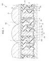
- FIG. 1 schematically illustrates a section of an optical detection device according to a first embodiment of the present disclosure.
- An optical detection device 1000 illustrated in FIG. 1 includes a plurality of unit pixel cells 10 A each including a photosensor 100 A.
- the plurality of unit pixel cells 10 A are arrayed in a matrix pattern, for example, and they form a photosensor array.
- FIG. 1 schematically illustrates respective sections of three unit pixel cells 10 A, which are arranged in a row direction of the photosensor array, among the plurality of unit pixel cells 10 A.
- FIG. 1 merely schematically illustrates the layout of individual components constituting the optical detection device 1000 , and that sizes of the components illustrated in FIG. 1 do not always exactly reflect the sizes in an actual device. Such a point is similarly applied to the other drawings in the present disclosure.
- the unit pixel cells 10 A are formed in and on a semiconductor substrate 20 .
- the semiconductor substrate 20 is, for example, a p-type silicon (Si) substrate.
- the unit pixel cells 10 A are electrically isolated from each other by element isolation regions 20 t that are formed in the semiconductor substrate 20 .
- a distance (pixel pitch) between adjacent two of the unit pixel cells 10 A may be about 2 ⁇ m, for example.
- the “semiconductor substrate” used in this specification is not limited to a substrate that is entirely a semiconductor layer, and it may be, for example, an insulating substrate including a semiconductor layer that is formed on a surface at the side irradiated with light.
- the photosensor 100 A in the unit pixel cell 10 A has a device structure substantially similar to that of a field effect transistor (FET).
- the photosensor 100 A includes impurity regions (n-type regions in this embodiment) 20 s and 20 d that are both formed in the semiconductor substrate 20 , a gate insulating layer 23 that is arranged on a region sandwiched between the impurity regions 20 s and 20 d both formed in the semiconductor substrate 20 , and a transparent gate electrode 22 g that is arranged on the gate insulating layer 23 .
- the transparent gate electrode 22 g is arranged on an interlayer insulating layer 50 covering the semiconductor substrate 20 .
- the interlayer insulating layer 50 has a multilayer structure including a plurality of insulating layers (typically, silicon oxide films).
- a multilayer wiring 40 is disposed in the interlayer insulating layer 50 .
- the multilayer wiring 40 includes a plurality of wiring layers.
- the multilayer wiring 40 includes three wiring layers.
- a power supply wiring line 42 , an address signal line 44 , and a vertical signal line 46 are disposed in middle one of the three wiring layers.
- the power supply wiring line 42 , the address signal line 44 , and the vertical signal line 46 extend, for example, along a direction perpendicular to the drawing sheet (i.e., in a column direction in the photosensor array). In the example illustrated in FIG.
- the interlayer insulating layer 50 and the multilayer wiring 40 include four insulating layers and three wiring layers, respectively.
- the number of the insulating layers in the interlayer insulating layer 50 and the number of the wiring layers in the multilayer wiring 40 are not limited to the above-mentioned examples.
- the power supply wiring line 42 in the multilayer wiring 40 is connected to the impurity region 20 d through a contact plug 52 .
- a power supply for supplying a predetermined voltage is connected to the power supply wiring line 42 .
- a predetermined bias voltage (first bias voltage) is applied to the impurity region 20 d through the power supply wiring line 42 .
- the gate insulating layer 23 penetrates through the interlayer insulating layer 50 and interconnects an upper surface of the semiconductor substrate 20 and a lower surface of the transparent gate electrode 22 g . It is to be noted that the words “upper surface” and “lower surface” in this specification are used to represent a relative positional relation in arrangement of members and are not intended to limit a posture of the optical detection device according to the present disclosure.
- the gate insulating layer 23 includes a photoelectric conversion layer 23 p .
- a thickness of the photoelectric conversion layer 23 p (i.e., a length measured along a normal direction of the semiconductor substrate 20 ) is about 1500 nm, for example. Details of a typical example of configuration of the photoelectric conversion layer 23 p will be described later.
- an insulating layer 23 x is disposed between the photoelectric conversion layer 23 p and the semiconductor substrate 20 .
- the insulating layer 23 x may be in contact with the semiconductor substrate 20 .
- the transparent gate electrode 22 g on the interlayer insulating layer 50 is formed to extend over the plurality of unit pixel cells 10 A.
- the transparent gate electrode 22 g is connected to the power supply (not illustrated).
- the transparent gate electrode 22 g is constituted such that, during the operation of the optical detection device 1000 , a predetermined bias voltage (second bias voltage) can be applied to the transparent gate electrode 22 g.
- the transparent gate electrode 22 g may be formed in a state separated for each of the unit pixel cells 10 A.
- the light is applied to the optical detection device 1000 from one side of the photosensor 100 A, the side including the transparent gate electrode 22 g , (i.e., from the upper side in FIG. 1 ) in the state where the potential difference between the transparent gate electrode 22 g and the impurity region 20 d is maintained constant.
- the light applied to the optical detection device 1000 enters the photoelectric conversion layer 23 p of the gate insulating layer 23 through the transparent gate electrode 22 g .
- the photoelectric conversion layer 23 p Upon irradiation with the incident light, the photoelectric conversion layer 23 p generates electron-hole pairs.
- the dielectric constant of the photoelectric conversion layer 23 p is changed with the generation of electron-hole pairs in the photoelectric conversion layer 23 p .
- a change of the dielectric constant of the photoelectric conversion layer 23 p provides a similar effect to that obtained when a gate capacitance of the field effect transistor is changed.
- the magnitude of a current flowing between the impurity regions 20 s and 20 d is changed with the light irradiation of the gate insulating layer 23 .
- the light can be detected by utilizing the change of the current.
- the photosensor 100 A may be called a capacitance-modulated transistor.
- the impurity regions 20 s and 20 d correspond to, for example, a source region and a drain region of the capacitance-modulated transistor, respectively.
- the impurity region 20 s is called a source region (or a drain region) of the photosensor
- the impurity region 20 d is called a drain region (or a source region) of the photosensor in some cases.
- a current flowing between the impurity regions 20 s and 20 d is simply called a drain current for the sake of simplicity in some cases.
- FIG. 1 illustrates the configuration of the optical detection device 1000 when the optical detection device 1000 is utilized as an infrared detection device.
- the light detected by the optical detection device 1000 is not limited to light within the wavelength range of visible light (e.g., 380 nm or more to 780 nm or less).
- overall electromagnetic waves including infrared rays and ultraviolet rays are expressed by “light” for the sake of convenience.
- transparent used in this specification stands for the property of allowing transmission of at least part of light in a wavelength range to be detected, and it is not essential to allow transmission of light in the entire wavelength range of visible light.
- a transparent conducting oxide (TCO) having a high transmittance for near infrared rays and a small resistance value is used as a material of the transparent gate electrode 22 g .
- TCO transparent conducting oxide
- ITO, IZO, AZO, FTO, SnO 2 , TiO 2 , or ZnO 2 can be used as TCO.
- a metal thin film made of Au, for example, may be used as the transparent gate electrode 22 g .
- a microlens 28 for condensing the irradiation light to be incident upon the photoelectric conversion layer 23 p may be arranged on the infrared transmission filter 26 .
- a protective layer may be arranged between the microlens 28 and the transparent gate electrode 22 g.
- each unit pixel cell 10 A includes an address transistor 30 .
- the address transistor 30 includes the impurity region 20 s and an impurity region 30 s both formed in the semiconductor substrate 20 , a gate insulating layer 33 , and a gate electrode 34 .
- the gate insulating layer 33 is, for example, a thermal oxide film of silicon (i.e., a silicon dioxide film).
- the gate electrode 34 is, for example, a polysilicon electrode.
- the address transistor 30 and the photosensor 100 A share the impurity region 20 s . By sharing the impurity region 20 s , the address transistor 30 and the photosensor 100 A are electrically connected to each other.
- the impurity region 20 s in the address transistor 30 functions, for example, as a drain region of the address transistor 30 .
- the impurity region 30 s in the address transistor 30 functions, for example, as a source region of the address transistor 30 .
- the gate electrode 34 (typically a polysilicon electrode) of the address transistor 30 is connected to the address signal line 44 of the multilayer wiring 40 through the contact plug 52 .
- the impurity region 30 s of the address transistor 30 is connected to the vertical signal line 46 of the multilayer wiring 40 through the contact plug 52 . Accordingly, a signal generated by the photosensor 100 A can be selectively read out through the vertical signal line 46 by controlling a potential of the gate electrode 34 through the address signal line 44 so as to turn on the address transistor 30 .
- the above-mentioned multilayer wiring 40 including the vertical signal line 46 , etc. as part thereof is formed of a metal such as copper, for example.
- a light-shielding film may be formed by one wiring layer in the multilayer wiring 40 .
- the light (infrared rays in this embodiment) having not entered the photoelectric conversion layer 23 p can be suppressed from entering a channel region of a transistor (e.g., the capacitance-modulated transistor or the address transistor 30 ) that is formed in and on the semiconductor substrate 20 .
- the insulating layer 23 x and/or the gate insulating layer 33 may have a light-shielding property. By suppressing incidence of stray light upon the channel region, it is possible to suppress mixing of noise, such as color mixing between the unit pixel cells adjacent to each other.
- most part going toward the photoelectric conversion layer 23 p is absorbed by the photoelectric conversion layer 23 p . Therefore, the light going toward the photoelectric conversion layer 23 p does not adversely affect the operation of the transistor formed in and on the semiconductor substrate 20 .
- FIG. 2 illustrates an exemplary circuit configuration of the optical detection device 1000 .
- the photosensor 100 A has a similar device structure to that of a field effect transistor. For that reason, the photosensor 100 A is conveniently expressed here using similar circuit symbols to those used for a transistor.
- FIG. 2 schematically illustrates an example in which the unit pixel cells 10 A are arrayed in a matrix pattern of two rows and two columns.
- directions in which a row and a column extend are called respectively a row direction and a column direction in some cases.
- the number and the layout of the unit pixel cells in the optical detection device 1000 are not limited to those illustrated in the example of FIG. 2 .
- the unit pixel cells may be arrayed one-dimensionally. In such a case, the optical detection device 1000 serves as a line sensor.
- the number of the unit pixel cells included in the optical detection device 1000 may be two or more, or may be one.
- the impurity region 20 d (which may be called the drain of the capacitance-modulated transistor) in the photosensor 100 A of each unit pixel cell 10 A is connected to the power supply wiring line 42 .
- the power supply wiring lines 42 are arranged in a one-to-one relation to the columns of the photosensor array. Those power supply wiring lines 42 are connected to a voltage supply circuit 12 .
- the voltage supply circuit 12 supplies the predetermined voltage (first bias voltage) to each of the unit pixel cells 10 A, which constitute the photosensor array, through the power supply wiring line 42 .
- the transparent gate electrode 22 g in the photosensor 100 A of each unit pixel cell 10 A is connected to a gate voltage control line 48 .
- the gate voltage control line 48 is connected to the voltage supply circuit 12 .
- the predetermined gate voltage (second bias voltage) is applied to the transparent gate electrode 22 g of each photosensor 100 A in the photosensor array from the voltage supply circuit 12 through the gate voltage control line 48 .
- the voltage supply circuit 12 is not limited to a particular power supply circuit, and it may be a circuit for generating a predetermined voltage, or a circuit for converting a voltage supplied from another power supply to a predetermined voltage.
- the gate voltage within a predetermined range with a potential in the impurity region 20 d of the photosensor 100 A being a reference is applied to the transparent gate electrode 22 g of each photosensor 100 A.
- the address signal line 44 connected to the gate of the address transistor 30 is connected to a vertical scanning circuit (also called a “row scanning circuit”) 14 .
- the vertical scanning circuit 14 applies a predetermined voltage to the address signal line 44 , thereby selecting the plurality of unit pixel cells 10 A, which are arranged in each row, in units of row.
- signals of the selected unit pixel cells 10 A can be read out through the address transistor 30 .
- one (typically the drain) of the source and the drain of the address transistor 30 is connected to the impurity region 20 s (which may also be called the source of the capacitance-modulated transistor) in the photosensor 100 A, and the other (the source in this embodiment) of the source and the drain of the address transistor 30 is connected to the vertical signal line 46 that is disposed for each column of the photosensor array.
- the vertical signal line 46 is a main signal line through which pixel signals are transmitted from the photosensor array to a peripheral circuit.
- a constant-current source 49 is connected between the vertical signal line 46 and a ground. Accordingly, a change of the drain current in the photosensor 100 A, the change being attributable to the light irradiation of the photosensor 100 A, can be detected by detecting a voltage change in the vertical signal line 46 . Stated in another way, the light can be detected in accordance with the voltage change in the vertical signal line 46 .
- the power supply wiring line 42 functions as a source follower power supply. The light may be detected by detecting a current that is output from the impurity region 20 s of the photosensor 100 A. However, it is more advantageous to detect the voltage change from the viewpoint that a similar process and circuit to those utilized for a photosensor using a silicon photodiode can be applied, and that a higher S/N ratio can be obtained.
- a circuit for supplying the predetermined voltage to the impurity region 20 d in the photosensor 100 A and a circuit for supplying the predetermined voltage to the transparent gate electrode 22 g may be one common circuit as illustrated in FIG. 2 , or may be different from each other. At least one of the circuit for supplying the predetermined voltage to the impurity region 20 d in the photosensor 100 A and the circuit for supplying the predetermined voltage to the transparent gate electrode 22 g may be part of the vertical scanning circuit 14 .
- a semiconductor material is typically used to constitute the photoelectric conversion layer 23 p .
- the photoelectric conversion layer 23 p Upon receiving the irradiation light, the photoelectric conversion layer 23 p generates electron-hole pairs therein.
- an organic semiconductor material is used to constitute the photoelectric conversion layer 23 p .
- the photoelectric conversion layer 23 p contains, for example, tin naphthalocyanine expressed by the following general formula (1) (hereinafter simply called “tin naphthalocyanine” in some cases).
- R 1 to R 24 denote hydrogen atoms or substituents independently of one another.
- the substituents are not limited to particular ones.
- the substituents may be a deuterium atom, a halogen atom, alkyl groups (including a cycloalkyl group, a bicycloalkyl group, and a tricycloalkyl group), alkenyl groups (including a cycloalkenyl group and a bicycloalkenyl group), an alkynyl group, an aryl group, a heterocyclic group (also called a heterocyclic ring group), a cyano group, a hydroxy group, a nitro group, a carboxy group, an alkoxy group, an aryloxy group, a silyloxy group, a heterocyclic oxy group, an acyloxy group, a carbamoyloxy group, an alkoxycarbonyloxy group, an aryloxy carbonyloxy group, amino groups (including
- the tin naphthalocyanine expressed by the above general formula (1) may be a commercially available product.
- the tin naphthalocyanine expressed by the above general formula (1) can be synthesized using, as a starting material, a naphthalene derivative that is expressed by the following general formula (2), as set forth in Japanese Unexamined Patent Application Publication No. 2010-232410, for example.
- R 25 to R 30 in the general formula (2) may be substituents similar to those used as R 1 to R 24 in the general formula (1).
- tin naphthalocyanine expressed by the above general formula (1) it is desirable, from the viewpoint of easiness in control of a molecular aggregation state, that eight or more among R 1 to R 24 are hydrogen atoms or deuterium atoms. More desirably, sixteen or more among R 1 to R 24 are hydrogen atoms or deuterium atoms. Even more desirably, all of R 1 to R 24 are hydrogen atoms or deuterium atoms. Additionally, tin naphthalocyanine expressed by the following general formula (3) is advantageous from the viewpoint of easiness in synthesis.
- the tin naphthalocyanine expressed by the above general formula (1) exhibits absorption in a wavelength band of about 200 nm or more and about 1100 nm or less.
- the tin naphthalocyanine expressed by the above general formula (3) for example, has an absorption peak at the wavelength of about 870 nm as depicted in FIG. 3 .
- FIG. 3 depicts one example of an absorption spectrum of a photoelectric conversion layer containing the tin naphthalocyanine expressed by the above general formula (3).
- a sample including the photoelectric conversion layer (thickness: 30 nm) laminated on a quartz substrate is used in measurement of the absorption spectrum.
- the photoelectric conversion layer formed of a material containing the tin naphthalocyanine exhibits absorption in a near-infrared region.
- an optical sensor capable of detecting near-infrared rays can be realized by selecting, as a material constituting the photoelectric conversion layer 23 p , a material containing the tin naphthalocyanine.
- FIG. 4 illustrates one example of the gate insulating layer including the photoelectric conversion layer that is formed using an organic semiconductor layer containing the tin naphthalocyanine expressed by the above general formula (1).
- the gate insulating layer 23 includes a photoelectric conversion structure 230 A.
- the gate insulating layer 23 further includes an electron blocking layer 234 that is disposed between the photoelectric conversion structure 230 A and the transparent gate electrode 22 g , and a hole blocking layer 236 that is disposed between the photoelectric conversion structure 230 A and the insulating layer 23 x.
- the photoelectric conversion structure 230 A includes at least one of a p-type semiconductor and an n-type semiconductor.
- the photoelectric conversion structure 230 A includes a p-type semiconductor layer 230 p , an n-type semiconductor layer 230 n , and a photoelectric conversion layer 230 h sandwiched between the p-type semiconductor layer 230 p and the n-type semiconductor layer 230 n .
- the p-type semiconductor layer 230 p is disposed between the electron blocking layer 234 and the photoelectric conversion layer 230 h , and it has the functions of a photoelectric conversion layer and/or a hole transport layer.
- the n-type semiconductor layer 230 n is disposed between the hole blocking layer 236 and the photoelectric conversion layer 230 h , and it has the functions of a photoelectric conversion and/or an electron transport layer.
- the photoelectric conversion layer 230 h may include at least one of a p-type semiconductor and an n-type semiconductor.
- the p-type semiconductor layer 230 p includes an organic p-type semiconductor
- the n-type semiconductor layer 230 n includes an organic n-type semiconductor.
- the photoelectric conversion structure 230 A includes an organic photoelectric conversion material containing the tin naphthalocyanine expressed by the above general formula (1), and at least one of an organic p-type semiconductor and an organic n-type semiconductor.
- the organic p-type semiconductor implies a donor organic semiconductor (compound), i.e., an organic compound that has electron-donating properties, and that is mainly represented by a hole transport organic compound. More specifically, when two organic materials are used in a contact state, one of those two organic compounds, which exhibits a smaller ionization potential, is called the organic p-type semiconductor (compound). Thus, any type of organic compound can be used as the donor organic compound insofar as it is an organic compound with electron-donating properties.
- Examples of that type of organic compound include a triarylamine compound, a benzidine compound, a pyrazoline compound, a styryl amine compound, a hydrazone compound, a triphenylmethane compound, a carbazole compound, a polysilane compound, a thiophene compound, a phthalocyanine compound, a cyanine compound, a merocyanine compound, an oxonol compound, a polyamine compound, an indole compound, a pyrrole compound, a pyrazole compound, a polyarylene compound, condensed aromatic carboncyclic compounds (such as a naphthalene derivative, an anthracene derivative, a phenanthrene derivative, a tetracene derivative, a pyrene derivative, a perylene derivative, and a fluoranthene derivative), and a metal complex having a nitrogen-containing heterocyclic compound as a ligand.
- the donor organic semiconductor is not limited to the above-mentioned examples.
- the donor organic semiconductor may be any type of organic compound having a smaller ionization potential than an organic compound that is used as the n-type (acceptor) compound.
- the above-mentioned tin naphthalocyanine is one example of the organic p-type semiconductor material.
- the organic n-type semiconductor implies an acceptor organic semiconductor (compound), i.e., an organic compound that has electron-accepting properties, and that is mainly represented by an electron transport organic compound. More specifically, when two organic materials are used in a contact state, one of those two organic compounds, which exhibits a larger electron affinity, is called the organic n-type semiconductor (compound). Thus, any type of organic compound can be used as the acceptor organic compound insofar as it is an organic compound with electron-accepting properties.
- Examples of that type of organic compound include fullerene, a fullerene derivative, condensed aromatic carboncyclic compounds (such as a naphthalene derivative, an anthracene derivative, a phenanthrene derivative, a tetracene derivative, a pyrene derivative, a perylene derivative, and a fluoranthene derivative), five- to seven-membered heterocyclic compounds containing a nitrogen atom, an oxygen atom, and a sulfur atom (such as pyridine, pyradine, pyrimidine, pyridazine, triazine, quinoline; quinoxaline; quinazoline, phthalazine, cinnoline, isoquinoline, pteridine, acridine, phenazine, phenanthroline, tetrazole, pyrazole, imidazole, thiazole, oxazole, indazole, benzimidazole, benzotri
- the photoelectric conversion layer 230 h may be; for example, a bulk heterojunction structure layer including a p-type semiconductor and an n-type semiconductor.
- the photoelectric conversion layer 230 h is formed as a layer having the bulk heterojunction structure, the tin naphthalocyanine expressed by the above general formula (1) can be used as the p-type semiconductor material.
- Fullerene and/or a fullerene derivative, for example, can be used as the n-type semiconductor material. It is desirable that the material constituting the p-type semiconductor layer 230 p is the same as the p-type semiconductor material contained in the photoelectric conversion layer 230 h .
- the material constituting the n-type semiconductor layer 230 n is the same as the n-type semiconductor material contained in the photoelectric conversion layer 230 h .
- the bulk heterojunction structure is described in detail in Japanese Patent No. 5553727. For reference, the entire contents of Japanese Patent No. 5553727 are assumed to be incorporated in this specification.
- a photosensor having sensitivity in a desired wavelength range can be realized by employing a proper material depending on the wavelength range to be detected.
- the photoelectric conversion layer 23 p may include an inorganic semiconductor material, such as amorphous silicon.
- the photoelectric conversion layer 23 p may include a layer made of an organic material and a layer made of an inorganic material. The following description is made in connection with an example in which the bulk heterojunction structure obtained by co-evaporation of the tin naphthalocyanine and C 50 is employed in the photoelectric conversion layer 23 p.
- FIG. 5 depicts a typical example of photocurrent characteristics in the photoelectric conversion layer 23 p .
- a graph denoted by a thick solid line represents, by way of example, current-voltage characteristics (I-V characteristics) of the photoelectric conversion layer 23 p in a state where the photoelectric conversion layer is irradiated with light.
- I-V characteristics current-voltage characteristics
- FIG. 5 depicts changes of a current density between two principal surfaces of the photoelectric conversion layer when a bias voltage applied to those two principal surfaces is changed under constant illuminance.
- a forward direction and a reverse direction of the bias voltage are defined as follows.
- a bias voltage providing a higher potential in the layer of the p-type semiconductor than in the layer of the n-type semiconductor is defined as the bias voltage in the forward direction.
- a bias voltage providing a lower potential in the layer of the p-type semiconductor than in the layer of the n-type semiconductor is defined as the bias voltage in the reverse direction.
- the forward direction and the reverse direction can be defined as in the case of employing inorganic semiconductor materials.
- a bias voltage providing a potential on the side near the principal surface where the p-type semiconductor appears at a larger proportion than the n-type semiconductor, the potential being higher than that on the side near the principal surface where the n-type semiconductor appears at a larger proportion than the p-type semiconductor, is defined as the bias voltage in the forward direction.
- the photocurrent characteristics in the photoelectric conversion layer according to the embodiment of the present disclosure are roughly featured by three, i.e., first to third, voltage ranges.
- the first voltage range represents a reverse-bias voltage range where an absolute value of an output current density increases as the bias voltage in the reverse direction increases.
- the first voltage range may be called a voltage range where a photocurrent increases as the bias voltage applied between the principal surfaces of the photoelectric conversion layer increases.
- the second voltage range represents a forward-bias voltage range where the output current density increases as the bias voltage in the forward direction increases.
- the second voltage range is a voltage range where a current in the forward direction increases as the bias voltage applied between the principal surfaces of the photoelectric conversion layer increases.
- the third voltage range is a voltage range between the first voltage range and the second voltage range.
- the first to third voltage ranges can be discriminated in accordance with a gradient of the graph representing the photocurrent characteristics when the vertical axis and the horizontal axis are each expressed in a linear scale.
- a gradient of the graph in the first voltage range is denoted by a dotted line L 1
- an average gradient of the graph in the second voltage range is denoted by a dotted line L 2 .
- a rate of change of the output current density relative to an increase of the bias voltage is different among the first voltage range, the second voltage range, and the third voltage range.
- the third voltage range is defined as a voltage range where the rate of change of the absolute value of the output current density relative to the bias voltage is smaller than the rate of change in the first voltage range and the rate of change in the second voltage range.
- the third voltage range may be determined on the basis of a position of rising (falling) in the graph that represents the I-V characteristics.
- the third voltage range is entirely larger than ⁇ 1 V and entirely smaller than +1 V.
- the absolute value of the current density in the third voltage range is typically not more than 100 ⁇ A/cm 2 .
- the hole-electron pairs generated with the light irradiation promptly recombine and disappear upon stop of the light irradiation. Therefore, a high-speed response can be realized by adjusting the bias voltage, which is applied between the two principal surfaces of the photoelectric conversion layer during the operation of the optical detection device, to the voltage within the third voltage range.
- the detection of the light is performed in a state where a potential difference between one of the two impurity regions of the photosensor, the one being connected to the power supply wiring line 42 , and the transparent gate electrode 22 g is maintained within the above-mentioned third voltage range during the operation of the optical detection device.
- the gate voltage with the impurity region 20 d being a reference falling within the third voltage range is supplied to the transparent gate electrode 22 g from the voltage supply circuit 12 .
- the photoelectric conversion layer 23 p is in a state where the bias voltage within the third voltage range is applied between its upper surface (i.e., a principal surface on the side close to the transparent gate electrode 22 g ) and its lower surface.
- E denotes the magnitude of an electric field within the photoelectric conversion layer 23 p in a state applied with the predetermined bias voltage and is irradiated with the light
- E (( ⁇ f ⁇ p )/ ⁇ 0 )
- ⁇ f denotes a charge density in an electrode (e.g., the transparent gate electrode 22 g )
- ⁇ p denotes a density of charges generated due to polarization in a surface of the photoelectric conversion layer 23 p , the surface being opposed to the electrode.
- c and E denote respectively the dielectric constant of vacuum and the dielectric constant of the photoelectric conversion layer 23 p .
- the photosensor 100 A Assuming here the photosensor 100 A to be a transistor, with an increase of the dielectric constant of the gate insulating layer 23 , a threshold voltage is reduced (this can also be said that an effective gate voltage is increased). Thus, the magnitude of a drain current flowing between the impurity regions 20 d and 20 s is changed due to a change of the dielectric constant of the gate insulating layer 23 . Stated in another way, the magnitude of the drain current in the photosensor 100 A is changed depending on a change of the illuminance applied to the photosensor 100 A. Accordingly, the light can be detected by detecting the change of the magnitude of the drain current with an appropriate detection circuit.
- the change of the threshold voltage depending on the change of the illuminance applied to the photosensor 100 A can be detected as a voltage change in the vertical signal line 46 .
- a constant-voltage source may be connected to the vertical signal line 46 , and a current change in the vertical signal line 46 may be detected.
- an output signal from the photosensor 100 A may be given as a voltage change or a current change.
- the bias voltage within the third voltage range is applied to the photoelectric conversion layer 23 p during the detection of the light.
- an operation of detecting light is generally performed under application of a reverse bias, which corresponds to the first voltage range illustrated in FIG. 5 . Therefore, holes and electrons generated with the photoelectric conversion drift respectively toward a cathode and an anode of the photodiode.
- charges generated with the photoelectric conversion are taken out as a signal to an external circuit.
- the bias voltage within the third voltage range is applied to the photoelectric conversion layer 23 p during the detection of the light.
- the photoelectric conversion layer 23 p is irradiated with the light in the state where the bias voltage within the third voltage range is applied, hole-electron pairs are generated in the photoelectric conversion layer 23 p .
- the generated holes and electrons form dipoles without separating from each other and drifting to the electrodes. In other words, the generated holes and electrons are not taken out to the outside of the photoelectric conversion layer 23 p.
- Respective speeds of outflow of charges from the photoelectric conversion layer and inflow of charges into the photoelectric conversion layer are slow (about several tens milliseconds). Accordingly, when the photosensor is applied to an image sensor, the configuration accompanying with the outflow of charges from the photoelectric conversion layer or the inflow of charges into the photoelectric conversion layer gives rise to a possibility of causing noise, a residual image, etc. with application of the voltage to the photoelectric conversion layer and the light irradiation at the start of image-taking, etc. On the other hand, with the configuration of setting the bias voltage applied to the photoelectric conversion layer 23 p to the voltage within the third voltage range during the detection of the light, the occurrence of noise, a residual image, etc. can be suppressed because of not accompanying with the outflow of charges from the photoelectric conversion layer or the inflow of charges into the photoelectric conversion layer.
- the photosensor according to the embodiment of the present disclosure can be advantageously applied to range sensing with the time-of-flight method, ultra-high-speed image taking, etc.
- the first bias voltage applied to the impurity region 20 d through the power supply wiring line 42 is 2.4 V, for example, and the second voltage applied to the transparent gate electrode 22 g through the gate voltage control line 48 is 2.5 V, for example.
- a potential difference of about 0.1 V is applied between the upper and lower surfaces of the gate insulating layer 23 in the photosensor 100 A.
- the detection of the light can also be performed by applying the bias voltage within the first voltage range to the photoelectric conversion layer.
- a photoelectric conversion material exhibiting absorption in an infrared region has a narrow bandgap. Activation energy in a current attributable to thermal excitation, the current causing a dark current, is proportional to the bandgap. Accordingly, when the photoelectric conversion material exhibiting absorption in the infrared region is used as a material of the gate insulating layer of the capacitance-modulated transistor, there is a possibility that a sufficient S/N ratio cannot be ensured with generation of a gate leak.
- the magnitude of a leak current in an organic photoelectric conversion layer alone under application of a bias voltage may be 0.1 V is, for example, about 1 ⁇ 10 ⁇ 8 A/cm 2 (where “x” denotes multiplication).
- a photoelectric conversion layer exhibiting absorption in a near infrared region is used as the photoelectric conversion layer 23 p .
- the insulating layer 23 x is disposed between the photoelectric conversion layer 23 p and the semiconductor substrate 20 .
- a thermal oxide film of silicon for example, may be used as the insulating layer 23 x .
- FIG. 6 depicts dependency, on a film thickness, of a leak current that flows in the thermal oxide film of silicon when a voltage of 0.1 V is applied.
- the leak current in the gate insulating layer 23 is not more than 1 ⁇ 10 ⁇ 11 A/cm 2 .
- the magnitude of the leak current at such a level corresponds to a leak amount of not more than 1 e/s on an assumption that an area (gate area) when looking at the gate insulating layer 23 from the normal direction of the semiconductor substrate 20 is 1 ⁇ m 2 (“e” as a unit of the leak amount denotes the number of electrons).
- e as a unit of the leak amount denotes the number of electrons.
- the voltage applied between the upper surface and the lower surface of the photoelectric conversion layer 23 p during the detection of the light is relatively small, namely about 0.1 V, for example. Therefore, it is relatively easy to use a material having a narrow bandgap as the material of the photoelectric conversion layer 23 p . Furthermore, the leak current to the channel region of the capacitance-modulated transistor can be reduced with the provision of the insulating layer 23 x between the photoelectric conversion layer 23 p and the semiconductor substrate 20 .
- the potential difference applied between the impurity region 20 d and the transparent gate electrode 22 g is relatively small. Accordingly, an insulating film being relatively thin can be used as the insulating layer 23 x , and information regarding the illuminance can be obtained, for example, in terms of modulation of the drain current.
- the material constituting the insulating layer 23 x is not limited to silicon dioxide.
- a silicon oxynitride film (SiON film), which is generally used in silicon semiconductors, may be used as the insulating layer 23 x .
- a High-k film, such as a HfO 2 film, may also be used.
- the thickness of the insulating layer 23 x may be set as appropriate depending on the material that is used to constitute the insulating layer 23 x.
- Imaging with use of near infrared rays has promise in the fields of, for example, a night vision system loaded on a vehicle and vital observation, and a photosensor having sensitivity in the infrared region is demanded.
- the band gap of silicon is 1.1 eV, and a photosensor using a silicon photodiode cannot detect light with a wavelength of 1100 nm or longer.
- the silicon photodiode has sensitivity in the wavelength range of about 900 nm, the sensitivity is lower than that in the wavelength range of visible light, and an improvement of performance is demanded particularly in applications to the night vision system.
- In x Ga 1-x As is known as a semiconductor having a narrow bandgap.
- the bandgap of In x Ga 1-x As can be narrowed to 0.3 eV by adjusting a composition ratio X.
- a photosensor using In x Ga 1-x As can be given with sensitivity for a wavelength of 3 ⁇ m at maximum, and hence the photosensor using In x Ga 1-x As can be employed as an infrared sensor.
- an image sensor needs to be cooled in order to suppress degradation of an S/N ratio, which is caused by the dark current attributable to crystal defects and by thermal noise attributable to the narrow bandgap. Accordingly, that type of sensor has a difficulty in reducing the size and the cost, and it has not yet been widely employed for consumer use.
- a microbolometer and a pyroelectric sensor are known as infrared image sensors not using cooling devices.
- the microbolometer and the pyroelectric sensor perform detection of infrared rays based on heat, a response speed is as slow as several ten milliseconds, and applications of those sensors are restricted.
- the photoelectric conversion layer 23 p the material exhibiting absorption in the infrared region.
- the photoelectric conversion layer containing the tin naphthalocyanine expressed by the above-mentioned formula (3) has an absorption peak in the wavelength range of 80 nm to 1000 nm, as depicted in FIG. 3 .
- the quantum efficiency of the photoelectric conversion layer containing the tin naphthalocyanine expressed by the formula (3) at the wavelength of 900 nm may be about ten times that of silicon.
- a photosensor having sensitivity in the infrared region can be realized with a comparatively simple configuration. Since the detection performed by the photosensor according to the embodiment of the present disclosure is not based on heat, generation of thermal noise attributable to temperature change in a channel portion can be avoided, and there is no need of providing a cooling mechanism.
- the optical detection device 1000 can be manufactured by employing general semiconductor manufacturing processes.
- the optical detection device 1000 can be manufactured by utilizing various silicon semiconductor processes. Since the photosensor according to the present disclosure has a similar device structure to that of a field effect transistor, it is also relatively easy to form other transistors and the photosensor according to the present disclosure on the same semiconductor substrate.
- FIG. 7 schematically illustrates a section of an optical detection device according to a second embodiment of the present disclosure.
- an optical detection device 1000 includes a plurality of unit pixel cells 10 B each including a photosensor 100 B.
- FIG. 7 for the sake of avoiding the drawing from being complicated, only one of the unit pixel cells 10 B is illustrated.
- the photosensor 100 B includes a capacitance-modulated transistor 60 and a photoelectric conversion portion.
- the capacitance-modulated transistor 60 is a field effect transistor formed in and on the semiconductor substrate 20 .
- the capacitance-modulated transistor 60 includes an impurity region 20 d , an impurity region 20 s , an insulating layer 23 x on the semiconductor substrate, and a gate electrode 24 on the insulating layer 23 x .
- the impurity region 20 d functions as a drain region (or a source region) of the capacitance-modulated transistor 60
- the impurity region 20 s functions as the source region (or the drain region) of the capacitance-modulated transistor 60 .
- the impurity region 20 d is connected to the power supply wiring line 42 such that the predetermined voltage (first bias voltage) can be applied to the impurity region 20 d during the operation of the optical detection device 1000 .
- the insulating layer 23 x serves as a gate insulating layer of the capacitance-modulated transistor 60 .
- the insulating layer 23 x is a thermal oxide film of silicon with a thickness of 4.6 nm, for example.
- the photoelectric conversion portion of the photosensor 100 B includes a pixel electrode 21 , a transparent electrode 22 opposing to the pixel electrode 21 , and a photoelectric conversion layer 23 p sandwiched between the pixel electrode 21 and the transparent electrode 22 .
- the pixel electrode 21 is spatially separated from other adjacent pixel cells 10 B, whereby it is electrically isolated from the pixel electrodes 21 of the other pixel cells 10 B.
- the pixel electrode 21 is typically a metal electrode or a metal nitride electrode. Examples of materials usable to form the pixel electrode 21 are Al, Cu, Ti, TiN, Ta, TaN, Mo, Ru, and Pt.
- the pixel electrode 21 may be formed of, for example, polysilicon that is doped with impurities to be given with conductivity. In this embodiment, a TiN electrode is used as the pixel electrode 21 .
- the photoelectric conversion layer 23 p is formed to extend up to regions of the other unit pixel cells 10 B.
- the photoelectric conversion layer 23 p may have a thickness of about 200 nm, for example.
- the transparent electrode 22 is also formed to extend up to regions of the other unit pixel cells 10 B by employing a TCO.
- the transparent electrode 22 is connected to the gate voltage control line 48 (not illustrated in FIG. 7 , see FIG. 2 ) such that the predetermined voltage (second bias voltage) can be applied to the transparent electrode 22 during the operation of the optical detection device 1000 .
- the transparent electrode 22 and the photoelectric conversion layer 23 p are arranged on the interlayer insulating layer 50 .
- the pixel electrode 21 of the photoelectric conversion portion and the gate electrode 24 of the capacitance-modulated transistor 60 are connected to each other by a connection portion 54 , which includes part of the multilayer wiring 40 and a contact plug 52 .
- the photosensor 100 B according to the second embodiment has a structure in which an electrode (constituted by the pixel electrode 21 , the connection portion 54 , and the gate electrode 24 in the illustrated example) is interposed between the photoelectric conversion layer 23 p and the insulating layer 23 x in the photosensor 100 A (see FIG. 1 ) according to the first embodiment.
- the capacitance-modulated transistor 60 can be regarded as including a gate insulating layer that includes serial connection of a capacitor having the insulating layer 23 x as a dielectric layer and a capacitor having the photoelectric conversion layer 23 p as a dielectric layer.
- a multilayer structure including the pixel electrode 21 , the connection portion 54 , and the gate electrode 24 between the insulating layer 23 x and the photoelectric conversion layer 23 p constitutes a gate capacitance (which may also be called a gate insulating layer) in the capacitance-modulated transistor 60
- the transparent electrode 22 constitutes a gate electrode in the capacitance-modulated transistor 60 .
- the principle of light detection in the optical detection device 1000 according to the second embodiment is substantially the same as that in the first embodiment. More specifically, in a state where a bias voltage within the above-described third voltage range is applied to the photoelectric conversion layer 23 p , light is incident upon the photoelectric conversion layer 23 p through the transparent electrode 22 .
- the voltage applied to the impurity region 20 d is 2.4 V, for example.
- the voltage applied to the transparent electrode 22 is 2.5 V, for example.
- a resultant bias voltage of about 0.1 V is applied between the insulating layer 23 x , which serves as the gate insulating layer of the capacitance-modulated transistor 60 , and the photoelectric conversion layer 23 p.
- an aperture ratio in the unit pixel cell 10 B is given by a ratio of a region where the pixel electrode 21 and the transparent electrode 22 overlap with each other to the unit pixel cell 10 B when the unit pixel cell 10 B is viewed from the normal direction of the semiconductor substrate 20 . Therefore, a larger aperture ratio can be more easily obtained than in the case of employing the structure (see FIG. 1 ) in which the photoelectric conversion layer 23 p is buried in the interlayer insulating layer 50 .
- the layout of the photoelectric conversion layer 23 p being arranged on the interlayer insulating layer 50 has less difficulty in a manufacturing process than the layout of the photoelectric conversion layer 23 p being buried in the interlayer insulating layer 50 , and the former layout is more advantageous from the viewpoint of manufacturing.
- the gate electrode 24 of the capacitance-modulated transistor 60 and the gate electrode 34 of the address transistor 30 are both polysilicon electrodes, the gate of the address transistor 30 can be formed at the same time as forming the gate of the capacitance-modulated transistor 60 .
- the gate electrode 24 of the capacitance-modulated transistor 60 and the gate electrode 34 of the address transistor 30 are formed using different materials, those gate electrodes need to be formed successively.
- the gate electrode 24 and the gate electrode 34 and injecting impurities with the lithography technique it is generally difficult to avoid a deviation in alignment between the gate electrode 24 and the gate electrode 34 .
- a margin needs to be set for ensuring the alignment. In other words, using different materials is disadvantageous from the viewpoint of reducing the size of the unit pixel cell in the optical detection device.
- both the gate electrodes can be formed together at desired positions and in desired shapes by employing a common mask and a common material without taking into account a deviation in the alignment.
- both the insulating layers can be formed together at desired positions and in desired shapes by employing a common mask and a common material without taking into account a deviation in the alignment. Accordingly, the pixels can be formed in smaller sizes.
- the manufacturing cost can be further reduced by designing a gate structure of the capacitance-modulated transistor 60 and a gate structure of the address transistor 30 in common to each other.
- the photosensor 100 A does not include an electrode corresponding to the gate electrode 24 of the capacitance-modulated transistor 60 (see FIG. 1 ).
- the insulating layer 23 x of the photosensor 100 A and the gate insulating layer 33 of the address transistor 30 can be formed by employing a common mask and a common material. This makes it possible to eliminate the necessity of alignment in the case of forming the gate insulating layer 33 after forming the insulating layer 23 x , or the necessity of alignment in the case of forming the insulating layer 23 x after forming the gate insulating layer 33 . Thus, a positional deviation between the insulating layer 23 x and the gate insulating layer 33 can be eliminated by designing the insulating layer 23 x and the gate insulating layer 33 to be positioned in the same layer.
- the pixel electrode 21 By forming the pixel electrode 21 as an electrode with a light-shielding property, stray light can be suppressed from entering the channel region of the capacitance-modulated transistor 60 and/or the channel region of the address transistor 30 .
- An optical filter such as an infrared transmission filter, may be disposed between the transparent electrode 22 and the microlens 28 .
- the device structure illustrated in FIG. 7 apparently seems like a device structure of a stacked image sensor in which a photoelectric conversion layer is disposed on a semiconductor substrate.
- a comparatively high bias voltage is applied between a pixel electrode and a transparent electrode opposing to the pixel electrode, and ones of holes and electrons both generated in the photoelectric conversion layer with light irradiation are collected as signal charges to the pixel electrode.
- the collected signal charges are temporarily accumulated in a floating diffusion within a unit pixel cell, and a signal voltage corresponding to an amount of the accumulated charges is read out at predetermined timing.
- holes and electrons generated in the photoelectric conversion layer 23 p are not drifted toward the electrodes, and an electrical signal corresponding to a change of the dielectric constant of the photoelectric conversion layer 23 p is read out. Only ones of the holes and the electrons can be utilized as signal charges in the stacked image sensor, whereas the holes and the electrons are both utilized in pairs to cause a change of the drain current in the photosensor of the present disclosure. Hence higher sensitivity can be realized.
- the potential difference applied between the upper surface and the lower surface of the photoelectric conversion layer 23 p is set to the value within the above-mentioned third voltage range, the generated pairs of holes and electrons promptly recombine when the light irradiation is stopped.
- an operation of resetting the potential of the pixel electrode is not required.
- the photosensor of the present disclosure does not perform an operation of accumulating the holes or the electrons, which are generated in the photoelectric conversion layer 23 p , as the signal charges in the floating diffusion. For that reason, the semiconductor substrate 20 does not have a charge accumulation region to accumulate the signal charges, unlike the stacked image sensor.
- the generated pairs of holes and electrons promptly recombine when the light irradiation is stopped.
- an output of the photosensor represents a variation corresponding to a change of the illuminance in the state under the light irradiation, and that the output does not depend on an integrated amount of light.
- the timing of exposure and the timing of reading out a signal can be basically made coincident with each other.
- a capacitor having one electrode electrically connected to the impurity region 20 s or 30 s (see, for example, FIG. 7 ) in the semiconductor substrate 20 may be disposed in the unit pixel cell.
- the output signal can be read out at timing different from the timing of exposure of the photosensor.
- FIG. 8 schematically illustrates a section of an optical detection device according to a third embodiment of the present disclosure.
- a photosensor 100 C in a unit pixel cell 10 C, illustrated in FIG. 8 is different from the photosensor 109 E in the second embodiment, described above with reference to FIG. 7 , in that a photoelectric conversion portion of the photosensor 100 C includes an insulating layer disposed between the photoelectric conversion layer 23 p and an electrode (i.e., one or each of a pixel electrode 21 and a transparent electrode 22 ).
- insulating layers 29 a and 29 b are disposed respectively between the pixel electrode 21 and the photoelectric conversion layer 23 p and between the photoelectric conversion layer 23 p and the transparent electrode 22 .
- a material exhibiting a smaller leak current than a material constituting the photoelectric conversion layer 23 p can be selected to constitute the insulating layers 29 a and 29 b .
- a silicon oxide film having a thickness of 5.4 nm is used as each of the insulating layers 29 a and 29 b .
- the silicon oxide film can be formed by CVD, for example.
- a larger bias voltage can be applied between the drain region (or the source region) of the capacitance-modulated transistor 60 and the transparent electrode 22 .
- a voltage of 1.2 V is applied as the first bias voltage to the impurity region 20 d
- a voltage of 3.7 V is applied as the second bias voltage to the transparent electrode 22 .
- a potential difference of about 2.5 V is applied between the impurity region 20 d and the transparent electrode 22 .
- FIG. 9 depicts dependency, on a film thickness, of a leak current that flows in a silicon oxide film when a voltage of 2.5 V is applied.
- the leak current to the channel region of the capacitance-modulated transistor 60 is not more than 1 ⁇ 10 ⁇ 11 A/cm 2 .
- the leak current in the silicon oxide film can be reduced down to 1 ⁇ 10 ⁇ 11 A/cm 2 or less by setting a thickness of the silicon oxide film to 5.4 nm or more.
- the voltage applied between the impurity region 20 d and the transparent electrode 22 is divided among the insulating layer 23 x , the insulating layer 29 a , the insulating layer 29 b , and the photoelectric conversion layer 23 p , each of which constitute a capacitor. Accordingly, a voltage actually applied to each of the insulating layer 23 x , the insulating layer 29 a , and the insulating layer 29 b is about 0.8 V. In a strict sense, therefore, it is not necessary for each of the insulating layer 29 a and the insulating layer 29 b to have a thickness of 5.4 nm. In this embodiment, the thickness of each of the insulating layer 29 a and the insulating layer 29 b is set to a value of 5.4 nm, taking into account characteristic variations of silicon oxide films that are formed by CVD.
- a larger bias voltage can be applied between the drain region (or the source region) of the capacitance-modulated transistor 60 and the transparent electrode 22 .
- the bias voltage providing a potential difference between the upper surface and the lower surface of the photoelectric conversion layer 23 p , the potential difference falling within the above-mentioned first voltage range, may be applied between the drain region (or the source region) of the capacitance-modulated transistor 60 and the transparent electrode 22 .
- the timing of exposure and the timing of reading out a signal are not always required to be coincident with each other. Since the timing of exposure and the timing of reading out a signal can be made different from each other in a comparatively easy manner, applying the bias voltage within the first voltage range to the photoelectric conversion layer 23 p is advantageous from one point of view when the photosensor is applied to an image sensor.
- the insulating layer 29 a between the photoelectric conversion layer 23 p and the pixel electrode 21 is able to function as a capacitor that accumulates ones of the holes and the electrons both generated with the photoelectric conversion. With the accumulation of charges in that capacitor, electrostatic induction occurs in the connection portion 54 , whereby an effective gate voltage in the capacitance-modulated transistor 60 is changed. Accordingly, the magnitude of a drain current in the capacitance-modulated transistor 60 is changed.
- a reset operation of resetting the charges accumulated in the insulating layer 29 a is executed, for example, by applying a voltage having a polarity reversed to that of the second bias voltage to the transparent electrode 22 .
- the charges accumulated in the insulating layer 29 a which serves as a capacitor
- the charges accumulated in the insulating layer 29 b which also serves as a capacitor, may be caused to recombine by blocking the light with a mechanical shutter, for example.
- the operation of detecting the light may be performed in the state where the bias voltage within the above-mentioned third voltage range is applied to the photoelectric conversion layer 23 p . In that case, the operation of resetting the charges is not needed.
- the insulating layers may be disposed respectively between the photoelectric conversion layer 23 p and the pixel electrode 21 and between the photoelectric conversion layer 23 p and the transparent electrode 22 .
- the insulating layer 29 a and/or the insulating layer 29 b may be used as the insulating layer 29 a and/or the insulating layer 29 b.
- the transistors in the unit pixel cell such as the capacitance-modulated transistor 60 and the address transistor 30 , are each an N-channel MOS.
- the transistors used in embodiments of the present disclosure are not limited to N-channel MOS's.
- the capacitance-modulated transistor 60 and the address transistor 30 may be each an N-channel MOS or a P-channel MOS. Additionally, it is not always required that those transistors are all N-channel MOS's or P-channel MOS's.
- a bipolar transistor can also be used as the address transistor 30 .
- the address transistor 30 may be a bipolar transistor.
- Carriers in the channel formed between the impurity region 20 d and the impurity region 20 s in the photosensor 100 A may be electrons or holes.
- FIG. 10 schematically illustrates an exemplary configuration of a camera system according to a fourth embodiment of the present disclosure.
- a camera system 300 illustrated in FIG. 10 includes a lens optical system 310 , the above-described optical detection device 1000 , a system controller 330 , and a camera signal processing unit 320 .
- the lens optical system 310 includes, for example, an autofocusing lens, a zooming lens, and a diaphragm.
- the lens optical system 310 condenses light onto an imaging surface of the optical detection device 1000 .
- a color filter may be disposed on the imaging surface of the optical detection device 1000 .
- the optical detection device 1000 may include, as peripheral circuits, a column signal processing circuit (also called a “row signal accumulation circuit”), a horizontal signal reading-out circuit (also called a “column scanning circuit”), etc.
- the system controller 330 controls the entirety of the camera system 300 .
- the system controller 330 may be implemented with a microcomputer, for example.
- the camera signal processing unit 320 functions as a signal processing circuit that processes the output signal from the optical detection device 1000 .
- the camera signal processing unit 320 executes processes such as gamma correction, a color interpolation process, a spatial interpolation process, and auto white balance.
- the camera signal processing unit 320 may be implemented with a digital signal processor (DSP), for example.
- DSP digital signal processor
- At least one of the system controller 330 and the camera signal processing unit 320 may be formed on the semiconductor substrate 20 of the optical detection device 1000 .
- a size of the camera system 300 can be reduced by manufacturing, as a single semiconductor device, not only at least one of the system controller 330 and the camera signal processing unit 320 , but also the optical detection device 1000 .
- the optical sensor of the present disclosure can be employed as an optical detection device, an image sensor, etc.
- the optical sensor can also take an image with infrared rays by appropriately selecting the material of the photoelectric conversion layer.
- the optical sensor taking an image with infrared rays can be applied to a security camera or a camera mounted on a vehicle, for example.
- the vehicle-mounted camera may be utilized, for example, to provide an input for a controller in order to ensure safe running of the vehicle. Alternatively, the vehicle-mounted camera may be utilized to assist an operator for the purpose of safe running of the vehicle.
Abstract
An optical sensor includes: a semiconductor layer including first and second regions; a gate electrode; a gate insulating layer including a photoelectric conversion layer; a voltage supply circuit; and a signal detection circuit connected to the first region. The photoelectric conversion layer has a photocurrent characteristic including first and second voltage ranges where an absolute value of a current density increases as an absolute value of a bias voltage increases, and a third voltage range where an absolute value of a rate of change of the current density relative to the bias voltage is less than in the first and second voltage ranges, The voltage supply circuit applies a predetermined voltage between the gate electrode and the second region such that the bias voltage falls within the third voltage range. The signal detection circuit detects an electrical signal corresponding to a change of a capacitance of the photoelectric conversion layer.
Description
The present disclosure relates to an optical sensor.
An optical detection element has so far been used in an optical detection device, an image sensor, etc. A typical example of the optical detection element is a photoelectric conversion element, such as a photodiode or a phototransistor. As well known, light can be detected by detecting a photocurrent that is generated in the photoelectric conversion element with light irradiation.
Japanese Unexamined Patent Application Publication No. 2011-60830 discloses, in FIG. 2 , a thin film transistor (TFT) including, as a gate insulating film, an organic film in which a predetermined compound is dispersed in an organic polymer. A compound of which polarized state is changed with light irradiation is selected as the predetermined compound constituting the organic film. In the thin film transistor disclosed in Japanese Unexamined Patent Application Publication No. 2011-60830, the dielectric constant of the gate insulating film is changed upon the gate insulating film being irradiated with light. Accordingly, a current flowing between a source and a drain is changed with the light irradiation of the gate insulating film. Japanese Unexamined Patent Application Publication No. 2011-60830 sets forth that the above-mentioned type of thin film transistor can be used as a photosensor.
One non-limiting and exemplary embodiment provides an optical sensor with a novel configuration.
In one general aspect, the techniques disclosed here feature an optical sensor including a semiconductor layer including a first region, a second region, and a third region between the first region and the second region; a gate electrode facing to the semiconductor layer; a gate insulating layer between the third region and the gate electrode, the gate insulating layer including a photoelectric conversion layer; a voltage supply circuit; and a signal detection circuit connected to the first region. The photoelectric conversion layer has a photocurrent characteristic between a bias voltage applied to the photoelectric conversion layer and a current density of a current flowing through the photoelectric conversion layer, the photocurrent characteristic including a first voltage range where an absolute value of the current density increases as the bias voltage increases in a reverse direction, a second voltage range where the current density increases as the bias voltage increases in a forward direction, and a third voltage range where an absolute value of a rate of change of the current density relative to the bias voltage is less than in the first voltage range and the second voltage range, the third voltage range being between the first voltage range and the second voltage range. The voltage supply circuit applies a predetermined voltage between the gate electrode and the second region such that the bias voltage falls within the third voltage range. The signal detection circuit detects an electrical signal corresponding to a change of a capacitance of the photoelectric conversion layer, the change being caused by incident light.
It should be noted that general or specific embodiments may be implemented as an element, a device, an apparatus, a system, an integrated circuit, or a method. It should be noted that general or specific embodiments may also be implemented as any selective combination of an element, a device, an apparatus, a system, an integrated circuit, and a method.
Additional benefits and advantages of the disclosed embodiments will become apparent from the specification and drawings. The benefits and/or advantages may be individually obtained by the various embodiments and features of the specification and drawings, which need not all be provided in order to obtain one or more of such benefits and/or advantages.
Embodiments of the present disclosure are summarized as follows.
An optical sensor comprising:
a semiconductor layer including a first region, a second region, and a third region between the first region and the second region;
a gate electrode facing to the semiconductor layer;
a gate insulating layer between the third region and the gate electrode, the gate insulating layer including a photoelectric conversion layer;
a voltage supply circuit; and
a signal detection circuit connected to the first region, wherein
the photoelectric conversion layer has a photocurrent characteristic between a bias voltage applied to the photoelectric conversion layer and a current density of a current flowing through the photoelectric conversion layer, the photocurrent characteristic including a first voltage range where an absolute value of the current density increases as the bias voltage increases in a reverse direction, a second voltage range where the current density increases as the bias voltage increases in a forward direction, and a third voltage range where an absolute value of a rate of change of the current density relative to the bias voltage is less than in the first voltage range and the second voltage range, the third voltage range being between the first voltage range and the second voltage range,
the voltage supply circuit applies a predetermined voltage between the gate electrode and the second region such that the bias voltage falls within the third voltage range, and
the signal detection circuit detects an electrical signal corresponding to a change of a capacitance of the photoelectric conversion layer, the change being caused by incident light.
The optical sensor according to Item 1, wherein the gate insulating layer includes a first insulating layer between the photoelectric conversion layer and the semiconductor layer.
Item 3
The optical sensor according to Item 1, further comprising a light-shielding film between the gate electrode and the semiconductor layer.
Item 4
An optical sensor comprising:
a first electrode;
a second electrode facing to the first electrode;
a photoelectric conversion layer between the first electrode and the second electrode;
a transistor having a gate, a source and a drain, the gate being electrically connected to the first electrode;
a voltage supply circuit; and
a signal detection circuit connected to one of the source and the drain of the transistor, wherein
the photoelectric conversion layer has a photocurrent characteristic between a bias voltage applied to the photoelectric conversion layer and an current density of a current flowing through the photoelectric conversion layer, the photocurrent characteristic including a first voltage range where an absolute value of the current density increases as the bias voltage increases in a reverse direction, a second voltage range where the current density increases as the bias voltage increases in a forward direction, and a third voltage range where an absolute value of a rate of change of the current density relative to the bias voltage is less than in the first voltage range and the second voltage range, the third voltage range being between the first voltage range and the second voltage range,
the voltage supply circuit applies a predetermined voltage between the second electrode and the other of the source and the drain such that the bias voltage falls within the third voltage range, and
the signal detection circuit detects an electrical signal corresponding to a change of a capacitance of the photoelectric conversion layer, the change being caused by incident light.
The optical sensor according to Item 4, wherein the first electrode has a light-shielding property.
Item 6
The optical sensor according to Item 4, further comprising at least one of a first insulating layer and a second insulating layer, the first insulating layer being sandwiched between the first electrode and the photoelectric conversion layer, the second insulating layer being sandwiched between the second electrode and the photoelectric conversion layer.
Item 7
The optical sensor according to Item 1, wherein the third voltage range is −1 V or more and 1 V or less.
Item 8
The optical sensor according to Item 1, wherein the current density is 100 μA/cm2 or less when the voltage supply circuit applies the voltage.
An optical sensor including:
a semiconductor substrate that includes a source region and a drain region;
a gate insulating layer positioned on the semiconductor substrate; and
a transparent gate electrode positioned on the gate insulating layer, wherein the gate insulating layer includes a photoelectric conversion layer,
the photoelectric conversion layer has photocurrent characteristics including a first voltage range in which an absolute value of an output current density increases as a bias voltage in a reverse direction increases, a second voltage range in which the output current density increases as a bias voltage in a forward direction increases, and a third voltage range positioned between the first voltage range and the second voltage range, the photocurrent characteristics exhibiting different rates of change of the output current density with respect to the bias voltage from one another among the first voltage range, the second voltage range, and the third voltage range,
the rate of change in the third voltage range is smaller than the rate of change in the first voltage range and the rate of change in the second voltage range, and
in a state that a potential difference between one of the source region and the drain region and the transparent gate electrode is maintained within the third voltage range, light incident on the photoelectric conversion layer through the gate electrode is detected as an electrical signal obtained from the other of the source region and the drain region and corresponding to a change of a dielectric constant of the photoelectric conversion layer, the change being caused with incidence of the light.
With the features set forth in Item 9, an optical sensor having good responsivity can be provided. For example, an infrared sensor having good responsivity can be realized.
Item 10
The optical sensor according to Item 9, further including a voltage supply circuit that supplies a gate voltage to the transparent gate electrode, the gate voltage being within the third voltage range when a potential in the one of the source region and the drain region is regarded as a reference.
With the feature set forth in Item 10, a potential difference within the third voltage range can be applied between principal surfaces of the photoelectric conversion layer.
The optical sensor according to Item 9 or 10, the gate insulating layer includes a first insulating layer that is arranged between the photoelectric conversion layer and the semiconductor substrate.
With the feature set forth in Item 11, a gate leak in the optical sensor can be suppressed.
The optical sensor according to Item 11, further including an address transistor formed in and/or on the semiconductor substrate and having a source and a drain one of which is electrically connected to the other of the source region and the drain region,
wherein a gate of the address transistor includes a second insulating layer, and
the second insulating layer in the address transistor is positioned in the same layer as the first insulating layer.
With the features set forth in Item 12, the first insulating layer in the gate insulating layer and the second insulating layer in the gate of the address transistor can be formed together in the same step. Accordingly, an alignment margin needed in photolithography can be reduced.
The optical sensor according to any one of Items 9 to 12, further including a light-shielding film that is arranged between the transparent gate electrode and the semiconductor substrate.
With the feature set forth in Item 13, since stray light can be suppressed from entering a channel region formed between the source region and the drain region, it is possible to suppress mixing of noise, such as color mixing between unit pixel cells adjacent to each other.
An optical sensor including:
a semiconductor substrate;
a field effect transistor formed in and/or on the semiconductor substrate;
a first electrode connected to a gate of the field effect transistor;
a second electrode opposing to the first electrode and having a light-shielding property; and
a photoelectric conversion layer arranged between the first electrode and the second electrode,
wherein the photoelectric conversion layer has photocurrent characteristics including a first voltage range in which an absolute value of an output current density increases as a bias voltage in a reverse direction increases, a second voltage range in which the output current density increases as a bias voltage in a forward direction increases, and a third voltage range positioned between the first voltage range and the second voltage range, the photocurrent characteristics exhibiting different rates of change of the output current density with respect to the bias voltage from one another among the first voltage range, the second voltage range, and the third voltage range,
the rate of change in the third voltage range is smaller than the rate of change in the first voltage range and the rate of change in the second voltage range, and
in a state that a potential difference between one of a source and a drain of the field effect transistor and the second electrode is maintained within the third voltage range, light incident on the photoelectric conversion layer through the second electrode is detected as an electrical signal obtained from the other of the source region and the drain region and corresponding to a change of a dielectric constant of the photoelectric conversion layer, the change being caused with incidence of the light.
With the features set forth in Item 14, an optical sensor having good responsivity can be provided. For example, an infrared sensor having good responsivity can be realized.
The optical sensor according to Item 14, further including a voltage supply circuit that supplies a voltage to the second electrode, the voltage being within the third voltage range when a potential in the one of the source and the drain is regarded as a reference.
With the feature set forth in Item 15, a potential difference within the third voltage range can be applied between principal surfaces of the photoelectric conversion layer.
An optical sensor including:
a semiconductor substrate;
a field effect transistor formed in and/or on the semiconductor substrate;
a first electrode connected to a gate of the field effect transistor;
a second electrode opposing to the first electrode and having a light-shielding property;
a photoelectric conversion layer arranged between the first electrode and the second electrode; and
at least one insulating layer that is arranged at least one of boundaries between the first electrode and the photoelectric conversion layer and between the photoelectric conversion layer and the second electrode,
wherein the photoelectric conversion layer has photocurrent characteristics including a first voltage range in which an absolute value of an output current density increases as a bias voltage in a reverse direction increases, a second voltage range in which the output current density increases as a bias voltage in a forward direction increases, and a third voltage range positioned between the first voltage range and the second voltage range, the photocurrent characteristics exhibiting different rates of change of the output current density with respect to the bias voltage from one another among the first voltage range, the second voltage range, and the third voltage range,
the rate of change in the third voltage range is smaller than the rate of change in the first voltage range and the rate of change in the second voltage range, and
in a state that a potential difference between one of a source and a drain of the field effect transistor and the second electrode is maintained within the first voltage range, light incident on the photoelectric conversion layer through the second electrode is detected as an electrical signal obtained from the other of the source region and the drain region and corresponding to a change of a dielectric constant of the photoelectric conversion layer, the change being caused with incidence of the light.
With the features set forth in Item 16, an optical sensor capable of reading out an output signal at timing different from timing of exposure can be realized.
Item 17
The optical sensor according to Item 16, further including a voltage supply circuit that supplies a voltage to the second electrode, the voltage being within the first voltage range when a potential in the one of the source and the drain is regarded as a reference.
With the feature set forth in Item 17, a potential difference within the first voltage range can be applied between principal surfaces of the photoelectric conversion layer.
Item 18
The optical detection device according to any one of Items 14 to 17, wherein the first electrode is an electrode with a light-shielding property.
With the feature set forth in Item 18, since stray light can be suppressed from entering a channel region of the transistor, it is possible to suppress mixing of noise, such as color mixing between unit pixel cells adjacent to each other.
Item 19
The optical detection device according to any one of Items 14 to 18, wherein the gate of the field effect transistor includes a first gate insulating layer and a first gate electrode that are disposed on the semiconductor substrate, and
the first electrode includes a connection portion that connects the first gate electrode and the first electrode to each other.
With the features set forth in Item 19, a degree of freedom in design of wirings arranged between the semiconductor substrate and the first electrode is increased.
The optical sensor according to Item 19, further including an address transistor formed in and/or on the semiconductor substrate and having a source and a drain one of which is electrically connected to the other of the source and the drain of the field effect transistor,
wherein a gate of the address transistor includes a second gate electrode, and
the second gate electrode of the address transistor is positioned in the same layer as the first gate electrode.
With the features set forth in Item 20, the first gate electrode of the field effect transistor and the second gate electrode of the address transistor can be formed together in the same step. Accordingly, an alignment margin needed in photolithography can be reduced.
The optical detection device according to Item 20, wherein the gate of the address transistor includes a second gate insulating layer, and
the second gate insulating layer of the address transistor is positioned in the same layer as the first gate insulating layer.
With the features set forth in Item 21, since a gate structure in the field effect transistor and a gate structure in the address transistor can be made in common to each other, the first gate insulating layer of the field effect transistor and the second gate insulating layer of the address transistor can be formed together in the same step. Furthermore, the first gate electrode of the field effect transistor and the second gate electrode of the address transistor can be formed together in the same step. Accordingly, the manufacturing cost can be reduced.
An optical sensor including:
a semiconductor substrate;
first and second field effect transistors formed in and/or on the semiconductor substrate;
a first electrode connected to a gate of the first field effect transistor;
a second electrode opposing to the first electrode and having a light-shielding property; and
a photoelectric conversion layer arranged between the first electrode and the second electrode,
wherein the gate of the first field effect transistor includes a first gate electrode,
a gate of the second field effect transistor includes a second gate electrode that s arranged in the same layer as the first gate electrode, and
one of a source and a drain of the second field effect transistor is electrically connected to one of a source and a drain of the first field effect transistor, and
the first field effect transistor outputs, from one of the source and the drain, an electrical signal corresponding to a change of a dielectric constant of the photoelectric conversion layer, the change being caused with incidence of light through the second electrode.
With the features set forth in Item 22, the first gate electrode and the second gate electrode can be formed together in the same step. Accordingly, an alignment margin needed in photolithography can be reduced.
The optical detection device according to Item 22, wherein the gate of the first field effect transistor includes a first gate insulating layer, and
the gate of the second field effect transistor includes a second gate insulating layer that is positioned in the same layer as the first gate insulating layer.
With the features set forth in Item 23, since a gate structure in the first field effect transistor and a gate structure in the second field effect transistor can be made in common to each other, the first gate insulating layer and the second gate insulating layer can be formed together in the same step. Furthermore, the first gate electrode and the second gate electrode can be formed together in the same step. Accordingly, the manufacturing cost can be reduced.
The optical sensor according to Item 22 or 23, further including at least one insulating layer that is arranged at least one of boundaries between the first electrode and the photoelectric conversion layer and between the photoelectric conversion layer and the second electrode.
With the feature set forth in Item 24, an optical sensor capable of reading out an output signal at timing different from timing of exposure can be realized.
Item 25
The optical sensor according to any one of Items 22 to 24, further including a plurality of unit pixel cells each including the first and second field effect transistors and the first electrode,
wherein the second electrode and the photoelectric conversion layer are arranged to extend over the plurality of unit pixel cells.
With the features set forth in Item 25, even when the optical sensor includes the plurality of unit pixel cells, an alignment margin needed in forming the first and second gate insulating layers and an alignment margin needed in forming the first and second gate electrodes can be reduced. Thus, the features set forth in Item 25 are advantageous in further reducing sizes of fine pixels.
Embodiments of the present disclosure will be described in detail below with reference to the drawings. It is to be noted that any of the following embodiments represents a general or specific example. Thus, numerical values, shapes, materials, components, arrangements and connected forms of the components, steps, sequences of the steps, and so on, which are described in the following embodiments, are merely illustrative, and they are not purported to limit the present disclosure. The individual embodiments described in this specification can be combined with each other insofar as not causing contradictions. Among the components in the following embodiments, those ones other than the components not stated in an independent claim, which defines the most significant concept, are explained as being components that can be optionally used. In the following description, the components having substantially the same functions are denoted by common reference sings and description of hose components is omitted in some cases.
The unit pixel cells 10A are formed in and on a semiconductor substrate 20. In this embodiment, the semiconductor substrate 20 is, for example, a p-type silicon (Si) substrate. The unit pixel cells 10A are electrically isolated from each other by element isolation regions 20 t that are formed in the semiconductor substrate 20. A distance (pixel pitch) between adjacent two of the unit pixel cells 10A may be about 2 μm, for example. The “semiconductor substrate” used in this specification is not limited to a substrate that is entirely a semiconductor layer, and it may be, for example, an insulating substrate including a semiconductor layer that is formed on a surface at the side irradiated with light.
The photosensor 100A in the unit pixel cell 10A has a device structure substantially similar to that of a field effect transistor (FET). In more detail, the photosensor 100A includes impurity regions (n-type regions in this embodiment) 20 s and 20 d that are both formed in the semiconductor substrate 20, a gate insulating layer 23 that is arranged on a region sandwiched between the impurity regions 20 s and 20 d both formed in the semiconductor substrate 20, and a transparent gate electrode 22 g that is arranged on the gate insulating layer 23. As illustrated in FIG. 1 , the transparent gate electrode 22 g is arranged on an interlayer insulating layer 50 covering the semiconductor substrate 20.
In the configuration illustrated in FIG. 1 , the interlayer insulating layer 50 has a multilayer structure including a plurality of insulating layers (typically, silicon oxide films). A multilayer wiring 40 is disposed in the interlayer insulating layer 50. The multilayer wiring 40 includes a plurality of wiring layers. In the configuration illustrated in FIG. 1 , the multilayer wiring 40 includes three wiring layers. A power supply wiring line 42, an address signal line 44, and a vertical signal line 46 are disposed in middle one of the three wiring layers. The power supply wiring line 42, the address signal line 44, and the vertical signal line 46 extend, for example, along a direction perpendicular to the drawing sheet (i.e., in a column direction in the photosensor array). In the example illustrated in FIG. 1 , the interlayer insulating layer 50 and the multilayer wiring 40 include four insulating layers and three wiring layers, respectively. However, the number of the insulating layers in the interlayer insulating layer 50 and the number of the wiring layers in the multilayer wiring 40 are not limited to the above-mentioned examples.
In the configuration illustrated in FIG. 1 , the power supply wiring line 42 in the multilayer wiring 40 is connected to the impurity region 20 d through a contact plug 52. As described later, a power supply for supplying a predetermined voltage is connected to the power supply wiring line 42. During the operation of the optical detection device 1000, a predetermined bias voltage (first bias voltage) is applied to the impurity region 20 d through the power supply wiring line 42.
The gate insulating layer 23 penetrates through the interlayer insulating layer 50 and interconnects an upper surface of the semiconductor substrate 20 and a lower surface of the transparent gate electrode 22 g. It is to be noted that the words “upper surface” and “lower surface” in this specification are used to represent a relative positional relation in arrangement of members and are not intended to limit a posture of the optical detection device according to the present disclosure.
The gate insulating layer 23 includes a photoelectric conversion layer 23 p. A thickness of the photoelectric conversion layer 23 p (i.e., a length measured along a normal direction of the semiconductor substrate 20) is about 1500 nm, for example. Details of a typical example of configuration of the photoelectric conversion layer 23 p will be described later. In the configuration illustrated in FIG. 1 , an insulating layer 23 x is disposed between the photoelectric conversion layer 23 p and the semiconductor substrate 20. The insulating layer 23 x may be in contact with the semiconductor substrate 20.
In the example illustrated in FIG. 1 the transparent gate electrode 22 g on the interlayer insulating layer 50 is formed to extend over the plurality of unit pixel cells 10A. The transparent gate electrode 22 g is connected to the power supply (not illustrated). Similarly to the impurity region 20 d in the semiconductor substrate 20, the transparent gate electrode 22 g is constituted such that, during the operation of the optical detection device 1000, a predetermined bias voltage (second bias voltage) can be applied to the transparent gate electrode 22 g.
During the operation of the optical detection device 1000, because the predetermined voltages are applied respectively to the transparent gate electrode 22 g and the impurity region 20 d, a potential difference between the transparent gate electrode 22 g and the impurity region 20 d is maintained constant. Insofar as the potential difference between the transparent gate electrode 22 g and the impurity region 20 d can be maintained constant during the operation, it is not always needed that the transparent gate electrode 22 g is formed to extend over the plurality of unit pixel cells 10A. In another example, the transparent gate electrode 22 g may be formed in a state separated for each of the unit pixel cells 10A.
As described in detail later, in an operation of detecting light, the light is applied to the optical detection device 1000 from one side of the photosensor 100A, the side including the transparent gate electrode 22 g, (i.e., from the upper side in FIG. 1 ) in the state where the potential difference between the transparent gate electrode 22 g and the impurity region 20 d is maintained constant. The light applied to the optical detection device 1000 enters the photoelectric conversion layer 23 p of the gate insulating layer 23 through the transparent gate electrode 22 g. Upon irradiation with the incident light, the photoelectric conversion layer 23 p generates electron-hole pairs. The dielectric constant of the photoelectric conversion layer 23 p is changed with the generation of electron-hole pairs in the photoelectric conversion layer 23 p. Assuming the photosensor 100A to be a field effect transistor, a change of the dielectric constant of the photoelectric conversion layer 23 p provides a similar effect to that obtained when a gate capacitance of the field effect transistor is changed. In other words, the magnitude of a current flowing between the impurity regions 20 s and 20 d is changed with the light irradiation of the gate insulating layer 23. The light can be detected by utilizing the change of the current.
In view of the above-described principle of operation, the photosensor 100A may be called a capacitance-modulated transistor. The impurity regions 20 s and 20 d correspond to, for example, a source region and a drain region of the capacitance-modulated transistor, respectively. In the following description, the impurity region 20 s is called a source region (or a drain region) of the photosensor, and the impurity region 20 d is called a drain region (or a source region) of the photosensor in some cases. Moreover, in the following description, a current flowing between the impurity regions 20 s and 20 d is simply called a drain current for the sake of simplicity in some cases.
In the example illustrated in FIG. 1 , an infrared transmission filter 26 selectively allowing infrared rays to transmit therethrough is disposed on the transparent gate electrode 22 g. In other words, FIG. 1 illustrates the configuration of the optical detection device 1000 when the optical detection device 1000 is utilized as an infrared detection device. Thus, the light detected by the optical detection device 1000 is not limited to light within the wavelength range of visible light (e.g., 380 nm or more to 780 nm or less). In this specification, overall electromagnetic waves including infrared rays and ultraviolet rays are expressed by “light” for the sake of convenience. The word “transparent” used in this specification stands for the property of allowing transmission of at least part of light in a wavelength range to be detected, and it is not essential to allow transmission of light in the entire wavelength range of visible light.
When the optical detection device 1000 is utilized as an infrared detection device, a transparent conducting oxide (TCO) having a high transmittance for near infrared rays and a small resistance value is used as a material of the transparent gate electrode 22 g. For example, ITO, IZO, AZO, FTO, SnO2, TiO2, or ZnO2 can be used as TCO. Alternatively, a metal thin film made of Au, for example, may be used as the transparent gate electrode 22 g. As illustrated in FIG. 1 , a microlens 28 for condensing the irradiation light to be incident upon the photoelectric conversion layer 23 p may be arranged on the infrared transmission filter 26. A protective layer may be arranged between the microlens 28 and the transparent gate electrode 22 g.
In the configuration illustrated in FIG. 1 , each unit pixel cell 10A includes an address transistor 30. The address transistor 30 includes the impurity region 20 s and an impurity region 30 s both formed in the semiconductor substrate 20, a gate insulating layer 33, and a gate electrode 34. The gate insulating layer 33 is, for example, a thermal oxide film of silicon (i.e., a silicon dioxide film). The gate electrode 34 is, for example, a polysilicon electrode. In the illustrated example, the address transistor 30 and the photosensor 100A share the impurity region 20 s. By sharing the impurity region 20 s, the address transistor 30 and the photosensor 100A are electrically connected to each other.
The impurity region 20 s in the address transistor 30 functions, for example, as a drain region of the address transistor 30. The impurity region 30 s in the address transistor 30 functions, for example, as a source region of the address transistor 30. The gate electrode 34 (typically a polysilicon electrode) of the address transistor 30 is connected to the address signal line 44 of the multilayer wiring 40 through the contact plug 52. The impurity region 30 s of the address transistor 30 is connected to the vertical signal line 46 of the multilayer wiring 40 through the contact plug 52. Accordingly, a signal generated by the photosensor 100A can be selectively read out through the vertical signal line 46 by controlling a potential of the gate electrode 34 through the address signal line 44 so as to turn on the address transistor 30.
The above-mentioned multilayer wiring 40 including the vertical signal line 46, etc. as part thereof is formed of a metal such as copper, for example. A light-shielding film may be formed by one wiring layer in the multilayer wiring 40. By causing one wiring layer arranged within the interlayer insulating layer 50 to function as a light-shielding film, part of the light having transmitted through the transparent gate electrode 22 g, the part having not entered the photoelectric conversion layer 23 p, can be blocked by the light-shielding wiring layer. As a result, the light (infrared rays in this embodiment) having not entered the photoelectric conversion layer 23 p can be suppressed from entering a channel region of a transistor (e.g., the capacitance-modulated transistor or the address transistor 30) that is formed in and on the semiconductor substrate 20. The insulating layer 23 x and/or the gate insulating layer 33 may have a light-shielding property. By suppressing incidence of stray light upon the channel region, it is possible to suppress mixing of noise, such as color mixing between the unit pixel cells adjacent to each other. Of the light having transmitted through the transparent gate electrode 22 g, most part going toward the photoelectric conversion layer 23 p is absorbed by the photoelectric conversion layer 23 p. Therefore, the light going toward the photoelectric conversion layer 23 p does not adversely affect the operation of the transistor formed in and on the semiconductor substrate 20.
Exemplary Circuit Configuration of Optical Detection Device
As described before, the impurity region 20 d (which may be called the drain of the capacitance-modulated transistor) in the photosensor 100A of each unit pixel cell 10A is connected to the power supply wiring line 42. In the example illustrated in FIG. 2 , the power supply wiring lines 42 are arranged in a one-to-one relation to the columns of the photosensor array. Those power supply wiring lines 42 are connected to a voltage supply circuit 12. During the operation of the optical detection device 1000, the voltage supply circuit 12 supplies the predetermined voltage (first bias voltage) to each of the unit pixel cells 10A, which constitute the photosensor array, through the power supply wiring line 42.
The transparent gate electrode 22 g in the photosensor 100A of each unit pixel cell 10A is connected to a gate voltage control line 48. In the configuration illustrated in FIG. 2 , the gate voltage control line 48 is connected to the voltage supply circuit 12. Thus, during the operation of the optical detection device 1000, the predetermined gate voltage (second bias voltage) is applied to the transparent gate electrode 22 g of each photosensor 100A in the photosensor array from the voltage supply circuit 12 through the gate voltage control line 48. The voltage supply circuit 12 is not limited to a particular power supply circuit, and it may be a circuit for generating a predetermined voltage, or a circuit for converting a voltage supplied from another power supply to a predetermined voltage. As described later, the gate voltage within a predetermined range with a potential in the impurity region 20 d of the photosensor 100A being a reference is applied to the transparent gate electrode 22 g of each photosensor 100A.
In the configuration illustrated in FIG. 2 , the address signal line 44 connected to the gate of the address transistor 30 is connected to a vertical scanning circuit (also called a “row scanning circuit”) 14. The vertical scanning circuit 14 applies a predetermined voltage to the address signal line 44, thereby selecting the plurality of unit pixel cells 10A, which are arranged in each row, in units of row. Thus, signals of the selected unit pixel cells 10A can be read out through the address transistor 30.
As illustrated in the drawing, one (typically the drain) of the source and the drain of the address transistor 30 is connected to the impurity region 20 s (which may also be called the source of the capacitance-modulated transistor) in the photosensor 100A, and the other (the source in this embodiment) of the source and the drain of the address transistor 30 is connected to the vertical signal line 46 that is disposed for each column of the photosensor array. The vertical signal line 46 is a main signal line through which pixel signals are transmitted from the photosensor array to a peripheral circuit.
In the illustrated example, a constant-current source 49 is connected between the vertical signal line 46 and a ground. Accordingly, a change of the drain current in the photosensor 100A, the change being attributable to the light irradiation of the photosensor 100A, can be detected by detecting a voltage change in the vertical signal line 46. Stated in another way, the light can be detected in accordance with the voltage change in the vertical signal line 46. On that occasion, the power supply wiring line 42 functions as a source follower power supply. The light may be detected by detecting a current that is output from the impurity region 20 s of the photosensor 100A. However, it is more advantageous to detect the voltage change from the viewpoint that a similar process and circuit to those utilized for a photosensor using a silicon photodiode can be applied, and that a higher S/N ratio can be obtained.
A circuit for supplying the predetermined voltage to the impurity region 20 d in the photosensor 100A and a circuit for supplying the predetermined voltage to the transparent gate electrode 22 g may be one common circuit as illustrated in FIG. 2 , or may be different from each other. At least one of the circuit for supplying the predetermined voltage to the impurity region 20 d in the photosensor 100A and the circuit for supplying the predetermined voltage to the transparent gate electrode 22 g may be part of the vertical scanning circuit 14.
Photoelectric Conversion Layer
A typical example of configuration of the photoelectric conversion layer 23 p will be described in detail below.
A semiconductor material is typically used to constitute the photoelectric conversion layer 23 p. Upon receiving the irradiation light, the photoelectric conversion layer 23 p generates electron-hole pairs therein. In this embodiment, an organic semiconductor material is used to constitute the photoelectric conversion layer 23 p. The photoelectric conversion layer 23 p contains, for example, tin naphthalocyanine expressed by the following general formula (1) (hereinafter simply called “tin naphthalocyanine” in some cases).

In the above general formula (1), R1 to R24 denote hydrogen atoms or substituents independently of one another. The substituents are not limited to particular ones. The substituents may be a deuterium atom, a halogen atom, alkyl groups (including a cycloalkyl group, a bicycloalkyl group, and a tricycloalkyl group), alkenyl groups (including a cycloalkenyl group and a bicycloalkenyl group), an alkynyl group, an aryl group, a heterocyclic group (also called a heterocyclic ring group), a cyano group, a hydroxy group, a nitro group, a carboxy group, an alkoxy group, an aryloxy group, a silyloxy group, a heterocyclic oxy group, an acyloxy group, a carbamoyloxy group, an alkoxycarbonyloxy group, an aryloxy carbonyloxy group, amino groups (including an anilino group), an ammonia group, an acylamino group, an aminocarbonyl amino group, an alkoxycarbonyl amino group, an aryloxycarbonyl amino group, a sulfamoylamino group, an alkylsulfonyl amino group, an arylsulfonyl amino group, a mercapto group, an alkylthio group, an arylthio group, a heterocyclic thio group, a sulfamoyl group, a sulfo group, an alkylsulfinyl group, an arylsulfinyl group, an alkylsulfonyl group, an arylsulfonyl group, an acyl group, an aryloxy carbonyl group, an alkoxycarbonyl group, a carbamoyl group, an arylazo group, a heterocyclic azo group, an imide group, a phosphine group, a phosphinyl group, a phosphinyloxy group, a phosphinylamino group, a phosphono group, a silyl group, a hydrazine group, a ureide group, a borate group (—B(OH)2), a phosfato group (—OPO(OH)2), a sulfato group (—OSO3H), and other known substituents.
The tin naphthalocyanine expressed by the above general formula (1) may be a commercially available product. Alternatively, the tin naphthalocyanine expressed by the above general formula (1) can be synthesized using, as a starting material, a naphthalene derivative that is expressed by the following general formula (2), as set forth in Japanese Unexamined Patent Application Publication No. 2010-232410, for example. R25 to R30 in the general formula (2) may be substituents similar to those used as R1 to R24 in the general formula (1).

In the tin naphthalocyanine expressed by the above general formula (1), it is desirable, from the viewpoint of easiness in control of a molecular aggregation state, that eight or more among R1 to R24 are hydrogen atoms or deuterium atoms. More desirably, sixteen or more among R1 to R24 are hydrogen atoms or deuterium atoms. Even more desirably, all of R1 to R24 are hydrogen atoms or deuterium atoms. Additionally, tin naphthalocyanine expressed by the following general formula (3) is advantageous from the viewpoint of easiness in synthesis.

The tin naphthalocyanine expressed by the above general formula (1) exhibits absorption in a wavelength band of about 200 nm or more and about 1100 nm or less. The tin naphthalocyanine expressed by the above general formula (3), for example, has an absorption peak at the wavelength of about 870 nm as depicted in FIG. 3 . FIG. 3 depicts one example of an absorption spectrum of a photoelectric conversion layer containing the tin naphthalocyanine expressed by the above general formula (3). A sample including the photoelectric conversion layer (thickness: 30 nm) laminated on a quartz substrate is used in measurement of the absorption spectrum.
As seen from FIG. 3 , the photoelectric conversion layer formed of a material containing the tin naphthalocyanine exhibits absorption in a near-infrared region. In other words, an optical sensor capable of detecting near-infrared rays can be realized by selecting, as a material constituting the photoelectric conversion layer 23 p, a material containing the tin naphthalocyanine.
The photoelectric conversion structure 230A includes at least one of a p-type semiconductor and an n-type semiconductor. In the configuration illustrated in FIG. 4 , the photoelectric conversion structure 230A includes a p-type semiconductor layer 230 p, an n-type semiconductor layer 230 n, and a photoelectric conversion layer 230 h sandwiched between the p-type semiconductor layer 230 p and the n-type semiconductor layer 230 n. The p-type semiconductor layer 230 p is disposed between the electron blocking layer 234 and the photoelectric conversion layer 230 h, and it has the functions of a photoelectric conversion layer and/or a hole transport layer. The n-type semiconductor layer 230 n is disposed between the hole blocking layer 236 and the photoelectric conversion layer 230 h, and it has the functions of a photoelectric conversion and/or an electron transport layer. As described later, the photoelectric conversion layer 230 h may include at least one of a p-type semiconductor and an n-type semiconductor.
The p-type semiconductor layer 230 p includes an organic p-type semiconductor, and the n-type semiconductor layer 230 n includes an organic n-type semiconductor. Stated in another way, the photoelectric conversion structure 230A includes an organic photoelectric conversion material containing the tin naphthalocyanine expressed by the above general formula (1), and at least one of an organic p-type semiconductor and an organic n-type semiconductor.
The organic p-type semiconductor (compound) implies a donor organic semiconductor (compound), i.e., an organic compound that has electron-donating properties, and that is mainly represented by a hole transport organic compound. More specifically, when two organic materials are used in a contact state, one of those two organic compounds, which exhibits a smaller ionization potential, is called the organic p-type semiconductor (compound). Thus, any type of organic compound can be used as the donor organic compound insofar as it is an organic compound with electron-donating properties. Examples of that type of organic compound include a triarylamine compound, a benzidine compound, a pyrazoline compound, a styryl amine compound, a hydrazone compound, a triphenylmethane compound, a carbazole compound, a polysilane compound, a thiophene compound, a phthalocyanine compound, a cyanine compound, a merocyanine compound, an oxonol compound, a polyamine compound, an indole compound, a pyrrole compound, a pyrazole compound, a polyarylene compound, condensed aromatic carboncyclic compounds (such as a naphthalene derivative, an anthracene derivative, a phenanthrene derivative, a tetracene derivative, a pyrene derivative, a perylene derivative, and a fluoranthene derivative), and a metal complex having a nitrogen-containing heterocyclic compound as a ligand. The donor organic semiconductor is not limited to the above-mentioned examples. As described above, the donor organic semiconductor may be any type of organic compound having a smaller ionization potential than an organic compound that is used as the n-type (acceptor) compound. The above-mentioned tin naphthalocyanine is one example of the organic p-type semiconductor material.
The organic n-type semiconductor (compound) implies an acceptor organic semiconductor (compound), i.e., an organic compound that has electron-accepting properties, and that is mainly represented by an electron transport organic compound. More specifically, when two organic materials are used in a contact state, one of those two organic compounds, which exhibits a larger electron affinity, is called the organic n-type semiconductor (compound). Thus, any type of organic compound can be used as the acceptor organic compound insofar as it is an organic compound with electron-accepting properties. Examples of that type of organic compound include fullerene, a fullerene derivative, condensed aromatic carboncyclic compounds (such as a naphthalene derivative, an anthracene derivative, a phenanthrene derivative, a tetracene derivative, a pyrene derivative, a perylene derivative, and a fluoranthene derivative), five- to seven-membered heterocyclic compounds containing a nitrogen atom, an oxygen atom, and a sulfur atom (such as pyridine, pyradine, pyrimidine, pyridazine, triazine, quinoline; quinoxaline; quinazoline, phthalazine, cinnoline, isoquinoline, pteridine, acridine, phenazine, phenanthroline, tetrazole, pyrazole, imidazole, thiazole, oxazole, indazole, benzimidazole, benzotriazole, benzoxazole, benzothiazole, carbazole; purine, triazolopyridazine, triazolopyrimidine, tetrazaindene, oxadiazole, imidazopyridine, pyrrolopyridine, thiadiazolopyridine, dibenzazepine, and tribenzazepine), a polyarylene compound, a fluorene compound, a cyclopentadiene compound, a silyl compound, and a metal complex having a nitrogen-containing heterocyclic compound as a ligand. The acceptor organic semiconductor is not limited to the above-mentioned examples. As described above, the acceptor organic semiconductor may be any type of organic compound having a larger electron affinity than an organic compound that is used as the p-type (donor) organic compound.
The photoelectric conversion layer 230 h may be; for example, a bulk heterojunction structure layer including a p-type semiconductor and an n-type semiconductor. When the photoelectric conversion layer 230 h is formed as a layer having the bulk heterojunction structure, the tin naphthalocyanine expressed by the above general formula (1) can be used as the p-type semiconductor material. Fullerene and/or a fullerene derivative, for example, can be used as the n-type semiconductor material. It is desirable that the material constituting the p-type semiconductor layer 230 p is the same as the p-type semiconductor material contained in the photoelectric conversion layer 230 h. Similarly, it is desirable that the material constituting the n-type semiconductor layer 230 n is the same as the n-type semiconductor material contained in the photoelectric conversion layer 230 h. The bulk heterojunction structure is described in detail in Japanese Patent No. 5553727. For reference, the entire contents of Japanese Patent No. 5553727 are assumed to be incorporated in this specification.
A photosensor having sensitivity in a desired wavelength range can be realized by employing a proper material depending on the wavelength range to be detected. The photoelectric conversion layer 23 p may include an inorganic semiconductor material, such as amorphous silicon. The photoelectric conversion layer 23 p may include a layer made of an organic material and a layer made of an inorganic material. The following description is made in connection with an example in which the bulk heterojunction structure obtained by co-evaporation of the tin naphthalocyanine and C50 is employed in the photoelectric conversion layer 23 p.
Photocurrent Characteristics in Photoelectric Conversion Layer
As depicted in FIG. 5 , the photocurrent characteristics in the photoelectric conversion layer according to the embodiment of the present disclosure are roughly featured by three, i.e., first to third, voltage ranges. The first voltage range represents a reverse-bias voltage range where an absolute value of an output current density increases as the bias voltage in the reverse direction increases. Thus, the first voltage range may be called a voltage range where a photocurrent increases as the bias voltage applied between the principal surfaces of the photoelectric conversion layer increases. The second voltage range represents a forward-bias voltage range where the output current density increases as the bias voltage in the forward direction increases. Thus, the second voltage range is a voltage range where a current in the forward direction increases as the bias voltage applied between the principal surfaces of the photoelectric conversion layer increases. The third voltage range is a voltage range between the first voltage range and the second voltage range.
The first to third voltage ranges can be discriminated in accordance with a gradient of the graph representing the photocurrent characteristics when the vertical axis and the horizontal axis are each expressed in a linear scale. For reference, in FIG. 5 , an average gradient of the graph in the first voltage range is denoted by a dotted line L1, and an average gradient of the graph in the second voltage range is denoted by a dotted line L2. As depicted in FIG. 5 , by way of example, a rate of change of the output current density relative to an increase of the bias voltage is different among the first voltage range, the second voltage range, and the third voltage range. The third voltage range is defined as a voltage range where the rate of change of the absolute value of the output current density relative to the bias voltage is smaller than the rate of change in the first voltage range and the rate of change in the second voltage range. As an alternative, the third voltage range may be determined on the basis of a position of rising (falling) in the graph that represents the I-V characteristics. Typically, the third voltage range is entirely larger than −1 V and entirely smaller than +1 V. In the third voltage range, the current density between the principal surfaces of the photoelectric conversion layer is hardly changed even when the bias voltage is changed. As depicted in FIG. 5 , by way of example, the absolute value of the current density in the third voltage range is typically not more than 100 μA/cm2. In the third voltage range, as described in detail later, the hole-electron pairs generated with the light irradiation promptly recombine and disappear upon stop of the light irradiation. Therefore, a high-speed response can be realized by adjusting the bias voltage, which is applied between the two principal surfaces of the photoelectric conversion layer during the operation of the optical detection device, to the voltage within the third voltage range.
Referring to FIGS. 1 and 2 again, in the typical embodiment of the present disclosure, the detection of the light is performed in a state where a potential difference between one of the two impurity regions of the photosensor, the one being connected to the power supply wiring line 42, and the transparent gate electrode 22 g is maintained within the above-mentioned third voltage range during the operation of the optical detection device. In the configuration described with reference to FIG. 2 , by way of example, the gate voltage with the impurity region 20 d being a reference falling within the third voltage range is supplied to the transparent gate electrode 22 g from the voltage supply circuit 12. In the operation of detecting the light, therefore, the photoelectric conversion layer 23 p is in a state where the bias voltage within the third voltage range is applied between its upper surface (i.e., a principal surface on the side close to the transparent gate electrode 22 g) and its lower surface.
With incidence of the light upon the photoelectric conversion layer 23 p, hole-electron pairs are generated inside the photoelectric conversion layer 23 p. At that time, because the predetermined bias voltage is applied to the photoelectric conversion layer 23 p, respective dipole moments of the hole-electron pairs are oriented almost uniformly in the same direction. Therefore, the dielectric constant of the photoelectric conversion layer 23 p increases with the generation of the hole-electron pairs. On an assumption that E denotes the magnitude of an electric field within the photoelectric conversion layer 23 p in a state applied with the predetermined bias voltage and is irradiated with the light, E=((σf−σp)/ε0) and E=(σf/ε) are held on the basis of Gauss's law. Here, σf denotes a charge density in an electrode (e.g., the transparent gate electrode 22 g), and σp denotes a density of charges generated due to polarization in a surface of the photoelectric conversion layer 23 p, the surface being opposed to the electrode. Furthermore, c and E denote respectively the dielectric constant of vacuum and the dielectric constant of the photoelectric conversion layer 23 p. From E=((σf−σp)/ε0) and E=(σf/ε), ε=ε0 (σf/(σf−σp) is obtained. Thus, it is understood that the dielectric constant of the photoelectric conversion layer 23 p increases with an increase of charges (hole-electron pairs) that contribute to the polarization. In other words, the overall dielectric constant of the gate insulating layer 23 increases with the light irradiation of the photoelectric conversion layer 23 p.
Assuming here the photosensor 100A to be a transistor, with an increase of the dielectric constant of the gate insulating layer 23, a threshold voltage is reduced (this can also be said that an effective gate voltage is increased). Thus, the magnitude of a drain current flowing between the impurity regions 20 d and 20 s is changed due to a change of the dielectric constant of the gate insulating layer 23. Stated in another way, the magnitude of the drain current in the photosensor 100A is changed depending on a change of the illuminance applied to the photosensor 100A. Accordingly, the light can be detected by detecting the change of the magnitude of the drain current with an appropriate detection circuit.
By connecting the constant-current source 49 to the vertical signal line 46 as illustrated in FIG. 2 , for example, and by turning on the address transistor 30, the change of the threshold voltage depending on the change of the illuminance applied to the photosensor 100A can be detected as a voltage change in the vertical signal line 46. Alternatively, a constant-voltage source may be connected to the vertical signal line 46, and a current change in the vertical signal line 46 may be detected. Thus, an output signal from the photosensor 100A may be given as a voltage change or a current change.
A point to be noted here is that the bias voltage within the third voltage range is applied to the photoelectric conversion layer 23 p during the detection of the light. In a related-art photosensor utilizing a photodiode (or a photoelectric conversion film), an operation of detecting light is generally performed under application of a reverse bias, which corresponds to the first voltage range illustrated in FIG. 5 . Therefore, holes and electrons generated with the photoelectric conversion drift respectively toward a cathode and an anode of the photodiode. Thus, in the detection of the light by the related-art photosensor utilizing the photodiode (or the photoelectric conversion film), charges generated with the photoelectric conversion are taken out as a signal to an external circuit.
On the other hand, in the typical example of the optical detection device according to the present disclosure, the bias voltage within the third voltage range is applied to the photoelectric conversion layer 23 p during the detection of the light. When the photoelectric conversion layer 23 p is irradiated with the light in the state where the bias voltage within the third voltage range is applied, hole-electron pairs are generated in the photoelectric conversion layer 23 p. In the state where the bias voltage within the third voltage range is applied, however, the generated holes and electrons form dipoles without separating from each other and drifting to the electrodes. In other words, the generated holes and electrons are not taken out to the outside of the photoelectric conversion layer 23 p.
Respective speeds of outflow of charges from the photoelectric conversion layer and inflow of charges into the photoelectric conversion layer are slow (about several tens milliseconds). Accordingly, when the photosensor is applied to an image sensor, the configuration accompanying with the outflow of charges from the photoelectric conversion layer or the inflow of charges into the photoelectric conversion layer gives rise to a possibility of causing noise, a residual image, etc. with application of the voltage to the photoelectric conversion layer and the light irradiation at the start of image-taking, etc. On the other hand, with the configuration of setting the bias voltage applied to the photoelectric conversion layer 23 p to the voltage within the third voltage range during the detection of the light, the occurrence of noise, a residual image, etc. can be suppressed because of not accompanying with the outflow of charges from the photoelectric conversion layer or the inflow of charges into the photoelectric conversion layer.
Furthermore, in the state where the bias voltage within the third voltage range is applied, the hole-electron pairs recombine and disappear promptly (not longer than several tens microseconds) when the incidence of the light upon the photoelectric conversion layer 23 p is stopped. Hence a high-speed response can be realized with the embodiment of the present disclosure. Since the high-speed response is realized, the photosensor according to the embodiment of the present disclosure can be advantageously applied to range sensing with the time-of-flight method, ultra-high-speed image taking, etc. The first bias voltage applied to the impurity region 20 d through the power supply wiring line 42 is 2.4 V, for example, and the second voltage applied to the transparent gate electrode 22 g through the gate voltage control line 48 is 2.5 V, for example. Thus, in the example described here, a potential difference of about 0.1 V is applied between the upper and lower surfaces of the gate insulating layer 23 in the photosensor 100A. As described later, the detection of the light can also be performed by applying the bias voltage within the first voltage range to the photoelectric conversion layer.
Detection of Infrared Rays
A photoelectric conversion material exhibiting absorption in an infrared region has a narrow bandgap. Activation energy in a current attributable to thermal excitation, the current causing a dark current, is proportional to the bandgap. Accordingly, when the photoelectric conversion material exhibiting absorption in the infrared region is used as a material of the gate insulating layer of the capacitance-modulated transistor, there is a possibility that a sufficient S/N ratio cannot be ensured with generation of a gate leak. The magnitude of a leak current in an organic photoelectric conversion layer alone under application of a bias voltage may be 0.1 V is, for example, about 1×10⁻⁸ A/cm2 (where “x” denotes multiplication).
In the example described here, a photoelectric conversion layer exhibiting absorption in a near infrared region is used as the photoelectric conversion layer 23 p. In the configuration illustrated in FIG. 1 , the insulating layer 23 x is disposed between the photoelectric conversion layer 23 p and the semiconductor substrate 20. With the provision of the insulating layer 23 x between the photoelectric conversion layer 23 p and the semiconductor substrate 20, a leak current in the photoelectric conversion layer 23 p can be reduced, and a demanded S/N ratio can be ensured.
A thermal oxide film of silicon, for example, may be used as the insulating layer 23 x. FIG. 6 depicts dependency, on a film thickness, of a leak current that flows in the thermal oxide film of silicon when a voltage of 0.1 V is applied. In the optical detection method according to the embodiment of the present disclosure, it is advantageous, from the viewpoint of ensuring satisfactory characteristics in a state not under the light irradiation, that the leak current in the gate insulating layer 23 is not more than 1×10⁻¹¹ A/cm2. The magnitude of the leak current at such a level corresponds to a leak amount of not more than 1 e/s on an assumption that an area (gate area) when looking at the gate insulating layer 23 from the normal direction of the semiconductor substrate 20 is 1 μm2 (“e” as a unit of the leak amount denotes the number of electrons). As seen from FIG. 6 , when the thermal oxide film of silicon is used as the insulating layer 23 x, the leak current can be reduced to a demanded level by setting a thickness of the thermal oxide film to 4.6 nm or more.
In the case of utilizing the above-described third voltage range, the voltage applied between the upper surface and the lower surface of the photoelectric conversion layer 23 p during the detection of the light is relatively small, namely about 0.1 V, for example. Therefore, it is relatively easy to use a material having a narrow bandgap as the material of the photoelectric conversion layer 23 p. Furthermore, the leak current to the channel region of the capacitance-modulated transistor can be reduced with the provision of the insulating layer 23 x between the photoelectric conversion layer 23 p and the semiconductor substrate 20. In the case of utilizing the third voltage range, the potential difference applied between the impurity region 20 d and the transparent gate electrode 22 g is relatively small. Accordingly, an insulating film being relatively thin can be used as the insulating layer 23 x, and information regarding the illuminance can be obtained, for example, in terms of modulation of the drain current.
According to the embodiment of the present disclosure, as described above, it is possible to suppress the dark current and to ensure a high S/N ratio in spite of using the photoelectric conversion material that exhibits absorption in the infrared region and that has a narrow bandgap. As a matter of course, the material constituting the insulating layer 23 x is not limited to silicon dioxide. A silicon oxynitride film (SiON film), which is generally used in silicon semiconductors, may be used as the insulating layer 23 x. A High-k film, such as a HfO2 film, may also be used. The thickness of the insulating layer 23 x may be set as appropriate depending on the material that is used to constitute the insulating layer 23 x.
Imaging with use of near infrared rays has promise in the fields of, for example, a night vision system loaded on a vehicle and vital observation, and a photosensor having sensitivity in the infrared region is demanded. As well known, the band gap of silicon is 1.1 eV, and a photosensor using a silicon photodiode cannot detect light with a wavelength of 1100 nm or longer. Although the silicon photodiode has sensitivity in the wavelength range of about 900 nm, the sensitivity is lower than that in the wavelength range of visible light, and an improvement of performance is demanded particularly in applications to the night vision system.
InxGa1-xAs is known as a semiconductor having a narrow bandgap. The bandgap of InxGa1-xAs can be narrowed to 0.3 eV by adjusting a composition ratio X. A photosensor using InxGa1-xAs can be given with sensitivity for a wavelength of 3 μm at maximum, and hence the photosensor using InxGa1-xAs can be employed as an infrared sensor. However, an image sensor needs to be cooled in order to suppress degradation of an S/N ratio, which is caused by the dark current attributable to crystal defects and by thermal noise attributable to the narrow bandgap. Accordingly, that type of sensor has a difficulty in reducing the size and the cost, and it has not yet been widely employed for consumer use. A microbolometer and a pyroelectric sensor are known as infrared image sensors not using cooling devices. However, because the microbolometer and the pyroelectric sensor perform detection of infrared rays based on heat, a response speed is as slow as several ten milliseconds, and applications of those sensors are restricted.
According to the embodiment of the present disclosure, it is relatively easy to use, as the photoelectric conversion layer 23 p, the material exhibiting absorption in the infrared region. For example, the photoelectric conversion layer containing the tin naphthalocyanine expressed by the above-mentioned formula (3) has an absorption peak in the wavelength range of 80 nm to 1000 nm, as depicted in FIG. 3 . The quantum efficiency of the photoelectric conversion layer containing the tin naphthalocyanine expressed by the formula (3) at the wavelength of 900 nm may be about ten times that of silicon. Thus, according to the embodiment of the present disclosure, a photosensor having sensitivity in the infrared region can be realized with a comparatively simple configuration. Since the detection performed by the photosensor according to the embodiment of the present disclosure is not based on heat, generation of thermal noise attributable to temperature change in a channel portion can be avoided, and there is no need of providing a cooling mechanism.
The optical detection device 1000 can be manufactured by employing general semiconductor manufacturing processes. In particular, when a silicon substrate is used as the semiconductor substrate 20, the optical detection device 1000 can be manufactured by utilizing various silicon semiconductor processes. Since the photosensor according to the present disclosure has a similar device structure to that of a field effect transistor, it is also relatively easy to form other transistors and the photosensor according to the present disclosure on the same semiconductor substrate.
In the configuration illustrated in FIG. 7 , the photosensor 100B includes a capacitance-modulated transistor 60 and a photoelectric conversion portion. The capacitance-modulated transistor 60 is a field effect transistor formed in and on the semiconductor substrate 20. The capacitance-modulated transistor 60 includes an impurity region 20 d, an impurity region 20 s, an insulating layer 23 x on the semiconductor substrate, and a gate electrode 24 on the insulating layer 23 x. The impurity region 20 d functions as a drain region (or a source region) of the capacitance-modulated transistor 60, and the impurity region 20 s functions as the source region (or the drain region) of the capacitance-modulated transistor 60. As in the first embodiment, the impurity region 20 d is connected to the power supply wiring line 42 such that the predetermined voltage (first bias voltage) can be applied to the impurity region 20 d during the operation of the optical detection device 1000. The insulating layer 23 x serves as a gate insulating layer of the capacitance-modulated transistor 60. The insulating layer 23 x is a thermal oxide film of silicon with a thickness of 4.6 nm, for example.
The photoelectric conversion portion of the photosensor 100B includes a pixel electrode 21, a transparent electrode 22 opposing to the pixel electrode 21, and a photoelectric conversion layer 23 p sandwiched between the pixel electrode 21 and the transparent electrode 22. The pixel electrode 21 is spatially separated from other adjacent pixel cells 10B, whereby it is electrically isolated from the pixel electrodes 21 of the other pixel cells 10B. The pixel electrode 21 is typically a metal electrode or a metal nitride electrode. Examples of materials usable to form the pixel electrode 21 are Al, Cu, Ti, TiN, Ta, TaN, Mo, Ru, and Pt. Alternatively, the pixel electrode 21 may be formed of, for example, polysilicon that is doped with impurities to be given with conductivity. In this embodiment, a TiN electrode is used as the pixel electrode 21.
The photoelectric conversion layer 23 p is formed to extend up to regions of the other unit pixel cells 10B. The photoelectric conversion layer 23 p may have a thickness of about 200 nm, for example. Like the transparent gate electrode 22 g in the first embodiment, the transparent electrode 22 is also formed to extend up to regions of the other unit pixel cells 10B by employing a TCO. Furthermore, the transparent electrode 22 is connected to the gate voltage control line 48 (not illustrated in FIG. 7 , see FIG. 2 ) such that the predetermined voltage (second bias voltage) can be applied to the transparent electrode 22 during the operation of the optical detection device 1000.
In the illustrated example, the transparent electrode 22 and the photoelectric conversion layer 23 p are arranged on the interlayer insulating layer 50. The pixel electrode 21 of the photoelectric conversion portion and the gate electrode 24 of the capacitance-modulated transistor 60 are connected to each other by a connection portion 54, which includes part of the multilayer wiring 40 and a contact plug 52. It can be roughly said that the photosensor 100B according to the second embodiment has a structure in which an electrode (constituted by the pixel electrode 21, the connection portion 54, and the gate electrode 24 in the illustrated example) is interposed between the photoelectric conversion layer 23 p and the insulating layer 23 x in the photosensor 100A (see FIG. 1 ) according to the first embodiment. Stated in another way, the capacitance-modulated transistor 60 can be regarded as including a gate insulating layer that includes serial connection of a capacitor having the insulating layer 23 x as a dielectric layer and a capacitor having the photoelectric conversion layer 23 p as a dielectric layer. In the latter case, it can be said that a multilayer structure including the pixel electrode 21, the connection portion 54, and the gate electrode 24 between the insulating layer 23 x and the photoelectric conversion layer 23 p constitutes a gate capacitance (which may also be called a gate insulating layer) in the capacitance-modulated transistor 60, and that the transparent electrode 22 constitutes a gate electrode in the capacitance-modulated transistor 60.
The principle of light detection in the optical detection device 1000 according to the second embodiment is substantially the same as that in the first embodiment. More specifically, in a state where a bias voltage within the above-described third voltage range is applied to the photoelectric conversion layer 23 p, light is incident upon the photoelectric conversion layer 23 p through the transparent electrode 22. The voltage applied to the impurity region 20 d is 2.4 V, for example. The voltage applied to the transparent electrode 22 is 2.5 V, for example. Thus, a resultant bias voltage of about 0.1 V is applied between the insulating layer 23 x, which serves as the gate insulating layer of the capacitance-modulated transistor 60, and the photoelectric conversion layer 23 p.
With incidence of light upon the photoelectric conversion layer 23 p, hole-electron pairs are generated inside the photoelectric conversion layer 23 p, and the dielectric constant of the photoelectric conversion layer 23 p is changed. With the change of the dielectric constant in the photoelectric conversion layer 23 p, an effective gate voltage of the capacitance-modulated transistor 60 is changed, and a drain current in the capacitance-modulated transistor 60 is also changed. Accordingly, a change of illuminance of the incident light can be detected, for example, as a voltage change in the vertical signal line 46.
According to the second embodiment, since the photoelectric conversion layer 23 p is arranged on the interlayer insulating layer 50, a degree of freedom in layout of various wirings in the multilayer wiring 40 becomes higher than that obtained with the structure (see FIG. 1 ) in which the photoelectric conversion layer 23 p is buried in the interlayer insulating layer 50. In the configuration illustrated in FIG. 7 , an aperture ratio in the unit pixel cell 10B is given by a ratio of a region where the pixel electrode 21 and the transparent electrode 22 overlap with each other to the unit pixel cell 10B when the unit pixel cell 10B is viewed from the normal direction of the semiconductor substrate 20. Therefore, a larger aperture ratio can be more easily obtained than in the case of employing the structure (see FIG. 1 ) in which the photoelectric conversion layer 23 p is buried in the interlayer insulating layer 50.
Furthermore, the layout of the photoelectric conversion layer 23 p being arranged on the interlayer insulating layer 50 has less difficulty in a manufacturing process than the layout of the photoelectric conversion layer 23 p being buried in the interlayer insulating layer 50, and the former layout is more advantageous from the viewpoint of manufacturing. When the gate electrode 24 of the capacitance-modulated transistor 60 and the gate electrode 34 of the address transistor 30 are both polysilicon electrodes, the gate of the address transistor 30 can be formed at the same time as forming the gate of the capacitance-modulated transistor 60.
In another example, when the gate electrode 24 of the capacitance-modulated transistor 60 and the gate electrode 34 of the address transistor 30 are formed using different materials, those gate electrodes need to be formed successively. In the case of forming the gate electrode 24 and the gate electrode 34 and injecting impurities with the lithography technique, it is generally difficult to avoid a deviation in alignment between the gate electrode 24 and the gate electrode 34. Thus, in trying to form the gate electrode 24 of the capacitance-modulated transistor 60 and the gate electrode 34 of the address transistor 30 by using different materials, a margin needs to be set for ensuring the alignment. In other words, using different materials is disadvantageous from the viewpoint of reducing the size of the unit pixel cell in the optical detection device.
By arranging, as illustrated in FIG. 7 , the gate electrode 24 of the capacitance-modulated transistor 60 and the gate electrode 34 of the address transistor 30 to be positioned in the same layer (i.e., at a common level), both the gate electrodes can be formed together at desired positions and in desired shapes by employing a common mask and a common material without taking into account a deviation in the alignment. Similarly, by arranging the insulating layer 23 x of the capacitance-modulated transistor 60 and the gate insulating layer 33 of the address transistor 30 to be positioned in the same layer, both the insulating layers can be formed together at desired positions and in desired shapes by employing a common mask and a common material without taking into account a deviation in the alignment. Accordingly, the pixels can be formed in smaller sizes. The manufacturing cost can be further reduced by designing a gate structure of the capacitance-modulated transistor 60 and a gate structure of the address transistor 30 in common to each other.
In the above-described first embodiment, the photosensor 100A does not include an electrode corresponding to the gate electrode 24 of the capacitance-modulated transistor 60 (see FIG. 1 ). However, the insulating layer 23 x of the photosensor 100A and the gate insulating layer 33 of the address transistor 30 can be formed by employing a common mask and a common material. This makes it possible to eliminate the necessity of alignment in the case of forming the gate insulating layer 33 after forming the insulating layer 23 x, or the necessity of alignment in the case of forming the insulating layer 23 x after forming the gate insulating layer 33. Thus, a positional deviation between the insulating layer 23 x and the gate insulating layer 33 can be eliminated by designing the insulating layer 23 x and the gate insulating layer 33 to be positioned in the same layer.
By forming the pixel electrode 21 as an electrode with a light-shielding property, stray light can be suppressed from entering the channel region of the capacitance-modulated transistor 60 and/or the channel region of the address transistor 30. An optical filter, such as an infrared transmission filter, may be disposed between the transparent electrode 22 and the microlens 28.
The device structure illustrated in FIG. 7 apparently seems like a device structure of a stacked image sensor in which a photoelectric conversion layer is disposed on a semiconductor substrate. In the stacked image sensor, however, a comparatively high bias voltage is applied between a pixel electrode and a transparent electrode opposing to the pixel electrode, and ones of holes and electrons both generated in the photoelectric conversion layer with light irradiation are collected as signal charges to the pixel electrode. The collected signal charges are temporarily accumulated in a floating diffusion within a unit pixel cell, and a signal voltage corresponding to an amount of the accumulated charges is read out at predetermined timing.
On the other hand, in the photosensor of the present disclosure, holes and electrons generated in the photoelectric conversion layer 23 p are not drifted toward the electrodes, and an electrical signal corresponding to a change of the dielectric constant of the photoelectric conversion layer 23 p is read out. Only ones of the holes and the electrons can be utilized as signal charges in the stacked image sensor, whereas the holes and the electrons are both utilized in pairs to cause a change of the drain current in the photosensor of the present disclosure. Hence higher sensitivity can be realized. Furthermore, since the potential difference applied between the upper surface and the lower surface of the photoelectric conversion layer 23 p is set to the value within the above-mentioned third voltage range, the generated pairs of holes and electrons promptly recombine when the light irradiation is stopped. Thus, unlike the stacked image sensor, an operation of resetting the potential of the pixel electrode is not required. In addition, the photosensor of the present disclosure does not perform an operation of accumulating the holes or the electrons, which are generated in the photoelectric conversion layer 23 p, as the signal charges in the floating diffusion. For that reason, the semiconductor substrate 20 does not have a charge accumulation region to accumulate the signal charges, unlike the stacked image sensor.
As described above, when the potential difference applied between the upper surface and the lower surface of the photoelectric conversion layer 23 p is set to the value within the above-mentioned third voltage range, the generated pairs of holes and electrons promptly recombine when the light irradiation is stopped. This implies that an output of the photosensor represents a variation corresponding to a change of the illuminance in the state under the light irradiation, and that the output does not depend on an integrated amount of light. Accordingly, when the potential difference applied between the upper surface and the lower surface of the photoelectric conversion layer 23 p is set to the value within the above-mentioned third voltage range, the timing of exposure and the timing of reading out a signal can be basically made coincident with each other.
A capacitor having one electrode electrically connected to the impurity region 20 s or 30 s (see, for example, FIG. 7 ) in the semiconductor substrate 20 may be disposed in the unit pixel cell. When such a capacitor is disposed in the unit pixel cell, the output signal can be read out at timing different from the timing of exposure of the photosensor.
For example, a material exhibiting a smaller leak current than a material constituting the photoelectric conversion layer 23 p can be selected to constitute the insulating layers 29 a and 29 b. In this embodiment, a silicon oxide film having a thickness of 5.4 nm is used as each of the insulating layers 29 a and 29 b. The silicon oxide film can be formed by CVD, for example.
According to the configuration illustrated in FIG. 8 , since the insulating layers 29 a and 29 b are disposed respectively between the pixel electrode 21 and the photoelectric conversion layer 23 p and between the photoelectric conversion layer 23 p and the transparent electrode 22, a larger bias voltage can be applied between the drain region (or the source region) of the capacitance-modulated transistor 60 and the transparent electrode 22. In an example described below, a voltage of 1.2 V is applied as the first bias voltage to the impurity region 20 d, and a voltage of 3.7 V is applied as the second bias voltage to the transparent electrode 22. Thus, in this embodiment, a potential difference of about 2.5 V is applied between the impurity region 20 d and the transparent electrode 22.
Referring to FIG. 8 again, in the configuration illustrated in FIG. 8 , the voltage applied between the impurity region 20 d and the transparent electrode 22 is divided among the insulating layer 23 x, the insulating layer 29 a, the insulating layer 29 b, and the photoelectric conversion layer 23 p, each of which constitute a capacitor. Accordingly, a voltage actually applied to each of the insulating layer 23 x, the insulating layer 29 a, and the insulating layer 29 b is about 0.8 V. In a strict sense, therefore, it is not necessary for each of the insulating layer 29 a and the insulating layer 29 b to have a thickness of 5.4 nm. In this embodiment, the thickness of each of the insulating layer 29 a and the insulating layer 29 b is set to a value of 5.4 nm, taking into account characteristic variations of silicon oxide films that are formed by CVD.
Thus, with the provision of at least one insulating layer (i.e., the insulating layer 29 a and the insulating layer 29 b in the illustrated example) between the photoelectric conversion layer 23 p and the electrode, a larger bias voltage can be applied between the drain region (or the source region) of the capacitance-modulated transistor 60 and the transparent electrode 22. For example, the bias voltage providing a potential difference between the upper surface and the lower surface of the photoelectric conversion layer 23 p, the potential difference falling within the above-mentioned first voltage range, may be applied between the drain region (or the source region) of the capacitance-modulated transistor 60 and the transparent electrode 22.
When the photoelectric conversion layer 23 p is irradiated with the light in the state where the bias voltage within the first voltage range (see FIG. 5 ) is applied to the photoelectric conversion layer 23 p, ones of holes and electrons both generated with photoelectric conversion drift toward the transparent electrode 22; and the others drift toward the pixel electrode 21. Thus, in the case of applying the bias voltage within the first voltage range to the photoelectric conversion layer 23 p, because positive charges and negative charges generated with the photoelectric conversion are separated, a time until the pairs of holes and electrons recombine after stopping the light irradiation is longer than that in the case of applying the bias voltage within the third voltage range to the photoelectric conversion layer 23 p. Accordingly; the timing of exposure and the timing of reading out a signal are not always required to be coincident with each other. Since the timing of exposure and the timing of reading out a signal can be made different from each other in a comparatively easy manner, applying the bias voltage within the first voltage range to the photoelectric conversion layer 23 p is advantageous from one point of view when the photosensor is applied to an image sensor.
In the state where the bias voltage within the first voltage range is applied to the photoelectric conversion layer 23 p, the insulating layer 29 a between the photoelectric conversion layer 23 p and the pixel electrode 21 is able to function as a capacitor that accumulates ones of the holes and the electrons both generated with the photoelectric conversion. With the accumulation of charges in that capacitor, electrostatic induction occurs in the connection portion 54, whereby an effective gate voltage in the capacitance-modulated transistor 60 is changed. Accordingly, the magnitude of a drain current in the capacitance-modulated transistor 60 is changed. After the end of reading-out of the output signal, a reset operation of resetting the charges accumulated in the insulating layer 29 a, which serves as a capacitor, is executed, for example, by applying a voltage having a polarity reversed to that of the second bias voltage to the transparent electrode 22. In another example, the charges accumulated in the insulating layer 29 a, which serves as a capacitor, and the charges accumulated in the insulating layer 29 b, which also serves as a capacitor, may be caused to recombine by blocking the light with a mechanical shutter, for example. As a matter of course, the operation of detecting the light may be performed in the state where the bias voltage within the above-mentioned third voltage range is applied to the photoelectric conversion layer 23 p. In that case, the operation of resetting the charges is not needed.
Thus, the insulating layers may be disposed respectively between the photoelectric conversion layer 23 p and the pixel electrode 21 and between the photoelectric conversion layer 23 p and the transparent electrode 22. With the provision of the insulating layers between the photoelectric conversion layer 23 p and the pixel electrode 21 and between the photoelectric conversion layer 23 p and the transparent electrode 22, even when the potential difference between the impurity region 20 d and the transparent electrode 22 is increased, the charges generated with the photoelectric conversion can be suppressed from drifting to the outside of the photoelectric conversion layer 23 p. Hence the occurrence of a residual image can be suppressed. From the viewpoint of suppressing drift of the charges to the outside of the photoelectric conversion layer 23 p, it is just needed to dispose the insulating layer at least one of boundaries between the photoelectric conversion layer 23 p and the pixel electrode 21 and between the photoelectric conversion layer 23 p and the transparent electrode 22. Instead of the silicon oxide film, a silicon nitride film, an aluminum oxide film, or the like may be used as the insulating layer 29 a and/or the insulating layer 29 b.
The above embodiments have been described in connection with the example in which the transistors in the unit pixel cell, such as the capacitance-modulated transistor 60 and the address transistor 30, are each an N-channel MOS. However, the transistors used in embodiments of the present disclosure are not limited to N-channel MOS's. The capacitance-modulated transistor 60 and the address transistor 30 may be each an N-channel MOS or a P-channel MOS. Additionally, it is not always required that those transistors are all N-channel MOS's or P-channel MOS's. Other than an FET, a bipolar transistor can also be used as the address transistor 30. For example, the address transistor 30 may be a bipolar transistor. Carriers in the channel formed between the impurity region 20 d and the impurity region 20 s in the photosensor 100A may be electrons or holes.
Camera System
The lens optical system 310 includes, for example, an autofocusing lens, a zooming lens, and a diaphragm. The lens optical system 310 condenses light onto an imaging surface of the optical detection device 1000. When the photoelectric conversion layer 23 p of the photosensor is formed of a material that exhibits absorption in the wavelength range of visible light, a color filter may be disposed on the imaging surface of the optical detection device 1000. The optical detection device 1000 may include, as peripheral circuits, a column signal processing circuit (also called a “row signal accumulation circuit”), a horizontal signal reading-out circuit (also called a “column scanning circuit”), etc.
The system controller 330 controls the entirety of the camera system 300. The system controller 330 may be implemented with a microcomputer, for example.
The camera signal processing unit 320 functions as a signal processing circuit that processes the output signal from the optical detection device 1000. The camera signal processing unit 320 executes processes such as gamma correction, a color interpolation process, a spatial interpolation process, and auto white balance. The camera signal processing unit 320 may be implemented with a digital signal processor (DSP), for example.
At least one of the system controller 330 and the camera signal processing unit 320 may be formed on the semiconductor substrate 20 of the optical detection device 1000. A size of the camera system 300 can be reduced by manufacturing, as a single semiconductor device, not only at least one of the system controller 330 and the camera signal processing unit 320, but also the optical detection device 1000.
The optical sensor of the present disclosure can be employed as an optical detection device, an image sensor, etc. The optical sensor can also take an image with infrared rays by appropriately selecting the material of the photoelectric conversion layer. The optical sensor taking an image with infrared rays can be applied to a security camera or a camera mounted on a vehicle, for example. The vehicle-mounted camera may be utilized, for example, to provide an input for a controller in order to ensure safe running of the vehicle. Alternatively, the vehicle-mounted camera may be utilized to assist an operator for the purpose of safe running of the vehicle.
Claims (13)
1. An optical sensor comprising:
a semiconductor layer including a first region, a second region, and a third region between the first region and the second region;
a gate electrode facing to the semiconductor layer;
a gate insulating layer between the third region and the gate electrode, the gate insulating layer including a photoelectric conversion layer;
a voltage supply circuit which applies a predetermined voltage between the gate electrode and the second region to apply a bias voltage to the photoelectric conversion layer; and
a signal detection circuit connected to the first region, wherein
the photoelectric conversion layer has a photocurrent characteristic showing how a current density of current flowing through the photoelectric conversion layer varies with the bias voltage applied to the photoelectric conversion layer, the photocurrent characteristic including a first voltage range where an absolute value of the current density increases as the bias voltage increases in a reverse direction, a second voltage range where the current density increases as the bias voltage increases in a forward direction, and a third voltage range where an absolute value of a rate of change of the current density relative to the bias voltage is less than in the first voltage range and the second voltage range, the third voltage range being between the first voltage range and the second voltage range,
the voltage supply circuit applies the predetermined voltage between the gate electrode and the second region such that the bias voltage falls within the third voltage range, and
the signal detection circuit detects an electrical signal corresponding to a change of a capacitance of the photoelectric conversion layer, the change being caused by incident light.
2. The optical sensor according to claim 1 , wherein the gate insulating layer includes a first insulating layer between the photoelectric conversion layer and the semiconductor layer.
3. The optical sensor according to claim 1 , further comprising a light-shielding film between the gate electrode and the semiconductor layer.
4. An optical sensor comprising:
a first electrode;
a second electrode facing to the first electrode;
a photoelectric conversion layer between the first electrode and the second electrode;
a transistor having a gate, a source and a drain, the gate being electrically connected to the first electrode;
a voltage supply circuit which applies a predetermined voltage between the second electrode and the other of the source and the drain to apply a bias voltage to the photoelectric conversion layer; and
a signal detection circuit connected to one of the source and the drain of the transistor, wherein
the photoelectric conversion layer has a photocurrent characteristic showing how a current density of current flowing through the photoelectric conversion layer varies with the bias voltage applied to the photoelectric conversion layer, the photocurrent characteristic including a first voltage range where an absolute value of the current density increases as the bias voltage increases in a reverse direction, a second voltage range where the current density increases as the bias voltage increases in a forward direction, and a third voltage range where an absolute value of a rate of change of the current density relative to the bias voltage is less than in the first voltage range and the second voltage range, the third voltage range being between the first voltage range and the second voltage range,
the voltage supply circuit applies the predetermined voltage between the second electrode and the other of the source and the drain such that the bias voltage falls within the third voltage range, and
the signal detection circuit detects an electrical signal corresponding to a change of a capacitance of the photoelectric conversion layer, the change being caused by incident light.
5. The optical sensor according to claim 4 , wherein the first electrode has a light-shielding property.
6. The optical sensor according to claim 4 , further comprising at least one of a first insulating layer and a second insulating layer, the first insulating layer being sandwiched between the first electrode and the photoelectric conversion layer, the second insulating layer being sandwiched between the second electrode and the photoelectric conversion layer.
7. The optical sensor according to claim 1 , wherein the third voltage range is −1 V or more and 1 V or less.
8. The optical sensor according to claim 1 , wherein the current density is 100 μA/cm2 or less when the bias voltage falls within the third voltage range.
9. The optical sensor according to claim 1 , wherein the predetermined voltage falls within the third voltage range.
10. The optical sensor according to claim 4 , wherein the predetermined voltage falls within the third voltage range.
11. The optical sensor according to claim 4 , wherein the third voltage range is −1 V or more and 1 V or less.
12. The optical sensor according to claim 4 , wherein the current density is 100 μA/cm2 or less when the bias voltage falls within the third voltage range.
13. The optical sensor according to claim 1 , wherein the gate insulating layer includes the photoelectric conversion layer between the third region and the gate electrode.
Priority Applications (1)
| Application Number | Priority Date | Filing Date | Title |
|---|---|---|---|
| US16/352,552 US10535827B2 (en) | 2015-11-12 | 2019-03-13 | Optical sensor |
Applications Claiming Priority (3)
| Application Number | Priority Date | Filing Date | Title |
|---|---|---|---|
| JP2015-222063 | 2015-11-12 | ||
| JP2015222063 | 2015-11-12 | ||
| PCT/JP2016/004649 WO2017081844A1 (en) | 2015-11-12 | 2016-10-21 | Photosensor |
Related Parent Applications (1)
| Application Number | Title | Priority Date | Filing Date |
|---|---|---|---|
| PCT/JP2016/004649 Continuation WO2017081844A1 (en) | 2015-11-12 | 2016-10-21 | Photosensor |
Related Child Applications (1)
| Application Number | Title | Priority Date | Filing Date |
|---|---|---|---|
| US16/352,552 Continuation US10535827B2 (en) | 2015-11-12 | 2019-03-13 | Optical sensor |
Publications (2)
| Publication Number | Publication Date |
|---|---|
| US20170331062A1 US20170331062A1 (en) | 2017-11-16 |
| US10276818B2 true US10276818B2 (en) | 2019-04-30 |
Family
ID=58696059
Family Applications (2)
| Application Number | Title | Priority Date | Filing Date |
|---|---|---|---|
| US15/665,992 Active US10276818B2 (en) | 2015-11-12 | 2017-08-01 | Optical sensor |
| US16/352,552 Active US10535827B2 (en) | 2015-11-12 | 2019-03-13 | Optical sensor |
Family Applications After (1)
| Application Number | Title | Priority Date | Filing Date |
|---|---|---|---|
| US16/352,552 Active US10535827B2 (en) | 2015-11-12 | 2019-03-13 | Optical sensor |
Country Status (4)
| Country | Link |
|---|---|
| US (2) | US10276818B2 (en) |
| JP (2) | JP6160852B1 (en) |
| CN (1) | CN107004690B (en) |
| WO (1) | WO2017081844A1 (en) |
Cited By (2)
| Publication number | Priority date | Publication date | Assignee | Title |
|---|---|---|---|---|
| US11158819B2 (en) | 2018-12-27 | 2021-10-26 | Samsung Electronics Co., Ltd. | P-type organic semiconductor, composition, photoelectric conversion film, photoelectric conversion device, and image sensor |
| US11476287B2 (en) * | 2019-10-21 | 2022-10-18 | Samsung Electronics Co., Ltd. | Image sensor with light blocking layer |
Families Citing this family (7)
| Publication number | Priority date | Publication date | Assignee | Title |
|---|---|---|---|---|
| JP2017168812A (en) * | 2016-03-10 | 2017-09-21 | パナソニックIpマネジメント株式会社 | Imaging device |
| JP2017175108A (en) * | 2016-03-17 | 2017-09-28 | パナソニックIpマネジメント株式会社 | Optical sensor and imaging device |
| JP2018060980A (en) * | 2016-10-07 | 2018-04-12 | キヤノン株式会社 | Imaging display device and wearable device |
| CN110945865B (en) | 2017-12-28 | 2023-06-13 | 松下知识产权经营株式会社 | Image pickup apparatus |
| WO2019198385A1 (en) * | 2018-04-09 | 2019-10-17 | ソニーセミコンダクタソリューションズ株式会社 | Image capturing device, manufacturing method thereof, and electronic device |
| KR102590315B1 (en) | 2018-05-28 | 2023-10-16 | 삼성전자주식회사 | Organic photoelectric device and image sensor including the same |
| US20210376282A1 (en) * | 2020-05-27 | 2021-12-02 | Taiwan Semiconductor Manufacturing Co., Ltd. | Method for forming an isolation structure having multiple thicknesses to mitigate damage to a display device |
Citations (21)
| Publication number | Priority date | Publication date | Assignee | Title |
|---|---|---|---|---|
| JPS60194345A (en) | 1984-03-14 | 1985-10-02 | Sharp Corp | Method for driving electric field effective type sensor |
| US4698657A (en) | 1984-02-10 | 1987-10-06 | Sharp Kabushiki Kaisha | FET type sensor and a method for driving the same |
| JPH01277746A (en) | 1988-04-30 | 1989-11-08 | Toshiba Corp | Semiconductor sensor |
| JPH02137267A (en) | 1988-11-17 | 1990-05-25 | Matsushita Electric Ind Co Ltd | Pyroelectric type infrared solid state image sensor and its driving method |
| JPH0864793A (en) | 1994-08-22 | 1996-03-08 | Canon Inc | Photoelectric conversion device |
| US5591963A (en) | 1994-08-22 | 1997-01-07 | Canon Kabushiki Kaisha | Photoelectric conversion device with dual insulating layer |
| US20060186400A1 (en) * | 2005-02-10 | 2006-08-24 | Japan Science And Technology Agency | Organic photodiode and method for manufacturing the organic photodiode |
| JP2008182088A (en) | 2007-01-25 | 2008-08-07 | Kyushu Institute Of Technology | Organic field effect transistor |
| WO2010094233A1 (en) | 2009-02-18 | 2010-08-26 | 南京大学 | Photosensitive detector with composite dielectric gate mosfet and singal reading method thereof |
| JP2011060830A (en) | 2009-09-07 | 2011-03-24 | Japan Advanced Institute Of Science & Technology Hokuriku | Film having permittivity variable by light irradiation and electronic device using that film |
| US20120237154A1 (en) * | 2011-03-18 | 2012-09-20 | Fujitsu Limited | Optical hybrid circuit and optical receiver |
| US20130236172A1 (en) * | 2010-11-18 | 2013-09-12 | Nec Corporation | Coherent optical receiver device and coherent optical receiving method |
| US20160285027A1 (en) * | 2013-12-26 | 2016-09-29 | Japan Science And Technology Agency | Thin film of metal oxide, organic electroluminescent device including the thin film, photovoltaic cell including the thin film and organic photovoltaic cell including the thin film |
| US20170040550A1 (en) * | 2014-04-25 | 2017-02-09 | Nippon Kayaku Kabushiki Kaisha | Material for photoelectric conversion element for use in imaging element, and photoelectric conversion element including same |
| US20170077413A1 (en) * | 2014-05-23 | 2017-03-16 | Sony Corporation | Photoelectric conversion element, solid-state imaging device, and organic light-absorbing material |
| US20170092876A1 (en) * | 2014-05-23 | 2017-03-30 | Sony Corporation | Photoelectric conversion element, solid-state imaging device, organic light-absorbing material, and organic light-absorbing material intermediate |
| US20170162807A1 (en) * | 2014-07-17 | 2017-06-08 | Sony Corporation | Photoelectric conversion element, imaging device, optical sensor and method of manufacturing photoelectric conversion element |
| US20170294485A1 (en) * | 2014-10-06 | 2017-10-12 | Sony Semiconductor Solutions Corporation | Imaging device, manufacturing device, and manufacturing method |
| US20180047788A1 (en) * | 2015-07-08 | 2018-02-15 | Panasonic Intellectual Property Management Co., Ltd. | Imaging device |
| US20180151742A1 (en) * | 2015-05-28 | 2018-05-31 | Semiconductor Energy Laboratory Co., Ltd. | Method for manufacturing semiconductor device |
| US20180323390A1 (en) * | 2015-11-24 | 2018-11-08 | Sony Semiconductor Solutions Corporation | Photoelectric conversion element, method of manufacturing the same, solid state image sensor, electronic device, and solar cell |
Family Cites Families (20)
| Publication number | Priority date | Publication date | Assignee | Title |
|---|---|---|---|---|
| JPH02208974A (en) * | 1989-02-09 | 1990-08-20 | Hitachi Ltd | Solid-state image sensing device |
| GB2437768A (en) * | 2006-05-03 | 2007-11-07 | Seiko Epson Corp | Photosensing TFT |
| JP5108339B2 (en) * | 2007-03-12 | 2012-12-26 | 富士フイルム株式会社 | Solid-state image sensor |
| EP2750191A1 (en) * | 2007-03-12 | 2014-07-02 | Fujifilm Corporation | Photoelectric conversion element and solid-state imaging device |
| JP2009099867A (en) * | 2007-10-18 | 2009-05-07 | Fujifilm Corp | Photoelectric conversion element, and imaging element |
| EP2259377B1 (en) * | 2008-03-19 | 2020-06-03 | Sharp Kabushiki Kaisha | Solar cell |
| EP2266982B1 (en) * | 2008-04-11 | 2013-09-04 | Toray Industries, Inc. | Electron donating organic material, material for photovoltaic element, and photovoltaic element |
| JP2010034494A (en) * | 2008-06-30 | 2010-02-12 | Sumitomo Chemical Co Ltd | Organic photoelectric conversion element |
| JP2010080953A (en) * | 2008-08-29 | 2010-04-08 | Fujifilm Corp | Image sensor, method of driving image sensor, and image capturing apparatus |
| JP2010087332A (en) * | 2008-10-01 | 2010-04-15 | Seiko Epson Corp | Photoelectric conversion element, photoelectric conversion device, and image sensor |
| JP5740836B2 (en) * | 2009-10-29 | 2015-07-01 | 住友化学株式会社 | Photoelectric conversion element |
| WO2011078248A1 (en) * | 2009-12-25 | 2011-06-30 | 住友化学株式会社 | Polymer compound, and thin film and ink composition each containing same |
| US9269905B2 (en) * | 2010-12-21 | 2016-02-23 | Sumitomo Chemical Company, Limited | Polymer compound having carbon cluster structure and organic device using same |
| EP2503618B1 (en) * | 2011-03-23 | 2014-01-01 | Semiconductor Energy Laboratory Co., Ltd. | Composite material, light-emitting element, light-emitting device, electronic device, and lighting device |
| US9419239B2 (en) * | 2011-07-08 | 2016-08-16 | Semiconductor Energy Laboratory Co., Ltd. | Composite material, light-emitting element, light-emitting device, electronic device, lighting device, and organic compound |
| JP2013030592A (en) * | 2011-07-28 | 2013-02-07 | Sony Corp | Photoelectric conversion device, imaging apparatus, and solar cell |
| CN103827164B (en) * | 2011-09-29 | 2016-05-25 | 住友化学株式会社 | Macromolecular compound and organic photoelectric converter |
| US9318707B2 (en) * | 2011-11-15 | 2016-04-19 | Konica Minolta, Inc. | Organic photoelectric conversion element, and solar cell and optical sensor array each using same |
| EP2899799B1 (en) * | 2012-09-24 | 2021-06-30 | Konica Minolta, Inc. | Method for manufacturing a photoelectric conversion element |
| CN104782230B (en) * | 2012-11-16 | 2016-11-16 | 柯尼卡美能达株式会社 | Optically transparent electrode and electronic device |
-
2016
- 2016-10-21 JP JP2017519595A patent/JP6160852B1/en active Active
- 2016-10-21 WO PCT/JP2016/004649 patent/WO2017081844A1/en active Application Filing
- 2016-10-21 CN CN201680003689.0A patent/CN107004690B/en active Active
-
2017
- 2017-05-30 JP JP2017106315A patent/JP2017183747A/en not_active Withdrawn
- 2017-08-01 US US15/665,992 patent/US10276818B2/en active Active
-
2019
- 2019-03-13 US US16/352,552 patent/US10535827B2/en active Active
Patent Citations (22)
| Publication number | Priority date | Publication date | Assignee | Title |
|---|---|---|---|---|
| US4698657A (en) | 1984-02-10 | 1987-10-06 | Sharp Kabushiki Kaisha | FET type sensor and a method for driving the same |
| JPS60194345A (en) | 1984-03-14 | 1985-10-02 | Sharp Corp | Method for driving electric field effective type sensor |
| JPH01277746A (en) | 1988-04-30 | 1989-11-08 | Toshiba Corp | Semiconductor sensor |
| JPH02137267A (en) | 1988-11-17 | 1990-05-25 | Matsushita Electric Ind Co Ltd | Pyroelectric type infrared solid state image sensor and its driving method |
| JPH0864793A (en) | 1994-08-22 | 1996-03-08 | Canon Inc | Photoelectric conversion device |
| US5591963A (en) | 1994-08-22 | 1997-01-07 | Canon Kabushiki Kaisha | Photoelectric conversion device with dual insulating layer |
| US20060186400A1 (en) * | 2005-02-10 | 2006-08-24 | Japan Science And Technology Agency | Organic photodiode and method for manufacturing the organic photodiode |
| JP2008182088A (en) | 2007-01-25 | 2008-08-07 | Kyushu Institute Of Technology | Organic field effect transistor |
| US20110215227A1 (en) | 2009-02-18 | 2011-09-08 | Feng Yan | Photosensitive Detector with Composite Dielectric Gate MOSFET Structure and Its Signal Readout Method |
| WO2010094233A1 (en) | 2009-02-18 | 2010-08-26 | 南京大学 | Photosensitive detector with composite dielectric gate mosfet and singal reading method thereof |
| JP2011060830A (en) | 2009-09-07 | 2011-03-24 | Japan Advanced Institute Of Science & Technology Hokuriku | Film having permittivity variable by light irradiation and electronic device using that film |
| US20130236172A1 (en) * | 2010-11-18 | 2013-09-12 | Nec Corporation | Coherent optical receiver device and coherent optical receiving method |
| US20120237154A1 (en) * | 2011-03-18 | 2012-09-20 | Fujitsu Limited | Optical hybrid circuit and optical receiver |
| US20160285027A1 (en) * | 2013-12-26 | 2016-09-29 | Japan Science And Technology Agency | Thin film of metal oxide, organic electroluminescent device including the thin film, photovoltaic cell including the thin film and organic photovoltaic cell including the thin film |
| US20170040550A1 (en) * | 2014-04-25 | 2017-02-09 | Nippon Kayaku Kabushiki Kaisha | Material for photoelectric conversion element for use in imaging element, and photoelectric conversion element including same |
| US20170077413A1 (en) * | 2014-05-23 | 2017-03-16 | Sony Corporation | Photoelectric conversion element, solid-state imaging device, and organic light-absorbing material |
| US20170092876A1 (en) * | 2014-05-23 | 2017-03-30 | Sony Corporation | Photoelectric conversion element, solid-state imaging device, organic light-absorbing material, and organic light-absorbing material intermediate |
| US20170162807A1 (en) * | 2014-07-17 | 2017-06-08 | Sony Corporation | Photoelectric conversion element, imaging device, optical sensor and method of manufacturing photoelectric conversion element |
| US20170294485A1 (en) * | 2014-10-06 | 2017-10-12 | Sony Semiconductor Solutions Corporation | Imaging device, manufacturing device, and manufacturing method |
| US20180151742A1 (en) * | 2015-05-28 | 2018-05-31 | Semiconductor Energy Laboratory Co., Ltd. | Method for manufacturing semiconductor device |
| US20180047788A1 (en) * | 2015-07-08 | 2018-02-15 | Panasonic Intellectual Property Management Co., Ltd. | Imaging device |
| US20180323390A1 (en) * | 2015-11-24 | 2018-11-08 | Sony Semiconductor Solutions Corporation | Photoelectric conversion element, method of manufacturing the same, solid state image sensor, electronic device, and solar cell |
Non-Patent Citations (1)
| Title |
|---|
| International Search Report of PCT application No. PCT/JP2016/004649 dated Dec. 20, 2016. |
Cited By (2)
| Publication number | Priority date | Publication date | Assignee | Title |
|---|---|---|---|---|
| US11158819B2 (en) | 2018-12-27 | 2021-10-26 | Samsung Electronics Co., Ltd. | P-type organic semiconductor, composition, photoelectric conversion film, photoelectric conversion device, and image sensor |
| US11476287B2 (en) * | 2019-10-21 | 2022-10-18 | Samsung Electronics Co., Ltd. | Image sensor with light blocking layer |
Also Published As
| Publication number | Publication date |
|---|---|
| JP2017183747A (en) | 2017-10-05 |
| JPWO2017081844A1 (en) | 2017-11-16 |
| US20170331062A1 (en) | 2017-11-16 |
| US20190214590A1 (en) | 2019-07-11 |
| CN107004690B (en) | 2021-05-14 |
| CN107004690A (en) | 2017-08-01 |
| US10535827B2 (en) | 2020-01-14 |
| WO2017081844A1 (en) | 2017-05-18 |
| JP6160852B1 (en) | 2017-07-12 |
Similar Documents
| Publication | Publication Date | Title |
|---|---|---|
| US10866142B2 (en) | Optical sensor | |
| US10535827B2 (en) | Optical sensor | |
| US9812491B2 (en) | Imaging device | |
| JP7178616B2 (en) | Imaging device | |
| CN108391032B (en) | Image pickup apparatus | |
| US10057502B2 (en) | Photosensor and imaging device | |
| US10453899B2 (en) | Photodetector | |
| Pierre et al. | Solution-processed image sensors on flexible substrates | |
| US9812604B2 (en) | Photosensing device with graphene | |
| JP6899527B2 (en) | Imaging device | |
| TWI782937B (en) | camera device | |
| JP2017220577A (en) | Photo-detection device | |
| US9812603B2 (en) | Photosensing device with graphene | |
| WO2020189169A1 (en) | Imaging device | |
| Malinowski et al. | Image sensors using thin-film absorbers | |
| US20170309684A1 (en) | Photoelectric conversion device and imaging system |
Legal Events
| Date | Code | Title | Description |
|---|---|---|---|
| AS | Assignment |
Owner name: PANASONIC INTELLECTUAL PROPERTY MANAGEMENT CO., LT Free format text: ASSIGNMENT OF ASSIGNORS INTEREST;ASSIGNOR:TAMAKI, TOKUHIKO;REEL/FRAME:044616/0140 Effective date: 20170705 |
|
| STPP | Information on status: patent application and granting procedure in general |
Free format text: PUBLICATIONS -- ISSUE FEE PAYMENT VERIFIED |
|
| STCF | Information on status: patent grant |
Free format text: PATENTED CASE |
|
| MAFP | Maintenance fee payment |
Free format text: PAYMENT OF MAINTENANCE FEE, 4TH YEAR, LARGE ENTITY (ORIGINAL EVENT CODE: M1551); ENTITY STATUS OF PATENT OWNER: LARGE ENTITY Year of fee payment: 4 |