US10270054B2 - Organic light-emitting diode components including an insulating layer and an auxiliary electrode layer positioned above the insulating layer, manufacturing methods for organic light-emitting diode components, display panels including organic light-emitting diode components, and display devices - Google Patents

Organic light-emitting diode components including an insulating layer and an auxiliary electrode layer positioned above the insulating layer, manufacturing methods for organic light-emitting diode components, display panels including organic light-emitting diode components, and display devices Download PDF

Info

Publication number
US10270054B2
US10270054B2 US15/739,941 US201715739941A US10270054B2 US 10270054 B2 US10270054 B2 US 10270054B2 US 201715739941 A US201715739941 A US 201715739941A US 10270054 B2 US10270054 B2 US 10270054B2
Authority
US
United States
Prior art keywords
electrode layer
layer
emitting diode
organic light
pixel definition
Prior art date
Legal status (The legal status is an assumption and is not a legal conclusion. Google has not performed a legal analysis and makes no representation as to the accuracy of the status listed.)
Active
Application number
US15/739,941
Other versions
US20180315948A1 (en
Inventor
Can Zhang
Current Assignee (The listed assignees may be inaccurate. Google has not performed a legal analysis and makes no representation or warranty as to the accuracy of the list.)
BOE Technology Group Co Ltd
Original Assignee
BOE Technology Group Co Ltd
Priority date (The priority date is an assumption and is not a legal conclusion. Google has not performed a legal analysis and makes no representation as to the accuracy of the date listed.)
Filing date
Publication date
Application filed by BOE Technology Group Co Ltd filed Critical BOE Technology Group Co Ltd
Assigned to BOE TECHNOLOGY GROUP CO., LTD. reassignment BOE TECHNOLOGY GROUP CO., LTD. ASSIGNMENT OF ASSIGNORS INTEREST (SEE DOCUMENT FOR DETAILS). Assignors: ZHANG, CAN
Publication of US20180315948A1 publication Critical patent/US20180315948A1/en
Application granted granted Critical
Publication of US10270054B2 publication Critical patent/US10270054B2/en
Active legal-status Critical Current
Anticipated expiration legal-status Critical

Links

Images

Classifications

    • HELECTRICITY
    • H10SEMICONDUCTOR DEVICES; ELECTRIC SOLID-STATE DEVICES NOT OTHERWISE PROVIDED FOR
    • H10KORGANIC ELECTRIC SOLID-STATE DEVICES
    • H10K50/00Organic light-emitting devices
    • H10K50/80Constructional details
    • H10K50/805Electrodes
    • H01L51/5212
    • H01L27/3246
    • H01L51/001
    • H01L51/0021
    • H01L51/0023
    • H01L51/52
    • H01L51/5221
    • H01L51/56
    • HELECTRICITY
    • H10SEMICONDUCTOR DEVICES; ELECTRIC SOLID-STATE DEVICES NOT OTHERWISE PROVIDED FOR
    • H10KORGANIC ELECTRIC SOLID-STATE DEVICES
    • H10K50/00Organic light-emitting devices
    • H10K50/80Constructional details
    • HELECTRICITY
    • H10SEMICONDUCTOR DEVICES; ELECTRIC SOLID-STATE DEVICES NOT OTHERWISE PROVIDED FOR
    • H10KORGANIC ELECTRIC SOLID-STATE DEVICES
    • H10K50/00Organic light-emitting devices
    • H10K50/80Constructional details
    • H10K50/805Electrodes
    • H10K50/81Anodes
    • H10K50/814Anodes combined with auxiliary electrodes, e.g. ITO layer combined with metal lines
    • HELECTRICITY
    • H10SEMICONDUCTOR DEVICES; ELECTRIC SOLID-STATE DEVICES NOT OTHERWISE PROVIDED FOR
    • H10KORGANIC ELECTRIC SOLID-STATE DEVICES
    • H10K50/00Organic light-emitting devices
    • H10K50/80Constructional details
    • H10K50/805Electrodes
    • H10K50/82Cathodes
    • HELECTRICITY
    • H10SEMICONDUCTOR DEVICES; ELECTRIC SOLID-STATE DEVICES NOT OTHERWISE PROVIDED FOR
    • H10KORGANIC ELECTRIC SOLID-STATE DEVICES
    • H10K50/00Organic light-emitting devices
    • H10K50/80Constructional details
    • H10K50/805Electrodes
    • H10K50/82Cathodes
    • H10K50/824Cathodes combined with auxiliary electrodes
    • HELECTRICITY
    • H10SEMICONDUCTOR DEVICES; ELECTRIC SOLID-STATE DEVICES NOT OTHERWISE PROVIDED FOR
    • H10KORGANIC ELECTRIC SOLID-STATE DEVICES
    • H10K59/00Integrated devices, or assemblies of multiple devices, comprising at least one organic light-emitting element covered by group H10K50/00
    • H10K59/10OLED displays
    • H10K59/12Active-matrix OLED [AMOLED] displays
    • H10K59/122Pixel-defining structures or layers, e.g. banks
    • HELECTRICITY
    • H10SEMICONDUCTOR DEVICES; ELECTRIC SOLID-STATE DEVICES NOT OTHERWISE PROVIDED FOR
    • H10KORGANIC ELECTRIC SOLID-STATE DEVICES
    • H10K59/00Integrated devices, or assemblies of multiple devices, comprising at least one organic light-emitting element covered by group H10K50/00
    • H10K59/80Constructional details
    • H10K59/805Electrodes
    • H10K59/8051Anodes
    • H10K59/80516Anodes combined with auxiliary electrodes, e.g. ITO layer combined with metal lines
    • HELECTRICITY
    • H10SEMICONDUCTOR DEVICES; ELECTRIC SOLID-STATE DEVICES NOT OTHERWISE PROVIDED FOR
    • H10KORGANIC ELECTRIC SOLID-STATE DEVICES
    • H10K59/00Integrated devices, or assemblies of multiple devices, comprising at least one organic light-emitting element covered by group H10K50/00
    • H10K59/80Constructional details
    • H10K59/805Electrodes
    • H10K59/8052Cathodes
    • H10K59/80522Cathodes combined with auxiliary electrodes
    • HELECTRICITY
    • H10SEMICONDUCTOR DEVICES; ELECTRIC SOLID-STATE DEVICES NOT OTHERWISE PROVIDED FOR
    • H10KORGANIC ELECTRIC SOLID-STATE DEVICES
    • H10K71/00Manufacture or treatment specially adapted for the organic devices covered by this subclass
    • HELECTRICITY
    • H10SEMICONDUCTOR DEVICES; ELECTRIC SOLID-STATE DEVICES NOT OTHERWISE PROVIDED FOR
    • H10KORGANIC ELECTRIC SOLID-STATE DEVICES
    • H10K71/00Manufacture or treatment specially adapted for the organic devices covered by this subclass
    • H10K71/621Providing a shape to conductive layers, e.g. patterning or selective deposition
    • H01L2251/533
    • HELECTRICITY
    • H10SEMICONDUCTOR DEVICES; ELECTRIC SOLID-STATE DEVICES NOT OTHERWISE PROVIDED FOR
    • H10KORGANIC ELECTRIC SOLID-STATE DEVICES
    • H10K2102/00Constructional details relating to the organic devices covered by this subclass
    • H10K2102/301Details of OLEDs
    • H10K2102/302Details of OLEDs of OLED structures
    • H10K2102/3023Direction of light emission
    • H10K2102/3035Edge emission
    • HELECTRICITY
    • H10SEMICONDUCTOR DEVICES; ELECTRIC SOLID-STATE DEVICES NOT OTHERWISE PROVIDED FOR
    • H10KORGANIC ELECTRIC SOLID-STATE DEVICES
    • H10K59/00Integrated devices, or assemblies of multiple devices, comprising at least one organic light-emitting element covered by group H10K50/00
    • H10K59/10OLED displays
    • H10K59/17Passive-matrix OLED displays
    • H10K59/173Passive-matrix OLED displays comprising banks or shadow masks
    • HELECTRICITY
    • H10SEMICONDUCTOR DEVICES; ELECTRIC SOLID-STATE DEVICES NOT OTHERWISE PROVIDED FOR
    • H10KORGANIC ELECTRIC SOLID-STATE DEVICES
    • H10K59/00Integrated devices, or assemblies of multiple devices, comprising at least one organic light-emitting element covered by group H10K50/00
    • H10K59/80Constructional details
    • H10K59/805Electrodes
    • HELECTRICITY
    • H10SEMICONDUCTOR DEVICES; ELECTRIC SOLID-STATE DEVICES NOT OTHERWISE PROVIDED FOR
    • H10KORGANIC ELECTRIC SOLID-STATE DEVICES
    • H10K71/00Manufacture or treatment specially adapted for the organic devices covered by this subclass
    • H10K71/10Deposition of organic active material
    • H10K71/16Deposition of organic active material using physical vapour deposition [PVD], e.g. vacuum deposition or sputtering
    • H10K71/164Deposition of organic active material using physical vapour deposition [PVD], e.g. vacuum deposition or sputtering using vacuum deposition
    • HELECTRICITY
    • H10SEMICONDUCTOR DEVICES; ELECTRIC SOLID-STATE DEVICES NOT OTHERWISE PROVIDED FOR
    • H10KORGANIC ELECTRIC SOLID-STATE DEVICES
    • H10K71/00Manufacture or treatment specially adapted for the organic devices covered by this subclass
    • H10K71/60Forming conductive regions or layers, e.g. electrodes

Definitions

  • the disclosure relates to organic electroluminescent illumination and display technology, and in particular, to an organic light-emitting diode (OLED) component and a manufacturing method, a display panel and a display device.
  • OLED organic light-emitting diode
  • OLED organic light-emitting diode
  • Embodiments of the disclosure provide an OLED component and a manufacturing method, a display panel and a display device.
  • a first aspect of the disclosure provides an OLED component, including: a first electrode layer, a light-emitting layer and a second electrode layer arranged in sequence.
  • the OLED component further includes an insulation layer and an auxiliary electrode layer.
  • the insulation layer is arranged above the second electrode layer.
  • the auxiliary electrode layer is arranged above the insulation layer and electrically connected to the first electrode layer.
  • the OLED component further includes a pixel definition layer.
  • the pixel definition layer is arranged above the first electrode layer, and defines a pixel definition region.
  • the light-emitting layer, the second electrode layer and the insulation layer are arranged in the pixel definition region.
  • the pixel definition layer has a via, and the auxiliary electrode layer is electrically connected to the first electrode layer through the via of the pixel definition layer.
  • the OLED component further includes a pixel definition layer.
  • the pixel definition layer is arranged above the first electrode layer, and defines a pixel definition region.
  • the light-emitting layer and the second electrode layer are arranged in the pixel definition region.
  • the insulation layer is arranged in the pixel definition region and above the pixel definition layer.
  • the pixel definition layer has a via and the insulation layer has a via.
  • the via of the insulation layer is arranged above the via of the pixel definition layer.
  • the auxiliary electrode layer is electrically connected to the first electrode layer through the via of the insulation layer and the via of the pixel definition layer.
  • the first electrode layer is an anode layer and the second electrode layer is a cathode layer.
  • the first electrode layer is a transparent electrode layer and the second electrode layer is a reflective electrode layer.
  • a second aspect of the disclosure provides a manufacturing method for an OLED component, to manufacture the above described OLED component.
  • the method includes: forming a first electrode layer; forming a pixel definition layer above the first electrode layer, wherein the pixel definition layer defines a pixel definition region, and the pixel definition layer has a via; forming a light-emitting layer and a second electrode layer above the first electrode layer and in the pixel definition region; and forming an insulation layer above the second electrode layer and in the pixel definition region; forming an auxiliary electrode layer above the insulation layer, wherein the auxiliary electrode layer and the first electrode layer are electrically connected through the via of the pixel definition layer.
  • the insulation layer is formed using a chemical vapor deposition method adopting an open mask.
  • the auxiliary electrode layer is formed using an evaporation method.
  • the auxiliary electrode layer is formed using an evaporation method adopting an open mask or a fine metal mask.
  • a third aspect of the disclosure provides a display panel.
  • the display panel includes a substrate and a plurality of the above-described OLED components arranged above the substrate.
  • a fourth aspect of the disclosure provides a display device including the above-described display panel.
  • FIG. 6 is a schematic flow chart of a manufacturing method for an OLED component according to a fourth embodiment of the disclosure.
  • FIG. 7 is a schematic plan view of an OLED display panel after a transparent electrode layer is formed above a substrate in the method shown in FIG. 6 ;
  • FIG. 9 is a schematic plan view of the OLED display panel after a light-emitting layer and a reflective electrode layer are formed in the method shown in FIG. 6 ;
  • FIG. 10 is a schematic layer structure diagram of the OLED component in the OLED display panel after the light-emitting layer and the reflective electrode layer are formed in the method shown in FIG. 6 ;
  • the material of the auxiliary electrode layer 6 can be Cr, Mo/Al/Mo, Ag, etc., with good electrical conductivity and less square resistance. Due to the existence of the auxiliary electrode layer 6 , the luminance uniformity of the OLED display panel is greatly improved, and this manner can also be applied to a white organic light-emitting diode (WOLED) panel.
  • WOLED white organic light-emitting diode
  • FIG. 2 is a schematic flow chart of a manufacturing method for an OLED component.
  • the manufacturing method for an OLED component includes: forming an auxiliary electrode layer by a first photolithography, forming an insulation layer by a second photolithography, forming an anode layer by a third photolithography, evaporating a light-emitting layer and evaporating a cathode layer, so as to obtain the structure shown in FIG. 1 .
  • a photolithography manner is used in forming the auxiliary electrode layer 6 . An etching process is required during the photolithography, and the cost is increased.
  • the insulation layer 4 is provided in the pixel definition region and can be formed using the same or similar mask as the light-emitting layer 2 and the reflective electrode layer 3 , simplifying the manufacturing process.
  • FIG. 4 is a schematic layer structure diagram of an OLED component provided according to a second embodiment of the disclosure.
  • the insulation layer 4 is arranged in the pixel definition region and above the pixel definition layer 5 , and has a via 8 .
  • the insulation layer 4 can be extended for packaging the OLED component.
  • the insulation layer 4 has the via 8 above the via 7 .
  • the via 7 and the via 8 enable the electrical connection between the auxiliary electrode layer 6 and the transparent electrode layer 1 .
  • FIG. 5 is a schematic layer structure diagram of an OLED display panel provided according to a third embodiment of the disclosure.
  • the OLED display panel includes a substrate 9 and a plurality of the above-described OLED components arranged above the substrate 9 .
  • a plurality of OLED components shown in FIG. 3 are shown in FIG. 5 , but it can be understood that the OLED components in FIG. 5 can also be OLED components shown in FIG. 4 .
  • the auxiliary electrode layer does not block the light emitted by the OLED component. Therefore, during manufacturing the OLED display panel, the auxiliary electrode layer of the entire panel can be formed into any pattern without being limited to the grid structure. In this way, not only can the square resistance be further reduced and the luminance uniformity be improved, the etching process may be also removed, and the manufacturing method is simplified.
  • FIG. 6 is a schematic flow chart of a manufacturing method for an OLED component provided according to a fourth embodiment of the disclosure.
  • FIG. 7 is a schematic plan view of the OLED display panel after the transparent electrode layer is formed above the substrate in the method shown in FIG. 6 .
  • FIG. 8 is a schematic plan view of the OLED display panel after the pixel definition layer is formed in the method shown in FIG. 6 .
  • FIG. 9 is a schematic plan view of the OLED display panel after the light-emitting layer and the reflective electrode layer are formed in the method shown in FIG. 6 .
  • FIG. 10 is a schematic layer structure diagram of the OLED component in the OLED display panel after the light-emitting layer and the reflective electrode layer are formed in the method shown in FIG. 6 .
  • the auxiliary electrode layer 6 can be formed using an evaporation method, in particular, an evaporation method adopting an open mask.
  • a fine metal mask may also be used.
  • the evaporation method using the mask can include the following steps. First, a mask having an open region is coated on a surface to be evaporated on. Then, the surface is evaporated on. At this time, the material is evaporated at a position corresponding to the open region of the mask on the surface, while the other position is covered and the material is not evaporated thereon. In this way, the auxiliary electrode layer 6 of a predetermined pattern can be obtained by one evaporation without etching.
  • the entire auxiliary electrode layer 6 can also be obtained by direct evaporation if necessary.
  • the transparent electrode layer 1 of the OLED component may use an ITO material, and the transparent electrode layer 1 for a plurality of OLED components can be obtained on the OLED display panel by patterning with photolithography.
  • the pixel definition layer 5 of the OLED component is formed, and the pixel definition layer 5 defines a plurality of regions corresponding to the transparent electrode layer 1 for the plurality of OLED components for forming the plurality of OLED components.
  • the light-emitting layer 2 and the reflective electrode layer 3 are evaporated in sequence above the transparent electrode layer using an evaporation method adopting an open mask.
  • the material of the reflective electrode layer 3 can be Al.
  • a light-emitting functional layer such as a hole injection layer, a hole transport layer, an electron injection layer, etc. (not shown) can be further included.
  • the insulation layer 4 can be deposited by a chemical vapor deposition (CVD) method for isolating the reflective electrode layer 3 from the auxiliary electrode layer 6 .
  • CVD chemical vapor deposition
  • the insulation layer 4 can also function to package the OLED component.
  • the insulation layer 4 may be a ceramic film such as SiNx or SiO2.
  • an open mask is also used for depositing the insulation layer 4 .
  • the pattern of the open mask can cover the corresponding positions of the via 7 and the via 8 to form the via 8 and retain the via 7 , which enables the auxiliary electrode layer 6 to be connected to the transparent electrode layer 1 through the via 8 of the insulation layer 4 and the via 7 of the pixel definition layer 5 .
  • FIG. 11 is a schematic block diagram of a display device including a display panel.
  • the OLED component and the OLED display panel 1101 provided in embodiments of the disclosure can be applied to an OLED display device 1102 .
  • the OLED display device 1102 can be any product or component with a display function, such as a mobile phone, a tablet computer, a television, a display, a notebook computer, a digital photo frame, a navigator, etc.
  • the insulation layer 4 is deposited, the auxiliary electrode layer 6 is evaporated on the insulation layer 4 , and the auxiliary electrode layer 6 is connected to the transparent electrode layer 1 through the via 7 , which can reduce the voltage drop of the transparent electrode layer 1 , and will not affect light output.
  • the auxiliary electrode layer 6 does not need to be etched into a grid structure and can be evaporated on the entire surface, removing the etching process, further simplifying the manufacturing process of the OLED component and improving the production efficiency of the OLED component.

Abstract

Embodiments of the disclosure provide an organic light-emitting diode component and a manufacturing method, a display panel and a display device. The organic light-emitting diode component includes: a first electrode layer, a light-emitting layer and a second electrode layer in sequence. The organic light-emitting diode component further includes an insulation layer and an auxiliary electrode layer. The insulation layer is above the second electrode layer. The auxiliary electrode layer is above the insulation layer and electrically connected to the first electrode layer. According to embodiments of the disclosure, while improving a problem of uneven light emission, the auxiliary electrode layer is prevented from blocking the light emitted by the organic light-emitting diode component. Also, an etching process is not necessary for forming the auxiliary electrode layer.

Description

CROSS-REFERENCE TO RELATED APPLICATION
This application claims the benefit and priority of Chinese Patent Application No. 201610743210.9 filed on Aug. 26, 2016, the entire content of which is incorporated by reference herein.
FIELD
The disclosure relates to organic electroluminescent illumination and display technology, and in particular, to an organic light-emitting diode (OLED) component and a manufacturing method, a display panel and a display device.
BACKGROUND
An organic light-emitting diode (OLED) component is a focus in the field of illumination and display, which receives more and more attention. A problem existing in an OLED component is that as the size of the component increases, a drive voltage drop caused by the difference in resistance of the electrode material occurs between different parts of the component, which causes the unevenness of luminance of the OLED component.
There is room for improving OLED components.
BRIEF DESCRIPTION
Embodiments of the disclosure provide an OLED component and a manufacturing method, a display panel and a display device.
A first aspect of the disclosure provides an OLED component, including: a first electrode layer, a light-emitting layer and a second electrode layer arranged in sequence. The OLED component further includes an insulation layer and an auxiliary electrode layer. The insulation layer is arranged above the second electrode layer. The auxiliary electrode layer is arranged above the insulation layer and electrically connected to the first electrode layer.
In embodiments of the disclosure, the OLED component further includes a pixel definition layer. The pixel definition layer is arranged above the first electrode layer, and defines a pixel definition region. The light-emitting layer, the second electrode layer and the insulation layer are arranged in the pixel definition region. The pixel definition layer has a via, and the auxiliary electrode layer is electrically connected to the first electrode layer through the via of the pixel definition layer.
In embodiments of the disclosure, the OLED component further includes a pixel definition layer. The pixel definition layer is arranged above the first electrode layer, and defines a pixel definition region. The light-emitting layer and the second electrode layer are arranged in the pixel definition region. The insulation layer is arranged in the pixel definition region and above the pixel definition layer. The pixel definition layer has a via and the insulation layer has a via. The via of the insulation layer is arranged above the via of the pixel definition layer. The auxiliary electrode layer is electrically connected to the first electrode layer through the via of the insulation layer and the via of the pixel definition layer.
In embodiments of the disclosure, the first electrode layer is an anode layer and the second electrode layer is a cathode layer.
In embodiments of the disclosure, the first electrode layer is a transparent electrode layer and the second electrode layer is a reflective electrode layer.
A second aspect of the disclosure provides a manufacturing method for an OLED component, to manufacture the above described OLED component. The method includes: forming a first electrode layer; forming a pixel definition layer above the first electrode layer, wherein the pixel definition layer defines a pixel definition region, and the pixel definition layer has a via; forming a light-emitting layer and a second electrode layer above the first electrode layer and in the pixel definition region; and forming an insulation layer above the second electrode layer and in the pixel definition region; forming an auxiliary electrode layer above the insulation layer, wherein the auxiliary electrode layer and the first electrode layer are electrically connected through the via of the pixel definition layer.
In embodiments of the disclosure, the manufacturing method for the OLED component further includes: forming the insulation layer above the pixel definition layer. The insulation layer has a via, and the via of the insulation layer is above the via of the pixel definition layer. In the step of forming the auxiliary electrode layer, the auxiliary electrode layer and the first electrode layer are electrically connected through the via of the insulation layer and the via of the pixel definition layer.
In embodiments of the disclosure, the insulation layer is formed using a chemical vapor deposition method adopting an open mask.
In embodiments of the disclosure, the auxiliary electrode layer is formed using an evaporation method.
In embodiments of the disclosure, the auxiliary electrode layer is formed using an evaporation method adopting an open mask or a fine metal mask.
A third aspect of the disclosure provides a display panel. The display panel includes a substrate and a plurality of the above-described OLED components arranged above the substrate.
A fourth aspect of the disclosure provides a display device including the above-described display panel.
BRIEF DESCRIPTION OF THE DRAWINGS
In order to more clearly illustrate the technical solutions of the embodiments of the disclosure, the drawings of the embodiments will be briefly described below, and it should be appreciated that the drawings described below merely relate to some of the embodiments of the disclosure, rather than limit the disclosure, in which:
FIG. 1 is a schematic layer structure diagram of an OLED component;
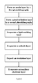
FIG. 2 is a schematic flow chart of a manufacturing method for an OLED component;
FIG. 3 is a schematic layer structure diagram of an OLED component according to a first embodiment of the disclosure;
FIG. 4 is a schematic layer structure diagram of an OLED component according to a second embodiment of the disclosure;
FIG. 5 is a schematic layer structure diagram of an OLED display panel according to a third embodiment of the disclosure.
FIG. 6 is a schematic flow chart of a manufacturing method for an OLED component according to a fourth embodiment of the disclosure;
FIG. 7 is a schematic plan view of an OLED display panel after a transparent electrode layer is formed above a substrate in the method shown in FIG. 6;
FIG. 8 is a schematic plan view of the OLED display panel after a pixel definition layer is formed in the method shown in FIG. 6;
FIG. 9 is a schematic plan view of the OLED display panel after a light-emitting layer and a reflective electrode layer are formed in the method shown in FIG. 6;
FIG. 10 is a schematic layer structure diagram of the OLED component in the OLED display panel after the light-emitting layer and the reflective electrode layer are formed in the method shown in FIG. 6; and
FIG. 11 is a schematic block diagram of a display device including a display panel.
DETAILED DESCRIPTION
In order to make the technical solutions and advantages of the embodiments of the disclosure clearer, the technical solutions of the embodiments of the disclosure will be clearly and fully described below in conjunction with the accompanying drawings. It is obvious that the described embodiments are part, instead of all, of the embodiments of the disclosure. All other embodiments obtained by those skilled in the art based on the described embodiments of the disclosure without the need for creative labor also fall within the scope of the disclosure.
FIG. 1 is a schematic layer structure diagram of an OLED component. As shown in FIG. 1, the OLED component includes an auxiliary electrode layer 6, an insulation layer 4, a transparent electrode layer 1, a light-emitting layer 2 and a reflective electrode layer 3 which are sequentially layered. The insulation layer 4 is arranged with a via such that the transparent electrode layer 1 and the auxiliary electrode layer 6 are connected. In general, when the transparent electrode layer 1 is made of a conductive ITO material, the OLED component is plated with a layer of highly conductive metal to form the auxiliary electrode layer 6, so as to improve the conductivity uniformity of the transparent electrode layer 1 and solve the problem that the luminance of the OLED component, especially a large-sized one, is uneven. The material of the auxiliary electrode layer 6 can be Cr, Mo/Al/Mo, Ag, etc., with good electrical conductivity and less square resistance. Due to the existence of the auxiliary electrode layer 6, the luminance uniformity of the OLED display panel is greatly improved, and this manner can also be applied to a white organic light-emitting diode (WOLED) panel.
However, in general, the auxiliary electrode layer 6 is made of an opaque metal material, and light can not pass through. The auxiliary electrode layer 6 needs to cover the transparent electrode layer 1 in an interconnected mesh structure, which blocks the light emitted by the OLED component. Therefore, after the auxiliary electrode layer 6 is added, a larger drive current is required in order to maintain the same luminance, which increases power consumption and cost. In addition, this also reduces the aperture ratio of the display panel using the OLED component.
FIG. 2 is a schematic flow chart of a manufacturing method for an OLED component. As shown in FIG. 2, the manufacturing method for an OLED component includes: forming an auxiliary electrode layer by a first photolithography, forming an insulation layer by a second photolithography, forming an anode layer by a third photolithography, evaporating a light-emitting layer and evaporating a cathode layer, so as to obtain the structure shown in FIG. 1. In order to obtain interconnected meshes to improve light transmittance as far as possible, a photolithography manner is used in forming the auxiliary electrode layer 6. An etching process is required during the photolithography, and the cost is increased.
Embodiments of the disclosure provide an OLED component. The OLED component includes a first electrode layer 1, a light-emitting layer 2, a second electrode layer 3 and an insulation layer 4 arranged in sequence. The OLED component further includes an auxiliary electrode layer 6 arranged above the insulation layer 4 and electrically connected to the transparent electrode layer 1. Hereinafter, the description will be given by example of the first electrode layer 1 as a transparent electrode layer and the second electrode layer 3 as a reflective electrode layer. It should be understood that this is not a limitation of the present invention.
The light emitted by the OLED component is emitted from the light-emitting layer 2 toward the transparent electrode layer 1, while the auxiliary electrode layer 6 is located in the opposite direction. Thus, the auxiliary electrode layer 6 does not block the light emitted from the OLED component. According to embodiments of the disclosure, the luminance of the OLED display panel will not be changed while the luminance uniformity of the OLED display panel is improved. The transparent electrode layer 1 can be an anode layer, and in this case, the reflective electrode layer 3 is a cathode layer. The transparent electrode layer 1 can be a cathode layer, and in this case, the reflective electrode layer 3 is an anode layer.
FIG. 3 is a schematic layer structure diagram of an OLED component provided according to a first embodiment of the disclosure. As shown in FIG. 3, in embodiments of the disclosure, the OLED component includes a transparent electrode layer 1, a pixel definition layer 5, a light-emitting layer 2, a reflective electrode layer 3 and an insulation layer 4. The pixel definition layer 5 is arranged above the transparent electrode layer 1, and defines a pixel definition region. The light-emitting layer 2, the reflective electrode layer 3 and the insulation layer 4 are arranged above the transparent electrode layer 1 in sequence and arranged in the pixel definition region. The OLED component further includes an auxiliary electrode layer 6 arranged above the insulation layer 4 and connected to the transparent electrode layer 1 through the via 7 of the pixel definition layer 5.
The light emitted by the OLED component is emitted from the light-emitting layer 2 toward the transparent electrode layer 1 while the auxiliary electrode layer 6 is located in the opposite direction. Thus, the auxiliary electrode layer 6 does not block the light emitted from the OLED component. According to embodiments of the disclosure, the luminance of the OLED display panel will not be changed while the luminance uniformity of the OLED display panel is improved.
In addition, as shown in FIG. 3, the insulation layer 4 is provided in the pixel definition region and can be formed using the same or similar mask as the light-emitting layer 2 and the reflective electrode layer 3, simplifying the manufacturing process.
FIG. 4 is a schematic layer structure diagram of an OLED component provided according to a second embodiment of the disclosure. In embodiments of the disclosure, the insulation layer 4 is arranged in the pixel definition region and above the pixel definition layer 5, and has a via 8. The insulation layer 4 can be extended for packaging the OLED component. In this case, the insulation layer 4 has the via 8 above the via 7. The via 7 and the via 8 enable the electrical connection between the auxiliary electrode layer 6 and the transparent electrode layer 1.
FIG. 5 is a schematic layer structure diagram of an OLED display panel provided according to a third embodiment of the disclosure. In embodiments of the disclosure, the OLED display panel includes a substrate 9 and a plurality of the above-described OLED components arranged above the substrate 9. A plurality of OLED components shown in FIG. 3 are shown in FIG. 5, but it can be understood that the OLED components in FIG. 5 can also be OLED components shown in FIG. 4.
The auxiliary electrode layer does not block the light emitted by the OLED component. Therefore, during manufacturing the OLED display panel, the auxiliary electrode layer of the entire panel can be formed into any pattern without being limited to the grid structure. In this way, not only can the square resistance be further reduced and the luminance uniformity be improved, the etching process may be also removed, and the manufacturing method is simplified.
FIG. 6 is a schematic flow chart of a manufacturing method for an OLED component provided according to a fourth embodiment of the disclosure. FIG. 7 is a schematic plan view of the OLED display panel after the transparent electrode layer is formed above the substrate in the method shown in FIG. 6. FIG. 8 is a schematic plan view of the OLED display panel after the pixel definition layer is formed in the method shown in FIG. 6. FIG. 9 is a schematic plan view of the OLED display panel after the light-emitting layer and the reflective electrode layer are formed in the method shown in FIG. 6. FIG. 10 is a schematic layer structure diagram of the OLED component in the OLED display panel after the light-emitting layer and the reflective electrode layer are formed in the method shown in FIG. 6.
As shown in FIG. 6, in embodiments of the disclosure, a manufacturing method for an OLED component is used to manufacture the above OLED component. The method includes: forming a transparent electrode layer 1; forming a pixel definition layer 5 above the transparent electrode layer 1, wherein the definition layer 5 defines a pixel definition region, and the pixel definition layer 5 has a via 7; forming a light-emitting layer 2 and a reflection electrode layer 3 above the transparent electrode layer 1 and in the pixel definition region; forming an insulation layer 4 above the reflection electrode layer 3 and in the pixel definition region; forming an auxiliary electrode layer 6 above the insulation layer 4, wherein the auxiliary electrode layer 6 and the transparent electrode layer 1 are electrically connected through the via 7 of the pixel definition layer 5.
In embodiments of the disclosure, the insulation layer 4 is arranged in the pixel definition region and can be formed using the same or similar mask as the light-emitting layer 2 and the reflective electrode layer 3, thereby simplifying the manufacturing process.
In embodiments of the disclosure, during forming the insulation layer 4, the insulation layer 4 may also be arranged in the pixel definition region and above the pixel definition layer 5, and the insulation layer 4 may include a via 8 located above the via 7. During forming the auxiliary electrode layer 6, the auxiliary electrode layer 6 and the transparent electrode layer 1 are electrically connected through the via of the insulation layer 4 and the via of the pixel definition layer 5. In this way, the insulation layer 4 can be extended for packaging the OLED component. In this case, the insulation layer 4 has the via 8, and the via 7 and the via 8 enable the connection between the auxiliary electrode layer 6 and the transparent electrode layer 1.
In embodiments of the disclosure, the auxiliary electrode layer 6 can be formed using an evaporation method, in particular, an evaporation method adopting an open mask. In addition, a fine metal mask may also be used.
The evaporation method using the mask can include the following steps. First, a mask having an open region is coated on a surface to be evaporated on. Then, the surface is evaporated on. At this time, the material is evaporated at a position corresponding to the open region of the mask on the surface, while the other position is covered and the material is not evaporated thereon. In this way, the auxiliary electrode layer 6 of a predetermined pattern can be obtained by one evaporation without etching.
Of course, the entire auxiliary electrode layer 6 can also be obtained by direct evaporation if necessary.
As shown in FIG. 7, in embodiments of the disclosure, the transparent electrode layer 1 of the OLED component may use an ITO material, and the transparent electrode layer 1 for a plurality of OLED components can be obtained on the OLED display panel by patterning with photolithography.
As shown in FIG. 8, the pixel definition layer 5 of the OLED component is formed, and the pixel definition layer 5 defines a plurality of regions corresponding to the transparent electrode layer 1 for the plurality of OLED components for forming the plurality of OLED components. There is a via 7 left in the pixel definition layer 5 for the connection between the auxiliary electrode layer 6 and the transparent electrode layer 1.
As shown in FIG. 9 and FIG. 10, in embodiments of the disclosure, the light-emitting layer 2 and the reflective electrode layer 3 are evaporated in sequence above the transparent electrode layer using an evaporation method adopting an open mask. In addition, the material of the reflective electrode layer 3 can be Al. Between the transparent electrode layer 1 and the reflective electrode layer 3, a light-emitting functional layer such as a hole injection layer, a hole transport layer, an electron injection layer, etc. (not shown) can be further included.
Finally, referring back to FIG. 3 or FIG. 4, in embodiments of the disclosure, the insulation layer 4 can be deposited by a chemical vapor deposition (CVD) method for isolating the reflective electrode layer 3 from the auxiliary electrode layer 6. As shown in FIG. 4, the insulation layer 4 can also function to package the OLED component. The insulation layer 4 may be a ceramic film such as SiNx or SiO2. In addition, an open mask is also used for depositing the insulation layer 4. When the insulation layer 4 is further arranged above the pixel definition layer, the pattern of the open mask can cover the corresponding positions of the via 7 and the via 8 to form the via 8 and retain the via 7, which enables the auxiliary electrode layer 6 to be connected to the transparent electrode layer 1 through the via 8 of the insulation layer 4 and the via 7 of the pixel definition layer 5.
In embodiments of the disclosure, it is ensured during manufacturing that neither the evaporated layer nor the deposited layer (including the light-emitting layer 2, the reflective electrode layer 3 and the insulation layer 4) in the pixel definition region covers the via 7 arranged in advance at the pixel definition layer 5, to ensure the connection between the auxiliary electrode layer 6 and the transparent electrode layer 1.
FIG. 11 is a schematic block diagram of a display device including a display panel.
The OLED component and the OLED display panel 1101 provided in embodiments of the disclosure can be applied to an OLED display device 1102. The OLED display device 1102 can be any product or component with a display function, such as a mobile phone, a tablet computer, a television, a display, a notebook computer, a digital photo frame, a navigator, etc.
In embodiments of the disclosure, after the reflective electrode layer 3 is evaporated, the insulation layer 4 is deposited, the auxiliary electrode layer 6 is evaporated on the insulation layer 4, and the auxiliary electrode layer 6 is connected to the transparent electrode layer 1 through the via 7, which can reduce the voltage drop of the transparent electrode layer 1, and will not affect light output. The auxiliary electrode layer 6 does not need to be etched into a grid structure and can be evaporated on the entire surface, removing the etching process, further simplifying the manufacturing process of the OLED component and improving the production efficiency of the OLED component.
It can be understood that the above embodiments are merely exemplary embodiments used for illustrating the principle of the disclosure, but the disclosure is not limited thereto. For those of ordinary skill in the art, various variations and improvements can be made without departing from the spirit and essence of the disclosure, and these variations and improvements also fall within the protection scope of the disclosure.

Claims (20)

What is claimed is:
1. An organic light-emitting diode component comprising a first electrode layer, a light-emitting layer and a second electrode layer, in sequence;
wherein the organic light-emitting diode component further comprises an insulation layer, an auxiliary electrode layer and a pixel definition layer;
wherein the insulation layer is positioned above the second electrode layer;
wherein the auxiliary electrode layer is positioned above the insulation layer and electrically connected to the first electrode layer;
wherein the pixel definition layer is positioned above the first electrode layer, and includes a plurality of open regions;
wherein an open region of the plurality of open regions corresponds to a pixel definition region; and
wherein the light-emitting layer and the second electrode layer are positioned in the pixel definition region.
2. The organic light-emitting diode component according to claim 1,
wherein the insulation layer is positioned in the pixel definition region;
wherein the pixel definition layer includes via; and
wherein the auxiliary electrode layer is electrically connected to the first electrode layer through the via of the pixel definition layer.
3. The organic light-emitting diode component according to claim 2, wherein the first electrode layer is an anode layer and the second electrode layer is a cathode layer.
4. The organic light-emitting diode component according to claim 2, wherein the first electrode layer is a transparent electrode layer and the second electrode layer is a reflective electrode layer.
5. A The display panel comprising:
a substrate; and
a plurality of organic light-emitting diode components positioned above the substrate, the plurality of organic light-emitting diode components including the organic light-emitting diode component according to claim 2.
6. The organic light-emitting diode component according to claim 1,
wherein the insulation layer is positioned in the pixel definition region and above the pixel definition layer;
wherein the pixel definition layer includes a via, and the insulation layer includes a via;
wherein the via of the insulation layer is positioned above the via of the pixel definition layer; and
wherein the auxiliary electrode layer is electrically connected to the first electrode layer through the via of the insulation layer and the via of the pixel definition layer.
7. The organic light-emitting diode component according to claim 6, wherein the first electrode layer is an anode layer and the second electrode layer is a cathode layer.
8. The organic light-emitting diode component according to claim 6, wherein the first electrode layer is a transparent electrode layer and the second electrode layer is a reflective electrode layer.
9. A display panel comprising:
a substrate; and
a plurality of organic light-emitting diode components positioned above the substrate, the plurality of organic light-emitting diode components including the organic light-emitting diode component according to claim 6.
10. The organic light-emitting diode component according to claim 1, wherein the first electrode layer is an anode layer and the second electrode layer is a cathode layer.
11. The organic light-emitting diode component according to claim 1, wherein the first electrode layer is a transparent electrode layer and the second electrode layer is a reflective electrode layer.
12. A display panel comprising:
a substrate; and
a plurality of organic light-emitting diode components positioned above the substrate, the plurality of organic light-emitting diode components including the organic light-emitting diode component according to claim 1.
13. A display device comprising the display panel according to claim 12.
14. A manufacturing method for an organic light-emitting diode component, the method comprising:
forming a first electrode layer;
forming a pixel definition layer above the first electrode layer, the pixel definition layer including a via and a plurality of open regions, an open region of the plurality of open regions corresponding to a pixel definition region;
forming a light-emitting layer and a second electrode layer above the first electrode layer and in the pixel definition region;
forming an insulation layer above the second electrode layer and in the pixel definition region; and
forming an auxiliary electrode layer above the insulation layer, the auxiliary electrode layer and the first electrode layer electrically connected through the via of the pixel definition layer.
15. The manufacturing method according to claim 14,
wherein forming the insulation layer includes forming the insulation layer above the pixel definition layer;
wherein the insulation layer includes a via above the via of the pixel definition layer; and
wherein forming the auxiliary electrode layer includes forming the auxiliary electrode layer so that the auxiliary electrode layer and the first electrode layer are electrically connected through the via of the insulation layer and the via of the pixel definition layer.
16. The manufacturing method according to claim 15, wherein forming the insulation layer includes forming the insulation layer with a chemical vapor deposition method adopting an open mask.
17. The manufacturing method according to claim 15, wherein forming the auxiliary electrode layer includes forming the auxiliary electrode layer with an evaporation method.
18. The manufacturing method according to claim 14, wherein forming the insulation layer includes forming the insulation layer with a chemical vapor deposition method adopting an open mask.
19. The manufacturing method according to claim 14, wherein forming the auxiliary electrode layer includes forming the auxiliary electrode layer with an evaporation method.
20. The manufacturing method according to claim 19, wherein forming the auxiliary electrode layer includes forming the auxiliary electrode layer with the evaporation method adopting an open mask or a fine metal mask.
US15/739,941 2016-08-26 2017-06-26 Organic light-emitting diode components including an insulating layer and an auxiliary electrode layer positioned above the insulating layer, manufacturing methods for organic light-emitting diode components, display panels including organic light-emitting diode components, and display devices Active US10270054B2 (en)

Applications Claiming Priority (4)

Application Number Priority Date Filing Date Title
CN201610743210.9 2016-08-26
CN201610743210.9A CN106252525B (en) 2016-08-26 2016-08-26 OLED and preparation method, display panel and display device
CN201610743210 2016-08-26
PCT/CN2017/089961 WO2018036258A1 (en) 2016-08-26 2017-06-26 Oled device and manufacturing method therefor, display panel, and display apparatus

Publications (2)

Publication Number Publication Date
US20180315948A1 US20180315948A1 (en) 2018-11-01
US10270054B2 true US10270054B2 (en) 2019-04-23

Family

ID=57597154

Family Applications (1)

Application Number Title Priority Date Filing Date
US15/739,941 Active US10270054B2 (en) 2016-08-26 2017-06-26 Organic light-emitting diode components including an insulating layer and an auxiliary electrode layer positioned above the insulating layer, manufacturing methods for organic light-emitting diode components, display panels including organic light-emitting diode components, and display devices

Country Status (5)

Country Link
US (1) US10270054B2 (en)
EP (1) EP3506379A4 (en)
JP (1) JP7051440B2 (en)
CN (1) CN106252525B (en)
WO (1) WO2018036258A1 (en)

Cited By (2)

* Cited by examiner, † Cited by third party
Publication number Priority date Publication date Assignee Title
US11171188B2 (en) * 2017-06-26 2021-11-09 Boe Technology Group Co., Ltd. Organic light-emitting diode device, organic light-emitting diode display apparatus, and preparation method for organic light-emitting diode device
US11930673B2 (en) 2020-03-27 2024-03-12 Boe Technology Group Co., Ltd. Display panel and display device

Families Citing this family (2)

* Cited by examiner, † Cited by third party
Publication number Priority date Publication date Assignee Title
CN106252525B (en) 2016-08-26 2018-03-27 京东方科技集团股份有限公司 OLED and preparation method, display panel and display device
CN106783924B (en) * 2016-12-27 2020-10-27 Tcl科技集团股份有限公司 OLED display panel and manufacturing method thereof

Citations (24)

* Cited by examiner, † Cited by third party
Publication number Priority date Publication date Assignee Title
US20050122043A1 (en) * 2003-11-25 2005-06-09 Yoshifumi Kato Organic electroluminescent element, method of manufacturing the same and lighting unit
US20050253508A1 (en) 2004-05-17 2005-11-17 Sharp Kabushiki Kaisha Organic electroluminescent display element, display device having the same, and manufacturing method of the same
CN1717137A (en) 2004-05-21 2006-01-04 株式会社半导体能源研究所 Lighting device
CN1866537A (en) 2005-05-17 2006-11-22 Lg电子株式会社 Organic electroluminescent device and method for manufacturing the same
CN101131959A (en) 2006-08-23 2008-02-27 索尼株式会社 Display and method for manufacturing the same
CN101728421A (en) 2008-10-29 2010-06-09 索尼株式会社 Organic el display and method of manufacturing the same
CN101911832A (en) 2008-12-18 2010-12-08 松下电器产业株式会社 Organic electroluminescent display device and method for manufacturing same
CN101968948A (en) 2010-09-20 2011-02-09 四川虹视显示技术有限公司 Auxiliary electrode structure for organic light emitting diode (OLED) illuminating panel
US20110215362A1 (en) 2010-03-02 2011-09-08 Kabushiki Kaisha Toshiba Illumination device and method for manufacturing same
CN102544054A (en) 2010-12-14 2012-07-04 三星移动显示器株式会社 Organic light-emitting display device and method of manufacturing the same
JP2012181931A (en) 2011-02-28 2012-09-20 Kaneka Corp Organic el light-emitting element
CN103024960A (en) 2012-11-30 2013-04-03 昆山维信诺显示技术有限公司 Organic light emitting diode (OLED) lighting panel, preparation method and OLED lighting device
CN103137891A (en) 2011-12-01 2013-06-05 群康科技(深圳)有限公司 Organic light-emitting diodes (LEDs) and organic LED displayer composed of the same
CN103219469A (en) 2012-01-20 2013-07-24 财团法人工业技术研究院 Light emitting assembly
CN103296052A (en) 2012-02-29 2013-09-11 群康科技(深圳)有限公司 Display panel and display device
JP2014150030A (en) 2013-02-04 2014-08-21 Mitsubishi Chemicals Corp Organic EL device
CN104022139A (en) 2014-05-30 2014-09-03 京东方科技集团股份有限公司 Organic electroluminescence displaying panel and device
JP2014192050A (en) 2013-03-27 2014-10-06 Kaneka Corp Organic el device and method for manufacturing organic el device
CN104124259A (en) 2013-04-23 2014-10-29 乐金显示有限公司 Organic light emitting diode display device and method of fabricating the same
US20140361264A1 (en) * 2013-06-10 2014-12-11 Samsung Display Co., Ltd. Organic light emitting display device and method of manufacturing the same
CN104885251A (en) 2012-12-28 2015-09-02 乐金显示有限公司 Transparent organic light emitting display device and method for manufacturing the same
CN105470278A (en) 2014-09-26 2016-04-06 乐金显示有限公司 Organic light emitting diode display device and method of fabricating same
CN105470279A (en) 2014-09-11 2016-04-06 乐金显示有限公司 Organic light emitting display device and method of manufacturing same
CN106252525A (en) 2016-08-26 2016-12-21 京东方科技集团股份有限公司 OLED and manufacture method, display floater and display device

Family Cites Families (8)

* Cited by examiner, † Cited by third party
Publication number Priority date Publication date Assignee Title
JP4534430B2 (en) * 2003-04-24 2010-09-01 セイコーエプソン株式会社 Electro-optical device, substrate for electro-optical device, method for manufacturing electro-optical device, and electronic apparatus
JP2009151955A (en) 2007-12-18 2009-07-09 Sony Corp Surface emitting light source and its manufacturing method
DE102008020816B4 (en) 2008-02-29 2019-10-10 Osram Oled Gmbh Organic light-emitting diode, planar, optically active element with a contact arrangement and method for producing an organic light-emitting diode
JP5423325B2 (en) * 2009-11-10 2014-02-19 ソニー株式会社 Light emitting device and manufacturing method thereof
JP5907766B2 (en) 2012-03-14 2016-04-26 株式会社カネカ Light emitting device and method for manufacturing light emitting device
DE102012221191B4 (en) * 2012-11-20 2022-03-17 Pictiva Displays International Limited Optoelectronic component and method for producing an optoelectronic component
CN104867962B (en) * 2015-05-06 2019-04-05 京东方科技集团股份有限公司 A kind of OLED array and preparation method thereof, OLED display
CN105870265A (en) * 2016-04-19 2016-08-17 京东方科技集团股份有限公司 Light-emitting diode substrate and preparation method thereof and display device

Patent Citations (25)

* Cited by examiner, † Cited by third party
Publication number Priority date Publication date Assignee Title
US20050122043A1 (en) * 2003-11-25 2005-06-09 Yoshifumi Kato Organic electroluminescent element, method of manufacturing the same and lighting unit
US20050253508A1 (en) 2004-05-17 2005-11-17 Sharp Kabushiki Kaisha Organic electroluminescent display element, display device having the same, and manufacturing method of the same
CN1717137A (en) 2004-05-21 2006-01-04 株式会社半导体能源研究所 Lighting device
CN1866537A (en) 2005-05-17 2006-11-22 Lg电子株式会社 Organic electroluminescent device and method for manufacturing the same
CN101131959A (en) 2006-08-23 2008-02-27 索尼株式会社 Display and method for manufacturing the same
CN101728421A (en) 2008-10-29 2010-06-09 索尼株式会社 Organic el display and method of manufacturing the same
CN101911832A (en) 2008-12-18 2010-12-08 松下电器产业株式会社 Organic electroluminescent display device and method for manufacturing same
US20110215362A1 (en) 2010-03-02 2011-09-08 Kabushiki Kaisha Toshiba Illumination device and method for manufacturing same
US8368129B2 (en) * 2010-03-02 2013-02-05 Kabushiki Kaisha Toshiba Illumination device and method for manufacturing same
CN101968948A (en) 2010-09-20 2011-02-09 四川虹视显示技术有限公司 Auxiliary electrode structure for organic light emitting diode (OLED) illuminating panel
CN102544054A (en) 2010-12-14 2012-07-04 三星移动显示器株式会社 Organic light-emitting display device and method of manufacturing the same
JP2012181931A (en) 2011-02-28 2012-09-20 Kaneka Corp Organic el light-emitting element
CN103137891A (en) 2011-12-01 2013-06-05 群康科技(深圳)有限公司 Organic light-emitting diodes (LEDs) and organic LED displayer composed of the same
CN103219469A (en) 2012-01-20 2013-07-24 财团法人工业技术研究院 Light emitting assembly
CN103296052A (en) 2012-02-29 2013-09-11 群康科技(深圳)有限公司 Display panel and display device
CN103024960A (en) 2012-11-30 2013-04-03 昆山维信诺显示技术有限公司 Organic light emitting diode (OLED) lighting panel, preparation method and OLED lighting device
CN104885251A (en) 2012-12-28 2015-09-02 乐金显示有限公司 Transparent organic light emitting display device and method for manufacturing the same
JP2014150030A (en) 2013-02-04 2014-08-21 Mitsubishi Chemicals Corp Organic EL device
JP2014192050A (en) 2013-03-27 2014-10-06 Kaneka Corp Organic el device and method for manufacturing organic el device
CN104124259A (en) 2013-04-23 2014-10-29 乐金显示有限公司 Organic light emitting diode display device and method of fabricating the same
US20140361264A1 (en) * 2013-06-10 2014-12-11 Samsung Display Co., Ltd. Organic light emitting display device and method of manufacturing the same
CN104022139A (en) 2014-05-30 2014-09-03 京东方科技集团股份有限公司 Organic electroluminescence displaying panel and device
CN105470279A (en) 2014-09-11 2016-04-06 乐金显示有限公司 Organic light emitting display device and method of manufacturing same
CN105470278A (en) 2014-09-26 2016-04-06 乐金显示有限公司 Organic light emitting diode display device and method of fabricating same
CN106252525A (en) 2016-08-26 2016-12-21 京东方科技集团股份有限公司 OLED and manufacture method, display floater and display device

Non-Patent Citations (3)

* Cited by examiner, † Cited by third party
Title
International Search Report from PCT Application No. PCT/CN2017/089961 dated Sep. 26, 2017 (5 pages).
Office Action from Chinese Application No. 201610743210.9 dated Aug. 2, 2017 (8 pages).
Written Opinion from PCT Application No. PCT/CN2017/089961 dated Sep. 26, 2017 (5 pages).

Cited By (2)

* Cited by examiner, † Cited by third party
Publication number Priority date Publication date Assignee Title
US11171188B2 (en) * 2017-06-26 2021-11-09 Boe Technology Group Co., Ltd. Organic light-emitting diode device, organic light-emitting diode display apparatus, and preparation method for organic light-emitting diode device
US11930673B2 (en) 2020-03-27 2024-03-12 Boe Technology Group Co., Ltd. Display panel and display device

Also Published As

Publication number Publication date
JP7051440B2 (en) 2022-04-11
JP2019531572A (en) 2019-10-31
US20180315948A1 (en) 2018-11-01
EP3506379A4 (en) 2020-03-18
WO2018036258A1 (en) 2018-03-01
CN106252525A (en) 2016-12-21
CN106252525B (en) 2018-03-27
EP3506379A1 (en) 2019-07-03

Similar Documents

Publication Publication Date Title
US10886492B2 (en) Array substrate and display panel comprising fracture opening for blocking carrier transportation between adjacent sub-pixels
CN109244269B (en) Display panel, manufacturing method thereof and display device
US9111888B2 (en) Organic light emitting diode display device
US20210005835A1 (en) Organic electroluminescent display panel, manufacturing method thereof, and display device
CN108461527B (en) Organic electroluminescent display panel, manufacturing method thereof and display device
WO2018233297A1 (en) Organic light-emitting diode display panel and manufacturing method therefor, and display apparatus
US10270054B2 (en) Organic light-emitting diode components including an insulating layer and an auxiliary electrode layer positioned above the insulating layer, manufacturing methods for organic light-emitting diode components, display panels including organic light-emitting diode components, and display devices
CN110890406B (en) Organic light-emitting display back plate, manufacturing method thereof and display device
CN109920816B (en) Display substrate, manufacturing method thereof and display device
US9666658B2 (en) Organic light emitting diode display and manufacturing method thereof
CN106856203B (en) Top-emitting display light-emitting device and preparation method thereof
US11289685B2 (en) Display panel with patterned light absorbing layer, and manufacturing method thereof
KR102185577B1 (en) OLED substrate and its manufacturing method
CN108573998B (en) Display panel, manufacturing method and display device
US20210134900A1 (en) Light emitting substrate and manufacturing method thereof, electronic device
KR102255063B1 (en) Organic Light Emitting Diode Display Device
CN101740726B (en) Organic electroluminescent device and manufacturing method thereof
US20230032598A1 (en) Display panel, display apparatus, and manufacturing method for display panel
US10964755B2 (en) Organic light emitting diode panel including light emitting units and color filter layer, method for manufacturing the same, and display device
US10461136B2 (en) Organic electroluminescent display panel with semiconductor layer, manufacturing method for manufacturing the same, and display device
KR20110081522A (en) Organic light emitting display deviece and the fabricating method of the same
US11723261B2 (en) Light-emitting component, manufacturing method therefor, mask, and display device
CN109103235B (en) Organic light emitting diode display panel, manufacturing method thereof and display device
US20220102669A1 (en) Organic electroluminescent structure and fabrication method thereof, and display device
CN110137233B (en) Array substrate, preparation method thereof and display device

Legal Events

Date Code Title Description
FEPP Fee payment procedure

Free format text: ENTITY STATUS SET TO UNDISCOUNTED (ORIGINAL EVENT CODE: BIG.); ENTITY STATUS OF PATENT OWNER: LARGE ENTITY

AS Assignment

Owner name: BOE TECHNOLOGY GROUP CO., LTD., CHINA

Free format text: ASSIGNMENT OF ASSIGNORS INTEREST;ASSIGNOR:ZHANG, CAN;REEL/FRAME:045013/0144

Effective date: 20171114

STPP Information on status: patent application and granting procedure in general

Free format text: PUBLICATIONS -- ISSUE FEE PAYMENT VERIFIED

STCF Information on status: patent grant

Free format text: PATENTED CASE

MAFP Maintenance fee payment

Free format text: PAYMENT OF MAINTENANCE FEE, 4TH YEAR, LARGE ENTITY (ORIGINAL EVENT CODE: M1551); ENTITY STATUS OF PATENT OWNER: LARGE ENTITY

Year of fee payment: 4