US10241597B2 - Active stylus pen and touch sensing system including the same - Google Patents
Active stylus pen and touch sensing system including the same Download PDFInfo
- Publication number
- US10241597B2 US10241597B2 US15/392,783 US201615392783A US10241597B2 US 10241597 B2 US10241597 B2 US 10241597B2 US 201615392783 A US201615392783 A US 201615392783A US 10241597 B2 US10241597 B2 US 10241597B2
- Authority
- US
- United States
- Prior art keywords
- touch
- pen
- touch screen
- uplink signal
- driving circuit
- Prior art date
- Legal status (The legal status is an assumption and is not a legal conclusion. Google has not performed a legal analysis and makes no representation as to the accuracy of the status listed.)
- Active, expires
Links
Images


Classifications
-
- G—PHYSICS
- G06—COMPUTING; CALCULATING OR COUNTING
- G06F—ELECTRIC DIGITAL DATA PROCESSING
- G06F3/00—Input arrangements for transferring data to be processed into a form capable of being handled by the computer; Output arrangements for transferring data from processing unit to output unit, e.g. interface arrangements
- G06F3/01—Input arrangements or combined input and output arrangements for interaction between user and computer
- G06F3/03—Arrangements for converting the position or the displacement of a member into a coded form
- G06F3/033—Pointing devices displaced or positioned by the user, e.g. mice, trackballs, pens or joysticks; Accessories therefor
- G06F3/038—Control and interface arrangements therefor, e.g. drivers or device-embedded control circuitry
- G06F3/0383—Signal control means within the pointing device
-
- G—PHYSICS
- G06—COMPUTING; CALCULATING OR COUNTING
- G06F—ELECTRIC DIGITAL DATA PROCESSING
- G06F3/00—Input arrangements for transferring data to be processed into a form capable of being handled by the computer; Output arrangements for transferring data from processing unit to output unit, e.g. interface arrangements
- G06F3/01—Input arrangements or combined input and output arrangements for interaction between user and computer
- G06F3/03—Arrangements for converting the position or the displacement of a member into a coded form
- G06F3/033—Pointing devices displaced or positioned by the user, e.g. mice, trackballs, pens or joysticks; Accessories therefor
- G06F3/0354—Pointing devices displaced or positioned by the user, e.g. mice, trackballs, pens or joysticks; Accessories therefor with detection of 2D relative movements between the device, or an operating part thereof, and a plane or surface, e.g. 2D mice, trackballs, pens or pucks
- G06F3/03545—Pens or stylus
-
- G—PHYSICS
- G06—COMPUTING; CALCULATING OR COUNTING
- G06F—ELECTRIC DIGITAL DATA PROCESSING
- G06F3/00—Input arrangements for transferring data to be processed into a form capable of being handled by the computer; Output arrangements for transferring data from processing unit to output unit, e.g. interface arrangements
- G06F3/01—Input arrangements or combined input and output arrangements for interaction between user and computer
- G06F3/03—Arrangements for converting the position or the displacement of a member into a coded form
- G06F3/033—Pointing devices displaced or positioned by the user, e.g. mice, trackballs, pens or joysticks; Accessories therefor
- G06F3/038—Control and interface arrangements therefor, e.g. drivers or device-embedded control circuitry
-
- G—PHYSICS
- G06—COMPUTING; CALCULATING OR COUNTING
- G06F—ELECTRIC DIGITAL DATA PROCESSING
- G06F3/00—Input arrangements for transferring data to be processed into a form capable of being handled by the computer; Output arrangements for transferring data from processing unit to output unit, e.g. interface arrangements
- G06F3/01—Input arrangements or combined input and output arrangements for interaction between user and computer
- G06F3/03—Arrangements for converting the position or the displacement of a member into a coded form
- G06F3/041—Digitisers, e.g. for touch screens or touch pads, characterised by the transducing means
- G06F3/0412—Digitisers structurally integrated in a display
-
- G—PHYSICS
- G06—COMPUTING; CALCULATING OR COUNTING
- G06F—ELECTRIC DIGITAL DATA PROCESSING
- G06F3/00—Input arrangements for transferring data to be processed into a form capable of being handled by the computer; Output arrangements for transferring data from processing unit to output unit, e.g. interface arrangements
- G06F3/01—Input arrangements or combined input and output arrangements for interaction between user and computer
- G06F3/03—Arrangements for converting the position or the displacement of a member into a coded form
- G06F3/041—Digitisers, e.g. for touch screens or touch pads, characterised by the transducing means
- G06F3/0416—Control or interface arrangements specially adapted for digitisers
- G06F3/04162—Control or interface arrangements specially adapted for digitisers for exchanging data with external devices, e.g. smart pens, via the digitiser sensing hardware
-
- G—PHYSICS
- G06—COMPUTING; CALCULATING OR COUNTING
- G06F—ELECTRIC DIGITAL DATA PROCESSING
- G06F3/00—Input arrangements for transferring data to be processed into a form capable of being handled by the computer; Output arrangements for transferring data from processing unit to output unit, e.g. interface arrangements
- G06F3/01—Input arrangements or combined input and output arrangements for interaction between user and computer
- G06F3/03—Arrangements for converting the position or the displacement of a member into a coded form
- G06F3/041—Digitisers, e.g. for touch screens or touch pads, characterised by the transducing means
- G06F3/044—Digitisers, e.g. for touch screens or touch pads, characterised by the transducing means by capacitive means
- G06F3/0441—Digitisers, e.g. for touch screens or touch pads, characterised by the transducing means by capacitive means using active external devices, e.g. active pens, for receiving changes in electrical potential transmitted by the digitiser, e.g. tablet driving signals
-
- G—PHYSICS
- G06—COMPUTING; CALCULATING OR COUNTING
- G06F—ELECTRIC DIGITAL DATA PROCESSING
- G06F3/00—Input arrangements for transferring data to be processed into a form capable of being handled by the computer; Output arrangements for transferring data from processing unit to output unit, e.g. interface arrangements
- G06F3/01—Input arrangements or combined input and output arrangements for interaction between user and computer
- G06F3/03—Arrangements for converting the position or the displacement of a member into a coded form
- G06F3/041—Digitisers, e.g. for touch screens or touch pads, characterised by the transducing means
- G06F3/044—Digitisers, e.g. for touch screens or touch pads, characterised by the transducing means by capacitive means
- G06F3/0442—Digitisers, e.g. for touch screens or touch pads, characterised by the transducing means by capacitive means using active external devices, e.g. active pens, for transmitting changes in electrical potential to be received by the digitiser
-
- G—PHYSICS
- G06—COMPUTING; CALCULATING OR COUNTING
- G06F—ELECTRIC DIGITAL DATA PROCESSING
- G06F3/00—Input arrangements for transferring data to be processed into a form capable of being handled by the computer; Output arrangements for transferring data from processing unit to output unit, e.g. interface arrangements
- G06F3/01—Input arrangements or combined input and output arrangements for interaction between user and computer
- G06F3/03—Arrangements for converting the position or the displacement of a member into a coded form
- G06F3/041—Digitisers, e.g. for touch screens or touch pads, characterised by the transducing means
- G06F3/044—Digitisers, e.g. for touch screens or touch pads, characterised by the transducing means by capacitive means
- G06F3/0443—Digitisers, e.g. for touch screens or touch pads, characterised by the transducing means by capacitive means using a single layer of sensing electrodes
-
- G—PHYSICS
- G06—COMPUTING; CALCULATING OR COUNTING
- G06F—ELECTRIC DIGITAL DATA PROCESSING
- G06F3/00—Input arrangements for transferring data to be processed into a form capable of being handled by the computer; Output arrangements for transferring data from processing unit to output unit, e.g. interface arrangements
- G06F3/01—Input arrangements or combined input and output arrangements for interaction between user and computer
- G06F3/03—Arrangements for converting the position or the displacement of a member into a coded form
- G06F3/041—Digitisers, e.g. for touch screens or touch pads, characterised by the transducing means
- G06F3/044—Digitisers, e.g. for touch screens or touch pads, characterised by the transducing means by capacitive means
- G06F3/0446—Digitisers, e.g. for touch screens or touch pads, characterised by the transducing means by capacitive means using a grid-like structure of electrodes in at least two directions, e.g. using row and column electrodes
-
- G—PHYSICS
- G06—COMPUTING; CALCULATING OR COUNTING
- G06F—ELECTRIC DIGITAL DATA PROCESSING
- G06F3/00—Input arrangements for transferring data to be processed into a form capable of being handled by the computer; Output arrangements for transferring data from processing unit to output unit, e.g. interface arrangements
- G06F3/01—Input arrangements or combined input and output arrangements for interaction between user and computer
- G06F3/03—Arrangements for converting the position or the displacement of a member into a coded form
- G06F3/041—Digitisers, e.g. for touch screens or touch pads, characterised by the transducing means
- G06F3/0416—Control or interface arrangements specially adapted for digitisers
- G06F3/04166—Details of scanning methods, e.g. sampling time, grouping of sub areas or time sharing with display driving
Definitions
- the present disclosure relates to a touch sensing system and, more particularly, to a touch sensing system allowing for a touch input through an active stylus pen.
- User interface is configured so that users are able to communicate with various electronic devices and thus can easily and comfortably control the electronic devices as they desire.
- Examples of the user interface include a keypad, a keyboard, a mouse, an on-screen display (OSD), and a remote controller having an infrared communication function or a radio frequency (RF) communication function.
- RF radio frequency
- the touch UI has been adopted for use in a variety of portable information appliances.
- the touch UI is implemented by forming a touch screen on the screen of a display device.
- the touch screen may be implemented as a capacitive touch screen.
- the touch screen having capacitive touch sensors senses changes (i.e., changes in charges of the touch sensor) in a capacitance resulting from an input of a touch driving signal when a user touches (or approaches) the touch sensor with his or her finger or a conductive material, and thus detects a touch input.
- a capacitive touch sensor may be implemented as a self-capacitance sensor or a mutual capacitance sensor. Electrodes of the self-capacitance sensor may be connected to sensor lines formed in one direction, respectively. The mutual capacitance sensor may be formed in intersections of sensor lines perpendicular to each other with a dielectric layer interposed therebetween.
- Stylus pens have been commonly used as human interface devices (HIDs), as well as fingers, in smartphones, smart books, and the like.
- Stylus pens advantageously allow more specific inputs than fingers.
- Stylus pens include a passive stylus pen and an active stylus pen.
- the passive stylus pen is difficult to detect a touch position due to a small change in capacitance in a contact point on a touch screen.
- the active stylus pen is easy to detect a touch position because the active stylus pen generates a driving signal and outputs the generated driving signal to a contact point on the touch screen.
- a touch sensing system including such an active stylus pen operates as follows.
- a touch screen driving signal is applied to a touch screen.
- the touch screen driving signal includes an uplink signal for synchronization with an active stylus pen and a touch sensor driving signal for sensing a touch input applied to the touch screen.
- the active stylus pen receives an uplink signal from the touch screen, generates a downlink signal (hereinafter, referred to as a “pen driving signal”) in synchronization with the touch sensor driving signal on the basis of the uplink signal, and outputs the generated pen driving signal to the touch screen through a conductive tip.
- the pen driving signal is synchronized with the touch sensor driving signal, it serves to increase sensitivity of the touch sensor driving signal.
- the touch sensing system senses a touch input by sensing a change in capacitance in a touch point based on the touch sensor driving signal and the pen driving signal.
- the active stylus pen fails to receive an uplink signal.
- the palm may be either a palm of a hand gripping the stylus pen or a hand without the stylus pen.
- the active stylus pen may fail to be synchronized with the touch screen so it is impossible to perform a normal operation.
- a first reason why the active stylus pen cannot receive an uplink signal is because, when the palm touches the touch screen, a load of the touch screen is increased to attenuate a magnitude of the uplink signal.
- a second reason why the active stylus pen cannot receive the uplink signal is because, when the palm touches the touch screen, an uplink signal is transferred to a housing serving as a ground of the active stylus pen, and thus, the active stylus pen is not able to recognize the uplink signal received through the conductive tip due to interference of the uplink signal received through the housing.
- a touch driving device generates an uplink signal using input power Vin and applies the generated uplink signal to the touch screen.
- a quantity of electric charges transferred to the touch screen as illustrated in FIG. 2A is Qin and a load of the touch screen is Cpl
- a magnitude Vp of the uplink signal detected from the touch screen is Qin/Cpl.
- a load Chl of the human body is added to the load Cpl of the touch screen as illustrated in FIG. 2B .
- the magnitude Vp of the uplink signal is reduced by a magnitude of the load Chl of the human body added to the load Cpl of the touch screen. That is, the magnitude Vp of the uplink signal detected from the touch screen is Qin/Cpl+Chl. Since capacitance of a capacitor is proportional to an area, as a contact area between the touch screen and the palm is increased, the load Chl of the human body is increased and the magnitude Vp of the uplink signal detected from the touch screen is decreased.
- an uplink signal is transferred to the housing of the active stylus pen through the human body.
- the palm may be either the hand gripping the pen or the other hand, and a magnitude of the uplink signal transferred to the human body is proportional to a contact area between the touch screen and the palm.
- (A) of FIG. 5 illustrates the uplink signal applied to the touch screen
- (B) of FIG. 5 illustrates the uplink signal detected from the human body.
- the contact area of the palm is increased, the uplink signal detected from the human body is increased, and the uplink signal is transferred to the housing of the active stylus pen.
- the active stylus pen receives the uplink signal from the touch screen through pen capacitor Cp formed between the conductive tip and the touch screen as illustrated in FIG. 4 , and here, when the palm touches the touch screen, the uplink signal is further received through human capacitor Ch formed between the housing of the pen and the touch screen.
- the pen driving circuit receives the uplink signal simultaneously from both the conductive tip connected to a positive (+) terminal and the housing (ground) connected to a negative ( ⁇ ) terminal as illustrated in FIG. 9 , and thus, it is impossible to normally recognize the uplink signal.
- the uplink signal detected from the touch screen is reduced as illustrated in (A) of FIG. 7 and a ground waveform (i.e., an uplink signal detected from an external case of the touch sensing system) is increased in an out-of-phase manner with respect to the uplink signal (A).
- a ground waveform i.e., an uplink signal detected from an external case of the touch sensing system
- an out-of-phase uplink signal is transferred to the housing of the pen through the human body.
- the out-of-phase uplink signal transferred to the housing of the pen lowers a recognition rate of the uplink signal received through the conductive tip.
- the touch driving device drives an uplink signal to apply input electric charges Qin to the touch screen.
- positive electric charges +Qin are accumulated in one electrode (left electrode) of a panel capacitor Cpanel formed in the touch screen
- negative electric charges ⁇ Qin are accumulated in the other electrode of the panel capacitor Cpanel.
- FIG. 6B when the palm touches the touch screen, a human capacitor Chuman is further connected to the touch screen.
- first negative electric charges ⁇ Qpanel corresponding to negative electric charges ⁇ Qin remain in one electrode (left electrode) of the panel capacitor Cpanel
- second negative electric charges ⁇ Qhuman corresponding to the remainder of the negative electric charges ⁇ Qin are stored in the human capacitor Chuman.
- the capacitor since the capacitor has qualities of storing the same amount of electric charges at both ends thereof, only first positive electric charges +Qpanel remain in one electrode of the panel capacitor Cpanel and the other remaining positive electric charges +(Qin-Qpanel) are pushed out toward a ground GND of the touch sensing system. As a result, an out-of-phase uplink signal is applied to the ground GND connected to the external case of the touch sensing system.
- FIG. 9 is a view illustrating a structure of an active stylus pen in terms of a pen driving circuit when the palm touches the touch screen.
- a receiving unit of the pen driving circuit may include an amplifier having a positive (+) input terminal connected to the conductive tip and a negative ( ⁇ ) input terminal connected to a ground GND.
- the negative ( ⁇ ) input terminal is connected to the touch screen through a human capacitor Ch, the active stylus pen has no choice but to be significantly affected by external noise input from the touch screen.
- An aspect of the present disclosure provides an active stylus pen being insensitive to external noise and having enhanced sensing performance with respect to an uplink signal input from a touch screen, regardless of whether a palm touches the touch screen, and a touch sensing system including the same.
- an active stylus pen includes: a housing connected to an electrical ground; a conductive tip protruding outwardly from one side (e.g., from an end) of the housing and operably brought into contact with a touch screen; a conductor layer surrounding an outer surface of the housing with an insulator interposed therebetween; a pen driving circuit connected to the conductor layer; and a switch that selectively couples the conductor layer and the pen driving circuit.
- the pen driving circuit may be cased (or housed) by the housing, receive an uplink signal and a touch sensor driving signal from the touch screen, generate a pen driving signal synchronized with the touch sensor driving signal and output the generated pen driving signal to the touch screen through the conductive tip.
- At least one touch period of one frame may be allocated to drive the touch screen, and the switch may be switched on during a reception section for inputting the uplink signal within the touch period to connect the conductor layer and the pen driving circuit, and switched off during a transmission section for outputting the pen driving signal within the touch period to release (i.e., to decouple) the electrical connection between the conductor layer and the pen driving circuit.
- the conductive tip may be coupled to the touch screen through a pen capacitor or capacitance, and the conductor layer may be coupled to the touch screen through a human capacitor or capacitance.
- the pen driving circuit may receive the uplink signal through at least one of the conductive tip and the conductor layer.
- the switch When at least one touch period of one frame is allocated to drive the touch screen and the uplink signal is continuously applied in in-phase to the touch screen during the touch period, the switch may be switched on during a reception section for inputting the uplink signal within the touch period, and when the uplink signal is input in out-of-phase to the pen driving circuit within the reception section, the switch may be switched off.
- the switch may be maintained in an ON state during a reception section for inputting the uplink signal within the touch period.
- a touch sensing system includes: a touch screen; a touch driving device applying an uplink signal and a touch sensor driving signal to the touch screen; and an active stylus pen generating a pen driving signal synchronized with the touch sensor driving signal and outputting the generated pen driving signal to the touch screen.
- the active stylus pen may include: a housing connected to an electrical ground; a conductive tip protruding outwardly from one side of the housing and brought into contact with the touch screen; a conductor layer surrounding an outer surface of the housing with an insulator interposed therebetween; a pen driving circuit receiving the uplink signal and the touch sensor driving signal from the touch screen, outputting the pen driving signal to the touch screen through the conductive tip, and cased by the housing; and a switch connecting the conductor layer and the pen driving circuit.
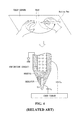
- FIG. 1 is a view illustrating a state in which a palm touches a touch screen, together with an active stylus pen, as may be known in the related art.
- FIGS. 2A, 2B, and 3 are views illustrating an example in which a related art active stylus pen fails to receive an uplink signal.
- FIGS. 4, 5, 6A, 6B, 7, 8A and 8B are views illustrating another example in which a related art active stylus pen fails to receive an uplink signal.
- FIG. 9 is a view illustrating the vulnerability to external noise of the related art active stylus pen.
- FIG. 10 is a view schematically illustrating a touch sensing system according to an embodiment of the present disclosure.
- FIG. 11 is a view illustrating a display device to which a touch sensing system according to an embodiment of the present disclosure is applied.
- FIG. 12 is a view illustrating an example of a touch screen implemented by a mutual capacitance sensor.
- FIG. 13 is a view illustrating an example of a touch screen implemented by a self-capacitance sensor.
- FIG. 14 is a view illustrating an example of a touch sensor installed in a pixel array.
- FIG. 15 is a timing diagram illustrating a method for driving pixels and touch sensors of a display panel in a time-division manner.
- FIG. 16 is a view schematically illustrating a configuration of an active stylus pen according to an embodiment of the present disclosure.
- FIG. 17 is a view illustrating major components of an active stylus pen insensitive to external noise and enhancing detection performance (or sensing performance) with respect to an uplink signal.
- FIG. 18 is a view illustrating a principle of canceling out external noise by a conductor layer provided in an active stylus pen.
- FIGS. 19A and 19B are views illustrating reception paths of an uplink signal in a reception section of one touch period in the presence of palm contact and without palm contact.
- FIG. 19C is a view illustrating a transmission path of a pen driving signal in a transmission section of one touch period.
- FIG. 20 is a view illustrating an ON/OFF state of a switch in each of a reception section and a transmission section of one touch period.
- FIG. 21 is a view illustrating a driving scheme allowing an active stylus pen to easily recognize an out-of-phase uplink signal when the uplink signal is received by the pen.
- FIG. 22 is a view illustrating another driving scheme allowing an active stylus pen to easily recognize an out-of-phase uplink signal when the uplink signal is received by the pen.
- FIG. 10 is a view schematically illustrating a touch sensing system according to an embodiment of the present disclosure.
- the touch sensing system includes a display device 10 and an active stylus pen 20 .
- the display device 10 has a display function and a touch detection function.
- the display device 10 allowing for touch detection according to contact of a conductive object such as a finger and/or the active stylus pen 20 , has an integrated capacitive touch screen.
- the touch screen may be configured independently from a display panel for implementing display, or may be installed in a pixel array of the display panel.
- a touch screen driving signal is applied to the touch screen.
- the touch screen driving signal includes an uplink signal for synchronization with the active stylus pen 20 and a touch sensor driving signal for sensing a touch input applied to the touch screen.
- the active stylus pen 20 generates a pen driving signal synchronized with the touch sensor driving signal on the basis of the uplink signal received by the touch screen and outputs the pen driving signal to a contact point of the touch screen to allow a pen touch input to be easily detected on the touch screen.
- the active stylus pen 20 further include a conductor layer on an outer surface of a housing, and by connecting the conductor layer to a pen driving circuit, even when a palm touches the touch screen, a reception path regarding the touch screen driving signal may be secured and the pen driving circuit may easily receive an uplink signal.
- a switch may be provided between the conductor layer and the pen driving circuit and turned on and off according to conditions.
- the touch sensing system senses a position of a touch input by a conductive object by analyzing touch row data according to the touch sensor driving signal and the pen driving signal on the touch screen.
- the touch sensing system may simultaneously sense a finger touch input by a finger and a pen touch input by the active stylus pen 20 .
- the finger touch input may be sensed on the basis of an analysis result of the touch row data according to the touch sensor driving signal
- the pen touch input may be sensed on the basis of an analysis result of touch row data according to the pen driving signal.
- the pen driving signal and the touch sensor driving signal have the same phase and a magnitude (pulse amplitude) of the pen driving signal is set to be greater than that of the touch sensor driving signal, whereby the touch row data of the position that the pen has touched and the touch row data of the position that the finger has touched are differentiated to easily distinguish between the pen touch input and the finger touch input.
- FIG. 11 illustrates a display device to which a touch sensing system according to an embodiment of the present disclosure is applied.
- FIG. 12 illustrates an example of a touch screen implemented by a mutual capacitance sensor.
- FIG. 13 illustrates an example of a touch screen implemented by a self-capacitance sensor.
- FIG. 14 illustrates an example of a touch sensor installed in a pixel array.
- FIG. 15 illustrates a method for driving pixels and touch sensors of a display panel in a time-division manner.
- the display device 10 may be implemented on the basis of a flat display device such as a liquid crystal display (LCD), a field emission display (FED), a plasma display panel (PDP), an organic light emitting display device, an electrophoresis display, and the like.
- a flat display device such as a liquid crystal display (LCD), a field emission display (FED), a plasma display panel (PDP), an organic light emitting display device, an electrophoresis display, and the like.
- LCD liquid crystal display
- FED field emission display
- PDP plasma display panel
- organic light emitting display device an electrophoresis display, and the like.
- the display device implemented as an LCD will be described, but the display device of the present disclosure is not limited thereto.
- the display device 10 includes a display module and a touch module.
- the touch module included in the display device 10 includes a touch screen TSP and a touch driving device 18 .
- the touch screen TSP may be implemented as a capacitive touch screen sensing a touch input through a plurality of capacitance sensors.
- the touch screen TSP includes a plurality of touch sensors having capacitance.
- Capacitance may be classified as self-capacitance and mutual capacitance.
- the self-capacitance may be formed along a conductor line of a single layer formed in one direction.
- the mutual capacitance may be formed between two conductor lines perpendicular to each other.
- the touch screen TSP implemented by mutual capacitance sensors Cm may include Tx electrode lines, Rx electrode lines intersecting with the Tx electrode lines, and touch sensors Cm formed at intersections of the Tx electrode lines and the Rx electrode lines.
- the Tx electrode lines are driving signal lines supplying electric charges to the touch sensors by applying a touch sensor driving signal (and/or a pen driving signal) to the touch sensors Cm.
- the Rx electrode lines are sensor lines connected to the touch sensors Cm and supplying electric charges of the touch sensors Cm to the touch driving device 18 .
- a mutual capacitance sensing method electric charges are supplied to the touch sensor Cm by applying the touch sensor driving signal (and/or the pen driving signal) to the Tx electrodes through the Tx electrode lines, and a change in capacitance of the touch sensors Cm is sensed through Rx electrodes and the Rx electrode lines in synchronization with the touch sensor driving signal (and/or the pen driving signal, whereby a touch input by a conductive object may be recognized.
- electrodes 31 may be connected to sensor lines 32 formed in one direction, respectively.
- the self-capacitance sensors Cs include capacitance formed in each of the electrodes 31 .
- a touch sensor driving signal and/or the pen driving signal
- electric charges Q are accumulated in the touch sensors Cs.
- parasitic capacitance Cf is additionally connected to the self-capacitance sensor Cs, causing a total capacitance value to be changed.
- the touch screen TSP may be bonded to an upper polarizer of a display panel DIS or may be provided between the upper polarizer of the display panel DIS and an upper substrate. Also, the touch sensors Cm or Cs of the touch screen TSP may be installed in a pixel array of the display panel DIS.
- FIG. 14 An example in which the touch screen TSP is installed in a pixel array of the display panel DIS is illustrated in FIG. 14 .
- a pixel array of the display panel DIS includes touch sensors C 1 to C 4 and sensor lines L 1 to Li (i is a positive integer smaller than m and n).
- a common electrode COM of pixel electrodes 101 is divided into a plurality of segments.
- the touch sensors C 1 to C 4 are implemented as divided common electrodes COM.
- a single common electrode segment is commonly connected to a plurality of pixels 101 and forms a single touch sensor.
- the touch sensors C 1 to C 4 supply a common voltage Vcom to the pixels 101 during display sections Td 1 and Td 2 , and sense a touch input upon receiving a touch screen driving signal Ts (or a pen driving signal) during touch periods Tt 1 and Tt 2 .
- the touch screen driving signal Ts includes an uplink signal and a touch sensor driving signal.
- the pen driving signal is a signal synchronized with the touch sensor driving signal on the basis of the uplink signal.
- the touch driving device 18 applies the touch screen driving signal Ts to the touch sensors C 1 to C 4 and senses a variation of electric charges of the touch sensors C 1 to C 4 to determine whether a conductive object has touched and a position thereof.
- the touch driving device 18 drives the touch sensors during the touch periods Tt 1 and Tt 2 .
- the touch driving device 18 senses a touch input applied to the touch sensors C 1 to C 4 through the sensor lines L 1 to Li during the touch periods Tt 1 and Tt 2 .
- the touch driving device 18 determines a touch input by analyzing a variation in electric charges of the touch sensor varied according to the presence and absence of a touch input, and calculates coordinates of the touch input position. Coordinates information of the touch input position is transmitted to a host system.
- the touch driving device 18 drives the touch sensors C 1 to C 4 in response to the touch enable signal TEN during the touch periods Tt 1 and Tt 2 , and here, the touch driving device 18 may allocate at least two touch frames for driving the touch sensors C 1 to C 4 within 1 display frame period displaying an input image to thereby increase a touch report rate to be higher than a display frame rate.
- the touch driving device 18 senses a touch input at every touch period Tt 1 and Tt 2 and transmits coordinates information of the touch input to the host system at a timing when each touch frame is completed.
- the touch report rate may be increased to be higher than the display frame rate.
- the display frame rate is a frame frequency at which 1 frame image is written into a pixel array.
- the touch report rate is a rate at which coordinates information of a touch input is produced. As the touch report rate is higher, a coordinates recognition rate of a touch input is increased to improve touch sensitivity.
- the display module included in the display device 10 may include a display panel DIS, display driving circuits 12 , 14 , and 16 , and a host system 19 .
- the display panel DIS includes a liquid crystal layer formed between two substrates.
- a pixel array of the display panel DIS includes pixels formed in a pixel region defined by data lines D 1 to Dm (m is a positive integer) and gate lines G 1 to Gn (n is a positive integer).
- Each of the pixels may include a thin film transistor (TFT) formed at each of intersections of the data lines D 1 to Dm and the gate lines G 1 to Gn, a pixel electrode charging a data voltage, a storage capacitor connected to the pixel electrode to maintain a voltage of a liquid crystal cell, and the like.
- TFT thin film transistor
- a black matrix, a color filter, and the like, may be formed on an upper substrate of the display panel DIS.
- a lower substrate of the display panel DIS may have a color filter on TFT (COT) structure.
- the black matrix and the color filter may be formed on the lower substrate of the display panel DIS.
- a common electrode to which a common voltage is supplied may be formed on the upper substrate or the lower substrate of the display panel DIS.
- a polarizer is attached to the upper substrate and the lower substrate of the display panel DIS, and an alignment film for setting a pre-tilt angle of liquid crystal is formed on an inner surface in contact with liquid crystal.
- a columnar spacer for maintaining a cell gap of a liquid crystal cell is formed between the upper substrate and the lower substrate of the display panel DIS.
- a backlight unit may be disposed below a lower surface of the display panel DIS.
- the backlight unit may be implemented as an edge type backlight unit or a direct type backlight unit to irradiate light to the display panel DIS.
- the display panel DIS may be implemented in any known liquid crystal mode such as a twisted nematic (TN) mode, a vertical alignment (VA) mode, an in-plane switching (IPS) mode, a fringe field switching (FFS) Mode, and the like.
- the display driving circuit including the data driving circuit 12 , the gate driving circuit 14 , and the timing controller 16 writes video data of an input image into pixels of the display panel DIS.
- the data driving circuit 12 converts digital video data RGB input from the timing controller 16 into an analog positive polarity/negative polarity gamma compensation voltage to output a data voltage.
- the data voltage output from the data driving circuit 12 is supplied to the data lines D 1 to Dm.
- the gate driving circuit 14 sequentially supplies a gate pulse (or a scan pulse) synchronized with the data voltage to the gate lines G 1 to Gn to select a pixel line of the display panel DIS into which the data voltage is written.
- the gate driving circuit 14 may be disposed together with pixels on the substrate of the display panel DIS.
- a scan timing control signal includes a gate start pulse (GSP), a gate shift clock (GSC), a gate output enable signal (GOE), and the like.
- a data timing control signal includes a source sampling clock (SSC), a polarity control signal (POL), a source output enable signal (SOE), and the like.
- the host system 19 may transmit the timing signals Vsync, Hsync, DE, and MCLK, together with the digital video data RGB, to the timing controller 16 , and execute an application program associated with touch coordinates information XY input from the touch driving device 18 .
- a touch enable signal TEN of FIG. 15 may also be generated by the host system 19 .
- the data driving circuit 12 supplies a data voltage to the data lines D 1 to Dm under the control of the timing controller 16
- the gate driving circuit 14 sequentially supplies a gate pulse synchronized with the data voltage to the gate lines G 1 to Gn under the control of the timing controller 16 .
- the touch driving device 18 stops an operation.
- the touch driving device 18 applies a touch screen driving signal Ts to the touch sensors of the touch screen TSP.
- the display driving circuits 12 , 14 , and 16 may supply an AC signal having the same amplitude and the same phase as that of the touch screen driving signal Ts to the signal lines D 1 to Dm and G 1 to Gm in order to minimize parasitic capacitance between the signal lines D 1 to Dm and G 1 to Gn connected to the pixels and the touch sensors. In this case, display noise mixed with the touch sensing signal is significantly reduced and accuracy of touch sensing is increased.
- FIG. 16 is a view schematically illustrating a configuration of the active stylus pen 20 according to an embodiment of the present disclosure.
- the active stylus pen 20 includes a pen driving circuit 200 , a conductive tip 210 , a housing 280 , a conductor layer 290 , and a switch 300 .
- the pen driving circuit 200 includes an input/output unit 220 , a reception unit 230 , a transmission unit 240 , a signal processing unit 250 , a power supply unit 260 , and an input/output interface 270 .
- the conductive tip 210 is formed of a conductive material such as a metal, or the like, and protrudes outwardly from one side of the housing 280 to serve as an input/output electrode. Since the conductive tip 210 serves as an input/output electrode, a structure of the active stylus pen 20 is advantageously simplified.
- the conductive tip 210 touches the touch screen TSP of the display device 10
- the conductive tip 210 is coupled to the touch screen TSP in the contact point.
- the conductive tip 210 receives a touch screen driving signal from the touch screen TSP at the contact point, and outputs a pen driving signal produced within the active stylus pen 20 to the contact point of the touch screen TSP.
- the input/output unit 220 electrically connects the conductive tip 210 and the reception unit 230 during a reception section (see FIG. 20 ) of the 1 touch period, and electrically connects the conductive tip 210 and the transmission unit 240 during a transmission section (see FIG. 20 ) to thereby temporally separate a reception timing of the touch screen driving signal and a transmission timing of the pen driving signal.
- the reception unit 230 including at least one amplifier and at least one comparator, digitally processes the touch screen driving signal input through the input/output unit 220 during the reception section (see FIG. 20 ) of the 1 touch period.
- the signal processing unit 250 analyzes a pattern (i.e., a pulse duty, the number of pulses, and the like) of an uplink signal included in the digitally processed touch screen driving signal to check validity of the touch screen driving signal.
- a pattern i.e., a pulse duty, the number of pulses, and the like
- the signal processing unit 250 determines that the touch screen driving signal is valid, and generates a pen driving signal PS synchronized with a touch sensor driving signal included in the touch screen driving signal.
- the signal processing unit 250 may refer to signal generation conditions (period, duty, number, and the like) of a default parameter set installed to generate the pen driving signal PS synchronized with the touch sensor driving signal.
- the signal processing unit 250 outputs the digital level pen driving signal to the transmission unit 240 .
- the transmission unit 240 including a level shifter, converts the pen driving signal from the digital level to an analog level.
- the transmission unit 240 outputs the level-shifted pen driving signal to the conductive tip 210 through the input/output unit 220 during the transmission section (see FIG. 20 ) of the 1 touch period.
- the power supply unit 260 generates power required for an operation of the pen driving circuit 200 .
- the input/output interface 270 may be connected to the power supply unit 260 according to a button pressing operation of a user to supply power required for the reception unit 230 , the transmission unit 240 , and the signal processing unit 250 .
- the housing 280 is connected to a ground GND and cases the pen driving circuit 200 .
- the conductor layer 290 surrounds an outer surface of the housing 280 , and an insulator is positioned between the conductor layer 290 and the housing 280 .
- the conductor layer 290 is used as a reception path for receiving a touch screen driving signal from the touch screen together with the conductive tip 210 . Even when a palm touches the touch screen, the conductor layer 290 may secure a reception path regarding the touch screen driving signal and reliably transfer an uplink signal from the pen driving circuit 200 .
- FIG. 17 is a view illustrating major components of an active stylus pen insensitive to external noise and enhancing detection performance with respect to an uplink signal.
- FIG. 18 is a view illustrating a principle of canceling out external noise by a conductor layer provided in an active stylus pen.
- the active stylus pen 20 further includes a conductor layer 290 surrounding an outer surface of the housing 280 with an insulator interposed therebetween and a switch 300 connecting the conductor layer 290 and the pen driving circuit 200 .
- the conductive tip 210 is coupled to the touch screen TSP through a pen capacitor Cp
- the conductor layer 290 is coupled to the touch screen TSP through a human capacitor Ch.
- the pen driving circuit is cased (or housed) by the housing 280 , receives an uplink signal and a touch sensor driving signal from the touch screen TSP, generates a pen driving signal synchronized with the touch sensor driving signal, and outputs the generated pen driving signal to the touch screen TSP through the conductive tip 210 .
- the pen driving circuit 200 may easily receive the uplink signal, compared with the related art.
- an insulator may be added to the outer surface of the housing 280 in order of “insulator-conductor layer 290 -insulator”.
- a case capacitor Cc is formed between the housing 280 and the conductor layer 290
- a human capacitor Ch is formed between the conductor layer 290 and the touch screen TSP.
- FIG. 4 when a palm touches the touch screen, an uplink signal of the touch screen is directly transferred to the housing serving as a ground GND through the human capacitor Ch formed between the housing and the touch screen, and thus, the related art active stylus pen was not able to recognize the uplink signal received through the conductive tip due to interference of the uplink signal received through the housing.
- capacitor Cc is further provided in addition to the human capacitor Ch between the housing 280 and the touch screen TSP, when a palm touches the touch screen TSP, an amount of the uplink signal directly transferred to the housing 280 is reduced by “Cc/(Cc+Ch)”.
- an influence of the palm touch made on the pen ground GND is reduced, recognition performance of the pen driving circuit 200 regarding the uplink signal is enhanced.
- the reception unit 230 of the pen driving circuit 200 may include an amplifier having a positive (+) input terminal connected to the conductive tip 210 and the conductor layer 290 and a negative ( ⁇ ) input terminal connected to a ground GND.
- the related art active stylus pen of FIG. 9 has the structure in which external noise is input to the negative ( ⁇ ) input terminal of the amplifier through the housing as is, so an influence of external noise is large.
- the active stylus pen 20 additionally includes the conductor layer 290 , external noise is input to the positive (+) input terminal of the amplifier through the human capacitor Ch and the conductor layer 290 and is input to the negative ( ⁇ ) input terminal of the amplifier though the human capacitor Ch and the case capacitor Cc.
- the external noise is canceled out in the positive (+) input terminal and the negative ( ⁇ ) input terminal, significantly reducing a value of external noise on the active stylus pen, compared with the related art.
- FIGS. 19A and 19B are views illustrating reception paths of an uplink signal in a reception section of 1 touch period in the presence of palm contact and without palm contact.
- FIG. 19C is a view illustrating a transmission path of a pen driving signal in a transmission section of 1 touch period.
- FIG. 20 is a view illustrating an ON/OFF state of a switch in each of a reception section and a transmission section of 1 touch period.
- the switch 300 when at least one touch period of 1 frame is allocated to drive the touch screen TSP, the switch 300 is switched on during a reception section for inputting an uplink signal in the touch period to connect the conductor layer 290 and the pen driving circuit 200 .
- the conductive tip 210 may be coupled to the touch screen TSP through the pen capacitor Cp and the conductor layer 290 may be coupled to the touch screen TSP through the human capacitor Ch.
- the pen driving circuit 200 may be coupled to the touch screen TSP through only the pen capacitor Cp.
- the pen driving circuit 200 may receive an uplink signal and a touch sensor driving signal from the touch screen TSP and generate a pen driving signal synchronized with the touch sensor driving signal.
- the pen driving circuit 200 may be coupled to the touch screen TSP through the pen capacitor Cp and the human capacitor Ch.
- the human capacitor Ch is much greater than the pen capacitor Cp.
- the pen driving circuit 200 receives an uplink signal and a touch sensor driving signal from the touch screen TSP mainly through the human capacitor Ch, and generates a pen driving signal synchronized with the touch sensor driving signal.
- a palm touches the touch screen TSP a magnitude of the uplink signal input through the pen capacitor Cp is reduced, making it difficult for the pen driving circuit 200 to recognize the uplink signal.
- the pen driving circuit 200 since a magnitude of the uplink signal input through the human capacitor Ch and the switch 300 is increased, the pen driving circuit 200 is able to recognize the uplink signal.
- the active stylus pen 20 of the present disclosure may easily receive the uplink signal and the touch sensor driving signal and generate the pen driving signal synchronized with the touch sensor driving signal.
- the switch 300 when at least one touch period of 1 frame is allocated to drive the touch screen TSP, the switch 300 is switched off during a transmission section for outputting a pen driving signal in the touch period to release an electrical connection between the conductor layer 290 and the pen driving circuit 200 , thus preventing a pen driving signal (a downlink signal) from being dispersed to the conductor layer 290 . Due to the OFF operation of the switch 300 , sensitivity of the pen driving signal output to the touch screen TSP may be enhanced.
- an uplink signal detected from the touch screen TSP may be reduced and a ground waveform of the touch sensing system (i.e., an uplink signal detected from the external case of the touch sensing system) may be increased with respect to the uplink signal in an out-of-phase manner.
- an out-of-phase uplink signal is transferred to the housing 280 of the stylus pen 20 through the human capacitor Ch and the case capacitor Cc.
- the out-of-phase uplink signal transferred to the housing 280 of the stylus pen 20 degrades sensing performance of the stylus pen 20 with respect to the uplink signal.
- FIGS. 21 and 22 are views illustrating a driving scheme allowing an active stylus pen to easily recognize an out-of-phase uplink signal when the uplink signal is received by the pen.
- At least one touch period Tt 1 to Tt 6 of 1 frame is allocated to drive the touch screen TSP, and when an uplink signal is continuously applied in in-phase to the touch screen TSP during the touch periods Tt 1 to Tt 6 , the active stylus pen 20 of the present disclosure controls a switching operation of the switch 300 to interrupt reception of an out-of-phase uplink signal.
- the switch 300 is switched on during a reception section for inputting an uplink signal in the touch periods Tt 1 to Tt 6 , and here, when the uplink signal is input in in-phase to the pen driving circuit 200 within the reception section, the switch 300 may be maintained in the ON state, and when the uplink signal is input in out-of-phase to the pen driving circuit 200 within the reception section, the switch 300 may be switched off. As illustrated in FIG. 21 , when the palm touches only the touch screen TSP, the in-phase uplink signal is received by the pen 20 , and thus, the switch 300 may be continuously switched on.
- an out-of-phase uplink signal may be applied to the conductor layer 290 .
- the switch 300 when the switch 300 is turned off, the out-of-phase uplink signal input to the pen driving circuit 200 may be interrupted and the pen driving circuit 200 may receive only the in-phase uplink signal input through the conductive tip 210 so as to be driven in synchronization.
- the ON/OFF period of the switch 300 may be longer than a driving period of the uplink signal in the touch screen TSP.
- the switch 300 of the pen 20 may be maintained in an ON state constantly during the reception section and apply the uplink signal alternately in in-phase and out-of-phase to the touch screen TSP.
- the uplink signal is alternately applied in in-phase and out-of-phase to the touch screen TSP during the touch periods Tt 1 to Tt 6 , and the switch 300 of the pen 20 may be maintained in an ON state during the reception section for inputting the uplink signal.
- the uplink signal of the touch screen TSP is received in in-phase by the pen 20 .
- the in-phase uplink signal of the touch screen TSP is received in in-phase by the pen 20
- the out-of-phase uplink signal of the touch screen TSP is received in out-of-phase by the pen 20 .
- the uplink signal of the touch screen TSP is received in the opposite phase by the pen 20 . That is, the in-phase uplink signal of the touch screen TSP is received in out-of-phase by the pen 20 , and the out-of-phase uplink signal of the touch screen TSP is received in in-phase by the pen 20 .
- the pen driving circuit 200 may receive only the in-phase uplink signal input through the conductive tip 210 or the conductor layer 290 so as to be driven in synchronization, regardless of whether the palm touches the system ground.
- the active stylus pen since the conductor layer is added to the outer surface of the housing of the active stylus pen and an electrical connection between the conductor layer and the pen driving circuit is turned on and off through the switch, the active stylus pen is insensitive to external noise and detection performance regarding an uplink signal input from the touch screen may be enhanced regardless of whether the palm touches the touch screen.
- the switch since the switch is turned off when an out-of-phase uplink signal is input to the active stylus pen and turned on only when an in-phase uplink signal is input, detection performance regarding an uplink signal input from the touch screen may further be enhanced regardless of whether the palm touches the system ground.
- the in-phase uplink signal and the out-of-phase uplink signal are alternately applied to the touch screen and only the in-phase uplink signal is received to perform synchronization driving, detection performance regarding an uplink signal input from the touch screen may further be enhanced regardless of whether the palm touches the system ground.
Landscapes
- Engineering & Computer Science (AREA)
- General Engineering & Computer Science (AREA)
- Theoretical Computer Science (AREA)
- Human Computer Interaction (AREA)
- Physics & Mathematics (AREA)
- General Physics & Mathematics (AREA)
- Position Input By Displaying (AREA)
Applications Claiming Priority (3)
| Application Number | Priority Date | Filing Date | Title |
|---|---|---|---|
| KR20160010920 | 2016-01-28 | ||
| KR1020160039022A KR102456350B1 (ko) | 2016-01-28 | 2016-03-31 | 능동형 스타일러스 펜과 그를 포함한 터치 센싱 시스템 |
| KR10-2016-0039022 | 2016-03-31 |
Publications (2)
| Publication Number | Publication Date |
|---|---|
| US20170285771A1 US20170285771A1 (en) | 2017-10-05 |
| US10241597B2 true US10241597B2 (en) | 2019-03-26 |
Family
ID=59652975
Family Applications (1)
| Application Number | Title | Priority Date | Filing Date |
|---|---|---|---|
| US15/392,783 Active 2037-01-14 US10241597B2 (en) | 2016-01-28 | 2016-12-28 | Active stylus pen and touch sensing system including the same |
Country Status (4)
| Country | Link |
|---|---|
| US (1) | US10241597B2 (ko) |
| EP (1) | EP3226109B1 (ko) |
| KR (1) | KR102456350B1 (ko) |
| CN (1) | CN107272921B (ko) |
Cited By (7)
| Publication number | Priority date | Publication date | Assignee | Title |
|---|---|---|---|---|
| US11218157B2 (en) | 2018-07-30 | 2022-01-04 | Silicon Works Co., Ltd. | Touch driving device and display device for directly sensing display electrode noise |
| US11392220B2 (en) | 2018-08-03 | 2022-07-19 | Silicon Integrated Systems Corp. | Bidirectional active stylus and sensing system |
| US11422663B1 (en) * | 2021-05-27 | 2022-08-23 | Stmicroelectronics Asia Pacific Pte Ltd. | Stylus sensing on touchscreens |
| US11567605B2 (en) | 2020-04-13 | 2023-01-31 | Samsung Display Co., Ltd. | Display device having a blocking part covering sensing wirings |
| US20230118263A1 (en) * | 2020-03-25 | 2023-04-20 | Microsoft Technology Licensing, Llc | Uplink channel compensation for touchscreen devices |
| US11747922B2 (en) | 2020-10-22 | 2023-09-05 | Samsung Display Co., Ltd. | Input device driving method and interface device using the same |
| US11842004B2 (en) | 2019-12-25 | 2023-12-12 | Shenzhen GOODIX Technology Co., Ltd. | Method of signal transmission, touch control chip and electronic device |
Families Citing this family (26)
| Publication number | Priority date | Publication date | Assignee | Title |
|---|---|---|---|---|
| CN110291607B (zh) * | 2017-02-06 | 2021-12-07 | 夏普株式会社 | 显示装置 |
| US10120497B1 (en) * | 2017-04-27 | 2018-11-06 | Motorola Mobility Llc | Reducing power consumption in a mobile stylus system |
| US10216333B2 (en) * | 2017-06-30 | 2019-02-26 | Microsoft Technology Licensing, Llc | Phase error compensation in single correlator systems |
| DE112018006174T5 (de) * | 2017-12-04 | 2020-09-10 | Tactual Labs Co. | Vorrichtung und Verfahren eines aktiven Eingabestifts |
| KR102570350B1 (ko) * | 2017-12-05 | 2023-08-24 | 엘지디스플레이 주식회사 | 터치표시장치, 터치시스템, 구동회로 및 구동방법 |
| KR102552355B1 (ko) * | 2017-12-12 | 2023-07-05 | 엘지디스플레이 주식회사 | 디스플레이 장치 |
| TWI659351B (zh) * | 2018-06-01 | 2019-05-11 | 義隆電子股份有限公司 | 於觸控顯示裝置上進行觸控感測的方法 |
| KR102552745B1 (ko) * | 2018-07-19 | 2023-07-06 | 주식회사 엘엑스세미콘 | 터치구동장치 및 디스플레이장치 |
| KR102610819B1 (ko) * | 2018-08-10 | 2023-12-07 | 주식회사 엘엑스세미콘 | 터치구동장치 및 디스플레이장치 |
| KR102496108B1 (ko) * | 2018-08-31 | 2023-02-06 | 주식회사 엘엑스세미콘 | 터치구동장치, 디스플레이시스템 및 액티브펜 |
| US10817083B2 (en) | 2018-09-07 | 2020-10-27 | Microsoft Technology Licensing, Llc | Detection of pen location relative to an electronic device |
| KR102595142B1 (ko) * | 2018-12-20 | 2023-10-27 | 엘지디스플레이 주식회사 | 액티브펜 및 터치표시장치 |
| KR102655484B1 (ko) * | 2018-12-28 | 2024-04-05 | 엘지디스플레이 주식회사 | 터치표시장치 및 그 구동방법 |
| JP7155022B2 (ja) * | 2019-01-11 | 2022-10-18 | 株式会社ワコム | ペン |
| KR20200116331A (ko) * | 2019-04-01 | 2020-10-12 | 주식회사 하이딥 | 스타일러스 펜 |
| TWI691884B (zh) * | 2019-04-08 | 2020-04-21 | 奇景光電股份有限公司 | 定位輸入系統與方法 |
| TWI699689B (zh) * | 2019-04-08 | 2020-07-21 | 奇景光電股份有限公司 | 定位輸入系統與方法 |
| US10630829B1 (en) * | 2019-05-23 | 2020-04-21 | Disney Enterprises, Inc. | Device and techniques for mobile experience |
| KR20200142343A (ko) * | 2019-06-12 | 2020-12-22 | 주식회사 하이딥 | 터치 장치 및 이의 터치 검출 방법 |
| US11294497B2 (en) * | 2019-06-18 | 2022-04-05 | Himan Technologies Limited | Touch-and-display device and sensing system with peripheral electrode for transmitting uplink signal |
| US10963094B2 (en) * | 2019-06-18 | 2021-03-30 | Himax Technologies Limited | Touch-and-display device and sensing system |
| EP3920011A1 (en) * | 2020-06-05 | 2021-12-08 | Microsoft Technology Licensing, LLC | Stylus uplink enhancement for touchscreen devices |
| CN113721788A (zh) * | 2021-08-31 | 2021-11-30 | 北京云蝶智学科技有限公司 | 一种手写输入定位系统 |
| US11829549B2 (en) * | 2021-09-06 | 2023-11-28 | Novatek Microelectronics Corp. | Method of controlling stylus pen of touch panel |
| KR20230105715A (ko) * | 2022-01-03 | 2023-07-12 | 삼성디스플레이 주식회사 | 입력 장치 및 이를 포함하는 전자 장치 |
| CN115562514B (zh) * | 2022-02-28 | 2023-11-24 | 荣耀终端有限公司 | 触控显示方法、图形界面及相关装置 |
Citations (18)
| Publication number | Priority date | Publication date | Assignee | Title |
|---|---|---|---|---|
| US5308936A (en) * | 1992-08-26 | 1994-05-03 | Mark S. Knighton | Ultrasonic pen-type data input device |
| US5438275A (en) * | 1994-01-03 | 1995-08-01 | International Business Machines Corporation | Digitizing stylus having capacitive pressure and contact sensing capabilities |
| US20020134594A1 (en) * | 2000-11-22 | 2002-09-26 | Brian Taylor | Stylus input device utilizing a permanent magnet |
| US20110193776A1 (en) * | 2010-02-05 | 2011-08-11 | Wacom Co., Ltd. | Pointer, position detection apparatus and position detection method |
| US20120050207A1 (en) * | 2010-08-30 | 2012-03-01 | Perceptive Pixel Inc. | Localizing an Electrostatic Stylus Within a Capacitive Touch Sensor |
| US8199132B1 (en) * | 2010-12-14 | 2012-06-12 | Wacom Co., Ltd. | Position indicator |
| US20120256830A1 (en) * | 2011-04-11 | 2012-10-11 | Wacom Co., Ltd. | Position pointer |
| US20140002422A1 (en) * | 2011-03-17 | 2014-01-02 | N-Trig Ltd. | Interacting tips for a digitizer stylus |
| US20140028634A1 (en) * | 2012-07-27 | 2014-01-30 | Christoph Horst Krah | Stylus device |
| US20140104224A1 (en) * | 2012-10-17 | 2014-04-17 | Ronald Ih | Stylus with Resonant Circuit |
| US20150091843A1 (en) | 2013-10-01 | 2015-04-02 | Synaptics Incorporated | Display guarding techniques |
| US20150193025A1 (en) * | 2014-01-07 | 2015-07-09 | 3M Innovative Properties Company | Pen for capacitive touch systems |
| US20160062519A1 (en) | 2014-08-27 | 2016-03-03 | Samsung Electronics Co., Ltd. | Touch panel and coordinate measuring system having the same |
| US20160070372A1 (en) | 2013-04-15 | 2016-03-10 | Sharp Kabushiki Kaisha | Touch panel system and electronic device |
| US20160188015A1 (en) * | 2014-03-18 | 2016-06-30 | Southeast University | Portable haptic feedback capacitive stylus for interaction on mobile terminal |
| US20170068345A1 (en) * | 2015-09-09 | 2017-03-09 | Microsoft Technology Licensing, Llc | Pressure sensitive stylus |
| US20170131817A1 (en) * | 2015-11-05 | 2017-05-11 | Waltop International Corporation | Method for dynamically detecting threshold value of displaying stylus stroke on touch panel |
| US20170153763A1 (en) * | 2014-07-02 | 2017-06-01 | 3M Innovative Properties Company | Touch systems and methods including rejection of unintentional touch signals |
Family Cites Families (1)
| Publication number | Priority date | Publication date | Assignee | Title |
|---|---|---|---|---|
| JP2007183809A (ja) * | 2006-01-06 | 2007-07-19 | Sony Corp | スタイラス入力装置およびスタイラス入力方法 |
-
2016
- 2016-03-31 KR KR1020160039022A patent/KR102456350B1/ko active IP Right Grant
- 2016-12-28 US US15/392,783 patent/US10241597B2/en active Active
- 2016-12-29 EP EP16207220.1A patent/EP3226109B1/en active Active
- 2016-12-30 CN CN201611256821.7A patent/CN107272921B/zh active Active
Patent Citations (18)
| Publication number | Priority date | Publication date | Assignee | Title |
|---|---|---|---|---|
| US5308936A (en) * | 1992-08-26 | 1994-05-03 | Mark S. Knighton | Ultrasonic pen-type data input device |
| US5438275A (en) * | 1994-01-03 | 1995-08-01 | International Business Machines Corporation | Digitizing stylus having capacitive pressure and contact sensing capabilities |
| US20020134594A1 (en) * | 2000-11-22 | 2002-09-26 | Brian Taylor | Stylus input device utilizing a permanent magnet |
| US20110193776A1 (en) * | 2010-02-05 | 2011-08-11 | Wacom Co., Ltd. | Pointer, position detection apparatus and position detection method |
| US20120050207A1 (en) * | 2010-08-30 | 2012-03-01 | Perceptive Pixel Inc. | Localizing an Electrostatic Stylus Within a Capacitive Touch Sensor |
| US8199132B1 (en) * | 2010-12-14 | 2012-06-12 | Wacom Co., Ltd. | Position indicator |
| US20140002422A1 (en) * | 2011-03-17 | 2014-01-02 | N-Trig Ltd. | Interacting tips for a digitizer stylus |
| US20120256830A1 (en) * | 2011-04-11 | 2012-10-11 | Wacom Co., Ltd. | Position pointer |
| US20140028634A1 (en) * | 2012-07-27 | 2014-01-30 | Christoph Horst Krah | Stylus device |
| US20140104224A1 (en) * | 2012-10-17 | 2014-04-17 | Ronald Ih | Stylus with Resonant Circuit |
| US20160070372A1 (en) | 2013-04-15 | 2016-03-10 | Sharp Kabushiki Kaisha | Touch panel system and electronic device |
| US20150091843A1 (en) | 2013-10-01 | 2015-04-02 | Synaptics Incorporated | Display guarding techniques |
| US20150193025A1 (en) * | 2014-01-07 | 2015-07-09 | 3M Innovative Properties Company | Pen for capacitive touch systems |
| US20160188015A1 (en) * | 2014-03-18 | 2016-06-30 | Southeast University | Portable haptic feedback capacitive stylus for interaction on mobile terminal |
| US20170153763A1 (en) * | 2014-07-02 | 2017-06-01 | 3M Innovative Properties Company | Touch systems and methods including rejection of unintentional touch signals |
| US20160062519A1 (en) | 2014-08-27 | 2016-03-03 | Samsung Electronics Co., Ltd. | Touch panel and coordinate measuring system having the same |
| US20170068345A1 (en) * | 2015-09-09 | 2017-03-09 | Microsoft Technology Licensing, Llc | Pressure sensitive stylus |
| US20170131817A1 (en) * | 2015-11-05 | 2017-05-11 | Waltop International Corporation | Method for dynamically detecting threshold value of displaying stylus stroke on touch panel |
Cited By (8)
| Publication number | Priority date | Publication date | Assignee | Title |
|---|---|---|---|---|
| US11218157B2 (en) | 2018-07-30 | 2022-01-04 | Silicon Works Co., Ltd. | Touch driving device and display device for directly sensing display electrode noise |
| US11392220B2 (en) | 2018-08-03 | 2022-07-19 | Silicon Integrated Systems Corp. | Bidirectional active stylus and sensing system |
| US11842004B2 (en) | 2019-12-25 | 2023-12-12 | Shenzhen GOODIX Technology Co., Ltd. | Method of signal transmission, touch control chip and electronic device |
| US20230118263A1 (en) * | 2020-03-25 | 2023-04-20 | Microsoft Technology Licensing, Llc | Uplink channel compensation for touchscreen devices |
| US11977702B2 (en) * | 2020-03-25 | 2024-05-07 | Microsoft Technology Licensing, Llc. | Uplink channel compensation for touchscreen devices |
| US11567605B2 (en) | 2020-04-13 | 2023-01-31 | Samsung Display Co., Ltd. | Display device having a blocking part covering sensing wirings |
| US11747922B2 (en) | 2020-10-22 | 2023-09-05 | Samsung Display Co., Ltd. | Input device driving method and interface device using the same |
| US11422663B1 (en) * | 2021-05-27 | 2022-08-23 | Stmicroelectronics Asia Pacific Pte Ltd. | Stylus sensing on touchscreens |
Also Published As
| Publication number | Publication date |
|---|---|
| EP3226109B1 (en) | 2020-04-22 |
| EP3226109A1 (en) | 2017-10-04 |
| KR20170090968A (ko) | 2017-08-08 |
| KR102456350B1 (ko) | 2022-10-20 |
| CN107272921A (zh) | 2017-10-20 |
| CN107272921B (zh) | 2020-04-21 |
| US20170285771A1 (en) | 2017-10-05 |
Similar Documents
| Publication | Publication Date | Title |
|---|---|---|
| US10241597B2 (en) | Active stylus pen and touch sensing system including the same | |
| EP3190490B1 (en) | Touch sensing system including active stylus pen | |
| US10691228B2 (en) | Electronic device having touch sensor and method of driving the same | |
| KR102340937B1 (ko) | 스타일러스 펜, 및 터치 센싱 시스템과 그 구동방법 | |
| US10496205B2 (en) | Touch sensing system and method of driving the same | |
| CN106997255B (zh) | 具有有源触控笔的触摸感测系统以及触摸驱动装置 | |
| US10268285B2 (en) | Stylus pen, touch sensing system and driving method thereof | |
| KR102050385B1 (ko) | 터치 센싱 시스템과 그 지연 시간 감소 방법 | |
| KR102520695B1 (ko) | 능동형 스타일러스 펜과 그를 포함한 터치 센싱 시스템, 및 그 구동방법 | |
| KR20130132197A (ko) | 터치 센싱 장치와 그 구동 방법 | |
| KR102504495B1 (ko) | 터치센서 내장형 표시장치 | |
| KR20170027243A (ko) | 능동형 스타일러스 펜과 그를 포함한 터치 센싱 시스템, 및 그 구동방법 | |
| US11467679B2 (en) | Touch screen device | |
| KR101323044B1 (ko) | 터치 센싱 장치와 그 구동 방법 | |
| KR20150139013A (ko) | 센싱 시스템 | |
| KR20140056614A (ko) | 터치 센싱 시스템과 그 터치 레포트 레이트 향상 방법 | |
| KR102520692B1 (ko) | 터치 센싱 시스템 | |
| KR102251116B1 (ko) | 펜과 이를 이용한 터치 센싱 시스템 | |
| KR20170015648A (ko) | 스타일러스 펜, 및 터치 센싱 시스템과 그 구동방법 | |
| KR20170052815A (ko) | 능동형 스타일러스 펜과 그 구동방법 및, 능동형 스타일러스 펜을 포함한 터치 센싱 시스템 | |
| KR102513384B1 (ko) | 터치 센서 내장형 표시장치 | |
| KR101878980B1 (ko) | 터치 센싱 장치와 그 노이즈 필터링 방법 | |
| KR20170015776A (ko) | 스타일러스 펜, 및 터치 센싱 시스템과 그 구동방법 | |
| KR20150069396A (ko) | 터치스크린 일체형 표시장치 |
Legal Events
| Date | Code | Title | Description |
|---|---|---|---|
| AS | Assignment |
Owner name: LG DISPLAY CO., LTD., KOREA, DEMOCRATIC PEOPLE'S R Free format text: ASSIGNMENT OF ASSIGNORS INTEREST;ASSIGNORS:JUNG, DOYOUNG;KIM, CHEOLSE;LEE, BUYEOL;AND OTHERS;REEL/FRAME:041227/0406 Effective date: 20170208 |
|
| STCF | Information on status: patent grant |
Free format text: PATENTED CASE |
|
| MAFP | Maintenance fee payment |
Free format text: PAYMENT OF MAINTENANCE FEE, 4TH YEAR, LARGE ENTITY (ORIGINAL EVENT CODE: M1551); ENTITY STATUS OF PATENT OWNER: LARGE ENTITY Year of fee payment: 4 |