US10204853B2 - Semiconductor device - Google Patents
Semiconductor device Download PDFInfo
- Publication number
- US10204853B2 US10204853B2 US15/621,745 US201715621745A US10204853B2 US 10204853 B2 US10204853 B2 US 10204853B2 US 201715621745 A US201715621745 A US 201715621745A US 10204853 B2 US10204853 B2 US 10204853B2
- Authority
- US
- United States
- Prior art keywords
- electrode pad
- connection portion
- insulating film
- semiconductor device
- area
- Prior art date
- Legal status (The legal status is an assumption and is not a legal conclusion. Google has not performed a legal analysis and makes no representation as to the accuracy of the status listed.)
- Active
Links
Images


Classifications
-
- H10W70/65—
-
- H—ELECTRICITY
- H01—ELECTRIC ELEMENTS
- H01L—SEMICONDUCTOR DEVICES NOT COVERED BY CLASS H10
- H01L23/00—Details of semiconductor or other solid state devices
- H01L23/48—Arrangements for conducting electric current to or from the solid state body in operation, e.g. leads, terminal arrangements ; Selection of materials therefor
- H01L23/488—Arrangements for conducting electric current to or from the solid state body in operation, e.g. leads, terminal arrangements ; Selection of materials therefor consisting of soldered or bonded constructions
- H01L23/498—Leads, i.e. metallisations or lead-frames on insulating substrates, e.g. chip carriers
- H01L23/49838—Geometry or layout
-
- H10W20/40—
-
- H—ELECTRICITY
- H01—ELECTRIC ELEMENTS
- H01L—SEMICONDUCTOR DEVICES NOT COVERED BY CLASS H10
- H01L23/00—Details of semiconductor or other solid state devices
- H01L23/12—Mountings, e.g. non-detachable insulating substrates
- H01L23/13—Mountings, e.g. non-detachable insulating substrates characterised by the shape
-
- H—ELECTRICITY
- H01—ELECTRIC ELEMENTS
- H01L—SEMICONDUCTOR DEVICES NOT COVERED BY CLASS H10
- H01L23/00—Details of semiconductor or other solid state devices
- H01L23/28—Encapsulations, e.g. encapsulating layers, coatings, e.g. for protection
- H01L23/31—Encapsulations, e.g. encapsulating layers, coatings, e.g. for protection characterised by the arrangement or shape
- H01L23/3157—Partial encapsulation or coating
- H01L23/3171—Partial encapsulation or coating the coating being directly applied to the semiconductor body, e.g. passivation layer
-
- H—ELECTRICITY
- H01—ELECTRIC ELEMENTS
- H01L—SEMICONDUCTOR DEVICES NOT COVERED BY CLASS H10
- H01L24/00—Arrangements for connecting or disconnecting semiconductor or solid-state bodies; Methods or apparatus related thereto
- H01L24/01—Means for bonding being attached to, or being formed on, the surface to be connected, e.g. chip-to-package, die-attach, "first-level" interconnects; Manufacturing methods related thereto
- H01L24/02—Bonding areas ; Manufacturing methods related thereto
- H01L24/03—Manufacturing methods
-
- H—ELECTRICITY
- H01—ELECTRIC ELEMENTS
- H01L—SEMICONDUCTOR DEVICES NOT COVERED BY CLASS H10
- H01L24/00—Arrangements for connecting or disconnecting semiconductor or solid-state bodies; Methods or apparatus related thereto
- H01L24/01—Means for bonding being attached to, or being formed on, the surface to be connected, e.g. chip-to-package, die-attach, "first-level" interconnects; Manufacturing methods related thereto
- H01L24/02—Bonding areas ; Manufacturing methods related thereto
- H01L24/04—Structure, shape, material or disposition of the bonding areas prior to the connecting process
- H01L24/05—Structure, shape, material or disposition of the bonding areas prior to the connecting process of an individual bonding area
-
- H10W20/20—
-
- H10W20/4405—
-
- H10W20/4421—
-
- H10W70/68—
-
- H10W72/019—
-
- H10W72/30—
-
- H10W72/50—
-
- H10W74/131—
-
- H10W74/137—
-
- H—ELECTRICITY
- H01—ELECTRIC ELEMENTS
- H01L—SEMICONDUCTOR DEVICES NOT COVERED BY CLASS H10
- H01L2224/00—Indexing scheme for arrangements for connecting or disconnecting semiconductor or solid-state bodies and methods related thereto as covered by H01L24/00
- H01L2224/01—Means for bonding being attached to, or being formed on, the surface to be connected, e.g. chip-to-package, die-attach, "first-level" interconnects; Manufacturing methods related thereto
- H01L2224/02—Bonding areas; Manufacturing methods related thereto
- H01L2224/0212—Auxiliary members for bonding areas, e.g. spacers
- H01L2224/02122—Auxiliary members for bonding areas, e.g. spacers being formed on the semiconductor or solid-state body
- H01L2224/02163—Auxiliary members for bonding areas, e.g. spacers being formed on the semiconductor or solid-state body on the bonding area
- H01L2224/02165—Reinforcing structures
- H01L2224/02166—Collar structures
-
- H—ELECTRICITY
- H01—ELECTRIC ELEMENTS
- H01L—SEMICONDUCTOR DEVICES NOT COVERED BY CLASS H10
- H01L2224/00—Indexing scheme for arrangements for connecting or disconnecting semiconductor or solid-state bodies and methods related thereto as covered by H01L24/00
- H01L2224/01—Means for bonding being attached to, or being formed on, the surface to be connected, e.g. chip-to-package, die-attach, "first-level" interconnects; Manufacturing methods related thereto
- H01L2224/02—Bonding areas; Manufacturing methods related thereto
- H01L2224/04—Structure, shape, material or disposition of the bonding areas prior to the connecting process
- H01L2224/04042—Bonding areas specifically adapted for wire connectors, e.g. wirebond pads
-
- H—ELECTRICITY
- H01—ELECTRIC ELEMENTS
- H01L—SEMICONDUCTOR DEVICES NOT COVERED BY CLASS H10
- H01L2224/00—Indexing scheme for arrangements for connecting or disconnecting semiconductor or solid-state bodies and methods related thereto as covered by H01L24/00
- H01L2224/01—Means for bonding being attached to, or being formed on, the surface to be connected, e.g. chip-to-package, die-attach, "first-level" interconnects; Manufacturing methods related thereto
- H01L2224/02—Bonding areas; Manufacturing methods related thereto
- H01L2224/04—Structure, shape, material or disposition of the bonding areas prior to the connecting process
- H01L2224/05—Structure, shape, material or disposition of the bonding areas prior to the connecting process of an individual bonding area
- H01L2224/05001—Internal layers
- H01L2224/05075—Plural internal layers
- H01L2224/0508—Plural internal layers being stacked
- H01L2224/05083—Three-layer arrangements
-
- H—ELECTRICITY
- H01—ELECTRIC ELEMENTS
- H01L—SEMICONDUCTOR DEVICES NOT COVERED BY CLASS H10
- H01L2224/00—Indexing scheme for arrangements for connecting or disconnecting semiconductor or solid-state bodies and methods related thereto as covered by H01L24/00
- H01L2224/01—Means for bonding being attached to, or being formed on, the surface to be connected, e.g. chip-to-package, die-attach, "first-level" interconnects; Manufacturing methods related thereto
- H01L2224/02—Bonding areas; Manufacturing methods related thereto
- H01L2224/04—Structure, shape, material or disposition of the bonding areas prior to the connecting process
- H01L2224/05—Structure, shape, material or disposition of the bonding areas prior to the connecting process of an individual bonding area
- H01L2224/05001—Internal layers
- H01L2224/05075—Plural internal layers
- H01L2224/0508—Plural internal layers being stacked
- H01L2224/05084—Four-layer arrangements
-
- H—ELECTRICITY
- H01—ELECTRIC ELEMENTS
- H01L—SEMICONDUCTOR DEVICES NOT COVERED BY CLASS H10
- H01L2224/00—Indexing scheme for arrangements for connecting or disconnecting semiconductor or solid-state bodies and methods related thereto as covered by H01L24/00
- H01L2224/01—Means for bonding being attached to, or being formed on, the surface to be connected, e.g. chip-to-package, die-attach, "first-level" interconnects; Manufacturing methods related thereto
- H01L2224/02—Bonding areas; Manufacturing methods related thereto
- H01L2224/04—Structure, shape, material or disposition of the bonding areas prior to the connecting process
- H01L2224/05—Structure, shape, material or disposition of the bonding areas prior to the connecting process of an individual bonding area
- H01L2224/0554—External layer
- H01L2224/0555—Shape
- H01L2224/05552—Shape in top view
- H01L2224/05554—Shape in top view being square
-
- H—ELECTRICITY
- H01—ELECTRIC ELEMENTS
- H01L—SEMICONDUCTOR DEVICES NOT COVERED BY CLASS H10
- H01L2224/00—Indexing scheme for arrangements for connecting or disconnecting semiconductor or solid-state bodies and methods related thereto as covered by H01L24/00
- H01L2224/01—Means for bonding being attached to, or being formed on, the surface to be connected, e.g. chip-to-package, die-attach, "first-level" interconnects; Manufacturing methods related thereto
- H01L2224/02—Bonding areas; Manufacturing methods related thereto
- H01L2224/04—Structure, shape, material or disposition of the bonding areas prior to the connecting process
- H01L2224/05—Structure, shape, material or disposition of the bonding areas prior to the connecting process of an individual bonding area
- H01L2224/0554—External layer
- H01L2224/0555—Shape
- H01L2224/05556—Shape in side view
- H01L2224/05558—Shape in side view conformal layer on a patterned surface
-
- H—ELECTRICITY
- H01—ELECTRIC ELEMENTS
- H01L—SEMICONDUCTOR DEVICES NOT COVERED BY CLASS H10
- H01L2224/00—Indexing scheme for arrangements for connecting or disconnecting semiconductor or solid-state bodies and methods related thereto as covered by H01L24/00
- H01L2224/01—Means for bonding being attached to, or being formed on, the surface to be connected, e.g. chip-to-package, die-attach, "first-level" interconnects; Manufacturing methods related thereto
- H01L2224/02—Bonding areas; Manufacturing methods related thereto
- H01L2224/04—Structure, shape, material or disposition of the bonding areas prior to the connecting process
- H01L2224/05—Structure, shape, material or disposition of the bonding areas prior to the connecting process of an individual bonding area
- H01L2224/0554—External layer
- H01L2224/05599—Material
- H01L2224/056—Material with a principal constituent of the material being a metal or a metalloid, e.g. boron [B], silicon [Si], germanium [Ge], arsenic [As], antimony [Sb], tellurium [Te] and polonium [Po], and alloys thereof
- H01L2224/05638—Material with a principal constituent of the material being a metal or a metalloid, e.g. boron [B], silicon [Si], germanium [Ge], arsenic [As], antimony [Sb], tellurium [Te] and polonium [Po], and alloys thereof the principal constituent melting at a temperature of greater than or equal to 950°C and less than 1550°C
- H01L2224/05644—Gold [Au] as principal constituent
-
- H—ELECTRICITY
- H01—ELECTRIC ELEMENTS
- H01L—SEMICONDUCTOR DEVICES NOT COVERED BY CLASS H10
- H01L2224/00—Indexing scheme for arrangements for connecting or disconnecting semiconductor or solid-state bodies and methods related thereto as covered by H01L24/00
- H01L2224/01—Means for bonding being attached to, or being formed on, the surface to be connected, e.g. chip-to-package, die-attach, "first-level" interconnects; Manufacturing methods related thereto
- H01L2224/02—Bonding areas; Manufacturing methods related thereto
- H01L2224/04—Structure, shape, material or disposition of the bonding areas prior to the connecting process
- H01L2224/05—Structure, shape, material or disposition of the bonding areas prior to the connecting process of an individual bonding area
- H01L2224/0554—External layer
- H01L2224/05599—Material
- H01L2224/056—Material with a principal constituent of the material being a metal or a metalloid, e.g. boron [B], silicon [Si], germanium [Ge], arsenic [As], antimony [Sb], tellurium [Te] and polonium [Po], and alloys thereof
- H01L2224/05638—Material with a principal constituent of the material being a metal or a metalloid, e.g. boron [B], silicon [Si], germanium [Ge], arsenic [As], antimony [Sb], tellurium [Te] and polonium [Po], and alloys thereof the principal constituent melting at a temperature of greater than or equal to 950°C and less than 1550°C
- H01L2224/05655—Nickel [Ni] as principal constituent
-
- H—ELECTRICITY
- H01—ELECTRIC ELEMENTS
- H01L—SEMICONDUCTOR DEVICES NOT COVERED BY CLASS H10
- H01L2224/00—Indexing scheme for arrangements for connecting or disconnecting semiconductor or solid-state bodies and methods related thereto as covered by H01L24/00
- H01L2224/01—Means for bonding being attached to, or being formed on, the surface to be connected, e.g. chip-to-package, die-attach, "first-level" interconnects; Manufacturing methods related thereto
- H01L2224/02—Bonding areas; Manufacturing methods related thereto
- H01L2224/04—Structure, shape, material or disposition of the bonding areas prior to the connecting process
- H01L2224/05—Structure, shape, material or disposition of the bonding areas prior to the connecting process of an individual bonding area
- H01L2224/0554—External layer
- H01L2224/05599—Material
- H01L2224/056—Material with a principal constituent of the material being a metal or a metalloid, e.g. boron [B], silicon [Si], germanium [Ge], arsenic [As], antimony [Sb], tellurium [Te] and polonium [Po], and alloys thereof
- H01L2224/05663—Material with a principal constituent of the material being a metal or a metalloid, e.g. boron [B], silicon [Si], germanium [Ge], arsenic [As], antimony [Sb], tellurium [Te] and polonium [Po], and alloys thereof the principal constituent melting at a temperature of greater than 1550°C
- H01L2224/05664—Palladium [Pd] as principal constituent
-
- H—ELECTRICITY
- H01—ELECTRIC ELEMENTS
- H01L—SEMICONDUCTOR DEVICES NOT COVERED BY CLASS H10
- H01L2224/00—Indexing scheme for arrangements for connecting or disconnecting semiconductor or solid-state bodies and methods related thereto as covered by H01L24/00
- H01L2224/01—Means for bonding being attached to, or being formed on, the surface to be connected, e.g. chip-to-package, die-attach, "first-level" interconnects; Manufacturing methods related thereto
- H01L2224/26—Layer connectors, e.g. plate connectors, solder or adhesive layers; Manufacturing methods related thereto
- H01L2224/31—Structure, shape, material or disposition of the layer connectors after the connecting process
- H01L2224/32—Structure, shape, material or disposition of the layer connectors after the connecting process of an individual layer connector
- H01L2224/321—Disposition
- H01L2224/32151—Disposition the layer connector connecting between a semiconductor or solid-state body and an item not being a semiconductor or solid-state body, e.g. chip-to-substrate, chip-to-passive
- H01L2224/32221—Disposition the layer connector connecting between a semiconductor or solid-state body and an item not being a semiconductor or solid-state body, e.g. chip-to-substrate, chip-to-passive the body and the item being stacked
- H01L2224/32245—Disposition the layer connector connecting between a semiconductor or solid-state body and an item not being a semiconductor or solid-state body, e.g. chip-to-substrate, chip-to-passive the body and the item being stacked the item being metallic
-
- H—ELECTRICITY
- H01—ELECTRIC ELEMENTS
- H01L—SEMICONDUCTOR DEVICES NOT COVERED BY CLASS H10
- H01L2224/00—Indexing scheme for arrangements for connecting or disconnecting semiconductor or solid-state bodies and methods related thereto as covered by H01L24/00
- H01L2224/01—Means for bonding being attached to, or being formed on, the surface to be connected, e.g. chip-to-package, die-attach, "first-level" interconnects; Manufacturing methods related thereto
- H01L2224/42—Wire connectors; Manufacturing methods related thereto
- H01L2224/44—Structure, shape, material or disposition of the wire connectors prior to the connecting process
- H01L2224/45—Structure, shape, material or disposition of the wire connectors prior to the connecting process of an individual wire connector
- H01L2224/45001—Core members of the connector
- H01L2224/45099—Material
- H01L2224/451—Material with a principal constituent of the material being a metal or a metalloid, e.g. boron (B), silicon (Si), germanium (Ge), arsenic (As), antimony (Sb), tellurium (Te) and polonium (Po), and alloys thereof
- H01L2224/45138—Material with a principal constituent of the material being a metal or a metalloid, e.g. boron (B), silicon (Si), germanium (Ge), arsenic (As), antimony (Sb), tellurium (Te) and polonium (Po), and alloys thereof the principal constituent melting at a temperature of greater than or equal to 950°C and less than 1550°C
- H01L2224/45144—Gold (Au) as principal constituent
-
- H—ELECTRICITY
- H01—ELECTRIC ELEMENTS
- H01L—SEMICONDUCTOR DEVICES NOT COVERED BY CLASS H10
- H01L2224/00—Indexing scheme for arrangements for connecting or disconnecting semiconductor or solid-state bodies and methods related thereto as covered by H01L24/00
- H01L2224/01—Means for bonding being attached to, or being formed on, the surface to be connected, e.g. chip-to-package, die-attach, "first-level" interconnects; Manufacturing methods related thereto
- H01L2224/42—Wire connectors; Manufacturing methods related thereto
- H01L2224/44—Structure, shape, material or disposition of the wire connectors prior to the connecting process
- H01L2224/45—Structure, shape, material or disposition of the wire connectors prior to the connecting process of an individual wire connector
- H01L2224/45001—Core members of the connector
- H01L2224/45099—Material
- H01L2224/451—Material with a principal constituent of the material being a metal or a metalloid, e.g. boron (B), silicon (Si), germanium (Ge), arsenic (As), antimony (Sb), tellurium (Te) and polonium (Po), and alloys thereof
- H01L2224/45138—Material with a principal constituent of the material being a metal or a metalloid, e.g. boron (B), silicon (Si), germanium (Ge), arsenic (As), antimony (Sb), tellurium (Te) and polonium (Po), and alloys thereof the principal constituent melting at a temperature of greater than or equal to 950°C and less than 1550°C
- H01L2224/45147—Copper (Cu) as principal constituent
-
- H—ELECTRICITY
- H01—ELECTRIC ELEMENTS
- H01L—SEMICONDUCTOR DEVICES NOT COVERED BY CLASS H10
- H01L2224/00—Indexing scheme for arrangements for connecting or disconnecting semiconductor or solid-state bodies and methods related thereto as covered by H01L24/00
- H01L2224/01—Means for bonding being attached to, or being formed on, the surface to be connected, e.g. chip-to-package, die-attach, "first-level" interconnects; Manufacturing methods related thereto
- H01L2224/42—Wire connectors; Manufacturing methods related thereto
- H01L2224/47—Structure, shape, material or disposition of the wire connectors after the connecting process
- H01L2224/48—Structure, shape, material or disposition of the wire connectors after the connecting process of an individual wire connector
- H01L2224/4805—Shape
- H01L2224/4809—Loop shape
- H01L2224/48091—Arched
-
- H—ELECTRICITY
- H01—ELECTRIC ELEMENTS
- H01L—SEMICONDUCTOR DEVICES NOT COVERED BY CLASS H10
- H01L2224/00—Indexing scheme for arrangements for connecting or disconnecting semiconductor or solid-state bodies and methods related thereto as covered by H01L24/00
- H01L2224/01—Means for bonding being attached to, or being formed on, the surface to be connected, e.g. chip-to-package, die-attach, "first-level" interconnects; Manufacturing methods related thereto
- H01L2224/42—Wire connectors; Manufacturing methods related thereto
- H01L2224/47—Structure, shape, material or disposition of the wire connectors after the connecting process
- H01L2224/48—Structure, shape, material or disposition of the wire connectors after the connecting process of an individual wire connector
- H01L2224/481—Disposition
- H01L2224/48151—Connecting between a semiconductor or solid-state body and an item not being a semiconductor or solid-state body, e.g. chip-to-substrate, chip-to-passive
- H01L2224/48221—Connecting between a semiconductor or solid-state body and an item not being a semiconductor or solid-state body, e.g. chip-to-substrate, chip-to-passive the body and the item being stacked
- H01L2224/48245—Connecting between a semiconductor or solid-state body and an item not being a semiconductor or solid-state body, e.g. chip-to-substrate, chip-to-passive the body and the item being stacked the item being metallic
- H01L2224/48247—Connecting between a semiconductor or solid-state body and an item not being a semiconductor or solid-state body, e.g. chip-to-substrate, chip-to-passive the body and the item being stacked the item being metallic connecting the wire to a bond pad of the item
-
- H—ELECTRICITY
- H01—ELECTRIC ELEMENTS
- H01L—SEMICONDUCTOR DEVICES NOT COVERED BY CLASS H10
- H01L2224/00—Indexing scheme for arrangements for connecting or disconnecting semiconductor or solid-state bodies and methods related thereto as covered by H01L24/00
- H01L2224/01—Means for bonding being attached to, or being formed on, the surface to be connected, e.g. chip-to-package, die-attach, "first-level" interconnects; Manufacturing methods related thereto
- H01L2224/42—Wire connectors; Manufacturing methods related thereto
- H01L2224/47—Structure, shape, material or disposition of the wire connectors after the connecting process
- H01L2224/48—Structure, shape, material or disposition of the wire connectors after the connecting process of an individual wire connector
- H01L2224/484—Connecting portions
- H01L2224/48463—Connecting portions the connecting portion on the bonding area of the semiconductor or solid-state body being a ball bond
- H01L2224/48465—Connecting portions the connecting portion on the bonding area of the semiconductor or solid-state body being a ball bond the other connecting portion not on the bonding area being a wedge bond, i.e. ball-to-wedge, regular stitch
-
- H—ELECTRICITY
- H01—ELECTRIC ELEMENTS
- H01L—SEMICONDUCTOR DEVICES NOT COVERED BY CLASS H10
- H01L2224/00—Indexing scheme for arrangements for connecting or disconnecting semiconductor or solid-state bodies and methods related thereto as covered by H01L24/00
- H01L2224/01—Means for bonding being attached to, or being formed on, the surface to be connected, e.g. chip-to-package, die-attach, "first-level" interconnects; Manufacturing methods related thereto
- H01L2224/42—Wire connectors; Manufacturing methods related thereto
- H01L2224/47—Structure, shape, material or disposition of the wire connectors after the connecting process
- H01L2224/49—Structure, shape, material or disposition of the wire connectors after the connecting process of a plurality of wire connectors
- H01L2224/491—Disposition
- H01L2224/4911—Disposition the connectors being bonded to at least one common bonding area, e.g. daisy chain
- H01L2224/49113—Disposition the connectors being bonded to at least one common bonding area, e.g. daisy chain the connectors connecting different bonding areas on the semiconductor or solid-state body to a common bonding area outside the body, e.g. converging wires
-
- H—ELECTRICITY
- H01—ELECTRIC ELEMENTS
- H01L—SEMICONDUCTOR DEVICES NOT COVERED BY CLASS H10
- H01L2224/00—Indexing scheme for arrangements for connecting or disconnecting semiconductor or solid-state bodies and methods related thereto as covered by H01L24/00
- H01L2224/73—Means for bonding being of different types provided for in two or more of groups H01L2224/10, H01L2224/18, H01L2224/26, H01L2224/34, H01L2224/42, H01L2224/50, H01L2224/63, H01L2224/71
- H01L2224/732—Location after the connecting process
- H01L2224/73251—Location after the connecting process on different surfaces
- H01L2224/73265—Layer and wire connectors
-
- H—ELECTRICITY
- H01—ELECTRIC ELEMENTS
- H01L—SEMICONDUCTOR DEVICES NOT COVERED BY CLASS H10
- H01L24/00—Arrangements for connecting or disconnecting semiconductor or solid-state bodies; Methods or apparatus related thereto
- H01L24/01—Means for bonding being attached to, or being formed on, the surface to be connected, e.g. chip-to-package, die-attach, "first-level" interconnects; Manufacturing methods related thereto
- H01L24/26—Layer connectors, e.g. plate connectors, solder or adhesive layers; Manufacturing methods related thereto
- H01L24/31—Structure, shape, material or disposition of the layer connectors after the connecting process
- H01L24/32—Structure, shape, material or disposition of the layer connectors after the connecting process of an individual layer connector
-
- H—ELECTRICITY
- H01—ELECTRIC ELEMENTS
- H01L—SEMICONDUCTOR DEVICES NOT COVERED BY CLASS H10
- H01L24/00—Arrangements for connecting or disconnecting semiconductor or solid-state bodies; Methods or apparatus related thereto
- H01L24/01—Means for bonding being attached to, or being formed on, the surface to be connected, e.g. chip-to-package, die-attach, "first-level" interconnects; Manufacturing methods related thereto
- H01L24/42—Wire connectors; Manufacturing methods related thereto
- H01L24/44—Structure, shape, material or disposition of the wire connectors prior to the connecting process
- H01L24/45—Structure, shape, material or disposition of the wire connectors prior to the connecting process of an individual wire connector
-
- H—ELECTRICITY
- H01—ELECTRIC ELEMENTS
- H01L—SEMICONDUCTOR DEVICES NOT COVERED BY CLASS H10
- H01L24/00—Arrangements for connecting or disconnecting semiconductor or solid-state bodies; Methods or apparatus related thereto
- H01L24/01—Means for bonding being attached to, or being formed on, the surface to be connected, e.g. chip-to-package, die-attach, "first-level" interconnects; Manufacturing methods related thereto
- H01L24/42—Wire connectors; Manufacturing methods related thereto
- H01L24/47—Structure, shape, material or disposition of the wire connectors after the connecting process
- H01L24/48—Structure, shape, material or disposition of the wire connectors after the connecting process of an individual wire connector
-
- H—ELECTRICITY
- H01—ELECTRIC ELEMENTS
- H01L—SEMICONDUCTOR DEVICES NOT COVERED BY CLASS H10
- H01L24/00—Arrangements for connecting or disconnecting semiconductor or solid-state bodies; Methods or apparatus related thereto
- H01L24/01—Means for bonding being attached to, or being formed on, the surface to be connected, e.g. chip-to-package, die-attach, "first-level" interconnects; Manufacturing methods related thereto
- H01L24/42—Wire connectors; Manufacturing methods related thereto
- H01L24/47—Structure, shape, material or disposition of the wire connectors after the connecting process
- H01L24/49—Structure, shape, material or disposition of the wire connectors after the connecting process of a plurality of wire connectors
-
- H—ELECTRICITY
- H01—ELECTRIC ELEMENTS
- H01L—SEMICONDUCTOR DEVICES NOT COVERED BY CLASS H10
- H01L24/00—Arrangements for connecting or disconnecting semiconductor or solid-state bodies; Methods or apparatus related thereto
- H01L24/73—Means for bonding being of different types provided for in two or more of groups H01L24/10, H01L24/18, H01L24/26, H01L24/34, H01L24/42, H01L24/50, H01L24/63, H01L24/71
-
- H—ELECTRICITY
- H01—ELECTRIC ELEMENTS
- H01L—SEMICONDUCTOR DEVICES NOT COVERED BY CLASS H10
- H01L24/00—Arrangements for connecting or disconnecting semiconductor or solid-state bodies; Methods or apparatus related thereto
- H01L24/80—Methods for connecting semiconductor or other solid state bodies using means for bonding being attached to, or being formed on, the surface to be connected
- H01L24/85—Methods for connecting semiconductor or other solid state bodies using means for bonding being attached to, or being formed on, the surface to be connected using a wire connector
-
- H—ELECTRICITY
- H01—ELECTRIC ELEMENTS
- H01L—SEMICONDUCTOR DEVICES NOT COVERED BY CLASS H10
- H01L24/00—Arrangements for connecting or disconnecting semiconductor or solid-state bodies; Methods or apparatus related thereto
- H01L24/93—Batch processes
- H01L24/95—Batch processes at chip-level, i.e. with connecting carried out on a plurality of singulated devices, i.e. on diced chips
- H01L24/97—Batch processes at chip-level, i.e. with connecting carried out on a plurality of singulated devices, i.e. on diced chips the devices being connected to a common substrate, e.g. interposer, said common substrate being separable into individual assemblies after connecting
-
- H—ELECTRICITY
- H01—ELECTRIC ELEMENTS
- H01L—SEMICONDUCTOR DEVICES NOT COVERED BY CLASS H10
- H01L2924/00—Indexing scheme for arrangements or methods for connecting or disconnecting semiconductor or solid-state bodies as covered by H01L24/00
- H01L2924/0001—Technical content checked by a classifier
- H01L2924/00012—Relevant to the scope of the group, the symbol of which is combined with the symbol of this group
-
- H—ELECTRICITY
- H01—ELECTRIC ELEMENTS
- H01L—SEMICONDUCTOR DEVICES NOT COVERED BY CLASS H10
- H01L2924/00—Indexing scheme for arrangements or methods for connecting or disconnecting semiconductor or solid-state bodies as covered by H01L24/00
- H01L2924/0001—Technical content checked by a classifier
- H01L2924/00014—Technical content checked by a classifier the subject-matter covered by the group, the symbol of which is combined with the symbol of this group, being disclosed without further technical details
-
- H—ELECTRICITY
- H01—ELECTRIC ELEMENTS
- H01L—SEMICONDUCTOR DEVICES NOT COVERED BY CLASS H10
- H01L2924/00—Indexing scheme for arrangements or methods for connecting or disconnecting semiconductor or solid-state bodies as covered by H01L24/00
- H01L2924/15—Details of package parts other than the semiconductor or other solid state devices to be connected
- H01L2924/181—Encapsulation
-
- H10W70/60—
-
- H10W72/0198—
-
- H10W72/075—
-
- H10W72/536—
-
- H10W72/5363—
-
- H10W72/5473—
-
- H10W72/5522—
-
- H10W72/5525—
-
- H10W72/59—
-
- H10W72/884—
-
- H10W72/923—
-
- H10W72/932—
-
- H10W72/934—
-
- H10W72/952—
-
- H10W72/983—
-
- H10W74/00—
-
- H10W74/111—
-
- H10W90/736—
-
- H10W90/756—
Definitions
- the present invention relates to a semiconductor device including an electrode pad to which a conductive wire is connected, for example.
- miniaturization of a structure near electrode pads of semiconductor chips is also desired. Meanwhile, the number of electrode pads tends to increase due to multi-functionalization of the semiconductor devices.
- Patent Document 1 Japanese Patent Application Laid-open No. 2002-16069
- Patent Document 2 Japanese Patent Application Laid-open No. 11-126790
- this structure brigs an increase in an area near the electrode pad, the miniaturization of the semiconductor chip cannot be achieved, and consequently the miniaturization of the semiconductor device cannot be achieved.
- a semiconductor device comprises: a semiconductor chip having an electrode pad; and a conductive wire including a wire connection portion electrically connected to the electrode pad.
- the semiconductor chip includes: a lower layer wiring formed in a lower layer of the electrode pad; a first insulating film that covers the lower layer wiring; a conductor connection portion that is disposed on the lower layer wiring, embedded in a first opening formed in the first insulating film, and is electrically connected to the lower layer wiring; and a second insulating film that covers a part of the electrode pad and on which a second opening that defines an exposed portion of the electrode pad is formed.
- the electrode pad and the conductor connection portion are formed integrally.
- the second opening includes: an intersection at which a first imaginary line along one side of two adjacent sides and a second imaginary line along the other side intersect each other; a first point on the first imaginary line positioned at a distance of a radius in a plan view of the wire connection portion from the intersection; and a second point on the second imaginary line positioned at the distance of the radius from the intersection.
- the second opening includes a first area having: a first segment that connects the intersection and the first point; a second segment that connects the intersection and the second point; and an arc that connects the first point and the second point and forms a convex shape toward the intersection.
- the wire connection portion is connected to a second area different from the first area in the second opening of the electrode pad, and at least a part of a recess formed in a surface of the electrode pad on the conductor connection portion overlaps with the first area in a plan view.
- another semiconductor device comprises: a semiconductor chip having an electrode pad; and a conductive wire including a wire connection portion electrically connected to the electrode pad.
- the semiconductor chip includes: a lower layer wiring formed in a lower layer of the electrode pad; a first insulating film that covers the lower layer wiring; a conductor connection portion that is disposed on the lower layer wiring, embedded in a first opening formed in the first insulating film, and is electrically connected to the lower layer wiring; and
- the second opening includes: a first side and a second side that forma corner; a first point on the first side positioned at a distance of a radius in a plan view of the wire connection portion from the corner; and a second point on the second side positioned at the distance of the radius from the corner, and includes a first area having: a first segment that connects the corner and the first point; a second segment that connects the corner and the second point; and an arc that connects the first point and the second point and forms a convex shape toward the corner.
- the wire connection portion is connected to a second area different from the first area in the second opening of the electrode pad, and at least a part of a recess formed on a surface of the electrode pad on the conductor connection portion overlaps with the first area in a plan view.
- size reduction of the semiconductor chip can be achieved, and the miniaturization of the semiconductor device can be achieved.
- FIG. 1 is a plan view illustrating an example of a structure of a semiconductor device according to a first embodiment
- FIG. 2 is a cross-sectional view illustrating a structure taken along a line A-A illustrated in FIG. 1 ;
- FIG. 3 is an enlarged partial cross-sectional view illustrating an example of a basic structure of an essential part of the semiconductor device of FIG. 1 ;
- FIG. 4 is a plan view illustrating an example of a basic structure of a pad illustrated in FIG. 3 ;
- FIG. 5 is an enlarged partial cross-sectional view illustrating an example of a pad structure in the first embodiment
- FIG. 6 is a plan view illustrating an example of the pad structure illustrated in FIG. 5 ;
- FIG. 7 is a plan view illustrating an example of the pad structure illustrated in FIG. 5 ;
- FIG. 8 is a plan view illustrating an example of a structure of an opening of a pad of the first embodiment
- FIG. 9 is a perspective view illustrating an example of the pad structure illustrated in FIG. 8 ;
- FIG. 10 is a partial cross-sectional view illustrating a part of a method for manufacturing the electrode pad of FIG. 5 ;
- FIG. 11 is a partial cross-sectional view illustrating a part of the method for manufacturing the electrode pad of FIG. 5 ;
- FIG. 12 is a partial cross-sectional view illustrating a part of the method for manufacturing the electrode pad of FIG. 5 ;
- FIG. 13 is a partial cross-sectional view illustrating a part of the method for manufacturing the electrode pad of FIG. 5 ;
- FIG. 14 is a partial cross-sectional view illustrating a part of the method for manufacturing the electrode pad of FIG. 5 ;
- FIG. 15 is a partial cross-sectional view illustrating a part of the method for manufacturing the electrode pad of FIG. 5 ;
- FIG. 16 is a partial cross-sectional view illustrating a part of the method for manufacturing the electrode pad of FIG. 5 ;
- FIG. 17 is a partial cross-sectional view illustrating a part of the method for manufacturing the electrode pad of FIG. 5 ;
- FIG. 19 is a partial cross-sectional view illustrating a part of the method for manufacturing the electrode pad of FIG. 5 ;
- FIG. 20 is a partial cross-sectional view illustrating a part of the method for manufacturing the electrode pad of FIG. 5 ;
- FIG. 21 is a partial cross-sectional view illustrating a part of the method for manufacturing the electrode pad of FIG. 5 ;
- FIG. 22 is a partial cross-sectional view illustrating a part of the method for manufacturing the electrode pad of FIG. 5 ;
- FIG. 23 is a partial cross-sectional view illustrating a part of the method for manufacturing the electrode pad of FIG. 5 ;
- FIG. 27 is an enlarged partial plan view illustrating a pad structure as a modification.
- FIG. 28 is an enlarged partial plan view illustrating a pad structure as a comparative example.
- the number of the elements is not limited to a specific number unless otherwise stated or except the case where the number is apparently limited to a specific number in principle, and the number larger or smaller than the specified number is also applicable.
- FIG. 1 is a plan view illustrating an example of a structure of a semiconductor device according to a first embodiment
- FIG. 2 is a cross-sectional view illustrating a structure taken along a line A-A illustrated in FIG. 1 .
- the semiconductor device of the first embodiment illustrated in FIG. 1 is a semiconductor package assembled through wire bonding to an electrode pad of a semiconductor chip, and a quad flat package (QFP) 1 will be described as an example of the semiconductor device, in the first embodiment.
- QFP quad flat package
- the QFP 1 is explained so as to include: a semiconductor chip 4 on which a semiconductor integrated circuit is formed; a plurality of inner leads 2 a radially disposed around the semiconductor chip 4 ; and a plurality of outer leads 2 b formed integrally with the respective inner leads 2 a .
- the QFP 1 includes: bonding pads 4 c that are electrode pads exposed on a principal surface 4 a of the semiconductor chip 4 ; and a plurality of wires (conductive wires) 5 that electrically connect the bonding pads 4 c and the respective inner leads 2 a corresponding to them.
- the QFP 1 includes: a tab (die pad) 2 c that is a chip mounting part fixed to the semiconductor chip 4 through a die bonding material 7 such as silver paste; and a sealing body 3 that is formed from a sealing resin etc. with resin molding and seals the semiconductor chip 4 , the tab 2 c , the plurality of wires 5 , and the plurality of inner leads 2 a . Since such a structure is a part of the QFP 1 , the plurality of outer leads 2 b respectively formed integrally with the plurality of inner leads 2 a protrude externally from four sides of the sealing body 3 , and each of the outer leads 2 b is bent and formed into a gull wing shape.
- the inner leads 2 a , the outer leads 2 b , and the tab 2 c are formed by a thin plate member of an iron-nickel alloy, a copper alloy, for example, and the sealing body 3 is made of a resin material such as a thermosetting epoxy resin and formed through resin molding.
- the semiconductor chip 4 is formed of silicon etc., for example, and is fixed with the die bonding material 7 on the tab 2 c , and the semiconductor integrated circuit is formed on its principal surface 4 a . That is, a back surface 4 b of the semiconductor chip 4 and an upper surface of the tab 2 c are bonded through the die bonding material 7 .
- FIG. 3 is an enlarged partial cross-sectional view illustrating an example of a basic structure of an essential part in the semiconductor device of FIG. 1
- FIG. 4 is a plan view illustrating an example of a basic structure of a pad illustrated in FIG. 3 .
- the semiconductor chip 4 includes the bonding pads 4 c that are the plural electrode pads exposed on the principal surface 4 a , and a wire 5 is connected to each of the bonding pads 4 c by thermocompression through wire bonding. That is, a wire ball (wire connection portion) 5 a having a tip of the wire 5 formed into a ball shape is electrically connected to the bonding pad 4 c.
- a lower layer wiring 4 e is formed in a lower layer of the bonding pad 4 c , and the lower layer wiring 4 e is covered by an insulating film (first insulating film) 4 f disposed in the lower layer of the bonding pad 4 c.
- a via (conductor connection portion) 4 h that is embedded in an opening (first opening) 4 g formed in the insulating film 4 f and is electrically connected to the lower layer wiring 4 e .
- the bonding pad 4 c and the via 4 h are integrally formed. That is, the bonding pad 4 c and the via 4 h are integrally formed by the same material.
- a part of the bonding pad 4 c is covered by an insulating film (second insulating film) 4 i .
- an opening (second opening) 4 j that defines an exposed portion 4 ca of the bonding pad 4 c is formed in the insulating film 4 i . That is, the exposed portion 4 ca of the bonding pad 4 c is defined, in a plan view, by a shape of the opening 4 j formed in the insulating film 4 i that covers the part of the bonding pad 4 c .
- the opening 4 j of the insulating film 4 i forms a substantially square in a plan view, and the shape of the opening 4 j just corresponds to the shape of the exposed portion 4 ca of the bonding pad 4 c . Accordingly, the exposed portion 4 ca of the bonding pad 4 c and the opening 4 j of the insulating film 4 i have the same shape in a plan view, and this shape in the first embodiment is substantially square.
- a recess 4 d (level difference, depression) is formed in a surface of the bonding pad 4 c on the via 4 h .
- the recess 4 d is formed by a phenomenon (influence due to coatability of sputter) in which the upper surface of the bonding pad 4 c is recessed.
- the exposed portion 4 ca by the substantially square opening 4 j of the insulating film 4 i is formed on the bonding pad 4 c .
- the substantially square exposed portion 4 ca is divided into the wire ball disposition area 4 y , in which the wire ball 5 a can be disposed, and the via disposition area 4 x outside the wire ball disposition area 4 y .
- the via disposition area 4 x is positioned at each of four corners of the substantially square exposed portion 4 ca.
- the opening 4 j first includes an intersection 4 p at which a first imaginary line 4 s along a first side 4 k and a second imaginary line 4 t along a second side 4 m intersect each other.
- the first side 4 k is one side of two adjacent sides
- the second side 4 m is the other side thereof.
- the opening 4 j includes a first point 4 q on the first imaginary line 4 s positioned at a distance of a radius r in a plan view of the wire ball 5 a from the intersection 4 p , and a second point 4 r on the second imaginary line 4 t positioned at a distance of the radius r from the intersection 4 p.
- the via disposition area 4 x includes: a first segment 4 u that connects the intersection 4 p and the first point 4 q ; a second segment 4 v that connects the intersection 4 p and the second point 4 r ; and an arc 4 w that connects the first point 4 q and the second point 4 r and forms a convex shape toward the intersection 4 p . That is, the via disposition area 4 x formed at each of four corners of the substantially square exposed portion 4 ca is an area formed by the first segment 4 u having the distance r, the second segment 4 v having the same distance r, and the arc 4 w.
- the wire ball disposition area 4 y is an area other than the four (four corners) via disposition areas 4 x in the substantially square exposed portion 4 ca of the bonding pad 4 c , and is an area positioned inside each of the four via disposition areas 4 x .
- the wire 5 is connected to the wire ball disposition area 4 y different from the via disposition areas 4 x . That is, the wire ball 5 a is connected to the wire ball disposition area 4 y . At this time, the wire ball 5 a does not enter the via disposition area 4 x.
- At least a part of the recess 4 d which is formed on the via 4 h and is formed in the surface of the bonding pad 4 c , is formed in the via disposition area 4 x . That is, in a plan view, at least a part of the recess 4 d having a substantially square overlaps with the via disposition area 4 x.
- each part of the recess 4 d and the via 4 h each having a substantially square is formed across the via disposition area 4 x and an insulating film area 4 z in which the insulating film 4 i illustrated in FIG. 3 outside the exposed portion 4 ca (via disposition area 4 x ) is formed. That is, the respective parts of the recess 4 d and the via 4 h overlap with both areas of the via disposition area 4 x and the insulating film area 4 z outside the via disposition area 4 x.
- the opening 4 j includes: the first side 4 k and the second side 4 m that form the corner 4 n ; the first point 4 q on the first side 4 k positioned at the distance of the radius r in a plan view of the wire ball 5 a from the corner 4 n ; and the second point 4 r on the second side 4 m positioned at the distance of the radius r from the corner 4 n.
- the opening 4 j includes: the via disposition area 4 x including the first segment 4 u that connects the corner 4 n and the first point 4 q ; the second segment 4 v that connects the corner 4 n and the second point 4 r ; and the arc 4 w that connects the first point 4 q and the second point 4 r and forms a convex shape toward the corner 4 n . That is, the opening 4 j has the four via disposition areas 4 x each including: the first segment 4 u having the length r from the corner 4 n ; the second segment 4 v having the length r from the corner 4 n ; and the arc 4 w.
- the recess 4 d formed right above the via 4 h makes it possible to relax a shock of a chip in a horizontal direction during the wire bonding by deforming a metal portion of the bonding pad 4 c in the horizontal direction.
- connection reliability of the wire 5 to the bonding pad 4 c can be improved.
- FIG. 5 is an enlarged partial cross-sectional view illustrating an example of a pad structure in the first embodiment
- FIG. 6 is a plan view illustrating an example of the pad structure illustrated in FIG. 5
- FIG. 7 is a plan view illustrating an example of the pad structure illustrated in FIG. 5
- FIG. 8 is a plan view illustrating an example of a structure of an opening of a pad in the first embodiment
- FIG. 9 is a perspective view illustrating an example of the pad structure illustrated in FIG. 8 .
- the pad structure illustrated in FIG. 5 is explained so that transistors 8 are formed on a Si substrate 9 , and the transistors 8 and first wirings 10 are connected by contact parts 13 .
- the first wirings 10 and the second wirings 11 are connected by first vias 14 .
- the second wirings 11 and third wirings 12 are connected by second vias 15 .
- the third wiring 12 and the rewiring 4 cb are connected by the pad via (via 4 h ).
- the pad via penetrates a moisture resistant insulating film 4 fa and a lower layer insulating film 4 fb .
- the pad via (via 4 h ) is formed integrally with the rewiring 4 cb , and the recess 4 d (level difference, depression) is formed above the via 4 h.
- the rewiring 4 cb is formed by an electroplating method or an electroless plating method, is made of a material containing copper as a main component, for example, and is a wiring having a relatively greater thickness of about from 5 to 6 ⁇ m.
- the exposed portion 4 ca that is a part of the rewiring 4 cb becomes the bonding pad 4 c .
- the via 4 h also has a relatively large size, and forms a square having a side of about 30 ⁇ m when its shape in a plan view is square.
- the rewiring 4 cb is a wiring of the uppermost layer, and is formed on the lower layer insulating film 4 fb .
- the insulating film (second insulating film) 4 i that is an upper layer insulating film.
- the exposed portion 4 ca of the rewiring 4 cb is exposed from the opening 4 j of the insulating film 4 i , and the bonding pad 4 c to which the wire ball (wire connection portion) 5 a formed at a tip of the wire 5 is connected is formed on the exposed portion 4 ca .
- the adhesion layer 4 cc is formed between the bonding pad 4 c configured by the rewiring 4 cb and the wire ball 5 a , and is a gold layer, a palladium layer, or a nickel layer, for example.
- a barrier layer 4 cd may be formed between the rewiring 4 cb and the adhesion layer 4 cc , and a barrier layer 4 ce may be formed under the rewiring 4 cb .
- the barrier layer 4 cd is a nickel layer, for example, and the barrier layer 4 ce is a titanium layer, for example. That is, a structure and the number of the wiring layer configuring the rewiring 4 cb are not particularly limited, and the rewiring 4 cb may be formed by three kinds of metals, for example.
- the wire 5 may be connected directly to the surface of the rewiring 4 cb.
- the wire 5 is made of a material containing copper as a main component, for example.
- the radius r in a plan view of the wire ball (wire connection portion) 5 a is 40 ⁇ m.
- the disposition area (via disposition area 4 x ) of the pad via (via 4 h ) is an area enclosed by: the first segment 4 u from the corner 4 n of the opening 4 j in the insulating film 4 i to the first point 4 q at 40 ⁇ m that is the same as the radius r of the wire ball 5 a on the first side 4 k ; the second segment 4 v from the corner 4 n on the second side 4 m to the second point 4 r at the same distance; and the arc 4 w that connects the first point 4 q and the second point 4 r and has a concave shape toward the corner 4 n.
- the radius of the wire ball 5 a is r, whereas the radius of the arc 4 w is also r.
- a part of the via 4 h that enters the via disposition area 4 x is a square shape with a side length of Y (overlapping length)
- the pad via (via 4 h ) is preferably disposed in the via disposition area (first area) 4 x , in a plan view. That is, the entirety of the pad via (via 4 h ) with a square shape preferably falls within the via disposition area (first area) 4 x in a plan view.
- the radius r of the wire ball 5 a is 40 ⁇ m
- the length K of one side of the opening 4 j is 120 ⁇ m
- the distance T between the end of the rewiring 4 cb and the opening 4 j in the insulating film 4 i is 25 ⁇ m, so that a size S of one side in a plan view of the rewiring 4 cb becomes 170 ⁇ m.
- the square via 4 h (pad via) with a side of 30 ⁇ m can be disposed without addition of the lead wiring.
- FIG. 7 illustrates a case where the connection position of the wire ball 5 a varies in a direction toward the via 4 h . Even when the connection position of the wire ball 5 a varies in the direction toward the via 4 h as illustrated in FIG. 7 , a side wall of the opening 4 j in the insulating film 4 i inhibits the wire ball 5 a from entering toward the via direction, so that the wire ball 5 a does not enter into the via disposition area 4 x . That is, the wire ball 5 a can be prevented from being disposed on the recess 4 d.
- FIGS. 10 to 23 are partial cross-sectional views each illustrating apart of a method for manufacturing the electrode pad using the rewiring of FIG. 5 .
- a structure in FIG. 10 illustrates a state in which the first wiring 10 , the second wiring 11 , and third wiring 12 have been formed, and then the moisture resistant insulating film 4 fa has been formed on the third wiring 12 .
- An oxide film, TEOS, SiOC, an organic insulating film, or the like is suitable right above the third wiring 12 .
- Silicon nitride having high moisture resistance is suitable for the uppermost surface, and its surface is a moisture resistant insulating film 4 fa.
- FIG. 11 illustrates a state in which the opening 4 g for the pad via (via 4 h ) has been formed in the moisture resistant insulating film 4 fa .
- a pattern is formed through a photolithography method using a photoresist, and then the opening 4 g for the pad via is formed in the third wiring 12 through an anisotropic dry etching method.
- FIG. 12 illustrates a state in which the lower layer insulating film 4 fb is applied onto the moisture resistant insulating film 4 fa . That is, the lower layer insulating film 4 fb is applied on an area from on the moisture resistant insulating film 4 fa to the opening 4 g . Thus, the lower layer insulating film 4 fb is formed on the moisture resistant insulating film 4 fa , and the lower layer insulating film 4 fb is embedded in the opening 4 g . At this time, photosensitive polyimide is suitable for the lower layer insulating film 4 fb.
- FIG. 14 illustrates a state in which the barrier layer 4 ce of the rewiring 4 cb and a seed layer 4 cf for plating have been formed on the lower layer insulating film 4 fb so as to cover an entire surface of a wafer over.
- the seed layer 4 cf is a metal layer to which a current for plating is applied.
- it is suitable to form both of the barrier layer 4 ce and the seed layer 4 cf through a sputter method or a chemical vapor deposition (CVD) method.
- titanium, titanium nitride, tantalum, tantalum nitride, chromium, and a laminated film thereof are suitable for the barrier layer 4 ce of the rewiring 4 cb .
- copper, palladium, gold, silver, platinum, iridium, ruthenium, rhodium, titanium, aluminum, manganese, nickel, and an alloy or a laminated film thereof, for example, are suitable for the seed layer 4 cf for plating.
- FIG. 16 illustrates a state in which the rewiring 4 cb has been formed in the opening of the photoresist 4 cg .
- Copper, palladium, gold, silver, platinum, iridium, ruthenium, rhodium, titanium, aluminum, manganese, nickel, and an alloy or a laminated film thereof are suitable for metal configuring the rewiring 4 cb .
- a case of using copper has been described as an example.
- an electroplating method, or an electroless plating method is suitable for forming the rewiring 4 cb.
- a plating film does not completely fill on and above the pad via (via 4 h ), and so the recess (level difference, depression) 4 d remains.
- FIG. 19 illustrates a state in which the photoresists 4 cg and 4 ch of the rewiring 4 cb and the bonding pad layer have been removed.
- An organic acid, an organic solvent, or the like is suitable for removing the photoresists 4 cg and 4 ch .
- the photoresists 4 cg and 4 ch can be removed at once and manufacturing cost can be reduced.
- FIG. 20 illustrates a state in which the seed layer 4 cf around the rewiring 4 cb has been removed.
- a mixed solution of sulfuric acid, hydrogen peroxide water, and water is suitable for removing the seed layer 4 cf , and the seed layer 4 cf is removed through wet etching by using the mixed solution.
- the seed layer 4 cf is removed, and the barrier layer 4 ce around the rewiring 4 cb is exposed.
- a die bonding process is performed.
- the semiconductor chip 4 is mounted, through the die bonding material 7 , on the tab 2 c of a lead frame not illustrated.
- the semiconductor chip 4 is mounted on the tab 2 c so that the principal surface 4 a from which the bonding pad 4 c of the semiconductor chip 4 is exposed faces upward.
- the bonding pad 4 c of the semiconductor chip 4 and the inner lead 2 a of the lead frame are connected by the wire 5 .
- the wire ball 5 a formed at the tip of the wire 5 is connected into the wire ball disposition area 4 y of the bonding pad 4 c.
- the sealing body 3 is formed so that the tab 2 c , the semiconductor chip 4 , the inner leads, 2 a and the plurality of wires 5 are covered by using a resin for molding and that the outer leads 2 b are exposed.
- the outer lead 2 b is cut and separated from a frame portion of the lead frame, and the outer lead 2 b is bent and formed into a gull wing shape. Thus, assembling of the QFP 1 is completed.
- the via 4 h is drawn out from and disposed outside the opening 4 j in the insulating film 4 i by using the lead wiring in order to prevent the connection failure of the wire 5 from being caused.
- the pad structure becomes large and, as a result, a chip area is expanded.
- the pad via (via 4 h ) is disposed so that at least a part of the pad via (via 4 h ) overlaps with the via disposition area 4 x formed by connecting: the corner 4 n of the opening 4 j in the insulating film 4 i ; the first point 4 q at the same distance as the radius r of the wire ball 5 a from the corner 4 n ; and the second point 4 r at the same distance as the radius r from the corner 4 n.
- the pad via (via 4 h ) is disposed so as to overlap with the via disposition area 4 x that is a part of the opening 4 j of the bonding pad 4 c , so that the lead wiring for drawing and disposing the via 4 h outside the opening 4 j is not used and reduction of the chip size can be achieved.
- miniaturization of the QFP 1 can be achieved.
- the pad via (via 4 h ) is preferably disposed in the via disposition area (first area) 4 x in a plan view. That is, the entire square pad via (via 4 h ) in a plan view preferably falls within the via disposition area (first area) 4 x.
- connection reliability of the wire 5 in the QFP 1 can be improved.
- the recess 4 d is formed in the surface of the bonding pad 4 c right above the via, so that a shock of a chip in a horizontal direction during the wire bonding can be absorbed by the recess 4 d . That is, the recess 4 d allows the metal portion of the bonding pad 4 c to deform in the horizontal direction, so that disconnection of the wire 5 can be inhibited and the connection reliability of the wire 5 can be improved.
- the metal portion of the bonding pad 4 c deforms in the horizontal direction, occurrence of the splash can be inhibited, and reduction of occurrence of electrical short circuit can be achieved.
- FIG. 24 is an enlarged partial cross-sectional view illustrating an example of a pad structure in a second embodiment
- FIG. 25 is a plan view illustrating an example of the pad structure illustrated in FIG. 24 .
- the Al pad 4 ci is formed through sputtering or the like, and has a smaller thickness than the rewiring 4 cb of the first embodiment. Since the Al pad 4 ci has the smaller thickness, when the shape in a plan view of the via 4 h is square, the length of one side is about from 2 to 3 ⁇ m, which is smaller than 30 ⁇ m of the rewiring 4 cb.
- a fourth wiring 16 and the Al pad 4 ci are connected by the pad via (via 4 h ).
- the pad via (via 4 h ) penetrates the lower layer insulating film 4 fb . Since the pad via (via 4 h ) is formed integrally with the Al pad 4 ci made of a metal containing aluminum as a main component, there is the recess 4 d above the via. That is, since the Al pad 4 ci and the pad via (via 4 h ) are integrally formed through one time sputtering, the recess 4 d is formed above the via.
- the bonding pad 4 c (Al pad 4 ci ) is covered by the insulating film 4 i that is the upper layer insulating film, and further the wire ball 5 a is connected to the wire ball disposition area 4 y on the exposed portion 4 ca in the opening 4 j of the bonding pad 4 c.
- the barrier layer 4 ce is formed on a lower surface of the Al pad 4 ci .
- a barrier metal may exist also on an upper surface of the Al pad 4 ci , but the barrier metal is removed from the opening 4 j in the insulating film 4 i that is the upper layer insulating film, and thereby the exposed portion 4 ca is exposed.
- an adhesion metal, or a laminated film of the adhesion metal and the barrier metal may be formed on the upper surface of the Al pad 4 ci .
- the adhesion metal is, for example, palladium, or gold.
- the barrier metal is, for example, titanium, titanium nitride, chromium, tantalum, or tantalum nitride.
- the pad via (via 4 h ) is disposed so that at least a part of the pad via (via 4 h ) overlaps with the via disposition area 4 x formed by connecting: the corner 4 n of the opening 4 j in the insulating film 4 i ; the first point 4 q at the same distance as the radius r of the wire ball 5 a from the corner 4 n ; and the second point 4 r at the same distance as the radius r from the corner 4 n.
- a size (length of one side) B of the via 4 h is about 3 ⁇ m.
- the square via 4 h (pad via) with a side of 3 ⁇ m can be disposed without addition of the lead wiring.
- the pad via (via 4 h ) with about 0.29 times the radius r of the wire ball 5 a can be disposed (overlapped) inside (in the via disposition area 4 x ).
- the pad via (via 4 h ) can be disposed inside by 5.8 ⁇ m. That is, the pad via (via 4 h ) can be overlapped with the via disposition area 4 x by a size of a square with a side (P) of 5.8 ⁇ m.
- the pad via (via 4 h ) is disposed so that at least a part of the pad via (via 4 h ) overlaps with the via disposition area 4 x in the exposed portion 4 ca of the Al pad 4 ci , and so the pad via (via 4 h ) can be disposed without use of the lead wiring.
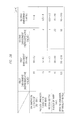
- FIG. 26 is a data diagram illustrating an example of respective values about a pad structure of a third embodiment.
- the third embodiment describes the size (representative value, range) of each part in the pad structure of the first embodiment, and the size (representative value, range) of each part in the pad structure of the second embodiment. That is, FIG. 26 indicates representative values and ranges of the pad structures of the first and second embodiments for each of a dimension of one side in a plan view of the via 4 h , a dimension of one side in a plan view of the recess 4 d , a depth of the recess 4 d , the radius r of the wire ball 5 a , and an opening dimension of one side in a plan view of the insulating film 4 i.
- connection failure between the wire ball 5 a and the electrode pad tends to occur when the depth of the recess 4 d is equal to or greater than 0.5 ⁇ m, for example. Accordingly, it can be said that the pad structure of the first embodiment and the pad structure of the second embodiment are effective when the depth of the recess 4 d is equal to or greater than 0.5 ⁇ m.
- FIG. 27 is an enlarged partial plan view illustrating a pad structure of a modification.
- This modification describes modifications such as the shape in a plan view of the via 4 h , and the number of vias 4 h disposed in one via disposition area 4 x . That is, in the first embodiment and the second embodiment, described has been a case where one via 4 h is disposed at one corner 4 n among four corners of the bonding pad 4 c , and a part or an entirety of the one via 4 h overlaps with the via disposition area 4 x .
- the plural vias (conductor connection portion) 4 h may be disposed at each of a plurality of (for example, four) corners 4 n .
- the via 4 h may be disposed at any two or three corners 4 n of four corners 4 n . Otherwise, the plural vias 4 h may be disposed only at one corner 4 n . That is, each of the number of corners 4 n at which the via 4 h is disposed, and the number of vias 4 h disposed in one corner 4 n may be one or plural.
- each of the via 4 h and the recess 4 d is not limited to a square, and may be a triangle or a polygon with five or more sides.
- the semiconductor device is not limited to the QFP 1 and may be another semiconductor device as far as it is a semiconductor device assembled by connecting the conductive wire to the electrode pad of the semiconductor chip.
Landscapes
- Engineering & Computer Science (AREA)
- Computer Hardware Design (AREA)
- Microelectronics & Electronic Packaging (AREA)
- Power Engineering (AREA)
- Physics & Mathematics (AREA)
- Internal Circuitry In Semiconductor Integrated Circuit Devices (AREA)
- Condensed Matter Physics & Semiconductors (AREA)
- General Physics & Mathematics (AREA)
- Wire Bonding (AREA)
- Geometry (AREA)
- Manufacturing & Machinery (AREA)
Abstract
A bonding pad of a semiconductor chip in a QFP includes, in its exposed portion, a via disposition area comprising: a first segment that connects a corner and a first point; a second segment that connects the corner and a second point; and an arc that connects the first point and the second point and forms a convex shape toward the corner. Further, in a plan view of the bonding pad, at least a part of a via is disposed so as to overlap with the via disposition area.
Description
The present application claims priority from. Japanese Patent Application No. 2016-126931 filed on Jun. 27, 2016 the content of which is hereby incorporated by reference into this application.
The present invention relates to a semiconductor device including an electrode pad to which a conductive wire is connected, for example.
With progress of miniaturization and cost reduction of semiconductor devices, miniaturization of a structure near electrode pads of semiconductor chips is also desired. Meanwhile, the number of electrode pads tends to increase due to multi-functionalization of the semiconductor devices.
In recent years, often used is a structure in which a lower layer wiring in a semiconductor chip and an electrode pad are electrically connected together through a via.
Incidentally, the structure in which the electrode pad of the semiconductor chip and the lower layer wiring are electrically connected through the via is disclosed in, for example, Japanese Patent Application Laid-open No. 2002-16069 (Patent Document 1) and Japanese Patent Application Laid-open No. 11-126790 (Patent Document 2).
As in the semiconductor device described above, in the structure in which the electrode pad and the lower layer wiring are electrically connected through the via, it is necessary to increase a via diameter in order to reduce resistance at a via portion. In addition, a recess (level difference, depression) is formed on the surface of the electrode pad on the via due to influence of coatability of sputter. If the wire bonding is performed on an area of the electrode pad on which the recess is formed, connection strength of wire bonding cannot be secured. As a countermeasure against this, therefore, it can be considered to draw out and dispose the via by using a lead wiring at a position outside an opening of an insulating film that defines the electrode pad.
However, since this structure brigs an increase in an area near the electrode pad, the miniaturization of the semiconductor chip cannot be achieved, and consequently the miniaturization of the semiconductor device cannot be achieved.
Other objects and novel characteristics of the present invention will be apparent from the description of the present specification and the accompanying drawings.
A semiconductor device according to one embodiment comprises: a semiconductor chip having an electrode pad; and a conductive wire including a wire connection portion electrically connected to the electrode pad. And, the semiconductor chip includes: a lower layer wiring formed in a lower layer of the electrode pad; a first insulating film that covers the lower layer wiring; a conductor connection portion that is disposed on the lower layer wiring, embedded in a first opening formed in the first insulating film, and is electrically connected to the lower layer wiring; and a second insulating film that covers a part of the electrode pad and on which a second opening that defines an exposed portion of the electrode pad is formed. Additionally, the electrode pad and the conductor connection portion are formed integrally. Additionally, the second opening includes: an intersection at which a first imaginary line along one side of two adjacent sides and a second imaginary line along the other side intersect each other; a first point on the first imaginary line positioned at a distance of a radius in a plan view of the wire connection portion from the intersection; and a second point on the second imaginary line positioned at the distance of the radius from the intersection. Further, the second opening includes a first area having: a first segment that connects the intersection and the first point; a second segment that connects the intersection and the second point; and an arc that connects the first point and the second point and forms a convex shape toward the intersection. Additionally, the wire connection portion is connected to a second area different from the first area in the second opening of the electrode pad, and at least a part of a recess formed in a surface of the electrode pad on the conductor connection portion overlaps with the first area in a plan view.
Additionally, another semiconductor device according to one embodiment comprises: a semiconductor chip having an electrode pad; and a conductive wire including a wire connection portion electrically connected to the electrode pad. And, the semiconductor chip includes: a lower layer wiring formed in a lower layer of the electrode pad; a first insulating film that covers the lower layer wiring; a conductor connection portion that is disposed on the lower layer wiring, embedded in a first opening formed in the first insulating film, and is electrically connected to the lower layer wiring; and
a second insulating film that covers a part of the electrode pad and on which a second opening that defines an exposed portion of the electrode pad is formed. Additionally, the electrode pad and the conductor connection portion are integrally formed. Then, the second opening includes: a first side and a second side that forma corner; a first point on the first side positioned at a distance of a radius in a plan view of the wire connection portion from the corner; and a second point on the second side positioned at the distance of the radius from the corner, and includes a first area having: a first segment that connects the corner and the first point; a second segment that connects the corner and the second point; and an arc that connects the first point and the second point and forms a convex shape toward the corner. Further, the wire connection portion is connected to a second area different from the first area in the second opening of the electrode pad, and at least a part of a recess formed on a surface of the electrode pad on the conductor connection portion overlaps with the first area in a plan view.
According to one embodiment described above, size reduction of the semiconductor chip can be achieved, and the miniaturization of the semiconductor device can be achieved.
The description of the same or similar portions is not repeated in principle unless particularly required in the following embodiments.
In the embodiments described below, the invention will be described in a plurality of sections or embodiments when required as a matter of convenience. However, these sections or embodiments are not irrelevant to each other unless otherwise stated, and the one relates to the entire or a part of the other as a modification example, details, or a supplementary explanation thereof.
Also, in the embodiments described below, when referring to the number of elements (including number of pieces, values, amount, range, and the like), the number of the elements is not limited to a specific number unless otherwise stated or except the case where the number is apparently limited to a specific number in principle, and the number larger or smaller than the specified number is also applicable.
Further, in the embodiments described below, it goes without saying that the components (including element steps) are not always indispensable unless otherwise stated or except the case where the components are apparently indispensable in principle.
Also, even when mentioning that constituent elements or the like are “made of A” or “made up of A” in the embodiments below, elements other than A are of course not excluded except the case where it is particularly specified that A is the only element thereof. Similarly, in the embodiments described below, when the shape of the components, positional relation thereof, and the like are mentioned, the substantially approximate and similar shapes and the like are included therein unless otherwise stated or except the case where it is conceivable that they are apparently excluded in principle. The same goes for the numerical value and the range described above.
Hereinafter, embodiments of the present invention will be described in detail with reference to the accompanying drawings. Incidentally, components having the same function are denoted by the same reference characters throughout the drawings for describing the embodiments, and the repetitive description thereof is omitted.
<Structure of Semiconductor Device>
The semiconductor device of the first embodiment illustrated in FIG. 1 is a semiconductor package assembled through wire bonding to an electrode pad of a semiconductor chip, and a quad flat package (QFP) 1 will be described as an example of the semiconductor device, in the first embodiment.
A configuration of the QFP 1 illustrated in FIGS. 1 and 2 , the QFP 1 is explained so as to include: a semiconductor chip 4 on which a semiconductor integrated circuit is formed; a plurality of inner leads 2 a radially disposed around the semiconductor chip 4; and a plurality of outer leads 2 b formed integrally with the respective inner leads 2 a. In addition, the QFP 1 includes: bonding pads 4 c that are electrode pads exposed on a principal surface 4 a of the semiconductor chip 4; and a plurality of wires (conductive wires) 5 that electrically connect the bonding pads 4 c and the respective inner leads 2 a corresponding to them.
Further, the QFP 1 includes: a tab (die pad) 2 c that is a chip mounting part fixed to the semiconductor chip 4 through a die bonding material 7 such as silver paste; and a sealing body 3 that is formed from a sealing resin etc. with resin molding and seals the semiconductor chip 4, the tab 2 c, the plurality of wires 5, and the plurality of inner leads 2 a. Since such a structure is a part of the QFP 1, the plurality of outer leads 2 b respectively formed integrally with the plurality of inner leads 2 a protrude externally from four sides of the sealing body 3, and each of the outer leads 2 b is bent and formed into a gull wing shape.
Here, the inner leads 2 a, the outer leads 2 b, and the tab 2 c are formed by a thin plate member of an iron-nickel alloy, a copper alloy, for example, and the sealing body 3 is made of a resin material such as a thermosetting epoxy resin and formed through resin molding.
In addition, the semiconductor chip 4 is formed of silicon etc., for example, and is fixed with the die bonding material 7 on the tab 2 c, and the semiconductor integrated circuit is formed on its principal surface 4 a. That is, a back surface 4 b of the semiconductor chip 4 and an upper surface of the tab 2 c are bonded through the die bonding material 7.
<Structure of Electrode Pad>
Described will be a basic structure of an electrode pad in the QFP 1 of the first embodiment with reference to FIGS. 3 and 4 . As illustrated in FIG. 3 , the semiconductor chip 4 includes the bonding pads 4 c that are the plural electrode pads exposed on the principal surface 4 a, and a wire 5 is connected to each of the bonding pads 4 c by thermocompression through wire bonding. That is, a wire ball (wire connection portion) 5 a having a tip of the wire 5 formed into a ball shape is electrically connected to the bonding pad 4 c.
In addition, in the semiconductor chip 4, a lower layer wiring 4 e is formed in a lower layer of the bonding pad 4 c, and the lower layer wiring 4 e is covered by an insulating film (first insulating film) 4 f disposed in the lower layer of the bonding pad 4 c.
In addition, formed on the lower layer wiring 4 e is a via (conductor connection portion) 4 h that is embedded in an opening (first opening) 4 g formed in the insulating film 4 f and is electrically connected to the lower layer wiring 4 e. Incidentally, the bonding pad 4 c and the via 4 h are integrally formed. That is, the bonding pad 4 c and the via 4 h are integrally formed by the same material.
In addition, a part of the bonding pad 4 c is covered by an insulating film (second insulating film) 4 i. In the insulating film 4 i, an opening (second opening) 4 j that defines an exposed portion 4 ca of the bonding pad 4 c is formed. That is, the exposed portion 4 ca of the bonding pad 4 c is defined, in a plan view, by a shape of the opening 4 j formed in the insulating film 4 i that covers the part of the bonding pad 4 c. In a case of the first embodiment, as illustrated in FIG. 4 , the opening 4 j of the insulating film 4 i forms a substantially square in a plan view, and the shape of the opening 4 j just corresponds to the shape of the exposed portion 4 ca of the bonding pad 4 c. Accordingly, the exposed portion 4 ca of the bonding pad 4 c and the opening 4 j of the insulating film 4 i have the same shape in a plan view, and this shape in the first embodiment is substantially square.
In addition, as illustrated in FIG. 3 , a recess 4 d (level difference, depression) is formed in a surface of the bonding pad 4 c on the via 4 h. When a conductor is embedded in the via opening 4 g in forming the conductor integrally with the bonding pad 4 c and the via 4 h by sputtering or the like, the recess 4 d is formed by a phenomenon (influence due to coatability of sputter) in which the upper surface of the bonding pad 4 c is recessed.
Next, description will be made for a wire ball disposition area (second area) 4 y in the exposed portion 4 ca of the bonding pad 4 c in the first embodiment illustrated in FIG. 4 and a via disposition area (first area, hatching area illustrated in FIG. 4 ) 4 x positioned outside the wire ball disposition area 4 y.
As illustrated in FIGS. 3 and 4 , the exposed portion 4 ca by the substantially square opening 4 j of the insulating film 4 i is formed on the bonding pad 4 c. The substantially square exposed portion 4 ca is divided into the wire ball disposition area 4 y, in which the wire ball 5 a can be disposed, and the via disposition area 4 x outside the wire ball disposition area 4 y. The via disposition area 4 x is positioned at each of four corners of the substantially square exposed portion 4 ca.
Here, a method for defining the via disposition area 4 x is explained so that the opening 4 j first includes an intersection 4 p at which a first imaginary line 4 s along a first side 4 k and a second imaginary line 4 t along a second side 4 m intersect each other. The first side 4 k is one side of two adjacent sides, and the second side 4 m is the other side thereof. Further, the opening 4 j includes a first point 4 q on the first imaginary line 4 s positioned at a distance of a radius r in a plan view of the wire ball 5 a from the intersection 4 p, and a second point 4 r on the second imaginary line 4 t positioned at a distance of the radius r from the intersection 4 p.
The via disposition area 4 x includes: a first segment 4 u that connects the intersection 4 p and the first point 4 q; a second segment 4 v that connects the intersection 4 p and the second point 4 r; and an arc 4 w that connects the first point 4 q and the second point 4 r and forms a convex shape toward the intersection 4 p. That is, the via disposition area 4 x formed at each of four corners of the substantially square exposed portion 4 ca is an area formed by the first segment 4 u having the distance r, the second segment 4 v having the same distance r, and the arc 4 w.
Meanwhile, the wire ball disposition area 4 y is an area other than the four (four corners) via disposition areas 4 x in the substantially square exposed portion 4 ca of the bonding pad 4 c, and is an area positioned inside each of the four via disposition areas 4 x. The wire 5 is connected to the wire ball disposition area 4 y different from the via disposition areas 4 x. That is, the wire ball 5 a is connected to the wire ball disposition area 4 y. At this time, the wire ball 5 a does not enter the via disposition area 4 x.
In the semiconductor device of the first embodiment, at least a part of the recess 4 d, which is formed on the via 4 h and is formed in the surface of the bonding pad 4 c, is formed in the via disposition area 4 x. That is, in a plan view, at least a part of the recess 4 d having a substantially square overlaps with the via disposition area 4 x.
In the pad structure illustrated in FIG. 4 , in a plan view, each part of the recess 4 d and the via 4 h each having a substantially square is formed across the via disposition area 4 x and an insulating film area 4 z in which the insulating film 4 i illustrated in FIG. 3 outside the exposed portion 4 ca (via disposition area 4 x) is formed. That is, the respective parts of the recess 4 d and the via 4 h overlap with both areas of the via disposition area 4 x and the insulating film area 4 z outside the via disposition area 4 x.
Next, in the pad structure illustrated in FIG. 4 , a method for defining the via disposition area 4 x will be described in a case where the exposed portion 4 ca of the bonding pad 4 c is square in a plan view and there are four corners 4 n in the exposed portion 4 ca.
In this case, the opening 4 j includes: the first side 4 k and the second side 4 m that form the corner 4 n; the first point 4 q on the first side 4 k positioned at the distance of the radius r in a plan view of the wire ball 5 a from the corner 4 n; and the second point 4 r on the second side 4 m positioned at the distance of the radius r from the corner 4 n.
Further, the opening 4 j includes: the via disposition area 4 x including the first segment 4 u that connects the corner 4 n and the first point 4 q; the second segment 4 v that connects the corner 4 n and the second point 4 r; and the arc 4 w that connects the first point 4 q and the second point 4 r and forms a convex shape toward the corner 4 n. That is, the opening 4 j has the four via disposition areas 4 x each including: the first segment 4 u having the length r from the corner 4 n; the second segment 4 v having the length r from the corner 4 n; and the arc 4 w.
In other words, the via disposition area 4 x is an area enclosed by: two sides (first side 4 k and second side 4 m) each extending from the corner 4 n of the opening 4 j to the length of the radius r of the wire ball 5 a; and the arc 4 w of the radius r of the wire ball 5 a having a convex shape toward the corner 4 n of the opening 4 j.
In a plan view, all or a part of a planar shape of the via 4 h is disposed in the via disposition area 4 x, and the wire ball 5 a is disposed in the wire ball disposition area 4 y different from the via disposition area 4 x. Therefore, the wire ball 5 a does not need to contact with the recess 4 d above the via 4 h, a lead wiring is omitted and the wire ball 5 a and the via 4 h can be electrically connected.
Thus, the pad structure is miniaturized, and miniaturization of the semiconductor chip 4 and miniaturization of the semiconductor device (QFP 1) can be achieved.
In addition, the recess 4 d formed right above the via 4 h makes it possible to relax a shock of a chip in a horizontal direction during the wire bonding by deforming a metal portion of the bonding pad 4 c in the horizontal direction.
As a result, by miniaturizing the semiconductor chip 4, connection reliability of the wire 5 to the bonding pad 4 c can be improved.
Next, described will be a specific example about the pad structure of the first embodiment using the basic structure of FIG. 3 . FIG. 5 is an enlarged partial cross-sectional view illustrating an example of a pad structure in the first embodiment; FIG. 6 is a plan view illustrating an example of the pad structure illustrated in FIG. 5 ; FIG. 7 is a plan view illustrating an example of the pad structure illustrated in FIG. 5 ; FIG. 8 is a plan view illustrating an example of a structure of an opening of a pad in the first embodiment; and FIG. 9 is a perspective view illustrating an example of the pad structure illustrated in FIG. 8 .
Here, described will be a structure of a case where a rewiring 4 cb is used as the bonding pad 4 c.
The pad structure illustrated in FIG. 5 is explained so that transistors 8 are formed on a Si substrate 9, and the transistors 8 and first wirings 10 are connected by contact parts 13. In addition, the first wirings 10 and the second wirings 11 are connected by first vias 14. Further, the second wirings 11 and third wirings 12 are connected by second vias 15. In addition, the third wiring 12 and the rewiring 4 cb are connected by the pad via (via 4 h).
Incidentally, the pad via (via 4 h) penetrates a moisture resistant insulating film 4 fa and a lower layer insulating film 4 fb. The pad via (via 4 h) is formed integrally with the rewiring 4 cb, and the recess 4 d (level difference, depression) is formed above the via 4 h.
Here, the rewiring 4 cb is formed by an electroplating method or an electroless plating method, is made of a material containing copper as a main component, for example, and is a wiring having a relatively greater thickness of about from 5 to 6 μm. In this case, the exposed portion 4 ca that is a part of the rewiring 4 cb becomes the bonding pad 4 c. In addition, since the rewiring 4 cb has the greater thickness, the via 4 h also has a relatively large size, and forms a square having a side of about 30 μm when its shape in a plan view is square.
In addition, the rewiring 4 cb is a wiring of the uppermost layer, and is formed on the lower layer insulating film 4 fb. Apart of the rewiring 4 cb is covered by the insulating film (second insulating film) 4 i that is an upper layer insulating film. The exposed portion 4 ca of the rewiring 4 cb is exposed from the opening 4 j of the insulating film 4 i, and the bonding pad 4 c to which the wire ball (wire connection portion) 5 a formed at a tip of the wire 5 is connected is formed on the exposed portion 4 ca. A part of an upper surface of the rewiring 4 cb is opened, and an adhesion layer 4 cc that improves adhesion properties with the wire 5 is formed on the surface of the bonding pad 4 c. In other words, the adhesion layer 4 cc is formed between the bonding pad 4 c configured by the rewiring 4 cb and the wire ball 5 a, and is a gold layer, a palladium layer, or a nickel layer, for example.
In addition, a barrier layer 4 cd may be formed between the rewiring 4 cb and the adhesion layer 4 cc, and a barrier layer 4 ce may be formed under the rewiring 4 cb. The barrier layer 4 cd is a nickel layer, for example, and the barrier layer 4 ce is a titanium layer, for example. That is, a structure and the number of the wiring layer configuring the rewiring 4 cb are not particularly limited, and the rewiring 4 cb may be formed by three kinds of metals, for example. Alternatively, the wire 5 may be connected directly to the surface of the rewiring 4 cb.
Incidentally, the wire 5 is made of a material containing copper as a main component, for example.
Next, described will be a size (an example) of each component in a case of using the rewiring 4 cb.
For example, when wire bonding is performed using the wire 5 with a radius of 20 μm, the radius r in a plan view of the wire ball (wire connection portion) 5 a is 40 μm.
The disposition area (via disposition area 4 x) of the pad via (via 4 h) is an area enclosed by: the first segment 4 u from the corner 4 n of the opening 4 j in the insulating film 4 i to the first point 4 q at 40 μm that is the same as the radius r of the wire ball 5 a on the first side 4 k; the second segment 4 v from the corner 4 n on the second side 4 m to the second point 4 r at the same distance; and the arc 4 w that connects the first point 4 q and the second point 4 r and has a concave shape toward the corner 4 n.
Here, described will be a method for calculating an overlapping length Y (see FIG. 8 ) with the via disposition area 4 x of the pad via in a case of the pad via (via 4 h) that is a square in a plan view.
As illustrated in FIGS. 8 and 9 , the radius of the wire ball 5 a is r, whereas the radius of the arc 4 w is also r. In this case, as illustrated in FIG. 8 , if it is assumed that a part of the via 4 h that enters the via disposition area 4 x is a square shape with a side length of Y (overlapping length), Y=r−r/√2=r×(1−1/√2)=0.29r. That is, the pad via (via 4 h) having about 0.29 times the radius r of the wire ball 5 a can be disposed (overlapped) inside (via disposition area 4 x). In the first embodiment, if it is assumed that the radius r of the wire ball 5 a is 40 μm, the pad via (via 4 h) can be disposed inside by 11.6 μm. That is, as illustrated in FIG. 6 , the pad via (via 4 h) can be overlapped with the via disposition area 4 x to a size of a square with a side (P) of 11.6 μm.
Incidentally, the pad via (via 4 h) is preferably disposed in the via disposition area (first area) 4 x, in a plan view. That is, the entirety of the pad via (via 4 h) with a square shape preferably falls within the via disposition area (first area) 4 x in a plan view.
In addition, in a case of the rewiring 4 cb as described in the first embodiment, it is necessary to set a distance T between an end of the rewiring 4 cb and the opening 4 j of the insulating film 4 i to 25 μm due to processing accuracy. That is, it is necessary to separate the end of the rewiring 4 cb from an edge of the opening 4 j in the insulating film 4 i by 25 μm. Here, a length K of one side of the opening 4 j is about 1.5 times the diameter of the wire ball 5 a. Accordingly, when the radius r of the wire ball 5 a is 40 μm, the length K of one side of the opening 4 j is 120 μm, and further the distance T between the end of the rewiring 4 cb and the opening 4 j in the insulating film 4 i is 25 μm, so that a size S of one side in a plan view of the rewiring 4 cb becomes 170 μm.
In addition, in referring to the size of the via 4 h (pad via) in a plan view (the length of one side of the square in a plan view) in the pad structure illustrated in FIG. 6 , the size is represented by a length from one upper end of the opening of the via 4 h (pad via) to the other upper end. For example, a size (length of one side) B of the via 4 h illustrated in FIG. 6 is 30 μm.
From the above, in the pad structure using the rewiring 4 cb illustrated in FIGS. 5 and 6 , the square via 4 h (pad via) with a side of 30 μm can be disposed without addition of the lead wiring.
Incidentally, due to the influence of positional accuracy at a time of the wire bonding, variation occurs in connection positions of the wire balls 5 a. FIG. 7 illustrates a case where the connection position of the wire ball 5 a varies in a direction toward the via 4 h. Even when the connection position of the wire ball 5 a varies in the direction toward the via 4 h as illustrated in FIG. 7 , a side wall of the opening 4 j in the insulating film 4 i inhibits the wire ball 5 a from entering toward the via direction, so that the wire ball 5 a does not enter into the via disposition area 4 x. That is, the wire ball 5 a can be prevented from being disposed on the recess 4 d.
<Method for Manufacturing Electrode Pad>
The method for manufacturing the electrode pad of the first embodiment will be described.
A structure in FIG. 10 illustrates a state in which the first wiring 10, the second wiring 11, and third wiring 12 have been formed, and then the moisture resistant insulating film 4 fa has been formed on the third wiring 12. An oxide film, TEOS, SiOC, an organic insulating film, or the like is suitable right above the third wiring 12. Silicon nitride having high moisture resistance is suitable for the uppermost surface, and its surface is a moisture resistant insulating film 4 fa.
Next, a structure in FIG. 11 illustrates a state in which the opening 4 g for the pad via (via 4 h) has been formed in the moisture resistant insulating film 4 fa. Here, a pattern is formed through a photolithography method using a photoresist, and then the opening 4 g for the pad via is formed in the third wiring 12 through an anisotropic dry etching method.
Next, a structure in FIG. 12 illustrates a state in which the lower layer insulating film 4 fb is applied onto the moisture resistant insulating film 4 fa. That is, the lower layer insulating film 4 fb is applied on an area from on the moisture resistant insulating film 4 fa to the opening 4 g. Thus, the lower layer insulating film 4 fb is formed on the moisture resistant insulating film 4 fa, and the lower layer insulating film 4 fb is embedded in the opening 4 g. At this time, photosensitive polyimide is suitable for the lower layer insulating film 4 fb.
Next, a structure in FIG. 13 illustrates a state in which the lower layer insulating film 4 fb has been pattern-formed through the photolithography method. Here, a desired area in the lower layer insulating film 4 fb is removed in order to form the opening 4 g for the pad via (via 4 h). At that time, the opening 4 g for the pad via (via 4 h) is formed by exposing and developing the lower layer insulating film 4 fb.
Next, a structure in FIG. 14 illustrates a state in which the barrier layer 4 ce of the rewiring 4 cb and a seed layer 4 cf for plating have been formed on the lower layer insulating film 4 fb so as to cover an entire surface of a wafer over. The seed layer 4 cf is a metal layer to which a current for plating is applied. Incidentally, it is suitable to form both of the barrier layer 4 ce and the seed layer 4 cf through a sputter method or a chemical vapor deposition (CVD) method.
Here, titanium, titanium nitride, tantalum, tantalum nitride, chromium, and a laminated film thereof, for example, are suitable for the barrier layer 4 ce of the rewiring 4 cb. Meanwhile, copper, palladium, gold, silver, platinum, iridium, ruthenium, rhodium, titanium, aluminum, manganese, nickel, and an alloy or a laminated film thereof, for example, are suitable for the seed layer 4 cf for plating.
Next, a structure in FIG. 15 illustrates a state in which a photoresist 4 cg has been applied onto the seed layer 4 cf, and a pattern of a rewiring layer has been formed through the photolithography method. Here, the photoresist 4 cg in an area that forms the rewiring 4 cb is selectively removed through the photolithography method, and is opened so that the seed layer 4 cf is exposed.
Next, a structure in FIG. 16 illustrates a state in which the rewiring 4 cb has been formed in the opening of the photoresist 4 cg. Copper, palladium, gold, silver, platinum, iridium, ruthenium, rhodium, titanium, aluminum, manganese, nickel, and an alloy or a laminated film thereof are suitable for metal configuring the rewiring 4 cb. In the pad structure illustrated in FIG. 5 , however, a case of using copper has been described as an example. Incidentally, an electroplating method, or an electroless plating method is suitable for forming the rewiring 4 cb.
Incidentally, at this time, a plating film does not completely fill on and above the pad via (via 4 h), and so the recess (level difference, depression) 4 d remains.
Next, a structure in FIG. 17 illustrates a state in which the photoresist 4 ch has been applied onto the rewiring 4 cb and the photoresist 4 cg of the rewiring 4 cb, and an opening for a bonding pad layer (adhesion layer) has been pattern-formed through the photolithography method. In this way, since the photoresist 4 cg of the rewiring 4 cb is left, the photoresist 4 ch can be uniformly applied and manufacturing cost can be reduced even when the photoresist 4 ch of the bonding pad layer has a small film thickness.
Next, a structure in FIG. 18 illustrates a state in which the barrier layer 4 cd and the adhesion layer 4 cc have been formed in an opening of the photoresist 4 ch. Incidentally, palladium, gold, silver, platinum, iridium, ruthenium, rhodium, titanium, and an alloy or a laminated film thereof, for example, are suitable for the adhesion layer 4 cc. In the pad structure illustrated in FIG. 5 , a case of using gold has been described as an example.
Meanwhile, nickel, titanium, tantalum, chromium, and an alloy or a laminated film thereof, for example, are suitable for the barrier layer 4 cd. In the pad structure illustrated in FIG. 5 , a case of using nickel has been described as an example. Incidentally, the barrier layer 4 cd is not necessarily formed. In addition, electroplating or electroless plating is suitable for forming the barrier layer 4 cd and the adhesion layer 4 cc.
Next, a structure in FIG. 19 illustrates a state in which the photoresists 4 cg and 4 ch of the rewiring 4 cb and the bonding pad layer have been removed. An organic acid, an organic solvent, or the like is suitable for removing the photoresists 4 cg and 4 ch. In this way, by leaving the photoresist 4 cg of the rewiring 4 cb, forming the photoresist 4 ch thereon, forming the barrier layer 4 cd and the adhesion layer 4 cc, and thereafter removing the photoresists 4 cg and 4 ch, the photoresists 4 cg and 4 ch can be removed at once and manufacturing cost can be reduced.
Next, a structure in FIG. 20 illustrates a state in which the seed layer 4 cf around the rewiring 4 cb has been removed. A mixed solution of sulfuric acid, hydrogen peroxide water, and water is suitable for removing the seed layer 4 cf, and the seed layer 4 cf is removed through wet etching by using the mixed solution. Thus, the seed layer 4 cf is removed, and the barrier layer 4 ce around the rewiring 4 cb is exposed.
Next, a structure in FIG. 21 illustrates a state in which the barrier layer 4 ce around the rewiring 4 cb has been removed. A mixed solution of ammonia, hydrogen peroxide water, and water is suitable for removing the barrier layer 4 ce around the rewiring 4 cb, and the barrier layer 4 ce is removed through wet etching by using the mixed solution. Thus, the barrier layer 4 ce is removed, the lower layer insulating film 4 fb is exposed, and as a result the rewiring 4 cb becomes formed.
Next, a structure in FIG. 22 illustrates a state in which the insulating film 4 i as the upper layer insulating film is applied onto the rewiring 4 cb, the lower layer insulating film 4 fb, and the moisture resistant insulating film 4 fa. At this time, photosensitive polyimide is suitable for the insulating film 4 i.
Next, a structure in FIG. 23 illustrates a state in which the insulating film 4 i has been pattern-formed through the photolithography method. That is, the insulating film 4 i over the bonding pad 4 c is removed. Here, the insulating film 4 i is removed by exposure and development, and then subjected to a heat treatment and polymerized. An opening of the bonding pad 4 c is set on the adhesion layer 4 cc.
From the above, formation of the bonding pad 4 c configured by the rewiring 4 cb is completed.
<Assembling of Semiconductor Device>
Assembly of the QFP 1 illustrated in FIGS. 1 and 2 will be described.
First, a die bonding process is performed. Here, the semiconductor chip 4 is mounted, through the die bonding material 7, on the tab 2 c of a lead frame not illustrated. At this time, the semiconductor chip 4 is mounted on the tab 2 c so that the principal surface 4 a from which the bonding pad 4 c of the semiconductor chip 4 is exposed faces upward.
Next, a wire bonding process is performed. The bonding pad 4 c of the semiconductor chip 4 and the inner lead 2 a of the lead frame are connected by the wire 5. At this time, on a semiconductor-chip side, the wire ball 5 a formed at the tip of the wire 5 is connected into the wire ball disposition area 4 y of the bonding pad 4 c.
Next, a resin sealing process is performed. Here, the sealing body 3 is formed so that the tab 2 c, the semiconductor chip 4, the inner leads, 2 a and the plurality of wires 5 are covered by using a resin for molding and that the outer leads 2 b are exposed.
Next, cutting and forming are performed. Here, the outer lead 2 b is cut and separated from a frame portion of the lead frame, and the outer lead 2 b is bent and formed into a gull wing shape. Thus, assembling of the QFP 1 is completed.
<Effects>
In a pad structure on an enlarged partial plan view of a comparative example illustrated in FIG. 28 and studied by the inventors, since there is the recess 4 d on the pad via (via 4 h) in the rewiring 4 cb that is the bonding pad 4 c, if the pad via (via 4 h) is disposed at a position of contacting (overlapping) with the wire ball 5 a illustrated in FIG. 5 , connection between the wire ball 5 a and the adhesion layer 4 cc becomes insufficient on the recess 4 d, and connection failure of the wire 5 is caused. Accordingly, it can be considered that the via 4 h is drawn out from and disposed outside the opening 4 j in the insulating film 4 i by using the lead wiring in order to prevent the connection failure of the wire 5 from being caused. In this case, however, the pad structure becomes large and, as a result, a chip area is expanded.
Therefore, in the QFP 1 of the first embodiment, by providing the insulating film 4 i that is the upper layer insulating film, the pad via (via 4 h) is disposed so that at least a part of the pad via (via 4 h) overlaps with the via disposition area 4 x formed by connecting: the corner 4 n of the opening 4 j in the insulating film 4 i; the first point 4 q at the same distance as the radius r of the wire ball 5 a from the corner 4 n; and the second point 4 r at the same distance as the radius r from the corner 4 n.
That is, in the exposed portion 4 ca of the bonding pad 4 c configured by the rewiring 4 cb, the pad via (via 4 h) is disposed so that at least a part of the pad via (via 4 h) overlaps with the via disposition area 4 x including: the first segment 4 u that connects the corner 4 n and the first point 4 q; the second segment 4 v that connects the corner 4 n and the second point 4 r; and the arc 4 w that connects the first point 4 q and the second point 4 r and forms a convex shape toward the corner 4 n. That is, in a plan view, at least a part of the pad via (via 4 h) is disposed so as to overlap with the via disposition area 4 x that is a part of the opening 4 j of the bonding pad 4 c, so that the lead wiring for drawing and disposing the via 4 h outside the opening 4 j is not used and reduction of the chip size can be achieved. As a result, miniaturization of the QFP 1 can be achieved.
In addition, reduction of the chip size can be achieved, so that cost reduction of the QFP 1 can be achieved.
Incidentally, the pad via (via 4 h) is preferably disposed in the via disposition area (first area) 4 x in a plan view. That is, the entire square pad via (via 4 h) in a plan view preferably falls within the via disposition area (first area) 4 x.
Thus, further reduction of the chip size can be achieved, and further miniaturization can be achieved in the size of the QFP 1.
In addition, even when the position of the wire ball 5 a shifts in a direction of the pad via (via 4 h), the wire ball 5 a is blocked by the side wall of the insulating film 4 i and cannot enter the pad via. As a result, in a plan view, the wire ball 5 a and the pad via (via 4 h) do not overlap each other, so that the connection failure in the wire bonding can be inhibited.
Thus, the connection reliability of the wire 5 in the QFP 1 can be improved.
Incidentally, at least a part in a plan view of the recess 4 d formed right above the via overlaps with the via disposition area 4 x, and so it can also be avoided that the recess 4 d and the wire ball 5 a overlap each other in a plan view.
In addition, the recess 4 d is formed in the surface of the bonding pad 4 c right above the via, so that a shock of a chip in a horizontal direction during the wire bonding can be absorbed by the recess 4 d. That is, the recess 4 d allows the metal portion of the bonding pad 4 c to deform in the horizontal direction, so that disconnection of the wire 5 can be inhibited and the connection reliability of the wire 5 can be improved.
Incidentally, when the wire 5 is made of a material containing copper as a main component, since copper is relatively hard, a phenomenon called a splash in which the metal portion of the bonding pad 4 c is pushed and scattered in the horizontal direction occurs in pressure-bonding the copper wire ball 5 a to the bonding pad 4 c, and the splash causes an electrical short circuit with the adjacent bonding pad 4 c.
However, in the pad structure of the first embodiment, as described above, since the recess 4 d is formed in the surface of the bonding pad 4 c right above the via, the metal portion of the bonding pad 4 c deforms in the horizontal direction, occurrence of the splash can be inhibited, and reduction of occurrence of electrical short circuit can be achieved.
In the second embodiment, described will be a case where the bonding pad 4 c in the pad structure is an Al pad 4 ci made of a material containing aluminum as a main component. Incidentally, in the second embodiment, described is a case of forming a 4-layer copper wiring using a dual damascene method in the lower layer wiring formed on the semiconductor chip 4. However, a type of the lower layer wiring and the number of its layers are not particularly limited.
The Al pad 4 ci is formed through sputtering or the like, and has a smaller thickness than the rewiring 4 cb of the first embodiment. Since the Al pad 4 ci has the smaller thickness, when the shape in a plan view of the via 4 h is square, the length of one side is about from 2 to 3 μm, which is smaller than 30 μm of the rewiring 4 cb.
As illustrated in FIG. 24 , a fourth wiring 16 and the Al pad 4 ci are connected by the pad via (via 4 h). The pad via (via 4 h) penetrates the lower layer insulating film 4 fb. Since the pad via (via 4 h) is formed integrally with the Al pad 4 ci made of a metal containing aluminum as a main component, there is the recess 4 d above the via. That is, since the Al pad 4 ci and the pad via (via 4 h) are integrally formed through one time sputtering, the recess 4 d is formed above the via.
In addition, a part of the bonding pad 4 c (Al pad 4 ci) is covered by the insulating film 4 i that is the upper layer insulating film, and further the wire ball 5 a is connected to the wire ball disposition area 4 y on the exposed portion 4 ca in the opening 4 j of the bonding pad 4 c.
In addition, the barrier layer 4 ce is formed on a lower surface of the Al pad 4 ci. Further, a barrier metal may exist also on an upper surface of the Al pad 4 ci, but the barrier metal is removed from the opening 4 j in the insulating film 4 i that is the upper layer insulating film, and thereby the exposed portion 4 ca is exposed.
Incidentally, an adhesion metal, or a laminated film of the adhesion metal and the barrier metal may be formed on the upper surface of the Al pad 4 ci. The adhesion metal is, for example, palladium, or gold. The barrier metal is, for example, titanium, titanium nitride, chromium, tantalum, or tantalum nitride.
In addition, in the pad structure of the second embodiment, the adhesion insulating film 4 cj is formed on the insulating film 4 i that is the upper layer insulating film. The adhesion insulating film 4 cj is one for improving adhesion with a resin (sealing resin) contained in a packaging material of the semiconductor device, and the opening of the adhesion insulating film 4 cj is positioned outside the opening 4 j of the insulating film 4 i. As the adhesion insulating film 4 cj, polyimide is suitable.
Similarly to the pad structure of the first embodiment also in the pad structure of the second embodiment, as illustrated in FIG. 25 , the pad via (via 4 h) is disposed so that at least a part of the pad via (via 4 h) overlaps with the via disposition area 4 x formed by connecting: the corner 4 n of the opening 4 j in the insulating film 4 i; the first point 4 q at the same distance as the radius r of the wire ball 5 a from the corner 4 n; and the second point 4 r at the same distance as the radius r from the corner 4 n.
That is, in the exposed portion 4 ca of the bonding pad 4 c configured by the Al pad 4 ci, the pad via (via 4 h) is disposed so that at least a part of the pad via (via 4 h) overlaps with the via disposition area 4 x including: the first segment 4 u that connects the corner 4 n and the first point 4 q; the second segment 4 v that connects the corner 4 n and the second point 4 r; and the arc 4 w that connects the first point 4 q and the second point 4 r and forms a convex shape towards the corner 4 n.
In addition, similarly to the first embodiment, at least a part in a plan view of the recess 4 d formed right above the via overlaps with the via disposition area 4 x, and so it can be avoided that the recess 4 d and the wire ball 5 a overlap each other in a plan view.
Next, described will be an example about a size of each part of the pad structure of the second embodiment illustrated in FIG. 25 . A distance T between the end of the Al pad 4 ci and the opening 4 j in the insulating film 4 i has to be secured at about 2.5 μm. In addition, the length K of one side of the opening 4 j is 55 μm, and further the distance T between the end of the Al pad 4 ci and the opening 4 j in the insulating film 4 i is 2.5 μm, so that a size S of one side in a plan view of the Al pad 4 ci becomes 60 μm.
In addition, a size (length of one side) B of the via 4 h is about 3 μm.
From the above, also in the pad structure using the Al pad 4 ci of the second embodiment, the square via 4 h (pad via) with a side of 3 μm can be disposed without addition of the lead wiring.
Incidentally, similarly to the first embodiment, if it is assumed that a part of the via 4 h entering the via disposition area 4 x is a square with a side length of Y (overlapping length), Y=r−r/√2=r×(1−1/√2)=0.29r, and the pad via (via 4 h) with about 0.29 times the radius r of the wire ball 5 a can be disposed (overlapped) inside (in the via disposition area 4 x). In the second embodiment, if it is assumed that the radius r of the wire ball 5 a is 20 μm, the pad via (via 4 h) can be disposed inside by 5.8 μm. That is, the pad via (via 4 h) can be overlapped with the via disposition area 4 x by a size of a square with a side (P) of 5.8 μm.
In addition, since the side wall of the adhesion insulating film 4 cj blocks entering of the wire ball 5 a even when the adhesion insulating film 4 cj is inside from the insulating film 4 i that is the upper layer insulating film, the wire ball 5 a is blocked by the side wall of the adhesion insulating film 4 cj and cannot enter the pad via when the position of the wire ball 5 a deviates in the direction of the pad via (via 4 h). As a result, in a plan view, the wire ball 5 a and the pad via (via 4 h) do not overlap each other, so that the connection failure in the wire bonding can be inhibited.
According to the semiconductor device of the second embodiment, the pad via (via 4 h) is disposed so that at least a part of the pad via (via 4 h) overlaps with the via disposition area 4 x in the exposed portion 4 ca of the Al pad 4 ci, and so the pad via (via 4 h) can be disposed without use of the lead wiring.
Thus, reduction of the chip size can be achieved, and miniaturization of the semiconductor device (QFP 1) can be achieved.
In addition, reduction of the chip size can be achieved, so that cost reduction of the semiconductor device (QFP 1) can be achieved.
Since other effects obtained by the semiconductor device of the second embodiment are similar to those of the first embodiment, duplicate descriptions thereof are omitted.
From FIG. 26 , it can be seen that the connection failure between the wire ball 5 a and the electrode pad tends to occur when the depth of the recess 4 d is equal to or greater than 0.5 μm, for example. Accordingly, it can be said that the pad structure of the first embodiment and the pad structure of the second embodiment are effective when the depth of the recess 4 d is equal to or greater than 0.5 μm.
<Modification>
This modification describes modifications such as the shape in a plan view of the via 4 h, and the number of vias 4 h disposed in one via disposition area 4 x. That is, in the first embodiment and the second embodiment, described has been a case where one via 4 h is disposed at one corner 4 n among four corners of the bonding pad 4 c, and a part or an entirety of the one via 4 h overlaps with the via disposition area 4 x. However, for example, as illustrated in FIG. 27 , the plural vias (conductor connection portion) 4 h may be disposed at each of a plurality of (for example, four) corners 4 n. Alternatively, the via 4 h may be disposed at any two or three corners 4 n of four corners 4 n. Otherwise, the plural vias 4 h may be disposed only at one corner 4 n. That is, each of the number of corners 4 n at which the via 4 h is disposed, and the number of vias 4 h disposed in one corner 4 n may be one or plural.
In addition, the shape in a plan view of each of the via 4 h and the recess 4 d is not limited to a square, and may be a triangle or a polygon with five or more sides.
Although the invention made by the present inventors has been described specifically based on the embodiments above, the present invention is not limited to the embodiments described above, and it goes without saying that various modifications can be made without departing from the gist thereof.
In the first and second embodiments, although the case where the semiconductor device is the QFP 1 has been described, the semiconductor device is not limited to the QFP 1 and may be another semiconductor device as far as it is a semiconductor device assembled by connecting the conductive wire to the electrode pad of the semiconductor chip.
Claims (19)
1. A semiconductor device, comprising:
a semiconductor chip including an electrode pad; and
a conductive wire including a wire connection portion electrically connected to the electrode pad,
wherein the semiconductor chip includes:
a lower layer wiring formed in a lower layer of the electrode pad;
a first insulating film that covers the lower layer wiring;
a conductor connection portion that is disposed on the lower layer wiring, embedded in a first opening formed in the first insulating film, and is electrically connected to the lower layer wiring; and
a second insulating film that covers a part of the electrode pad and on which a second opening that defines an exposed portion of the electrode pad is formed,
wherein the electrode pad and the conductor connection portion are integrally formed,
wherein the second opening includes:
an intersection at which a first imaginary line along one side of two adjacent sides and a second imaginary line along an other side intersect each other,
a first point on the first imaginary line positioned at a distance of a radius in a plan view of the wire connection portion from the intersection; and
a second point on the second imaginary line positioned at the distance of the radius from the intersection, and includes a first area including:
a first segment that connects the intersection and the first point;
a second segment that connects the intersection and the second point; and
an arc that connects the first point and the second point and forms a convex shape toward the intersection,
wherein the wire connection portion is connected to a second area, different from the first area, in the second opening of the electrode pad,
wherein at least a part of a recess formed in a surface of the electrode pad on the conductor connection portion overlaps with the first area in the plan view, and
wherein, in the plan view, at least a part of the wire connection portion of the conductive wire is located in a region different from the lower layer wiring.
2. The semiconductor device according to claim 1 , wherein the conductor connection portion is disposed, in the plan view, across the first area and an insulating film area on which the second insulating film is formed outside the first area.
3. The semiconductor device according to claim 1 , wherein the conductor connection portion is disposed in the first area in the plan view.
4. The semiconductor device according to claim 1 , wherein the conductive wire comprises a material containing copper as a main component.
5. The semiconductor device according to claim 1 , wherein the electrode pad comprises a material containing copper as a main component.
6. The semiconductor device according to claim 1 , wherein the electrode pad comprises a material containing aluminum as a main component.
7. The semiconductor device according to claim 1 , wherein at least one alloy layer of a palladium layer, a gold layer, and a nickel layer is disposed between the electrode pad and the wire connection portion.
8. The semiconductor device according to claim 1 , wherein a depth of the recess is equal to or greater than 0.5 μm.
9. The semiconductor device according to claim 1 , wherein, in the plan view, the first opening overlaps with the second opening.
10. The semiconductor device according to claim 1 , wherein the second insulating film is disposed on a surface of the first insulating film.
11. The semiconductor device according to claim 1 , wherein, in the plan view, the recess is located in the second opening.
12. The semiconductor device according to claim 1 , wherein, in the plan view, an entirety of the recess is located outside of the wire connection portion of the conductive wire.
13. A semiconductor device, comprising:
a semiconductor chip including an electrode pad; and
a conductive wire including a wire connection portion electrically connected to the electrode pad,
wherein the semiconductor chip includes:
a lower layer wiring formed in a lower layer of the electrode pad;
a first insulating film that covers the lower layer wiring;
a conductor connection portion that is disposed on the lower layer wiring, embedded in a first opening formed in the first insulating film, and is electrically connected to the lower layer wiring; and
a second insulating film that covers a part of the electrode pad and on which a second opening that defines an exposed portion of the electrode pad is formed,
wherein the electrode pad and the conductor connection portion are integrally formed,
wherein the second opening includes:
a first side and a second side that form a corner;
a first point on the first side positioned at a distance of a radius in a plan view of the wire connection portion from the corner; and
a second point on the second side positioned at the distance of the radius from the corner, and includes a first area including:
a first segment that connects the corner and the first point;
a second segment that connects the corner and the second point; and
an are that connects the first point and the second point and forms a convex shape toward the corner,
wherein the wire connection portion is connected to a second area, different from the first area, in the second opening of the electrode pad,
wherein at least a part of a recess formed on a surface of the electrode pad on the conductor connection portion overlaps with the first area in the plan view; and
wherein, in the plan view, at least a part of the wire connection portion of the conductive wire is located in a region different from the lower layer wiring.
14. The semiconductor device according to claim 13 , wherein the conductor connection portion is disposed, in the plan view, across the first area and an insulating film area on which the second insulating film is formed outside the first area.
15. The semiconductor device according to claim 13 , wherein the conductor connection portion is disposed in the first area in the plan view.
16. The semiconductor device according to claim 13 , wherein the electrode pad comprises a material containing copper as a main component.
17. The semiconductor device according to claim 13 , wherein the electrode pad comprises a material containing aluminum as a main component.
18. The semiconductor device according to claim 13 , wherein each of the corner and the conductor connection portion is one or plural in number, the conductor connection portion is disposed at the one corner or each of the plural corner.
19. The semiconductor device according to claim 13 , wherein a depth of the recess is equal to or greater than 0.5 μm.
Applications Claiming Priority (2)
| Application Number | Priority Date | Filing Date | Title |
|---|---|---|---|
| JP2016126931A JP6649189B2 (en) | 2016-06-27 | 2016-06-27 | Semiconductor device |
| JP2016-126931 | 2016-06-27 |
Publications (2)
| Publication Number | Publication Date |
|---|---|
| US20170372996A1 US20170372996A1 (en) | 2017-12-28 |
| US10204853B2 true US10204853B2 (en) | 2019-02-12 |
Family
ID=59227586
Family Applications (1)
| Application Number | Title | Priority Date | Filing Date |
|---|---|---|---|
| US15/621,745 Active US10204853B2 (en) | 2016-06-27 | 2017-06-13 | Semiconductor device |
Country Status (6)
| Country | Link |
|---|---|
| US (1) | US10204853B2 (en) |
| EP (1) | EP3264453A1 (en) |
| JP (1) | JP6649189B2 (en) |
| KR (1) | KR20180001444A (en) |
| CN (2) | CN207542239U (en) |
| TW (1) | TW201802946A (en) |
Cited By (1)
| Publication number | Priority date | Publication date | Assignee | Title |
|---|---|---|---|---|
| US20190279922A1 (en) * | 2018-03-09 | 2019-09-12 | Infineon Technologies Ag | Semiconductor Device Including Bonding Pad and Bond Wire or Clip |
Families Citing this family (8)
| Publication number | Priority date | Publication date | Assignee | Title |
|---|---|---|---|---|
| CN108231723B (en) * | 2016-12-22 | 2020-08-07 | 中芯国际集成电路制造(上海)有限公司 | Package structure and method of forming the same |
| DE112019006263T5 (en) | 2018-12-18 | 2021-09-09 | Rohm Co., Ltd. | SEMICONDUCTOR COMPONENTS AND MANUFACTURING METHOD FOR SEMICONDUCTOR COMPONENTS |
| US10804176B2 (en) * | 2019-02-21 | 2020-10-13 | Win Semiconductors Corp. | Low stress moisture resistant structure of semiconductor device |
| JP7339000B2 (en) * | 2019-03-18 | 2023-09-05 | ローム株式会社 | Semiconductor equipment and semiconductor packages |
| US11270962B2 (en) | 2019-10-28 | 2022-03-08 | Nanya Technology Corporation | Semiconductor device and method of manufacturing the same |
| US11538777B2 (en) * | 2020-07-01 | 2022-12-27 | Sandisk Technologies Llc | Semiconductor structure containing pre-polymerized protective layer and method of making thereof |
| US11776922B2 (en) * | 2020-07-01 | 2023-10-03 | Sandisk Technologies Llc | Semiconductor structure containing pre-polymerized protective layer and method of making thereof |
| CN113345862B (en) * | 2021-04-09 | 2026-01-23 | 日月光半导体制造股份有限公司 | Nail frame structure and semiconductor structure |
Citations (11)
| Publication number | Priority date | Publication date | Assignee | Title |
|---|---|---|---|---|
| US5736791A (en) | 1995-02-07 | 1998-04-07 | Mitsubishi Denki Kabushiki Kaisha | Semiconductor device and bonding pad structure therefor |
| JPH11126790A (en) | 1997-08-21 | 1999-05-11 | Seiko Epson Corp | Semiconductor device |
| JP2002016069A (en) | 2000-06-29 | 2002-01-18 | Matsushita Electric Ind Co Ltd | Semiconductor device and method of manufacturing the same |
| US20050001324A1 (en) | 2003-07-01 | 2005-01-06 | Motorola, Inc. | Corrosion-resistant copper bond pad and integrated device |
| US20080217786A1 (en) * | 2007-01-31 | 2008-09-11 | Renesas Technology Corp. | Semiconductor device and method of manufacturing semiconductor device |
| JP2010050177A (en) | 2008-08-20 | 2010-03-04 | Sharp Corp | Semiconductor device |
| US20110024744A1 (en) | 2009-07-31 | 2011-02-03 | E2V Semiconductors | Connection pad structure for an electronic component |
| US20130062742A1 (en) | 2011-09-12 | 2013-03-14 | Conexant Systems, Inc. | Spot Plated Leadframe and IC Bond Pad Via Array Design for Copper Wire |
| US20150115269A1 (en) | 2013-10-30 | 2015-04-30 | Renesas Electronics Corporation | Semiconductor Device and Method for Manufacturing Semiconductor Device |
| US20150333010A1 (en) * | 2014-05-15 | 2015-11-19 | Texas Instruments Incorporated | Bond pad having ruthenium directly on passivation sidewall |
| US20160163666A1 (en) * | 2014-12-04 | 2016-06-09 | Renesas Electronics Corporation | Semiconductor device and manufacturing method for the same |
Family Cites Families (10)
| Publication number | Priority date | Publication date | Assignee | Title |
|---|---|---|---|---|
| US6765277B2 (en) * | 2002-01-15 | 2004-07-20 | Taiwan Semiconductor Manufacturing Co., Ltd. | Microelectronic fabrication with corrosion inhibited bond pad |
| JP2005064218A (en) * | 2003-08-12 | 2005-03-10 | Renesas Technology Corp | Semiconductor device |
| JP4951276B2 (en) * | 2006-05-29 | 2012-06-13 | ルネサスエレクトロニクス株式会社 | Semiconductor chip and semiconductor device |
| US7652379B2 (en) * | 2007-07-23 | 2010-01-26 | National Semiconductor Corporation | Bond pad stacks for ESD under pad and active under pad bonding |
| JP2010147267A (en) * | 2008-12-19 | 2010-07-01 | Renesas Technology Corp | Semiconductor integrated circuit device and method of manufacturing the same |
| JP5353313B2 (en) * | 2009-03-06 | 2013-11-27 | 富士通セミコンダクター株式会社 | Semiconductor device |
| JP2011003578A (en) * | 2009-06-16 | 2011-01-06 | Renesas Electronics Corp | Semiconductor device |
| JP2012186366A (en) * | 2011-03-07 | 2012-09-27 | Panasonic Corp | Semiconductor device and manufacturing method of the same |
| JP5919128B2 (en) * | 2012-08-03 | 2016-05-18 | ルネサスエレクトロニクス株式会社 | Semiconductor device and manufacturing method thereof |
| JP2015142009A (en) * | 2014-01-29 | 2015-08-03 | サンケン電気株式会社 | Semiconductor device |
-
2016
- 2016-06-27 JP JP2016126931A patent/JP6649189B2/en active Active
-
2017
- 2017-05-29 KR KR1020170066102A patent/KR20180001444A/en not_active Withdrawn
- 2017-06-13 US US15/621,745 patent/US10204853B2/en active Active
- 2017-06-15 TW TW106119900A patent/TW201802946A/en unknown
- 2017-06-21 CN CN201720726572.7U patent/CN207542239U/en not_active Expired - Fee Related
- 2017-06-21 CN CN201710475947.1A patent/CN107546206B/en active Active
- 2017-06-26 EP EP17177976.2A patent/EP3264453A1/en not_active Withdrawn
Patent Citations (11)
| Publication number | Priority date | Publication date | Assignee | Title |
|---|---|---|---|---|
| US5736791A (en) | 1995-02-07 | 1998-04-07 | Mitsubishi Denki Kabushiki Kaisha | Semiconductor device and bonding pad structure therefor |
| JPH11126790A (en) | 1997-08-21 | 1999-05-11 | Seiko Epson Corp | Semiconductor device |
| JP2002016069A (en) | 2000-06-29 | 2002-01-18 | Matsushita Electric Ind Co Ltd | Semiconductor device and method of manufacturing the same |
| US20050001324A1 (en) | 2003-07-01 | 2005-01-06 | Motorola, Inc. | Corrosion-resistant copper bond pad and integrated device |
| US20080217786A1 (en) * | 2007-01-31 | 2008-09-11 | Renesas Technology Corp. | Semiconductor device and method of manufacturing semiconductor device |
| JP2010050177A (en) | 2008-08-20 | 2010-03-04 | Sharp Corp | Semiconductor device |
| US20110024744A1 (en) | 2009-07-31 | 2011-02-03 | E2V Semiconductors | Connection pad structure for an electronic component |
| US20130062742A1 (en) | 2011-09-12 | 2013-03-14 | Conexant Systems, Inc. | Spot Plated Leadframe and IC Bond Pad Via Array Design for Copper Wire |
| US20150115269A1 (en) | 2013-10-30 | 2015-04-30 | Renesas Electronics Corporation | Semiconductor Device and Method for Manufacturing Semiconductor Device |
| US20150333010A1 (en) * | 2014-05-15 | 2015-11-19 | Texas Instruments Incorporated | Bond pad having ruthenium directly on passivation sidewall |
| US20160163666A1 (en) * | 2014-12-04 | 2016-06-09 | Renesas Electronics Corporation | Semiconductor device and manufacturing method for the same |
Non-Patent Citations (1)
| Title |
|---|
| Extended European Search Report dated Nov. 24, 2017 in European Application No. 17177976.2. |
Cited By (3)
| Publication number | Priority date | Publication date | Assignee | Title |
|---|---|---|---|---|
| US20190279922A1 (en) * | 2018-03-09 | 2019-09-12 | Infineon Technologies Ag | Semiconductor Device Including Bonding Pad and Bond Wire or Clip |
| US10971435B2 (en) * | 2018-03-09 | 2021-04-06 | Infineon Technologies Ag | Semiconductor device including bonding pad and bond wire or clip |
| US11837528B2 (en) | 2018-03-09 | 2023-12-05 | Infineon Technologies Ag | Method of manufacturing a semiconductor device having a bond wire or clip bonded to a bonding pad |
Also Published As
| Publication number | Publication date |
|---|---|
| CN107546206A (en) | 2018-01-05 |
| TW201802946A (en) | 2018-01-16 |
| EP3264453A1 (en) | 2018-01-03 |
| CN207542239U (en) | 2018-06-26 |
| CN107546206B (en) | 2022-10-14 |
| US20170372996A1 (en) | 2017-12-28 |
| KR20180001444A (en) | 2018-01-04 |
| JP2018006385A (en) | 2018-01-11 |
| JP6649189B2 (en) | 2020-02-19 |
Similar Documents
| Publication | Publication Date | Title |
|---|---|---|
| US10204853B2 (en) | Semiconductor device | |
| US12009350B2 (en) | Semiconductor package and method of fabricating the same | |
| US12243813B2 (en) | Connection structure and method of forming the same | |
| US10818601B1 (en) | Semiconductor device and method of manufacturing the same | |
| US20050224962A1 (en) | Manufacturing method for semiconductor integrated circuit, semiconductor integrated circuit, and semiconductor integrated circuit apparatus | |
| US8361857B2 (en) | Semiconductor device having a simplified stack and method for manufacturing thereof | |
| CN101128926A (en) | Structure and method for manufacturing flip chip device | |
| JP4775007B2 (en) | Semiconductor device and manufacturing method thereof | |
| CN108511410B (en) | Semiconductor devices | |
| CN114551415A (en) | Semiconductor package | |
| JP6577899B2 (en) | Manufacturing method of semiconductor device | |
| US20070013064A1 (en) | Semiconductor device and electronic apparatus | |
| US7479706B2 (en) | Chip package structure | |
| US11769737B2 (en) | Semiconductor package | |
| US12284758B2 (en) | Printed circuit board | |
| US20170317031A1 (en) | Fabrication Method OF A Package Substrate | |
| US20240429151A1 (en) | Semiconductor package and method of manufacturing semiconductor package | |
| JP2020061580A (en) | Semiconductor device | |
| JP2007115984A (en) | Semiconductor device and manufacturing method thereof |
Legal Events
| Date | Code | Title | Description |
|---|---|---|---|
| AS | Assignment |
Owner name: RENESAS ELECTRONICS CORPORATION, JAPAN Free format text: ASSIGNMENT OF ASSIGNORS INTEREST;ASSIGNORS:MATSUMOTO, MASAHIRO;YAJIMA, AKIRA;MAEKAWA, KAZUYOSHI;SIGNING DATES FROM 20170511 TO 20171013;REEL/FRAME:043906/0584 |
|
| STCF | Information on status: patent grant |
Free format text: PATENTED CASE |
|
| MAFP | Maintenance fee payment |
Free format text: PAYMENT OF MAINTENANCE FEE, 4TH YEAR, LARGE ENTITY (ORIGINAL EVENT CODE: M1551); ENTITY STATUS OF PATENT OWNER: LARGE ENTITY Year of fee payment: 4 |