US10199492B2 - Folded channel trench MOSFET - Google Patents
Folded channel trench MOSFET Download PDFInfo
- Publication number
- US10199492B2 US10199492B2 US15/364,827 US201615364827A US10199492B2 US 10199492 B2 US10199492 B2 US 10199492B2 US 201615364827 A US201615364827 A US 201615364827A US 10199492 B2 US10199492 B2 US 10199492B2
- Authority
- US
- United States
- Prior art keywords
- layer
- channel
- epitaxial layer
- conductivity type
- channel width
- Prior art date
- Legal status (The legal status is an assumption and is not a legal conclusion. Google has not performed a legal analysis and makes no representation as to the accuracy of the status listed.)
- Active, expires
Links
Images


Classifications
-
- H01L29/7813—
-
- H—ELECTRICITY
- H10—SEMICONDUCTOR DEVICES; ELECTRIC SOLID-STATE DEVICES NOT OTHERWISE PROVIDED FOR
- H10D—INORGANIC ELECTRIC SEMICONDUCTOR DEVICES
- H10D30/00—Field-effect transistors [FET]
- H10D30/60—Insulated-gate field-effect transistors [IGFET]
- H10D30/64—Double-diffused metal-oxide semiconductor [DMOS] FETs
- H10D30/66—Vertical DMOS [VDMOS] FETs
- H10D30/668—Vertical DMOS [VDMOS] FETs having trench gate electrodes, e.g. UMOS transistors
-
- H—ELECTRICITY
- H10—SEMICONDUCTOR DEVICES; ELECTRIC SOLID-STATE DEVICES NOT OTHERWISE PROVIDED FOR
- H10D—INORGANIC ELECTRIC SEMICONDUCTOR DEVICES
- H10D30/00—Field-effect transistors [FET]
- H10D30/60—Insulated-gate field-effect transistors [IGFET]
- H10D30/62—Fin field-effect transistors [FinFET]
-
- H—ELECTRICITY
- H01—ELECTRIC ELEMENTS
- H01L—SEMICONDUCTOR DEVICES NOT COVERED BY CLASS H10
- H01L21/00—Processes or apparatus adapted for the manufacture or treatment of semiconductor or solid state devices or of parts thereof
- H01L21/02—Manufacture or treatment of semiconductor devices or of parts thereof
- H01L21/04—Manufacture or treatment of semiconductor devices or of parts thereof the devices having potential barriers, e.g. a PN junction, depletion layer or carrier concentration layer
- H01L21/18—Manufacture or treatment of semiconductor devices or of parts thereof the devices having potential barriers, e.g. a PN junction, depletion layer or carrier concentration layer the devices having semiconductor bodies comprising elements of Group IV of the Periodic Table or AIIIBV compounds with or without impurities, e.g. doping materials
- H01L21/26—Bombardment with radiation
- H01L21/263—Bombardment with radiation with high-energy radiation
- H01L21/265—Bombardment with radiation with high-energy radiation producing ion implantation
- H01L21/266—Bombardment with radiation with high-energy radiation producing ion implantation using masks
-
- H—ELECTRICITY
- H01—ELECTRIC ELEMENTS
- H01L—SEMICONDUCTOR DEVICES NOT COVERED BY CLASS H10
- H01L21/00—Processes or apparatus adapted for the manufacture or treatment of semiconductor or solid state devices or of parts thereof
- H01L21/70—Manufacture or treatment of devices consisting of a plurality of solid state components formed in or on a common substrate or of parts thereof; Manufacture of integrated circuit devices or of parts thereof
- H01L21/71—Manufacture of specific parts of devices defined in group H01L21/70
- H01L21/768—Applying interconnections to be used for carrying current between separate components within a device comprising conductors and dielectrics
- H01L21/76838—Applying interconnections to be used for carrying current between separate components within a device comprising conductors and dielectrics characterised by the formation and the after-treatment of the conductors
- H01L21/76877—Filling of holes, grooves or trenches, e.g. vias, with conductive material
- H01L21/76883—Post-treatment or after-treatment of the conductive material
-
- H—ELECTRICITY
- H01—ELECTRIC ELEMENTS
- H01L—SEMICONDUCTOR DEVICES NOT COVERED BY CLASS H10
- H01L21/00—Processes or apparatus adapted for the manufacture or treatment of semiconductor or solid state devices or of parts thereof
- H01L21/70—Manufacture or treatment of devices consisting of a plurality of solid state components formed in or on a common substrate or of parts thereof; Manufacture of integrated circuit devices or of parts thereof
- H01L21/71—Manufacture of specific parts of devices defined in group H01L21/70
- H01L21/768—Applying interconnections to be used for carrying current between separate components within a device comprising conductors and dielectrics
- H01L21/76897—Formation of self-aligned vias or contact plugs, i.e. involving a lithographically uncritical step
-
- H—ELECTRICITY
- H01—ELECTRIC ELEMENTS
- H01L—SEMICONDUCTOR DEVICES NOT COVERED BY CLASS H10
- H01L23/00—Details of semiconductor or other solid state devices
- H01L23/52—Arrangements for conducting electric current within the device in operation from one component to another, i.e. interconnections, e.g. wires, lead frames
- H01L23/522—Arrangements for conducting electric current within the device in operation from one component to another, i.e. interconnections, e.g. wires, lead frames including external interconnections consisting of a multilayer structure of conductive and insulating layers inseparably formed on the semiconductor body
- H01L23/528—Layout of the interconnection structure
- H01L23/5283—Cross-sectional geometry
-
- H01L29/0865—
-
- H01L29/1095—
-
- H01L29/66734—
-
- H—ELECTRICITY
- H10—SEMICONDUCTOR DEVICES; ELECTRIC SOLID-STATE DEVICES NOT OTHERWISE PROVIDED FOR
- H10D—INORGANIC ELECTRIC SEMICONDUCTOR DEVICES
- H10D30/00—Field-effect transistors [FET]
- H10D30/01—Manufacture or treatment
- H10D30/021—Manufacture or treatment of FETs having insulated gates [IGFET]
- H10D30/024—Manufacture or treatment of FETs having insulated gates [IGFET] of fin field-effect transistors [FinFET]
-
- H—ELECTRICITY
- H10—SEMICONDUCTOR DEVICES; ELECTRIC SOLID-STATE DEVICES NOT OTHERWISE PROVIDED FOR
- H10D—INORGANIC ELECTRIC SEMICONDUCTOR DEVICES
- H10D30/00—Field-effect transistors [FET]
- H10D30/01—Manufacture or treatment
- H10D30/021—Manufacture or treatment of FETs having insulated gates [IGFET]
- H10D30/028—Manufacture or treatment of FETs having insulated gates [IGFET] of double-diffused metal oxide semiconductor [DMOS] FETs
- H10D30/0291—Manufacture or treatment of FETs having insulated gates [IGFET] of double-diffused metal oxide semiconductor [DMOS] FETs of vertical DMOS [VDMOS] FETs
- H10D30/0295—Manufacture or treatment of FETs having insulated gates [IGFET] of double-diffused metal oxide semiconductor [DMOS] FETs of vertical DMOS [VDMOS] FETs using recessing of the source electrodes
-
- H—ELECTRICITY
- H10—SEMICONDUCTOR DEVICES; ELECTRIC SOLID-STATE DEVICES NOT OTHERWISE PROVIDED FOR
- H10D—INORGANIC ELECTRIC SEMICONDUCTOR DEVICES
- H10D30/00—Field-effect transistors [FET]
- H10D30/01—Manufacture or treatment
- H10D30/021—Manufacture or treatment of FETs having insulated gates [IGFET]
- H10D30/028—Manufacture or treatment of FETs having insulated gates [IGFET] of double-diffused metal oxide semiconductor [DMOS] FETs
- H10D30/0291—Manufacture or treatment of FETs having insulated gates [IGFET] of double-diffused metal oxide semiconductor [DMOS] FETs of vertical DMOS [VDMOS] FETs
- H10D30/0297—Manufacture or treatment of FETs having insulated gates [IGFET] of double-diffused metal oxide semiconductor [DMOS] FETs of vertical DMOS [VDMOS] FETs using recessing of the gate electrodes, e.g. to form trench gate electrodes
-
- H—ELECTRICITY
- H10—SEMICONDUCTOR DEVICES; ELECTRIC SOLID-STATE DEVICES NOT OTHERWISE PROVIDED FOR
- H10D—INORGANIC ELECTRIC SEMICONDUCTOR DEVICES
- H10D62/00—Semiconductor bodies, or regions thereof, of devices having potential barriers
- H10D62/10—Shapes, relative sizes or dispositions of the regions of the semiconductor bodies; Shapes of the semiconductor bodies
- H10D62/117—Shapes of semiconductor bodies
-
- H—ELECTRICITY
- H10—SEMICONDUCTOR DEVICES; ELECTRIC SOLID-STATE DEVICES NOT OTHERWISE PROVIDED FOR
- H10D—INORGANIC ELECTRIC SEMICONDUCTOR DEVICES
- H10D62/00—Semiconductor bodies, or regions thereof, of devices having potential barriers
- H10D62/10—Shapes, relative sizes or dispositions of the regions of the semiconductor bodies; Shapes of the semiconductor bodies
- H10D62/13—Semiconductor regions connected to electrodes carrying current to be rectified, amplified or switched, e.g. source or drain regions
- H10D62/149—Source or drain regions of field-effect devices
- H10D62/151—Source or drain regions of field-effect devices of IGFETs
- H10D62/152—Source regions of DMOS transistors
- H10D62/154—Dispositions
-
- H—ELECTRICITY
- H10—SEMICONDUCTOR DEVICES; ELECTRIC SOLID-STATE DEVICES NOT OTHERWISE PROVIDED FOR
- H10D—INORGANIC ELECTRIC SEMICONDUCTOR DEVICES
- H10D62/00—Semiconductor bodies, or regions thereof, of devices having potential barriers
- H10D62/10—Shapes, relative sizes or dispositions of the regions of the semiconductor bodies; Shapes of the semiconductor bodies
- H10D62/13—Semiconductor regions connected to electrodes carrying current to be rectified, amplified or switched, e.g. source or drain regions
- H10D62/149—Source or drain regions of field-effect devices
- H10D62/151—Source or drain regions of field-effect devices of IGFETs
- H10D62/156—Drain regions of DMOS transistors
- H10D62/157—Impurity concentrations or distributions
-
- H—ELECTRICITY
- H10—SEMICONDUCTOR DEVICES; ELECTRIC SOLID-STATE DEVICES NOT OTHERWISE PROVIDED FOR
- H10D—INORGANIC ELECTRIC SEMICONDUCTOR DEVICES
- H10D62/00—Semiconductor bodies, or regions thereof, of devices having potential barriers
- H10D62/10—Shapes, relative sizes or dispositions of the regions of the semiconductor bodies; Shapes of the semiconductor bodies
- H10D62/17—Semiconductor regions connected to electrodes not carrying current to be rectified, amplified or switched, e.g. channel regions
- H10D62/213—Channel regions of field-effect devices
- H10D62/221—Channel regions of field-effect devices of FETs
- H10D62/235—Channel regions of field-effect devices of FETs of IGFETs
- H10D62/292—Non-planar channels of IGFETs
-
- H—ELECTRICITY
- H10—SEMICONDUCTOR DEVICES; ELECTRIC SOLID-STATE DEVICES NOT OTHERWISE PROVIDED FOR
- H10D—INORGANIC ELECTRIC SEMICONDUCTOR DEVICES
- H10D62/00—Semiconductor bodies, or regions thereof, of devices having potential barriers
- H10D62/10—Shapes, relative sizes or dispositions of the regions of the semiconductor bodies; Shapes of the semiconductor bodies
- H10D62/17—Semiconductor regions connected to electrodes not carrying current to be rectified, amplified or switched, e.g. channel regions
- H10D62/393—Body regions of DMOS transistors or IGBTs
-
- H—ELECTRICITY
- H10—SEMICONDUCTOR DEVICES; ELECTRIC SOLID-STATE DEVICES NOT OTHERWISE PROVIDED FOR
- H10D—INORGANIC ELECTRIC SEMICONDUCTOR DEVICES
- H10D64/00—Electrodes of devices having potential barriers
- H10D64/20—Electrodes characterised by their shapes, relative sizes or dispositions
- H10D64/23—Electrodes carrying the current to be rectified, amplified, oscillated or switched, e.g. sources, drains, anodes or cathodes
- H10D64/251—Source or drain electrodes for field-effect devices
- H10D64/252—Source or drain electrodes for field-effect devices for vertical or pseudo-vertical devices
- H10D64/2527—Source or drain electrodes for field-effect devices for vertical or pseudo-vertical devices for vertical devices wherein the source or drain electrodes are recessed in semiconductor bodies
-
- H—ELECTRICITY
- H10—SEMICONDUCTOR DEVICES; ELECTRIC SOLID-STATE DEVICES NOT OTHERWISE PROVIDED FOR
- H10D—INORGANIC ELECTRIC SEMICONDUCTOR DEVICES
- H10D64/00—Electrodes of devices having potential barriers
- H10D64/20—Electrodes characterised by their shapes, relative sizes or dispositions
- H10D64/23—Electrodes carrying the current to be rectified, amplified, oscillated or switched, e.g. sources, drains, anodes or cathodes
- H10D64/251—Source or drain electrodes for field-effect devices
- H10D64/256—Source or drain electrodes for field-effect devices for lateral devices wherein the source or drain electrodes are recessed in semiconductor bodies
-
- H—ELECTRICITY
- H10—SEMICONDUCTOR DEVICES; ELECTRIC SOLID-STATE DEVICES NOT OTHERWISE PROVIDED FOR
- H10D—INORGANIC ELECTRIC SEMICONDUCTOR DEVICES
- H10D64/00—Electrodes of devices having potential barriers
- H10D64/20—Electrodes characterised by their shapes, relative sizes or dispositions
- H10D64/27—Electrodes not carrying the current to be rectified, amplified, oscillated or switched, e.g. gates
- H10D64/311—Gate electrodes for field-effect devices
- H10D64/411—Gate electrodes for field-effect devices for FETs
- H10D64/511—Gate electrodes for field-effect devices for FETs for IGFETs
- H10D64/512—Disposition of the gate electrodes, e.g. buried gates
- H10D64/513—Disposition of the gate electrodes, e.g. buried gates within recesses in the substrate, e.g. trench gates, groove gates or buried gates
-
- H10P30/22—
-
- H10W20/056—
-
- H10W20/069—
-
- H10W20/435—
Definitions
- This disclosure relates to integrated circuits and more specifically to integrated circuit devices having field effect transistors (FETs).
- FETs field effect transistors
- FETs are semiconductor transistor devices in which a voltage applied to an electrically insulated gate controls flow of current between source and drain.
- a FET is a metal oxide semiconductor FET (MOSFET), in which a gate electrode is isolated from a semiconducting body region by an oxide insulator. When a voltage is applied to the gate, the resulting electric field generated penetrates through the oxide and creates an “inversion layer” or “channel” at the semiconductor-insulator interface. The inversion layer provides a channel through which current can pass. Varying the gate voltage modulates the conductivity of this layer and thereby controls the current flow between drain and source.
- MOSFETs may have different structures.
- MOSFETs may have a planar structure having gate, source and drain on the top of the device, with current flow taking place in a path parallel to the surface.
- MOSFETS may have a vertical structure in which a trench filled with doped polysilicon extends from the source to the drain with sidewalls and a floor that are each lined with a layer of thermally grown silicon dioxide. Such a trench MOSFET transistor allows less constricted current flow and, consequently, provides lower values of specific on-resistance.
- FIG. 1A schematically illustrates such a configuration.
- FIG. 1B shows use of such a device 100 in conjunction with a Battery Protection Circuit Module PCM 102 , battery 104 , and a load or charger 106 .
- the gates of the charge and discharge FETs 120 and 130 are driven independently by a controller integrated circuit (IC) 110 .
- IC controller integrated circuit
- the controller IC 110 turns the charge FET 120 off and the discharge FET 130 on.
- the controller IC 110 turns the charge FET 120 on and the discharge FET 130 off.
- FIG. 1A is a schematic diagram of a conventional switching circuit having two back-to-back MOSFETs.
- FIG. 1B is a schematic diagram of a conventional battery Protection Circuit Module (PCM).
- PCM Battery Protection Circuit Module
- FIG. 2A is a plan view schematic diagram of a conventional switching device having two back-to-back MOSFETs in a side-by-side configuration.
- FIG. 2B is a cross-sectional schematic diagram of the conventional switching circuit of FIG. 2A taken along line A-A′ of FIG. 2A .
- FIG. 3 is a schematic diagram of a conventional planar MOSFET device.
- FIG. 4 is a schematic diagram of a conventional FinFET device.
- FIG. 5 is a schematic diagram of a folded channel planar MOSFET device.
- FIG. 6 is a schematic diagram of a conventional trench MOSFET device.
- FIG. 7 is a schematic diagram of a trench MOSFET device according to aspects of the present disclosure.
- FIGS. 8AA ′- 29 AA′ are cross-sectional views illustrating a process of fabricating a trench MOSFET in the A-A′ cross-section in FIG. 7 .
- FIGS. 8BB ′- 29 BB′ are cross-sectional views illustrating a process of fabricating a trench MOSFET in the B-B′ cross-section in FIG. 7
- FIG. 2A shows a conventional layout for a device 200 having two fully isolated vertical MOSFETs, 220 and 230 , respectively, with a separate termination and channel stop for each of them.
- a relatively large amount of dead space is required between MOSFET 1 and MOSFET 2 to provide separate termination regions and channel stops.
- Each vertical MOSFET 220 / 230 includes a plurality of active device cells formed in a lightly-doped epitaxial layer 246 grown on a more heavily doped substrate 244 .
- a heavily doped (e.g., N+) substrate 244 acts as a drain and the drains of the two MOSFETs 220 and 230 are electrically connected via back metal 242 formed on a backside of the substrate 244 .
- Active devices are formed in a lesser doped epitaxial drift layer 246 of the same conductivity type (e.g., N-type) grown on the front side of the substrate 244 .
- Body regions 250 of opposite conductivity to the substrate 244 and epitaxial region 246 are formed in portions of the epitaxial layer 246 .
- Trenches 252 are formed in the epitaxial layer 246 and then lined with an insulator 254 (e.g., an oxide).
- Electrically isolated gate electrodes 256 e.g., made of polycrystalline silicon (polysilicon, also known as poly) are disposed in the trenches 252 .
- Heavily doped (e.g., N+) source regions 260 of the same conductivity type as the substrate 244 are formed proximate the trenches 252 . External electrical contact to the source regions is made via a source metal layer 265 and vertical source contacts 267 .
- the channel stops 280 , 282 are formed using insulated electrodes similar to the gate electrodes that are shorted to the epitaxial drift region by source-type conductivity regions in the epitaxial region.
- the termination also includes guard rings 284 , 286 formed by body-type conductivity regions.
- a key characteristic of the device is the source-to-source resistance with both MOSFETs 220 and 230 turned on. It is desirable to make this resistance as small as possible.
- FIG. 3 is a schematic diagram of a conventional planar MOSFET showing its channel length (L) and channel width (W).
- channel resistance (R ch ) is directly proportional to the channel length (L) and inversely proportional to the channel width (W).
- channel resistance (R ch ) is also inversely proportional to the channel density.
- the conventional approach is to reduce the cell pitch of the MOSFETs and thus increasing the channel density.
- Fin Field Effect Transistor is a type of non-planar transistors built on a silicon-on-insulator substrate. Hisamoto et al. in “A Folded-Channel MOSFET for Deep-Sub-Tenth Micron Era,”1032 IEDM (1998), introduces a FinFET structure which includes a vertical ultra-thin silicon fin, two gates self-aligned with the source and drain, a raised source and drain to reduce parasitic resistance, and a quasi-planar structure.
- FIG. 4 illustrates in perspective an improved FinFET transistor 400 .
- the transistor 400 is constructed from a silicon body 402 that includes a drain region 404 , a source region 406 and a fin-shaped channel region 408 connected between the drain region 404 and the source region 406 .
- the drain 404 , source 406 and the fin-channel regions 408 are covered by a dielectric layer 412 .
- a gate structure 410 extends across and wrapped over the fin-shaped channel 408 such that the gate structure interface with three sides of the channel 408 .
- the structure of the FinFET 400 provides improved electrical control over the channel conduction and it helps reduce leakage current levels and overcomes some other short-channel effects.
- the channel width of a FinFET may be approximately double the height of the channel region fin by wrapping the gate over the channel 408 . Since then, few methods have been proposed to increase the channel width of a planar MOSFET by folding the device such as the device 500 shown in FIG. 5 .
- FIG. 6 illustrates portions of a conventional trench MOSFET device 600 .
- the trench MOSFET 600 includes a gate electrode 602 , a body region 604 and a source region 606 provided over a substrate (not shown). It should be noted that although only one gate electrode 602 is shown in FIG. 6 , another gate electrode may be provided next to the side of the source region 606 a.
- the channel length (L) of the trench MOSFET 600 is between the bottom of the source region 606 and the bottom of the body region 604 (i.e., top of the substrate) and the channel width (W) is the third dimension of the cross-section as indicated.
- R ss In order to improve total source-source resistance R ss by reducing channel resistance (R ch ) of the trench MOSFET 600 , it is desirable to reduce its channel length (L) or increase its channel width (W).
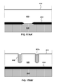
- FIG. 7 is a schematic diagram of a trench MOSFET device 700 according to aspects of the present disclosure. It should be noted that the device 700 may have a plurality of active device cells though only portions are shown in FIG. 7 .
- the trench MOSFET device 700 includes a lightly doped epitaxial layer of a first conductivity type 720 (e.g., N ⁇ ) formed on top of a heavily doped semiconductor substrate 710 of the same conductivity type (e.g., N+).
- a body region 730 of a second conductivity opposite to the substrate 710 and the epitaxial layer 720 (e.g., P type) is formed in portions of the lightly doped epitaxial layer 720 .
- a gate trench 740 filled with an electrically isolated gate electrodes 742 extends into the lightly doped epitaxial layer 720 .
- a heavily doped source region 750 of the same conductivity type as the substrate (e.g., N+) is formed proximate to the trenches within the body region 730 .
- the epitaxial layer 720 has an undulation 725 (or a recessed portion) along a channel width direction of the device 700 such that the epitaxial layer 720 has variations in depth along the channel width direction at the interface between the epitaxial layer 720 and the substrate 710 .
- the body region 730 has an undulation 735 along the channel width direction above the undulation 725 such that the body region 730 has variations in depth along the channel width direction at the interface between the body region 730 and the epitaxial layer 720 .
- the source region 750 has an undulation 755 along the channel width direction above the undulations 725 and 735 such that the source region 750 has variations in depth along the channel width direction at the interface between the source region 750 and the body region 730 .
- the undulations 725 , 735 and 755 each has a recessed bottom surface and tapered sides.
- the channel of the device 700 is “folded” as shown in FIG. 7 , and thus increasing channel width and reducing channel resistance.
- the channel resistance may be reduced 16.3% when the angle 790 of the tapered sides of the undulations 725 , 735 and 755 is at about 45 degree.
- the sharper the angle 790 the better the reduction improvement on channel resistance (R ch ).
- the tapered sides of the undulations 725 , 735 and 755 may be at an angle between about 25 degrees and about 90 degrees.
- FIGS. 8AA ′- 29 AA′ and FIGS. 8BB ′- 29 BB′ illustrate a process of fabricating a trench MOSFET in the A-A′ and B-B′ cross-sections in FIG. 7 respectively.
- the process uses a semiconductor substrate 810 of a first conductivity as a starting material.
- the substrate 810 can be a heavily doped N type (N+) silicon wafer.
- a thin epitaxial layer (EPI) 812 is then deposited on the N+ substrate 810 .
- the EPI 812 is a lightly-doped N-type layer of silicon.
- a buried layer mask 819 is applied on the EPI layer 812 , followed by an implant of a heavily-doped N type impurity (N+) to form a buried layer 814 .
- N+ heavily-doped N type impurity
- FIGS. 10AA ′ and 10 BB the impurity is then driven by, e.g., annealing. It is noted that the portion of the EPI 812 covered by the buried layer mask 819 is left exposed after the annealing process and removal of the buried layer mask 819 as shown in FIG. 10AA ′.
- a thick EPI layer 820 of the same conductivity type as the substrate 810 is provided over the substrate 810 as shown in FIGS. 11AA ′ and 11 BB′.
- the thick EPI layer 820 is a lightly doped N type layer.
- the thickness of the thick EPI layer 820 may be between about 1 ⁇ m and about 3 ⁇ m.
- the masking of the buried layer implant in the above step leads to a thicker and deeper region of the EPI layer 820 in the portion that is previously covered by the buried layer mask 819 , and thinner and shallower regions in the portions that are not covered by the buried layer mask 819 .
- the thicker and deeper region of the EPI layer 820 forms a first undulation.
- an insulating layer 822 is provided over the EPI layer 820 .
- the insulating layer 822 is an oxide layer.
- a photoresist (not shown) is then applied on the insulating layer 822 and patterned to define the gate trenches.
- the patterned photoresist includes openings at locations of the gate trenches.
- an etching process is performed to etch away portions of the insulating layer 822 that are exposed to an etchant through openings in the photoresist.
- the remaining portions of the insulating layer 822 act as a mask and corresponding portions of the underlying EPI layer 820 are etched down to form the gate trench 840 as shown in FIGS. 14AA ′ and 14 BB′. The remaining portions of the insulating layer 822 are then removed.
- a sacrificial oxide layer (not shown) may be grown and then removed to improve the silicon surface.
- An insulating layer (e.g., gate oxide) 824 is then formed over the EPI layer 820 and along the inner surface of the gate trenches 840 as shown in FIGS. 15AA ′ and 15 BB′.
- a conductive material 842 is deposited over the gate oxide layer 824 .
- the conductive material can be in-situ doped or undoped polysilicon.
- the conductive material 842 is then etched back forming the gate electrode 842 a as shown in FIGS. 17AA ′ and 17 BB′.
- An annealing process is then taken place in FIGS. 18AA ′ and 18 BB′.
- a thin layer of oxide 824 a is formed on top of the gate electrode 842 a by adding a little oxygen to the annealing recipe.
- a thin layer of a first insulating material 826 is deposited over the gate oxide layer 824 .
- the thickness of the thin layer of the first insulating material 826 lies in a range of 200 ⁇ to 500 ⁇ .
- a layer of a second insulating material 828 is deposited over the thin layer of the first insulating material 826 .
- the thickness of the layer of the second insulating material 828 is about 500 ⁇ to 1000 ⁇ .
- the thin layer 826 and the layer 828 are of two different insulating materials, each resistant to an etch process that etches the other.
- the thin layer of the first insulating material 826 is resistant to an etch process that etches the layer of the second insulating material 828 and vice versa.
- the thin layer of the first insulating material 826 may form an etch stop for subsequent etch on the layer of the second insulating material 828 .
- the thin layer 826 is a nitride layer
- the layer of a second insulating material 828 is an oxide layer.
- the insulating material 828 is treated such that the edges of the opening are sloped or tapered after etching.
- the surface can be doped or implanted to increase the etch rate to enhance undercutting for wet etching. If plasma etching is used, oxygen can be added during the etch to erode the photoresist to create the sloped edge.
- the slope of the opening can be tailored to the desired angle.
- a body mask 829 is applied for body implantation. It is noted that the body mask 829 has an opening shown in the A-A′ plane but not in the B-B′ plane.
- Dopants are implanted into the EPI layer 820 through the oxide layer 828 and the thin nitride layer 826 as shown in FIGS. 22AA ′- 22 BB′.
- the dopant ions are of the opposite conductivity type to the doping of the substrate 810 .
- the dopant ions can be Boron ions for an N-channel device.
- Phosphorous or Arsenic ions can be used for P-channel devices.
- the dopants can be implanted deeper into the EPI layer 820 under the opening to form the second undulation.
- the angle of the undulation follows the slope of the oxide opening. Heat is then applied to activate dopant atoms and drive dopant diffusion to form a body region 830 as shown in FIGS. 23AA ′ and 23 BB′.
- source implant and source diffusion take place.
- a source implant is carried out through the same opening as shown in FIGS. 24AA ′ and 24 BB′.
- the dopant ions are of the same conductivity type to the doping of the substrate 810 .
- Arsenic ions can be implanted for an N-channel device.
- Boron ion can be implanted for a P-channel device. Since the oxide layer 828 and the nitride layer 826 under the mask opening is not thick, the dopants can be implanted deeper in the body region 830 under the opening to form the third undulation.
- a dielectric layer 860 such as an oxide, can be deposited over the gate oxide layer 824 as shown in FIGS. 27AA ′- 27 BB′.
- the dielectric layer 860 is formed by a low temperature oxide followed by a layer of Borophosphorosilicate Glass (BPSG).
- BPSG Borophosphorosilicate Glass
- a contact photoresist 869 is then applied on the dielectric layer 860 with a pattern that has an opening at the locations of contact trenches.
- an etch process is performed to remove the uncovered portions of the dielectric layer 860 and form contact trenches 870 in the body region 830 .
- a barrier metal 872 is first lined with the inner surface of the contact trenches 870 .
- the barrier metal 872 may be Titanium (Ti) and Titanium Nitride (TiN).
- a conductive material such as Tungsten (W) may be blanket deposited in the contact trenches 870 followed by an etch back up to the surface of the dielectric layer 860 to form a conductive plug 874 .
- a metal layer 880 is deposited on the top as shown in FIGS. 29AA ′- 29 BB′.
- the metal layer 880 may be Aluminum (Al) or Aluminum Copper (AlCu).
Landscapes
- Engineering & Computer Science (AREA)
- Physics & Mathematics (AREA)
- Computer Hardware Design (AREA)
- Condensed Matter Physics & Semiconductors (AREA)
- General Physics & Mathematics (AREA)
- Microelectronics & Electronic Packaging (AREA)
- Power Engineering (AREA)
- Manufacturing & Machinery (AREA)
- High Energy & Nuclear Physics (AREA)
- Metal-Oxide And Bipolar Metal-Oxide Semiconductor Integrated Circuits (AREA)
- Geometry (AREA)
- Health & Medical Sciences (AREA)
- Toxicology (AREA)
- Insulated Gate Type Field-Effect Transistor (AREA)
- Electrodes Of Semiconductors (AREA)
Abstract
A trench MOSFET device includes a body, region and source region that undulate along a channel width direction of the MOSFET device such that the body region and source region have variations in depth along the channel width direction. The undulations increase a channel width of the MOSFET device.
Description
This disclosure relates to integrated circuits and more specifically to integrated circuit devices having field effect transistors (FETs).
Field Effect Transistors (FETs) are semiconductor transistor devices in which a voltage applied to an electrically insulated gate controls flow of current between source and drain. One example of a FET is a metal oxide semiconductor FET (MOSFET), in which a gate electrode is isolated from a semiconducting body region by an oxide insulator. When a voltage is applied to the gate, the resulting electric field generated penetrates through the oxide and creates an “inversion layer” or “channel” at the semiconductor-insulator interface. The inversion layer provides a channel through which current can pass. Varying the gate voltage modulates the conductivity of this layer and thereby controls the current flow between drain and source. MOSFETs may have different structures. In one example, MOSFETs may have a planar structure having gate, source and drain on the top of the device, with current flow taking place in a path parallel to the surface. In another example, MOSFETS may have a vertical structure in which a trench filled with doped polysilicon extends from the source to the drain with sidewalls and a floor that are each lined with a layer of thermally grown silicon dioxide. Such a trench MOSFET transistor allows less constricted current flow and, consequently, provides lower values of specific on-resistance.
FETs are useful in many power switching applications. In one particular configuration useful in a battery protection circuit module (PCM), two FETs are arranged in a back-to-back configuration with their drains connected together in a floating configuration. FIG. 1A schematically illustrates such a configuration. FIG. 1B shows use of such a device 100 in conjunction with a Battery Protection Circuit Module PCM 102, battery 104, and a load or charger 106. In this example, the gates of the charge and discharge FETs 120 and 130, respectively, are driven independently by a controller integrated circuit (IC) 110. This configuration allows for current control in both directions: charger to battery and battery to load. In normal charge and discharge operation both MOSFETs 120 and 130 are ON (i.e., conducting). During an overcharge or charge over-current condition of the battery 104, the controller IC 110 turns the charge FET 120 off and the discharge FET 130 on. During an over-discharge or discharge over-current condition, the controller IC 110 turns the charge FET 120 on and the discharge FET 130 off.
It is within this context that embodiments of the present invention arise.
Objects and advantages of aspects of the present disclosure will become apparent upon reading the following detailed description and upon reference to the accompanying drawings in which:
A cross-sectional view of the device 200 of FIG. 2A is shown in FIG. 2B . Each vertical MOSFET 220/230 includes a plurality of active device cells formed in a lightly-doped epitaxial layer 246 grown on a more heavily doped substrate 244. In this example, a heavily doped (e.g., N+) substrate 244 acts as a drain and the drains of the two MOSFETs 220 and 230 are electrically connected via back metal 242 formed on a backside of the substrate 244. Active devices are formed in a lesser doped epitaxial drift layer 246 of the same conductivity type (e.g., N-type) grown on the front side of the substrate 244. Body regions 250 of opposite conductivity to the substrate 244 and epitaxial region 246 (e.g., P-type) are formed in portions of the epitaxial layer 246. Trenches 252 are formed in the epitaxial layer 246 and then lined with an insulator 254 (e.g., an oxide). Electrically isolated gate electrodes 256, e.g., made of polycrystalline silicon (polysilicon, also known as poly) are disposed in the trenches 252. Heavily doped (e.g., N+) source regions 260 of the same conductivity type as the substrate 244 are formed proximate the trenches 252. External electrical contact to the source regions is made via a source metal layer 265 and vertical source contacts 267. The channel stops 280, 282 are formed using insulated electrodes similar to the gate electrodes that are shorted to the epitaxial drift region by source-type conductivity regions in the epitaxial region. The termination also includes guard rings 284, 286 formed by body-type conductivity regions.
A key characteristic of the device is the source-to-source resistance with both MOSFETs 220 and 230 turned on. It is desirable to make this resistance as small as possible. The total source-source resistance Rss is given by:
R ss=2R ch+2R drift +R backmetal+2R substrate,
where Rch is the resistance of the conductive channel through thesource 260 and body regions 250 when the gates are turned on, Rdrift is the resistance of the epitaxial layer 246, Rbackmetal is the resistance of the back metal 242, and Rsubstrate is the resistance of the substrate 244. Since the channel resistance (Rch) is one of the largest components of the total source-source resistance Rss, it is desirable to make the resistance of the conductive channel (Rch) as small as possible.
R ss=2R ch+2R drift +R backmetal+2R substrate,
where Rch is the resistance of the conductive channel through the
FinFET
Fin Field Effect Transistor (“FinFET”) is a type of non-planar transistors built on a silicon-on-insulator substrate. Hisamoto et al. in “A Folded-Channel MOSFET for Deep-Sub-Tenth Micron Era,”1032 IEDM (1998), introduces a FinFET structure which includes a vertical ultra-thin silicon fin, two gates self-aligned with the source and drain, a raised source and drain to reduce parasitic resistance, and a quasi-planar structure. FIG. 4 illustrates in perspective an improved FinFET transistor 400. The transistor 400 is constructed from a silicon body 402 that includes a drain region 404, a source region 406 and a fin-shaped channel region 408 connected between the drain region 404 and the source region 406. The drain 404, source 406 and the fin-channel regions 408 are covered by a dielectric layer 412. A gate structure 410 extends across and wrapped over the fin-shaped channel 408 such that the gate structure interface with three sides of the channel 408. The structure of the FinFET 400 provides improved electrical control over the channel conduction and it helps reduce leakage current levels and overcomes some other short-channel effects. In addition, it is noted that the channel width of a FinFET may be approximately double the height of the channel region fin by wrapping the gate over the channel 408. Since then, few methods have been proposed to increase the channel width of a planar MOSFET by folding the device such as the device 500 shown in FIG. 5 .
Folded Channel Trench MOSFET to Reduce Rss
To appreciate the advantages of a folded channel MOSFET in accordance with aspects of the present disclosure it is useful to understand a conventional trench MOSFET. FIG. 6 illustrates portions of a conventional trench MOSFET device 600. The trench MOSFET 600 includes a gate electrode 602, a body region 604 and a source region 606 provided over a substrate (not shown). It should be noted that although only one gate electrode 602 is shown in FIG. 6 , another gate electrode may be provided next to the side of the source region 606 a. The channel length (L) of the trench MOSFET 600 is between the bottom of the source region 606 and the bottom of the body region 604 (i.e., top of the substrate) and the channel width (W) is the third dimension of the cross-section as indicated. In order to improve total source-source resistance Rss by reducing channel resistance (Rch) of the trench MOSFET 600, it is desirable to reduce its channel length (L) or increase its channel width (W).
Aspects of the present disclosure achieve low channel resistance by “folding” the channel region of a trench MOSFET. FIG. 7 is a schematic diagram of a trench MOSFET device 700 according to aspects of the present disclosure. It should be noted that the device 700 may have a plurality of active device cells though only portions are shown in FIG. 7 . The trench MOSFET device 700 includes a lightly doped epitaxial layer of a first conductivity type 720 (e.g., N−) formed on top of a heavily doped semiconductor substrate 710 of the same conductivity type (e.g., N+). A body region 730 of a second conductivity opposite to the substrate 710 and the epitaxial layer 720 (e.g., P type) is formed in portions of the lightly doped epitaxial layer 720. A gate trench 740 filled with an electrically isolated gate electrodes 742 (e.g., polysilicon) extends into the lightly doped epitaxial layer 720. A heavily doped source region 750 of the same conductivity type as the substrate (e.g., N+) is formed proximate to the trenches within the body region 730.
As shown in FIG. 7 , the epitaxial layer 720 has an undulation 725 (or a recessed portion) along a channel width direction of the device 700 such that the epitaxial layer 720 has variations in depth along the channel width direction at the interface between the epitaxial layer 720 and the substrate 710. In addition, the body region 730 has an undulation 735 along the channel width direction above the undulation 725 such that the body region 730 has variations in depth along the channel width direction at the interface between the body region 730 and the epitaxial layer 720. The source region 750 has an undulation 755 along the channel width direction above the undulations 725 and 735 such that the source region 750 has variations in depth along the channel width direction at the interface between the source region 750 and the body region 730. As shown, the undulations 725, 735 and 755 each has a recessed bottom surface and tapered sides. With introduction of the undulations 725, 735 and 755, the channel of the device 700 is “folded” as shown in FIG. 7 , and thus increasing channel width and reducing channel resistance. In one example, the channel resistance may be reduced 16.3% when the angle 790 of the tapered sides of the undulations 725, 735 and 755 is at about 45 degree. It is noted that the sharper the angle 790, the better the reduction improvement on channel resistance (Rch). By way of example and not by way of limitation, the tapered sides of the undulations 725, 735 and 755 may be at an angle between about 25 degrees and about 90 degrees.
In FIGS. 12AA ′ and 12BB′, an insulating layer 822 is provided over the EPI layer 820. In some embodiment, the insulating layer 822 is an oxide layer. A photoresist (not shown) is then applied on the insulating layer 822 and patterned to define the gate trenches. The patterned photoresist includes openings at locations of the gate trenches. As shown in FIGS. 13AA ′ and 13BB′, an etching process is performed to etch away portions of the insulating layer 822 that are exposed to an etchant through openings in the photoresist. After the photoresist is removed, the remaining portions of the insulating layer 822 act as a mask and corresponding portions of the underlying EPI layer 820 are etched down to form the gate trench 840 as shown in FIGS. 14AA ′ and 14BB′. The remaining portions of the insulating layer 822 are then removed.
Next, a sacrificial oxide layer (not shown) may be grown and then removed to improve the silicon surface. An insulating layer (e.g., gate oxide) 824 is then formed over the EPI layer 820 and along the inner surface of the gate trenches 840 as shown in FIGS. 15AA ′ and 15BB′. In FIGS. 16AA ′ and 16BB′, a conductive material 842 is deposited over the gate oxide layer 824. In some embodiments, the conductive material can be in-situ doped or undoped polysilicon. The conductive material 842 is then etched back forming the gate electrode 842 a as shown in FIGS. 17AA ′ and 17BB′. An annealing process is then taken place in FIGS. 18AA ′ and 18BB′. As shown in FIG. 18BB ′, a thin layer of oxide 824 a is formed on top of the gate electrode 842 a by adding a little oxygen to the annealing recipe.
In FIGS. 19AA ′ and 19BB′, a thin layer of a first insulating material 826 is deposited over the gate oxide layer 824. In some embodiments, the thickness of the thin layer of the first insulating material 826 lies in a range of 200 Å to 500 Å. In FIGS. 20AA ′ and 20BB′, a layer of a second insulating material 828 is deposited over the thin layer of the first insulating material 826. In some embodiments, the thickness of the layer of the second insulating material 828 is about 500 Å to 1000 Å. The thin layer 826 and the layer 828 are of two different insulating materials, each resistant to an etch process that etches the other. That is, the thin layer of the first insulating material 826 is resistant to an etch process that etches the layer of the second insulating material 828 and vice versa. Thus, the thin layer of the first insulating material 826 may form an etch stop for subsequent etch on the layer of the second insulating material 828. In some embodiments, the thin layer 826 is a nitride layer, and the layer of a second insulating material 828 is an oxide layer. The insulating material 828 is treated such that the edges of the opening are sloped or tapered after etching. For example, the surface can be doped or implanted to increase the etch rate to enhance undercutting for wet etching. If plasma etching is used, oxygen can be added during the etch to erode the photoresist to create the sloped edge. Hence, the slope of the opening can be tailored to the desired angle.
Next, body implant and body diffusion take place. In FIGS. 21AA ′ and 21BB′, a body mask 829 is applied for body implantation. It is noted that the body mask 829 has an opening shown in the A-A′ plane but not in the B-B′ plane. Dopants are implanted into the EPI layer 820 through the oxide layer 828 and the thin nitride layer 826 as shown in FIGS. 22AA ′-22BB′. The dopant ions are of the opposite conductivity type to the doping of the substrate 810. In some embodiments, the dopant ions can be Boron ions for an N-channel device. In some embodiments, Phosphorous or Arsenic ions can be used for P-channel devices. Since the oxide layer 828 and the nitride layer 826 under the mask opening is not thick, the dopants can be implanted deeper into the EPI layer 820 under the opening to form the second undulation. The angle of the undulation follows the slope of the oxide opening. Heat is then applied to activate dopant atoms and drive dopant diffusion to form a body region 830 as shown in FIGS. 23AA ′ and 23BB′.
After forming the body region 830, source implant and source diffusion take place. First, a source implant is carried out through the same opening as shown in FIGS. 24AA ′ and 24BB′. The dopant ions are of the same conductivity type to the doping of the substrate 810. In some embodiments, Arsenic ions can be implanted for an N-channel device. Alternatively, Boron ion can be implanted for a P-channel device. Since the oxide layer 828 and the nitride layer 826 under the mask opening is not thick, the dopants can be implanted deeper in the body region 830 under the opening to form the third undulation. In FIGS. 25AA ′ and 25BB′, standard diffusion process is performed to form the source region 850 in the body region 830. Next, the oxide layer 828 and the nitride layer 826 are removed in FIGS. 26AA ′ and 26BB′ according to a standard process.
A dielectric layer 860, such as an oxide, can be deposited over the gate oxide layer 824 as shown in FIGS. 27AA ′-27BB′. In some embodiments, the dielectric layer 860 is formed by a low temperature oxide followed by a layer of Borophosphorosilicate Glass (BPSG).
A contact photoresist 869 is then applied on the dielectric layer 860 with a pattern that has an opening at the locations of contact trenches. In FIG. 28AA ′-28BB′, an etch process is performed to remove the uncovered portions of the dielectric layer 860 and form contact trenches 870 in the body region 830. In FIGS. 29AA ′-29BB′, a barrier metal 872 is first lined with the inner surface of the contact trenches 870. In some embodiments, the barrier metal 872 may be Titanium (Ti) and Titanium Nitride (TiN). A conductive material, such as Tungsten (W), may be blanket deposited in the contact trenches 870 followed by an etch back up to the surface of the dielectric layer 860 to form a conductive plug 874. Finally, a metal layer 880 is deposited on the top as shown in FIGS. 29AA ′-29BB′. In some embodiments, the metal layer 880 may be Aluminum (Al) or Aluminum Copper (AlCu).
While the above is a complete description of the preferred embodiments of the present invention, it is possible to use various alternatives, modifications, and equivalents. Therefore, the scope of the present invention should be determined not with reference to the above description but should, instead be determined with reference to the appended claims, along with their full scope of equivalents. Any feature, whether preferred or not, may be combined with any other feature, whether preferred or not. In the claims that follow, the indefinite article “A”, or “An” refers to a quantity of one or more of the item following the article, except where expressly stated otherwise. The appended claims are not to be interpreted as including means-plus-function limitations, unless such a limitation is explicitly recited in a given claim using the phrase “means for.” Any element in a claim that does not explicitly state “means for” performing a specified function, is not to be interpreted as a “means” or “step” clause as specified in 35 USC § 112, ¶6.
Claims (6)
1. A trench MOSFET device, comprising:
a lightly doped epitaxial layer of a first conductivity type provided on a heavily doped semiconductor substrate of the first conductivity type;
a gate trench filled with a conductive material extending into the lightly doped epitaxial layer;
a body region of a second conductivity type opposite to the first conductivity type provided in portions of the lightly doped epitaxial layer, wherein the body region have a first undulation along a channel width direction; and
a source region of the first conductivity type provided in top portions of the body region, wherein the source region have a second undulation along the channel width direction above the first undulation, wherein a channel width of the MOSFET device is increased with introduction of the first and second undulations wherein the lightly doped epitaxial layer has a third undulation along a channel width direction of the MOSFET device with a depth extending into the semiconductor substrate deeper than other portions of the lightly doped epitaxial layer.
2. The device of claim 1 , wherein the first conductivity type is an N type and the second conductivity type is a P type.
3. The device of claim 1 , wherein the lightly doped epitaxial layer, the body region and the source region have variations in depth along the channel width.
4. The device of claim 1 , wherein the first undulation has a depth extending into the lightly doped epitaxial layer deeper than other portions of the body region.
5. The device of claim 1 , wherein the second undulation has a depth extending into the body region deeper than other portions of the source region.
6. The device of claim 1 , wherein tapered sides of the first and second undulations are at an angle between about 25 degrees and about 90 degrees.
Priority Applications (3)
| Application Number | Priority Date | Filing Date | Title |
|---|---|---|---|
| US15/364,827 US10199492B2 (en) | 2016-11-30 | 2016-11-30 | Folded channel trench MOSFET |
| CN201711217259.1A CN108122988B (en) | 2016-11-30 | 2017-11-28 | Folded channel trench MOSFET |
| US16/264,540 US10553714B2 (en) | 2016-11-30 | 2019-01-31 | Method for fabricating a folded channel trench MOSFET |
Applications Claiming Priority (1)
| Application Number | Priority Date | Filing Date | Title |
|---|---|---|---|
| US15/364,827 US10199492B2 (en) | 2016-11-30 | 2016-11-30 | Folded channel trench MOSFET |
Related Child Applications (1)
| Application Number | Title | Priority Date | Filing Date |
|---|---|---|---|
| US16/264,540 Division US10553714B2 (en) | 2016-11-30 | 2019-01-31 | Method for fabricating a folded channel trench MOSFET |
Publications (2)
| Publication Number | Publication Date |
|---|---|
| US20180151720A1 US20180151720A1 (en) | 2018-05-31 |
| US10199492B2 true US10199492B2 (en) | 2019-02-05 |
Family
ID=62190508
Family Applications (2)
| Application Number | Title | Priority Date | Filing Date |
|---|---|---|---|
| US15/364,827 Active 2036-12-02 US10199492B2 (en) | 2016-11-30 | 2016-11-30 | Folded channel trench MOSFET |
| US16/264,540 Active US10553714B2 (en) | 2016-11-30 | 2019-01-31 | Method for fabricating a folded channel trench MOSFET |
Family Applications After (1)
| Application Number | Title | Priority Date | Filing Date |
|---|---|---|---|
| US16/264,540 Active US10553714B2 (en) | 2016-11-30 | 2019-01-31 | Method for fabricating a folded channel trench MOSFET |
Country Status (2)
| Country | Link |
|---|---|
| US (2) | US10199492B2 (en) |
| CN (1) | CN108122988B (en) |
Families Citing this family (1)
| Publication number | Priority date | Publication date | Assignee | Title |
|---|---|---|---|---|
| US10978559B1 (en) * | 2020-08-03 | 2021-04-13 | Texas Instruments Incorporated | MOS transistor with folded channel and folded drift region |
Citations (47)
| Publication number | Priority date | Publication date | Assignee | Title |
|---|---|---|---|---|
| JP2000323712A (en) * | 1999-04-30 | 2000-11-24 | Intersil Corp | Power MOS device having increased channel width and method of manufacturing the same |
| US6509233B2 (en) | 2000-10-13 | 2003-01-21 | Siliconix Incorporated | Method of making trench-gated MOSFET having cesium gate oxide layer |
| US6538300B1 (en) | 2000-09-14 | 2003-03-25 | Vishay Intertechnology, Inc. | Precision high-frequency capacitor formed on semiconductor substrate |
| US20040113201A1 (en) * | 2002-03-22 | 2004-06-17 | Siliconix Incorporated | Structures of and methods of fabricating trench-gated MIS devices |
| US20050280133A1 (en) | 2004-06-21 | 2005-12-22 | Alpha & Omega Semiconductor | Multiple device package |
| US20060289916A1 (en) * | 2004-10-07 | 2006-12-28 | Chanho Park | Power Trench MOSFETs Having SiGe/Si Channel Structure |
| US20080265241A1 (en) | 2007-04-26 | 2008-10-30 | Infineon Technologies Ag | Semiconductor device and a method for manufacturing a semiconductor device |
| US20090085103A1 (en) * | 2007-09-28 | 2009-04-02 | Infineon Technologies Austria Ag | Semiconductor device and method |
| US20090206924A1 (en) | 2008-02-14 | 2009-08-20 | Maxpower Semiconductor Inc. | Semiconductor Device Structures and Related Processes |
| TW200943449A (en) | 2008-04-10 | 2009-10-16 | Alpha & Omega Semiconductor Ltd | Structure for measuring body pinch resistance of high density trench MOSFET array |
| US7605425B2 (en) | 2005-02-11 | 2009-10-20 | Alpha & Omega Semiconductor Limited | Power MOS device |
| WO2010008617A1 (en) | 2008-07-15 | 2010-01-21 | Maxpower Semiconductor Inc. | Mosfet switch with embedded electrostatic charge |
| US20100078682A1 (en) * | 2008-09-29 | 2010-04-01 | Tat Ngai | Power mosfet having a strained channel in a semiconductor heterostructure on metal substrate |
| US20100321840A1 (en) * | 2009-06-17 | 2010-12-23 | Alpha & Omega Semiconductor, Inc. | Bottom source NMOS triggered zener clamp for configuring an ultra-low voltage transient voltage suppressor (TVS) |
| US20110049580A1 (en) | 2009-08-28 | 2011-03-03 | Sik Lui | Hybrid Packaged Gate Controlled Semiconductor Switching Device Using GaN MESFET |
| US20110180909A1 (en) | 2005-12-22 | 2011-07-28 | Fuji Electric Co., Ltd. | Semiconductor device |
| US8004063B2 (en) | 2000-09-14 | 2011-08-23 | Vishay Intertechnology, Inc. | Precision high-frequency capacitor formed on semiconductor substrate |
| US8357973B2 (en) | 2006-09-17 | 2013-01-22 | Alpha And Omega Semiconductor Incorporated | Inverted-trench grounded-source FET structure with trenched source body short electrode |
| US8394702B2 (en) | 2010-03-24 | 2013-03-12 | Alpha And Omega Semiconductor Incorporated | Method for making dual gate oxide trench MOSFET with channel stop using three or four masks process |
| US8431989B2 (en) | 2006-02-17 | 2013-04-30 | Alpha And Omega Semiconductor Incorporated | Shielded gate trench (SGT) MOSFET devices and manufacturing processes |
| US8431470B2 (en) | 2011-04-04 | 2013-04-30 | Alpha And Omega Semiconductor Incorporated | Approach to integrate Schottky in MOSFET |
| US20130105886A1 (en) | 2011-11-01 | 2013-05-02 | Alpha And Omega Semiconductor Incorporated | Two-dimensional shielded gate transistor device and method of manufacture |
| US8445370B2 (en) | 2006-09-30 | 2013-05-21 | Alpha And Omega Semiconductor Incorporated | Trench junction barrier controlled Schottky |
| US20130126966A1 (en) | 2010-03-24 | 2013-05-23 | Alpha And Omega Semiconductor Incorporated | Oxide terminated trench mosfet with three or four masks |
| US20130224919A1 (en) * | 2012-02-28 | 2013-08-29 | Yongping Ding | Method for making gate-oxide with step-graded thickness in trenched dmos device for reduced gate-to-drain capacitance |
| US8580667B2 (en) | 2010-12-14 | 2013-11-12 | Alpha And Omega Semiconductor Incorporated | Self aligned trench MOSFET with integrated diode |
| US8643135B2 (en) | 2011-05-31 | 2014-02-04 | Alpha And Omega Semiconductor Incorporated | Edge termination configurations for high voltage semiconductor power devices |
| US8669613B2 (en) | 2010-09-29 | 2014-03-11 | Alpha & Omega Semiconductor, Inc. | Semiconductor device die with integrated MOSFET and low forward voltage diode-connected enhancement mode JFET and method |
| US8753935B1 (en) | 2012-12-21 | 2014-06-17 | Alpha And Omega Semiconductor Incorporated | High frequency switching MOSFETs with low output capacitance using a depletable P-shield |
| US8829603B2 (en) | 2011-08-18 | 2014-09-09 | Alpha And Omega Semiconductor Incorporated | Shielded gate trench MOSFET package |
| US8896131B2 (en) | 2011-02-03 | 2014-11-25 | Alpha And Omega Semiconductor Incorporated | Cascode scheme for improved device switching behavior |
| US8901571B2 (en) * | 2009-03-25 | 2014-12-02 | Rohm Co., Ltd. | Semiconductor device |
| US8933506B2 (en) | 2011-01-31 | 2015-01-13 | Alpha And Omega Semiconductor Incorporated | Diode structures with controlled injection efficiency for fast switching |
| US8946942B2 (en) | 2008-03-03 | 2015-02-03 | Alpha And Omega Semiconductor Incorporated | Robust semiconductor power devices with design to protect transistor cells with slower switching speed |
| US8963233B2 (en) | 2005-05-09 | 2015-02-24 | Alpha And Omega Semiconductor Incorporated | Power MOSFET device structure for high frequency applications |
| US8963240B2 (en) | 2013-04-26 | 2015-02-24 | Alpha And Omega Semiconductor Incorporated | Shielded gate trench (SGT) mosfet devices and manufacturing processes |
| US20150060936A1 (en) | 2013-05-10 | 2015-03-05 | Yongping Ding | Process method and structure for high voltage mosfets |
| US20150084117A1 (en) * | 2009-06-17 | 2015-03-26 | Madhur Bobde | Bottom source nmos triggered zener clamp for configuring an ultra-low voltage transient voltage suppressor (tvs) |
| US9024378B2 (en) | 2013-02-09 | 2015-05-05 | Alpha And Omega Semiconductor Incorporated | Device structure and manufacturing method using HDP deposited source-body implant block |
| US9136380B2 (en) | 2012-12-21 | 2015-09-15 | Alpha And Omega Semiconductor Incorporated | Device structure and methods of making high density MOSFETs for load switch and DC-DC applications |
| US9171917B2 (en) | 2011-05-31 | 2015-10-27 | Alpha And Omega Semiconductor Incorporated | Edge termination configurations for high voltage semiconductor power devices |
| US20150311295A1 (en) | 2014-04-23 | 2015-10-29 | Alpha And Omega Semiconductor Incorporated | Split poly connection via through-poly-contact (tpc) in split-gate based power mosfets |
| US9190512B2 (en) | 2012-12-21 | 2015-11-17 | Alpha And Omega Semiconductor Incorporated | High density trench-based power MOSFETs with self-aligned active contacts and method for making such devices |
| US9230957B2 (en) | 2013-03-11 | 2016-01-05 | Alpha And Omega Semiconductor Incorporated | Integrated snubber in a single poly MOSFET |
| US9246347B2 (en) | 2010-09-29 | 2016-01-26 | Alpha And Omega Semiconductor Incorporated | Battery charging circuit with serial connection of MOSFET and an enhancement mode JFET configured as reverse blocking diode with low forward voltage drop |
| US9269805B2 (en) | 2013-11-14 | 2016-02-23 | Alpha And Omega Semiconductor Incorporated | Method to manufacture short channel trench MOSFET |
| US9484452B2 (en) | 2014-12-10 | 2016-11-01 | Alpha And Omega Semiconductor Incorporated | Integrating enhancement mode depleted accumulation/inversion channel devices with MOSFETs |
Family Cites Families (5)
| Publication number | Priority date | Publication date | Assignee | Title |
|---|---|---|---|---|
| JP2007042892A (en) * | 2005-08-03 | 2007-02-15 | Sharp Corp | Trench type MISFET |
| US20100200912A1 (en) * | 2009-02-11 | 2010-08-12 | Force Mos Technology Co. Ltd. | Mosfets with terrace irench gate and improved source-body contact |
| WO2013013698A1 (en) * | 2011-07-22 | 2013-01-31 | X-Fab Semiconductor Foundries Ag | A semiconductor device |
| US8669611B2 (en) * | 2012-07-11 | 2014-03-11 | Taiwan Semiconductor Manufacturing Company, Ltd. | Apparatus and method for power MOS transistor |
| US9293559B2 (en) * | 2013-07-31 | 2016-03-22 | Alpha And Omega Semiconductor Incorporated | Dual trench-gate IGBT structure |
-
2016
- 2016-11-30 US US15/364,827 patent/US10199492B2/en active Active
-
2017
- 2017-11-28 CN CN201711217259.1A patent/CN108122988B/en active Active
-
2019
- 2019-01-31 US US16/264,540 patent/US10553714B2/en active Active
Patent Citations (61)
| Publication number | Priority date | Publication date | Assignee | Title |
|---|---|---|---|---|
| JP2000323712A (en) * | 1999-04-30 | 2000-11-24 | Intersil Corp | Power MOS device having increased channel width and method of manufacturing the same |
| US6538300B1 (en) | 2000-09-14 | 2003-03-25 | Vishay Intertechnology, Inc. | Precision high-frequency capacitor formed on semiconductor substrate |
| US6621143B2 (en) | 2000-09-14 | 2003-09-16 | Vishay Intertechnology, Inc | Precision high-frequency capacitor on semiconductor substrate |
| US8004063B2 (en) | 2000-09-14 | 2011-08-23 | Vishay Intertechnology, Inc. | Precision high-frequency capacitor formed on semiconductor substrate |
| US9136060B2 (en) | 2000-09-14 | 2015-09-15 | Vishay-Siliconix | Precision high-frequency capacitor formed on semiconductor substrate |
| US6509233B2 (en) | 2000-10-13 | 2003-01-21 | Siliconix Incorporated | Method of making trench-gated MOSFET having cesium gate oxide layer |
| US20040113201A1 (en) * | 2002-03-22 | 2004-06-17 | Siliconix Incorporated | Structures of and methods of fabricating trench-gated MIS devices |
| US9324858B2 (en) | 2002-03-22 | 2016-04-26 | Vishay-Siliconix | Trench-gated MIS devices |
| US20050280133A1 (en) | 2004-06-21 | 2005-12-22 | Alpha & Omega Semiconductor | Multiple device package |
| US20060289916A1 (en) * | 2004-10-07 | 2006-12-28 | Chanho Park | Power Trench MOSFETs Having SiGe/Si Channel Structure |
| US7605425B2 (en) | 2005-02-11 | 2009-10-20 | Alpha & Omega Semiconductor Limited | Power MOS device |
| US7800169B2 (en) | 2005-02-11 | 2010-09-21 | Alpha And Omega Semiconductor Incorporated | Power MOS device |
| US8963233B2 (en) | 2005-05-09 | 2015-02-24 | Alpha And Omega Semiconductor Incorporated | Power MOSFET device structure for high frequency applications |
| US20110180909A1 (en) | 2005-12-22 | 2011-07-28 | Fuji Electric Co., Ltd. | Semiconductor device |
| US8431989B2 (en) | 2006-02-17 | 2013-04-30 | Alpha And Omega Semiconductor Incorporated | Shielded gate trench (SGT) MOSFET devices and manufacturing processes |
| US8357973B2 (en) | 2006-09-17 | 2013-01-22 | Alpha And Omega Semiconductor Incorporated | Inverted-trench grounded-source FET structure with trenched source body short electrode |
| US8445370B2 (en) | 2006-09-30 | 2013-05-21 | Alpha And Omega Semiconductor Incorporated | Trench junction barrier controlled Schottky |
| US20080265241A1 (en) | 2007-04-26 | 2008-10-30 | Infineon Technologies Ag | Semiconductor device and a method for manufacturing a semiconductor device |
| US20090085103A1 (en) * | 2007-09-28 | 2009-04-02 | Infineon Technologies Austria Ag | Semiconductor device and method |
| TW200945584A (en) | 2008-02-14 | 2009-11-01 | Maxpower Semiconductor Inc | Semiconductor device structures and related processes |
| US20090206924A1 (en) | 2008-02-14 | 2009-08-20 | Maxpower Semiconductor Inc. | Semiconductor Device Structures and Related Processes |
| US8946942B2 (en) | 2008-03-03 | 2015-02-03 | Alpha And Omega Semiconductor Incorporated | Robust semiconductor power devices with design to protect transistor cells with slower switching speed |
| US7683369B2 (en) | 2008-04-10 | 2010-03-23 | Alpha & Omega Semiconductor, Inc. | Structure for measuring body pinch resistance of high density trench MOSFET array |
| TW200943449A (en) | 2008-04-10 | 2009-10-16 | Alpha & Omega Semiconductor Ltd | Structure for measuring body pinch resistance of high density trench MOSFET array |
| WO2010008617A1 (en) | 2008-07-15 | 2010-01-21 | Maxpower Semiconductor Inc. | Mosfet switch with embedded electrostatic charge |
| US20100078682A1 (en) * | 2008-09-29 | 2010-04-01 | Tat Ngai | Power mosfet having a strained channel in a semiconductor heterostructure on metal substrate |
| US8901571B2 (en) * | 2009-03-25 | 2014-12-02 | Rohm Co., Ltd. | Semiconductor device |
| US20100321840A1 (en) * | 2009-06-17 | 2010-12-23 | Alpha & Omega Semiconductor, Inc. | Bottom source NMOS triggered zener clamp for configuring an ultra-low voltage transient voltage suppressor (TVS) |
| US20150084117A1 (en) * | 2009-06-17 | 2015-03-26 | Madhur Bobde | Bottom source nmos triggered zener clamp for configuring an ultra-low voltage transient voltage suppressor (tvs) |
| US20110049580A1 (en) | 2009-08-28 | 2011-03-03 | Sik Lui | Hybrid Packaged Gate Controlled Semiconductor Switching Device Using GaN MESFET |
| US9214545B2 (en) | 2010-03-24 | 2015-12-15 | Alpha And Omega Semiconductor Incorporated | Dual gate oxide trench MOSFET with channel stop trench |
| US20130126966A1 (en) | 2010-03-24 | 2013-05-23 | Alpha And Omega Semiconductor Incorporated | Oxide terminated trench mosfet with three or four masks |
| US8956940B2 (en) | 2010-03-24 | 2015-02-17 | Alpha And Omega Semiconductor Incorporated | Oxide terminated trench MOSFET with three or four masks |
| US8394702B2 (en) | 2010-03-24 | 2013-03-12 | Alpha And Omega Semiconductor Incorporated | Method for making dual gate oxide trench MOSFET with channel stop using three or four masks process |
| US8907416B2 (en) | 2010-03-24 | 2014-12-09 | Alpha And Omega Semiconductor Incorporated | Dual gate oxide trench MOSFET with channel stop trench |
| US8669613B2 (en) | 2010-09-29 | 2014-03-11 | Alpha & Omega Semiconductor, Inc. | Semiconductor device die with integrated MOSFET and low forward voltage diode-connected enhancement mode JFET and method |
| US9246347B2 (en) | 2010-09-29 | 2016-01-26 | Alpha And Omega Semiconductor Incorporated | Battery charging circuit with serial connection of MOSFET and an enhancement mode JFET configured as reverse blocking diode with low forward voltage drop |
| US8580667B2 (en) | 2010-12-14 | 2013-11-12 | Alpha And Omega Semiconductor Incorporated | Self aligned trench MOSFET with integrated diode |
| US8980716B2 (en) | 2010-12-14 | 2015-03-17 | Alpha And Omega Semiconductor Incorporated | Self aligned trench MOSFET with integrated diode |
| US8933506B2 (en) | 2011-01-31 | 2015-01-13 | Alpha And Omega Semiconductor Incorporated | Diode structures with controlled injection efficiency for fast switching |
| US8896131B2 (en) | 2011-02-03 | 2014-11-25 | Alpha And Omega Semiconductor Incorporated | Cascode scheme for improved device switching behavior |
| US8828857B2 (en) | 2011-04-04 | 2014-09-09 | Alpha And Omega Semiconductor Incorporated | Approach to integrate Schottky in MOSFET |
| US8431470B2 (en) | 2011-04-04 | 2013-04-30 | Alpha And Omega Semiconductor Incorporated | Approach to integrate Schottky in MOSFET |
| US8643135B2 (en) | 2011-05-31 | 2014-02-04 | Alpha And Omega Semiconductor Incorporated | Edge termination configurations for high voltage semiconductor power devices |
| US9171917B2 (en) | 2011-05-31 | 2015-10-27 | Alpha And Omega Semiconductor Incorporated | Edge termination configurations for high voltage semiconductor power devices |
| US8829603B2 (en) | 2011-08-18 | 2014-09-09 | Alpha And Omega Semiconductor Incorporated | Shielded gate trench MOSFET package |
| US8759908B2 (en) | 2011-11-01 | 2014-06-24 | Alpha And Omega Semiconductor Incorporated | Two-dimensional shielded gate transistor device and method of manufacture |
| US20130105886A1 (en) | 2011-11-01 | 2013-05-02 | Alpha And Omega Semiconductor Incorporated | Two-dimensional shielded gate transistor device and method of manufacture |
| US20130224919A1 (en) * | 2012-02-28 | 2013-08-29 | Yongping Ding | Method for making gate-oxide with step-graded thickness in trenched dmos device for reduced gate-to-drain capacitance |
| US9190512B2 (en) | 2012-12-21 | 2015-11-17 | Alpha And Omega Semiconductor Incorporated | High density trench-based power MOSFETs with self-aligned active contacts and method for making such devices |
| US9136380B2 (en) | 2012-12-21 | 2015-09-15 | Alpha And Omega Semiconductor Incorporated | Device structure and methods of making high density MOSFETs for load switch and DC-DC applications |
| US8753935B1 (en) | 2012-12-21 | 2014-06-17 | Alpha And Omega Semiconductor Incorporated | High frequency switching MOSFETs with low output capacitance using a depletable P-shield |
| US8946816B2 (en) | 2012-12-21 | 2015-02-03 | Alpha And Omega Semiconductor Incorporated | High frequency switching MOSFETs with low output capacitance using a depletable P-shield |
| US9024378B2 (en) | 2013-02-09 | 2015-05-05 | Alpha And Omega Semiconductor Incorporated | Device structure and manufacturing method using HDP deposited source-body implant block |
| US9230957B2 (en) | 2013-03-11 | 2016-01-05 | Alpha And Omega Semiconductor Incorporated | Integrated snubber in a single poly MOSFET |
| US8963240B2 (en) | 2013-04-26 | 2015-02-24 | Alpha And Omega Semiconductor Incorporated | Shielded gate trench (SGT) mosfet devices and manufacturing processes |
| US20150060936A1 (en) | 2013-05-10 | 2015-03-05 | Yongping Ding | Process method and structure for high voltage mosfets |
| US9269805B2 (en) | 2013-11-14 | 2016-02-23 | Alpha And Omega Semiconductor Incorporated | Method to manufacture short channel trench MOSFET |
| US20150311295A1 (en) | 2014-04-23 | 2015-10-29 | Alpha And Omega Semiconductor Incorporated | Split poly connection via through-poly-contact (tpc) in split-gate based power mosfets |
| US20160329426A1 (en) | 2014-04-23 | 2016-11-10 | Alpha And Omega Semiconductor Incorporated | Split poly connection via through-poly-contact (tpc) in split-gate based power mosfets |
| US9484452B2 (en) | 2014-12-10 | 2016-11-01 | Alpha And Omega Semiconductor Incorporated | Integrating enhancement mode depleted accumulation/inversion channel devices with MOSFETs |
Non-Patent Citations (2)
| Title |
|---|
| Hisamoto et al. in "A Folded-Channel MOSFET for Deep-Sub-Tenth Micron Era," 1032 IEDM (1998). |
| Office Action dated May 16, 2018 for Taiwanese patent application No. 10720440610. |
Also Published As
| Publication number | Publication date |
|---|---|
| US10553714B2 (en) | 2020-02-04 |
| CN108122988B (en) | 2021-06-22 |
| US20190172945A1 (en) | 2019-06-06 |
| US20180151720A1 (en) | 2018-05-31 |
| CN108122988A (en) | 2018-06-05 |
Similar Documents
| Publication | Publication Date | Title |
|---|---|---|
| TWI500114B (en) | Semiconductor component and manufacturing method | |
| US7833863B1 (en) | Method of manufacturing a closed cell trench MOSFET | |
| US9806175B2 (en) | Power MOSFET device structure for high frequency applications | |
| US8907394B2 (en) | Insulated gate semiconductor device having shield electrode structure | |
| TWI409950B (en) | Self-calibrating trench metal oxide semiconductor field effect transistor (MOSFET) and method of fabricating the same | |
| US8779510B2 (en) | Semiconductor power devices manufactured with self-aligned processes and more reliable electrical contacts | |
| US7344945B1 (en) | Method of manufacturing a drain side gate trench metal-oxide-semiconductor field effect transistor | |
| US7989293B2 (en) | Trench device structure and fabrication | |
| US20150349091A1 (en) | Semiconductor power devices manufactured with self-aligned processes and more reliable electrical contacts | |
| US20100264488A1 (en) | Low Qgd trench MOSFET integrated with schottky rectifier | |
| US7417298B2 (en) | High voltage insulated-gate transistor | |
| US20120261746A1 (en) | Double-Trench Vertical Devices and Methods with Self-Alignment Between Gate and Body Contact | |
| US8471331B2 (en) | Method of making an insulated gate semiconductor device with source-substrate connection and structure | |
| TWI629793B (en) | A source contact transistor cell semiconductor device having a trench, a semiconductor device manufacturing method, and an integrated circuit | |
| KR101332590B1 (en) | Power semiconductor device having improved performance and method | |
| US9449968B2 (en) | Method for manufacturing a semiconductor device and a semiconductor device | |
| US8575688B2 (en) | Trench device structure and fabrication | |
| US10553714B2 (en) | Method for fabricating a folded channel trench MOSFET | |
| JP6421337B2 (en) | Semiconductor device | |
| TWI650862B (en) | Folded channel trench mosfet | |
| JP2004063844A (en) | Semiconductor device and manufacturing method thereof | |
| CN106549056B (en) | Double-grid groove type power transistor and manufacturing method thereof |
Legal Events
| Date | Code | Title | Description |
|---|---|---|---|
| AS | Assignment |
Owner name: ALPHA AND OMEGA SEMICONDUCTOR INCORPORATED, CALIFO Free format text: ASSIGNMENT OF ASSIGNORS INTEREST;ASSIGNOR:LUI, SIK;REEL/FRAME:040809/0562 Effective date: 20161130 |
|
| STCF | Information on status: patent grant |
Free format text: PATENTED CASE |
|
| MAFP | Maintenance fee payment |
Free format text: PAYMENT OF MAINTENANCE FEE, 4TH YEAR, LARGE ENTITY (ORIGINAL EVENT CODE: M1551); ENTITY STATUS OF PATENT OWNER: LARGE ENTITY Year of fee payment: 4 |