US10197842B2 - Liquid crystal display device - Google Patents
Liquid crystal display device Download PDFInfo
- Publication number
- US10197842B2 US10197842B2 US15/483,513 US201715483513A US10197842B2 US 10197842 B2 US10197842 B2 US 10197842B2 US 201715483513 A US201715483513 A US 201715483513A US 10197842 B2 US10197842 B2 US 10197842B2
- Authority
- US
- United States
- Prior art keywords
- layer
- liquid crystal
- substrate
- display area
- display device
- Prior art date
- Legal status (The legal status is an assumption and is not a legal conclusion. Google has not performed a legal analysis and makes no representation as to the accuracy of the status listed.)
- Active
Links
Images


Classifications
-
- G—PHYSICS
- G02—OPTICS
- G02F—OPTICAL DEVICES OR ARRANGEMENTS FOR THE CONTROL OF LIGHT BY MODIFICATION OF THE OPTICAL PROPERTIES OF THE MEDIA OF THE ELEMENTS INVOLVED THEREIN; NON-LINEAR OPTICS; FREQUENCY-CHANGING OF LIGHT; OPTICAL LOGIC ELEMENTS; OPTICAL ANALOGUE/DIGITAL CONVERTERS
- G02F1/00—Devices or arrangements for the control of the intensity, colour, phase, polarisation or direction of light arriving from an independent light source, e.g. switching, gating or modulating; Non-linear optics
- G02F1/01—Devices or arrangements for the control of the intensity, colour, phase, polarisation or direction of light arriving from an independent light source, e.g. switching, gating or modulating; Non-linear optics for the control of the intensity, phase, polarisation or colour
- G02F1/13—Devices or arrangements for the control of the intensity, colour, phase, polarisation or direction of light arriving from an independent light source, e.g. switching, gating or modulating; Non-linear optics for the control of the intensity, phase, polarisation or colour based on liquid crystals, e.g. single liquid crystal display cells
- G02F1/133—Constructional arrangements; Operation of liquid crystal cells; Circuit arrangements
- G02F1/1333—Constructional arrangements; Manufacturing methods
- G02F1/1335—Structural association of cells with optical devices, e.g. polarisers or reflectors
- G02F1/133509—Filters, e.g. light shielding masks
- G02F1/133512—Light shielding layers, e.g. black matrix
-
- G—PHYSICS
- G02—OPTICS
- G02F—OPTICAL DEVICES OR ARRANGEMENTS FOR THE CONTROL OF LIGHT BY MODIFICATION OF THE OPTICAL PROPERTIES OF THE MEDIA OF THE ELEMENTS INVOLVED THEREIN; NON-LINEAR OPTICS; FREQUENCY-CHANGING OF LIGHT; OPTICAL LOGIC ELEMENTS; OPTICAL ANALOGUE/DIGITAL CONVERTERS
- G02F1/00—Devices or arrangements for the control of the intensity, colour, phase, polarisation or direction of light arriving from an independent light source, e.g. switching, gating or modulating; Non-linear optics
- G02F1/01—Devices or arrangements for the control of the intensity, colour, phase, polarisation or direction of light arriving from an independent light source, e.g. switching, gating or modulating; Non-linear optics for the control of the intensity, phase, polarisation or colour
- G02F1/13—Devices or arrangements for the control of the intensity, colour, phase, polarisation or direction of light arriving from an independent light source, e.g. switching, gating or modulating; Non-linear optics for the control of the intensity, phase, polarisation or colour based on liquid crystals, e.g. single liquid crystal display cells
- G02F1/133—Constructional arrangements; Operation of liquid crystal cells; Circuit arrangements
- G02F1/1333—Constructional arrangements; Manufacturing methods
- G02F1/133345—Insulating layers
-
- G—PHYSICS
- G02—OPTICS
- G02F—OPTICAL DEVICES OR ARRANGEMENTS FOR THE CONTROL OF LIGHT BY MODIFICATION OF THE OPTICAL PROPERTIES OF THE MEDIA OF THE ELEMENTS INVOLVED THEREIN; NON-LINEAR OPTICS; FREQUENCY-CHANGING OF LIGHT; OPTICAL LOGIC ELEMENTS; OPTICAL ANALOGUE/DIGITAL CONVERTERS
- G02F1/00—Devices or arrangements for the control of the intensity, colour, phase, polarisation or direction of light arriving from an independent light source, e.g. switching, gating or modulating; Non-linear optics
- G02F1/01—Devices or arrangements for the control of the intensity, colour, phase, polarisation or direction of light arriving from an independent light source, e.g. switching, gating or modulating; Non-linear optics for the control of the intensity, phase, polarisation or colour
- G02F1/13—Devices or arrangements for the control of the intensity, colour, phase, polarisation or direction of light arriving from an independent light source, e.g. switching, gating or modulating; Non-linear optics for the control of the intensity, phase, polarisation or colour based on liquid crystals, e.g. single liquid crystal display cells
- G02F1/133—Constructional arrangements; Operation of liquid crystal cells; Circuit arrangements
- G02F1/1333—Constructional arrangements; Manufacturing methods
- G02F1/1337—Surface-induced orientation of the liquid crystal molecules, e.g. by alignment layers
-
- G—PHYSICS
- G02—OPTICS
- G02F—OPTICAL DEVICES OR ARRANGEMENTS FOR THE CONTROL OF LIGHT BY MODIFICATION OF THE OPTICAL PROPERTIES OF THE MEDIA OF THE ELEMENTS INVOLVED THEREIN; NON-LINEAR OPTICS; FREQUENCY-CHANGING OF LIGHT; OPTICAL LOGIC ELEMENTS; OPTICAL ANALOGUE/DIGITAL CONVERTERS
- G02F1/00—Devices or arrangements for the control of the intensity, colour, phase, polarisation or direction of light arriving from an independent light source, e.g. switching, gating or modulating; Non-linear optics
- G02F1/01—Devices or arrangements for the control of the intensity, colour, phase, polarisation or direction of light arriving from an independent light source, e.g. switching, gating or modulating; Non-linear optics for the control of the intensity, phase, polarisation or colour
- G02F1/13—Devices or arrangements for the control of the intensity, colour, phase, polarisation or direction of light arriving from an independent light source, e.g. switching, gating or modulating; Non-linear optics for the control of the intensity, phase, polarisation or colour based on liquid crystals, e.g. single liquid crystal display cells
- G02F1/133—Constructional arrangements; Operation of liquid crystal cells; Circuit arrangements
- G02F1/1333—Constructional arrangements; Manufacturing methods
- G02F1/1339—Gaskets; Spacers; Sealing of cells
- G02F1/13394—Gaskets; Spacers; Sealing of cells spacers regularly patterned on the cell subtrate, e.g. walls, pillars
-
- G—PHYSICS
- G02—OPTICS
- G02F—OPTICAL DEVICES OR ARRANGEMENTS FOR THE CONTROL OF LIGHT BY MODIFICATION OF THE OPTICAL PROPERTIES OF THE MEDIA OF THE ELEMENTS INVOLVED THEREIN; NON-LINEAR OPTICS; FREQUENCY-CHANGING OF LIGHT; OPTICAL LOGIC ELEMENTS; OPTICAL ANALOGUE/DIGITAL CONVERTERS
- G02F1/00—Devices or arrangements for the control of the intensity, colour, phase, polarisation or direction of light arriving from an independent light source, e.g. switching, gating or modulating; Non-linear optics
- G02F1/01—Devices or arrangements for the control of the intensity, colour, phase, polarisation or direction of light arriving from an independent light source, e.g. switching, gating or modulating; Non-linear optics for the control of the intensity, phase, polarisation or colour
- G02F1/13—Devices or arrangements for the control of the intensity, colour, phase, polarisation or direction of light arriving from an independent light source, e.g. switching, gating or modulating; Non-linear optics for the control of the intensity, phase, polarisation or colour based on liquid crystals, e.g. single liquid crystal display cells
- G02F1/133—Constructional arrangements; Operation of liquid crystal cells; Circuit arrangements
- G02F1/1333—Constructional arrangements; Manufacturing methods
- G02F1/1343—Electrodes
- G02F1/13439—Electrodes characterised by their electrical, optical, physical properties; materials therefor; method of making
-
- G—PHYSICS
- G02—OPTICS
- G02F—OPTICAL DEVICES OR ARRANGEMENTS FOR THE CONTROL OF LIGHT BY MODIFICATION OF THE OPTICAL PROPERTIES OF THE MEDIA OF THE ELEMENTS INVOLVED THEREIN; NON-LINEAR OPTICS; FREQUENCY-CHANGING OF LIGHT; OPTICAL LOGIC ELEMENTS; OPTICAL ANALOGUE/DIGITAL CONVERTERS
- G02F1/00—Devices or arrangements for the control of the intensity, colour, phase, polarisation or direction of light arriving from an independent light source, e.g. switching, gating or modulating; Non-linear optics
- G02F1/01—Devices or arrangements for the control of the intensity, colour, phase, polarisation or direction of light arriving from an independent light source, e.g. switching, gating or modulating; Non-linear optics for the control of the intensity, phase, polarisation or colour
- G02F1/13—Devices or arrangements for the control of the intensity, colour, phase, polarisation or direction of light arriving from an independent light source, e.g. switching, gating or modulating; Non-linear optics for the control of the intensity, phase, polarisation or colour based on liquid crystals, e.g. single liquid crystal display cells
- G02F1/133—Constructional arrangements; Operation of liquid crystal cells; Circuit arrangements
- G02F1/136—Liquid crystal cells structurally associated with a semi-conducting layer or substrate, e.g. cells forming part of an integrated circuit
- G02F1/1362—Active matrix addressed cells
- G02F1/136286—Wiring, e.g. gate line, drain line
-
- G—PHYSICS
- G02—OPTICS
- G02F—OPTICAL DEVICES OR ARRANGEMENTS FOR THE CONTROL OF LIGHT BY MODIFICATION OF THE OPTICAL PROPERTIES OF THE MEDIA OF THE ELEMENTS INVOLVED THEREIN; NON-LINEAR OPTICS; FREQUENCY-CHANGING OF LIGHT; OPTICAL LOGIC ELEMENTS; OPTICAL ANALOGUE/DIGITAL CONVERTERS
- G02F1/00—Devices or arrangements for the control of the intensity, colour, phase, polarisation or direction of light arriving from an independent light source, e.g. switching, gating or modulating; Non-linear optics
- G02F1/01—Devices or arrangements for the control of the intensity, colour, phase, polarisation or direction of light arriving from an independent light source, e.g. switching, gating or modulating; Non-linear optics for the control of the intensity, phase, polarisation or colour
- G02F1/13—Devices or arrangements for the control of the intensity, colour, phase, polarisation or direction of light arriving from an independent light source, e.g. switching, gating or modulating; Non-linear optics for the control of the intensity, phase, polarisation or colour based on liquid crystals, e.g. single liquid crystal display cells
- G02F1/133—Constructional arrangements; Operation of liquid crystal cells; Circuit arrangements
- G02F1/136—Liquid crystal cells structurally associated with a semi-conducting layer or substrate, e.g. cells forming part of an integrated circuit
- G02F1/1362—Active matrix addressed cells
- G02F1/1368—Active matrix addressed cells in which the switching element is a three-electrode device
-
- G—PHYSICS
- G02—OPTICS
- G02F—OPTICAL DEVICES OR ARRANGEMENTS FOR THE CONTROL OF LIGHT BY MODIFICATION OF THE OPTICAL PROPERTIES OF THE MEDIA OF THE ELEMENTS INVOLVED THEREIN; NON-LINEAR OPTICS; FREQUENCY-CHANGING OF LIGHT; OPTICAL LOGIC ELEMENTS; OPTICAL ANALOGUE/DIGITAL CONVERTERS
- G02F1/00—Devices or arrangements for the control of the intensity, colour, phase, polarisation or direction of light arriving from an independent light source, e.g. switching, gating or modulating; Non-linear optics
- G02F1/01—Devices or arrangements for the control of the intensity, colour, phase, polarisation or direction of light arriving from an independent light source, e.g. switching, gating or modulating; Non-linear optics for the control of the intensity, phase, polarisation or colour
- G02F1/13—Devices or arrangements for the control of the intensity, colour, phase, polarisation or direction of light arriving from an independent light source, e.g. switching, gating or modulating; Non-linear optics for the control of the intensity, phase, polarisation or colour based on liquid crystals, e.g. single liquid crystal display cells
- G02F1/133—Constructional arrangements; Operation of liquid crystal cells; Circuit arrangements
- G02F1/1333—Constructional arrangements; Manufacturing methods
- G02F1/133388—Constructional arrangements; Manufacturing methods with constructional differences between the display region and the peripheral region
-
- G—PHYSICS
- G02—OPTICS
- G02F—OPTICAL DEVICES OR ARRANGEMENTS FOR THE CONTROL OF LIGHT BY MODIFICATION OF THE OPTICAL PROPERTIES OF THE MEDIA OF THE ELEMENTS INVOLVED THEREIN; NON-LINEAR OPTICS; FREQUENCY-CHANGING OF LIGHT; OPTICAL LOGIC ELEMENTS; OPTICAL ANALOGUE/DIGITAL CONVERTERS
- G02F1/00—Devices or arrangements for the control of the intensity, colour, phase, polarisation or direction of light arriving from an independent light source, e.g. switching, gating or modulating; Non-linear optics
- G02F1/01—Devices or arrangements for the control of the intensity, colour, phase, polarisation or direction of light arriving from an independent light source, e.g. switching, gating or modulating; Non-linear optics for the control of the intensity, phase, polarisation or colour
- G02F1/13—Devices or arrangements for the control of the intensity, colour, phase, polarisation or direction of light arriving from an independent light source, e.g. switching, gating or modulating; Non-linear optics for the control of the intensity, phase, polarisation or colour based on liquid crystals, e.g. single liquid crystal display cells
- G02F1/133—Constructional arrangements; Operation of liquid crystal cells; Circuit arrangements
- G02F1/1333—Constructional arrangements; Manufacturing methods
- G02F1/1335—Structural association of cells with optical devices, e.g. polarisers or reflectors
- G02F1/133509—Filters, e.g. light shielding masks
- G02F1/133514—Colour filters
- G02F1/133519—Overcoatings
-
- G—PHYSICS
- G02—OPTICS
- G02F—OPTICAL DEVICES OR ARRANGEMENTS FOR THE CONTROL OF LIGHT BY MODIFICATION OF THE OPTICAL PROPERTIES OF THE MEDIA OF THE ELEMENTS INVOLVED THEREIN; NON-LINEAR OPTICS; FREQUENCY-CHANGING OF LIGHT; OPTICAL LOGIC ELEMENTS; OPTICAL ANALOGUE/DIGITAL CONVERTERS
- G02F1/00—Devices or arrangements for the control of the intensity, colour, phase, polarisation or direction of light arriving from an independent light source, e.g. switching, gating or modulating; Non-linear optics
- G02F1/01—Devices or arrangements for the control of the intensity, colour, phase, polarisation or direction of light arriving from an independent light source, e.g. switching, gating or modulating; Non-linear optics for the control of the intensity, phase, polarisation or colour
- G02F1/13—Devices or arrangements for the control of the intensity, colour, phase, polarisation or direction of light arriving from an independent light source, e.g. switching, gating or modulating; Non-linear optics for the control of the intensity, phase, polarisation or colour based on liquid crystals, e.g. single liquid crystal display cells
- G02F1/133—Constructional arrangements; Operation of liquid crystal cells; Circuit arrangements
- G02F1/1333—Constructional arrangements; Manufacturing methods
- G02F1/1337—Surface-induced orientation of the liquid crystal molecules, e.g. by alignment layers
- G02F1/133738—Surface-induced orientation of the liquid crystal molecules, e.g. by alignment layers for homogeneous alignment
-
- G02F2001/133388—
-
- G02F2001/133519—
-
- G02F2001/133738—
-
- G—PHYSICS
- G02—OPTICS
- G02F—OPTICAL DEVICES OR ARRANGEMENTS FOR THE CONTROL OF LIGHT BY MODIFICATION OF THE OPTICAL PROPERTIES OF THE MEDIA OF THE ELEMENTS INVOLVED THEREIN; NON-LINEAR OPTICS; FREQUENCY-CHANGING OF LIGHT; OPTICAL LOGIC ELEMENTS; OPTICAL ANALOGUE/DIGITAL CONVERTERS
- G02F2201/00—Constructional arrangements not provided for in groups G02F1/00 - G02F7/00
- G02F2201/12—Constructional arrangements not provided for in groups G02F1/00 - G02F7/00 electrode
- G02F2201/123—Constructional arrangements not provided for in groups G02F1/00 - G02F7/00 electrode pixel
-
- G—PHYSICS
- G02—OPTICS
- G02F—OPTICAL DEVICES OR ARRANGEMENTS FOR THE CONTROL OF LIGHT BY MODIFICATION OF THE OPTICAL PROPERTIES OF THE MEDIA OF THE ELEMENTS INVOLVED THEREIN; NON-LINEAR OPTICS; FREQUENCY-CHANGING OF LIGHT; OPTICAL LOGIC ELEMENTS; OPTICAL ANALOGUE/DIGITAL CONVERTERS
- G02F2202/00—Materials and properties
- G02F2202/02—Materials and properties organic material
Definitions
- Embodiments described herein relate generally to a liquid crystal display.
- Liquid crystal displays are used in various fields as display devices.
- Color liquid crystal displays comprise color filters.
- Light shielding layers are disposed between color filters of different colors to function of prevention color mixture in an oblique visual field.
- a liquid crystal display comprises an overcoat layer to cover a color filter, and a light-shielding layer disposed on a surface of the overcoat layer, which is on the liquid crystal layer.
- display devices each include a display area which displays images and a non-display area which surrounds the display area.
- the non-display area may look brighter than the display area when the display is turned OFF, it is known that different coloring layers and light-shielding coloring layers are stacked on the non-display area.
- FIG. 1 is a diagram showing a structure of a display panel of a display device and an equivalent circuit thereof according to an embodiment.
- FIG. 2 is a cross section showing a pixel of a display area of the display device and a layer structure thereof, shown in FIG. 1 .
- FIG. 3 is an enlarged view of an area A of the display panel shown in FIG. 1 .
- FIG. 4 is a cross section of the display panel taken along line B-C in FIG. 3 .
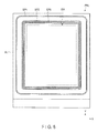
- FIG. 5 is a plan view showing the display panel shown in FIG. 1 , indicating the positions of spacers.
- FIG. 6 is a plan view showing the display panel shown in FIG. 1 , indicating the positions of slits formed in the light-shielding layer.
- FIG. 7 is a cross section showing a modification of the display device of the embodiment.
- FIG. 8 is a plan view showing the display panel shown in FIG. 1 , indicating the positions of recess portions.
- FIG. 9 is a cross section showing the first modification of the recess portions of the embodiment.
- FIG. 10 is a cross section showing the second modification of the recess portions of the embodiment.
- FIG. 11 is a cross section showing the third modification of the recess portions of the embodiment.
- a liquid crystal display device comprises a first substrate including a switching element and a pixel electrode; a second substrate including an insulating substrate, an organic layer which covers the insulating substrate in a non-display area in a shape of a frame surrounding a display area and comprises a first recess portion formed therein, and a light-shielding layer which covers the first recess portion; a sealing member which attaches the first substrate and the second substrate in the non-display area; and a liquid crystal layer disposed in a space surrounded by the first substrate, the second substrate and the sealing member.
- FIG. 1 is a diagram showing a structure of a display panel PNL of a display device DSP and an equivalent circuit thereof, according to this embodiment. The embodiment will be described on an assumption case where the display device DSP is a liquid crystal display.
- FIG. 1 is a plan view of the display panel PNL in an X-Y plane defined along a first direction X and a second direction Y, which cross each other.
- first direction X and the second direction Y cross each other orthogonally, but they may cross at an angle other than 90 degree.
- the display panel PNL comprises a first substrate SUB 1 , a second substrate SUB 2 disposed to oppose the first substrate SUB 1 and a liquid crystal layer LQ held between the first substrate SUB 1 and the second substrate SUB 2 .
- the first substrate SUB 1 and the second substrate SUB 2 are attached together with a sealing member SL while keeping a predetermined cell gap therebetween.
- the liquid crystal layer LQ is held in an inner portion surrounded by the sealing member SL in the cell gap between the first substrate SUB 1 and the second substrate SUB 2 .
- the display panel PNL comprises a display area DA which displays images to the inner portion surrounded by the sealing member SL.
- the display area DA has approximately a rectangular shape, for example, and a plurality of pixels PX arranged in a matrix are disposed in the display area DA.
- the display area DA may have some other polygonal shape, and further, edges thereof may be curved.
- the first substrate SUB 1 comprises, in the display area DA, gate lines G extending along the first direction X, source lines S extending along the second direction Y, switching elements SW each electrically connected to a respective gate line G and a respective source line S in a respective pixel PX, pixel electrodes PE each electrically connected to a switching element SW in a respective pixel PX, etc.
- a common electrode CE is included in the first substrate SUB 1 .
- the display panel PNL may be configured as a transmissive type which displays images by selectively transmitting light from a backlight unit placed on its, rear surface side, or a reflective type which displays images by selectively reflecting external light entering the display panel PNL, or a trans-reflective type which is a combination of the transmission type and reflection type.
- Signal supply sources necessary to drive the display panels PNL such as a drive IC chip 2 and a flexible printed circuit (FPC) substrate 3 are located in the non-display area NDA surrounding the display area DA as a frame.
- the drive IC chip 2 and the FPC substrate 3 are mounted in a mounting portion MT of the first substrate SUB 1 , which extends out from one substrate side edge SUB 2 e of the second substrate SUB 2 .
- the mounting portion MT is formed along with one substrate side edge SUB 1 e of the first substrate SUB 1 .
- the first substrate SUB 1 comprises, in the mounting portion MT, a pad to connect it to the signal supply sources.
- the pad includes the gate lines G, source lines S, etc. described above, which are electrically connected.
- the other three substrate-side edges of the second substrate SUB 2 oppose the other three substrate-side edges of the first substrate SUB 1 .
- the sealing member SL is formed on the non-display area NDA to have a frame shape which encloses the display area DA.
- the sealing member SL is formed into a rectangular shape in the example illustrated.
- the sealing member SL includes a first seal portion SL 1 , a second seal portion SL 2 , a third seal portion SL 3 and a fourth seal portion SL 4 .
- the seal portion SL 1 and the fourth seal portion SL 4 each extend along the first direction X and they oppose each other while interposing the display area DA therebetween.
- the second seal portion SL 2 and the third seal portion SL 3 each extend along the second direction Y and they oppose each other while interposing the display area DA therebetween.
- the first seal portion SL 1 is arranged along with the mounting portion MT.
- a width W 10 of the first seal portion SL 1 along the second direction Y is larger than a width W 20 of the fourth seal portion SL 4 along the second direction Y.
- a width of the second seal portion SL 2 along the first direction X and a width of the third seal portion SL 3 along the first direction X are equivalent in dimension to the width W 20 of the fourth seal portion SL 4 . That is, the first seal portion SL 1 is arranged on a mounting portion MT side, and therefore is formed to be wider than the second seal portion SL 2 , the third seal portion SL 3 and the fourth seal portion SL 4 .
- FIG. 2 is a cross section showing a pixel PX of the display area DA of the display device DSP shown in FIG. 1 and the layer structure thereof.
- both of pixel electrode PE and common electrode CE are provided on the first substrate SUB 1 , and they are applied to modes which use a lateral electric field along the main plane of the substrate, such as In-Plane Switching (IPS) mode and Fringe Field Switching (FFS) mode, which is one type of the IPS mode.
- IPS In-Plane Switching
- FFS Fringe Field Switching
- the positive direction of the third direction Z or the direction from the first substrate SUB 1 to the second substrate SUB 2 is defined as upward or above
- the negative direction of the third direction Z or the direction from the second substrate SUB 2 to the first substrate SUB 1 is defined as downward or below.
- the second member above the first member and “the second member below the first member” the second member may be in contact with the first member or may be separated from the first member.
- the third member may be interposed between the first member and the second member.
- the second member on the first member” and “the second member under the first member the second member is in contact with the first member.
- the first substrate SUB 1 comprises a first insulating substrate 10 , a switching element SW, a common electrode CE, a pixel electrode PE, a first insulating film 11 , a second insulating film 12 , a third insulating film 13 , a fourth insulating film 14 , a fifth insulating film 15 , a first alignment film AL 1 and the like.
- the first insulating substrate 10 is a light-transmissive substrate such as a glass or resin substrate.
- the first insulating film 11 covers the first insulating substrate 10 .
- a semiconductor layer SC of the switching element SW is located on the first insulating film 11 and is covered by the second insulating film 12 .
- the second insulating film 12 is located also on the first insulating film 11 .
- a gate electrode WG of the switching element SW is formed to be integrated with the gate line G on the second insulating film 12 , and is located above the semiconductor layer SC.
- the gate electrode WG is covered by the third insulating film 13 with the gate line G.
- the third insulating film 13 is located also on the second insulating film 12 .
- a source electrode WS and a drain electrode WD of the switching element SW are formed on the third insulating film 13 . Further, a source line S is similarly formed on the third insulating film 13 .
- the source electrode WS is formed to be integrated with the source line S.
- the source electrode WS is in contact with the semiconductor layer SC through a contact hole CH 1 which penetrates the second insulating film 12 and the third insulating film 13 .
- the drain electrode WD is in contact with the semiconductor layer SC through a contact hole CH 2 which penetrates the second insulating film 12 and the third insulating film 13 .
- the fourth insulating film 14 covers the switching element SW and the source line S.
- the fourth insulating film 14 is located also on the third insulating film 13 .
- the common electrode CE is formed on the fourth insulating film 14 .
- the common electrode CE is a transparent electrode formed from a transparent conductive material such as indium-tin-oxide (ITO) or indium zinc oxide (IZO).
- the fifth insulating film 15 covers the common electrode CE.
- the fifth insulating film 15 is located also on the fourth insulating film 14 .
- the pixel electrode PE is formed on the fifth insulating film 15 in a position to oppose the common electrode CE.
- the pixel electrode PE comprises slits 100 .
- the slits 100 are each formed above the common electrode CE.
- the pixel electrode PE is a transparent electrode formed from a transparent conductive material, for example, ITO or IZO.
- the pixel electrode PE is in contact with the drain electrode WD of the switching element SW through a contact hole CH 3 .
- the contact hole CH 3 comprises a contact hole CH 31 penetrating the fourth insulating film 14 to the drain electrode WD and a contact hole CH 32 penetrating the fifth insulating film 15 to the drain electrode WD.
- the first alignment film AL 1 covers the pixel electrode PE.
- the first alignment film AL 1 also covers the fifth insulating film 15 .
- the first alignment film AL 1 is formed from a material which exhibits horizontal alignment property and disposed on a surface of the first substrate SUB 1 , which is in contact with the liquid crystal layer LQ.
- the first insulating films 11 , the second insulating film 12 , the third insulating film 13 , and the fifth insulating film 15 described above are each formed from, for example, an inorganic material such as silicon oxide and silicon nitride.
- the fourth insulating film 14 is formed from, for example, an organic material such as a transparent resin.
- the second substrate SUB 2 comprises a second insulating substrate 20 , color filters CF, an overcoat layer OC, a light-shielding layer BM, a second alignment film AL 2 and the like.
- the second insulating substrate 20 is a light-transmissive substrate such as a glass or resin substrate.
- the color filters CF are disposed on an inner surface 20 A of the second insulating substrate 20 .
- the color filters CF are formed from resin materials colored in a plurality of colors different from each other, for example, red, blue and green.
- a red color filter CFR is disposed to correspond to a red pixel
- a green color filter CFG is disposed to correspond to a green pixel
- a blue color filter CFB is disposed to correspond to a blue pixel.
- the overcoat layer OC covers the color filters CF.
- the overcoat layer OC flattens unevenness on the surfaces of the color filters CF.
- the overcoat layer OC is formed from a transparent resin material.
- the light-shielding layer BM is disposed on a surface of the overcoat layer OC, which is on a side opposing the first substrate SUB 1 .
- the light-shielding layer BM is located to partition into pixels PX and oppose the wiring lines of the first substrate SUB 1 such as the gate line G, source line S and switching element SW and the contact hole CH 3 .
- the light-shielding layer BM formed to oppose each of the gate line G and source line S has a shape of lattice.
- the boundaries between adjacent color filters CF of different colors are located to overlay on the light-shielding layer BM.
- the second alignment film AL 2 covers the light-shielding layer BM.
- the second alignment film AL 2 also covers the overcoat layer OC.
- the second alignment film AL 2 is formed from a material which exhibits horizontal alignment property and disposed on a surface of the first substrate SUB 2 , which is in contact with the liquid crystal layer LQ.
- the first substrate SUB 1 and the second substrate SUB 2 are arranged so that the first alignment film AL 1 and the second alignment film AL 2 oppose each other.
- a predetermined cell gap is formed of a spacer (not shown).
- the first substrate SUB 1 and the second substrate SUB 2 are attached together with a sealing member while maintaining the cell gap.
- the liquid crystal layer LQ is formed of a liquid crystal composition enclosed in the cell gap.
- a first optical element OD 1 including a first polarizer PL 1 is disposed in an outer surface 10 B of the first substrate SUB 1 , that is, an external surface 10 B of the first insulating substrate 10 .
- a second optical element OD 2 including a second polarizer PL 2 is disposed in an outer surface of the second substrate SUB 2 , that is, an outer surface 20 B of the second insulating substrate 20 .
- a first absorption axis of the first polarizer PL 1 and a second absorption axis of the second polarizer PL 2 are, for example, in a crossed-Nicol relationship in position.
- FIG. 3 is an enlarged view of the area A of the display panel PNL shown in FIG. 1 .
- the color filters CF are located also in the non-display area NDA.
- Each color filter CF in the non-display area NDA includes a first portion CF 1 , a second portion CF 2 and a third portion CF 3 .
- the second portion CF 2 is located on an outer circumferential side to the third portion CF 3 and on an inner circumferential side to the first portion CF 1 .
- a width W 1 of the first portion CF 1 is greater than a width W 2 of the second portion CF 2 .
- a width W 3 of the third portion CF 3 is equivalent to the width W 2 of the second portion CF 2 , for example.
- the first portion CF 1 and the second portion CF 2 are arranged to overlap the sealing member SL as seen in plan view.
- the third portion CF 3 is located in, for example, an area which does not overlap the sealing member SL in as seen in plan view.
- the width W 1 , W 2 and W 3 are taken along the first direction X.
- FIG. 4 is a diagram showing a cross section of the display panel PNL taken along line B-C in FIG. 3 .
- the first insulating film 11 , the second insulating film 12 , the third insulating film 13 and the fourth insulating film 14 extend to the non-display area NDA, or even to an edge portion 10 E of the first insulating substrate 10 .
- the fifth insulating film 15 and the first alignment film AL 1 are arranged to extend to the non-display area NDA, but not fully to reach the edge portion 10 E of the first insulating substrate 10 .
- a transparent conductive layer PEL is arranged between the fifth insulating film 15 and the first alignment film AL 1 .
- the transparent conductive layer PEL is insulated from the pixel electrode PE disposed in the display area DA.
- the transparent conductive layer PEL is formed from the same material and by the same process as those of the pixel electrode PE disposed in the display area DA.
- the fourth insulating film 14 has a recess portion CC 1 .
- the recess portion CC 1 penetrates to the third insulating film 13 .
- the fifth insulating film 15 is disposed inside the recess portion CC 1 such as to cover a side surface CC 1 e of the recess portion CC 1 .
- the transparent conductive layer PEL is disposed inside the recess portion CC 1 to be placed along the with side surface CC 1 e of the recess portion CC 1 .
- the transparent conductive layer PEL covers the fifth insulating film 15 inside the recess portion CC 1 .
- the first alignment film AL 1 covers the transparent conductive layer PEL inside of the recess portion CC 1 .
- the first alignment film AL 1 is in contact with the fifth insulating film 15 in the recess portion CC 1 .
- ultraviolet rays irradiated onto the first alignment film AL 1 may reach the interface between the first alignment film AL 1 and the fifth insulating film 15 , which may result in degrading in the bonding strength between the first alignment film AL 1 and the fifth insulating film 15 .
- the transparent conductive layer PEL covers the fifth insulating film 15 in the area overlapping the sealing member SL, thereby making it possible to inhibit the first alignment film AL 1 from detaching.
- the fifth insulating film 15 covers the side surface CC 1 e of the recess portion CC 1 , and therefore the entering of moisture from the side surface CC 1 e to the fourth insulating film 14 can be inhibited.
- the first alignment film AL 1 is in contact with the third insulating film 13 inside recess portion CC 1 , and therefore the entering of moisture from the interfaces between the fourth insulating film 14 , the fifth insulating film 15 and the transparent conductive layer PEL can be inhibited.
- the color filters CF are located also in the non-display area NDA. In the display area DA and the non-display area NDA, the color filters CF are arranged in the same layers, respectively. Moreover, as shown in FIG. 3 , the width W 1 of the first portions CF 1 is greater than the width W 2 of the second portions CF 2 . In this embodiment, the width W 1 is about 50 to 60 ⁇ m, and the width W 2 is about 20 ⁇ m, for example. In the illustrated example, the width W 3 of the third portion CF 3 is substantially equivalent to the width W 2 of the second portions CF 2 and is about 20 ⁇ m.
- first portions CF 1 have a height H 1 along the third direction Z and the second portions CF 2 have a height H 2 along the third direction Z.
- the height H 1 is less than the height H 2 .
- the height H 1 is about 2 to 3 ⁇ m and the height H 2 is about 4 to 6 ⁇ m, for example.
- a height H 3 of the third portion CF 3 is substantially equivalent to the height H 2 of the second portions CF 2 and is about 4 to 6 ⁇ m.
- a width W 4 between adjacent second portions CF 2 is about 30 ⁇ m or more, for example.
- the first portions CF 1 each include a first layer CFa of a single layer.
- the second portions CF 2 each include a first layer CFa and a second layer CFb, which is a stacked layer comprising the first layer CFa and the second layer CFb.
- the third portion CF 3 includes the first layer CFa and the second layer CFb, which is a stacked layer comprising the first layer CFa and the second layer CFb.
- the first layer CFa is located under the second insulating substrate 20 and the second layer CFb is under the first layer CFa.
- the first layer CFa of each first portion CF 1 and the first layer CFa of each second portion CF 2 have the same height along the third direction Z, for example.
- the first layer CFa of each first portion CF 1 , the first layer CFa of each second portion CF 2 and the first layer CFa of each third portion CF 3 are formed from the same material, which is also the same as that of one of the color filters CFR, CFG and CFB of the display area DA. Further, the second layer CFb of each second portion CF 2 and the second layer CFb of the third portion CF 3 are formed from the same material, which is also the same as that of one of the color filters CFR, CFG and CFB of the display area DA. In addition, the first layer CFa and the second layer CFb are formed from resin materials colored in different colors. In this embodiment, the first layer CFa is formed from the same material as that of the blue color filter CFB and the second layer CFb is formed from the same material as that of the red color filter CFR, for example.
- the second portions CF 2 and third portions CF 3 each may have a third layer under the second layer CFb, which forms a stacked structure comprising the first layer CFa, the second layer CFb and the third layer.
- the first layer CFa, the second layer CFb and the third layer are formed of resin materials colored in different colors, respectively.
- recess portions CC 2 are respectively formed between adjacent first portions CF 1 , between adjacent second portions CF 2 and between a first portion CF 1 and a second portion CF 2 adjacent to each other.
- the recess portions CC 2 are formed to penetrate to the second insulating substrate 20 .
- the overcoat layer OC covers the color filters CF also in the non-display area NDA.
- a thickness T of portions of the overcoat layer OC located under the second portions CF 2 along the third direction Z is about 0.5 to 1 ⁇ m.
- the overcoat layer OC is located also in the recess portions CC 2 .
- the overcoat layer OC comprises recess portions CC 3 at positions of the color filters CF, which overlap the recess portions CC 2 .
- the recess portions CC 2 and CC 3 arranged between adjacent first portions CF 1 are located at positions opposing the recess portions CC 1 provided in the first substrate SUB 1 .
- the color filters CF and the overcoat layer OC are equivalent to organic layers which cover the second insulating substrate 20 in the non-display area NDA.
- the color filters CF are equivalent to a first organic insulating film and the overcoat layer OC is equivalent to a second organic insulating film.
- the light-shielding layer BM covers the overcoat layer OC in the non-display area NDA.
- the light-shielding layer BM covers the recess portions CC 3 of the overcoat layer OC. That is, the light-shielding layer BM is located in positions of the color filters CF, which overlap the recess portions CC 2 .
- a recess portion CC 4 is formed to follow the shape of the recess portion CC 3 , in a surface of the light-shielding layer BM, which opposes the first substrate SUB 1 .
- a depth D 1 of the recess portion CC 4 of the light-shielding layer BM is about 1.5 to 1.7 ⁇ m.
- the light-shielding layer BM comprises a slit 200 in a position which overlaps a recess portion CC 2 . Therefore, the entering path of moisture transmitting the light-shielding layer BM or that transmitting the interface of the light-shielding layer BM can be blocked by the slit 200 .
- the first substrate SUB 1 comprises a peripheral wiring line G′ in the same layer as that of the gate line G in a position which overlaps the slit 200 . Thus, the leakage of light from the slit 200 can be suppressed. Note that the first substrate SUB 1 may comprise other wiring lines in the position overlapping the slit 200 .
- the light-shielding layer BM comprises a slit 300 in a region of the non-display area NDA, which overlaps the liquid crystal layer LQ.
- the first substrate SUB 1 comprises peripheral wiring lines S′ in the same layer as that of the source line S in a position which overlaps the slit 300 .
- the leakage of light from the slit 200 can be suppressed.
- the first substrate SUB 1 may comprise other wiring lines in the position overlapping the slit 200 .
- the third portion CF 3 is located in a position which overlaps the slit 300 .
- the third portion CF 3 is formed from the first layer CFa and the second layer CFb of different colors stacking along the third direction Z and therefore the third portion CF 3 can further suppress the light leakage from the slit 300 .
- a width of the third portion CF 3 along the first direction X is greater than that of the slit 300 along the first direction X.
- the Second substrate SUB 2 comprises spacers SP 1 , SP 2 and SP 3 in the non-display area NDA on a side of the light-shielding layer BM, which opposes the first substrate SUB 1 .
- the spacer SP 1 is disposed inside the sealing member SL.
- the spacers SP 2 and SP 3 are located in positions which overlap the liquid crystal layer LQ.
- the spacer SP 1 , SP 2 and SP 3 may be formed into the shape of a continuous wall along the entire circumference of the non-display area NDA, or may be into the shape of a discontinuous wall or the shape of dotted pillars.
- the spacer SP 1 suppress the spreading of the liquid crystal layer LQ W while the sealing member SL has not yet hardened during the process of attaching the first substrate SUB 1 and the second substrate SUB 2 together. Thus, it is possible to suppress degradation of the bonding strength, which may be caused by the liquid crystal layer LQ entering to the interfaces between the sealing member SL, the first substrate SUB 1 and the second substrate SUB 2 . Further, the spacers SP 2 and SP 3 inhibit the spreading of the sealing member SL in the liquid crystal layer LQ. Further, the spacers SP 2 and SP 3 inhibit the spreading of the second alignment film AL 2 while the material of the second alignment film AL 2 is being applied. Note that the number of spacers SP 1 , SP 2 and SP 3 formed is not particularly limited.
- the second substrate SUB 2 comprises a projection part 6 in the non-display area NDA on a side of the light-shielding layer BM, which opposes the first substrate SUB 1 .
- An end of the projection 6 , the edge portion 10 E of the first insulating substrate 10 and the edge portion 20 E of the second insulating substrate 20 are located substantially on a straight line along the third direction Z.
- the projection 6 may be formed in the shape of a continuous wall which surrounds the display area DA, or may be into the shape of a discontinuous wall or the shape of dotted pillars. Further, the projection 6 may be disposed in the first substrate SUB 1 .
- the display panel PNL is manufactured, for example, by attaching a first mother board from which a plurality of first substrates SUB 1 are obtained and a second mother board from which a plurality of second substrates SUB 2 are obtained, together with the sealing member SL, followed by cutting.
- the projection 6 is located on each of cut lines of the first mother board and the second mother board, and thus the sealing member SL is not substantially interposed along the cut lines. For this reason, the external stress applied while cutting is concentrated toward the projection 6 , thereby making it possible to suppress the occurrence of cutting errors in the first mother board and the second mother board.
- the sealing member SL is not substantially present in the positions along the cut lines, the display panels PNL cut off can be easily separated from each other.
- the second alignment film AL 2 is arranged to extend to the non-display area NDA, but end without reaching the edge portion 20 E of the second insulating substrate 20 . Note that the second alignment film AL 2 may extend all the way to the edge portion 20 E of the second insulating substrate 20 .
- the sealing member SL is disposed also inside the recess portion CC 1 formed in the first substrate SUB 1 . Further, the sealing member SL is in contact with the light-shielding layer BM and also disposed inside the recess portion CC 4 of the light-shielding layer BM. The sealing member SL is in contact also with second alignment film AL 2 . The sealing member SL is in contact with the second alignment film AL 2 at a position overlapping the light-shielding layer BM which covers the recess portions CC 3 .
- the sealing member SL can be formed from, for example, a heat-curing epoxy resin, or a photo-curing (for example, ultraviolet-curing) acrylic resin. In the case of the latter, the material of the sealing member SL contains an epoxy resin, and therefore the bonding strength between the sealing member SL and the substrates (the first and second substrates SUB 1 and SUB 2 ) can be enhanced.
- the second substrate SUB 2 comprises, in the non-display area NDA, the overcoat layer OC and the light-shielding layer BM to cover the overcoat layer OC in which the recess portions CC 3 are formed.
- the recess portion CC 4 is formed along the shape of the recess portion CC 3 .
- the sealing member SL is in contact with the light-shielding layer BM and disposed inside the recess portion CC 4 .
- the contact area between the sealing member SL and the light-shielding layer BM can be expanded.
- the bonding strength between the sealing member SL and the second substrate SUB 2 can be enhanced.
- the first substrate SUB 1 comprises, in the non-display area NDA, the fourth insulating film 14 in which the recess portion CC 1 is formed.
- the sealing member SL is disposed inside the recess portion CC 1 .
- the contact area between the sealing member SL and the first substrate SUB 1 can be expanded. Therefore, the bonding strength between the sealing member SL and the first substrate SUB 1 can be enhanced.
- the bonding strength between the first substrate SUB 1 and second substrate SUB 2 by the sealing member SL can be enhanced.
- the bonding strength between the sealing member SL and the light-shielding layer BM improved, it is possible to inhibit moisture entering from the outside of the display panel PNL from transmitting the interface between the sealing member SL and the light-shielding layer BM to enter the liquid crystal layer LQ. Therefore, it is possible to suppress the occurrence of black non-uniformity in display, which may be caused by moisture entering the liquid crystal layer LQ.
- the recess portions CC 2 are formed the color filters CF, and therefore the recess portions CC 3 of the overcoat layer OC can be formed in positions overlying the recess portions CC 2 , respectively.
- the color filters CF are formed to comprise the recess portions CC 2 in advance, and then the overcoat layer OC to cover the color filters CF and the recess portions CC 2 are formed. In this way, a level difference is created between in the portion located under the color filters CF and the portion located at the recess portions CC 2 , thereby making it possible to form the recess portions CC 3 , respectively.
- the color filters CF in the non-display area NDA are provided in the same layers as those of the color filters CFR, CFG and CRB in the display area DA, and they are formed from the same material as that of any of the color filters CFR, CFG and CFB, thus making it possible to form them simultaneously in the process of forming the color filters CFR, CFG and CFB. Therefore, it becomes unnecessary to provide separate processing steps for forming the color filters CF in the non-display area NDA.
- the light-shielding layer BM is located on the first substrate SUB 1 as compared to the color filters CF and is disposed on a side of the overcoat layer OC, which opposes the first substrate SUB 1 .
- the color filters CF comprise the recess portions CC 2 , and accordingly the recess portions CC 3 are formed in the overcoat layer OC, but the embodiment is not limited to this.
- the recess portions CC 3 may be formed in the overcoat layer OC without forming the recess portions CC 2 in the color filters CF. In that case, for example, the recess portions CC 3 of the overcoat layer OC are formed by half-tone exposure.
- the second portion CF 2 need not to be formed, or the recess portion CC 4 may be formed in the surface of the light-shielding layer BM by forming a recess portion CC 3 in the overcoat layer OC.
- FIG. 5 is a plan view showing the display panel PNL shown in FIG. 1 , illustrating the positions of spacers SP 1 , SP 2 and SP 3 .
- the spacers SP 1 , SP 2 and SP 3 are formed continuously in the entire circumference of the non-display area NDA. With the spacer SP 1 located in the illustrated manner, the spreading of the liquid crystal layer LQ, which may occur while attaching the first substrate SUB 1 and the second substrate SUB 2 together, can be blocked around the entire circumference of the non-display area NDA. Further, the spacers SP 2 and SP 3 so arranged, the spreading of the sealing member SL to the liquid crystal layer LQ, which may occur while attaching the first substrate SUB 1 and the second substrate SUB 2 together, can be blocked around the entire circumference of the non-display area NDA.
- FIG. 6 is a plan view showing the display panel PNL shown in FIG. 1 , illustrating the positions of slits 200 and 300 formed in the light-shielding layer BM.
- FIG. 6 shows the section of the light-shielding layer BM, which is located in the non-display area NDA, and the section located in the display area DA is omitted.
- the slits 200 and 300 are formed around the entire circumference of the non-display area NDA.
- the slit 200 so arranged, it is possible to prevent the moisture transmitting the light-shielding layer BM and the moisture transmitting the interface of the light-shielding layer BM from entering the liquid crystal layer LQ over the entire circumference of the non-display area NDA.
- the slit 300 so arranged, it is possible to suppress the concentration of static electricity on the display area DA.
- the third portion CF 3 opposes the slit 300 over the entire circumference of the non-display area NDA.
- FIG. 7 is a cross section showing a modification of the display device according to the above-described embodiment. As compared to that of FIG. 4 , the structure shown in FIG. 6 is different in that a recess portion CC 3 is formed penetrate the overcoat layer OC to the second insulating substrate 20 .
- the light-shielding layer BM is in contact with the second insulating substrate 20 inside the recess portion CC 3 .
- the recess portion CC 4 of the light-shielding layer BM is deeper as compared to that of the above-described embodiment, and therefore it becomes possible to further expand the contact area between the sealing member SL and the light-shielding layer BM.
- the second portion CF 2 need not to be formed and if not formed, an advantageous effect similar to that described above can be obtained by forming the recess portion CC 3 to penetrate the overcoat layer OC to the second insulating substrate 20 .
- the overcoat layer OC is patterned by photo-curing to form the recess portion CC 3 .
- FIG. 8 is a plan view showing the display panel PNL shown in FIG. 1 , illustrating the positions of recess portions CC 4 .
- the recess portions CC 4 of the light-shielding layer are provided continuously around the entire circumference of the non-display area NDA.
- the recess portions of the color filters and the recess portions of the overcoat layer are arranged continuously around the entire circumference of the non-display area NDA.
- FIG. 9 is a cross section showing the first modification of the recess portions CC 4 of the above-described embodiment.
- the structure shown in FIG. 9 is different in that the recess portions CC 4 are formed in four corners of the non-display area NDA.
- the recess portions of the color filters and the recess portions of the overcoat layer are formed in the four corners of the non-display area NDA.
- FIG. 10 is a cross section showing the second modification of the recess portion CC 4 s of the above-described embodiment.
- the structure shown in FIG. 10 is different in that the recess portions CC 4 are formed in two corners of the non-display area NDA.
- the recess portions of the color filters and the recess portions of the overcoat layer are formed in two corners of the non-display area NDA.
- the recess portions CC 4 are provided in two corners on a terminal side, which is opposite to a mounting portion MT side of the display panel PNL. As shown in FIG. 1 , the seal portion SL 4 is formed less in width as compared to the seal portion SL 1 on the side of the mounting portion MT. With this structure, from the two corners of the opposite side to the mounting portion MT, moisture can easily enter the mounting portion MT, as compared with the other two corners on the mounting portion MT. With the recess portions CC 4 arranged as illustrated, the bonding strength between the sealing member SL and the second substrate SUB 2 can be enhanced in the two corners of the opposite side, and thus the entering of moisture to the mounting portion MT can be inhibited.
- FIG. 11 is a cross section showing the third modification of the recess portion CC 4 according to the above-described embodiment.
- the recess portions CC 4 are formed in a checkerboard pattern.
- the color filters are arranged in a checkerboard pattern in the area overlapping the sealing member SL, for example. That is, the recess portions of the color filters are formed in a checkerboard pattern, and consequently the recess portions CC 3 are formed in the overcoat layer OC in a checkerboard pattern.
- the recess portions CC 4 of the light-shielding layer are formed in a checkerboard pattern.
- the recess portions may be formed in the overcoat layer OC in a checkerboard without forming any recess portion in the color filters.
Landscapes
- Physics & Mathematics (AREA)
- Nonlinear Science (AREA)
- Mathematical Physics (AREA)
- Chemical & Material Sciences (AREA)
- Crystallography & Structural Chemistry (AREA)
- General Physics & Mathematics (AREA)
- Optics & Photonics (AREA)
- Engineering & Computer Science (AREA)
- Microelectronics & Electronic Packaging (AREA)
- Spectroscopy & Molecular Physics (AREA)
- Liquid Crystal (AREA)
Abstract
Description
Claims (18)
Applications Claiming Priority (2)
| Application Number | Priority Date | Filing Date | Title |
|---|---|---|---|
| JP2016-081844 | 2016-04-15 | ||
| JP2016081844A JP2017191276A (en) | 2016-04-15 | 2016-04-15 | Liquid crystal display |
Publications (2)
| Publication Number | Publication Date |
|---|---|
| US20170299916A1 US20170299916A1 (en) | 2017-10-19 |
| US10197842B2 true US10197842B2 (en) | 2019-02-05 |
Family
ID=60038163
Family Applications (1)
| Application Number | Title | Priority Date | Filing Date |
|---|---|---|---|
| US15/483,513 Active US10197842B2 (en) | 2016-04-15 | 2017-04-10 | Liquid crystal display device |
Country Status (2)
| Country | Link |
|---|---|
| US (1) | US10197842B2 (en) |
| JP (1) | JP2017191276A (en) |
Cited By (3)
| Publication number | Priority date | Publication date | Assignee | Title |
|---|---|---|---|---|
| US20230157134A1 (en) * | 2019-10-16 | 2023-05-18 | Boe Technology Group Co., Ltd. | Method of encapsulating display substrate and counter substrate, encapsulated display panel, display apparatus, and counter substrate |
| US20240014366A1 (en) * | 2023-06-30 | 2024-01-11 | Tianma Advanced Display Technology Institute (Xiamen) Co., Ltd. | Display panel and display apparatus |
| US20240153834A1 (en) * | 2022-11-07 | 2024-05-09 | Samsung Electronics Co., Ltd. | Semiconductor packages |
Families Citing this family (6)
| Publication number | Priority date | Publication date | Assignee | Title |
|---|---|---|---|---|
| CN109830181A (en) * | 2017-11-23 | 2019-05-31 | 群创光电股份有限公司 | Display device |
| JP2019124734A (en) | 2018-01-12 | 2019-07-25 | パナソニック液晶ディスプレイ株式会社 | Method for manufacturing liquid crystal display device |
| JP2019124733A (en) * | 2018-01-12 | 2019-07-25 | パナソニック液晶ディスプレイ株式会社 | Liquid crystal display device |
| US10756297B2 (en) * | 2018-04-19 | 2020-08-25 | Wuhan China Star Optoelectronics Semiconductor Display Technology Co., Ltd. | Flexible panel, manufacturing method for the same and display device |
| US10802325B2 (en) * | 2018-11-05 | 2020-10-13 | Himax Display, Inc. | Display panel |
| CN115133272B (en) * | 2021-03-24 | 2025-07-04 | 群创光电股份有限公司 | Adjustment device |
Citations (5)
| Publication number | Priority date | Publication date | Assignee | Title |
|---|---|---|---|---|
| US20080129946A1 (en) * | 2006-12-01 | 2008-06-05 | Innolux Display Corp. | Liquid crystal panel having protrusions embedded in sealant and method for manufacturing same |
| US20120194494A1 (en) * | 2011-01-31 | 2012-08-02 | Samsung Electronics Co., Ltd. | Display panel and method of manufacturing the same |
| US20130342927A1 (en) | 2011-07-11 | 2013-12-26 | Dai Nippon Printing Co., Ltd. | Color filter forming substrate, method of manufacturing same and display device |
| JP2014174431A (en) | 2013-03-12 | 2014-09-22 | Japan Display Inc | Liquid crystal display device |
| US20140320789A1 (en) * | 2013-04-29 | 2014-10-30 | Lg Display Co., Ltd. | Liquid crystal display device and manufacturing method thereof |
-
2016
- 2016-04-15 JP JP2016081844A patent/JP2017191276A/en active Pending
-
2017
- 2017-04-10 US US15/483,513 patent/US10197842B2/en active Active
Patent Citations (6)
| Publication number | Priority date | Publication date | Assignee | Title |
|---|---|---|---|---|
| US20080129946A1 (en) * | 2006-12-01 | 2008-06-05 | Innolux Display Corp. | Liquid crystal panel having protrusions embedded in sealant and method for manufacturing same |
| US20120194494A1 (en) * | 2011-01-31 | 2012-08-02 | Samsung Electronics Co., Ltd. | Display panel and method of manufacturing the same |
| US20130342927A1 (en) | 2011-07-11 | 2013-12-26 | Dai Nippon Printing Co., Ltd. | Color filter forming substrate, method of manufacturing same and display device |
| JP2014016617A (en) | 2011-07-11 | 2014-01-30 | Dainippon Printing Co Ltd | Color filter formation substrate, manufacturing method thereof, and display device |
| JP2014174431A (en) | 2013-03-12 | 2014-09-22 | Japan Display Inc | Liquid crystal display device |
| US20140320789A1 (en) * | 2013-04-29 | 2014-10-30 | Lg Display Co., Ltd. | Liquid crystal display device and manufacturing method thereof |
Cited By (4)
| Publication number | Priority date | Publication date | Assignee | Title |
|---|---|---|---|---|
| US20230157134A1 (en) * | 2019-10-16 | 2023-05-18 | Boe Technology Group Co., Ltd. | Method of encapsulating display substrate and counter substrate, encapsulated display panel, display apparatus, and counter substrate |
| US11895900B2 (en) * | 2019-10-16 | 2024-02-06 | Boe Technology Group Co., Ltd. | Method of encapsulating display substrate and counter substrate, encapsulated display panel, display apparatus, and counter substrate |
| US20240153834A1 (en) * | 2022-11-07 | 2024-05-09 | Samsung Electronics Co., Ltd. | Semiconductor packages |
| US20240014366A1 (en) * | 2023-06-30 | 2024-01-11 | Tianma Advanced Display Technology Institute (Xiamen) Co., Ltd. | Display panel and display apparatus |
Also Published As
| Publication number | Publication date |
|---|---|
| US20170299916A1 (en) | 2017-10-19 |
| JP2017191276A (en) | 2017-10-19 |
Similar Documents
| Publication | Publication Date | Title |
|---|---|---|
| US10197842B2 (en) | Liquid crystal display device | |
| JP7257821B2 (en) | electro-optical devices and electronics | |
| CN103579291B (en) | Display unit and its manufacture method | |
| US10802347B2 (en) | Display device and color filter substrate | |
| JP5354523B2 (en) | Active matrix liquid crystal display device and manufacturing method thereof | |
| US10001676B2 (en) | Display device | |
| US10663821B2 (en) | Display board having insulating films and terminals, and display device including the same | |
| JP5523864B2 (en) | Liquid crystal display | |
| WO2014174891A1 (en) | Display device | |
| US10527897B2 (en) | Display device with partition between color filters | |
| JP6607762B2 (en) | Display device | |
| US10324239B2 (en) | Display device and color filter substrate | |
| JP2017067874A (en) | Display device and method for manufacturing the same | |
| JP2014032346A (en) | Liquid crystal display panel | |
| US20180314098A1 (en) | Display board and display device | |
| WO2012165221A1 (en) | Liquid crystal display device and method for manufacturing same | |
| CN102279483A (en) | Display device | |
| WO2020036020A1 (en) | Display device | |
| US20130293801A1 (en) | Display panel and display device with same | |
| WO2018150988A1 (en) | Display device with position input function | |
| JP5879384B2 (en) | Liquid crystal display | |
| KR102067964B1 (en) | Liquid crystal display device and manufacturing method thereof | |
| US8125602B2 (en) | Liquid crystal display panel, electronic apparatus equipped with the same, and method for manufacturing liquid crystal display panel | |
| KR20150136339A (en) | Array substrate and liquid crystal display device inluding the same | |
| WO2019087468A1 (en) | Display device |
Legal Events
| Date | Code | Title | Description |
|---|---|---|---|
| AS | Assignment |
Owner name: JAPAN DISPLAY INC., JAPAN Free format text: ASSIGNMENT OF ASSIGNORS INTEREST;ASSIGNORS:KOBAYASHI, MASAHIRO;NAGASAWA, JUNKO;REEL/FRAME:042204/0950 Effective date: 20170329 |
|
| STCF | Information on status: patent grant |
Free format text: PATENTED CASE |
|
| MAFP | Maintenance fee payment |
Free format text: PAYMENT OF MAINTENANCE FEE, 4TH YEAR, LARGE ENTITY (ORIGINAL EVENT CODE: M1551); ENTITY STATUS OF PATENT OWNER: LARGE ENTITY Year of fee payment: 4 |
|
| AS | Assignment |
Owner name: MAGNOLIA WHITE CORPORATION, JAPAN Free format text: ASSIGNMENT OF ASSIGNORS INTEREST;ASSIGNOR:JAPAN DISPLAY INC.;REEL/FRAME:072130/0313 Effective date: 20250625 Owner name: MAGNOLIA WHITE CORPORATION, JAPAN Free format text: ASSIGNMENT OF ASSIGNOR'S INTEREST;ASSIGNOR:JAPAN DISPLAY INC.;REEL/FRAME:072130/0313 Effective date: 20250625 |