US10193081B2 - Organic compound for optoelectric device and composition for optoelectric device and organic optoelectric device and display device - Google Patents
Organic compound for optoelectric device and composition for optoelectric device and organic optoelectric device and display device Download PDFInfo
- Publication number
- US10193081B2 US10193081B2 US14/864,288 US201514864288A US10193081B2 US 10193081 B2 US10193081 B2 US 10193081B2 US 201514864288 A US201514864288 A US 201514864288A US 10193081 B2 US10193081 B2 US 10193081B2
- Authority
- US
- United States
- Prior art keywords
- group
- substituted
- unsubstituted
- compound
- optoelectric device
- Prior art date
- Legal status (The legal status is an assumption and is not a legal conclusion. Google has not performed a legal analysis and makes no representation as to the accuracy of the status listed.)
- Active, expires
Links
- 239000000203 mixture Substances 0.000 title claims abstract description 96
- 150000002894 organic compounds Chemical class 0.000 title description 3
- 150000001875 compounds Chemical class 0.000 claims abstract description 241
- 239000000126 substance Substances 0.000 claims abstract description 87
- 239000010410 layer Substances 0.000 claims description 70
- 125000003277 amino group Chemical group 0.000 claims description 47
- 229910052757 nitrogen Inorganic materials 0.000 claims description 39
- 125000003118 aryl group Chemical group 0.000 claims description 38
- 125000000217 alkyl group Chemical group 0.000 claims description 37
- YZCKVEUIGOORGS-OUBTZVSYSA-N Deuterium Chemical group [2H] YZCKVEUIGOORGS-OUBTZVSYSA-N 0.000 claims description 36
- 229910052805 deuterium Inorganic materials 0.000 claims description 36
- 229910052739 hydrogen Inorganic materials 0.000 claims description 36
- 239000001257 hydrogen Substances 0.000 claims description 36
- 229910052736 halogen Inorganic materials 0.000 claims description 34
- 150000002367 halogens Chemical class 0.000 claims description 34
- 125000001072 heteroaryl group Chemical group 0.000 claims description 27
- 125000004093 cyano group Chemical group *C#N 0.000 claims description 26
- 125000000753 cycloalkyl group Chemical group 0.000 claims description 26
- 125000002887 hydroxy group Chemical group [H]O* 0.000 claims description 26
- 125000000449 nitro group Chemical group [O-][N+](*)=O 0.000 claims description 26
- 125000003808 silyl group Chemical group [H][Si]([H])([H])[*] 0.000 claims description 23
- 239000012044 organic layer Substances 0.000 claims description 22
- 125000000592 heterocycloalkyl group Chemical group 0.000 claims description 21
- 150000002431 hydrogen Chemical group 0.000 claims description 19
- 125000005103 alkyl silyl group Chemical group 0.000 claims description 18
- 125000005104 aryl silyl group Chemical group 0.000 claims description 18
- 125000001153 fluoro group Chemical group F* 0.000 claims description 18
- 230000005525 hole transport Effects 0.000 claims description 18
- 125000004950 trifluoroalkyl group Chemical group 0.000 claims description 18
- UFHFLCQGNIYNRP-UHFFFAOYSA-N Hydrogen Chemical compound [H][H] UFHFLCQGNIYNRP-UHFFFAOYSA-N 0.000 claims description 17
- 229910052799 carbon Inorganic materials 0.000 claims description 16
- 125000000732 arylene group Chemical group 0.000 claims description 13
- 239000002019 doping agent Substances 0.000 claims description 12
- 125000005549 heteroarylene group Chemical group 0.000 claims description 10
- 125000000008 (C1-C10) alkyl group Chemical group 0.000 claims description 9
- 125000005264 aryl amine group Chemical group 0.000 claims description 9
- 125000003545 alkoxy group Chemical group 0.000 claims description 8
- 125000004414 alkyl thio group Chemical group 0.000 claims description 5
- 125000002910 aryl thiol group Chemical group 0.000 claims description 5
- 125000000843 phenylene group Chemical group C1(=C(C=CC=C1)*)* 0.000 claims description 5
- 125000004469 siloxy group Chemical group [SiH3]O* 0.000 claims description 5
- 229910052705 radium Inorganic materials 0.000 claims description 4
- 229910052701 rubidium Inorganic materials 0.000 claims description 4
- 125000002529 biphenylenyl group Chemical group C1(=CC=CC=2C3=CC=CC=C3C12)* 0.000 claims description 3
- 125000003178 carboxy group Chemical group [H]OC(*)=O 0.000 claims description 3
- 125000005241 heteroarylamino group Chemical group 0.000 claims description 3
- 125000006836 terphenylene group Chemical group 0.000 claims description 3
- 230000015572 biosynthetic process Effects 0.000 description 107
- 238000003786 synthesis reaction Methods 0.000 description 107
- YMWUJEATGCHHMB-UHFFFAOYSA-N Dichloromethane Chemical compound ClCCl YMWUJEATGCHHMB-UHFFFAOYSA-N 0.000 description 90
- IJGRMHOSHXDMSA-UHFFFAOYSA-N Atomic nitrogen Chemical compound N#N IJGRMHOSHXDMSA-UHFFFAOYSA-N 0.000 description 56
- 238000006243 chemical reaction Methods 0.000 description 55
- WYURNTSHIVDZCO-UHFFFAOYSA-N Tetrahydrofuran Chemical compound C1CCOC1 WYURNTSHIVDZCO-UHFFFAOYSA-N 0.000 description 45
- XLYOFNOQVPJJNP-UHFFFAOYSA-N water Substances O XLYOFNOQVPJJNP-UHFFFAOYSA-N 0.000 description 40
- ZMXDDKWLCZADIW-UHFFFAOYSA-N N,N-Dimethylformamide Chemical compound CN(C)C=O ZMXDDKWLCZADIW-UHFFFAOYSA-N 0.000 description 39
- 0 C/C=C\C1=C(C)CC2=C1C=CC=C2.CC.[1*]C.[10*]C.[11*]C.[12*]N1C2=C(C=CC=C2)C2=C1/C=C\C=C/2.[2*]C.[3*]C.[4*]C.[5*]C1(C)C2=CC=CC=C2C2=C1C=CC=C2.[6*]C.[7*]C.[8*]C.[9*]C Chemical compound C/C=C\C1=C(C)CC2=C1C=CC=C2.CC.[1*]C.[10*]C.[11*]C.[12*]N1C2=C(C=CC=C2)C2=C1/C=C\C=C/2.[2*]C.[3*]C.[4*]C.[5*]C1(C)C2=CC=CC=C2C2=C1C=CC=C2.[6*]C.[7*]C.[8*]C.[9*]C 0.000 description 38
- 238000000034 method Methods 0.000 description 34
- CSNNHWWHGAXBCP-UHFFFAOYSA-L Magnesium sulfate Chemical compound [Mg+2].[O-][S+2]([O-])([O-])[O-] CSNNHWWHGAXBCP-UHFFFAOYSA-L 0.000 description 32
- NFHFRUOZVGFOOS-UHFFFAOYSA-N palladium;triphenylphosphane Chemical compound [Pd].C1=CC=CC=C1P(C=1C=CC=CC=1)C1=CC=CC=C1.C1=CC=CC=C1P(C=1C=CC=CC=1)C1=CC=CC=C1.C1=CC=CC=C1P(C=1C=CC=CC=1)C1=CC=CC=C1.C1=CC=CC=C1P(C=1C=CC=CC=1)C1=CC=CC=C1 NFHFRUOZVGFOOS-UHFFFAOYSA-N 0.000 description 32
- BWHMMNNQKKPAPP-UHFFFAOYSA-L potassium carbonate Chemical compound [K+].[K+].[O-]C([O-])=O BWHMMNNQKKPAPP-UHFFFAOYSA-L 0.000 description 32
- 239000000243 solution Substances 0.000 description 28
- 230000000052 comparative effect Effects 0.000 description 24
- YLQBMQCUIZJEEH-UHFFFAOYSA-N tetrahydrofuran Natural products C=1C=COC=1 YLQBMQCUIZJEEH-UHFFFAOYSA-N 0.000 description 22
- 238000000151 deposition Methods 0.000 description 19
- 238000003818 flash chromatography Methods 0.000 description 17
- 229910052943 magnesium sulfate Inorganic materials 0.000 description 16
- SCVFZCLFOSHCOH-UHFFFAOYSA-M potassium acetate Chemical compound [K+].CC([O-])=O SCVFZCLFOSHCOH-UHFFFAOYSA-M 0.000 description 16
- 229910000027 potassium carbonate Inorganic materials 0.000 description 16
- 229920006395 saturated elastomer Polymers 0.000 description 14
- 238000002347 injection Methods 0.000 description 10
- 239000007924 injection Substances 0.000 description 10
- 238000004440 column chromatography Methods 0.000 description 9
- VLKZOEOYAKHREP-UHFFFAOYSA-N n-Hexane Chemical compound CCCCCC VLKZOEOYAKHREP-UHFFFAOYSA-N 0.000 description 9
- 238000001308 synthesis method Methods 0.000 description 9
- VFUDMQLBKNMONU-UHFFFAOYSA-N 9-[4-(4-carbazol-9-ylphenyl)phenyl]carbazole Chemical group C12=CC=CC=C2C2=CC=CC=C2N1C1=CC=C(C=2C=CC(=CC=2)N2C3=CC=CC=C3C3=CC=CC=C32)C=C1 VFUDMQLBKNMONU-UHFFFAOYSA-N 0.000 description 8
- IPWKHHSGDUIRAH-UHFFFAOYSA-N bis(pinacolato)diboron Chemical compound O1C(C)(C)C(C)(C)OB1B1OC(C)(C)C(C)(C)O1 IPWKHHSGDUIRAH-UHFFFAOYSA-N 0.000 description 8
- 230000008859 change Effects 0.000 description 8
- GPAYUJZHTULNBE-UHFFFAOYSA-N diphenylphosphine Chemical compound C=1C=CC=CC=1PC1=CC=CC=C1 GPAYUJZHTULNBE-UHFFFAOYSA-N 0.000 description 8
- KTWOOEGAPBSYNW-UHFFFAOYSA-N ferrocene Chemical compound [Fe+2].C=1C=C[CH-]C=1.C=1C=C[CH-]C=1 KTWOOEGAPBSYNW-UHFFFAOYSA-N 0.000 description 8
- 125000005842 heteroatom Chemical group 0.000 description 8
- 238000004519 manufacturing process Methods 0.000 description 8
- PIBWKRNGBLPSSY-UHFFFAOYSA-L palladium(II) chloride Chemical compound Cl[Pd]Cl PIBWKRNGBLPSSY-UHFFFAOYSA-L 0.000 description 8
- 235000011056 potassium acetate Nutrition 0.000 description 8
- -1 benzthiazinyl group Chemical group 0.000 description 7
- YXFVVABEGXRONW-UHFFFAOYSA-N toluene Substances CC1=CC=CC=C1 YXFVVABEGXRONW-UHFFFAOYSA-N 0.000 description 7
- KFZMGEQAYNKOFK-UHFFFAOYSA-N Isopropanol Chemical compound CC(C)O KFZMGEQAYNKOFK-UHFFFAOYSA-N 0.000 description 6
- MZRVEZGGRBJDDB-UHFFFAOYSA-N N-Butyllithium Chemical compound [Li]CCCC MZRVEZGGRBJDDB-UHFFFAOYSA-N 0.000 description 6
- 230000009477 glass transition Effects 0.000 description 6
- 238000005259 measurement Methods 0.000 description 6
- 229910052751 metal Inorganic materials 0.000 description 6
- 239000002184 metal Substances 0.000 description 6
- 125000001424 substituent group Chemical group 0.000 description 6
- 239000000758 substrate Substances 0.000 description 6
- CSCPPACGZOOCGX-UHFFFAOYSA-N Acetone Chemical compound CC(C)=O CSCPPACGZOOCGX-UHFFFAOYSA-N 0.000 description 5
- 230000008021 deposition Effects 0.000 description 5
- 239000000463 material Substances 0.000 description 5
- 230000008569 process Effects 0.000 description 5
- 239000002904 solvent Substances 0.000 description 5
- CTPUUDQIXKUAMO-UHFFFAOYSA-N 1-bromo-3-iodobenzene Chemical compound BrC1=CC=CC(I)=C1 CTPUUDQIXKUAMO-UHFFFAOYSA-N 0.000 description 4
- UIIMBOGNXHQVGW-UHFFFAOYSA-M Sodium bicarbonate Chemical compound [Na+].OC([O-])=O UIIMBOGNXHQVGW-UHFFFAOYSA-M 0.000 description 4
- XLOMVQKBTHCTTD-UHFFFAOYSA-N Zinc monoxide Chemical compound [Zn]=O XLOMVQKBTHCTTD-UHFFFAOYSA-N 0.000 description 4
- 230000000903 blocking effect Effects 0.000 description 4
- 239000004020 conductor Substances 0.000 description 4
- 230000003247 decreasing effect Effects 0.000 description 4
- 238000005137 deposition process Methods 0.000 description 4
- PXHVJJICTQNCMI-UHFFFAOYSA-N nickel Substances [Ni] PXHVJJICTQNCMI-UHFFFAOYSA-N 0.000 description 4
- BASFCYQUMIYNBI-UHFFFAOYSA-N platinum Substances [Pt] BASFCYQUMIYNBI-UHFFFAOYSA-N 0.000 description 4
- SDEAGACSNFSZCU-UHFFFAOYSA-N (3-chlorophenyl)boronic acid Chemical compound OB(O)C1=CC=CC(Cl)=C1 SDEAGACSNFSZCU-UHFFFAOYSA-N 0.000 description 3
- LTBWKAYPXIIVPC-UHFFFAOYSA-N 3-bromo-9h-carbazole Chemical compound C1=CC=C2C3=CC(Br)=CC=C3NC2=C1 LTBWKAYPXIIVPC-UHFFFAOYSA-N 0.000 description 3
- UHOVQNZJYSORNB-UHFFFAOYSA-N Benzene Chemical compound C1=CC=CC=C1 UHOVQNZJYSORNB-UHFFFAOYSA-N 0.000 description 3
- OKTJSMMVPCPJKN-UHFFFAOYSA-N Carbon Chemical compound [C] OKTJSMMVPCPJKN-UHFFFAOYSA-N 0.000 description 3
- 229940126062 Compound A Drugs 0.000 description 3
- NLDMNSXOCDLTTB-UHFFFAOYSA-N Heterophylliin A Natural products O1C2COC(=O)C3=CC(O)=C(O)C(O)=C3C3=C(O)C(O)=C(O)C=C3C(=O)OC2C(OC(=O)C=2C=C(O)C(O)=C(O)C=2)C(O)C1OC(=O)C1=CC(O)=C(O)C(O)=C1 NLDMNSXOCDLTTB-UHFFFAOYSA-N 0.000 description 3
- OKKJLVBELUTLKV-UHFFFAOYSA-N Methanol Chemical compound OC OKKJLVBELUTLKV-UHFFFAOYSA-N 0.000 description 3
- 229910052782 aluminium Inorganic materials 0.000 description 3
- XAGFODPZIPBFFR-UHFFFAOYSA-N aluminium Chemical compound [Al] XAGFODPZIPBFFR-UHFFFAOYSA-N 0.000 description 3
- 239000007864 aqueous solution Substances 0.000 description 3
- 239000011575 calcium Substances 0.000 description 3
- 229920001940 conductive polymer Polymers 0.000 description 3
- YLQWCDOCJODRMT-UHFFFAOYSA-N fluoren-9-one Chemical compound C1=CC=C2C(=O)C3=CC=CC=C3C2=C1 YLQWCDOCJODRMT-UHFFFAOYSA-N 0.000 description 3
- 239000011521 glass Substances 0.000 description 3
- UEEXRMUCXBPYOV-UHFFFAOYSA-N iridium;2-phenylpyridine Chemical compound [Ir].C1=CC=CC=C1C1=CC=CC=N1.C1=CC=CC=C1C1=CC=CC=N1.C1=CC=CC=C1C1=CC=CC=N1 UEEXRMUCXBPYOV-UHFFFAOYSA-N 0.000 description 3
- 229910044991 metal oxide Inorganic materials 0.000 description 3
- 150000004706 metal oxides Chemical class 0.000 description 3
- 229910052759 nickel Inorganic materials 0.000 description 3
- 229910052760 oxygen Inorganic materials 0.000 description 3
- 125000001997 phenyl group Chemical group [H]C1=C([H])C([H])=C(*)C([H])=C1[H] 0.000 description 3
- 229910052697 platinum Inorganic materials 0.000 description 3
- LVTJOONKWUXEFR-FZRMHRINSA-N protoneodioscin Natural products O(C[C@@H](CC[C@]1(O)[C@H](C)[C@@H]2[C@]3(C)[C@H]([C@H]4[C@@H]([C@]5(C)C(=CC4)C[C@@H](O[C@@H]4[C@H](O[C@H]6[C@@H](O)[C@@H](O)[C@@H](O)[C@H](C)O6)[C@@H](O)[C@H](O[C@H]6[C@@H](O)[C@@H](O)[C@@H](O)[C@H](C)O6)[C@H](CO)O4)CC5)CC3)C[C@@H]2O1)C)[C@H]1[C@H](O)[C@H](O)[C@H](O)[C@@H](CO)O1 LVTJOONKWUXEFR-FZRMHRINSA-N 0.000 description 3
- AFSSVCNPDKKSRR-UHFFFAOYSA-N (3-bromophenyl)boronic acid Chemical compound OB(O)C1=CC=CC(Br)=C1 AFSSVCNPDKKSRR-UHFFFAOYSA-N 0.000 description 2
- DQXKOHDUMJLXKH-PHEQNACWSA-N (e)-n-[2-[2-[[(e)-oct-2-enoyl]amino]ethyldisulfanyl]ethyl]oct-2-enamide Chemical compound CCCCC\C=C\C(=O)NCCSSCCNC(=O)\C=C\CCCCC DQXKOHDUMJLXKH-PHEQNACWSA-N 0.000 description 2
- YJTKZCDBKVTVBY-UHFFFAOYSA-N 1,3-Diphenylbenzene Chemical group C1=CC=CC=C1C1=CC=CC(C=2C=CC=CC=2)=C1 YJTKZCDBKVTVBY-UHFFFAOYSA-N 0.000 description 2
- IOPQERQQZZREDR-UHFFFAOYSA-N 1-bromo-3,5-diphenylbenzene Chemical group C=1C(Br)=CC(C=2C=CC=CC=2)=CC=1C1=CC=CC=C1 IOPQERQQZZREDR-UHFFFAOYSA-N 0.000 description 2
- USYQKCQEVBFJRP-UHFFFAOYSA-N 1-bromo-3-phenylbenzene Chemical group BrC1=CC=CC(C=2C=CC=CC=2)=C1 USYQKCQEVBFJRP-UHFFFAOYSA-N 0.000 description 2
- MBHPOBSZPYEADG-UHFFFAOYSA-N 2-bromo-9,9-dimethylfluorene Chemical compound C1=C(Br)C=C2C(C)(C)C3=CC=CC=C3C2=C1 MBHPOBSZPYEADG-UHFFFAOYSA-N 0.000 description 2
- DDGPPAMADXTGTN-UHFFFAOYSA-N 2-chloro-4,6-diphenyl-1,3,5-triazine Chemical compound N=1C(Cl)=NC(C=2C=CC=CC=2)=NC=1C1=CC=CC=C1 DDGPPAMADXTGTN-UHFFFAOYSA-N 0.000 description 2
- UBASCOPZFCGGAV-UHFFFAOYSA-N 9-phenyl-3-(4,4,5,5-tetramethyl-1,3,2-dioxaborolan-2-yl)carbazole Chemical compound O1C(C)(C)C(C)(C)OB1C1=CC=C(N(C=2C=CC=CC=2)C=2C3=CC=CC=2)C3=C1 UBASCOPZFCGGAV-UHFFFAOYSA-N 0.000 description 2
- NLXLAEXVIDQMFP-UHFFFAOYSA-N Ammonia chloride Chemical compound [NH4+].[Cl-] NLXLAEXVIDQMFP-UHFFFAOYSA-N 0.000 description 2
- FHAFPIAAFHAZSP-UHFFFAOYSA-N C1=CC=C(C2=CC(C3=CC(C4=CC=CC(C5=C6C=CC=CC6=CC=C5)=C4)=C(C4=NC(C5=CC=CC=C5)=NC(C5=CC=CC=C5)=N4)C=C3)=CC=C2)C=C1.C1=CC=C(C2=CC(C3=CC(C4=NC(C5=CC=CC=C5)=NC(C5=CC(C6=CC(C7=CC=CC=C7)=CC(C7=C(C8=CC=CC=C8)C=CC=C7)=C6)=CC=C5)=N4)=CC=C3)=CC(C3=CC=CC=C3C3=CC=CC=C3)=C2)C=C1.C1=CC=C(C2=CC(C3=NC(C4=CC(C5=CC=CC=C5)=CC(C5=C(C6=CC=CC=C6)C=CC=C5)=C4)=NC(C4=CC=CC=C4)=N3)=CC(C3=CC=CC=C3C3=CC=CC=C3)=C2)C=C1.C1=CC=C(C2=CC=C(C3=CC(C4=CC=CC=C4)=CC(C4=CC(C5=NC(C6=CC=CC=C6)=NC(C6=CC(C7=CC(C8=CC=CC=C8)=CC(C8=CC=C(C9=CC=CC=C9)C=C8)=C7)=CC=C6)=N5)=CC=C4)=C3)C=C2)C=C1.C1=CC=C(C2=CC=CC(C3=CC=C(C4=CC(C5=CC=CC(C6=NC(C7=CC=CC(C8=CC(C9=CC=C(C%10=CC=CC(C%11=CC=CC=C%11)=C%10)C=C9)=CC=C8)=C7)=NC(C7=CC=CC=C7)=N6)=C5)=CC=C4)C=C3)=C2)C=C1 Chemical compound C1=CC=C(C2=CC(C3=CC(C4=CC=CC(C5=C6C=CC=CC6=CC=C5)=C4)=C(C4=NC(C5=CC=CC=C5)=NC(C5=CC=CC=C5)=N4)C=C3)=CC=C2)C=C1.C1=CC=C(C2=CC(C3=CC(C4=NC(C5=CC=CC=C5)=NC(C5=CC(C6=CC(C7=CC=CC=C7)=CC(C7=C(C8=CC=CC=C8)C=CC=C7)=C6)=CC=C5)=N4)=CC=C3)=CC(C3=CC=CC=C3C3=CC=CC=C3)=C2)C=C1.C1=CC=C(C2=CC(C3=NC(C4=CC(C5=CC=CC=C5)=CC(C5=C(C6=CC=CC=C6)C=CC=C5)=C4)=NC(C4=CC=CC=C4)=N3)=CC(C3=CC=CC=C3C3=CC=CC=C3)=C2)C=C1.C1=CC=C(C2=CC=C(C3=CC(C4=CC=CC=C4)=CC(C4=CC(C5=NC(C6=CC=CC=C6)=NC(C6=CC(C7=CC(C8=CC=CC=C8)=CC(C8=CC=C(C9=CC=CC=C9)C=C8)=C7)=CC=C6)=N5)=CC=C4)=C3)C=C2)C=C1.C1=CC=C(C2=CC=CC(C3=CC=C(C4=CC(C5=CC=CC(C6=NC(C7=CC=CC(C8=CC(C9=CC=C(C%10=CC=CC(C%11=CC=CC=C%11)=C%10)C=C9)=CC=C8)=C7)=NC(C7=CC=CC=C7)=N6)=C5)=CC=C4)C=C3)=C2)C=C1 FHAFPIAAFHAZSP-UHFFFAOYSA-N 0.000 description 2
- VFUZRYDYJWCMCT-UHFFFAOYSA-N C1=CC=C(C2=CC(C3=CC(C4=CC=CC(C5=CC=C(C6=C7C=CC=CC7=NC(C7=CC=CC=C7)=N6)C=C5)=C4)=CC=C3)=NC(C3=CC=CC(C4=CC(C5=CC=C(C6=NC(C7=CC=CC=C7)=NC7=C6C=CC=C7)C=C5)=CC=C4)=C3)=N2)C=C1.C1=CC=C(C2=CC(C3=CC=CC=C3)=NC(C3=CC=CC(C4=CC(C5=CC=CC(C6=NC(C7=CC=CC=C7)=CC(C7=CC=CC=C7)=N6)=C5)=NC(C5=CC=CC=C5)=N4)=C3)=N2)C=C1.C1=CC=C(C2=NC(C3=CC(C4=CC=CC(C5=CC=C(C6=NC=CC=N6)C=C5)=C4)=CC=C3)=NC(C3=CC=CC(C4=CC(C5=CC=C(C6=NC=CC=N6)C=C5)=CC=C4)=C3)=C2)C=C1.C1=CC=C(C2=NC(C3=CC(C4=CC=CC(C5=CC=CN=C5)=C4)=CC=C3)=CC(C3=CC=CC(C4=CC(C5=CN=CC=C5)=CC=C4)=C3)=N2)C=C1 Chemical compound C1=CC=C(C2=CC(C3=CC(C4=CC=CC(C5=CC=C(C6=C7C=CC=CC7=NC(C7=CC=CC=C7)=N6)C=C5)=C4)=CC=C3)=NC(C3=CC=CC(C4=CC(C5=CC=C(C6=NC(C7=CC=CC=C7)=NC7=C6C=CC=C7)C=C5)=CC=C4)=C3)=N2)C=C1.C1=CC=C(C2=CC(C3=CC=CC=C3)=NC(C3=CC=CC(C4=CC(C5=CC=CC(C6=NC(C7=CC=CC=C7)=CC(C7=CC=CC=C7)=N6)=C5)=NC(C5=CC=CC=C5)=N4)=C3)=N2)C=C1.C1=CC=C(C2=NC(C3=CC(C4=CC=CC(C5=CC=C(C6=NC=CC=N6)C=C5)=C4)=CC=C3)=NC(C3=CC=CC(C4=CC(C5=CC=C(C6=NC=CC=N6)C=C5)=CC=C4)=C3)=C2)C=C1.C1=CC=C(C2=NC(C3=CC(C4=CC=CC(C5=CC=CN=C5)=C4)=CC=C3)=CC(C3=CC=CC(C4=CC(C5=CN=CC=C5)=CC=C4)=C3)=N2)C=C1 VFUZRYDYJWCMCT-UHFFFAOYSA-N 0.000 description 2
- UBPNRIPJNUHVJC-UHFFFAOYSA-N C1=CC=C(C2=CC(C3=CC=CC(C4=CC(C5=CC=CC(C6=CC(C7=CC=NC=C7)=CC(C7=CC=NC=C7)=C6)=C5)=CC=C4)=C3)=CC=C2)C=C1.C1=CC=C(C2=CC=C(C3=CC=CC=C3C3=C(C4=CC(C5=CC=CC=C5C5=C(C6=CC=C(C7=CC=CC=C7)C=C6)C=CC=C5)=NC(C5=CC=CC=C5)=N4)C=CC=C3)C=C2)C=C1.C1=CC=C(C2=CC=C(C3=CC=CC=C3C3=NC(C4=CC=CC=C4)=CC(C4=C(C5=CC=C(C6=CC=CC=C6)C=C5)C=CC=C4)=N3)C=C2)C=C1.C1=CC=C(C2=NC(C3=C(C4=CC=CC(C5=CC=CC(C6=CC=CC=N6)=C5)=C4)C=CC=C3)=NC(C3=CC=CC=C3C3=CC(C4=CC(C5=NC=CC=C5)=CC=C4)=CC=C3)=C2)C=C1.C1=CC=C(C2=NC(C3=CC(C4=CC=CC(C5=CC=C(C6=C7C=CC=NC7=C7N=CC=CC7=C6)C=C5)=C4)=CC=C3)=CC(C3=CC=CC(C4=CC(C5=CC=C(C6=CC7=C(N=CC=C7)C7=C6C=CC=N7)C=C5)=CC=C4)=C3)=N2)C=C1 Chemical compound C1=CC=C(C2=CC(C3=CC=CC(C4=CC(C5=CC=CC(C6=CC(C7=CC=NC=C7)=CC(C7=CC=NC=C7)=C6)=C5)=CC=C4)=C3)=CC=C2)C=C1.C1=CC=C(C2=CC=C(C3=CC=CC=C3C3=C(C4=CC(C5=CC=CC=C5C5=C(C6=CC=C(C7=CC=CC=C7)C=C6)C=CC=C5)=NC(C5=CC=CC=C5)=N4)C=CC=C3)C=C2)C=C1.C1=CC=C(C2=CC=C(C3=CC=CC=C3C3=NC(C4=CC=CC=C4)=CC(C4=C(C5=CC=C(C6=CC=CC=C6)C=C5)C=CC=C4)=N3)C=C2)C=C1.C1=CC=C(C2=NC(C3=C(C4=CC=CC(C5=CC=CC(C6=CC=CC=N6)=C5)=C4)C=CC=C3)=NC(C3=CC=CC=C3C3=CC(C4=CC(C5=NC=CC=C5)=CC=C4)=CC=C3)=C2)C=C1.C1=CC=C(C2=NC(C3=CC(C4=CC=CC(C5=CC=C(C6=C7C=CC=NC7=C7N=CC=CC7=C6)C=C5)=C4)=CC=C3)=CC(C3=CC=CC(C4=CC(C5=CC=C(C6=CC7=C(N=CC=C7)C7=C6C=CC=N7)C=C5)=CC=C4)=C3)=N2)C=C1 UBPNRIPJNUHVJC-UHFFFAOYSA-N 0.000 description 2
- PZRTYTXITVXTPR-UHFFFAOYSA-N C1=CC=C(C2=CC(C3=CC=CC(C4=CC(C5=CC=CC(C6=NC(C7=CC=CC=C7)=NC(C7=CC=CC=C7)=N6)=C5)=CC=C4)=C3)=CC(C3=CC=C4C=CC=CC4=C3)=C2)C=C1.C1=CC=C(C2=CC(C3=CC=CC4=C3C=CC=C4)=CC(C3=CC(C4=CC=CC(C5=NC(C6=CC=CC=C6)=NC(C6=CC=CC=C6)=N5)=C4)=CC=C3)=C2)C=C1.C1=CC=C(C2=CC=C(C3=CC(C4=CC=CC=C4)=CC(C4=CC(C5=CC=CC(C6=NC(C7=CC=CC=C7)=NC(C7=CC=CC=C7)=N6)=C5)=CC=C4)=C3)C=C2)C=C1.C1=CC=C(C2=NC(C3=CC=CC=C3)=NC(C3=CC(C4=CC=CC(C5=CC=C(C6=CC=C(C7=C8/C=C\C=C/C8=CC=C7)C=C6)C=C5)=C4)=CC=C3)=N2)C=C1 Chemical compound C1=CC=C(C2=CC(C3=CC=CC(C4=CC(C5=CC=CC(C6=NC(C7=CC=CC=C7)=NC(C7=CC=CC=C7)=N6)=C5)=CC=C4)=C3)=CC(C3=CC=C4C=CC=CC4=C3)=C2)C=C1.C1=CC=C(C2=CC(C3=CC=CC4=C3C=CC=C4)=CC(C3=CC(C4=CC=CC(C5=NC(C6=CC=CC=C6)=NC(C6=CC=CC=C6)=N5)=C4)=CC=C3)=C2)C=C1.C1=CC=C(C2=CC=C(C3=CC(C4=CC=CC=C4)=CC(C4=CC(C5=CC=CC(C6=NC(C7=CC=CC=C7)=NC(C7=CC=CC=C7)=N6)=C5)=CC=C4)=C3)C=C2)C=C1.C1=CC=C(C2=NC(C3=CC=CC=C3)=NC(C3=CC(C4=CC=CC(C5=CC=C(C6=CC=C(C7=C8/C=C\C=C/C8=CC=C7)C=C6)C=C5)=C4)=CC=C3)=N2)C=C1 PZRTYTXITVXTPR-UHFFFAOYSA-N 0.000 description 2
- SHJVEPQTFJZERT-UHFFFAOYSA-N C1=CC=C(C2=CC(C3=CC=CC=C3)=NC(C3=CC=CC(C4=CC(C5=CC6=C(C=C5)C5=C(N=CC=C5)C5=C6C=CC=C5)=CC=C4)=C3)=N2)C=C1.C1=CC=C(C2=NC(C3=CC=CC=C3)=NC(C3=CC=CC(C4=CC(C5=CC6=C(C=C5)C5=C(N=CC=C5)C5=C6C=CC=C5)=CC=C4)=C3)=C2)C=C1 Chemical compound C1=CC=C(C2=CC(C3=CC=CC=C3)=NC(C3=CC=CC(C4=CC(C5=CC6=C(C=C5)C5=C(N=CC=C5)C5=C6C=CC=C5)=CC=C4)=C3)=N2)C=C1.C1=CC=C(C2=NC(C3=CC=CC=C3)=NC(C3=CC=CC(C4=CC(C5=CC6=C(C=C5)C5=C(N=CC=C5)C5=C6C=CC=C5)=CC=C4)=C3)=C2)C=C1 SHJVEPQTFJZERT-UHFFFAOYSA-N 0.000 description 2
- MFBJDLRYIKSTPD-UHFFFAOYSA-N C1=CC=C(C2=CC(N3C4=C(C=CC=C4)C4=C3/C=C(C3=CC5=C(C=C3)N(C3=CC=CC=C3)C3=C5/C=C(C5(C6=CC=CC=C6)C6=C(C=CC=C6)C6=C5C=CC=C6)\C=C/3)\C=C/4)=CC=C2)C=C1.C1=CC=C(C2=CC=C(N3C4=C(C=CC=C4)C4=C(C5=CC6=C(C=C5)N(C5=CC=CC=C5)C5=C6/C=C(C6(C7=CC=CC=C7)C7=C(C=CC=C7)C7=C6C=CC=C7)\C=C/5)/C=C\C=C\43)C=C2)C=C1.C1=CC=C(C2=CC=CC(N3C4=C(C=CC=C4)C4=C3/C(C3=CC5=C(C=C3)N(C3=CC=CC=C3)C3=C5/C=C(C5(C6=CC=CC=C6)C6=C(C=CC=C6)C6=C5C=CC=C6)\C=C/3)=C\C=C/4)=C2)C=C1 Chemical compound C1=CC=C(C2=CC(N3C4=C(C=CC=C4)C4=C3/C=C(C3=CC5=C(C=C3)N(C3=CC=CC=C3)C3=C5/C=C(C5(C6=CC=CC=C6)C6=C(C=CC=C6)C6=C5C=CC=C6)\C=C/3)\C=C/4)=CC=C2)C=C1.C1=CC=C(C2=CC=C(N3C4=C(C=CC=C4)C4=C(C5=CC6=C(C=C5)N(C5=CC=CC=C5)C5=C6/C=C(C6(C7=CC=CC=C7)C7=C(C=CC=C7)C7=C6C=CC=C7)\C=C/5)/C=C\C=C\43)C=C2)C=C1.C1=CC=C(C2=CC=CC(N3C4=C(C=CC=C4)C4=C3/C(C3=CC5=C(C=C3)N(C3=CC=CC=C3)C3=C5/C=C(C5(C6=CC=CC=C6)C6=C(C=CC=C6)C6=C5C=CC=C6)\C=C/3)=C\C=C/4)=C2)C=C1 MFBJDLRYIKSTPD-UHFFFAOYSA-N 0.000 description 2
- PDOUZKJIDORXLG-UHFFFAOYSA-N C1=CC=C(C2=CC=C(C3=CC(C4=CC=NC=C4)=CC(C4=NC(C5=CC(C6=CC=NC=C6)=CC(C6=CC=C(C7=CC=CC=C7)C=C6)=C5)=NC(C5=CC=CC=C5)=N4)=C3)C=C2)C=C1.C1=CC=C(C2=CC=C(C3=NC(C4=CC=CC=C4)=NC(C4=NC(C5=NC(C6=CC=CC=C6)=NC(C6=CC=C(C7=CC=CC=C7)C=C6)=N5)=NC(C5=CC=CC=C5)=N4)=N3)C=C2)C=C1.C1=CC=C(C2=CC=CC(C3=CC(C4=CC=CC(C5=NC(C6=CC=CC(C7=CC(C8=CC=CC(C9=CC=CC=C9)=C8)=CC=C7)=C6)=NC(C6=CC=CC=C6)=N5)=C4)=CC=C3)=C2)C=C1.C1=CC=C(C2=NC(C3=CC(C4=CC=CC(C5=CC=C(C6=C7C=CC=NC7=CC=C6)C=C5)=C4)=CC=C3)=NC(C3=CC=CC(C4=CC(C5=CC=C(C6=CC=CC7=C6C=CC=N7)C=C5)=CC=C4)=C3)=N2)C=C1 Chemical compound C1=CC=C(C2=CC=C(C3=CC(C4=CC=NC=C4)=CC(C4=NC(C5=CC(C6=CC=NC=C6)=CC(C6=CC=C(C7=CC=CC=C7)C=C6)=C5)=NC(C5=CC=CC=C5)=N4)=C3)C=C2)C=C1.C1=CC=C(C2=CC=C(C3=NC(C4=CC=CC=C4)=NC(C4=NC(C5=NC(C6=CC=CC=C6)=NC(C6=CC=C(C7=CC=CC=C7)C=C6)=N5)=NC(C5=CC=CC=C5)=N4)=N3)C=C2)C=C1.C1=CC=C(C2=CC=CC(C3=CC(C4=CC=CC(C5=NC(C6=CC=CC(C7=CC(C8=CC=CC(C9=CC=CC=C9)=C8)=CC=C7)=C6)=NC(C6=CC=CC=C6)=N5)=C4)=CC=C3)=C2)C=C1.C1=CC=C(C2=NC(C3=CC(C4=CC=CC(C5=CC=C(C6=C7C=CC=NC7=CC=C6)C=C5)=C4)=CC=C3)=NC(C3=CC=CC(C4=CC(C5=CC=C(C6=CC=CC7=C6C=CC=N7)C=C5)=CC=C4)=C3)=N2)C=C1 PDOUZKJIDORXLG-UHFFFAOYSA-N 0.000 description 2
- DBSKSDPAUGGGID-UHFFFAOYSA-N C1=CC=C(C2=CC=C(N3C4=C(C=CC(/C5=C/C=C\C6=C5C5=C(C=CC=C5)N6C5=CC=CC=C5)=C4)C4=C3/C=C\C(C3(C5=CC=CC=C5)C5=C(C=CC=C5)C5=C3C=CC=C5)=C/4)C=C2)C=C1.C1=CC=C(C2=CC=C(N3C4=C(C=CC(C5=C/C6=C(\C=C/5)C5=C(C=CC=C5)N6C5=CC=CC=C5)=C4)C4=C3/C=C\C(C3(C5=CC=CC=C5)C5=C(C=CC=C5)C5=C3C=CC=C5)=C/4)C=C2)C=C1.C1=CC=C(C2=CC=C(N3C4=C(C=CC(C5=C/C=C6C(=C/5)\C5=C(C=CC=C5)N\6C5=CC=CC=C5)=C4)C4=C3/C=C\C(C3(C5=CC=CC=C5)C5=C(C=CC=C5)C5=C3C=CC=C5)=C/4)C=C2)C=C1 Chemical compound C1=CC=C(C2=CC=C(N3C4=C(C=CC(/C5=C/C=C\C6=C5C5=C(C=CC=C5)N6C5=CC=CC=C5)=C4)C4=C3/C=C\C(C3(C5=CC=CC=C5)C5=C(C=CC=C5)C5=C3C=CC=C5)=C/4)C=C2)C=C1.C1=CC=C(C2=CC=C(N3C4=C(C=CC(C5=C/C6=C(\C=C/5)C5=C(C=CC=C5)N6C5=CC=CC=C5)=C4)C4=C3/C=C\C(C3(C5=CC=CC=C5)C5=C(C=CC=C5)C5=C3C=CC=C5)=C/4)C=C2)C=C1.C1=CC=C(C2=CC=C(N3C4=C(C=CC(C5=C/C=C6C(=C/5)\C5=C(C=CC=C5)N\6C5=CC=CC=C5)=C4)C4=C3/C=C\C(C3(C5=CC=CC=C5)C5=C(C=CC=C5)C5=C3C=CC=C5)=C/4)C=C2)C=C1 DBSKSDPAUGGGID-UHFFFAOYSA-N 0.000 description 2
- XXDHVVIKOHEJBY-UHFFFAOYSA-N C1=CC=C(C2=CC=C(N3C4=C(C=CC(C5=C6C(=C\C=C/5)/C5=C(C=CC=C5)N/6C5=CC=CC=C5)=C4)C4=C3/C=C\C(C3(C5=CC=CC=C5)C5=C(C=CC=C5)C5=C3C=CC=C5)=C/4)C=C2)C=C1.C1=CC=C(C2=CC=CC(N3C4=C(C=CC=C4)C4=C(C5=CC6=C(C=C5)N(C5=CC=CC=C5)C5=C6/C=C(C6(C7=CC=CC=C7)C7=C(C=CC=C7)C7=C6C=CC=C7)\C=C/5)/C=C\C=C\43)=C2)C=C1.C1=CC=C(C2=CC=CC(N3C4=CC=C(C5=C/C6=C(\C=C/5)N(C5=CC=CC=C5)C5=C6C=C(C6(C7=CC=CC=C7)C7=C(C=CC=C7)C7=C6C=CC=C7)C=C5)C=C4C4=C3C=CC=C4)=C2)C=C1 Chemical compound C1=CC=C(C2=CC=C(N3C4=C(C=CC(C5=C6C(=C\C=C/5)/C5=C(C=CC=C5)N/6C5=CC=CC=C5)=C4)C4=C3/C=C\C(C3(C5=CC=CC=C5)C5=C(C=CC=C5)C5=C3C=CC=C5)=C/4)C=C2)C=C1.C1=CC=C(C2=CC=CC(N3C4=C(C=CC=C4)C4=C(C5=CC6=C(C=C5)N(C5=CC=CC=C5)C5=C6/C=C(C6(C7=CC=CC=C7)C7=C(C=CC=C7)C7=C6C=CC=C7)\C=C/5)/C=C\C=C\43)=C2)C=C1.C1=CC=C(C2=CC=CC(N3C4=CC=C(C5=C/C6=C(\C=C/5)N(C5=CC=CC=C5)C5=C6C=C(C6(C7=CC=CC=C7)C7=C(C=CC=C7)C7=C6C=CC=C7)C=C5)C=C4C4=C3C=CC=C4)=C2)C=C1 XXDHVVIKOHEJBY-UHFFFAOYSA-N 0.000 description 2
- HJENYOGMDLQVMJ-UHFFFAOYSA-N C1=CC=C(C2=CC=C(N3C4=C(C=CC=C4)C4=C3/C(C3=CC5=C(C=C3)N(C3=CC=CC=C3)C3=C5/C=C(C5(C6=CC=CC=C6)C6=C(C=CC=C6)C6=C5C=CC=C6)\C=C/3)=C\C=C/4)C=C2)C=C1.C1=CC=C(C2=CC=C(N3C4=C(C=CC=C4)C4=C\C=C(C5=CC6=C(C=C5)N(C5=CC=CC=C5)C5=C6/C=C(C6(C7=CC=CC=C7)C7=C(C=CC=C7)C7=C6C=CC=C7)\C=C/5)/C=C\43)C=C2)C=C1.C1=CC=C(C2=CC=C(N3C4=CC=C(C5=C/C6=C(\C=C/5)N(C5=CC=CC=C5)C5=C6C=C(C6(C7=CC=CC=C7)C7=C(C=CC=C7)C7=C6C=CC=C7)C=C5)C=C4C4=C3C=CC=C4)C=C2)C=C1 Chemical compound C1=CC=C(C2=CC=C(N3C4=C(C=CC=C4)C4=C3/C(C3=CC5=C(C=C3)N(C3=CC=CC=C3)C3=C5/C=C(C5(C6=CC=CC=C6)C6=C(C=CC=C6)C6=C5C=CC=C6)\C=C/3)=C\C=C/4)C=C2)C=C1.C1=CC=C(C2=CC=C(N3C4=C(C=CC=C4)C4=C\C=C(C5=CC6=C(C=C5)N(C5=CC=CC=C5)C5=C6/C=C(C6(C7=CC=CC=C7)C7=C(C=CC=C7)C7=C6C=CC=C7)\C=C/5)/C=C\43)C=C2)C=C1.C1=CC=C(C2=CC=C(N3C4=CC=C(C5=C/C6=C(\C=C/5)N(C5=CC=CC=C5)C5=C6C=C(C6(C7=CC=CC=C7)C7=C(C=CC=C7)C7=C6C=CC=C7)C=C5)C=C4C4=C3C=CC=C4)C=C2)C=C1 HJENYOGMDLQVMJ-UHFFFAOYSA-N 0.000 description 2
- JIXIWRFPPSSQIM-UHFFFAOYSA-N C1=CC=C(C2=NC(C3=CC(C4=CC=CC(C5=CC=C(C6=NC=CC=N6)C=C5)=C4)=CC=C3)=NC(C3=CC=CC(C4=CC(C5=CC=C(C6=NC=CC=N6)C=C5)=CC=C4)=C3)=N2)C=C1.C1=CC=C(C2=NC(C3=CC(C4=CC=CC(C5=CC=CC=C5C5=NC=CC=C5)=C4)=CC=C3)=NC(C3=CC=CC(C4=CC(C5=CC=CC=C5C5=CC=CC=N5)=CC=C4)=C3)=N2)C=C1.C1=CC=C(C2=NC(C3=CC(C4=CC=CC(C5=NC=C(C6=CC=CN=C6)C=C5)=C4)=CC=C3)=NC(C3=CC=CC(C4=CC(C5=CC=C(C6=CN=CC=C6)C=N5)=CC=C4)=C3)=N2)C=C1.C1=CC=C(C2=NC(C3=CC=CC=C3)=NC(C3=NC(C4=CC=CC=C4)=NC(C4=NC(C5=CC=CC=C5)=NC(C5=CC=CC=C5)=N4)=N3)=N2)C=C1 Chemical compound C1=CC=C(C2=NC(C3=CC(C4=CC=CC(C5=CC=C(C6=NC=CC=N6)C=C5)=C4)=CC=C3)=NC(C3=CC=CC(C4=CC(C5=CC=C(C6=NC=CC=N6)C=C5)=CC=C4)=C3)=N2)C=C1.C1=CC=C(C2=NC(C3=CC(C4=CC=CC(C5=CC=CC=C5C5=NC=CC=C5)=C4)=CC=C3)=NC(C3=CC=CC(C4=CC(C5=CC=CC=C5C5=CC=CC=N5)=CC=C4)=C3)=N2)C=C1.C1=CC=C(C2=NC(C3=CC(C4=CC=CC(C5=NC=C(C6=CC=CN=C6)C=C5)=C4)=CC=C3)=NC(C3=CC=CC(C4=CC(C5=CC=C(C6=CN=CC=C6)C=N5)=CC=C4)=C3)=N2)C=C1.C1=CC=C(C2=NC(C3=CC=CC=C3)=NC(C3=NC(C4=CC=CC=C4)=NC(C4=NC(C5=CC=CC=C5)=NC(C5=CC=CC=C5)=N4)=N3)=N2)C=C1 JIXIWRFPPSSQIM-UHFFFAOYSA-N 0.000 description 2
- MVZVDAGWAAZJPE-UHFFFAOYSA-N CC1=C(C)C=CC=C1.CC1=CC=C(C)C=C1.CC1=CC=CC(C)=C1 Chemical compound CC1=C(C)C=CC=C1.CC1=CC=C(C)C=C1.CC1=CC=CC(C)=C1 MVZVDAGWAAZJPE-UHFFFAOYSA-N 0.000 description 2
- RTZKZFJDLAIYFH-UHFFFAOYSA-N Diethyl ether Chemical compound CCOCC RTZKZFJDLAIYFH-UHFFFAOYSA-N 0.000 description 2
- 229910052693 Europium Inorganic materials 0.000 description 2
- 229910052771 Terbium Inorganic materials 0.000 description 2
- YTPLMLYBLZKORZ-UHFFFAOYSA-N Thiophene Chemical compound C=1C=CSC=1 YTPLMLYBLZKORZ-UHFFFAOYSA-N 0.000 description 2
- 229910052775 Thulium Inorganic materials 0.000 description 2
- 239000000956 alloy Substances 0.000 description 2
- 229910045601 alloy Inorganic materials 0.000 description 2
- 125000006267 biphenyl group Chemical group 0.000 description 2
- WTEOIRVLGSZEPR-UHFFFAOYSA-N boron trifluoride Chemical compound FB(F)F WTEOIRVLGSZEPR-UHFFFAOYSA-N 0.000 description 2
- QARVLSVVCXYDNA-UHFFFAOYSA-N bromobenzene Chemical compound BrC1=CC=CC=C1 QARVLSVVCXYDNA-UHFFFAOYSA-N 0.000 description 2
- LFGFUCIIPOMUDT-UHFFFAOYSA-N c(cc1)ccc1-c1cc(-c(cc2)ccc2-c2ncccc2)cc(-c2nc(-c3ccccc3)nc(-c3cc(-c4ccccc4)cc(-c(cc4)ccc4-c4ccccn4)c3)n2)c1 Chemical compound c(cc1)ccc1-c1cc(-c(cc2)ccc2-c2ncccc2)cc(-c2nc(-c3ccccc3)nc(-c3cc(-c4ccccc4)cc(-c(cc4)ccc4-c4ccccn4)c3)n2)c1 LFGFUCIIPOMUDT-UHFFFAOYSA-N 0.000 description 2
- VLQYZAWCHWTYTP-UHFFFAOYSA-N c(cc1)ccc1-c1nc(-c2cccc(-c3cccc(-c(cc4)ccc4-c4c(ccnc5)c5ccc4)c3)c2)nc(-c2cccc(-c3cc(-c(cc4)ccc4-c4cccc5cnccc45)ccc3)c2)n1 Chemical compound c(cc1)ccc1-c1nc(-c2cccc(-c3cccc(-c(cc4)ccc4-c4c(ccnc5)c5ccc4)c3)c2)nc(-c2cccc(-c3cc(-c(cc4)ccc4-c4cccc5cnccc45)ccc3)c2)n1 VLQYZAWCHWTYTP-UHFFFAOYSA-N 0.000 description 2
- 125000004432 carbon atom Chemical group C* 0.000 description 2
- 238000005229 chemical vapour deposition Methods 0.000 description 2
- MVPPADPHJFYWMZ-UHFFFAOYSA-N chlorobenzene Chemical compound ClC1=CC=CC=C1 MVPPADPHJFYWMZ-UHFFFAOYSA-N 0.000 description 2
- 238000004140 cleaning Methods 0.000 description 2
- 230000005684 electric field Effects 0.000 description 2
- 125000001495 ethyl group Chemical group [H]C([H])([H])C([H])([H])* 0.000 description 2
- 238000011156 evaluation Methods 0.000 description 2
- NIHNNTQXNPWCJQ-UHFFFAOYSA-N fluorene Chemical compound C1=CC=C2CC3=CC=CC=C3C2=C1 NIHNNTQXNPWCJQ-UHFFFAOYSA-N 0.000 description 2
- 229910052735 hafnium Inorganic materials 0.000 description 2
- 238000004770 highest occupied molecular orbital Methods 0.000 description 2
- AMGQUBHHOARCQH-UHFFFAOYSA-N indium;oxotin Chemical compound [In].[Sn]=O AMGQUBHHOARCQH-UHFFFAOYSA-N 0.000 description 2
- 229910052741 iridium Inorganic materials 0.000 description 2
- 229910052742 iron Inorganic materials 0.000 description 2
- 125000000959 isobutyl group Chemical group [H]C([H])([H])C([H])(C([H])([H])[H])C([H])([H])* 0.000 description 2
- 125000001449 isopropyl group Chemical group [H]C([H])([H])C([H])(*)C([H])([H])[H] 0.000 description 2
- 125000002183 isoquinolinyl group Chemical group C1(=NC=CC2=CC=CC=C12)* 0.000 description 2
- 239000003446 ligand Substances 0.000 description 2
- 239000007788 liquid Substances 0.000 description 2
- 238000004768 lowest unoccupied molecular orbital Methods 0.000 description 2
- 239000011159 matrix material Substances 0.000 description 2
- 238000000691 measurement method Methods 0.000 description 2
- 125000002496 methyl group Chemical group [H]C([H])([H])* 0.000 description 2
- 238000002156 mixing Methods 0.000 description 2
- 125000001624 naphthyl group Chemical group 0.000 description 2
- 239000011368 organic material Substances 0.000 description 2
- 229910052763 palladium Inorganic materials 0.000 description 2
- KDLHZDBZIXYQEI-UHFFFAOYSA-N palladium Substances [Pd] KDLHZDBZIXYQEI-UHFFFAOYSA-N 0.000 description 2
- 229910052698 phosphorus Inorganic materials 0.000 description 2
- 125000003367 polycyclic group Chemical group 0.000 description 2
- 125000001436 propyl group Chemical group [H]C([*])([H])C([H])([H])C([H])([H])[H] 0.000 description 2
- 125000000714 pyrimidinyl group Chemical group 0.000 description 2
- 125000002294 quinazolinyl group Chemical group N1=C(N=CC2=CC=CC=C12)* 0.000 description 2
- 125000002943 quinolinyl group Chemical group N1=C(C=CC2=CC=CC=C12)* 0.000 description 2
- 239000000376 reactant Substances 0.000 description 2
- 229910052703 rhodium Inorganic materials 0.000 description 2
- 229910052707 ruthenium Inorganic materials 0.000 description 2
- 229910052710 silicon Inorganic materials 0.000 description 2
- 229910000030 sodium bicarbonate Inorganic materials 0.000 description 2
- 235000017557 sodium bicarbonate Nutrition 0.000 description 2
- MFRIHAYPQRLWNB-UHFFFAOYSA-N sodium tert-butoxide Chemical compound [Na+].CC(C)(C)[O-] MFRIHAYPQRLWNB-UHFFFAOYSA-N 0.000 description 2
- 229910052717 sulfur Inorganic materials 0.000 description 2
- 125000000999 tert-butyl group Chemical group [H]C([H])([H])C(*)(C([H])([H])[H])C([H])([H])[H] 0.000 description 2
- XOLBLPGZBRYERU-UHFFFAOYSA-N tin dioxide Chemical compound O=[Sn]=O XOLBLPGZBRYERU-UHFFFAOYSA-N 0.000 description 2
- TVIVIEFSHFOWTE-UHFFFAOYSA-K tri(quinolin-8-yloxy)alumane Chemical compound [Al+3].C1=CN=C2C([O-])=CC=CC2=C1.C1=CN=C2C([O-])=CC=CC2=C1.C1=CN=C2C([O-])=CC=CC2=C1 TVIVIEFSHFOWTE-UHFFFAOYSA-K 0.000 description 2
- ITMCEJHCFYSIIV-UHFFFAOYSA-N triflic acid Chemical compound OS(=O)(=O)C(F)(F)F ITMCEJHCFYSIIV-UHFFFAOYSA-N 0.000 description 2
- 125000002023 trifluoromethyl group Chemical group FC(F)(F)* 0.000 description 2
- BWHDROKFUHTORW-UHFFFAOYSA-N tritert-butylphosphane Chemical compound CC(C)(C)P(C(C)(C)C)C(C)(C)C BWHDROKFUHTORW-UHFFFAOYSA-N 0.000 description 2
- 238000001771 vacuum deposition Methods 0.000 description 2
- 239000011787 zinc oxide Substances 0.000 description 2
- 229910052726 zirconium Inorganic materials 0.000 description 2
- JYEUMXHLPRZUAT-UHFFFAOYSA-N 1,2,3-triazine Chemical group C1=CN=NN=C1 JYEUMXHLPRZUAT-UHFFFAOYSA-N 0.000 description 1
- JSRLURSZEMLAFO-UHFFFAOYSA-N 1,3-dibromobenzene Chemical compound BrC1=CC=CC(Br)=C1 JSRLURSZEMLAFO-UHFFFAOYSA-N 0.000 description 1
- SWJPEBQEEAHIGZ-UHFFFAOYSA-N 1,4-dibromobenzene Chemical compound BrC1=CC=C(Br)C=C1 SWJPEBQEEAHIGZ-UHFFFAOYSA-N 0.000 description 1
- XJKSTNDFUHDPQJ-UHFFFAOYSA-N 1,4-diphenylbenzene Chemical group C1=CC=CC=C1C1=CC=C(C=2C=CC=CC=2)C=C1 XJKSTNDFUHDPQJ-UHFFFAOYSA-N 0.000 description 1
- UCCUXODGPMAHRL-UHFFFAOYSA-N 1-bromo-4-iodobenzene Chemical compound BrC1=CC=C(I)C=C1 UCCUXODGPMAHRL-UHFFFAOYSA-N 0.000 description 1
- GEDOYYDMCZUHNW-UHFFFAOYSA-N 2-bromotriphenylene Chemical group C1=CC=C2C3=CC(Br)=CC=C3C3=CC=CC=C3C2=C1 GEDOYYDMCZUHNW-UHFFFAOYSA-N 0.000 description 1
- QNGVEVOZKYHNGL-UHFFFAOYSA-N 2-chloro-4,6-diphenylpyrimidine Chemical compound N=1C(Cl)=NC(C=2C=CC=CC=2)=CC=1C1=CC=CC=C1 QNGVEVOZKYHNGL-UHFFFAOYSA-N 0.000 description 1
- HAEQAUJYNHQVHV-UHFFFAOYSA-N 3-[4-(aminomethyl)-6-(trifluoromethyl)pyridin-2-yl]oxy-N-phenylbenzamide Chemical compound NCC1=CC(=NC(=C1)C(F)(F)F)OC=1C=C(C(=O)NC2=CC=CC=C2)C=CC=1 HAEQAUJYNHQVHV-UHFFFAOYSA-N 0.000 description 1
- KUBSCXXKQGDPPD-UHFFFAOYSA-N 3-bromo-9-phenylcarbazole Chemical compound C12=CC=CC=C2C2=CC(Br)=CC=C2N1C1=CC=CC=C1 KUBSCXXKQGDPPD-UHFFFAOYSA-N 0.000 description 1
- JUUBLVLOFUPMOY-UHFFFAOYSA-N 8-[4-(4,6-dinaphthalen-2-yl-1,3,5-triazin-2-yl)phenyl]quinoline Chemical compound C1=CN=C2C(C3=CC=C(C=C3)C=3N=C(N=C(N=3)C=3C=C4C=CC=CC4=CC=3)C3=CC4=CC=CC=C4C=C3)=CC=CC2=C1 JUUBLVLOFUPMOY-UHFFFAOYSA-N 0.000 description 1
- GJWBRYKOJMOBHH-UHFFFAOYSA-N 9,9-dimethyl-n-[4-(9-phenylcarbazol-3-yl)phenyl]-n-(4-phenylphenyl)fluoren-2-amine Chemical compound C1=C2C(C)(C)C3=CC=CC=C3C2=CC=C1N(C=1C=CC(=CC=1)C=1C=C2C3=CC=CC=C3N(C=3C=CC=CC=3)C2=CC=1)C(C=C1)=CC=C1C1=CC=CC=C1 GJWBRYKOJMOBHH-UHFFFAOYSA-N 0.000 description 1
- WVOXLTAXIZMQMR-UHFFFAOYSA-K BCP.C1=CC2=C(C=C1)N(C1=CC=C(C3=CC=C(N4C5=C(C=CC=C5)C5=C4/C=C\C=C/5)C=C3)C=C1)C1=C2C=CC=C1.C1=CC=C(C2=CC=C(N(C3=CC=C(C4=CC=CC=C4)C=C3)C3=CC=C(C4=CC=C5C(=C4)C4=C(C=CC=C4)N5C4=CC=CC=C4)C=C3)C=C2)C=C1.CC1=CC=CN2=C1C1=C(C=CC=C1)[Ir]213(C2=C(C=CC=C2)C2=C(C)C=CC=N21)C1=C(C=CC=C1)C1=C(C)C=CC=N13.CC1=N2C3=C(C=CC=C3C=C1)O[AlH]21(OC2=CC=C(C3=CC=CC=C3)C=C2)OC2=C3C(=CC=C2)C=CC(C)=N31.[H-] Chemical compound BCP.C1=CC2=C(C=C1)N(C1=CC=C(C3=CC=C(N4C5=C(C=CC=C5)C5=C4/C=C\C=C/5)C=C3)C=C1)C1=C2C=CC=C1.C1=CC=C(C2=CC=C(N(C3=CC=C(C4=CC=CC=C4)C=C3)C3=CC=C(C4=CC=C5C(=C4)C4=C(C=CC=C4)N5C4=CC=CC=C4)C=C3)C=C2)C=C1.CC1=CC=CN2=C1C1=C(C=CC=C1)[Ir]213(C2=C(C=CC=C2)C2=C(C)C=CC=N21)C1=C(C=CC=C1)C1=C(C)C=CC=N13.CC1=N2C3=C(C=CC=C3C=C1)O[AlH]21(OC2=CC=C(C3=CC=CC=C3)C=C2)OC2=C3C(=CC=C2)C=CC(C)=N31.[H-] WVOXLTAXIZMQMR-UHFFFAOYSA-K 0.000 description 1
- 229910015900 BF3 Inorganic materials 0.000 description 1
- XAEACZAZUBVPNW-UHFFFAOYSA-N BrC1=CC(C2=CC=CC(C3=CC(C4=NC(C5=CC=CC=C5)=CC(C5=CC=CC=C5)=N4)=CC=C3)=C2)=CC=C1.BrC1=CC(I)=CC=C1.CC1(C)OB(C2=CC=CC(C3=CC(C4=NC(C5=CC=CC=C5)=CC(C5=CC=CC=C5)=N4)=CC=C3)=C2)OC1(C)C.[I-19].[I-20] Chemical compound BrC1=CC(C2=CC=CC(C3=CC(C4=NC(C5=CC=CC=C5)=CC(C5=CC=CC=C5)=N4)=CC=C3)=C2)=CC=C1.BrC1=CC(I)=CC=C1.CC1(C)OB(C2=CC=CC(C3=CC(C4=NC(C5=CC=CC=C5)=CC(C5=CC=CC=C5)=N4)=CC=C3)=C2)OC1(C)C.[I-19].[I-20] XAEACZAZUBVPNW-UHFFFAOYSA-N 0.000 description 1
- OABLRNSMTLTUEA-UHFFFAOYSA-N BrC1=CC(C2=CC=CC(C3=CC(C4=NC(C5=CC=CC=C5)=CC(C5=CC=CC=C5)=N4)=CC=C3)=C2)=CC=C1.CC1(C)OB(B2OC(C)(C)C(C)(C)O2)OC1(C)C.CC1(C)OB(C2=CC(C3=CC=CC(C4=CC(C5=NC(C6=CC=CC=C6)=CC(C6=CC=CC=C6)=N5)=CC=C4)=C3)=CC=C2)OC1(C)C.[I-20].[I-21] Chemical compound BrC1=CC(C2=CC=CC(C3=CC(C4=NC(C5=CC=CC=C5)=CC(C5=CC=CC=C5)=N4)=CC=C3)=C2)=CC=C1.CC1(C)OB(B2OC(C)(C)C(C)(C)O2)OC1(C)C.CC1(C)OB(C2=CC(C3=CC=CC(C4=CC(C5=NC(C6=CC=CC=C6)=CC(C6=CC=CC=C6)=N5)=CC=C4)=C3)=CC=C2)OC1(C)C.[I-20].[I-21] OABLRNSMTLTUEA-UHFFFAOYSA-N 0.000 description 1
- XKOHQZIOPQUITO-UHFFFAOYSA-N BrC1=CC(C2=CC=CC(C3=CC(C4=NC(C5=CC=CC=C5)=NC(C5=CC=CC=C5)=N4)=CC=C3)=C2)=CC=C1.BrC1=CC(I)=CC=C1.CC1(C)OB(C2=CC=CC(C3=CC(C4=NC(C5=CC=CC=C5)=NC(C5=CC=CC=C5)=N4)=CC=C3)=C2)OC1(C)C.I[I-4].I[IH-3] Chemical compound BrC1=CC(C2=CC=CC(C3=CC(C4=NC(C5=CC=CC=C5)=NC(C5=CC=CC=C5)=N4)=CC=C3)=C2)=CC=C1.BrC1=CC(I)=CC=C1.CC1(C)OB(C2=CC=CC(C3=CC(C4=NC(C5=CC=CC=C5)=NC(C5=CC=CC=C5)=N4)=CC=C3)=C2)OC1(C)C.I[I-4].I[IH-3] XKOHQZIOPQUITO-UHFFFAOYSA-N 0.000 description 1
- DEPZLOKMMDZWIO-UHFFFAOYSA-N BrC1=CC(C2=CC=CC(C3=CC(C4=NC(C5=CC=CC=C5)=NC(C5=CC=CC=C5)=N4)=CC=C3)=C2)=CC=C1.CC1(C)OB(B2OC(C)(C)C(C)(C)O2)OC1(C)C.CC1(C)OB(C2=CC(C3=CC=CC(C4=CC(C5=NC(C6=CC=CC=C6)=NC(C6=CC=CC=C6)=N5)=CC=C4)=C3)=CC=C2)OC1(C)C.I[I-4].I[I-5] Chemical compound BrC1=CC(C2=CC=CC(C3=CC(C4=NC(C5=CC=CC=C5)=NC(C5=CC=CC=C5)=N4)=CC=C3)=C2)=CC=C1.CC1(C)OB(B2OC(C)(C)C(C)(C)O2)OC1(C)C.CC1(C)OB(C2=CC(C3=CC=CC(C4=CC(C5=NC(C6=CC=CC=C6)=NC(C6=CC=CC=C6)=N5)=CC=C4)=C3)=CC=C2)OC1(C)C.I[I-4].I[I-5] DEPZLOKMMDZWIO-UHFFFAOYSA-N 0.000 description 1
- OCXYMNLOCCNWJS-UHFFFAOYSA-N BrC1=CC(C2=CC=CC(C3=CC4=C(C=C3)C3=CC=CC=C3C3=C4C=CC=C3)=C2)=CC=C1.BrC1=CC=CC(I)=C1.CC1(C)OB(C2=CC=CC(C3=CC4=C(C=C3)C3=CC=CC=C3C3=C4C=CC=C3)=C2)OC1(C)C.[I-3].[I-6] Chemical compound BrC1=CC(C2=CC=CC(C3=CC4=C(C=C3)C3=CC=CC=C3C3=C4C=CC=C3)=C2)=CC=C1.BrC1=CC=CC(I)=C1.CC1(C)OB(C2=CC=CC(C3=CC4=C(C=C3)C3=CC=CC=C3C3=C4C=CC=C3)=C2)OC1(C)C.[I-3].[I-6] OCXYMNLOCCNWJS-UHFFFAOYSA-N 0.000 description 1
- CNSNDDGTXHOMMA-UHFFFAOYSA-N BrC1=CC(C2=CC=CC(C3=CC4=C(C=C3)C3=CC=CC=C3C3=C4C=CC=C3)=C2)=CC=C1.CC1(C)OB(B2OC(C)(C)C(C)(C)O2)OC1(C)C.CC1(C)OB(C2=CC(C3=CC=CC(C4=CC5=C(C=C4)C4=CC=CC=C4C4=C5C=CC=C4)=C3)=CC=C2)OC1(C)C.[I-6].[I-7] Chemical compound BrC1=CC(C2=CC=CC(C3=CC4=C(C=C3)C3=CC=CC=C3C3=C4C=CC=C3)=C2)=CC=C1.CC1(C)OB(B2OC(C)(C)C(C)(C)O2)OC1(C)C.CC1(C)OB(C2=CC(C3=CC=CC(C4=CC5=C(C=C4)C4=CC=CC=C4C4=C5C=CC=C4)=C3)=CC=C2)OC1(C)C.[I-6].[I-7] CNSNDDGTXHOMMA-UHFFFAOYSA-N 0.000 description 1
- RWPOZNXVSSTAMO-UHFFFAOYSA-N BrC1=CC(C2=CC=CC=C2)=CC(C2=CC=CC=C2)=C1.C1=CC=C(C2=CC(C3=CC=CC=C3)=CC(C3=CC(C4=CC=CC(C5=CC(C6=NC(C7=CC=CC=C7)=NC(C7=CC=CC=C7)=N6)=CC=C5)=C4)=CC=C3)=C2)C=C1.CC1(C)OB(C2=CC(C3=CC=CC(C4=CC(C5=NC(C6=CC=CC=C6)=NC(C6=CC=CC=C6)=N5)=CC=C4)=C3)=CC=C2)OC1(C)C.I[I-5] Chemical compound BrC1=CC(C2=CC=CC=C2)=CC(C2=CC=CC=C2)=C1.C1=CC=C(C2=CC(C3=CC=CC=C3)=CC(C3=CC(C4=CC=CC(C5=CC(C6=NC(C7=CC=CC=C7)=NC(C7=CC=CC=C7)=N6)=CC=C5)=C4)=CC=C3)=C2)C=C1.CC1(C)OB(C2=CC(C3=CC=CC(C4=CC(C5=NC(C6=CC=CC=C6)=NC(C6=CC=CC=C6)=N5)=CC=C4)=C3)=CC=C2)OC1(C)C.I[I-5] RWPOZNXVSSTAMO-UHFFFAOYSA-N 0.000 description 1
- BZWCVLAPRDMXFB-UHFFFAOYSA-N BrC1=CC(C2=CC=CC=C2)=CC(C2=CC=CC=C2)=C1.C1=CC=C(C2=CC(C3=CC=CC=C3)=CC(C3=CC=C(C4=CC=CC(C5=CC(C6=NC(C7=CC=CC=C7)=NC(C7=CC=CC=C7)=N6)=CC=C5)=C4)C=C3)=C2)C=C1.CC1(C)OB(C2=CC=C(C3=CC=CC(C4=CC(C5=NC(C6=CC=CC=C6)=NC(C6=CC=CC=C6)=N5)=CC=C4)=C3)C=C2)OC1(C)C.[I-11] Chemical compound BrC1=CC(C2=CC=CC=C2)=CC(C2=CC=CC=C2)=C1.C1=CC=C(C2=CC(C3=CC=CC=C3)=CC(C3=CC=C(C4=CC=CC(C5=CC(C6=NC(C7=CC=CC=C7)=NC(C7=CC=CC=C7)=N6)=CC=C5)=C4)C=C3)=C2)C=C1.CC1(C)OB(C2=CC=C(C3=CC=CC(C4=CC(C5=NC(C6=CC=CC=C6)=NC(C6=CC=CC=C6)=N5)=CC=C4)=C3)C=C2)OC1(C)C.[I-11] BZWCVLAPRDMXFB-UHFFFAOYSA-N 0.000 description 1
- OXLCRNRSKJNECR-UHFFFAOYSA-N BrC1=CC(C2=CC=CC=C2)=CC(C2=CC=CC=C2)=C1.C1=CC=C(C2=CC(C3=CC=CC=C3)=CC(C3=CC=CC(C4=CC(C5=NC(C6=CC=CC=C6)=NC(C6=CC=CC=C6)=N5)=CC=C4)=C3)=C2)C=C1.CC1(C)OB(C2=CC=CC(C3=CC(C4=NC(C5=CC=CC=C5)=NC(C5=CC=CC=C5)=N4)=CC=C3)=C2)OC1(C)C.I[IH-3] Chemical compound BrC1=CC(C2=CC=CC=C2)=CC(C2=CC=CC=C2)=C1.C1=CC=C(C2=CC(C3=CC=CC=C3)=CC(C3=CC=CC(C4=CC(C5=NC(C6=CC=CC=C6)=NC(C6=CC=CC=C6)=N5)=CC=C4)=C3)=C2)C=C1.CC1(C)OB(C2=CC=CC(C3=CC(C4=NC(C5=CC=CC=C5)=NC(C5=CC=CC=C5)=N4)=CC=C3)=C2)OC1(C)C.I[IH-3] OXLCRNRSKJNECR-UHFFFAOYSA-N 0.000 description 1
- HRKPHEFLGDXNGY-UHFFFAOYSA-N BrC1=CC(C2=NC(C3=CC=CC=C3)=CC(C3=CC=CC=C3)=N2)=CC=C1.C.C.ClC1=CC=CC(C2=CC(C3=NC(C4=CC=CC=C4)=CC(C4=CC=CC=C4)=N3)=CC=C2)=C1.OBOC1=CC=CC(Cl)=C1 Chemical compound BrC1=CC(C2=NC(C3=CC=CC=C3)=CC(C3=CC=CC=C3)=N2)=CC=C1.C.C.ClC1=CC=CC(C2=CC(C3=NC(C4=CC=CC=C4)=CC(C4=CC=CC=C4)=N3)=CC=C2)=C1.OBOC1=CC=CC(Cl)=C1 HRKPHEFLGDXNGY-UHFFFAOYSA-N 0.000 description 1
- RYUXJZNOSDUEEV-UHFFFAOYSA-N BrC1=CC(C2=NC(C3=CC=CC=C3)=CC(C3=CC=CC=C3)=N2)=CC=C1.ClC1=NC(C2=CC=CC=C2)=CC(C2=CC=CC=C2)=N1.OB(O)C1=CC=CC(Br)=C1.[I-17] Chemical compound BrC1=CC(C2=NC(C3=CC=CC=C3)=CC(C3=CC=CC=C3)=N2)=CC=C1.ClC1=NC(C2=CC=CC=C2)=CC(C2=CC=CC=C2)=N1.OB(O)C1=CC=CC(Br)=C1.[I-17] RYUXJZNOSDUEEV-UHFFFAOYSA-N 0.000 description 1
- ZCJGLBAYKDDGIV-UHFFFAOYSA-N BrC1=CC(C2=NC(C3=CC=CC=C3)=NC(C3=CC=CC=C3)=N2)=CC=C1.ClC1=CC=CC(C2=CC(C3=NC(C4=CC=CC=C4)=NC(C4=CC=CC=C4)=N3)=CC=C2)=C1.I[I-2].I[IH-].OBOC1=CC=CC(Cl)=C1 Chemical compound BrC1=CC(C2=NC(C3=CC=CC=C3)=NC(C3=CC=CC=C3)=N2)=CC=C1.ClC1=CC=CC(C2=CC(C3=NC(C4=CC=CC=C4)=NC(C4=CC=CC=C4)=N3)=CC=C2)=C1.I[I-2].I[IH-].OBOC1=CC=CC(Cl)=C1 ZCJGLBAYKDDGIV-UHFFFAOYSA-N 0.000 description 1
- BXJCFRROIBQTRI-UHFFFAOYSA-N BrC1=CC(C2=NC(C3=CC=CC=C3)=NC(C3=CC=CC=C3)=N2)=CC=C1.ClC1=NC(C2=CC=CC=C2)=NC(C2=CC=CC=C2)=N1.I[IH-].OB(O)C1=CC=CC(Br)=C1 Chemical compound BrC1=CC(C2=NC(C3=CC=CC=C3)=NC(C3=CC=CC=C3)=N2)=CC=C1.ClC1=NC(C2=CC=CC=C2)=NC(C2=CC=CC=C2)=N1.I[IH-].OB(O)C1=CC=CC(Br)=C1 BXJCFRROIBQTRI-UHFFFAOYSA-N 0.000 description 1
- MXEOZBXTUGUNAG-UHFFFAOYSA-N BrC1=CC2=C(C=C1)C1=C(C=CC=C1)C1=C2C=CC=C1.ClC1=CC=CC(C2=CC3=C(C=C2)C2=C(C=CC=C2)C2=C3C=CC=C2)=C1.OBOC1=CC(Cl)=CC=C1.[IH-2] Chemical compound BrC1=CC2=C(C=C1)C1=C(C=CC=C1)C1=C2C=CC=C1.ClC1=CC=CC(C2=CC3=C(C=C2)C2=C(C=CC=C2)C2=C3C=CC=C2)=C1.OBOC1=CC(Cl)=CC=C1.[IH-2] MXEOZBXTUGUNAG-UHFFFAOYSA-N 0.000 description 1
- UPNYOYCWTSQOTL-UHFFFAOYSA-N BrC1=CC2=C(C=C1)CC1=C2/C=C\C=C/1.BrC1=CC2=C(C=C1)CC1=C2/C=C\C=C/1.BrC1=CC2=C(C=C1)N(C1=CC=C(C3=CC=CC=C3)C=C1)C1=C2/C=C\C=C/1.C1=CC=C(C2=CC=C(N3C4=C(C=CC=C4)C4=C/C(C5=CC6=C(C=C5)CC5=C6/C=C\C=C/5)=C\C=C\43)C=C2)C=C1.CC1(C)C2=C(C=CC(Br)=C2)C2=C1/C=C\C=C/2.CC1(C)OC(C2=CC3=C(C=C2)N(C2=CC=C(C4=CC=CC=C4)C=C2)C2=C3/C=C\C=C/2)OC1(C)C.IC1=CC=C(C2=CC=CC=C2)C=C1 Chemical compound BrC1=CC2=C(C=C1)CC1=C2/C=C\C=C/1.BrC1=CC2=C(C=C1)CC1=C2/C=C\C=C/1.BrC1=CC2=C(C=C1)N(C1=CC=C(C3=CC=CC=C3)C=C1)C1=C2/C=C\C=C/1.C1=CC=C(C2=CC=C(N3C4=C(C=CC=C4)C4=C/C(C5=CC6=C(C=C5)CC5=C6/C=C\C=C/5)=C\C=C\43)C=C2)C=C1.CC1(C)C2=C(C=CC(Br)=C2)C2=C1/C=C\C=C/2.CC1(C)OC(C2=CC3=C(C=C2)N(C2=CC=C(C4=CC=CC=C4)C=C2)C2=C3/C=C\C=C/2)OC1(C)C.IC1=CC=C(C2=CC=CC=C2)C=C1 UPNYOYCWTSQOTL-UHFFFAOYSA-N 0.000 description 1
- RKCBKXFSGGFSGH-UHFFFAOYSA-N BrC1=CC2=C(C=C1)CC1=C2/C=C\C=C/1.C1=CC=C(N2C3=C(C=CC=C3)C3=C/C(C4=CC5=C(C=C4)N(C4=CC(C6(C7=CC=CC=C7)C7=C(C=CC=C7)C7=C6C=CC=C7)=CC=C4)C4=C5/C=C\C=C/4)=C/C=C\32)C=C1.C1=CC=C(N2C3=C(C=CC=C3)C3=C\C(C4=CC5=C(C=C4)CC4=C5/C=C\C=C/4)=C/C=C\32)C=C1.CC1(C)OB(C2=CC3=C(C=C2)N(C2=CC=CC=C2)C2=C3/C=C\C=C/2)OC1(C)C Chemical compound BrC1=CC2=C(C=C1)CC1=C2/C=C\C=C/1.C1=CC=C(N2C3=C(C=CC=C3)C3=C/C(C4=CC5=C(C=C4)N(C4=CC(C6(C7=CC=CC=C7)C7=C(C=CC=C7)C7=C6C=CC=C7)=CC=C4)C4=C5/C=C\C=C/4)=C/C=C\32)C=C1.C1=CC=C(N2C3=C(C=CC=C3)C3=C\C(C4=CC5=C(C=C4)CC4=C5/C=C\C=C/4)=C/C=C\32)C=C1.CC1(C)OB(C2=CC3=C(C=C2)N(C2=CC=CC=C2)C2=C3/C=C\C=C/2)OC1(C)C RKCBKXFSGGFSGH-UHFFFAOYSA-N 0.000 description 1
- LCMJBOJYOUYTSI-UHFFFAOYSA-N BrC1=CC2=C(C=C1)N(C1=CC=CC=C1)C1=C2/C=C\C=C/1.BrC1=CC=CC=C1.C1=CC=C(N2C3=C(C=C(C4=C/C=C5C(=C/4)\C4=C(C=CC=C4)N\5C4=CC=CC=C4)C=C3)C3=C2/C=C\C=C/3)C=C1.CC1(C)OB(C2=CC3=C(C=C2)N(C2=CC=CC=C2)C2=C3/C=C\C=C/2)OC1(C)C.O=C1C2=C(C=CC=C2)C2=C1/C=C\C=C/2.OC1(C2=CC=CC=C2)C2=C(C=CC=C2)C2=C1/C=C\C=C/2 Chemical compound BrC1=CC2=C(C=C1)N(C1=CC=CC=C1)C1=C2/C=C\C=C/1.BrC1=CC=CC=C1.C1=CC=C(N2C3=C(C=C(C4=C/C=C5C(=C/4)\C4=C(C=CC=C4)N\5C4=CC=CC=C4)C=C3)C3=C2/C=C\C=C/3)C=C1.CC1(C)OB(C2=CC3=C(C=C2)N(C2=CC=CC=C2)C2=C3/C=C\C=C/2)OC1(C)C.O=C1C2=C(C=CC=C2)C2=C1/C=C\C=C/2.OC1(C2=CC=CC=C2)C2=C(C=CC=C2)C2=C1/C=C\C=C/2 LCMJBOJYOUYTSI-UHFFFAOYSA-N 0.000 description 1
- ZGSMVMGTOSNIDB-UHFFFAOYSA-N BrC1=CC=C(Br)C=C1.BrC1=CC=C(C2(C3=CC=CC=C3)C3=C(C=CC=C3)C3=C2/C=C\C=C/3)C=C1.C1=CC=C(N2C3=C(C=CC=C3)C3=C\C(C4=CC5=C(C=C4)N(C4=CC=C(C6(C7=CC=CC=C7)C7=C(C=CC=C7)C7=C6C=CC=C7)C=C4)C4=C5/C=C\C=C/4)=C/C=C\32)C=C1.C1=CC=CC=C1.O=C1C2=C(C=CC=C2)C2=C1/C=C\C=C/2.OC1(C2=CC=C(Br)C=C2)C2=C(C=CC=C2)C2=C1/C=C\C=C/2 Chemical compound BrC1=CC=C(Br)C=C1.BrC1=CC=C(C2(C3=CC=CC=C3)C3=C(C=CC=C3)C3=C2/C=C\C=C/3)C=C1.C1=CC=C(N2C3=C(C=CC=C3)C3=C\C(C4=CC5=C(C=C4)N(C4=CC=C(C6(C7=CC=CC=C7)C7=C(C=CC=C7)C7=C6C=CC=C7)C=C4)C4=C5/C=C\C=C/4)=C/C=C\32)C=C1.C1=CC=CC=C1.O=C1C2=C(C=CC=C2)C2=C1/C=C\C=C/2.OC1(C2=CC=C(Br)C=C2)C2=C(C=CC=C2)C2=C1/C=C\C=C/2 ZGSMVMGTOSNIDB-UHFFFAOYSA-N 0.000 description 1
- XEQOVIYIWVQBOE-UHFFFAOYSA-N BrC1=CC=C(C2=CC=CC(C3=CC(C4=NC(C5=CC=CC=C5)=NC(C5=CC=CC=C5)=N4)=CC=C3)=C2)C=C1.BrC1=CC=C(I)C=C1.CC1(C)OB(C2=CC=CC(C3=CC(C4=NC(C5=CC=CC=C5)=NC(C5=CC=CC=C5)=N4)=CC=C3)=C2)OC1(C)C.I[IH-3].[I-10] Chemical compound BrC1=CC=C(C2=CC=CC(C3=CC(C4=NC(C5=CC=CC=C5)=NC(C5=CC=CC=C5)=N4)=CC=C3)=C2)C=C1.BrC1=CC=C(I)C=C1.CC1(C)OB(C2=CC=CC(C3=CC(C4=NC(C5=CC=CC=C5)=NC(C5=CC=CC=C5)=N4)=CC=C3)=C2)OC1(C)C.I[IH-3].[I-10] XEQOVIYIWVQBOE-UHFFFAOYSA-N 0.000 description 1
- BUFMLFVNILZSJA-UHFFFAOYSA-N BrC1=CC=C(C2=CC=CC(C3=CC(C4=NC(C5=CC=CC=C5)=NC(C5=CC=CC=C5)=N4)=CC=C3)=C2)C=C1.CC1(C)OB(B2OC(C)(C)C(C)(C)O2)OC1(C)C.CC1(C)OB(C2=CC=C(C3=CC=CC(C4=CC(C5=NC(C6=CC=CC=C6)=NC(C6=CC=CC=C6)=N5)=CC=C4)=C3)C=C2)OC1(C)C.[I-10].[I-11] Chemical compound BrC1=CC=C(C2=CC=CC(C3=CC(C4=NC(C5=CC=CC=C5)=NC(C5=CC=CC=C5)=N4)=CC=C3)=C2)C=C1.CC1(C)OB(B2OC(C)(C)C(C)(C)O2)OC1(C)C.CC1(C)OB(C2=CC=C(C3=CC=CC(C4=CC(C5=NC(C6=CC=CC=C6)=NC(C6=CC=CC=C6)=N5)=CC=C4)=C3)C=C2)OC1(C)C.[I-10].[I-11] BUFMLFVNILZSJA-UHFFFAOYSA-N 0.000 description 1
- OJJACSHAFOUWAS-UHFFFAOYSA-N BrC1=CC=CC(Br)=C1.BrC1=CC=CC(C2(C3=CC=CC=C3)C3=C(C=CC=C3)C3=C2C=CC=C3)=C1.C1=CC=CC=C1.O=C1C2=C(C=CC=C2)C2=C1C=CC=C2.OC1(C2=CC(Br)=CC=C2)C2=C(C=CC=C2)C2=C1C=CC=C2 Chemical compound BrC1=CC=CC(Br)=C1.BrC1=CC=CC(C2(C3=CC=CC=C3)C3=C(C=CC=C3)C3=C2C=CC=C3)=C1.C1=CC=CC=C1.O=C1C2=C(C=CC=C2)C2=C1C=CC=C2.OC1(C2=CC(Br)=CC=C2)C2=C(C=CC=C2)C2=C1C=CC=C2 OJJACSHAFOUWAS-UHFFFAOYSA-N 0.000 description 1
- SJCJPXJZMZVEKL-UHFFFAOYSA-N BrC1=CC=CC(C2=CC=CC=C2)=C1.C.C1=CC=C(C2=CC=CC(C3=CC(C4=CC=CC(C5=CC(C6=NC(C7=CC=CC=C7)=CC(C7=CC=CC=C7)=N6)=CC=C5)=C4)=CC=C3)=C2)C=C1.CC1(C)OB(C2=CC(C3=CC=CC(C4=CC(C5=NC(C6=CC=CC=C6)=CC(C6=CC=CC=C6)=N5)=CC=C4)=C3)=CC=C2)OC1(C)C.[I-21] Chemical compound BrC1=CC=CC(C2=CC=CC=C2)=C1.C.C1=CC=C(C2=CC=CC(C3=CC(C4=CC=CC(C5=CC(C6=NC(C7=CC=CC=C7)=CC(C7=CC=CC=C7)=N6)=CC=C5)=C4)=CC=C3)=C2)C=C1.CC1(C)OB(C2=CC(C3=CC=CC(C4=CC(C5=NC(C6=CC=CC=C6)=CC(C6=CC=CC=C6)=N5)=CC=C4)=C3)=CC=C2)OC1(C)C.[I-21] SJCJPXJZMZVEKL-UHFFFAOYSA-N 0.000 description 1
- AJNSYLMIIMSSBO-UHFFFAOYSA-N BrC1=CC=CC(C2=CC=CC=C2)=C1.C.C1=CC=C(C2=CC=CC(C3=CC(C4=CC=CC(C5=CC(C6=NC(C7=CC=CC=C7)=NC(C7=CC=CC=C7)=N6)=CC=C5)=C4)=CC=C3)=C2)C=C1.CC1(C)OB(C2=CC(C3=CC=CC(C4=CC(C5=NC(C6=CC=CC=C6)=NC(C6=CC=CC=C6)=N5)=CC=C4)=C3)=CC=C2)OC1(C)C.I[I-5] Chemical compound BrC1=CC=CC(C2=CC=CC=C2)=C1.C.C1=CC=C(C2=CC=CC(C3=CC(C4=CC=CC(C5=CC(C6=NC(C7=CC=CC=C7)=NC(C7=CC=CC=C7)=N6)=CC=C5)=C4)=CC=C3)=C2)C=C1.CC1(C)OB(C2=CC(C3=CC=CC(C4=CC(C5=NC(C6=CC=CC=C6)=NC(C6=CC=CC=C6)=N5)=CC=C4)=C3)=CC=C2)OC1(C)C.I[I-5] AJNSYLMIIMSSBO-UHFFFAOYSA-N 0.000 description 1
- WEXUBJDPCJTSAJ-UHFFFAOYSA-N C.C.C1=CC=C(C2=CC3=C(C=C2)N(C2=CC=CC=C2)C2=CC=C(C4=CC5=C(C=C4)C4=C(C=CC=C4)N5C4=C(C5(C6=CC=CC=C6)C6=C(C=CC=C6)C6=C5C=CC=C6)C=CC=C4)C=C23)C=C1.C1=CC=C(C2=CC=C(N3C4=C(C=CC=C4)C4=C3/C=C(C3=CC5=C(C=C3)N(C3=CC=CC(C6(C7=CC=CC=C7)C7=C(C=CC=C7)C7=C6C=CC=C7)=C3)C3=C5C=CC=C3)/C=C\4)C=C2)C=C1.C1=CC=C(N2C3=C(C=CC=C3)C3=C2/C=C(C2=CC4=C(C=C2)N(C2=CC=CC(C5(C6=CC=CC=C6)C6=C(C=CC=C6)C6=C5C=CC=C6)=C2)C2=C4C=CC=C2)/C=C\3)C=C1 Chemical compound C.C.C1=CC=C(C2=CC3=C(C=C2)N(C2=CC=CC=C2)C2=CC=C(C4=CC5=C(C=C4)C4=C(C=CC=C4)N5C4=C(C5(C6=CC=CC=C6)C6=C(C=CC=C6)C6=C5C=CC=C6)C=CC=C4)C=C23)C=C1.C1=CC=C(C2=CC=C(N3C4=C(C=CC=C4)C4=C3/C=C(C3=CC5=C(C=C3)N(C3=CC=CC(C6(C7=CC=CC=C7)C7=C(C=CC=C7)C7=C6C=CC=C7)=C3)C3=C5C=CC=C3)/C=C\4)C=C2)C=C1.C1=CC=C(N2C3=C(C=CC=C3)C3=C2/C=C(C2=CC4=C(C=C2)N(C2=CC=CC(C5(C6=CC=CC=C6)C6=C(C=CC=C6)C6=C5C=CC=C6)=C2)C2=C4C=CC=C2)/C=C\3)C=C1 WEXUBJDPCJTSAJ-UHFFFAOYSA-N 0.000 description 1
- LPVJDPSGWWDTBF-UHFFFAOYSA-N C.C1=CC=C(C2=CC3=C(C=C2)N(C2=CC=CC(C4(C5=CC=CC=C5)C5=C(C=CC=C5)C5=C4C=CC=C5)=C2)C2=C3C=C(C3=C\C4=C(\C=C/3)C3=C(C=CC=C3)N4C3=CC=CC=C3)C=C2)C=C1.C1=CC=C(C2=CC=CC(N3C4=C(C=CC=C4)C4=C3/C=C(C3=CC5=C(C=C3)N(C3=CC=CC(C6(C7=CC=CC=C7)C7=C(C=CC=C7)C7=C6C=CC=C7)=C3)C3=C5C=CC=C3)/C=C\4)=C2)C=C1.C1=CC=C(N2C3=C(C=CC=C3)C3=C2C=C(C2=C/C4=C(/C=C/2)N(C2=CC=C(C5(C6=CC=CC=C6)C6=C(C=CC=C6)C6=C5C=CC=C6)C=C2)C2=C4C=CC=C2)C=C3)C=C1 Chemical compound C.C1=CC=C(C2=CC3=C(C=C2)N(C2=CC=CC(C4(C5=CC=CC=C5)C5=C(C=CC=C5)C5=C4C=CC=C5)=C2)C2=C3C=C(C3=C\C4=C(\C=C/3)C3=C(C=CC=C3)N4C3=CC=CC=C3)C=C2)C=C1.C1=CC=C(C2=CC=CC(N3C4=C(C=CC=C4)C4=C3/C=C(C3=CC5=C(C=C3)N(C3=CC=CC(C6(C7=CC=CC=C7)C7=C(C=CC=C7)C7=C6C=CC=C7)=C3)C3=C5C=CC=C3)/C=C\4)=C2)C=C1.C1=CC=C(N2C3=C(C=CC=C3)C3=C2C=C(C2=C/C4=C(/C=C/2)N(C2=CC=C(C5(C6=CC=CC=C6)C6=C(C=CC=C6)C6=C5C=CC=C6)C=C2)C2=C4C=CC=C2)C=C3)C=C1 LPVJDPSGWWDTBF-UHFFFAOYSA-N 0.000 description 1
- JKXQJSNXGATHOC-UHFFFAOYSA-N C1=CC=C(C2=C/C3=C(\C=C/2)N(C2=C(C4(C5=CC=CC=C5)C5=C(C=CC=C5)C5=C4C=CC=C5)C=CC=C2)C2=C3C=C(C3=C/C4=C(\C=C/3)C3=C(C=CC=C3)N4C3=CC=CC=C3)C=C2)C=C1.C1=CC=C(C2=CC=CC(N3C4=C(C=CC=C4)C4=C3/C=C(C3=CC5=C(C=C3)N(C3=C(C6(C7=CC=CC=C7)C7=C(C=CC=C7)C7=C6C=CC=C7)C=CC=C3)C3=C5/C=C\C=C/3)\C=C/4)=C2)C=C1.C1=CC=C(N2C3=C(C=C(/C4=C/C=C\C5=C4N(C4=CC=CC=C4)C4=C5C=CC=C4)C=C3)C3=C2/C=C\C(C2(C4=CC=CC=C4)C4=C(C=CC=C4)C4=C2C=CC=C4)=C/3)C=C1 Chemical compound C1=CC=C(C2=C/C3=C(\C=C/2)N(C2=C(C4(C5=CC=CC=C5)C5=C(C=CC=C5)C5=C4C=CC=C5)C=CC=C2)C2=C3C=C(C3=C/C4=C(\C=C/3)C3=C(C=CC=C3)N4C3=CC=CC=C3)C=C2)C=C1.C1=CC=C(C2=CC=CC(N3C4=C(C=CC=C4)C4=C3/C=C(C3=CC5=C(C=C3)N(C3=C(C6(C7=CC=CC=C7)C7=C(C=CC=C7)C7=C6C=CC=C7)C=CC=C3)C3=C5/C=C\C=C/3)\C=C/4)=C2)C=C1.C1=CC=C(N2C3=C(C=C(/C4=C/C=C\C5=C4N(C4=CC=CC=C4)C4=C5C=CC=C4)C=C3)C3=C2/C=C\C(C2(C4=CC=CC=C4)C4=C(C=CC=C4)C4=C2C=CC=C4)=C/3)C=C1 JKXQJSNXGATHOC-UHFFFAOYSA-N 0.000 description 1
- NVXGNQNKLICZQP-UHFFFAOYSA-N C1=CC=C(C2=C/C3=C(\C=C/2)N(C2=C(C4(C5=CC=CC=C5)C5=C(C=CC=C5)C5=C4C=CC=C5)C=CC=C2)C2=C3C=C(C3=C/C=C4C(=C/3)/C3=C(C=CC=C3)N/4C3=CC=CC=C3)C=C2)C=C1.C1=CC=C(C2=CC=C(N3C4=C(C=CC=C4)C4=C/C(C5=CC6=C(C=C5)C5=C(C=CC=C5)N6C5=CC=CC(C6(C7=CC=CC=C7)C7=C(C=CC=C7)C7=C6C=CC=C7)=C5)=C\C=C\43)C=C2)C=C1.C1=CC=C(N2C3=C(C=CC=C3)C3=C/C(C4=CC5=C(C=C4)C4=C(C=CC=C4)N5C4=CC=CC(C5(C6=CC=CC=C6)C6=C(C=CC=C6)C6=C5C=CC=C6)=C4)=C\C=C\32)C=C1 Chemical compound C1=CC=C(C2=C/C3=C(\C=C/2)N(C2=C(C4(C5=CC=CC=C5)C5=C(C=CC=C5)C5=C4C=CC=C5)C=CC=C2)C2=C3C=C(C3=C/C=C4C(=C/3)/C3=C(C=CC=C3)N/4C3=CC=CC=C3)C=C2)C=C1.C1=CC=C(C2=CC=C(N3C4=C(C=CC=C4)C4=C/C(C5=CC6=C(C=C5)C5=C(C=CC=C5)N6C5=CC=CC(C6(C7=CC=CC=C7)C7=C(C=CC=C7)C7=C6C=CC=C7)=C5)=C\C=C\43)C=C2)C=C1.C1=CC=C(N2C3=C(C=CC=C3)C3=C/C(C4=CC5=C(C=C4)C4=C(C=CC=C4)N5C4=CC=CC(C5(C6=CC=CC=C6)C6=C(C=CC=C6)C6=C5C=CC=C6)=C4)=C\C=C\32)C=C1 NVXGNQNKLICZQP-UHFFFAOYSA-N 0.000 description 1
- GHWXSVNSFJAPGX-UHFFFAOYSA-N C1=CC=C(C2=C/C3=C(\C=C/2)N(C2=CC=C(C4(C5=CC=CC=C5)C5=C(C=CC=C5)C5=C4C=CC=C5)C=C2)C2=C3C=C(C3=C/C4=C(\C=C/3)C3=C(C=CC=C3)N4C3=CC=CC=C3)C=C2)C=C1.C1=CC=C(C2=CC=CC(N3C4=C(C=CC=C4)C4=C3/C=C(C3=CC5=C(C=C3)N(C3=CC=C(C6(C7=CC=CC=C7)C7=C(C=CC=C7)C7=C6C=CC=C7)C=C3)C3=C5/C=C\C=C/3)\C=C/4)=C2)C=C1 Chemical compound C1=CC=C(C2=C/C3=C(\C=C/2)N(C2=CC=C(C4(C5=CC=CC=C5)C5=C(C=CC=C5)C5=C4C=CC=C5)C=C2)C2=C3C=C(C3=C/C4=C(\C=C/3)C3=C(C=CC=C3)N4C3=CC=CC=C3)C=C2)C=C1.C1=CC=C(C2=CC=CC(N3C4=C(C=CC=C4)C4=C3/C=C(C3=CC5=C(C=C3)N(C3=CC=C(C6(C7=CC=CC=C7)C7=C(C=CC=C7)C7=C6C=CC=C7)C=C3)C3=C5/C=C\C=C/3)\C=C/4)=C2)C=C1 GHWXSVNSFJAPGX-UHFFFAOYSA-N 0.000 description 1
- MOTLWUXWKLDNEW-UHFFFAOYSA-N C1=CC=C(C2=C/C3=C(\C=C/2)N(C2=CC=C(C4(C5=CC=CC=C5)C5=C(C=CC=C5)C5=C4C=CC=C5)C=C2)C2=C3C=C(C3=C/C=C4C(=C/3)/C3=C(C=CC=C3)N/4C3=CC=CC=C3)C=C2)C=C1.C1=CC=C(C2=CC3=C(C=C2)N(C2=CC=CC=C2)/C2=C\C=C(C4=CC5=C(C=C4)N(C4=CC=C(C6(C7=CC=CC=C7)C7=C(C=CC=C7)C7=C6C=CC=C7)C=C4)C4=C5/C=C\C=C/4)/C=C\32)C=C1 Chemical compound C1=CC=C(C2=C/C3=C(\C=C/2)N(C2=CC=C(C4(C5=CC=CC=C5)C5=C(C=CC=C5)C5=C4C=CC=C5)C=C2)C2=C3C=C(C3=C/C=C4C(=C/3)/C3=C(C=CC=C3)N/4C3=CC=CC=C3)C=C2)C=C1.C1=CC=C(C2=CC3=C(C=C2)N(C2=CC=CC=C2)/C2=C\C=C(C4=CC5=C(C=C4)N(C4=CC=C(C6(C7=CC=CC=C7)C7=C(C=CC=C7)C7=C6C=CC=C7)C=C4)C4=C5/C=C\C=C/4)/C=C\32)C=C1 MOTLWUXWKLDNEW-UHFFFAOYSA-N 0.000 description 1
- SRHJZCAHLKXTJA-UHFFFAOYSA-N C1=CC=C(C2=C/C3=C(\C=C/2)N(C2=CC=CC(C4(C5=CC=CC=C5)C5=C(C=CC=C5)C5=C4C=CC=C5)=C2)C2=C3C=C(C3=C/C4=C(\C=C/3)C3=C(C=CC=C3)N4C3=CC=CC=C3)C=C2)C=C1.C1=CC=C(C2=CC=CC(N3C4=C(C=CC=C4)C4=C3/C=C(C3=CC5=C(C=C3)N(C3=CC=CC(C6(C7=CC=CC=C7)C7=C(C=CC=C7)C7=C6C=CC=C7)=C3)C3=C5/C=C\C=C/3)\C=C/4)=C2)C=C1 Chemical compound C1=CC=C(C2=C/C3=C(\C=C/2)N(C2=CC=CC(C4(C5=CC=CC=C5)C5=C(C=CC=C5)C5=C4C=CC=C5)=C2)C2=C3C=C(C3=C/C4=C(\C=C/3)C3=C(C=CC=C3)N4C3=CC=CC=C3)C=C2)C=C1.C1=CC=C(C2=CC=CC(N3C4=C(C=CC=C4)C4=C3/C=C(C3=CC5=C(C=C3)N(C3=CC=CC(C6(C7=CC=CC=C7)C7=C(C=CC=C7)C7=C6C=CC=C7)=C3)C3=C5/C=C\C=C/3)\C=C/4)=C2)C=C1 SRHJZCAHLKXTJA-UHFFFAOYSA-N 0.000 description 1
- WKSPGKXXCTXDJP-UHFFFAOYSA-N C1=CC=C(C2=CC(C3=CC(C4=CC(C5=CC=CC=C5)=NC(C5=CC=CC=C5)=N4)=CC=C3)=CC(C3=CC4=C5C=CC=CC5=C5C=CC=CC5=C4C=C3)=C2)C=C1.C1=CC=C(C2=CC(C3=CC(C4=CC5=C6C=CC=CC6=C6C=CC=CC6=C5C=C4)=CC=C3)=CC(C3=CC(C4=CC=CC=C4)=NC(C4=CC=CC=C4)=N3)=C2)C=C1.C1=CC=C(C2=CC(C3=CC(C4=CC5=C6C=CC=CC6=C6C=CC=CC6=C5C=C4)=CC=C3)=CC(C3=NC(C4=CC=CC=C4)=CC(C4=CC=CC=C4)=N3)=C2)C=C1.C1=CC=C(C2=CC(C3=CC(C4=CC5=C6C=CC=CC6=C6C=CC=CC6=C5C=C4)=CC=C3)=CC(C3=NC(C4=CC=CC=C4)=NC(C4=CC=CC=C4)=N3)=C2)C=C1 Chemical compound C1=CC=C(C2=CC(C3=CC(C4=CC(C5=CC=CC=C5)=NC(C5=CC=CC=C5)=N4)=CC=C3)=CC(C3=CC4=C5C=CC=CC5=C5C=CC=CC5=C4C=C3)=C2)C=C1.C1=CC=C(C2=CC(C3=CC(C4=CC5=C6C=CC=CC6=C6C=CC=CC6=C5C=C4)=CC=C3)=CC(C3=CC(C4=CC=CC=C4)=NC(C4=CC=CC=C4)=N3)=C2)C=C1.C1=CC=C(C2=CC(C3=CC(C4=CC5=C6C=CC=CC6=C6C=CC=CC6=C5C=C4)=CC=C3)=CC(C3=NC(C4=CC=CC=C4)=CC(C4=CC=CC=C4)=N3)=C2)C=C1.C1=CC=C(C2=CC(C3=CC(C4=CC5=C6C=CC=CC6=C6C=CC=CC6=C5C=C4)=CC=C3)=CC(C3=NC(C4=CC=CC=C4)=NC(C4=CC=CC=C4)=N3)=C2)C=C1 WKSPGKXXCTXDJP-UHFFFAOYSA-N 0.000 description 1
- RSIKNVTUHALVAZ-UHFFFAOYSA-N C1=CC=C(C2=CC(C3=CC(C4=CC(C5=CC=CC=C5)=NC(C5=CC=CC=C5)=N4)=CC=C3)=CC(C3=CC4=C5C=CC=CC5=C5C=CC=CC5=C4C=C3)=C2)C=C1.C1=CC=C(C2=CC(C3=CC(C4=CC5=C6C=CC=CC6=C6C=CC=CC6=C5C=C4)=CC=C3)=CC(C3=NC(C4=CC=CC=C4)=CC(C4=CC=CC=C4)=N3)=C2)C=C1.C1=CC=C(C2=CC(C3=CC(C4=CC5=C6C=CC=CC6=C6C=CC=CC6=C5C=C4)=CC=C3)=CC(C3=NC(C4=CC=CC=C4)=NC(C4=CC=CC=C4)=N3)=C2)C=C1.C1=CC=C(C2=CC(C3=CC(C4=NC(C5=CC=CC=C5)=CC(C5=CC=CC=C5)=N4)=CC=C3)=CC(C3=CC4=C5C=CC=CC5=C5C=CC=CC5=C4C=C3)=C2)C=C1 Chemical compound C1=CC=C(C2=CC(C3=CC(C4=CC(C5=CC=CC=C5)=NC(C5=CC=CC=C5)=N4)=CC=C3)=CC(C3=CC4=C5C=CC=CC5=C5C=CC=CC5=C4C=C3)=C2)C=C1.C1=CC=C(C2=CC(C3=CC(C4=CC5=C6C=CC=CC6=C6C=CC=CC6=C5C=C4)=CC=C3)=CC(C3=NC(C4=CC=CC=C4)=CC(C4=CC=CC=C4)=N3)=C2)C=C1.C1=CC=C(C2=CC(C3=CC(C4=CC5=C6C=CC=CC6=C6C=CC=CC6=C5C=C4)=CC=C3)=CC(C3=NC(C4=CC=CC=C4)=NC(C4=CC=CC=C4)=N3)=C2)C=C1.C1=CC=C(C2=CC(C3=CC(C4=NC(C5=CC=CC=C5)=CC(C5=CC=CC=C5)=N4)=CC=C3)=CC(C3=CC4=C5C=CC=CC5=C5C=CC=CC5=C4C=C3)=C2)C=C1 RSIKNVTUHALVAZ-UHFFFAOYSA-N 0.000 description 1
- QHBQZKLZPCPRJJ-UHFFFAOYSA-N C1=CC=C(C2=CC(C3=CC(C4=CC5=C6C=CC=CC6=C6C=CC=CC6=C5C=C4)=CC=C3)=CC(C3=CC(C4=CC=CC=C4)=NC(C4=CC=CC=C4)=N3)=C2)C=C1.C1=CC=C(C2=CC(C3=CC=CC=C3)=NC(C3=CC=CC(C4=CC(C5=C6\C7=C(C=CC=C7)C7=C(C=CC=C7)\C6=C/C=C\5)=CC=C4)=C3)=N2)C=C1.C1=CC=C(C2=NC(C3=CC=CC=C3)=NC(C3=CC=CC(C4=CC(C5=C6\C7=C(C=CC=C7)C7=C(C=CC=C7)\C6=C/C=C\5)=CC=C4)=C3)=C2)C=C1.C1=CC=C(C2=NC(C3=CC=CC=C3)=NC(C3=CC=CC(C4=CC(C5=C6\C7=C(C=CC=C7)C7=C(C=CC=C7)\C6=C/C=C\5)=CC=C4)=C3)=N2)C=C1.C1=CC=C(C2=NC(C3=CC=CC=C3)=NC(C3=CC=CC(C4=CC(C5=CC6=C(C=C5)C5=C(N=CC=C5)C5=C6C=CC=C5)=CC=C4)=C3)=N2)C=C1 Chemical compound C1=CC=C(C2=CC(C3=CC(C4=CC5=C6C=CC=CC6=C6C=CC=CC6=C5C=C4)=CC=C3)=CC(C3=CC(C4=CC=CC=C4)=NC(C4=CC=CC=C4)=N3)=C2)C=C1.C1=CC=C(C2=CC(C3=CC=CC=C3)=NC(C3=CC=CC(C4=CC(C5=C6\C7=C(C=CC=C7)C7=C(C=CC=C7)\C6=C/C=C\5)=CC=C4)=C3)=N2)C=C1.C1=CC=C(C2=NC(C3=CC=CC=C3)=NC(C3=CC=CC(C4=CC(C5=C6\C7=C(C=CC=C7)C7=C(C=CC=C7)\C6=C/C=C\5)=CC=C4)=C3)=C2)C=C1.C1=CC=C(C2=NC(C3=CC=CC=C3)=NC(C3=CC=CC(C4=CC(C5=C6\C7=C(C=CC=C7)C7=C(C=CC=C7)\C6=C/C=C\5)=CC=C4)=C3)=N2)C=C1.C1=CC=C(C2=NC(C3=CC=CC=C3)=NC(C3=CC=CC(C4=CC(C5=CC6=C(C=C5)C5=C(N=CC=C5)C5=C6C=CC=C5)=CC=C4)=C3)=N2)C=C1 QHBQZKLZPCPRJJ-UHFFFAOYSA-N 0.000 description 1
- XTEWWGGWSPJONJ-UHFFFAOYSA-N C1=CC=C(C2=CC(C3=CC(C4=CC=CC(C5=C(C6=NC=CC=C6)C=CC=C5)=C4)=CC=C3)=NC(C3=CC=CC(C4=CC(C5=CC=CC=C5C5=CC=CC=N5)=CC=C4)=C3)=C2)C=C1.C1=CC=C(C2=CC(C3=CC(C4=CC=CC(C5=CC=C(C6=C7C=CC=CC7=NC(C7=CC=CC=C7)=N6)C=C5)=C4)=CC=C3)=CC(C3=CC=CC(C4=CC(C5=CC=C(C6=NC(C7=CC=CC=C7)=NC7=C6C=CC=C7)C=C5)=CC=C4)=C3)=N2)C=C1.C1=CC=C(C2=CC=CC(C3=CC(C4=CC(C5=CC(C6=CC=CC(C7=CC=CC=C7)=C6)=CC=C5)=NC(C5=CC=CC=C5)=N4)=CC=C3)=C2)C=C1.C1=CC=C(C2=NC(C3=CC(C4=CC=CC(C5=CC=C(C6=C7C=CC=NC7=C7N=CC=CC7=C6)C=C5)=C4)=CC=C3)=CC(C3=CC=CC(C4=CC(C5=CC=C(C6=CC7=C(N=CC=C7)C7=C6C=CC=N7)C=C5)=CC=C4)=C3)=C2)C=C1 Chemical compound C1=CC=C(C2=CC(C3=CC(C4=CC=CC(C5=C(C6=NC=CC=C6)C=CC=C5)=C4)=CC=C3)=NC(C3=CC=CC(C4=CC(C5=CC=CC=C5C5=CC=CC=N5)=CC=C4)=C3)=C2)C=C1.C1=CC=C(C2=CC(C3=CC(C4=CC=CC(C5=CC=C(C6=C7C=CC=CC7=NC(C7=CC=CC=C7)=N6)C=C5)=C4)=CC=C3)=CC(C3=CC=CC(C4=CC(C5=CC=C(C6=NC(C7=CC=CC=C7)=NC7=C6C=CC=C7)C=C5)=CC=C4)=C3)=N2)C=C1.C1=CC=C(C2=CC=CC(C3=CC(C4=CC(C5=CC(C6=CC=CC(C7=CC=CC=C7)=C6)=CC=C5)=NC(C5=CC=CC=C5)=N4)=CC=C3)=C2)C=C1.C1=CC=C(C2=NC(C3=CC(C4=CC=CC(C5=CC=C(C6=C7C=CC=NC7=C7N=CC=CC7=C6)C=C5)=C4)=CC=C3)=CC(C3=CC=CC(C4=CC(C5=CC=C(C6=CC7=C(N=CC=C7)C7=C6C=CC=N7)C=C5)=CC=C4)=C3)=C2)C=C1 XTEWWGGWSPJONJ-UHFFFAOYSA-N 0.000 description 1
- XTSGQMBWGCEQPC-UHFFFAOYSA-N C1=CC=C(C2=CC(C3=CC(C4=CC=CC(C5=CC(C6=CC=CC(C7=CC8=C(C=CC=C8)C=C7)=C6)=CC=C5)=C4)=CC=C3)=CC(C3=CC=CC=C3)=N2)C=C1.C1=CC=C(C2=CC(C3=CC=CC=C3)=CC(C3=CC=C(C4=CC(C5=CC=CC(C6=CC(C7=CC=CC=C7)=NC(C7=CC=CC=C7)=C6)=C5)=CC=C4)C=C3)=C2)C=C1.C1=CC=C(C2=CC(C3=CC=CC=C3)=CC(C3=CC=CC(C4=CC(C5=CC=CC(C6=NC(C7=CC=CC=C7)=CC(C7=CC=CC=C7)=N6)=C5)=CC=C4)=C3)=C2)C=C1.C1=CC=C(C2=CC(C3=CC=CC=C3)=NC(C3=CC(C4=CC=CC(C5=CC(C6=CC=CC(C7=CC=CC8=C7C=CC=C8)=C6)=CC=C5)=C4)=CC=C3)=N2)C=C1.C1=CC=C(C2=CC=C(C3=CC=CC(C4=CC(C5=CC=CC(C6=CC(C7=CC=CC=C7)=NC(C7=CC=CC=C7)=C6)=C5)=CC=C4)=C3)C=C2)C=C1 Chemical compound C1=CC=C(C2=CC(C3=CC(C4=CC=CC(C5=CC(C6=CC=CC(C7=CC8=C(C=CC=C8)C=C7)=C6)=CC=C5)=C4)=CC=C3)=CC(C3=CC=CC=C3)=N2)C=C1.C1=CC=C(C2=CC(C3=CC=CC=C3)=CC(C3=CC=C(C4=CC(C5=CC=CC(C6=CC(C7=CC=CC=C7)=NC(C7=CC=CC=C7)=C6)=C5)=CC=C4)C=C3)=C2)C=C1.C1=CC=C(C2=CC(C3=CC=CC=C3)=CC(C3=CC=CC(C4=CC(C5=CC=CC(C6=NC(C7=CC=CC=C7)=CC(C7=CC=CC=C7)=N6)=C5)=CC=C4)=C3)=C2)C=C1.C1=CC=C(C2=CC(C3=CC=CC=C3)=NC(C3=CC(C4=CC=CC(C5=CC(C6=CC=CC(C7=CC=CC8=C7C=CC=C8)=C6)=CC=C5)=C4)=CC=C3)=N2)C=C1.C1=CC=C(C2=CC=C(C3=CC=CC(C4=CC(C5=CC=CC(C6=CC(C7=CC=CC=C7)=NC(C7=CC=CC=C7)=C6)=C5)=CC=C4)=C3)C=C2)C=C1 XTSGQMBWGCEQPC-UHFFFAOYSA-N 0.000 description 1
- BANKEBFLOZQCRP-UHFFFAOYSA-N C1=CC=C(C2=CC(C3=CC(C4=CC=CC(C5=CC(C6=CC=CC(C7=CC8=C(C=CC=C8)C=C7)=C6)=CC=C5)=C4)=CC=C3)=CC(C3=CC=CC=C3)=N2)C=C1.C1=CC=C(C2=CC(C3=CC=CC=C3)=NC(C3=CC(C4=CC=CC(C5=CC(C6=CC=CC(C7=CC=CC8=C7C=CC=C8)=C6)=CC=C5)=C4)=CC=C3)=N2)C=C1.C1=CC=C(C2=CC=C(C3=CC=CC(C4=CC(C5=CC=CC(C6=CC(C7=CC=CC=C7)=NC(C7=CC=CC=C7)=C6)=C5)=CC=C4)=C3)C=C2)C=C1.C1=CC=C(C2=CC=CC(C3=CC(C4=CC(C5=CC(C6=CC=CC(C7=CC=CC=C7)=C6)=CC=C5)=CC(C5=CC=CC=C5)=N4)=CC=C3)=C2)C=C1 Chemical compound C1=CC=C(C2=CC(C3=CC(C4=CC=CC(C5=CC(C6=CC=CC(C7=CC8=C(C=CC=C8)C=C7)=C6)=CC=C5)=C4)=CC=C3)=CC(C3=CC=CC=C3)=N2)C=C1.C1=CC=C(C2=CC(C3=CC=CC=C3)=NC(C3=CC(C4=CC=CC(C5=CC(C6=CC=CC(C7=CC=CC8=C7C=CC=C8)=C6)=CC=C5)=C4)=CC=C3)=N2)C=C1.C1=CC=C(C2=CC=C(C3=CC=CC(C4=CC(C5=CC=CC(C6=CC(C7=CC=CC=C7)=NC(C7=CC=CC=C7)=C6)=C5)=CC=C4)=C3)C=C2)C=C1.C1=CC=C(C2=CC=CC(C3=CC(C4=CC(C5=CC(C6=CC=CC(C7=CC=CC=C7)=C6)=CC=C5)=CC(C5=CC=CC=C5)=N4)=CC=C3)=C2)C=C1 BANKEBFLOZQCRP-UHFFFAOYSA-N 0.000 description 1
- TXIIDVJBSAADQR-UHFFFAOYSA-N C1=CC=C(C2=CC(C3=CC(C4=CC=CC(C5=CC=CC=C5)=C4)=CC(C4=CC=CC(C5=NC(C6=CC=CC=C6)=NC(C6=CC=CC=C6)=N5)=C4)=C3)=CC=C2)C=C1.C1=CC=C(C2=CC(C3=CC=CC(C4=NC(C5=CC=CC=C5)=NC(C5=CC=CC=C5)=N4)=C3)=CC(C3=CC=C(C4=CC=C(C5=CC=CC6=C5C=CC=C6)C=C4)C=C3)=C2)C=C1.C1=CC=C(C2=CC=C(C3=CC(C4=CC=C(C5=C6C=CC=CC6=CC=C5)C=C4)=CC(C4=CC=CC(C5=NC(C6=CC=CC=C6)=NC(C6=CC=CC=C6)=N5)=C4)=C3)C=C2)C=C1.C1=CC=C(C2=CC=C(C3=CC(C4=CC=C(C5=CC=CC=C5)C=C4)=CC(C4=CC=CC(C5=NC(C6=CC=CC=C6)=NC(C6=CC=CC=C6)=N5)=C4)=C3)C=C2)C=C1.C1=CC=C(C2=CC=C(C3=CC=C(C4=CC(C5=CC=CC=C5)=CC(C5=CC=CC(C6=NC(C7=CC=CC=C7)=NC(C7=CC=CC=C7)=N6)=C5)=C4)C=C3)C=C2)C=C1.C1=CC=C(C2=NC(C3=CC=CC=C3)=NC(C3=CC(C4=CC=CC(C5=CC=C(C6=CC=CC7=C6C=CC=C7)C=C5)=C4)=CC=C3)=N2)C=C1 Chemical compound C1=CC=C(C2=CC(C3=CC(C4=CC=CC(C5=CC=CC=C5)=C4)=CC(C4=CC=CC(C5=NC(C6=CC=CC=C6)=NC(C6=CC=CC=C6)=N5)=C4)=C3)=CC=C2)C=C1.C1=CC=C(C2=CC(C3=CC=CC(C4=NC(C5=CC=CC=C5)=NC(C5=CC=CC=C5)=N4)=C3)=CC(C3=CC=C(C4=CC=C(C5=CC=CC6=C5C=CC=C6)C=C4)C=C3)=C2)C=C1.C1=CC=C(C2=CC=C(C3=CC(C4=CC=C(C5=C6C=CC=CC6=CC=C5)C=C4)=CC(C4=CC=CC(C5=NC(C6=CC=CC=C6)=NC(C6=CC=CC=C6)=N5)=C4)=C3)C=C2)C=C1.C1=CC=C(C2=CC=C(C3=CC(C4=CC=C(C5=CC=CC=C5)C=C4)=CC(C4=CC=CC(C5=NC(C6=CC=CC=C6)=NC(C6=CC=CC=C6)=N5)=C4)=C3)C=C2)C=C1.C1=CC=C(C2=CC=C(C3=CC=C(C4=CC(C5=CC=CC=C5)=CC(C5=CC=CC(C6=NC(C7=CC=CC=C7)=NC(C7=CC=CC=C7)=N6)=C5)=C4)C=C3)C=C2)C=C1.C1=CC=C(C2=NC(C3=CC=CC=C3)=NC(C3=CC(C4=CC=CC(C5=CC=C(C6=CC=CC7=C6C=CC=C7)C=C5)=C4)=CC=C3)=N2)C=C1 TXIIDVJBSAADQR-UHFFFAOYSA-N 0.000 description 1
- BDFQIBRSOXEYQH-UHFFFAOYSA-N C1=CC=C(C2=CC(C3=CC(C4=CC=CC(C5=CC=CC=C5)=C4)=CC(C4=CC=CC(C5=NC(C6=CC=CC=C6)=NC(C6=CC=CC=C6)=N5)=C4)=C3)=CC=C2)C=C1.C1=CC=C(C2=CC=C(C3=CC(C4=CC=C(C5=C6C=CC=CC6=CC=C5)C=C4)=CC(C4=CC=CC(C5=NC(C6=CC=CC=C6)=NC(C6=CC=CC=C6)=N5)=C4)=C3)C=C2)C=C1.C1=CC=C(C2=CC=C(C3=CC(C4=CC=C(C5=CC=CC=C5)C=C4)=CC(C4=CC=CC(C5=NC(C6=CC=CC=C6)=NC(C6=CC=CC=C6)=N5)=C4)=C3)C=C2)C=C1.C1=CC=C(C2=CC=C(C3=CC=C(C4=CC(C5=CC=CC=C5)=CC(C5=CC=CC(C6=NC(C7=CC=CC=C7)=NC(C7=CC=CC=C7)=N6)=C5)=C4)C=C3)C=C2)C=C1.C1=CC=C(C2=NC(C3=CC=CC=C3)=NC(C3=CC(C4=CC=CC(C5=CC=C(C6=CC=CC7=C6C=CC=C7)C=C5)=C4)=CC=C3)=N2)C=C1 Chemical compound C1=CC=C(C2=CC(C3=CC(C4=CC=CC(C5=CC=CC=C5)=C4)=CC(C4=CC=CC(C5=NC(C6=CC=CC=C6)=NC(C6=CC=CC=C6)=N5)=C4)=C3)=CC=C2)C=C1.C1=CC=C(C2=CC=C(C3=CC(C4=CC=C(C5=C6C=CC=CC6=CC=C5)C=C4)=CC(C4=CC=CC(C5=NC(C6=CC=CC=C6)=NC(C6=CC=CC=C6)=N5)=C4)=C3)C=C2)C=C1.C1=CC=C(C2=CC=C(C3=CC(C4=CC=C(C5=CC=CC=C5)C=C4)=CC(C4=CC=CC(C5=NC(C6=CC=CC=C6)=NC(C6=CC=CC=C6)=N5)=C4)=C3)C=C2)C=C1.C1=CC=C(C2=CC=C(C3=CC=C(C4=CC(C5=CC=CC=C5)=CC(C5=CC=CC(C6=NC(C7=CC=CC=C7)=NC(C7=CC=CC=C7)=N6)=C5)=C4)C=C3)C=C2)C=C1.C1=CC=C(C2=NC(C3=CC=CC=C3)=NC(C3=CC(C4=CC=CC(C5=CC=C(C6=CC=CC7=C6C=CC=C7)C=C5)=C4)=CC=C3)=N2)C=C1 BDFQIBRSOXEYQH-UHFFFAOYSA-N 0.000 description 1
- WOAOVTPLGCBWIP-UHFFFAOYSA-N C1=CC=C(C2=CC(C3=CC(C4=CC=CC(C5=NC(C6=CC=CC=C6)=NC(C6=CC=CC=C6)=N5)=C4)=CC(C4=CC=C(C5=C6C=CC=CC6=CC=C5)C=C4)=C3)=CC=C2)C=C1.C1=CC=C(C2=CC=C(C3=CC(C4=CC=CC(C5=CC=CC6=C5C=CC=C6)=C4)=CC(C4=CC=CC(C5=NC(C6=CC=CC=C6)=NC(C6=CC=CC=C6)=N5)=C4)=C3)C=C2)C=C1.C1=CC=C(C2=CC=C(C3=CC(C4=CC=CC(C5=CC=CC=C5)=C4)=CC(C4=CC=CC(C5=NC(C6=CC=CC=C6)=NC(C6=CC=CC=C6)=N5)=C4)=C3)C=C2)C=C1.C1=CC=C(C2=NC(C3=CC=CC=C3C3=CC=CC(C4=CC(C5=CC=CC=N5)=CC=C4)=C3)=NC(C3=C(C4=CC(C5=CC=CC(C6=CC=CC=N6)=C5)=CC=C4)C=CC=C3)=N2)C=C1.C1=CC=C(C2=NC=NC(C3=C(C4=NC(C5=CC=CC=C5)=NC(C5=CC=CC=C5C5=NC=NC(C6=CC=CC=C6)=N5)=N4)C=CC=C3)=N2)C=C1 Chemical compound C1=CC=C(C2=CC(C3=CC(C4=CC=CC(C5=NC(C6=CC=CC=C6)=NC(C6=CC=CC=C6)=N5)=C4)=CC(C4=CC=C(C5=C6C=CC=CC6=CC=C5)C=C4)=C3)=CC=C2)C=C1.C1=CC=C(C2=CC=C(C3=CC(C4=CC=CC(C5=CC=CC6=C5C=CC=C6)=C4)=CC(C4=CC=CC(C5=NC(C6=CC=CC=C6)=NC(C6=CC=CC=C6)=N5)=C4)=C3)C=C2)C=C1.C1=CC=C(C2=CC=C(C3=CC(C4=CC=CC(C5=CC=CC=C5)=C4)=CC(C4=CC=CC(C5=NC(C6=CC=CC=C6)=NC(C6=CC=CC=C6)=N5)=C4)=C3)C=C2)C=C1.C1=CC=C(C2=NC(C3=CC=CC=C3C3=CC=CC(C4=CC(C5=CC=CC=N5)=CC=C4)=C3)=NC(C3=C(C4=CC(C5=CC=CC(C6=CC=CC=N6)=C5)=CC=C4)C=CC=C3)=N2)C=C1.C1=CC=C(C2=NC=NC(C3=C(C4=NC(C5=CC=CC=C5)=NC(C5=CC=CC=C5C5=NC=NC(C6=CC=CC=C6)=N5)=N4)C=CC=C3)=N2)C=C1 WOAOVTPLGCBWIP-UHFFFAOYSA-N 0.000 description 1
- QXSQNPVTQYCWKF-UHFFFAOYSA-N C1=CC=C(C2=CC(C3=CC(C4=CC=CC(C5=NC(C6=CC=CC=C6)=NC(C6=CC=CC=C6)=N5)=C4)=CC(C4=CC=C(C5=C6C=CC=CC6=CC=C5)C=C4)=C3)=CC=C2)C=C1.C1=CC=C(C2=CC=C(C3=CC(C4=CC=CC(C5=CC=CC6=C5C=CC=C6)=C4)=CC(C4=CC=CC(C5=NC(C6=CC=CC=C6)=NC(C6=CC=CC=C6)=N5)=C4)=C3)C=C2)C=C1.C1=CC=C(C2=CC=C(C3=CC(C4=CC=CC(C5=CC=CC=C5)=C4)=CC(C4=CC=CC(C5=NC(C6=CC=CC=C6)=NC(C6=CC=CC=C6)=N5)=C4)=C3)C=C2)C=C1.C1=CC=C(C2=NC(C3=CC=CC=C3C3=CC=CC(C4=CC(C5=CC=CC=N5)=CC=C4)=C3)=NC(C3=C(C4=CC(C5=CC=CC(C6=CC=CN=C6)=C5)=CC=C4)C=CC=C3)=N2)C=C1.C1=CC=C(C2=NC=NC(C3=C(C4=NC(C5=CC=CC=C5)=NC(C5=CC=CC=C5C5=NC=NC(C6=CC=CC=C6)=N5)=N4)C=CC=C3)=N2)C=C1 Chemical compound C1=CC=C(C2=CC(C3=CC(C4=CC=CC(C5=NC(C6=CC=CC=C6)=NC(C6=CC=CC=C6)=N5)=C4)=CC(C4=CC=C(C5=C6C=CC=CC6=CC=C5)C=C4)=C3)=CC=C2)C=C1.C1=CC=C(C2=CC=C(C3=CC(C4=CC=CC(C5=CC=CC6=C5C=CC=C6)=C4)=CC(C4=CC=CC(C5=NC(C6=CC=CC=C6)=NC(C6=CC=CC=C6)=N5)=C4)=C3)C=C2)C=C1.C1=CC=C(C2=CC=C(C3=CC(C4=CC=CC(C5=CC=CC=C5)=C4)=CC(C4=CC=CC(C5=NC(C6=CC=CC=C6)=NC(C6=CC=CC=C6)=N5)=C4)=C3)C=C2)C=C1.C1=CC=C(C2=NC(C3=CC=CC=C3C3=CC=CC(C4=CC(C5=CC=CC=N5)=CC=C4)=C3)=NC(C3=C(C4=CC(C5=CC=CC(C6=CC=CN=C6)=C5)=CC=C4)C=CC=C3)=N2)C=C1.C1=CC=C(C2=NC=NC(C3=C(C4=NC(C5=CC=CC=C5)=NC(C5=CC=CC=C5C5=NC=NC(C6=CC=CC=C6)=N5)=N4)C=CC=C3)=N2)C=C1 QXSQNPVTQYCWKF-UHFFFAOYSA-N 0.000 description 1
- OZFCTNQHMGDTPH-UHFFFAOYSA-N C1=CC=C(C2=CC(C3=CC(C4=CC=CC(C5=NC=C(C6=CC=CN=C6)C=C5)=C4)=CC=C3)=CC(C3=CC=CC(C4=CC(C5=CC=C(C6=CN=CC=C6)C=N5)=CC=C4)=C3)=N2)C=C1.C1=CC=C(C2=CC(C3=CC=CC=C3)=CC(C3=CC=C(C4=CC(C5=CC=CC(C6=NC(C7=CC=CC=C7)=CC(C7=CC=CC=C7)=N6)=C5)=CC=C4)C=C3)=C2)C=C1.C1=CC=C(C2=CC(C3=CC=CC=C3)=CC(C3=CC=CC(C4=NC(C5=CC=CC(C6=CC(C7=CC=CC=C7)=CC(C7=CC=CC=C7)=C6)=C5)=CC(C5=CC=CC=C5)=C4)=C3)=C2)C=C1.C1=CC=C(C2=CC=C(C3=CC=CC(C4=CC(C5=CC=CC(C6=NC(C7=CC=CC=C7)=CC(C7=CC=CC=C7)=N6)=C5)=CC=C4)=C3)C=C2)C=C1 Chemical compound C1=CC=C(C2=CC(C3=CC(C4=CC=CC(C5=NC=C(C6=CC=CN=C6)C=C5)=C4)=CC=C3)=CC(C3=CC=CC(C4=CC(C5=CC=C(C6=CN=CC=C6)C=N5)=CC=C4)=C3)=N2)C=C1.C1=CC=C(C2=CC(C3=CC=CC=C3)=CC(C3=CC=C(C4=CC(C5=CC=CC(C6=NC(C7=CC=CC=C7)=CC(C7=CC=CC=C7)=N6)=C5)=CC=C4)C=C3)=C2)C=C1.C1=CC=C(C2=CC(C3=CC=CC=C3)=CC(C3=CC=CC(C4=NC(C5=CC=CC(C6=CC(C7=CC=CC=C7)=CC(C7=CC=CC=C7)=C6)=C5)=CC(C5=CC=CC=C5)=C4)=C3)=C2)C=C1.C1=CC=C(C2=CC=C(C3=CC=CC(C4=CC(C5=CC=CC(C6=NC(C7=CC=CC=C7)=CC(C7=CC=CC=C7)=N6)=C5)=CC=C4)=C3)C=C2)C=C1 OZFCTNQHMGDTPH-UHFFFAOYSA-N 0.000 description 1
- XMQAPSBBCXMEJX-UHFFFAOYSA-N C1=CC=C(C2=CC(C3=CC(C4=CC=CC(C5=NC=C(C6=CC=CN=C6)C=C5)=C4)=CC=C3)=CC(C3=CC=CC(C4=CC(C5=CC=C(C6=CN=CC=C6)C=N5)=CC=C4)=C3)=N2)C=C1.C1=CC=C(C2=CC(C3=CC=CC=C3)=CC(C3=CC=CC(C4=NC(C5=CC=CC(C6=CC(C7=CC=CC=C7)=CC(C7=CC=CC=C7)=C6)=C5)=CC(C5=CC=CC=C5)=C4)=C3)=C2)C=C1.C1=CC=C(C2=CC=CC(C3=CC(C4=CC=CC(C5=CC(C6=CC=CC(C7=CC(C8=CC=CC(C9=CC=CC=C9)=C8)=CC=C7)=C6)=CC(C6=CC=CC=C6)=N5)=C4)=CC=C3)=C2)C=C1.C1=CC=C(C2=CC=CC(C3=CC=C(C4=CC=CC=C4C4=CC(C5=CC=CC=C5)=CC(C5=C(C6=CC=C(C7=CC=CC(C8=CC=CC=C8)=C7)C=C6)C=CC=C5)=N4)C=C3)=C2)C=C1.C1=CC=C(C2=NC(C3=CC(C4=CC=CC(C5=CC=C(C6=NC=CC=N6)C=C5)=C4)=CC=C3)=CC(C3=CC=CC(C4=CC(C5=CC=C(C6=NC=CC=N6)C=C5)=CC=C4)=C3)=C2)C=C1 Chemical compound C1=CC=C(C2=CC(C3=CC(C4=CC=CC(C5=NC=C(C6=CC=CN=C6)C=C5)=C4)=CC=C3)=CC(C3=CC=CC(C4=CC(C5=CC=C(C6=CN=CC=C6)C=N5)=CC=C4)=C3)=N2)C=C1.C1=CC=C(C2=CC(C3=CC=CC=C3)=CC(C3=CC=CC(C4=NC(C5=CC=CC(C6=CC(C7=CC=CC=C7)=CC(C7=CC=CC=C7)=C6)=C5)=CC(C5=CC=CC=C5)=C4)=C3)=C2)C=C1.C1=CC=C(C2=CC=CC(C3=CC(C4=CC=CC(C5=CC(C6=CC=CC(C7=CC(C8=CC=CC(C9=CC=CC=C9)=C8)=CC=C7)=C6)=CC(C6=CC=CC=C6)=N5)=C4)=CC=C3)=C2)C=C1.C1=CC=C(C2=CC=CC(C3=CC=C(C4=CC=CC=C4C4=CC(C5=CC=CC=C5)=CC(C5=C(C6=CC=C(C7=CC=CC(C8=CC=CC=C8)=C7)C=C6)C=CC=C5)=N4)C=C3)=C2)C=C1.C1=CC=C(C2=NC(C3=CC(C4=CC=CC(C5=CC=C(C6=NC=CC=N6)C=C5)=C4)=CC=C3)=CC(C3=CC=CC(C4=CC(C5=CC=C(C6=NC=CC=N6)C=C5)=CC=C4)=C3)=C2)C=C1 XMQAPSBBCXMEJX-UHFFFAOYSA-N 0.000 description 1
- NCMOYVHLIULWKG-UHFFFAOYSA-N C1=CC=C(C2=CC(C3=CC(C4=CC=CC(C5=NC=C(C6=CC=CN=C6)C=C5)=C4)=CC=C3)=NC(C3=CC=CC(C4=CC(C5=CC=C(C6=CN=CC=C6)C=N5)=CC=C4)=C3)=N2)C=C1.C1=CC=C(C2=CC=C(C3=CC=CC=C3C3=C(C4=CC(C5=CC=CC=C5C5=C(C6=CC=C(C7=CC=CC=C7)C=C6)C=CC=C5)=CC(C5=CC=CC=C5)=N4)C=CC=C3)C=C2)C=C1.C1=CC=C(C2=CC=C(C3=CC=CC=C3C3=NC(C4=CC=CC=C4)=CC(C4=C(C5=CC=C(C6=CC=CC=C6)C=C5)C=CC=C4)=C3)C=C2)C=C1.C1=CC=C(C2=CC=CC(C3=CC=CC=C3C3=CC(C4=CC=CC=C4)=CC(C4=C(C5=CC=CC(C6=CC=CC=C6)=C5)C=CC=C4)=N3)=C2)C=C1.C1=CC=C(C2=NC(C3=C(C4=CC=CC(C5=CN=C(C6=CC=CC=C6)N=C5)=C4)C=CC=C3)=CC(C3=CC=CC=C3C3=CC(C4=CN=C(C5=CC=CC=C5)N=C4)=CC=C3)=C2)C=C1.C1=CC=C(C2=NC(C3=NC(C4=CC=CC=C4)=NC(C4=CC=CC=C4)=N3)=CC(C3=NC(C4=CC=CC=C4)=NC(C4=CC=CC=C4)=N3)=N2)C=C1 Chemical compound C1=CC=C(C2=CC(C3=CC(C4=CC=CC(C5=NC=C(C6=CC=CN=C6)C=C5)=C4)=CC=C3)=NC(C3=CC=CC(C4=CC(C5=CC=C(C6=CN=CC=C6)C=N5)=CC=C4)=C3)=N2)C=C1.C1=CC=C(C2=CC=C(C3=CC=CC=C3C3=C(C4=CC(C5=CC=CC=C5C5=C(C6=CC=C(C7=CC=CC=C7)C=C6)C=CC=C5)=CC(C5=CC=CC=C5)=N4)C=CC=C3)C=C2)C=C1.C1=CC=C(C2=CC=C(C3=CC=CC=C3C3=NC(C4=CC=CC=C4)=CC(C4=C(C5=CC=C(C6=CC=CC=C6)C=C5)C=CC=C4)=C3)C=C2)C=C1.C1=CC=C(C2=CC=CC(C3=CC=CC=C3C3=CC(C4=CC=CC=C4)=CC(C4=C(C5=CC=CC(C6=CC=CC=C6)=C5)C=CC=C4)=N3)=C2)C=C1.C1=CC=C(C2=NC(C3=C(C4=CC=CC(C5=CN=C(C6=CC=CC=C6)N=C5)=C4)C=CC=C3)=CC(C3=CC=CC=C3C3=CC(C4=CN=C(C5=CC=CC=C5)N=C4)=CC=C3)=C2)C=C1.C1=CC=C(C2=NC(C3=NC(C4=CC=CC=C4)=NC(C4=CC=CC=C4)=N3)=CC(C3=NC(C4=CC=CC=C4)=NC(C4=CC=CC=C4)=N3)=N2)C=C1 NCMOYVHLIULWKG-UHFFFAOYSA-N 0.000 description 1
- ICCPQLCNGSVAIB-UHFFFAOYSA-N C1=CC=C(C2=CC(C3=CC(C4=CC=CC(C5=NC=C(C6=CC=CN=C6)C=C5)=C4)=CC=C3)=NC(C3=CC=CC(C4=CC(C5=CC=C(C6=CN=CC=C6)C=N5)=CC=C4)=C3)=N2)C=C1.C1=CC=C(C2=NC(C3=C(C4=CC=CC(C5=CN=C(C6=CC=CC=C6)N=C5)=C4)C=CC=C3)=CC(C3=CC=CC=C3C3=CC(C4=CN=C(C5=CC=CC=C5)N=C4)=CC=C3)=C2)C=C1.C1=CC=C(C2=NC(C3=NC(C4=CC=CC=C4)=NC(C4=CC=CC=C4)=N3)=CC(C3=NC(C4=CC=CC=C4)=NC(C4=CC=CC=C4)=N3)=N2)C=C1 Chemical compound C1=CC=C(C2=CC(C3=CC(C4=CC=CC(C5=NC=C(C6=CC=CN=C6)C=C5)=C4)=CC=C3)=NC(C3=CC=CC(C4=CC(C5=CC=C(C6=CN=CC=C6)C=N5)=CC=C4)=C3)=N2)C=C1.C1=CC=C(C2=NC(C3=C(C4=CC=CC(C5=CN=C(C6=CC=CC=C6)N=C5)=C4)C=CC=C3)=CC(C3=CC=CC=C3C3=CC(C4=CN=C(C5=CC=CC=C5)N=C4)=CC=C3)=C2)C=C1.C1=CC=C(C2=NC(C3=NC(C4=CC=CC=C4)=NC(C4=CC=CC=C4)=N3)=CC(C3=NC(C4=CC=CC=C4)=NC(C4=CC=CC=C4)=N3)=N2)C=C1 ICCPQLCNGSVAIB-UHFFFAOYSA-N 0.000 description 1
- SSYATMXAUBIBLM-UHFFFAOYSA-N C1=CC=C(C2=CC(C3=CC(C4=NC(C5=CC=CC=C5)=CC(C5=CC=CC=C5)=N4)=CC=C3)=CC(C3=CC4=C5C=CC=CC5=C5C=CC=CC5=C4C=C3)=C2)C=C1.C1=CC=C(C2=CC(C3=CC(C4=NC(C5=CC=CC=C5)=NC(C5=CC=CC=C5)=N4)=CC=C3)=CC(C3=CC4=C5C=CC=CC5=C5C=CC=CC5=C4C=C3)=C2)C=C1.C1=CC=C(C2=NC(C3=CC=CC=C3)=NC(C3=C(C4=CC=CC=C4C4=C(C5=CC6=C(C=C5)C5=C(C=CC=C5)C5=C6C=CC=C5)C=CC=C4)C=CC=C3)=C2)C=C1 Chemical compound C1=CC=C(C2=CC(C3=CC(C4=NC(C5=CC=CC=C5)=CC(C5=CC=CC=C5)=N4)=CC=C3)=CC(C3=CC4=C5C=CC=CC5=C5C=CC=CC5=C4C=C3)=C2)C=C1.C1=CC=C(C2=CC(C3=CC(C4=NC(C5=CC=CC=C5)=NC(C5=CC=CC=C5)=N4)=CC=C3)=CC(C3=CC4=C5C=CC=CC5=C5C=CC=CC5=C4C=C3)=C2)C=C1.C1=CC=C(C2=NC(C3=CC=CC=C3)=NC(C3=C(C4=CC=CC=C4C4=C(C5=CC6=C(C=C5)C5=C(C=CC=C5)C5=C6C=CC=C5)C=CC=C4)C=CC=C3)=C2)C=C1 SSYATMXAUBIBLM-UHFFFAOYSA-N 0.000 description 1
- JHHVAXDGLSSGJM-UHFFFAOYSA-N C1=CC=C(C2=CC(C3=CC(C4=NC(C5=CC=CC=C5)=NC(C5=CC=CC=C5)=N4)=CC=C3)=CC(C3=CC4=C5C=CC=CC5=C5C=CC=CC5=C4C=C3)=C2)C=C1.C1=CC=C(C2=CC(C3=CC=CC=C3)=NC(C3=C(C4=CC=CC=C4C4=C(C5=C/C6=C(/C=C/5)C5=C(C=CC=C5)C5=C6C=CC=C5)C=CC=C4)C=CC=C3)=N2)C=C1.C1=CC=C(C2=NC(C3=CC=CC=C3)=NC(C3=C(C4=CC=CC=C4C4=C(C5=C/C6=C(/C=C/5)C5=C(C=CC=C5)C5=C6C=CC=C5)C=CC=C4)C=CC=C3)=C2)C=C1 Chemical compound C1=CC=C(C2=CC(C3=CC(C4=NC(C5=CC=CC=C5)=NC(C5=CC=CC=C5)=N4)=CC=C3)=CC(C3=CC4=C5C=CC=CC5=C5C=CC=CC5=C4C=C3)=C2)C=C1.C1=CC=C(C2=CC(C3=CC=CC=C3)=NC(C3=C(C4=CC=CC=C4C4=C(C5=C/C6=C(/C=C/5)C5=C(C=CC=C5)C5=C6C=CC=C5)C=CC=C4)C=CC=C3)=N2)C=C1.C1=CC=C(C2=NC(C3=CC=CC=C3)=NC(C3=C(C4=CC=CC=C4C4=C(C5=C/C6=C(/C=C/5)C5=C(C=CC=C5)C5=C6C=CC=C5)C=CC=C4)C=CC=C3)=C2)C=C1 JHHVAXDGLSSGJM-UHFFFAOYSA-N 0.000 description 1
- CMJRCMRWIMCIDD-UHFFFAOYSA-N C1=CC=C(C2=CC(C3=CC=C(C4=NC=CC=C4)C=C3)=CC(C3=NC(C4=CC=CC=C4)=NC(C4=CC(C5=CC=C(C6=CC=CC=N6)C=C5)=CC(C5=CC=CC=C5)=C4)=N3)=C2)C=C1.C1=CC=C(C2=CC=CC(C3=CC(C4=CC=CC=C4)=CC(C4=NC(C5=CC(C6=CC=CC=C6)=CC(C6=CC=CC(C7=CC=CC=C7)=C6)=C5)=NC(C5=CC=CC=C5)=N4)=C3)=C2)C=C1.C1=CC=C(C2=NC(C3=CC(C4=CC=CC(C5=CC=C(C6=C7C=CC=NC7=C7N=CC=CC7=C6)C=C5)=C4)=CC=C3)=NC(C3=CC=CC(C4=CC(C5=CC=C(C6=CC7=C(N=CC=C7)C7=C6C=CC=N7)C=C5)=CC=C4)=C3)=N2)C=C1.C1=CC=C(C2=NC(C3=CC(C4=CC=CC(C5=CC=C(C6=CC=CC7=C6C=CN=C7)C=C5)=C4)=CC=C3)=NC(C3=CC=CC(C4=CC(C5=CC=C(C6=C7C=CN=CC7=CC=C6)C=C5)=CC=C4)=C3)=N2)C=C1 Chemical compound C1=CC=C(C2=CC(C3=CC=C(C4=NC=CC=C4)C=C3)=CC(C3=NC(C4=CC=CC=C4)=NC(C4=CC(C5=CC=C(C6=CC=CC=N6)C=C5)=CC(C5=CC=CC=C5)=C4)=N3)=C2)C=C1.C1=CC=C(C2=CC=CC(C3=CC(C4=CC=CC=C4)=CC(C4=NC(C5=CC(C6=CC=CC=C6)=CC(C6=CC=CC(C7=CC=CC=C7)=C6)=C5)=NC(C5=CC=CC=C5)=N4)=C3)=C2)C=C1.C1=CC=C(C2=NC(C3=CC(C4=CC=CC(C5=CC=C(C6=C7C=CC=NC7=C7N=CC=CC7=C6)C=C5)=C4)=CC=C3)=NC(C3=CC=CC(C4=CC(C5=CC=C(C6=CC7=C(N=CC=C7)C7=C6C=CC=N7)C=C5)=CC=C4)=C3)=N2)C=C1.C1=CC=C(C2=NC(C3=CC(C4=CC=CC(C5=CC=C(C6=CC=CC7=C6C=CN=C7)C=C5)=C4)=CC=C3)=NC(C3=CC=CC(C4=CC(C5=CC=C(C6=C7C=CN=CC7=CC=C6)C=C5)=CC=C4)=C3)=N2)C=C1 CMJRCMRWIMCIDD-UHFFFAOYSA-N 0.000 description 1
- BHBXIPXMOBVSNI-UHFFFAOYSA-N C1=CC=C(C2=CC(C3=CC=C(C4=NC=CC=C4)C=C3)=CC(C3=NC(C4=CC=CC=C4)=NC(C4=CC(C5=CC=C(C6=CC=CC=N6)C=C5)=CC(C5=CC=CC=C5)=C4)=N3)=C2)C=C1.C1=CC=C(C2=NC(C3=CC(C4=CC=CC(C5=CC=C(C6=C7C=CC=NC7=C7N=CC=CC7=C6)C=C5)=C4)=CC=C3)=NC(C3=CC=CC(C4=CC(C5=CC=C(C6=CC7=C(N=CC=C7)C7=C6C=CC=N7)C=C5)=CC=C4)=C3)=N2)C=C1.C1=CC=C(C2=NC(C3=CC(C4=CC=CC(C5=CC=C(C6=CC=CC7=C6C=CN=C7)C=C5)=C4)=CC=C3)=NC(C3=CC=CC(C4=CC(C5=CC=C(C6=C7C=CN=CC7=CC=C6)C=C5)=CC=C4)=C3)=N2)C=C1 Chemical compound C1=CC=C(C2=CC(C3=CC=C(C4=NC=CC=C4)C=C3)=CC(C3=NC(C4=CC=CC=C4)=NC(C4=CC(C5=CC=C(C6=CC=CC=N6)C=C5)=CC(C5=CC=CC=C5)=C4)=N3)=C2)C=C1.C1=CC=C(C2=NC(C3=CC(C4=CC=CC(C5=CC=C(C6=C7C=CC=NC7=C7N=CC=CC7=C6)C=C5)=C4)=CC=C3)=NC(C3=CC=CC(C4=CC(C5=CC=C(C6=CC7=C(N=CC=C7)C7=C6C=CC=N7)C=C5)=CC=C4)=C3)=N2)C=C1.C1=CC=C(C2=NC(C3=CC(C4=CC=CC(C5=CC=C(C6=CC=CC7=C6C=CN=C7)C=C5)=C4)=CC=C3)=NC(C3=CC=CC(C4=CC(C5=CC=C(C6=C7C=CN=CC7=CC=C6)C=C5)=CC=C4)=C3)=N2)C=C1 BHBXIPXMOBVSNI-UHFFFAOYSA-N 0.000 description 1
- SOKHVCFLNFBJAB-UHFFFAOYSA-N C1=CC=C(C2=CC(C3=CC=CC(C4=CC(C5=CC=C(C6=CC7=C(N=CC=C7)C7=C6C=CC=N7)C=C5)=CC=C4)=C3)=CC(C3=CC(C4=CC=CC(C5=CC=C(C6=C7C=CC=NC7=C7N=CC=CC7=C6)C=C5)=C4)=CC=C3)=N2)C=C1.C1=CC=C(C2=CC(C3=CC=CC=C3)=CC(C3=CC(C4=CC=CC=C4)=NC(C4=CC(C5=CC=CC=C5)=CC(C5=CC=CC=C5)=C4)=N3)=C2)C=C1.C1=CC=C(C2=CC=C(C3=CC=CC(C4=NC(C5=CC=CC=C5)=CC(C5=CC=CC(C6=CC=C(C7=CC=CC=C7)C=C6)=C5)=N4)=C3)C=C2)C=C1.C1=CC=C(C2=CC=CC(C3=CC(C4=CC(C5=CC(C6=CC=CC(C7=CC=CC=C7)=C6)=CC=C5)=NC(C5=CC=CC=C5)=N4)=CC=C3)=C2)C=C1.C1=CC=C(C2=NC(C3=CC=CC(C4=CC(C5=CC=C(C6=NC(C7=CC=CC=C7)=NC7=C6C=CC=C7)C=C5)=CC=C4)=C3)=CC(C3=CC(C4=CC=CC(C5=CC=C(C6=C7C=CC=CC7=NC(C7=CC=CC=C7)=N6)C=C5)=C4)=CC=C3)=C2)C=C1 Chemical compound C1=CC=C(C2=CC(C3=CC=CC(C4=CC(C5=CC=C(C6=CC7=C(N=CC=C7)C7=C6C=CC=N7)C=C5)=CC=C4)=C3)=CC(C3=CC(C4=CC=CC(C5=CC=C(C6=C7C=CC=NC7=C7N=CC=CC7=C6)C=C5)=C4)=CC=C3)=N2)C=C1.C1=CC=C(C2=CC(C3=CC=CC=C3)=CC(C3=CC(C4=CC=CC=C4)=NC(C4=CC(C5=CC=CC=C5)=CC(C5=CC=CC=C5)=C4)=N3)=C2)C=C1.C1=CC=C(C2=CC=C(C3=CC=CC(C4=NC(C5=CC=CC=C5)=CC(C5=CC=CC(C6=CC=C(C7=CC=CC=C7)C=C6)=C5)=N4)=C3)C=C2)C=C1.C1=CC=C(C2=CC=CC(C3=CC(C4=CC(C5=CC(C6=CC=CC(C7=CC=CC=C7)=C6)=CC=C5)=NC(C5=CC=CC=C5)=N4)=CC=C3)=C2)C=C1.C1=CC=C(C2=NC(C3=CC=CC(C4=CC(C5=CC=C(C6=NC(C7=CC=CC=C7)=NC7=C6C=CC=C7)C=C5)=CC=C4)=C3)=CC(C3=CC(C4=CC=CC(C5=CC=C(C6=C7C=CC=CC7=NC(C7=CC=CC=C7)=N6)C=C5)=C4)=CC=C3)=C2)C=C1 SOKHVCFLNFBJAB-UHFFFAOYSA-N 0.000 description 1
- MQOMRVJVSWMHSP-UHFFFAOYSA-N C1=CC=C(C2=CC(C3=CC=CC(C4=CC(C5=CC=C(C6=CC=CC7=C6C=CC=C7)C=C5)=CC=C4)=C3)=CC(C3=CC(C4=CC=CC(C5=CC=C(C6=C7C=CC=CC7=CC=C6)C=C5)=C4)=CC=C3)=N2)C=C1.C1=CC=C(C2=CC(C3=CC=CC(C4=CC(C5=CC=CC=C5C5=CC=CC=N5)=CC=C4)=C3)=NC(C3=CC(C4=CC=CC(C5=C(C6=NC=CC=C6)C=CC=C5)=C4)=CC=C3)=C2)C=C1.C1=CC=C(C2=CC(C3=CC=CC(C4=CC(C5=CN=CC=C5)=CC=C4)=C3)=CC(C3=CC(C4=CC=CC(C5=CC=CN=C5)=C4)=CC=C3)=N2)C=C1.C1=CC=C(C2=CC(C3=CC=CC=C3)=NC(C3=CC=CC(C4=CC(C5=CC=CC=C5)=NC(C5=CC=CC(C6=NC(C7=CC=CC=C7)=CC(C7=CC=CC=C7)=N6)=C5)=C4)=C3)=N2)C=C1.C1=CC=C(C2=NC(C3=NC(C4=CC=CC=C4)=NC(C4=CC=CC=C4)=N3)=CC(C3=NC(C4=CC=CC=C4)=NC(C4=CC=CC=C4)=N3)=C2)C=C1 Chemical compound C1=CC=C(C2=CC(C3=CC=CC(C4=CC(C5=CC=C(C6=CC=CC7=C6C=CC=C7)C=C5)=CC=C4)=C3)=CC(C3=CC(C4=CC=CC(C5=CC=C(C6=C7C=CC=CC7=CC=C6)C=C5)=C4)=CC=C3)=N2)C=C1.C1=CC=C(C2=CC(C3=CC=CC(C4=CC(C5=CC=CC=C5C5=CC=CC=N5)=CC=C4)=C3)=NC(C3=CC(C4=CC=CC(C5=C(C6=NC=CC=C6)C=CC=C5)=C4)=CC=C3)=C2)C=C1.C1=CC=C(C2=CC(C3=CC=CC(C4=CC(C5=CN=CC=C5)=CC=C4)=C3)=CC(C3=CC(C4=CC=CC(C5=CC=CN=C5)=C4)=CC=C3)=N2)C=C1.C1=CC=C(C2=CC(C3=CC=CC=C3)=NC(C3=CC=CC(C4=CC(C5=CC=CC=C5)=NC(C5=CC=CC(C6=NC(C7=CC=CC=C7)=CC(C7=CC=CC=C7)=N6)=C5)=C4)=C3)=N2)C=C1.C1=CC=C(C2=NC(C3=NC(C4=CC=CC=C4)=NC(C4=CC=CC=C4)=N3)=CC(C3=NC(C4=CC=CC=C4)=NC(C4=CC=CC=C4)=N3)=C2)C=C1 MQOMRVJVSWMHSP-UHFFFAOYSA-N 0.000 description 1
- KHWKRKBODFIYAE-UHFFFAOYSA-N C1=CC=C(C2=CC(C3=CC=CC(C4=CC(C5=CC=C(C6=CC=CC7=C6C=CC=C7)C=C5)=CC=C4)=C3)=CC(C3=CC(C4=CC=CC(C5=CC=C(C6=C7C=CC=CC7=CC=C6)C=C5)=C4)=CC=C3)=N2)C=C1.C1=CC=C(C2=CC(C3=CC=CC(C4=CC(C5=CN=CC=C5)=CC=C4)=C3)=CC(C3=CC(C4=CC=CC(C5=CC=CN=C5)=C4)=CC=C3)=N2)C=C1.C1=CC=C(C2=CC(C3=CC=CC=C3)=NC(C3=CC(C4=CC(C5=CC(C6=NC(C7=CC=CC=C7)=CC(C7=CC=CC=C7)=N6)=CC=C5)=CC(C5=CC=CC=C5)=N4)=CC=C3)=C2)C=C1.C1=CC=C(C2=CC=C(C3=CC(C4=CC=CC=C4)=CC(C4=CC(C5=CC(C6=CC(C7=CC(C8=CC=CC=C8)=CC(C8=CC=C(C9=CC=CC=C9)C=C8)=C7)=CC=C6)=CC(C6=CC=CC=C6)=N5)=CC=C4)=C3)C=C2)C=C1.C1=CC=C(C2=NC(C3=NC(C4=CC=CC=C4)=NC(C4=CC=CC=C4)=N3)=CC(C3=NC(C4=CC=CC=C4)=NC(C4=CC=CC=C4)=N3)=C2)C=C1 Chemical compound C1=CC=C(C2=CC(C3=CC=CC(C4=CC(C5=CC=C(C6=CC=CC7=C6C=CC=C7)C=C5)=CC=C4)=C3)=CC(C3=CC(C4=CC=CC(C5=CC=C(C6=C7C=CC=CC7=CC=C6)C=C5)=C4)=CC=C3)=N2)C=C1.C1=CC=C(C2=CC(C3=CC=CC(C4=CC(C5=CN=CC=C5)=CC=C4)=C3)=CC(C3=CC(C4=CC=CC(C5=CC=CN=C5)=C4)=CC=C3)=N2)C=C1.C1=CC=C(C2=CC(C3=CC=CC=C3)=NC(C3=CC(C4=CC(C5=CC(C6=NC(C7=CC=CC=C7)=CC(C7=CC=CC=C7)=N6)=CC=C5)=CC(C5=CC=CC=C5)=N4)=CC=C3)=C2)C=C1.C1=CC=C(C2=CC=C(C3=CC(C4=CC=CC=C4)=CC(C4=CC(C5=CC(C6=CC(C7=CC(C8=CC=CC=C8)=CC(C8=CC=C(C9=CC=CC=C9)C=C8)=C7)=CC=C6)=CC(C6=CC=CC=C6)=N5)=CC=C4)=C3)C=C2)C=C1.C1=CC=C(C2=NC(C3=NC(C4=CC=CC=C4)=NC(C4=CC=CC=C4)=N3)=CC(C3=NC(C4=CC=CC=C4)=NC(C4=CC=CC=C4)=N3)=C2)C=C1 KHWKRKBODFIYAE-UHFFFAOYSA-N 0.000 description 1
- YABAMRWFAIWCKP-UHFFFAOYSA-N C1=CC=C(C2=CC(C3=CC=CC(C4=CC(C5=CC=C(C6=CC=CC7=C6C=CC=C7)C=C5)=CC=C4)=C3)=NC(C3=CC(C4=CC=CC(C5=CC=C(C6=C7/C=C\C=C/C7=CC=C6)C=C5)=C4)=CC=C3)=N2)C=C1.C1=CC=C(C2=CC=CC(C3=CC(C4=CC=CC=C4C4=CC(C5=C(C6=CC(C7=CC=CC(C8=CC=CC=C8)=C7)=CC=C6)C=CC=C5)=CC(C5=CC=CC=C5)=N4)=CC=C3)=C2)C=C1.C1=CC=C(C2=CC=CC(C3=CC=C(C4=CC=CC=C4C4=CC(C5=CC=CC=C5)=NC(C5=C(C6=CC=C(C7=CC=CC(C8=CC=CC=C8)=C7)C=C6)C=CC=C5)=N4)C=C3)=C2)C=C1.C1=CC=C(C2=NC(C3=CC=CC(C4=CC(C5=CC=CC=C5C5=CC=CC=N5)=CC=C4)=C3)=NC(C3=CC(C4=CC=CC(C5=C(C6=NC=CC=C6)C=CC=C5)=C4)=CC=C3)=C2)C=C1 Chemical compound C1=CC=C(C2=CC(C3=CC=CC(C4=CC(C5=CC=C(C6=CC=CC7=C6C=CC=C7)C=C5)=CC=C4)=C3)=NC(C3=CC(C4=CC=CC(C5=CC=C(C6=C7/C=C\C=C/C7=CC=C6)C=C5)=C4)=CC=C3)=N2)C=C1.C1=CC=C(C2=CC=CC(C3=CC(C4=CC=CC=C4C4=CC(C5=C(C6=CC(C7=CC=CC(C8=CC=CC=C8)=C7)=CC=C6)C=CC=C5)=CC(C5=CC=CC=C5)=N4)=CC=C3)=C2)C=C1.C1=CC=C(C2=CC=CC(C3=CC=C(C4=CC=CC=C4C4=CC(C5=CC=CC=C5)=NC(C5=C(C6=CC=C(C7=CC=CC(C8=CC=CC=C8)=C7)C=C6)C=CC=C5)=N4)C=C3)=C2)C=C1.C1=CC=C(C2=NC(C3=CC=CC(C4=CC(C5=CC=CC=C5C5=CC=CC=N5)=CC=C4)=C3)=NC(C3=CC(C4=CC=CC(C5=C(C6=NC=CC=C6)C=CC=C5)=C4)=CC=C3)=C2)C=C1 YABAMRWFAIWCKP-UHFFFAOYSA-N 0.000 description 1
- ODCQCJXRWARTTG-UHFFFAOYSA-N C1=CC=C(C2=CC(C3=CC=CC(C4=CC(C5=CC=C(C6=CC=CC7=C6C=CC=C7)C=C5)=CC=C4)=C3)=NC(C3=CC(C4=CC=CC(C5=CC=C(C6=C7C=CC=CC7=CC=C6)C=C5)=C4)=CC=C3)=N2)C=C1.C1=CC=C(C2=CC=CC(C3=CC(C4=CC=CC(C5=NC(C6=CC=CC=C6)=CC(C6=CC=CC(C7=CC(C8=CC=CC(C9=CC=CC=C9)=C8)=CC=C7)=C6)=N5)=C4)=CC=C3)=C2)C=C1.C1=CC=C(C2=CC=CC(C3=CC(C4=CC=CC=C4C4=CC(C5=C(C6=CC(C7=CC=CC(C8=CC=CC=C8)=C7)=CC=C6)C=CC=C5)=CC(C5=CC=CC=C5)=N4)=CC=C3)=C2)C=C1.C1=CC=C(C2=CC=CC(C3=CC=C(C4=CC=CC=C4C4=CC(C5=CC=CC=C5)=NC(C5=C(C6=CC=C(C7=CC=CC(C8=CC=CC=C8)=C7)C=C6)C=CC=C5)=N4)C=C3)=C2)C=C1.C1=CC=C(C2=NC(C3=CC=CC(C4=CC(C5=CC=CC=C5C5=CC=CC=N5)=CC=C4)=C3)=NC(C3=CC(C4=CC=CC(C5=C(C6=NC=CC=C6)C=CC=C5)=C4)=CC=C3)=C2)C=C1 Chemical compound C1=CC=C(C2=CC(C3=CC=CC(C4=CC(C5=CC=C(C6=CC=CC7=C6C=CC=C7)C=C5)=CC=C4)=C3)=NC(C3=CC(C4=CC=CC(C5=CC=C(C6=C7C=CC=CC7=CC=C6)C=C5)=C4)=CC=C3)=N2)C=C1.C1=CC=C(C2=CC=CC(C3=CC(C4=CC=CC(C5=NC(C6=CC=CC=C6)=CC(C6=CC=CC(C7=CC(C8=CC=CC(C9=CC=CC=C9)=C8)=CC=C7)=C6)=N5)=C4)=CC=C3)=C2)C=C1.C1=CC=C(C2=CC=CC(C3=CC(C4=CC=CC=C4C4=CC(C5=C(C6=CC(C7=CC=CC(C8=CC=CC=C8)=C7)=CC=C6)C=CC=C5)=CC(C5=CC=CC=C5)=N4)=CC=C3)=C2)C=C1.C1=CC=C(C2=CC=CC(C3=CC=C(C4=CC=CC=C4C4=CC(C5=CC=CC=C5)=NC(C5=C(C6=CC=C(C7=CC=CC(C8=CC=CC=C8)=C7)C=C6)C=CC=C5)=N4)C=C3)=C2)C=C1.C1=CC=C(C2=NC(C3=CC=CC(C4=CC(C5=CC=CC=C5C5=CC=CC=N5)=CC=C4)=C3)=NC(C3=CC(C4=CC=CC(C5=C(C6=NC=CC=C6)C=CC=C5)=C4)=CC=C3)=C2)C=C1 ODCQCJXRWARTTG-UHFFFAOYSA-N 0.000 description 1
- VTNSPSUZXAWIQY-UHFFFAOYSA-N C1=CC=C(C2=CC(C3=CC=CC(C4=CC(C5=CC=CC(C6=CC(C7=CC=CC=C7)=NC(C7=CC=CC=C7)=C6)=C5)=CC=C4)=C3)=CC=C2)C=C1.C1=CC=C(C2=CC(C3=CC=CC(C4=CC(C5=NC(C6=CC=CC=C6)=NC(C6=CC=CC=C6)=N5)=CC=C4)=C3)=CC=C2)C=C1.C1=CC=C(C2=CC(C3=CC=CC=C3)=CC(C3=CC(C4=CC=CC(C5=CC(C6=CC=CC=C6)=NC(C6=CC=CC=C6)=C5)=C4)=CC=C3)=C2)C=C1.C1=CC=C(C2=CC=CC(C3=CC(C4=CC=CC(C5=CC(C6=CC=CC(C7=CC(C8=NC(C9=CC=CC=C9)=NC(C9=CC=CC=C9)=N8)=CC=C7)=C6)=CC=C5)=C4)=CC=C3)=C2)C=C1.C1=CC=C(C2=CC=CC(C3=CC(C4=CC=CC(C5=CC(C6=NC(C7=CC=CC=C7)=CC(C7=CC=CC=C7)=N6)=CC=C5)=C4)=CC=C3)=C2)C=C1 Chemical compound C1=CC=C(C2=CC(C3=CC=CC(C4=CC(C5=CC=CC(C6=CC(C7=CC=CC=C7)=NC(C7=CC=CC=C7)=C6)=C5)=CC=C4)=C3)=CC=C2)C=C1.C1=CC=C(C2=CC(C3=CC=CC(C4=CC(C5=NC(C6=CC=CC=C6)=NC(C6=CC=CC=C6)=N5)=CC=C4)=C3)=CC=C2)C=C1.C1=CC=C(C2=CC(C3=CC=CC=C3)=CC(C3=CC(C4=CC=CC(C5=CC(C6=CC=CC=C6)=NC(C6=CC=CC=C6)=C5)=C4)=CC=C3)=C2)C=C1.C1=CC=C(C2=CC=CC(C3=CC(C4=CC=CC(C5=CC(C6=CC=CC(C7=CC(C8=NC(C9=CC=CC=C9)=NC(C9=CC=CC=C9)=N8)=CC=C7)=C6)=CC=C5)=C4)=CC=C3)=C2)C=C1.C1=CC=C(C2=CC=CC(C3=CC(C4=CC=CC(C5=CC(C6=NC(C7=CC=CC=C7)=CC(C7=CC=CC=C7)=N6)=CC=C5)=C4)=CC=C3)=C2)C=C1 VTNSPSUZXAWIQY-UHFFFAOYSA-N 0.000 description 1
- UUIZYEDSTKGWKH-UHFFFAOYSA-N C1=CC=C(C2=CC(C3=CC=CC(C4=CC(C5=CC=CC(C6=CC(C7=CC=CC=C7)=NC(C7=CC=CC=C7)=C6)=C5)=CC=C4)=C3)=CC=C2)C=C1.C1=CC=C(C2=CC(C3=CC=CC(C4=CC(C5=NC(C6=CC=CC=C6)=NC(C6=CC=CC=C6)=N5)=CC=C4)=C3)=CC=C2)C=C1.C1=CC=C(C2=CC=C(C3=CC=CC(C4=CC(C5=NC(C6=CC(C7=CC=CC=C7)=CC(C7=CC=CC=C7)=C6)=NC(C6=CC=CC=C6)=N5)=CC=C4)=C3)C=C2)C=C1.C1=CC=C(C2=CC=CC(C3=CC(C4=CC=CC(C5=CC(C6=CC=CC(C7=CC(C8=NC(C9=CC=CC=C9)=NC(C9=CC=CC=C9)=N8)=CC=C7)=C6)=CC=C5)=C4)=CC=C3)=C2)C=C1.C1=CC=C(C2=CC=CC(C3=CC(C4=NC(C5=CC=CC(C6=CC(C7=CC=CC=C7)=CC=C6)=C5)=NC(C5=CC(C6=CC=CC(C7=CC=CC=C7)=C6)=CC=C5)=N4)=CC=C3)=C2)C=C1 Chemical compound C1=CC=C(C2=CC(C3=CC=CC(C4=CC(C5=CC=CC(C6=CC(C7=CC=CC=C7)=NC(C7=CC=CC=C7)=C6)=C5)=CC=C4)=C3)=CC=C2)C=C1.C1=CC=C(C2=CC(C3=CC=CC(C4=CC(C5=NC(C6=CC=CC=C6)=NC(C6=CC=CC=C6)=N5)=CC=C4)=C3)=CC=C2)C=C1.C1=CC=C(C2=CC=C(C3=CC=CC(C4=CC(C5=NC(C6=CC(C7=CC=CC=C7)=CC(C7=CC=CC=C7)=C6)=NC(C6=CC=CC=C6)=N5)=CC=C4)=C3)C=C2)C=C1.C1=CC=C(C2=CC=CC(C3=CC(C4=CC=CC(C5=CC(C6=CC=CC(C7=CC(C8=NC(C9=CC=CC=C9)=NC(C9=CC=CC=C9)=N8)=CC=C7)=C6)=CC=C5)=C4)=CC=C3)=C2)C=C1.C1=CC=C(C2=CC=CC(C3=CC(C4=NC(C5=CC=CC(C6=CC(C7=CC=CC=C7)=CC=C6)=C5)=NC(C5=CC(C6=CC=CC(C7=CC=CC=C7)=C6)=CC=C5)=N4)=CC=C3)=C2)C=C1 UUIZYEDSTKGWKH-UHFFFAOYSA-N 0.000 description 1
- KQBDINAGPFDIFD-UHFFFAOYSA-N C1=CC=C(C2=CC(C3=CC=CC(C4=CC(C5=CC=CC(C6=NC(C7=CC=CC=C7)=NC(C7=CC=CC=C7)=N6)=C5)=CC=C4)=C3)=CC=C2)C=C1.C1=CC=C(C2=CC(C3=CC=CC(C4=CC(C5=CC=CC(C6=NC(C7=CC=NC=C7)=NC(C7=CC=NC=C7)=N6)=C5)=CC=C4)=C3)=CC=C2)C=C1.C1=CC=C(C2=CC(C3=CC=CC=C3)=CC(C3=CC(C4=CC=CC(C5=NC(C6=CC=CC=C6)=NC(C6=CC=CC=C6)=N5)=C4)=CC=C3)=C2)C=C1.C1=CC=C(C2=CC(C3=CC=CC=C3)=CC(C3=CC(C4=CC=CC(C5=NC(C6=CC=NC=C6)=NC(C6=CC=NC=C6)=N5)=C4)=CC=C3)=C2)C=C1.C1=CC=C(C2=CC=CC(C3=CC(C4=CC=CC(C5=CC(C6=CC=CC(C7=NC(C8=CC=CC=C8)=NC(C8=CC=CC=C8)=N7)=C6)=CC=C5)=C4)=CC=C3)=C2)C=C1.C1=CC=C(C2=CC=CC(C3=CC(C4=CC=CC(C5=CC(C6=CC=CC(C7=NC(C8=CC=NC=C8)=NC(C8=CC=NC=C8)=N7)=C6)=CC=C5)=C4)=CC=C3)=C2)C=C1 Chemical compound C1=CC=C(C2=CC(C3=CC=CC(C4=CC(C5=CC=CC(C6=NC(C7=CC=CC=C7)=NC(C7=CC=CC=C7)=N6)=C5)=CC=C4)=C3)=CC=C2)C=C1.C1=CC=C(C2=CC(C3=CC=CC(C4=CC(C5=CC=CC(C6=NC(C7=CC=NC=C7)=NC(C7=CC=NC=C7)=N6)=C5)=CC=C4)=C3)=CC=C2)C=C1.C1=CC=C(C2=CC(C3=CC=CC=C3)=CC(C3=CC(C4=CC=CC(C5=NC(C6=CC=CC=C6)=NC(C6=CC=CC=C6)=N5)=C4)=CC=C3)=C2)C=C1.C1=CC=C(C2=CC(C3=CC=CC=C3)=CC(C3=CC(C4=CC=CC(C5=NC(C6=CC=NC=C6)=NC(C6=CC=NC=C6)=N5)=C4)=CC=C3)=C2)C=C1.C1=CC=C(C2=CC=CC(C3=CC(C4=CC=CC(C5=CC(C6=CC=CC(C7=NC(C8=CC=CC=C8)=NC(C8=CC=CC=C8)=N7)=C6)=CC=C5)=C4)=CC=C3)=C2)C=C1.C1=CC=C(C2=CC=CC(C3=CC(C4=CC=CC(C5=CC(C6=CC=CC(C7=NC(C8=CC=NC=C8)=NC(C8=CC=NC=C8)=N7)=C6)=CC=C5)=C4)=CC=C3)=C2)C=C1 KQBDINAGPFDIFD-UHFFFAOYSA-N 0.000 description 1
- CXDKTAKOIAWVFV-UHFFFAOYSA-N C1=CC=C(C2=CC(C3=CC=CC(C4=CC(C5=CC=CC(C6=NC(C7=CC=CC=C7)=NC(C7=CC=CC=C7)=N6)=C5)=CC=C4)=C3)=CC=C2)C=C1.C1=CC=C(C2=CC(C3=CC=CC(C4=CC(C5=CC=CC(C6=NC(C7=CC=NC=C7)=NC(C7=CC=NC=C7)=N6)=C5)=CC=C4)=C3)=CC=C2)C=C1.C1=CC=C(C2=CC=CC(C3=CC(C4=CC=CC(C5=CC(C6=CC=CC(C7=NC(C8=CC=CC=C8)=NC(C8=CC=CC=C8)=N7)=C6)=CC=C5)=C4)=CC=C3)=C2)C=C1.C1=CC=C(C2=CC=CC(C3=CC(C4=CC=CC(C5=CC(C6=CC=CC(C7=NC(C8=CC=NC=C8)=NC(C8=CC=NC=C8)=N7)=C6)=CC=C5)=C4)=CC=C3)=C2)C=C1 Chemical compound C1=CC=C(C2=CC(C3=CC=CC(C4=CC(C5=CC=CC(C6=NC(C7=CC=CC=C7)=NC(C7=CC=CC=C7)=N6)=C5)=CC=C4)=C3)=CC=C2)C=C1.C1=CC=C(C2=CC(C3=CC=CC(C4=CC(C5=CC=CC(C6=NC(C7=CC=NC=C7)=NC(C7=CC=NC=C7)=N6)=C5)=CC=C4)=C3)=CC=C2)C=C1.C1=CC=C(C2=CC=CC(C3=CC(C4=CC=CC(C5=CC(C6=CC=CC(C7=NC(C8=CC=CC=C8)=NC(C8=CC=CC=C8)=N7)=C6)=CC=C5)=C4)=CC=C3)=C2)C=C1.C1=CC=C(C2=CC=CC(C3=CC(C4=CC=CC(C5=CC(C6=CC=CC(C7=NC(C8=CC=NC=C8)=NC(C8=CC=NC=C8)=N7)=C6)=CC=C5)=C4)=CC=C3)=C2)C=C1 CXDKTAKOIAWVFV-UHFFFAOYSA-N 0.000 description 1
- UONZGAKMCDMQSI-UHFFFAOYSA-N C1=CC=C(C2=CC(C3=CC=CC(C4=NC(C5=CC=CC=C5)=NC(C5=CC=CC=C5)=N4)=C3)=CC(C3=CC=C(C4=CC=C(C5=CC=CC6=C5C=CC=C6)C=C4)C=C3)=C2)C=C1.C1=CC=C(C2=CC(C3=CC=CC=C3)=CC(C3=NC(C4=CC=CC=C4)=NC(C4=CC(C5=CC=CC=C5)=CC(C5=CC=CC=C5)=C4)=N3)=C2)C=C1.C1=CC=C(C2=CC=C(C3=CC=CC(C4=NC(C5=CC=CC(C6=CC=C(C7=CC=CC=C7)C=C6)=C5)=NC(C5=CC=CC=C5)=N4)=C3)C=C2)C=C1.C1=CC=C(C2=CC=CC(C3=CC(C4=NC(C5=CC=CC=C5)=NC(C5=CC(C6=CC=CC(C7=CC=CC=C7)=C6)=CC=C5)=N4)=CC=C3)=C2)C=C1 Chemical compound C1=CC=C(C2=CC(C3=CC=CC(C4=NC(C5=CC=CC=C5)=NC(C5=CC=CC=C5)=N4)=C3)=CC(C3=CC=C(C4=CC=C(C5=CC=CC6=C5C=CC=C6)C=C4)C=C3)=C2)C=C1.C1=CC=C(C2=CC(C3=CC=CC=C3)=CC(C3=NC(C4=CC=CC=C4)=NC(C4=CC(C5=CC=CC=C5)=CC(C5=CC=CC=C5)=C4)=N3)=C2)C=C1.C1=CC=C(C2=CC=C(C3=CC=CC(C4=NC(C5=CC=CC(C6=CC=C(C7=CC=CC=C7)C=C6)=C5)=NC(C5=CC=CC=C5)=N4)=C3)C=C2)C=C1.C1=CC=C(C2=CC=CC(C3=CC(C4=NC(C5=CC=CC=C5)=NC(C5=CC(C6=CC=CC(C7=CC=CC=C7)=C6)=CC=C5)=N4)=CC=C3)=C2)C=C1 UONZGAKMCDMQSI-UHFFFAOYSA-N 0.000 description 1
- BLSFQWXVPGIGNK-UHFFFAOYSA-N C1=CC=C(C2=CC(C3=CC=CC=C3)=CC(C3=CC(C4=CC=CC(C5=CC(C6=CC=CC=C6)=NC(C6=CC=CC=C6)=C5)=C4)=CC=C3)=C2)C=C1.C1=CC=C(C2=CC(C3=CC=CC=C3)=CC(C3=CC=C(C4=CC(C5=CC=CC(C6=CC(C7=CC=CC=C7)=NC(C7=CC=CC=C7)=C6)=C5)=CC=C4)C=C3)=C2)C=C1.C1=CC=C(C2=CC(C3=CC=CC=C3)=CC(C3=CC=CC(C4=CC(C5=CC=CC(C6=NC(C7=CC=CC=C7)=CC(C7=CC=CC=C7)=N6)=C5)=CC=C4)=C3)=C2)C=C1.C1=CC=C(C2=CC=CC(C3=CC(C4=CC=CC(C5=CC(C6=NC(C7=CC=CC=C7)=CC(C7=CC=CC=C7)=N6)=CC=C5)=C4)=CC=C3)=C2)C=C1 Chemical compound C1=CC=C(C2=CC(C3=CC=CC=C3)=CC(C3=CC(C4=CC=CC(C5=CC(C6=CC=CC=C6)=NC(C6=CC=CC=C6)=C5)=C4)=CC=C3)=C2)C=C1.C1=CC=C(C2=CC(C3=CC=CC=C3)=CC(C3=CC=C(C4=CC(C5=CC=CC(C6=CC(C7=CC=CC=C7)=NC(C7=CC=CC=C7)=C6)=C5)=CC=C4)C=C3)=C2)C=C1.C1=CC=C(C2=CC(C3=CC=CC=C3)=CC(C3=CC=CC(C4=CC(C5=CC=CC(C6=NC(C7=CC=CC=C7)=CC(C7=CC=CC=C7)=N6)=C5)=CC=C4)=C3)=C2)C=C1.C1=CC=C(C2=CC=CC(C3=CC(C4=CC=CC(C5=CC(C6=NC(C7=CC=CC=C7)=CC(C7=CC=CC=C7)=N6)=CC=C5)=C4)=CC=C3)=C2)C=C1 BLSFQWXVPGIGNK-UHFFFAOYSA-N 0.000 description 1
- ALGULRBCNPPCPY-UHFFFAOYSA-N C1=CC=C(C2=CC(C3=CC=CC=C3)=CC(C3=CC(C4=CC=CC(C5=CC(C6=CC=CN=C6)=CC(C6=CN=CC=C6)=C5)=C4)=CC=C3)=C2)C=C1.C1=CC=C(C2=CC(C3=CC=CC=C3)=CC(C3=CC=C(C4=CC(C5=CC=CC(C6=CC(C7=CC=NC=C7)=CC(C7=CC=NC=C7)=C6)=C5)=CC=C4)C=C3)=C2)C=C1.C1=CC=C(C2=CC(C3=CC=CC=C3)=CC(C3=CC=CC(C4=CC(C5=CC=CC(C6=CC(C7=CC=CN=C7)=CC(C7=NC=CC=C7)=C6)=C5)=CC=C4)=C3)=C2)C=C1.C1=CC=C(C2=CC=C(C3=CC=CC(C4=CC(C5=CC=CC(C6=CC(C7=CC=CC=C7)=CC(C7=CN=CC=C7)=C6)=C5)=CC=C4)=C3)C=C2)C=C1 Chemical compound C1=CC=C(C2=CC(C3=CC=CC=C3)=CC(C3=CC(C4=CC=CC(C5=CC(C6=CC=CN=C6)=CC(C6=CN=CC=C6)=C5)=C4)=CC=C3)=C2)C=C1.C1=CC=C(C2=CC(C3=CC=CC=C3)=CC(C3=CC=C(C4=CC(C5=CC=CC(C6=CC(C7=CC=NC=C7)=CC(C7=CC=NC=C7)=C6)=C5)=CC=C4)C=C3)=C2)C=C1.C1=CC=C(C2=CC(C3=CC=CC=C3)=CC(C3=CC=CC(C4=CC(C5=CC=CC(C6=CC(C7=CC=CN=C7)=CC(C7=NC=CC=C7)=C6)=C5)=CC=C4)=C3)=C2)C=C1.C1=CC=C(C2=CC=C(C3=CC=CC(C4=CC(C5=CC=CC(C6=CC(C7=CC=CC=C7)=CC(C7=CN=CC=C7)=C6)=C5)=CC=C4)=C3)C=C2)C=C1 ALGULRBCNPPCPY-UHFFFAOYSA-N 0.000 description 1
- GWMPFFSHTVZDNZ-UHFFFAOYSA-N C1=CC=C(C2=CC(C3=CC=CC=C3)=CC(C3=CC(C4=CC=CC(C5=CC(C6=CC=CN=C6)=CC(C6=CN=CC=C6)=C5)=C4)=CC=C3)=C2)C=C1.C1=CC=C(C2=CC(C3=CC=CC=C3)=CC(C3=CC=C(C4=CC(C5=CC=CC(C6=CC(C7=CC=NC=C7)=CC(C7=CC=NC=C7)=C6)=C5)=CC=C4)C=C3)=C2)C=C1.C1=CC=C(C2=CC(C3=CC=CC=C3)=CC(C3=CC=CC(C4=CC(C5=CC=CC(C6=CC(C7=CC=CN=C7)=CC(C7=NC=CC=C7)=C6)=C5)=CC=C4)=C3)=C2)C=C1.C1=CC=C(C2=CC=C(C3=CC=CC(C4=CC(C5=CC=CC(C6=CC(C7=CC=CN=C7)=CC(C7=CN=CC=C7)=C6)=C5)=CC=C4)=C3)C=C2)C=C1 Chemical compound C1=CC=C(C2=CC(C3=CC=CC=C3)=CC(C3=CC(C4=CC=CC(C5=CC(C6=CC=CN=C6)=CC(C6=CN=CC=C6)=C5)=C4)=CC=C3)=C2)C=C1.C1=CC=C(C2=CC(C3=CC=CC=C3)=CC(C3=CC=C(C4=CC(C5=CC=CC(C6=CC(C7=CC=NC=C7)=CC(C7=CC=NC=C7)=C6)=C5)=CC=C4)C=C3)=C2)C=C1.C1=CC=C(C2=CC(C3=CC=CC=C3)=CC(C3=CC=CC(C4=CC(C5=CC=CC(C6=CC(C7=CC=CN=C7)=CC(C7=NC=CC=C7)=C6)=C5)=CC=C4)=C3)=C2)C=C1.C1=CC=C(C2=CC=C(C3=CC=CC(C4=CC(C5=CC=CC(C6=CC(C7=CC=CN=C7)=CC(C7=CN=CC=C7)=C6)=C5)=CC=C4)=C3)C=C2)C=C1 GWMPFFSHTVZDNZ-UHFFFAOYSA-N 0.000 description 1
- MPLQTCLSQAONNH-UHFFFAOYSA-N C1=CC=C(C2=CC(C3=CC=CC=C3)=CC(C3=CC(C4=CC=CC(C5=NC(C6=CC=CC=C6)=CC(C6=CC=CC=C6)=N5)=C4)=CC=C3)=C2)C=C1.C1=CC=C(C2=CC(C3=CC=CC=C3)=CC(C3=CC=C(C4=CC(C5=CC=CC(C6=NC(C7=CC=CC=C7)=CC(C7=CC=CC=C7)=N6)=C5)=CC=C4)C=C3)=C2)C=C1.C1=CC=C(C2=CC(C3=CC=CC=C3)=CC(C3=CC=CC(C4=CC(C5=CC=CC(C6=CC(C7=CC=CC=C7)=NC(C7=CC=CC=C7)=C6)=C5)=CC=C4)=C3)=C2)C=C1.C1=CC=C(C2=CC=C(C3=CC=CC(C4=CC(C5=CC=CC(C6=NC(C7=CC=CC=C7)=CC(C7=CC=CC=C7)=N6)=C5)=CC=C4)=C3)C=C2)C=C1.C1=CC=C(C2=CC=CC(C3=CC(C4=CC=CC(C5=CC(C6=CC=CC(C7=NC(C8=CC=CC=C8)=CC(C8=CC=CC=C8)=N7)=C6)=CC=C5)=C4)=CC=C3)=C2)C=C1 Chemical compound C1=CC=C(C2=CC(C3=CC=CC=C3)=CC(C3=CC(C4=CC=CC(C5=NC(C6=CC=CC=C6)=CC(C6=CC=CC=C6)=N5)=C4)=CC=C3)=C2)C=C1.C1=CC=C(C2=CC(C3=CC=CC=C3)=CC(C3=CC=C(C4=CC(C5=CC=CC(C6=NC(C7=CC=CC=C7)=CC(C7=CC=CC=C7)=N6)=C5)=CC=C4)C=C3)=C2)C=C1.C1=CC=C(C2=CC(C3=CC=CC=C3)=CC(C3=CC=CC(C4=CC(C5=CC=CC(C6=CC(C7=CC=CC=C7)=NC(C7=CC=CC=C7)=C6)=C5)=CC=C4)=C3)=C2)C=C1.C1=CC=C(C2=CC=C(C3=CC=CC(C4=CC(C5=CC=CC(C6=NC(C7=CC=CC=C7)=CC(C7=CC=CC=C7)=N6)=C5)=CC=C4)=C3)C=C2)C=C1.C1=CC=C(C2=CC=CC(C3=CC(C4=CC=CC(C5=CC(C6=CC=CC(C7=NC(C8=CC=CC=C8)=CC(C8=CC=CC=C8)=N7)=C6)=CC=C5)=C4)=CC=C3)=C2)C=C1 MPLQTCLSQAONNH-UHFFFAOYSA-N 0.000 description 1
- CMSNPODVOMVVMK-UHFFFAOYSA-N C1=CC=C(C2=CC(C3=CC=CC=C3)=CC(C3=CC(C4=CC=CC(C5=NC(C6=CC=CC=C6)=CC(C6=CC=CC=C6)=N5)=C4)=CC=C3)=C2)C=C1.C1=CC=C(C2=CC(C3=CC=CC=C3)=CC(C3=CC=CC(C4=CC(C5=CC=CC(C6=CC(C7=CC=CC=C7)=NC(C7=CC=CC=C7)=C6)=C5)=CC=C4)=C3)=C2)C=C1.C1=CC=C(C2=CC=CC(C3=CC(C4=CC=CC(C5=CC(C6=CC=CC(C7=CC(C8=CC=CC=C8)=NC(C8=CC=CC=C8)=C7)=C6)=CC=C5)=C4)=CC=C3)=C2)C=C1.C1=CC=C(C2=CC=CC(C3=CC(C4=CC=CC(C5=CC(C6=CC=CC(C7=NC(C8=CC=CC=C8)=CC(C8=CC=CC=C8)=N7)=C6)=CC=C5)=C4)=CC=C3)=C2)C=C1 Chemical compound C1=CC=C(C2=CC(C3=CC=CC=C3)=CC(C3=CC(C4=CC=CC(C5=NC(C6=CC=CC=C6)=CC(C6=CC=CC=C6)=N5)=C4)=CC=C3)=C2)C=C1.C1=CC=C(C2=CC(C3=CC=CC=C3)=CC(C3=CC=CC(C4=CC(C5=CC=CC(C6=CC(C7=CC=CC=C7)=NC(C7=CC=CC=C7)=C6)=C5)=CC=C4)=C3)=C2)C=C1.C1=CC=C(C2=CC=CC(C3=CC(C4=CC=CC(C5=CC(C6=CC=CC(C7=CC(C8=CC=CC=C8)=NC(C8=CC=CC=C8)=C7)=C6)=CC=C5)=C4)=CC=C3)=C2)C=C1.C1=CC=C(C2=CC=CC(C3=CC(C4=CC=CC(C5=CC(C6=CC=CC(C7=NC(C8=CC=CC=C8)=CC(C8=CC=CC=C8)=N7)=C6)=CC=C5)=C4)=CC=C3)=C2)C=C1 CMSNPODVOMVVMK-UHFFFAOYSA-N 0.000 description 1
- WQBHBSKIWGQAID-UHFFFAOYSA-N C1=CC=C(C2=CC(C3=CC=CC=C3)=CC(C3=CC(C4=CC=CC(C5=NC(C6=CC=CC=C6)=NC(C6=CC=CC=C6)=N5)=C4)=CC=C3)=C2)C=C1.C1=CC=C(C2=CC(C3=CC=CC=C3)=CC(C3=CC(C4=CC=CC(C5=NC(C6=CC=NC=C6)=NC(C6=CC=NC=C6)=N5)=C4)=CC=C3)=C2)C=C1.C1=CC=C(C2=CC(C3=CC=CC=C3)=CC(C3=CC=C(C4=CC(C5=CC=CC(C6=NC(C7=CC=CC=C7)=NC(C7=CC=CC=C7)=N6)=C5)=CC=C4)C=C3)=C2)C=C1.C1=CC=C(C2=CC(C3=CC=CC=C3)=CC(C3=CC=CC(C4=CC(C5=CC=CC(C6=NC(C7=CC=CC=C7)=NC(C7=CC=CC=C7)=N6)=C5)=CC=C4)=C3)=C2)C=C1.C1=CC=C(C2=CC(C3=CC=CC=C3)=CC(C3=CC=CC(C4=CC(C5=CC=CC(C6=NC(C7=CC=NC=C7)=NC(C7=CC=NC=C7)=N6)=C5)=CC=C4)=C3)=C2)C=C1 Chemical compound C1=CC=C(C2=CC(C3=CC=CC=C3)=CC(C3=CC(C4=CC=CC(C5=NC(C6=CC=CC=C6)=NC(C6=CC=CC=C6)=N5)=C4)=CC=C3)=C2)C=C1.C1=CC=C(C2=CC(C3=CC=CC=C3)=CC(C3=CC(C4=CC=CC(C5=NC(C6=CC=NC=C6)=NC(C6=CC=NC=C6)=N5)=C4)=CC=C3)=C2)C=C1.C1=CC=C(C2=CC(C3=CC=CC=C3)=CC(C3=CC=C(C4=CC(C5=CC=CC(C6=NC(C7=CC=CC=C7)=NC(C7=CC=CC=C7)=N6)=C5)=CC=C4)C=C3)=C2)C=C1.C1=CC=C(C2=CC(C3=CC=CC=C3)=CC(C3=CC=CC(C4=CC(C5=CC=CC(C6=NC(C7=CC=CC=C7)=NC(C7=CC=CC=C7)=N6)=C5)=CC=C4)=C3)=C2)C=C1.C1=CC=C(C2=CC(C3=CC=CC=C3)=CC(C3=CC=CC(C4=CC(C5=CC=CC(C6=NC(C7=CC=NC=C7)=NC(C7=CC=NC=C7)=N6)=C5)=CC=C4)=C3)=C2)C=C1 WQBHBSKIWGQAID-UHFFFAOYSA-N 0.000 description 1
- FSZWRCWOMXQZDO-UHFFFAOYSA-N C1=CC=C(C2=CC(C3=CC=CC=C3)=CC(C3=CC(C4=CC=CC=C4)=NC(C4=CC(C5=CC=CC=C5)=CC(C5=CC=CC=C5)=C4)=C3)=C2)C=C1.C1=CC=C(C2=CC=C(C3=CC(C4=CC(C5=CC(C6=CC=C(C7=CC=CC=C7)C=C6)=CC(C6=CC=CC=C6)=C5)=NC(C5=CC=CC=C5)=C4)=CC(C4=CC=CC=C4)=C3)C=C2)C=C1.C1=CC=C(C2=CC=C(C3=CC(C4=CC=CC=C4)=CC(C4=CC(C5=CC(C6=CC(C7=CC(C8=CC=CC=C8)=CC(C8=CC=C(C9=CC=CC=C9)C=C8)=C7)=CC=C6)=CC(C6=CC=CC=C6)=N5)=CC=C4)=C3)C=C2)C=C1.C1=CC=C(C2=CC=C(C3=CC=CC(C4=CC(C5=CC(C6=CC(C7=CC=CC(C8=CC=C(C9=CC=CC=C9)C=C8)=C7)=CC=C6)=NC(C6=CC=CC=C6)=C5)=CC=C4)=C3)C=C2)C=C1.C1=CC=C(C2=CC=C(C3=CC=CC(C4=CC(C5=CC=CC=C5)=CC(C5=CC=CC(C6=CC=C(C7=CC=CC=C7)C=C6)=C5)=N4)=C3)C=C2)C=C1 Chemical compound C1=CC=C(C2=CC(C3=CC=CC=C3)=CC(C3=CC(C4=CC=CC=C4)=NC(C4=CC(C5=CC=CC=C5)=CC(C5=CC=CC=C5)=C4)=C3)=C2)C=C1.C1=CC=C(C2=CC=C(C3=CC(C4=CC(C5=CC(C6=CC=C(C7=CC=CC=C7)C=C6)=CC(C6=CC=CC=C6)=C5)=NC(C5=CC=CC=C5)=C4)=CC(C4=CC=CC=C4)=C3)C=C2)C=C1.C1=CC=C(C2=CC=C(C3=CC(C4=CC=CC=C4)=CC(C4=CC(C5=CC(C6=CC(C7=CC(C8=CC=CC=C8)=CC(C8=CC=C(C9=CC=CC=C9)C=C8)=C7)=CC=C6)=CC(C6=CC=CC=C6)=N5)=CC=C4)=C3)C=C2)C=C1.C1=CC=C(C2=CC=C(C3=CC=CC(C4=CC(C5=CC(C6=CC(C7=CC=CC(C8=CC=C(C9=CC=CC=C9)C=C8)=C7)=CC=C6)=NC(C6=CC=CC=C6)=C5)=CC=C4)=C3)C=C2)C=C1.C1=CC=C(C2=CC=C(C3=CC=CC(C4=CC(C5=CC=CC=C5)=CC(C5=CC=CC(C6=CC=C(C7=CC=CC=C7)C=C6)=C5)=N4)=C3)C=C2)C=C1 FSZWRCWOMXQZDO-UHFFFAOYSA-N 0.000 description 1
- GSVKOGAFSBUJEP-UHFFFAOYSA-N C1=CC=C(C2=CC(C3=CC=CC=C3)=CC(C3=CC(C4=CC=CC=C4)=NC(C4=CC(C5=CC=CC=C5)=CC(C5=CC=CC=C5)=C4)=C3)=C2)C=C1.C1=CC=C(C2=CC=C(C3=CC(C4=CC(C5=CC(C6=CC=C(C7=CC=CC=C7)C=C6)=CC(C6=CC=CC=C6)=C5)=NC(C5=CC=CC=C5)=C4)=CC(C4=CC=CC=C4)=C3)C=C2)C=C1.C1=CC=C(C2=CC=C(C3=CC=CC(C4=CC(C5=CC(C6=CC(C7=CC=CC(C8=CC=C(C9=CC=CC=C9)C=C8)=C7)=CC=C6)=NC(C6=CC=CC=C6)=C5)=CC=C4)=C3)C=C2)C=C1.C1=CC=C(C2=CC=C(C3=CC=CC(C4=CC(C5=CC=CC=C5)=CC(C5=CC=CC(C6=CC=C(C7=CC=CC=C7)C=C6)=C5)=N4)=C3)C=C2)C=C1.C1=CC=C(C2=CC=CC(C3=CC(C4=CC(C5=CC(C6=CC=CC(C7=CC=CC=C7)=C6)=CC=C5)=CC(C5=CC=CC=C5)=N4)=CC=C3)=C2)C=C1 Chemical compound C1=CC=C(C2=CC(C3=CC=CC=C3)=CC(C3=CC(C4=CC=CC=C4)=NC(C4=CC(C5=CC=CC=C5)=CC(C5=CC=CC=C5)=C4)=C3)=C2)C=C1.C1=CC=C(C2=CC=C(C3=CC(C4=CC(C5=CC(C6=CC=C(C7=CC=CC=C7)C=C6)=CC(C6=CC=CC=C6)=C5)=NC(C5=CC=CC=C5)=C4)=CC(C4=CC=CC=C4)=C3)C=C2)C=C1.C1=CC=C(C2=CC=C(C3=CC=CC(C4=CC(C5=CC(C6=CC(C7=CC=CC(C8=CC=C(C9=CC=CC=C9)C=C8)=C7)=CC=C6)=NC(C6=CC=CC=C6)=C5)=CC=C4)=C3)C=C2)C=C1.C1=CC=C(C2=CC=C(C3=CC=CC(C4=CC(C5=CC=CC=C5)=CC(C5=CC=CC(C6=CC=C(C7=CC=CC=C7)C=C6)=C5)=N4)=C3)C=C2)C=C1.C1=CC=C(C2=CC=CC(C3=CC(C4=CC(C5=CC(C6=CC=CC(C7=CC=CC=C7)=C6)=CC=C5)=CC(C5=CC=CC=C5)=N4)=CC=C3)=C2)C=C1 GSVKOGAFSBUJEP-UHFFFAOYSA-N 0.000 description 1
- FLCKYXXDQMOIAG-UHFFFAOYSA-N C1=CC=C(C2=CC(C3=CC=CC=C3)=CC(C3=CC(C4=CC=CC=C4)=NC(C4=CC(C5=CC=CC=C5)=CC(C5=CC=CC=C5)=C4)=N3)=C2)C=C1.C1=CC=C(C2=CC(C3=CC=CC=C3)=CC(C3=CC=CC(C4=CC(C5=CC=CC=C5)=NC(C5=CC=CC(C6=CC(C7=CC=CC=C7)=CC(C7=CC=CC=C7)=C6)=C5)=N4)=C3)=C2)C=C1.C1=CC=C(C2=CC=C(C3=CC(C4=CC=CC=C4)=CC(C4=NC(C5=CC=CC=C5)=NC(C5=CC(C6=CC=CC=C6)=CC(C6=CC=C(C7=CC=CC=C7)C=C6)=C5)=C4)=C3)C=C2)C=C1.C1=CC=C(C2=CC=C(C3=CC=CC(C4=CC(C5=NC(C6=CC(C7=CC=CC(C8=CC=C(C9=CC=CC=C9)C=C8)=C7)=CC=C6)=NC(C6=CC=CC=C6)=C5)=CC=C4)=C3)C=C2)C=C1.C1=CC=C(C2=CC=C(C3=CC=CC(C4=NC(C5=CC=CC=C5)=CC(C5=CC=CC(C6=CC=C(C7=CC=CC=C7)C=C6)=C5)=N4)=C3)C=C2)C=C1 Chemical compound C1=CC=C(C2=CC(C3=CC=CC=C3)=CC(C3=CC(C4=CC=CC=C4)=NC(C4=CC(C5=CC=CC=C5)=CC(C5=CC=CC=C5)=C4)=N3)=C2)C=C1.C1=CC=C(C2=CC(C3=CC=CC=C3)=CC(C3=CC=CC(C4=CC(C5=CC=CC=C5)=NC(C5=CC=CC(C6=CC(C7=CC=CC=C7)=CC(C7=CC=CC=C7)=C6)=C5)=N4)=C3)=C2)C=C1.C1=CC=C(C2=CC=C(C3=CC(C4=CC=CC=C4)=CC(C4=NC(C5=CC=CC=C5)=NC(C5=CC(C6=CC=CC=C6)=CC(C6=CC=C(C7=CC=CC=C7)C=C6)=C5)=C4)=C3)C=C2)C=C1.C1=CC=C(C2=CC=C(C3=CC=CC(C4=CC(C5=NC(C6=CC(C7=CC=CC(C8=CC=C(C9=CC=CC=C9)C=C8)=C7)=CC=C6)=NC(C6=CC=CC=C6)=C5)=CC=C4)=C3)C=C2)C=C1.C1=CC=C(C2=CC=C(C3=CC=CC(C4=NC(C5=CC=CC=C5)=CC(C5=CC=CC(C6=CC=C(C7=CC=CC=C7)C=C6)=C5)=N4)=C3)C=C2)C=C1 FLCKYXXDQMOIAG-UHFFFAOYSA-N 0.000 description 1
- JCXKJQMPZYRZOU-UHFFFAOYSA-N C1=CC=C(C2=CC(C3=CC=CC=C3)=CC(C3=CC=C(C4=CC(C5=CC=CC(C6=NC(C7=CC=CC=C7)=NC(C7=CC=CC=C7)=N6)=C5)=CC=C4)C=C3)=C2)C=C1.C1=CC=C(C2=CC(C3=CC=CC=C3)=CC(C3=CC=C(C4=CC(C5=CC=CC(C6=NC(C7=CC=NC=C7)=NC(C7=CC=NC=C7)=N6)=C5)=CC=C4)C=C3)=C2)C=C1.C1=CC=C(C2=CC(C3=CC=CC=C3)=CC(C3=CC=CC(C4=CC(C5=CC=CC(C6=NC(C7=CC=CC=C7)=NC(C7=CC=CC=C7)=N6)=C5)=CC=C4)=C3)=C2)C=C1.C1=CC=C(C2=CC(C3=CC=CC=C3)=CC(C3=CC=CC(C4=CC(C5=CC=CC(C6=NC(C7=CC=NC=C7)=NC(C7=CC=NC=C7)=N6)=C5)=CC=C4)=C3)=C2)C=C1 Chemical compound C1=CC=C(C2=CC(C3=CC=CC=C3)=CC(C3=CC=C(C4=CC(C5=CC=CC(C6=NC(C7=CC=CC=C7)=NC(C7=CC=CC=C7)=N6)=C5)=CC=C4)C=C3)=C2)C=C1.C1=CC=C(C2=CC(C3=CC=CC=C3)=CC(C3=CC=C(C4=CC(C5=CC=CC(C6=NC(C7=CC=NC=C7)=NC(C7=CC=NC=C7)=N6)=C5)=CC=C4)C=C3)=C2)C=C1.C1=CC=C(C2=CC(C3=CC=CC=C3)=CC(C3=CC=CC(C4=CC(C5=CC=CC(C6=NC(C7=CC=CC=C7)=NC(C7=CC=CC=C7)=N6)=C5)=CC=C4)=C3)=C2)C=C1.C1=CC=C(C2=CC(C3=CC=CC=C3)=CC(C3=CC=CC(C4=CC(C5=CC=CC(C6=NC(C7=CC=NC=C7)=NC(C7=CC=NC=C7)=N6)=C5)=CC=C4)=C3)=C2)C=C1 JCXKJQMPZYRZOU-UHFFFAOYSA-N 0.000 description 1
- HTXDQUVVEYZKIA-UHFFFAOYSA-N C1=CC=C(C2=CC(C3=CC=CC=C3)=CC(C3=CC=C(C4=CC(C5=CC=CC(C6=NC(C7=CC=NC=C7)=NC(C7=CC=NC=C7)=N6)=C5)=CC=C4)C=C3)=C2)C=C1.C1=CC=C(C2=CC=C(C3=CC=CC(C4=CC(C5=CC=CC(C6=NC(C7=CC=CC=C7)=NC(C7=CC=CC=C7)=N6)=C5)=CC=C4)=C3)C=C2)C=C1.C1=CC=C(C2=CC=C(C3=CC=CC(C4=CC(C5=CC=CC(C6=NC(C7=CC=NC=C7)=NC(C7=CC=NC=C7)=N6)=C5)=CC=C4)=C3)C=C2)C=C1 Chemical compound C1=CC=C(C2=CC(C3=CC=CC=C3)=CC(C3=CC=C(C4=CC(C5=CC=CC(C6=NC(C7=CC=NC=C7)=NC(C7=CC=NC=C7)=N6)=C5)=CC=C4)C=C3)=C2)C=C1.C1=CC=C(C2=CC=C(C3=CC=CC(C4=CC(C5=CC=CC(C6=NC(C7=CC=CC=C7)=NC(C7=CC=CC=C7)=N6)=C5)=CC=C4)=C3)C=C2)C=C1.C1=CC=C(C2=CC=C(C3=CC=CC(C4=CC(C5=CC=CC(C6=NC(C7=CC=NC=C7)=NC(C7=CC=NC=C7)=N6)=C5)=CC=C4)=C3)C=C2)C=C1 HTXDQUVVEYZKIA-UHFFFAOYSA-N 0.000 description 1
- BTZGJYXIUWFPKZ-UHFFFAOYSA-N C1=CC=C(C2=CC(C3=CC=CC=C3)=CC(C3=CC=CC(C4=CC(C5=CC=CC=C5)=NC(C5=CC=CC(C6=CC(C7=CC=CC=C7)=CC(C7=CC=CC=C7)=C6)=C5)=N4)=C3)=C2)C=C1.C1=CC=C(C2=CC=C(C3=CC(C4=CC=CC=C4)=CC(C4=NC(C5=CC=CC=C5)=NC(C5=CC(C6=CC=CC=C6)=CC(C6=CC=C(C7=CC=CC=C7)C=C6)=C5)=C4)=C3)C=C2)C=C1.C1=CC=C(C2=CC=C(C3=CC=CC(C4=CC(C5=NC(C6=CC(C7=CC=CC(C8=CC=C(C9=CC=CC=C9)C=C8)=C7)=CC=C6)=NC(C6=CC=CC=C6)=C5)=CC=C4)=C3)C=C2)C=C1.C1=CC=C(C2=CC=CC(C3=CC(C4=CC=CC(C5=NC(C6=CC=CC=C6)=CC(C6=CC=CC(C7=CC(C8=CC=CC(C9=CC=CC=C9)=C8)=CC=C7)=C6)=N5)=C4)=CC=C3)=C2)C=C1 Chemical compound C1=CC=C(C2=CC(C3=CC=CC=C3)=CC(C3=CC=CC(C4=CC(C5=CC=CC=C5)=NC(C5=CC=CC(C6=CC(C7=CC=CC=C7)=CC(C7=CC=CC=C7)=C6)=C5)=N4)=C3)=C2)C=C1.C1=CC=C(C2=CC=C(C3=CC(C4=CC=CC=C4)=CC(C4=NC(C5=CC=CC=C5)=NC(C5=CC(C6=CC=CC=C6)=CC(C6=CC=C(C7=CC=CC=C7)C=C6)=C5)=C4)=C3)C=C2)C=C1.C1=CC=C(C2=CC=C(C3=CC=CC(C4=CC(C5=NC(C6=CC(C7=CC=CC(C8=CC=C(C9=CC=CC=C9)C=C8)=C7)=CC=C6)=NC(C6=CC=CC=C6)=C5)=CC=C4)=C3)C=C2)C=C1.C1=CC=C(C2=CC=CC(C3=CC(C4=CC=CC(C5=NC(C6=CC=CC=C6)=CC(C6=CC=CC(C7=CC(C8=CC=CC(C9=CC=CC=C9)=C8)=CC=C7)=C6)=N5)=C4)=CC=C3)=C2)C=C1 BTZGJYXIUWFPKZ-UHFFFAOYSA-N 0.000 description 1
- UXUHRWFDFVMPMS-UHFFFAOYSA-N C1=CC=C(C2=CC(C3=CC=CC=C3)=CC(C3=CC=CC(C4=CC=CC=C4C4=NC(C5=CC=CC=C5)=NC(C5=C(C6=CC=CC(C7=CC(C8=CC=CC=C8)=CC(C8=CC=CC=C8)=C7)=C6)C=CC=C5)=N4)=C3)=C2)C=C1.C1=CC=C(C2=CC=C(C3=CC=CC=C3C3=C(C4=NC(C5=CC=CC=C5C5=C(C6=CC=C(C7=CC=CC=C7)C=C6)C=CC=C5)=NC(C5=CC=CC=C5)=N4)C=CC=C3)C=C2)C=C1.C1=CC=C(C2=CC=C(C3=CC=CC=C3C3=NC(C4=C(C5=CC=C(C6=CC=CC=C6)C=C5)C=CC=C4)=NC(C4=CC=CC=C4)=N3)C=C2)C=C1.C1=CC=C(C2=CC=CC(C3=C(C4=NC(C5=CC=CC=C5)=NC(C5=C(C6=CC=CC(C7=CC=CC=C7)=C6)C=CC=C5)=N4)C=CC=C3)=C2)C=C1.C1=CC=C(C2=CC=CC=C2C2=C(C3=CC=CC=C3C3=NC(C4=CC=CC=C4)=NC(C4=C(C5=CC=CC=C5C5=C(C6=CC=CC=C6)C=CC=C5)C=CC=C4)=N3)C=CC=C2)C=C1.C1=CC=C(C2=NC(C3=CC=CC=C3C3=CC=C(C4=CC(C5=CC=CC=N5)=CC=C4)C=C3)=NC(C3=C(C4=CC=C(C5=CC=CC(C6=CC=CC=N6)=C5)C=C4)C=CC=C3)=N2)C=C1 Chemical compound C1=CC=C(C2=CC(C3=CC=CC=C3)=CC(C3=CC=CC(C4=CC=CC=C4C4=NC(C5=CC=CC=C5)=NC(C5=C(C6=CC=CC(C7=CC(C8=CC=CC=C8)=CC(C8=CC=CC=C8)=C7)=C6)C=CC=C5)=N4)=C3)=C2)C=C1.C1=CC=C(C2=CC=C(C3=CC=CC=C3C3=C(C4=NC(C5=CC=CC=C5C5=C(C6=CC=C(C7=CC=CC=C7)C=C6)C=CC=C5)=NC(C5=CC=CC=C5)=N4)C=CC=C3)C=C2)C=C1.C1=CC=C(C2=CC=C(C3=CC=CC=C3C3=NC(C4=C(C5=CC=C(C6=CC=CC=C6)C=C5)C=CC=C4)=NC(C4=CC=CC=C4)=N3)C=C2)C=C1.C1=CC=C(C2=CC=CC(C3=C(C4=NC(C5=CC=CC=C5)=NC(C5=C(C6=CC=CC(C7=CC=CC=C7)=C6)C=CC=C5)=N4)C=CC=C3)=C2)C=C1.C1=CC=C(C2=CC=CC=C2C2=C(C3=CC=CC=C3C3=NC(C4=CC=CC=C4)=NC(C4=C(C5=CC=CC=C5C5=C(C6=CC=CC=C6)C=CC=C5)C=CC=C4)=N3)C=CC=C2)C=C1.C1=CC=C(C2=NC(C3=CC=CC=C3C3=CC=C(C4=CC(C5=CC=CC=N5)=CC=C4)C=C3)=NC(C3=C(C4=CC=C(C5=CC=CC(C6=CC=CC=N6)=C5)C=C4)C=CC=C3)=N2)C=C1 UXUHRWFDFVMPMS-UHFFFAOYSA-N 0.000 description 1
- PIGXSVJANOKZJQ-UHFFFAOYSA-N C1=CC=C(C2=CC(C3=CC=CC=C3)=CC(C3=CC=CC(C4=CC=CC=C4C4=NC(C5=CC=CC=C5)=NC(C5=C(C6=CC=CC(C7=CC(C8=CC=CC=C8)=CC(C8=CC=CC=C8)=C7)=C6)C=CC=C5)=N4)=C3)=C2)C=C1.C1=CC=C(C2=CC=C(C3=CC=CC=C3C3=C(C4=NC(C5=CC=CC=C5C5=C(C6=CC=C(C7=CC=CC=C7)C=C6)C=CC=C5)=NC(C5=CC=CC=C5)=N4)C=CC=C3)C=C2)C=C1.C1=CC=C(C2=CC=C(C3=CC=CC=C3C3=NC(C4=C(C5=CC=C(C6=CC=CC=C6)C=C5)C=CC=C4)=NC(C4=CC=CC=C4)=N3)C=C2)C=C1.C1=CC=C(C2=CC=CC(C3=C(C4=NC(C5=CC=CC=C5)=NC(C5=CC=CC=C5C5=CC=CC(C6=CC=CC=C6)=C5)=N4)C=CC=C3)=C2)C=C1.C1=CC=C(C2=CC=CC(C3=CC(C4=CC=CC=C4C4=NC(C5=C(C6=CC(C7=CC=CC(C8=CC=CC=C8)=C7)=CC=C6)C=CC=C5)=NC(C5=CC=CC=C5)=N4)=CC=C3)=C2)C=C1.C1=CC=C(C2=CC=CC=C2C2=C(C3=CC=CC=C3C3=NC(C4=CC=CC=C4)=NC(C4=C(C5=CC=CC=C5C5=C(C6=CC=CC=C6)C=CC=C5)C=CC=C4)=N3)C=CC=C2)C=C1.C1=CC=C(C2=NC(C3=CC=CC=C3C3=CC=C(C4=CC(C5=CC=CC=N5)=CC=C4)C=C3)=NC(C3=C(C4=CC=C(C5=CC=CC(C6=CC=CC=N6)=C5)C=C4)C=CC=C3)=N2)C=C1 Chemical compound C1=CC=C(C2=CC(C3=CC=CC=C3)=CC(C3=CC=CC(C4=CC=CC=C4C4=NC(C5=CC=CC=C5)=NC(C5=C(C6=CC=CC(C7=CC(C8=CC=CC=C8)=CC(C8=CC=CC=C8)=C7)=C6)C=CC=C5)=N4)=C3)=C2)C=C1.C1=CC=C(C2=CC=C(C3=CC=CC=C3C3=C(C4=NC(C5=CC=CC=C5C5=C(C6=CC=C(C7=CC=CC=C7)C=C6)C=CC=C5)=NC(C5=CC=CC=C5)=N4)C=CC=C3)C=C2)C=C1.C1=CC=C(C2=CC=C(C3=CC=CC=C3C3=NC(C4=C(C5=CC=C(C6=CC=CC=C6)C=C5)C=CC=C4)=NC(C4=CC=CC=C4)=N3)C=C2)C=C1.C1=CC=C(C2=CC=CC(C3=C(C4=NC(C5=CC=CC=C5)=NC(C5=CC=CC=C5C5=CC=CC(C6=CC=CC=C6)=C5)=N4)C=CC=C3)=C2)C=C1.C1=CC=C(C2=CC=CC(C3=CC(C4=CC=CC=C4C4=NC(C5=C(C6=CC(C7=CC=CC(C8=CC=CC=C8)=C7)=CC=C6)C=CC=C5)=NC(C5=CC=CC=C5)=N4)=CC=C3)=C2)C=C1.C1=CC=C(C2=CC=CC=C2C2=C(C3=CC=CC=C3C3=NC(C4=CC=CC=C4)=NC(C4=C(C5=CC=CC=C5C5=C(C6=CC=CC=C6)C=CC=C5)C=CC=C4)=N3)C=CC=C2)C=C1.C1=CC=C(C2=NC(C3=CC=CC=C3C3=CC=C(C4=CC(C5=CC=CC=N5)=CC=C4)C=C3)=NC(C3=C(C4=CC=C(C5=CC=CC(C6=CC=CC=N6)=C5)C=C4)C=CC=C3)=N2)C=C1 PIGXSVJANOKZJQ-UHFFFAOYSA-N 0.000 description 1
- NTXRQTOJVWSSGR-UHFFFAOYSA-N C1=CC=C(C2=CC(C3=CC=CC=C3)=CC(C3=CC=CC(C4=NC(C5=CC=CC(C6=CC(C7=CC=CC=C7)=CC(C7=CC=CC=C7)=C6)=C5)=NC(C5=CC=CC=C5)=N4)=C3)=C2)C=C1.C1=CC=C(C2=CC(C3=CC=CC=C3)=CC(C3=NC(C4=CC=CC=C4)=NC(C4=CC(C5=CC=CC=C5)=CC(C5=CC=CC=C5)=C4)=N3)=C2)C=C1.C1=CC=C(C2=CC=C(C3=CC=CC(C4=NC(C5=CC=CC(C6=CC=C(C7=CC=CC=C7)C=C6)=C5)=NC(C5=CC=CC=C5)=N4)=C3)C=C2)C=C1.C1=CC=C(C2=CC=CC(C3=CC(C4=NC(C5=CC=CC=C5)=NC(C5=CC(C6=CC=CC(C7=CC=CC=C7)=C6)=CC=C5)=N4)=CC=C3)=C2)C=C1.C1=CC=C(C2=CC=CC=C2C2=CC=CC(C3=NC(C4=CC=CC(C5=C(C6=CC=CC=C6)C=CC=C5)=C4)=NC(C4=CC=CC=C4)=N3)=C2)C=C1 Chemical compound C1=CC=C(C2=CC(C3=CC=CC=C3)=CC(C3=CC=CC(C4=NC(C5=CC=CC(C6=CC(C7=CC=CC=C7)=CC(C7=CC=CC=C7)=C6)=C5)=NC(C5=CC=CC=C5)=N4)=C3)=C2)C=C1.C1=CC=C(C2=CC(C3=CC=CC=C3)=CC(C3=NC(C4=CC=CC=C4)=NC(C4=CC(C5=CC=CC=C5)=CC(C5=CC=CC=C5)=C4)=N3)=C2)C=C1.C1=CC=C(C2=CC=C(C3=CC=CC(C4=NC(C5=CC=CC(C6=CC=C(C7=CC=CC=C7)C=C6)=C5)=NC(C5=CC=CC=C5)=N4)=C3)C=C2)C=C1.C1=CC=C(C2=CC=CC(C3=CC(C4=NC(C5=CC=CC=C5)=NC(C5=CC(C6=CC=CC(C7=CC=CC=C7)=C6)=CC=C5)=N4)=CC=C3)=C2)C=C1.C1=CC=C(C2=CC=CC=C2C2=CC=CC(C3=NC(C4=CC=CC(C5=C(C6=CC=CC=C6)C=CC=C5)=C4)=NC(C4=CC=CC=C4)=N3)=C2)C=C1 NTXRQTOJVWSSGR-UHFFFAOYSA-N 0.000 description 1
- HDWDTYUYUWCROF-UHFFFAOYSA-N C1=CC=C(C2=CC(C3=CC=CC=C3)=CC(C3=CC=CC(C4=NC(C5=CC=CC(C6=CC(C7=CC=CC=C7)=CC(C7=CC=CC=C7)=C6)=C5)=NC(C5=CC=CC=C5)=N4)=C3)=C2)C=C1.C1=CC=C(C2=CC=C(C3=CC=CC(C4=CC(C5=NC(C6=CC=CC=C6)=NC(C6=CC(C7=CC=CC(C8=CC=C(C9=CC=CC=C9)C=C8)=C7)=CC=C6)=N5)=CC=C4)=C3)C=C2)C=C1.C1=CC=C(C2=CC=CC=C2C2=CC=CC(C3=CC(C4=NC(C5=CC=CC=C5)=NC(C5=CC(C6=CC=CC(C7=C(C8=CC=CC=C8)C=CC=C7)=C6)=CC=C5)=N4)=CC=C3)=C2)C=C1.C1=CC=C(C2=CC=CC=C2C2=CC=CC(C3=NC(C4=CC=CC(C5=C(C6=CC=CC=C6)C=CC=C5)=C4)=NC(C4=CC=CC=C4)=N3)=C2)C=C1 Chemical compound C1=CC=C(C2=CC(C3=CC=CC=C3)=CC(C3=CC=CC(C4=NC(C5=CC=CC(C6=CC(C7=CC=CC=C7)=CC(C7=CC=CC=C7)=C6)=C5)=NC(C5=CC=CC=C5)=N4)=C3)=C2)C=C1.C1=CC=C(C2=CC=C(C3=CC=CC(C4=CC(C5=NC(C6=CC=CC=C6)=NC(C6=CC(C7=CC=CC(C8=CC=C(C9=CC=CC=C9)C=C8)=C7)=CC=C6)=N5)=CC=C4)=C3)C=C2)C=C1.C1=CC=C(C2=CC=CC=C2C2=CC=CC(C3=CC(C4=NC(C5=CC=CC=C5)=NC(C5=CC(C6=CC=CC(C7=C(C8=CC=CC=C8)C=CC=C7)=C6)=CC=C5)=N4)=CC=C3)=C2)C=C1.C1=CC=C(C2=CC=CC=C2C2=CC=CC(C3=NC(C4=CC=CC(C5=C(C6=CC=CC=C6)C=CC=C5)=C4)=NC(C4=CC=CC=C4)=N3)=C2)C=C1 HDWDTYUYUWCROF-UHFFFAOYSA-N 0.000 description 1
- FLECTMBLVCMBKX-UHFFFAOYSA-N C1=CC=C(C2=CC(C3=CC=CC=C3)=NC(C3=C(C4=CC(C5=CC6=C(C=C5)C5=C(C=CC=C5)C5=C6C=CC=C5)=CC=C4)C=CC=C3)=N2)C=C1.C1=CC=C(C2=NC(C3=CC=CC=C3)=NC(C3=C(C4=CC(C5=CC6=C(C=C5)C5=C(C=CC=C5)C5=C6C=CC=C5)=CC=C4)C=CC=C3)=C2)C=C1.C1=CC=C(C2=NC(C3=CC=CC=C3)=NC(C3=C(C4=CC=CC=C4C4=CC5=C6C=CC=CC6=C6C=CC=CC6=C5C=C4)C=CC=C3)=N2)C=C1 Chemical compound C1=CC=C(C2=CC(C3=CC=CC=C3)=NC(C3=C(C4=CC(C5=CC6=C(C=C5)C5=C(C=CC=C5)C5=C6C=CC=C5)=CC=C4)C=CC=C3)=N2)C=C1.C1=CC=C(C2=NC(C3=CC=CC=C3)=NC(C3=C(C4=CC(C5=CC6=C(C=C5)C5=C(C=CC=C5)C5=C6C=CC=C5)=CC=C4)C=CC=C3)=C2)C=C1.C1=CC=C(C2=NC(C3=CC=CC=C3)=NC(C3=C(C4=CC=CC=C4C4=CC5=C6C=CC=CC6=C6C=CC=CC6=C5C=C4)C=CC=C3)=N2)C=C1 FLECTMBLVCMBKX-UHFFFAOYSA-N 0.000 description 1
- RUDIGQJCPLFBHQ-UHFFFAOYSA-N C1=CC=C(C2=CC(C3=CC=CC=C3)=NC(C3=C(C4=CC(C5=CC6=C(C=C5)C5=C(C=CC=C5)C5=C6C=CC=C5)=CC=C4)C=CC=C3)=N2)C=C1.C1=CC=C(C2=NC(C3=CC=CC=C3)=NC(C3=C(C4=CC(C5=CC6=C(C=C5)C5=C(C=CC=C5)C5=C6C=CC=C5)=CC=C4)C=CC=C3)=N2)C=C1.C1=CC=C(C2=NC(C3=CC=CC=C3)=NC(C3=C(C4=CC=C(C5=CC6=C(C=C5)C5=C(C=CC=C5)C5=C6C=CC=C5)C=C4)C=CC=C3)=C2)C=C1 Chemical compound C1=CC=C(C2=CC(C3=CC=CC=C3)=NC(C3=C(C4=CC(C5=CC6=C(C=C5)C5=C(C=CC=C5)C5=C6C=CC=C5)=CC=C4)C=CC=C3)=N2)C=C1.C1=CC=C(C2=NC(C3=CC=CC=C3)=NC(C3=C(C4=CC(C5=CC6=C(C=C5)C5=C(C=CC=C5)C5=C6C=CC=C5)=CC=C4)C=CC=C3)=N2)C=C1.C1=CC=C(C2=NC(C3=CC=CC=C3)=NC(C3=C(C4=CC=C(C5=CC6=C(C=C5)C5=C(C=CC=C5)C5=C6C=CC=C5)C=C4)C=CC=C3)=C2)C=C1 RUDIGQJCPLFBHQ-UHFFFAOYSA-N 0.000 description 1
- MEMNSHWRAFATIE-UHFFFAOYSA-N C1=CC=C(C2=CC(C3=CC=CC=C3)=NC(C3=C(C4=CC5=C(C=C4)C4=C(C=CC=C4)C4=C5C=CC=C4)C=CC=C3)=N2)C=C1.C1=CC=C(C2=CC(C3=CC=CC=C3)=NC(C3=CC=CC(C4=CC5=C(C=C4)C4=C(C=CC=C4)C4=C5C=CC=C4)=C3)=N2)C=C1.C1=CC=C(C2=NC(C3=CC=CC=C3)=NC(C3=C(C4=CC5=C(C=C4)C4=C(C=CC=C4)C4=C5C=CC=C4)C=CC=C3)=N2)C=C1.C1=CC=C(C2=NC(C3=CC=CC=C3)=NC(C3=CC=CC(C4=CC5=C(C=C4)C4=C(C=CC=C4)C4=C5C=CC=C4)=C3)=C2)C=C1 Chemical compound C1=CC=C(C2=CC(C3=CC=CC=C3)=NC(C3=C(C4=CC5=C(C=C4)C4=C(C=CC=C4)C4=C5C=CC=C4)C=CC=C3)=N2)C=C1.C1=CC=C(C2=CC(C3=CC=CC=C3)=NC(C3=CC=CC(C4=CC5=C(C=C4)C4=C(C=CC=C4)C4=C5C=CC=C4)=C3)=N2)C=C1.C1=CC=C(C2=NC(C3=CC=CC=C3)=NC(C3=C(C4=CC5=C(C=C4)C4=C(C=CC=C4)C4=C5C=CC=C4)C=CC=C3)=N2)C=C1.C1=CC=C(C2=NC(C3=CC=CC=C3)=NC(C3=CC=CC(C4=CC5=C(C=C4)C4=C(C=CC=C4)C4=C5C=CC=C4)=C3)=C2)C=C1 MEMNSHWRAFATIE-UHFFFAOYSA-N 0.000 description 1
- XJAMPWSNVMGTJU-UHFFFAOYSA-N C1=CC=C(C2=CC(C3=CC=CC=C3)=NC(C3=C(C4=CC5=C(C=C4)C4=CC=CC=C4C4=C5C=CC=C4)C=CC=C3)=N2)C=C1.C1=CC=C(C2=NC(C3=CC=CC=C3)=NC(C3=C(C4=CC5=C(C=C4)C4=C(C=CC=C4)C4=C5C=CC=C4)C=CC=C3)=C2)C=C1.C1=CC=C(C2=NC(C3=CC=CC=C3)=NC(C3=C(C4=CC5=C(C=C4)C4=C(C=CC=C4)C4=C5C=CC=C4)C=CC=C3)=N2)C=C1.C1=CC=C(C2=NC(C3=CC=CC=C3)=NC(C3=CC=CC(C4=CC5=C(C=C4)C4=C(C=CC=C4)C4=C5C=CC=C4)=C3)=C2)C=C1 Chemical compound C1=CC=C(C2=CC(C3=CC=CC=C3)=NC(C3=C(C4=CC5=C(C=C4)C4=CC=CC=C4C4=C5C=CC=C4)C=CC=C3)=N2)C=C1.C1=CC=C(C2=NC(C3=CC=CC=C3)=NC(C3=C(C4=CC5=C(C=C4)C4=C(C=CC=C4)C4=C5C=CC=C4)C=CC=C3)=C2)C=C1.C1=CC=C(C2=NC(C3=CC=CC=C3)=NC(C3=C(C4=CC5=C(C=C4)C4=C(C=CC=C4)C4=C5C=CC=C4)C=CC=C3)=N2)C=C1.C1=CC=C(C2=NC(C3=CC=CC=C3)=NC(C3=CC=CC(C4=CC5=C(C=C4)C4=C(C=CC=C4)C4=C5C=CC=C4)=C3)=C2)C=C1 XJAMPWSNVMGTJU-UHFFFAOYSA-N 0.000 description 1
- WJCNYZRYIAAWER-UHFFFAOYSA-N C1=CC=C(C2=CC(C3=CC=CC=C3)=NC(C3=C(C4=CC=C(C5=CC6=C(C=C5)C5=C(C=CC=C5)C5=C6C=CC=C5)C=C4)C=CC=C3)=N2)C=C1.C1=CC=C(C2=CC(C3=CC=CC=C3)=NC(C3=CC=CC(C4=CC=CC=C4C4=CC5=C(C=C4)C4=C(C=CC=C4)C4=C5C=CC=C4)=C3)=N2)C=C1.C1=CC=C(C2=NC(C3=CC=CC=C3)=NC(C3=C(C4=CC=C(C5=CC6=C(C=C5)C5=C(C=CC=C5)C5=C6C=CC=C5)C=C4)C=CC=C3)=N2)C=C1.C1=CC=C(C2=NC(C3=CC=CC=C3)=NC(C3=CC=CC(C4=CC=CC=C4C4=CC5=C(C=C4)C4=C(C=CC=C4)C4=C5C=CC=C4)=C3)=C2)C=C1 Chemical compound C1=CC=C(C2=CC(C3=CC=CC=C3)=NC(C3=C(C4=CC=C(C5=CC6=C(C=C5)C5=C(C=CC=C5)C5=C6C=CC=C5)C=C4)C=CC=C3)=N2)C=C1.C1=CC=C(C2=CC(C3=CC=CC=C3)=NC(C3=CC=CC(C4=CC=CC=C4C4=CC5=C(C=C4)C4=C(C=CC=C4)C4=C5C=CC=C4)=C3)=N2)C=C1.C1=CC=C(C2=NC(C3=CC=CC=C3)=NC(C3=C(C4=CC=C(C5=CC6=C(C=C5)C5=C(C=CC=C5)C5=C6C=CC=C5)C=C4)C=CC=C3)=N2)C=C1.C1=CC=C(C2=NC(C3=CC=CC=C3)=NC(C3=CC=CC(C4=CC=CC=C4C4=CC5=C(C=C4)C4=C(C=CC=C4)C4=C5C=CC=C4)=C3)=C2)C=C1 WJCNYZRYIAAWER-UHFFFAOYSA-N 0.000 description 1
- JMRKBCQMCWMCGV-UHFFFAOYSA-N C1=CC=C(C2=CC(C3=CC=CC=C3)=NC(C3=C(C4=CC=C(C5=CC6=C(C=C5)C5=C(C=CC=C5)C5=C6C=CC=C5)C=C4)C=CC=C3)=N2)C=C1.C1=CC=C(C2=NC(C3=CC=CC=C3)=NC(C3=C(C4=CC(C5=CC6=C(C=C5)C5=C(C=CC=C5)C5=C6C=CC=C5)=CC=C4)C=CC=C3)=N2)C=C1.C1=CC=C(C2=NC(C3=CC=CC=C3)=NC(C3=C(C4=CC=C(C5=CC6=C(C=C5)C5=C(C=CC=C5)C5=C6C=CC=C5)C=C4)C=CC=C3)=C2)C=C1 Chemical compound C1=CC=C(C2=CC(C3=CC=CC=C3)=NC(C3=C(C4=CC=C(C5=CC6=C(C=C5)C5=C(C=CC=C5)C5=C6C=CC=C5)C=C4)C=CC=C3)=N2)C=C1.C1=CC=C(C2=NC(C3=CC=CC=C3)=NC(C3=C(C4=CC(C5=CC6=C(C=C5)C5=C(C=CC=C5)C5=C6C=CC=C5)=CC=C4)C=CC=C3)=N2)C=C1.C1=CC=C(C2=NC(C3=CC=CC=C3)=NC(C3=C(C4=CC=C(C5=CC6=C(C=C5)C5=C(C=CC=C5)C5=C6C=CC=C5)C=C4)C=CC=C3)=C2)C=C1 JMRKBCQMCWMCGV-UHFFFAOYSA-N 0.000 description 1
- MAIUXNQNKDEKHY-UHFFFAOYSA-N C1=CC=C(C2=CC(C3=CC=CC=C3)=NC(C3=C(C4=CC=CC=C4C4=C(C5=CC6=C(C=C5)C5=C(C=CC=C5)C5=C6C=CC=C5)C=CC=C4)C=CC=C3)=N2)C=C1.C1=CC=C(C2=NC(C3=CC=CC=C3)=NC(C3=C(C4=CC=CC=C4C4=C(C5=CC6=C(C=C5)C5=C(C=CC=C5)C5=C6C=CC=C5)C=CC=C4)C=CC=C3)=N2)C=C1.C1=CC=C(C2=NC(C3=CC=CC=C3)=NC(C3=CC=CC(C4=CC(C5=CC(C6=CC7=C(C=C6)C6=C(C=CC=C6)C6=C7C=CC=C6)=CC=C5)=CC=C4)=C3)=C2)C=C1 Chemical compound C1=CC=C(C2=CC(C3=CC=CC=C3)=NC(C3=C(C4=CC=CC=C4C4=C(C5=CC6=C(C=C5)C5=C(C=CC=C5)C5=C6C=CC=C5)C=CC=C4)C=CC=C3)=N2)C=C1.C1=CC=C(C2=NC(C3=CC=CC=C3)=NC(C3=C(C4=CC=CC=C4C4=C(C5=CC6=C(C=C5)C5=C(C=CC=C5)C5=C6C=CC=C5)C=CC=C4)C=CC=C3)=N2)C=C1.C1=CC=C(C2=NC(C3=CC=CC=C3)=NC(C3=CC=CC(C4=CC(C5=CC(C6=CC7=C(C=C6)C6=C(C=CC=C6)C6=C7C=CC=C6)=CC=C5)=CC=C4)=C3)=C2)C=C1 MAIUXNQNKDEKHY-UHFFFAOYSA-N 0.000 description 1
- WFDQTLHCDOOUII-UHFFFAOYSA-N C1=CC=C(C2=CC(C3=CC=CC=C3)=NC(C3=C(C4=CC=CC=C4C4=CC5=C6C=CC=CC6=C6C=CC=CC6=C5C=C4)C=CC=C3)=N2)C=C1.C1=CC=C(C2=CC(C3=CC=CC=C3)=NC(C3=CC=CC(C4=CC(C5=CC(C6=CC7=C(C=C6)C6=C(C=CC=C6)C6=C7C=CC=C6)=CC=C5)=CC=C4)=C3)=N2)C=C1.C1=CC=C(C2=NC(C3=CC=CC=C3)=NC(C3=C(C4=CC=CC=C4C4=CC5=C6C=CC=CC6=C6C=CC=CC6=C5C=C4)C=CC=C3)=C2)C=C1.C1=CC=C(C2=NC(C3=CC=CC=C3)=NC(C3=CC=CC(C4=CC(C5=CC(C6=CC7=C(C=C6)C6=C(C=CC=C6)C6=C7C=CC=C6)=CC=C5)=CC=C4)=C3)=N2)C=C1 Chemical compound C1=CC=C(C2=CC(C3=CC=CC=C3)=NC(C3=C(C4=CC=CC=C4C4=CC5=C6C=CC=CC6=C6C=CC=CC6=C5C=C4)C=CC=C3)=N2)C=C1.C1=CC=C(C2=CC(C3=CC=CC=C3)=NC(C3=CC=CC(C4=CC(C5=CC(C6=CC7=C(C=C6)C6=C(C=CC=C6)C6=C7C=CC=C6)=CC=C5)=CC=C4)=C3)=N2)C=C1.C1=CC=C(C2=NC(C3=CC=CC=C3)=NC(C3=C(C4=CC=CC=C4C4=CC5=C6C=CC=CC6=C6C=CC=CC6=C5C=C4)C=CC=C3)=C2)C=C1.C1=CC=C(C2=NC(C3=CC=CC=C3)=NC(C3=CC=CC(C4=CC(C5=CC(C6=CC7=C(C=C6)C6=C(C=CC=C6)C6=C7C=CC=C6)=CC=C5)=CC=C4)=C3)=N2)C=C1 WFDQTLHCDOOUII-UHFFFAOYSA-N 0.000 description 1
- YURZSPKAAIRDFS-UHFFFAOYSA-N C1=CC=C(C2=CC(C3=CC=CC=C3)=NC(C3=C(C4=CC=CC=C4C4=CC5=C6C=CC=CC6=C6C=CC=CC6=C5C=C4)C=CC=C3)=N2)C=C1.C1=CC=C(C2=NC(C3=CC=CC=C3)=NC(C3=C(C4=CC(C5=CC6=C(C=C5)C5=C(C=CC=C5)C5=C6C=CC=C5)=CC=C4)C=CC=C3)=C2)C=C1.C1=CC=C(C2=NC(C3=CC=CC=C3)=NC(C3=C(C4=CC=CC=C4C4=CC5=C6C=CC=CC6=C6C=CC=CC6=C5C=C4)C=CC=C3)=C2)C=C1.C1=CC=C(C2=NC(C3=CC=CC=C3)=NC(C3=C(C4=CC=CC=C4C4=CC5=C6C=CC=CC6=C6C=CC=CC6=C5C=C4)C=CC=C3)=N2)C=C1 Chemical compound C1=CC=C(C2=CC(C3=CC=CC=C3)=NC(C3=C(C4=CC=CC=C4C4=CC5=C6C=CC=CC6=C6C=CC=CC6=C5C=C4)C=CC=C3)=N2)C=C1.C1=CC=C(C2=NC(C3=CC=CC=C3)=NC(C3=C(C4=CC(C5=CC6=C(C=C5)C5=C(C=CC=C5)C5=C6C=CC=C5)=CC=C4)C=CC=C3)=C2)C=C1.C1=CC=C(C2=NC(C3=CC=CC=C3)=NC(C3=C(C4=CC=CC=C4C4=CC5=C6C=CC=CC6=C6C=CC=CC6=C5C=C4)C=CC=C3)=C2)C=C1.C1=CC=C(C2=NC(C3=CC=CC=C3)=NC(C3=C(C4=CC=CC=C4C4=CC5=C6C=CC=CC6=C6C=CC=CC6=C5C=C4)C=CC=C3)=N2)C=C1 YURZSPKAAIRDFS-UHFFFAOYSA-N 0.000 description 1
- CDQVLHINGOUJPX-UHFFFAOYSA-N C1=CC=C(C2=CC(C3=CC=CC=C3)=NC(C3=CC=C4C(=C3)C3=C(C=CC=C3)C3=C4C=CC=C3)=N2)C=C1.C1=CC=C(C2=CC(C3=CC=CC=C3)=NC(C3=CC=CC(C4=CC5=C(C=C4)C4=C(C=CC=C4)C4=C5C=CC=C4)=C3)=N2)C=C1.C1=CC=C(C2=NC(C3=CC=CC=C3)=NC(C3=CC=C4C(=C3)C3=C(C=CC=C3)C3=C4C=CC=C3)=C2)C=C1.C1=CC=C(C2=NC(C3=CC=CC=C3)=NC(C3=CC=C4C(=C3)C3=C(C=CC=C3)C3=C4C=CC=C3)=N2)C=C1.C1=CC=C(C2=NC(C3=CC=CC=C3)=NC(C3=CC=CC(C4=CC5=C(C=C4)C4=C(C=CC=C4)C4=C5C=CC=C4)=C3)=N2)C=C1 Chemical compound C1=CC=C(C2=CC(C3=CC=CC=C3)=NC(C3=CC=C4C(=C3)C3=C(C=CC=C3)C3=C4C=CC=C3)=N2)C=C1.C1=CC=C(C2=CC(C3=CC=CC=C3)=NC(C3=CC=CC(C4=CC5=C(C=C4)C4=C(C=CC=C4)C4=C5C=CC=C4)=C3)=N2)C=C1.C1=CC=C(C2=NC(C3=CC=CC=C3)=NC(C3=CC=C4C(=C3)C3=C(C=CC=C3)C3=C4C=CC=C3)=C2)C=C1.C1=CC=C(C2=NC(C3=CC=CC=C3)=NC(C3=CC=C4C(=C3)C3=C(C=CC=C3)C3=C4C=CC=C3)=N2)C=C1.C1=CC=C(C2=NC(C3=CC=CC=C3)=NC(C3=CC=CC(C4=CC5=C(C=C4)C4=C(C=CC=C4)C4=C5C=CC=C4)=C3)=N2)C=C1 CDQVLHINGOUJPX-UHFFFAOYSA-N 0.000 description 1
- PFYGHUVBSCYOEL-UHFFFAOYSA-N C1=CC=C(C2=CC(C3=CC=CC=C3)=NC(C3=CC=C4C(=C3)C3=C(C=CC=C3)C3=C4C=CC=C3)=N2)C=C1.C1=CC=C(C2=NC(C3=CC=CC=C3)=NC(C3=CC=C4C(=C3)C3=C(C=CC=C3)C3=C4C=CC=C3)=C2)C=C1.C1=CC=C(C2=NC(C3=CC=CC=C3)=NC(C3=CC=C4C(=C3)C3=C(C=CC=C3)C3=C4C=CC=C3)=N2)C=C1.C1=CC=C(C2=NC(C3=CC=CC=C3)=NC(C3=CC=CC(C4=CC5=C(C=C4)C4=C(C=CC=C4)C4=C5C=CC=C4)=C3)=N2)C=C1 Chemical compound C1=CC=C(C2=CC(C3=CC=CC=C3)=NC(C3=CC=C4C(=C3)C3=C(C=CC=C3)C3=C4C=CC=C3)=N2)C=C1.C1=CC=C(C2=NC(C3=CC=CC=C3)=NC(C3=CC=C4C(=C3)C3=C(C=CC=C3)C3=C4C=CC=C3)=C2)C=C1.C1=CC=C(C2=NC(C3=CC=CC=C3)=NC(C3=CC=C4C(=C3)C3=C(C=CC=C3)C3=C4C=CC=C3)=N2)C=C1.C1=CC=C(C2=NC(C3=CC=CC=C3)=NC(C3=CC=CC(C4=CC5=C(C=C4)C4=C(C=CC=C4)C4=C5C=CC=C4)=C3)=N2)C=C1 PFYGHUVBSCYOEL-UHFFFAOYSA-N 0.000 description 1
- HBFVPIKCCICZJY-UHFFFAOYSA-N C1=CC=C(C2=CC(C3=CC=CC=C3)=NC(C3=CC=CC(C4=CC(C5=C6C(=CC=C5)C5=C(C=CC=C5)C5=C6C=CC=C5)=CC=C4)=C3)=N2)C=C1.C1=CC=C(C2=NC(C3=CC=CC=C3)=NC(C3=CC=CC(C4=CC(C5=C6C(=CC=C5)C5=C(C=CC=C5)C5=C6C=CC=C5)=CC=C4)=C3)=C2)C=C1.C1=CC=C(C2=NC(C3=CC=CC=C3)=NC(C3=CC=CC(C4=CC(C5=C6C(=CC=C5)C5=C(C=CC=C5)C5=C6C=CC=C5)=CC=C4)=C3)=N2)C=C1.C1=CC=C(C2=NC(C3=CC=CC=C3)=NC(C3=CC=CC(C4=CC(C5=CC6=C(C=C5)C5=C(N=CC=C5)C5=C6C=CC=C5)=CC=C4)=C3)=N2)C=C1 Chemical compound C1=CC=C(C2=CC(C3=CC=CC=C3)=NC(C3=CC=CC(C4=CC(C5=C6C(=CC=C5)C5=C(C=CC=C5)C5=C6C=CC=C5)=CC=C4)=C3)=N2)C=C1.C1=CC=C(C2=NC(C3=CC=CC=C3)=NC(C3=CC=CC(C4=CC(C5=C6C(=CC=C5)C5=C(C=CC=C5)C5=C6C=CC=C5)=CC=C4)=C3)=C2)C=C1.C1=CC=C(C2=NC(C3=CC=CC=C3)=NC(C3=CC=CC(C4=CC(C5=C6C(=CC=C5)C5=C(C=CC=C5)C5=C6C=CC=C5)=CC=C4)=C3)=N2)C=C1.C1=CC=C(C2=NC(C3=CC=CC=C3)=NC(C3=CC=CC(C4=CC(C5=CC6=C(C=C5)C5=C(N=CC=C5)C5=C6C=CC=C5)=CC=C4)=C3)=N2)C=C1 HBFVPIKCCICZJY-UHFFFAOYSA-N 0.000 description 1
- CZBPMTRGBWQQHX-UHFFFAOYSA-N C1=CC=C(C2=CC(C3=CC=CC=C3)=NC(C3=CC=CC(C4=CC(C5=CC(C6=CC7=C(C=C6)C6=C(C=CC=C6)C6=C7C=CC=C6)=CC=C5)=CC=C4)=C3)=N2)C=C1.C1=CC=C(C2=NC(C3=CC=CC=C3)=NC(C3=C(C4=CC=CC=C4C4=C(C5=C/C6=C(/C=C/5)C5=C(C=CC=C5)C5=C6C=CC=C5)C=CC=C4)C=CC=C3)=N2)C=C1.C1=CC=C(C2=NC(C3=CC=CC=C3)=NC(C3=CC=CC(C4=CC(C5=CC(C6=CC7=C(C=C6)C6=C(C=CC=C6)C6=C7C=CC=C6)=CC=C5)=CC=C4)=C3)=C2)C=C1.C1=CC=C(C2=NC(C3=CC=CC=C3)=NC(C3=CC=CC(C4=CC(C5=CC(C6=CC7=C(C=C6)C6=C(C=CC=C6)C6=C7C=CC=C6)=CC=C5)=CC=C4)=C3)=N2)C=C1 Chemical compound C1=CC=C(C2=CC(C3=CC=CC=C3)=NC(C3=CC=CC(C4=CC(C5=CC(C6=CC7=C(C=C6)C6=C(C=CC=C6)C6=C7C=CC=C6)=CC=C5)=CC=C4)=C3)=N2)C=C1.C1=CC=C(C2=NC(C3=CC=CC=C3)=NC(C3=C(C4=CC=CC=C4C4=C(C5=C/C6=C(/C=C/5)C5=C(C=CC=C5)C5=C6C=CC=C5)C=CC=C4)C=CC=C3)=N2)C=C1.C1=CC=C(C2=NC(C3=CC=CC=C3)=NC(C3=CC=CC(C4=CC(C5=CC(C6=CC7=C(C=C6)C6=C(C=CC=C6)C6=C7C=CC=C6)=CC=C5)=CC=C4)=C3)=C2)C=C1.C1=CC=C(C2=NC(C3=CC=CC=C3)=NC(C3=CC=CC(C4=CC(C5=CC(C6=CC7=C(C=C6)C6=C(C=CC=C6)C6=C7C=CC=C6)=CC=C5)=CC=C4)=C3)=N2)C=C1 CZBPMTRGBWQQHX-UHFFFAOYSA-N 0.000 description 1
- HXJCKBDNOHEISM-UHFFFAOYSA-N C1=CC=C(C2=CC(C3=CC=CC=C3)=NC(C3=CC=CC(C4=CC(C5=CC6=C(C=C5)C5=C(C=CC=C5)C5=C6C=CC=C5)=CC=C4)=C3)=N2)C=C1.C1=CC=C(C2=NC(C3=CC=CC=C3)=NC(C3=C(C4=CC5=C(C=C4)C4=C(C=CC=C4)C4=C5C=CC=C4)C=CC=C3)=C2)C=C1.C1=CC=C(C2=NC(C3=CC=CC=C3)=NC(C3=CC=CC(C4=CC(C5=CC6=C(C=C5)C5=C(C=CC=C5)C5=C6C=CC=C5)=CC=C4)=C3)=C2)C=C1.C1=CC=C(C2=NC(C3=CC=CC=C3)=NC(C3=CC=CC(C4=CC(C5=CC6=C(C=C5)C5=C(C=CC=C5)C5=C6C=CC=C5)=CC=C4)=C3)=N2)C=C1 Chemical compound C1=CC=C(C2=CC(C3=CC=CC=C3)=NC(C3=CC=CC(C4=CC(C5=CC6=C(C=C5)C5=C(C=CC=C5)C5=C6C=CC=C5)=CC=C4)=C3)=N2)C=C1.C1=CC=C(C2=NC(C3=CC=CC=C3)=NC(C3=C(C4=CC5=C(C=C4)C4=C(C=CC=C4)C4=C5C=CC=C4)C=CC=C3)=C2)C=C1.C1=CC=C(C2=NC(C3=CC=CC=C3)=NC(C3=CC=CC(C4=CC(C5=CC6=C(C=C5)C5=C(C=CC=C5)C5=C6C=CC=C5)=CC=C4)=C3)=C2)C=C1.C1=CC=C(C2=NC(C3=CC=CC=C3)=NC(C3=CC=CC(C4=CC(C5=CC6=C(C=C5)C5=C(C=CC=C5)C5=C6C=CC=C5)=CC=C4)=C3)=N2)C=C1 HXJCKBDNOHEISM-UHFFFAOYSA-N 0.000 description 1
- DDPBZYRLHUQWFT-UHFFFAOYSA-N C1=CC=C(C2=CC(C3=CC=CC=C3)=NC(C3=CC=CC(C4=CC(C5=CC6=C(C=C5)C5=C(C=CC=C5)C5=C6C=CC=C5)=CC=C4)=C3)=N2)C=C1.C1=CC=C(C2=NC(C3=CC=CC=C3)=NC(C3=CC=CC(C4=CC(C5=CC6=C(C=C5)C5=C(C=CC=C5)C5=C6C=CC=C5)=CC=C4)=C3)=C2)C=C1.C1=CC=C(C2=NC(C3=CC=CC=C3)=NC(C3=CC=CC(C4=CC(C5=CC6=C(C=C5)C5=C(C=CC=C5)C5=C6C=CC=C5)=CC=C4)=C3)=N2)C=C1.C1=CC=C(C2=NC(C3=CC=CC=C3)=NC(C3=CC=CC(C4=CC=CC=C4C4=CC5=C(C=C4)C4=C(C=CC=C4)C4=C5C=CC=C4)=C3)=N2)C=C1 Chemical compound C1=CC=C(C2=CC(C3=CC=CC=C3)=NC(C3=CC=CC(C4=CC(C5=CC6=C(C=C5)C5=C(C=CC=C5)C5=C6C=CC=C5)=CC=C4)=C3)=N2)C=C1.C1=CC=C(C2=NC(C3=CC=CC=C3)=NC(C3=CC=CC(C4=CC(C5=CC6=C(C=C5)C5=C(C=CC=C5)C5=C6C=CC=C5)=CC=C4)=C3)=C2)C=C1.C1=CC=C(C2=NC(C3=CC=CC=C3)=NC(C3=CC=CC(C4=CC(C5=CC6=C(C=C5)C5=C(C=CC=C5)C5=C6C=CC=C5)=CC=C4)=C3)=N2)C=C1.C1=CC=C(C2=NC(C3=CC=CC=C3)=NC(C3=CC=CC(C4=CC=CC=C4C4=CC5=C(C=C4)C4=C(C=CC=C4)C4=C5C=CC=C4)=C3)=N2)C=C1 DDPBZYRLHUQWFT-UHFFFAOYSA-N 0.000 description 1
- LXBVQQLTGKGLSX-UHFFFAOYSA-N C1=CC=C(C2=CC(C3=CC=CC=C3)=NC(C3=CC=CC(C4=CC=CC=C4C4=CC5=C(C=C4)C4=C(C=CC=C4)C4=C5C=CC=C4)=C3)=N2)C=C1.C1=CC=C(C2=NC(C3=CC=CC=C3)=NC(C3=C(C4=CC=C(C5=CC6=C(C=C5)C5=C(C=CC=C5)C5=C6C=CC=C5)C=C4)C=CC=C3)=N2)C=C1.C1=CC=C(C2=NC(C3=CC=CC=C3)=NC(C3=CC=CC(C4=CC=CC=C4C4=CC5=C(C=C4)C4=C(C=CC=C4)C4=C5C=CC=C4)=C3)=C2)C=C1.C1=CC=C(C2=NC(C3=CC=CC=C3)=NC(C3=CC=CC(C4=CC=CC=C4C4=CCC5=C(=C4)C4=C(C=CC=C4)C4=C5C=CC=C4)=C3)=N2)C=C1 Chemical compound C1=CC=C(C2=CC(C3=CC=CC=C3)=NC(C3=CC=CC(C4=CC=CC=C4C4=CC5=C(C=C4)C4=C(C=CC=C4)C4=C5C=CC=C4)=C3)=N2)C=C1.C1=CC=C(C2=NC(C3=CC=CC=C3)=NC(C3=C(C4=CC=C(C5=CC6=C(C=C5)C5=C(C=CC=C5)C5=C6C=CC=C5)C=C4)C=CC=C3)=N2)C=C1.C1=CC=C(C2=NC(C3=CC=CC=C3)=NC(C3=CC=CC(C4=CC=CC=C4C4=CC5=C(C=C4)C4=C(C=CC=C4)C4=C5C=CC=C4)=C3)=C2)C=C1.C1=CC=C(C2=NC(C3=CC=CC=C3)=NC(C3=CC=CC(C4=CC=CC=C4C4=CCC5=C(=C4)C4=C(C=CC=C4)C4=C5C=CC=C4)=C3)=N2)C=C1 LXBVQQLTGKGLSX-UHFFFAOYSA-N 0.000 description 1
- AASUOLJMLXQGEU-UHFFFAOYSA-N C1=CC=C(C2=CC(C3=CC=CC=C3)=NC(C3=CC=CC(C4=NC(C5=CC=CC(C6=NC(C7=CC=CC=C7)=CC(C7=CC=CC=C7)=N6)=C5)=NC(C5=CC=CC=C5)=N4)=C3)=N2)C=C1.C1=CC=C(C2=CC=C(C3=CC(C4=CC=C(C5=CC=CC=C5)C=C4)=CC(C4=NC(C5=CC=CC=C5)=NC(C5=CC(C6=CC=C(C7=CC=CC=C7)C=C6)=CC(C6=CC=C(C7=CC=CC=C7)C=C6)=C5)=N4)=C3)C=C2)C=C1.C1=CC=C(C2=CC=C(C3=CC=C(C4=CC=CC(C5=NC(C6=CC=CC(C7=CC=C(C8=CC=C(C9=CC=CC=C9)C=C8)C=C7)=C6)=NC(C6=CC=CC=C6)=N5)=C4)C=C3)C=C2)C=C1.C1=CC=C(C2=NC(C3=CC(C4=CC=CC(C5=CC=CN=C5)=C4)=CC=C3)=NC(C3=CC=CC(C4=CC(C5=CN=CC=C5)=CC=C4)=C3)=N2)C=C1 Chemical compound C1=CC=C(C2=CC(C3=CC=CC=C3)=NC(C3=CC=CC(C4=NC(C5=CC=CC(C6=NC(C7=CC=CC=C7)=CC(C7=CC=CC=C7)=N6)=C5)=NC(C5=CC=CC=C5)=N4)=C3)=N2)C=C1.C1=CC=C(C2=CC=C(C3=CC(C4=CC=C(C5=CC=CC=C5)C=C4)=CC(C4=NC(C5=CC=CC=C5)=NC(C5=CC(C6=CC=C(C7=CC=CC=C7)C=C6)=CC(C6=CC=C(C7=CC=CC=C7)C=C6)=C5)=N4)=C3)C=C2)C=C1.C1=CC=C(C2=CC=C(C3=CC=C(C4=CC=CC(C5=NC(C6=CC=CC(C7=CC=C(C8=CC=C(C9=CC=CC=C9)C=C8)C=C7)=C6)=NC(C6=CC=CC=C6)=N5)=C4)C=C3)C=C2)C=C1.C1=CC=C(C2=NC(C3=CC(C4=CC=CC(C5=CC=CN=C5)=C4)=CC=C3)=NC(C3=CC=CC(C4=CC(C5=CN=CC=C5)=CC=C4)=C3)=N2)C=C1 AASUOLJMLXQGEU-UHFFFAOYSA-N 0.000 description 1
- GFHIAEARZQZREK-UHFFFAOYSA-N C1=CC=C(C2=CC(C3=CC=CC=C3)=NC(C3=CC=CC(C4=NC(C5=CC=CC(C6=NC(C7=CC=CC=C7)=CC(C7=CC=CC=C7)=N6)=C5)=NC(C5=CC=CC=C5)=N4)=C3)=N2)C=C1.C1=CC=C(C2=CC=C(C3=CC(C4=CC=C(C5=CC=CC=C5)C=C4)=CC(C4=NC(C5=CC=CC=C5)=NC(C5=CC(C6=CC=C(C7=CC=CC=C7)C=C6)=CC(C6=CC=C(C7=CC=CC=C7)C=C6)=C5)=N4)=C3)C=C2)C=C1.C1=CC=C(C2=NC(C3=CC(C4=CC=CC(C5=CC=CN=C5)=C4)=CC=C3)=NC(C3=CC=CC(C4=CC(C5=CN=CC=C5)=CC=C4)=C3)=N2)C=C1 Chemical compound C1=CC=C(C2=CC(C3=CC=CC=C3)=NC(C3=CC=CC(C4=NC(C5=CC=CC(C6=NC(C7=CC=CC=C7)=CC(C7=CC=CC=C7)=N6)=C5)=NC(C5=CC=CC=C5)=N4)=C3)=N2)C=C1.C1=CC=C(C2=CC=C(C3=CC(C4=CC=C(C5=CC=CC=C5)C=C4)=CC(C4=NC(C5=CC=CC=C5)=NC(C5=CC(C6=CC=C(C7=CC=CC=C7)C=C6)=CC(C6=CC=C(C7=CC=CC=C7)C=C6)=C5)=N4)=C3)C=C2)C=C1.C1=CC=C(C2=NC(C3=CC(C4=CC=CC(C5=CC=CN=C5)=C4)=CC=C3)=NC(C3=CC=CC(C4=CC(C5=CN=CC=C5)=CC=C4)=C3)=N2)C=C1 GFHIAEARZQZREK-UHFFFAOYSA-N 0.000 description 1
- DFLOPXULBJRIOJ-UHFFFAOYSA-N C1=CC=C(C2=CC(C3=CC=CC=C3C3=CC=CC(C4=CC(C5=CC=CC=N5)=CC=C4)=C3)=CC(C3=C(C4=CC(C5=CC=CC(C6=CC=CC=N6)=C5)=CC=C4)C=CC=C3)=N2)C=C1.C1=CC=C(C2=CC=CC(C3=C(C4=CC(C5=CC=CC=C5)=NC(C5=CC=CC=C5C5=CC=CC(C6=CC=CC=C6)=C5)=N4)C=CC=C3)=C2)C=C1.C1=CC=C(C2=CC=CC(C3=CC(C4=CC=CC(C5=CC(C6=CC=CC(C7=CC(C8=CC=CC=C8)=NC(C8=CC=CC=C8)=C7)=C6)=CC=C5)=C4)=CC=C3)=C2)C=C1.C1=CC=C(C2=CC=CC(C3=CC(C4=CC=CC=C4C4=CC(C5=C(C6=CC(C7=CC=CC(C8=CC=CC=C8)=C7)=CC=C6)C=CC=C5)=NC(C5=CC=CC=C5)=N4)=CC=C3)=C2)C=C1.C1=CC=C(C2=NC=C(C3=CC=CC(C4=C(C5=NC(C6=CC=CC=C6)=NC(C6=CC=CC=C6C6=CC=CC(C7=CN=C(C8=CC=CC=C8)N=C7)=C6)=C5)C=CC=C4)=C3)C=N2)C=C1 Chemical compound C1=CC=C(C2=CC(C3=CC=CC=C3C3=CC=CC(C4=CC(C5=CC=CC=N5)=CC=C4)=C3)=CC(C3=C(C4=CC(C5=CC=CC(C6=CC=CC=N6)=C5)=CC=C4)C=CC=C3)=N2)C=C1.C1=CC=C(C2=CC=CC(C3=C(C4=CC(C5=CC=CC=C5)=NC(C5=CC=CC=C5C5=CC=CC(C6=CC=CC=C6)=C5)=N4)C=CC=C3)=C2)C=C1.C1=CC=C(C2=CC=CC(C3=CC(C4=CC=CC(C5=CC(C6=CC=CC(C7=CC(C8=CC=CC=C8)=NC(C8=CC=CC=C8)=C7)=C6)=CC=C5)=C4)=CC=C3)=C2)C=C1.C1=CC=C(C2=CC=CC(C3=CC(C4=CC=CC=C4C4=CC(C5=C(C6=CC(C7=CC=CC(C8=CC=CC=C8)=C7)=CC=C6)C=CC=C5)=NC(C5=CC=CC=C5)=N4)=CC=C3)=C2)C=C1.C1=CC=C(C2=NC=C(C3=CC=CC(C4=C(C5=NC(C6=CC=CC=C6)=NC(C6=CC=CC=C6C6=CC=CC(C7=CN=C(C8=CC=CC=C8)N=C7)=C6)=C5)C=CC=C4)=C3)C=N2)C=C1 DFLOPXULBJRIOJ-UHFFFAOYSA-N 0.000 description 1
- PBRKNUJJLRVMOV-UHFFFAOYSA-N C1=CC=C(C2=CC(C3=CC=CC=C3C3=CC=CC(C4=CC(C5=NC=CC=C5)=CC=C4)=C3)=CC(C3=C(C4=CC(C5=CC=CC(C6=CC=CC=N6)=C5)=CC=C4)C=CC=C3)=N2)C=C1.C1=CC=C(C2=CC=CC(C3=C(C4=CC(C5=CC=CC=C5)=NC(C5=CC=CC=C5C5=CC=CC(C6=CC=CC=C6)=C5)=N4)C=CC=C3)=C2)C=C1.C1=CC=C(C2=CC=CC(C3=CC(C4=CC=CC=C4C4=CC(C5=C(C6=CC(C7=CC=CC(C8=CC=CC=C8)=C7)=CC=C6)C=CC=C5)=NC(C5=CC=CC=C5)=N4)=CC=C3)=C2)C=C1.C1=CC=C(C2=NC=C(C3=CC=CC(C4=C(C5=NC(C6=CC=CC=C6)=NC(C6=CC=CC=C6C6=CC=CC(C7=CN=C(C8=CC=CC=C8)N=C7)=C6)=C5)C=CC=C4)=C3)C=N2)C=C1 Chemical compound C1=CC=C(C2=CC(C3=CC=CC=C3C3=CC=CC(C4=CC(C5=NC=CC=C5)=CC=C4)=C3)=CC(C3=C(C4=CC(C5=CC=CC(C6=CC=CC=N6)=C5)=CC=C4)C=CC=C3)=N2)C=C1.C1=CC=C(C2=CC=CC(C3=C(C4=CC(C5=CC=CC=C5)=NC(C5=CC=CC=C5C5=CC=CC(C6=CC=CC=C6)=C5)=N4)C=CC=C3)=C2)C=C1.C1=CC=C(C2=CC=CC(C3=CC(C4=CC=CC=C4C4=CC(C5=C(C6=CC(C7=CC=CC(C8=CC=CC=C8)=C7)=CC=C6)C=CC=C5)=NC(C5=CC=CC=C5)=N4)=CC=C3)=C2)C=C1.C1=CC=C(C2=NC=C(C3=CC=CC(C4=C(C5=NC(C6=CC=CC=C6)=NC(C6=CC=CC=C6C6=CC=CC(C7=CN=C(C8=CC=CC=C8)N=C7)=C6)=C5)C=CC=C4)=C3)C=N2)C=C1 PBRKNUJJLRVMOV-UHFFFAOYSA-N 0.000 description 1
- ADKCXAXSGPDTGP-UHFFFAOYSA-N C1=CC=C(C2=CC(N3C4=C(C=C(/C5=C/C=C\C6=C5N(C5=CC=CC=C5)C5=C6C=CC=C5)C=C4)C4=C3/C=C\C(C3(C5=CC=CC=C5)C5=C(C=CC=C5)C5=C3C=CC=C5)=C/4)=CC=C2)C=C1.C1=CC=C(C2=CC(N3C4=C(C=C(C5=C/C6=C(\C=C/5)C5=C(C=CC=C5)N6C5=CC=CC=C5)C=C4)C4=C3/C=C\C(C3(C5=CC=CC=C5)C5=C(C=CC=C5)C5=C3C=CC=C5)=C/4)=CC=C2)C=C1.C1=CC=C(C2=CC=C(N3C4=C(C=C(C5=C6\C7=C(C=CC=C7)N(C7=CC=CC=C7)\C6=C/C=C\5)C=C4)C4=C3/C=C\C(C3(C5=CC=CC=C5)C5=C(C=CC=C5)C5=C3C=CC=C5)=C/4)C=C2)C=C1 Chemical compound C1=CC=C(C2=CC(N3C4=C(C=C(/C5=C/C=C\C6=C5N(C5=CC=CC=C5)C5=C6C=CC=C5)C=C4)C4=C3/C=C\C(C3(C5=CC=CC=C5)C5=C(C=CC=C5)C5=C3C=CC=C5)=C/4)=CC=C2)C=C1.C1=CC=C(C2=CC(N3C4=C(C=C(C5=C/C6=C(\C=C/5)C5=C(C=CC=C5)N6C5=CC=CC=C5)C=C4)C4=C3/C=C\C(C3(C5=CC=CC=C5)C5=C(C=CC=C5)C5=C3C=CC=C5)=C/4)=CC=C2)C=C1.C1=CC=C(C2=CC=C(N3C4=C(C=C(C5=C6\C7=C(C=CC=C7)N(C7=CC=CC=C7)\C6=C/C=C\5)C=C4)C4=C3/C=C\C(C3(C5=CC=CC=C5)C5=C(C=CC=C5)C5=C3C=CC=C5)=C/4)C=C2)C=C1 ADKCXAXSGPDTGP-UHFFFAOYSA-N 0.000 description 1
- NGKPYDJSAPMWAO-UHFFFAOYSA-N C1=CC=C(C2=CC(N3C4=C(C=C(C5(C6=CC=CC=C6)C6=C(C=CC=C6)C6=C5C=CC=C6)C=C4)C4=C3C=C(C3=C/C=C/C5=C\3C3=C(C=CC=C3)N5C3=CC=CC=C3)C=C4)=CC=C2)C=C1.C1=CC=C(C2=CC(N3C4=C(C=C(C5(C6=CC=CC=C6)C6=C(C=CC=C6)C6=C5C=CC=C6)C=C4)C4=C3C=C(C3=C5C(=CC=C3)C3=C(C=CC=C3)N5C3=CC=CC=C3)C=C4)=CC=C2)C=C1.C1=CC=C(C2=CC(N3C4=C(C=C(C5(C6=CC=CC=C6)C6=C(C=CC=C6)C6=C5C=CC=C6)C=C4)C4=C3C=C(C3=CC5=C(C=C3)C3=C(C=CC=C3)N5C3=CC=CC=C3)C=C4)=CC=C2)C=C1.C1=CC=C(C2=CC(N3C4=C(C=C(C5(C6=CC=CC=C6)C6=C(C=CC=C6)C6=C5C=CC=C6)C=C4)C4=C3C=C(C3=CC=C5C(=C3)C3=C(C=CC=C3)N5C3=CC=CC=C3)C=C4)=CC=C2)C=C1 Chemical compound C1=CC=C(C2=CC(N3C4=C(C=C(C5(C6=CC=CC=C6)C6=C(C=CC=C6)C6=C5C=CC=C6)C=C4)C4=C3C=C(C3=C/C=C/C5=C\3C3=C(C=CC=C3)N5C3=CC=CC=C3)C=C4)=CC=C2)C=C1.C1=CC=C(C2=CC(N3C4=C(C=C(C5(C6=CC=CC=C6)C6=C(C=CC=C6)C6=C5C=CC=C6)C=C4)C4=C3C=C(C3=C5C(=CC=C3)C3=C(C=CC=C3)N5C3=CC=CC=C3)C=C4)=CC=C2)C=C1.C1=CC=C(C2=CC(N3C4=C(C=C(C5(C6=CC=CC=C6)C6=C(C=CC=C6)C6=C5C=CC=C6)C=C4)C4=C3C=C(C3=CC5=C(C=C3)C3=C(C=CC=C3)N5C3=CC=CC=C3)C=C4)=CC=C2)C=C1.C1=CC=C(C2=CC(N3C4=C(C=C(C5(C6=CC=CC=C6)C6=C(C=CC=C6)C6=C5C=CC=C6)C=C4)C4=C3C=C(C3=CC=C5C(=C3)C3=C(C=CC=C3)N5C3=CC=CC=C3)C=C4)=CC=C2)C=C1 NGKPYDJSAPMWAO-UHFFFAOYSA-N 0.000 description 1
- QGNWMKSIEMRIJZ-UHFFFAOYSA-N C1=CC=C(C2=CC(N3C4=C(C=C(C5=C/C=C6C(=C/5)\C5=C(C=CC=C5)N\6C5=CC=CC=C5)C=C4)C4=C3/C=C\C(C3(C5=CC=CC=C5)C5=C(C=CC=C5)C5=C3C=CC=C5)=C/4)=CC=C2)C=C1.C1=CC=C(C2=CC(N3C4=C(C=C(C5=C6\C7=C(C=CC=C7)N(C7=CC=CC=C7)\C6=C/C=C\5)C=C4)C4=C3/C=C\C(C3(C5=CC=CC=C5)C5=C(C=CC=C5)C5=C3C=CC=C5)=C/4)=CC=C2)C=C1 Chemical compound C1=CC=C(C2=CC(N3C4=C(C=C(C5=C/C=C6C(=C/5)\C5=C(C=CC=C5)N\6C5=CC=CC=C5)C=C4)C4=C3/C=C\C(C3(C5=CC=CC=C5)C5=C(C=CC=C5)C5=C3C=CC=C5)=C/4)=CC=C2)C=C1.C1=CC=C(C2=CC(N3C4=C(C=C(C5=C6\C7=C(C=CC=C7)N(C7=CC=CC=C7)\C6=C/C=C\5)C=C4)C4=C3/C=C\C(C3(C5=CC=CC=C5)C5=C(C=CC=C5)C5=C3C=CC=C5)=C/4)=CC=C2)C=C1 QGNWMKSIEMRIJZ-UHFFFAOYSA-N 0.000 description 1
- ICOQGLUQCYVWSZ-UHFFFAOYSA-N C1=CC=C(C2=CC(N3C4=C(C=C(C5=C6\C7=C(C=CC=C7)N(C7=CC=CC=C7)\C6=C\C=C\5)C=C4)C4=C3C=CC(C3(C5=CC=CC=C5)C5=C(C=CC=C5)C5=C3C=CC=C5)=C4)=CC=C2)C=C1.C1=CC=C(C2=CC(N3C4=C(C=C(C5=CC=C6C(=C5)C5=C(C=CC=C5)N6C5=CC=CC=C5)C=C4)C4=C3C=CC(C3(C5=CC=CC=C5)C5=C(C=CC=C5)C5=C3C=CC=C5)=C4)=CC=C2)C=C1.C1=CC=C(C2=CC(N3C4=C(C=C(C5=CC=C6C(=C5)N(C5=CC=CC=C5)C5=C6C=CC=C5)C=C4)C4=C3C=CC(C3(C5=CC=CC=C5)C5=C(C=CC=C5)C5=C3C=CC=C5)=C4)=CC=C2)C=C1 Chemical compound C1=CC=C(C2=CC(N3C4=C(C=C(C5=C6\C7=C(C=CC=C7)N(C7=CC=CC=C7)\C6=C\C=C\5)C=C4)C4=C3C=CC(C3(C5=CC=CC=C5)C5=C(C=CC=C5)C5=C3C=CC=C5)=C4)=CC=C2)C=C1.C1=CC=C(C2=CC(N3C4=C(C=C(C5=CC=C6C(=C5)C5=C(C=CC=C5)N6C5=CC=CC=C5)C=C4)C4=C3C=CC(C3(C5=CC=CC=C5)C5=C(C=CC=C5)C5=C3C=CC=C5)=C4)=CC=C2)C=C1.C1=CC=C(C2=CC(N3C4=C(C=C(C5=CC=C6C(=C5)N(C5=CC=CC=C5)C5=C6C=CC=C5)C=C4)C4=C3C=CC(C3(C5=CC=CC=C5)C5=C(C=CC=C5)C5=C3C=CC=C5)=C4)=CC=C2)C=C1 ICOQGLUQCYVWSZ-UHFFFAOYSA-N 0.000 description 1
- PMBNKMMSSXEVID-UHFFFAOYSA-N C1=CC=C(C2=CC(N3C4=C(C=C(C5=CC=CC6=C5N(C5=CC=CC=C5)C5=C6C=CC=C5)C=C4)C4=C3C=CC(C3(C5=CC=CC=C5)C5=C(C=CC=C5)C5=C3C=CC=C5)=C4)=CC=C2)C=C1.C1=CC=C(C2=CC=C(N3C4=C(C=C(C5=C6\C7=C(C=CC=C7)N(C7=CC=CC=C7)\C6=C\C=C\5)C=C4)C4=C3C=CC(C3(C5=CC=CC=C5)C5=C(C=CC=C5)C5=C3C=CC=C5)=C4)C=C2)C=C1.C1=CC=C(C2=CC=C(N3C4=C(C=C(C5=CC=C6C(=C5)C5=C(C=CC=C5)N6C5=CC=CC=C5)C=C4)C4=C3C=CC(C3(C5=CC=CC=C5)C5=C(C=CC=C5)C5=C3C=CC=C5)=C4)C=C2)C=C1 Chemical compound C1=CC=C(C2=CC(N3C4=C(C=C(C5=CC=CC6=C5N(C5=CC=CC=C5)C5=C6C=CC=C5)C=C4)C4=C3C=CC(C3(C5=CC=CC=C5)C5=C(C=CC=C5)C5=C3C=CC=C5)=C4)=CC=C2)C=C1.C1=CC=C(C2=CC=C(N3C4=C(C=C(C5=C6\C7=C(C=CC=C7)N(C7=CC=CC=C7)\C6=C\C=C\5)C=C4)C4=C3C=CC(C3(C5=CC=CC=C5)C5=C(C=CC=C5)C5=C3C=CC=C5)=C4)C=C2)C=C1.C1=CC=C(C2=CC=C(N3C4=C(C=C(C5=CC=C6C(=C5)C5=C(C=CC=C5)N6C5=CC=CC=C5)C=C4)C4=C3C=CC(C3(C5=CC=CC=C5)C5=C(C=CC=C5)C5=C3C=CC=C5)=C4)C=C2)C=C1 PMBNKMMSSXEVID-UHFFFAOYSA-N 0.000 description 1
- WEGLIAASKHWBKY-UHFFFAOYSA-N C1=CC=C(C2=CC(N3C4=C(C=CC(/C5=C/C=C\C6=C5C5=C(C=CC=C5)N6C5=CC=CC=C5)=C4)C4=C3/C=C\C(C3(C5=CC=CC=C5)C5=C(C=CC=C5)C5=C3C=CC=C5)=C/4)=CC=C2)C=C1.C1=CC=C(C2=CC=C(N3C4=C(C=CC=C4)C4=C3/C=C(C3=CC5=C(C=C3)C3=C(/C=C\C(C6(C7=CC=CC=C7)C7=C(C=CC=C7)C7=C6C=CC=C7)=C/3)N5C3=CC=CC=C3)\C=C/4)C=C2)C=C1.C1=CC=C(C2=CC=C(N3C4=C(C=CC=C4)C4=C\C=C/C(C5=CC6=C(C=C5)C5=C(/C=C\C(C7(C8=CC=CC=C8)C8=C(C=CC=C8)C8=C7C=CC=C8)=C/5)N6C5=CC=CC=C5)=C\43)C=C2)C=C1 Chemical compound C1=CC=C(C2=CC(N3C4=C(C=CC(/C5=C/C=C\C6=C5C5=C(C=CC=C5)N6C5=CC=CC=C5)=C4)C4=C3/C=C\C(C3(C5=CC=CC=C5)C5=C(C=CC=C5)C5=C3C=CC=C5)=C/4)=CC=C2)C=C1.C1=CC=C(C2=CC=C(N3C4=C(C=CC=C4)C4=C3/C=C(C3=CC5=C(C=C3)C3=C(/C=C\C(C6(C7=CC=CC=C7)C7=C(C=CC=C7)C7=C6C=CC=C7)=C/3)N5C3=CC=CC=C3)\C=C/4)C=C2)C=C1.C1=CC=C(C2=CC=C(N3C4=C(C=CC=C4)C4=C\C=C/C(C5=CC6=C(C=C5)C5=C(/C=C\C(C7(C8=CC=CC=C8)C8=C(C=CC=C8)C8=C7C=CC=C8)=C/5)N6C5=CC=CC=C5)=C\43)C=C2)C=C1 WEGLIAASKHWBKY-UHFFFAOYSA-N 0.000 description 1
- WFCYUXAKMOWZSA-UHFFFAOYSA-N C1=CC=C(C2=CC(N3C4=C(C=CC(C5=C/C6=C(\C=C/5)C5=C(C=CC=C5)N6C5=CC=CC=C5)=C4)C4=C3/C=C\C(C3(C5=CC=CC=C5)C5=C(C=CC=C5)C5=C3C=CC=C5)=C/4)=CC=C2)C=C1.C1=CC=C(C2=CC(N3C4=C(C=CC(C5=C/C=C6C(=C/5)\C5=C(C=CC=C5)N\6C5=CC=CC=C5)=C4)C4=C3/C=C\C(C3(C5=CC=CC=C5)C5=C(C=CC=C5)C5=C3C=CC=C5)=C/4)=CC=C2)C=C1.C1=CC=C(C2=CC(N3C4=C(C=CC(C5=C6C(=C\C=C/5)/C5=C(C=CC=C5)N/6C5=CC=CC=C5)=C4)C4=C3/C=C\C(C3(C5=CC=CC=C5)C5=C(C=CC=C5)C5=C3C=CC=C5)=C/4)=CC=C2)C=C1 Chemical compound C1=CC=C(C2=CC(N3C4=C(C=CC(C5=C/C6=C(\C=C/5)C5=C(C=CC=C5)N6C5=CC=CC=C5)=C4)C4=C3/C=C\C(C3(C5=CC=CC=C5)C5=C(C=CC=C5)C5=C3C=CC=C5)=C/4)=CC=C2)C=C1.C1=CC=C(C2=CC(N3C4=C(C=CC(C5=C/C=C6C(=C/5)\C5=C(C=CC=C5)N\6C5=CC=CC=C5)=C4)C4=C3/C=C\C(C3(C5=CC=CC=C5)C5=C(C=CC=C5)C5=C3C=CC=C5)=C/4)=CC=C2)C=C1.C1=CC=C(C2=CC(N3C4=C(C=CC(C5=C6C(=C\C=C/5)/C5=C(C=CC=C5)N/6C5=CC=CC=C5)=C4)C4=C3/C=C\C(C3(C5=CC=CC=C5)C5=C(C=CC=C5)C5=C3C=CC=C5)=C/4)=CC=C2)C=C1 WFCYUXAKMOWZSA-UHFFFAOYSA-N 0.000 description 1
- OOKNHZDXIBIWOS-UHFFFAOYSA-N C1=CC=C(C2=CC(N3C4=C(C=CC=C4)C4=C/C(C5=CC6=C(C=C5)N(C5=C(C7(C8=CC=CC=C8)C8=C(C=CC=C8)C8=C7C=CC=C8)C=CC=C5)C5=C6/C=C\C=C/5)=C\C=C\43)=CC=C2)C=C1.C1=CC=C(C2=CC3=C(C=C2)N(C2=CC=CC=C2)/C2=C\C=C(C4=CC5=C(C=C4)N(C4=C(C6(C7=CC=CC=C7)C7=C(C=CC=C7)C7=C6C=CC=C7)C=CC=C4)C4=C5/C=C\C=C/4)/C=C\32)C=C1 Chemical compound C1=CC=C(C2=CC(N3C4=C(C=CC=C4)C4=C/C(C5=CC6=C(C=C5)N(C5=C(C7(C8=CC=CC=C8)C8=C(C=CC=C8)C8=C7C=CC=C8)C=CC=C5)C5=C6/C=C\C=C/5)=C\C=C\43)=CC=C2)C=C1.C1=CC=C(C2=CC3=C(C=C2)N(C2=CC=CC=C2)/C2=C\C=C(C4=CC5=C(C=C4)N(C4=C(C6(C7=CC=CC=C7)C7=C(C=CC=C7)C7=C6C=CC=C7)C=CC=C4)C4=C5/C=C\C=C/4)/C=C\32)C=C1 OOKNHZDXIBIWOS-UHFFFAOYSA-N 0.000 description 1
- YGQRJUYZWWLFAI-UHFFFAOYSA-N C1=CC=C(C2=CC(N3C4=C(C=CC=C4)C4=C/C(C5=CC6=C(C=C5)N(C5=CC=C(C7(C8=CC=CC=C8)C8=C(C=CC=C8)C8=C7C=CC=C8)C=C5)C5=C6/C=C\C=C/5)=C\C=C\43)=CC=C2)C=C1.C1=CC=C(C2=CC=C(N3C4=C(C=CC=C4)C4=C/C(C5=CC6=C(C=C5)N(C5=CC=C(C7(C8=CC=CC=C8)C8=C(C=CC=C8)C8=C7C=CC=C8)C=C5)C5=C6/C=C\C=C/5)=C\C=C\43)C=C2)C=C1 Chemical compound C1=CC=C(C2=CC(N3C4=C(C=CC=C4)C4=C/C(C5=CC6=C(C=C5)N(C5=CC=C(C7(C8=CC=CC=C8)C8=C(C=CC=C8)C8=C7C=CC=C8)C=C5)C5=C6/C=C\C=C/5)=C\C=C\43)=CC=C2)C=C1.C1=CC=C(C2=CC=C(N3C4=C(C=CC=C4)C4=C/C(C5=CC6=C(C=C5)N(C5=CC=C(C7(C8=CC=CC=C8)C8=C(C=CC=C8)C8=C7C=CC=C8)C=C5)C5=C6/C=C\C=C/5)=C\C=C\43)C=C2)C=C1 YGQRJUYZWWLFAI-UHFFFAOYSA-N 0.000 description 1
- MZHPVABKYHCWJS-UHFFFAOYSA-N C1=CC=C(C2=CC(N3C4=C(C=CC=C4)C4=C/C(C5=CC6=C(C=C5)N(C5=CC=CC(C7(C8=CC=CC=C8)C8=C(C=CC=C8)C8=C7C=CC=C8)=C5)C5=C6C=CC=C5)=C\C=C\43)=CC=C2)C=C1.C1=CC=C(C2=CC3=C(C=C2)N(C2=CC=CC=C2)/C2=C\C=C(C4=CC5=C(C=C4)N(C4=CC=CC(C6(C7=CC=CC=C7)C7=C(C=CC=C7)C7=C6C=CC=C7)=C4)C4=C5C=CC=C4)/C=C\32)C=C1 Chemical compound C1=CC=C(C2=CC(N3C4=C(C=CC=C4)C4=C/C(C5=CC6=C(C=C5)N(C5=CC=CC(C7(C8=CC=CC=C8)C8=C(C=CC=C8)C8=C7C=CC=C8)=C5)C5=C6C=CC=C5)=C\C=C\43)=CC=C2)C=C1.C1=CC=C(C2=CC3=C(C=C2)N(C2=CC=CC=C2)/C2=C\C=C(C4=CC5=C(C=C4)N(C4=CC=CC(C6(C7=CC=CC=C7)C7=C(C=CC=C7)C7=C6C=CC=C7)=C4)C4=C5C=CC=C4)/C=C\32)C=C1 MZHPVABKYHCWJS-UHFFFAOYSA-N 0.000 description 1
- ZGURMKNICGSXIH-UHFFFAOYSA-N C1=CC=C(C2=CC(N3C4=C(C=CC=C4)C4=C3/C=C/C=C\4C3=CC4=C(C=C3)C3=C(C=CC(C5(C6=CC=CC=C6)C6=C(C=CC=C6)C6=C5C=CC=C6)=C3)N4C3=CC=CC=C3)=CC=C2)C=C1.C1=CC=C(C2=CC(N3C4=C(C=CC=C4)C4=CC=CC(C5=CC6=C(C=C5)C5=C(C=CC(C7(C8=CC=CC=C8)C8=C(C=CC=C8)C8=C7C=CC=C8)=C5)N6C5=CC=CC=C5)=C43)=CC=C2)C=C1.C1=CC=C(C2=CC=CC(N3C4=C(C=CC=C4)C4=C3C=C(C3=CC5=C(C=C3)C3=C(C=CC(C6(C7=CC=CC=C7)C7=C(C=CC=C7)C7=C6C=CC=C7)=C3)N5C3=CC=CC=C3)C=C4)=C2)C=C1.C1=CC=C(C2=CC=CC(N3C4=CC=C(C5=CC6=C(C=C5)C5=C(C=CC(C7(C8=CC=CC=C8)C8=C(C=CC=C8)C8=C7C=CC=C8)=C5)N6C5=CC=CC=C5)C=C4C4=C3C=CC=C4)=C2)C=C1 Chemical compound C1=CC=C(C2=CC(N3C4=C(C=CC=C4)C4=C3/C=C/C=C\4C3=CC4=C(C=C3)C3=C(C=CC(C5(C6=CC=CC=C6)C6=C(C=CC=C6)C6=C5C=CC=C6)=C3)N4C3=CC=CC=C3)=CC=C2)C=C1.C1=CC=C(C2=CC(N3C4=C(C=CC=C4)C4=CC=CC(C5=CC6=C(C=C5)C5=C(C=CC(C7(C8=CC=CC=C8)C8=C(C=CC=C8)C8=C7C=CC=C8)=C5)N6C5=CC=CC=C5)=C43)=CC=C2)C=C1.C1=CC=C(C2=CC=CC(N3C4=C(C=CC=C4)C4=C3C=C(C3=CC5=C(C=C3)C3=C(C=CC(C6(C7=CC=CC=C7)C7=C(C=CC=C7)C7=C6C=CC=C7)=C3)N5C3=CC=CC=C3)C=C4)=C2)C=C1.C1=CC=C(C2=CC=CC(N3C4=CC=C(C5=CC6=C(C=C5)C5=C(C=CC(C7(C8=CC=CC=C8)C8=C(C=CC=C8)C8=C7C=CC=C8)=C5)N6C5=CC=CC=C5)C=C4C4=C3C=CC=C4)=C2)C=C1 ZGURMKNICGSXIH-UHFFFAOYSA-N 0.000 description 1
- DQTZSOIXOWTWOT-UHFFFAOYSA-N C1=CC=C(C2=CC(N3C4=C(C=CC=C4)C4=C3/C=C\C=C/4C3=CC4=C(C=C3)C3=C(/C=C\C(C5(C6=CC=CC=C6)C6=C(C=CC=C6)C6=C5C=CC=C6)=C/3)N4C3=CC=CC=C3)=CC=C2)C=C1.C1=CC=C(C2=CC=CC(N3C4=C(C=CC=C4)C4=C3/C=C(C3=CC5=C(C=C3)C3=C(/C=C\C(C6(C7=CC=CC=C7)C7=C(C=CC=C7)C7=C6C=CC=C7)=C/3)N5C3=CC=CC=C3)\C=C/4)=C2)C=C1.C1=CC=C(C2=CC=CC(N3C4=C(C=CC=C4)C4=C\C(C5=CC6=C(C=C5)C5=C(/C=C\C(C7(C8=CC=CC=C8)C8=C(C=CC=C8)C8=C7C=CC=C8)=C/5)N6C5=CC=CC=C5)=C/C=C\43)=C2)C=C1 Chemical compound C1=CC=C(C2=CC(N3C4=C(C=CC=C4)C4=C3/C=C\C=C/4C3=CC4=C(C=C3)C3=C(/C=C\C(C5(C6=CC=CC=C6)C6=C(C=CC=C6)C6=C5C=CC=C6)=C/3)N4C3=CC=CC=C3)=CC=C2)C=C1.C1=CC=C(C2=CC=CC(N3C4=C(C=CC=C4)C4=C3/C=C(C3=CC5=C(C=C3)C3=C(/C=C\C(C6(C7=CC=CC=C7)C7=C(C=CC=C7)C7=C6C=CC=C7)=C/3)N5C3=CC=CC=C3)\C=C/4)=C2)C=C1.C1=CC=C(C2=CC=CC(N3C4=C(C=CC=C4)C4=C\C(C5=CC6=C(C=C5)C5=C(/C=C\C(C7(C8=CC=CC=C8)C8=C(C=CC=C8)C8=C7C=CC=C8)=C/5)N6C5=CC=CC=C5)=C/C=C\43)=C2)C=C1 DQTZSOIXOWTWOT-UHFFFAOYSA-N 0.000 description 1
- IPOBLJQINHFRBQ-UHFFFAOYSA-N C1=CC=C(C2=CC(N3C4=C(C=CC=C4)C4=C\C=C/C(C5=CC6=C(C=C5)C5=C(/C=C\C(C7(C8=CC=CC=C8)C8=C(C=CC=C8)C8=C7C=CC=C8)=C/5)N6C5=CC=CC=C5)=C\43)=CC=C2)C=C1.C1=CC=C(C2=CC=C(N3C4=C(C=CC=C4)C4=C/C(C5=CC6=C(C=C5)C5=C(/C=C\C(C7(C8=CC=CC=C8)C8=C(C=CC=C8)C8=C7C=CC=C8)=C/5)N6C5=CC=CC=C5)=C\C=C\43)C=C2)C=C1.C1=CC=C(C2=CC=C(N3C4=C(C=CC=C4)C4=C3/C=C\C=C/4C3=CC4=C(C=C3)C3=C(/C=C\C(C5(C6=CC=CC=C6)C6=C(C=CC=C6)C6=C5C=CC=C6)=C/3)N4C3=CC=CC=C3)C=C2)C=C1 Chemical compound C1=CC=C(C2=CC(N3C4=C(C=CC=C4)C4=C\C=C/C(C5=CC6=C(C=C5)C5=C(/C=C\C(C7(C8=CC=CC=C8)C8=C(C=CC=C8)C8=C7C=CC=C8)=C/5)N6C5=CC=CC=C5)=C\43)=CC=C2)C=C1.C1=CC=C(C2=CC=C(N3C4=C(C=CC=C4)C4=C/C(C5=CC6=C(C=C5)C5=C(/C=C\C(C7(C8=CC=CC=C8)C8=C(C=CC=C8)C8=C7C=CC=C8)=C/5)N6C5=CC=CC=C5)=C\C=C\43)C=C2)C=C1.C1=CC=C(C2=CC=C(N3C4=C(C=CC=C4)C4=C3/C=C\C=C/4C3=CC4=C(C=C3)C3=C(/C=C\C(C5(C6=CC=CC=C6)C6=C(C=CC=C6)C6=C5C=CC=C6)=C/3)N4C3=CC=CC=C3)C=C2)C=C1 IPOBLJQINHFRBQ-UHFFFAOYSA-N 0.000 description 1
- SHSZZRABFXERSL-UHFFFAOYSA-N C1=CC=C(C2=CC(N3C4=CC=C(C5=CC6=C(C=C5)N(C5=C(C7(C8=CC=CC=C8)C8=C(C=CC=C8)C8=C7C=CC=C8)C=CC=C5)C5=C6C=CC=C5)C=C4C4=C3C=CC=C4)=CC=C2)C=C1.C1=CC=C(C2=CC3=C(C=C2)N(C2=C(C4(C5=CC=CC=C5)C5=C(C=CC=C5)C5=C4C=CC=C5)C=CC=C2)C2=C3C=C(C3=CC=C4C(=C3)C3=C(C=CC=C3)N4C3=CC=CC=C3)C=C2)C=C1.C1=CC=C(C2=CC3=C(C=C2)N(C2=CC=CC=C2)C2=CC=C(C4=CC5=C(C=C4)N(C4=C(C6(C7=CC=CC=C7)C7=C(C=CC=C7)C7=C6C=CC=C7)C=CC=C4)C4=C5C=CC=C4)C=C23)C=C1 Chemical compound C1=CC=C(C2=CC(N3C4=CC=C(C5=CC6=C(C=C5)N(C5=C(C7(C8=CC=CC=C8)C8=C(C=CC=C8)C8=C7C=CC=C8)C=CC=C5)C5=C6C=CC=C5)C=C4C4=C3C=CC=C4)=CC=C2)C=C1.C1=CC=C(C2=CC3=C(C=C2)N(C2=C(C4(C5=CC=CC=C5)C5=C(C=CC=C5)C5=C4C=CC=C5)C=CC=C2)C2=C3C=C(C3=CC=C4C(=C3)C3=C(C=CC=C3)N4C3=CC=CC=C3)C=C2)C=C1.C1=CC=C(C2=CC3=C(C=C2)N(C2=CC=CC=C2)C2=CC=C(C4=CC5=C(C=C4)N(C4=C(C6(C7=CC=CC=C7)C7=C(C=CC=C7)C7=C6C=CC=C7)C=CC=C4)C4=C5C=CC=C4)C=C23)C=C1 SHSZZRABFXERSL-UHFFFAOYSA-N 0.000 description 1
- MTIWYJVBAMJCHH-UHFFFAOYSA-N C1=CC=C(C2=CC(N3C4=CC=C(C5=CC6=C(C=C5)N(C5=CC=C(C7(C8=CC=CC=C8)C8=C(C=CC=C8)C8=C7C=CC=C8)C=C5)C5=C6C=CC=C5)C=C4C4=C3C=CC=C4)=CC=C2)C=C1.C1=CC=C(C2=CC3=C(C=C2)N(C2=CC=CC=C2)C2=CC=C(C4=CC5=C(C=C4)N(C4=CC=C(C6(C7=CC=CC=C7)C7=C(C=CC=C7)C7=C6C=CC=C7)C=C4)C4=C5C=CC=C4)C=C23)C=C1.C1=CC=C(C2=CC=C(N3C4=CC=C(C5=CC6=C(C=C5)N(C5=CC=C(C7(C8=CC=CC=C8)C8=C(C=CC=C8)C8=C7C=CC=C8)C=C5)C5=C6C=CC=C5)C=C4C4=C3C=CC=C4)C=C2)C=C1 Chemical compound C1=CC=C(C2=CC(N3C4=CC=C(C5=CC6=C(C=C5)N(C5=CC=C(C7(C8=CC=CC=C8)C8=C(C=CC=C8)C8=C7C=CC=C8)C=C5)C5=C6C=CC=C5)C=C4C4=C3C=CC=C4)=CC=C2)C=C1.C1=CC=C(C2=CC3=C(C=C2)N(C2=CC=CC=C2)C2=CC=C(C4=CC5=C(C=C4)N(C4=CC=C(C6(C7=CC=CC=C7)C7=C(C=CC=C7)C7=C6C=CC=C7)C=C4)C4=C5C=CC=C4)C=C23)C=C1.C1=CC=C(C2=CC=C(N3C4=CC=C(C5=CC6=C(C=C5)N(C5=CC=C(C7(C8=CC=CC=C8)C8=C(C=CC=C8)C8=C7C=CC=C8)C=C5)C5=C6C=CC=C5)C=C4C4=C3C=CC=C4)C=C2)C=C1 MTIWYJVBAMJCHH-UHFFFAOYSA-N 0.000 description 1
- URHXNQPFKGKYEE-UHFFFAOYSA-N C1=CC=C(C2=CC(N3C4=CC=C(C5=CC6=C(C=C5)N(C5=CC=CC(C7(C8=CC=CC=C8)C8=C(C=CC=C8)C8=C7C=CC=C8)=C5)C5=C6C=CC=C5)C=C4C4=C3C=CC=C4)=CC=C2)C=C1.C1=CC=C(C2=CC=C(N3C4=CC=C(C5=CC6=C(C=C5)N(C5=CC=CC(C7(C8=CC=CC=C8)C8=C(C=CC=C8)C8=C7C=CC=C8)=C5)C5=C6C=CC=C5)C=C4C4=C3C=CC=C4)C=C2)C=C1.C1=CC=C(N2C3=CC=C(C4=CC5=C(C=C4)N(C4=CC=CC(C6(C7=CC=CC=C7)C7=C(C=CC=C7)C7=C6C=CC=C7)=C4)C4=C5C=CC=C4)C=C3C3=C2C=CC=C3)C=C1 Chemical compound C1=CC=C(C2=CC(N3C4=CC=C(C5=CC6=C(C=C5)N(C5=CC=CC(C7(C8=CC=CC=C8)C8=C(C=CC=C8)C8=C7C=CC=C8)=C5)C5=C6C=CC=C5)C=C4C4=C3C=CC=C4)=CC=C2)C=C1.C1=CC=C(C2=CC=C(N3C4=CC=C(C5=CC6=C(C=C5)N(C5=CC=CC(C7(C8=CC=CC=C8)C8=C(C=CC=C8)C8=C7C=CC=C8)=C5)C5=C6C=CC=C5)C=C4C4=C3C=CC=C4)C=C2)C=C1.C1=CC=C(N2C3=CC=C(C4=CC5=C(C=C4)N(C4=CC=CC(C6(C7=CC=CC=C7)C7=C(C=CC=C7)C7=C6C=CC=C7)=C4)C4=C5C=CC=C4)C=C3C3=C2C=CC=C3)C=C1 URHXNQPFKGKYEE-UHFFFAOYSA-N 0.000 description 1
- UCYKKTYCHUZRCJ-UHFFFAOYSA-N C1=CC=C(C2=CC3=C(C=C2)N(C2=C(C4(C5=CC=CC=C5)C5=C(C=CC=C5)C5=C4C=CC=C5)C=CC=C2)C2=C3C=C(C3=C\C4=C(\C=C/3)C3=C(C=CC=C3)N4C3=CC=CC=C3)C=C2)C=C1.C1=CC=C(N2C3=C(C=C(C4=CC=CC5=C4N(C4=CC=CC=C4)C4=C5C=CC=C4)C=C3)C3=C2C=CC(C2(C4=CC=CC=C4)C4=C(C=CC=C4)C4=C2C=CC=C4)=C3)C=C1.C1=CC=C(N2C3=CC(C4=CC5=C(C=C4)N(C4=CC=CC=C4)C4=C5C=C(C5(C6=CC=CC=C6)C6=C(C=CC=C6)C6=C5C=CC=C6)C=C4)=CC=C3C3=C2C=CC=C3)C=C1.C1=CC=C(N2C3=CC=C(C4=CC5=C(C=C4)N(C4=CC=CC=C4)C4=C5C=C(C5(C6=CC=CC=C6)C6=C(C=CC=C6)C6=C5C=CC=C6)C=C4)C=C3C3=C2C=CC=C3)C=C1 Chemical compound C1=CC=C(C2=CC3=C(C=C2)N(C2=C(C4(C5=CC=CC=C5)C5=C(C=CC=C5)C5=C4C=CC=C5)C=CC=C2)C2=C3C=C(C3=C\C4=C(\C=C/3)C3=C(C=CC=C3)N4C3=CC=CC=C3)C=C2)C=C1.C1=CC=C(N2C3=C(C=C(C4=CC=CC5=C4N(C4=CC=CC=C4)C4=C5C=CC=C4)C=C3)C3=C2C=CC(C2(C4=CC=CC=C4)C4=C(C=CC=C4)C4=C2C=CC=C4)=C3)C=C1.C1=CC=C(N2C3=CC(C4=CC5=C(C=C4)N(C4=CC=CC=C4)C4=C5C=C(C5(C6=CC=CC=C6)C6=C(C=CC=C6)C6=C5C=CC=C6)C=C4)=CC=C3C3=C2C=CC=C3)C=C1.C1=CC=C(N2C3=CC=C(C4=CC5=C(C=C4)N(C4=CC=CC=C4)C4=C5C=C(C5(C6=CC=CC=C6)C6=C(C=CC=C6)C6=C5C=CC=C6)C=C4)C=C3C3=C2C=CC=C3)C=C1 UCYKKTYCHUZRCJ-UHFFFAOYSA-N 0.000 description 1
- XGTLXCLGNRWJMW-UHFFFAOYSA-N C1=CC=C(C2=CC3=C(C=C2)N(C2=CC=C(C4(C5=CC=CC=C5)C5=C(C=CC=C5)C5=C4C=CC=C5)C=C2)C2=C3/C=C(C3=CC4=C(C=C3)C3=C(C=CC=C3)N4C3=CC=CC=C3)\C=C\2)C=C1.C1=CC=C(C2=CC=C(N3C4=C(C=CC=C4)C4=C3/C=C(C3=CC5=C(C=C3)N(C3=CC=C(C6(C7=CC=CC=C7)C7=C(C=CC=C7)C7=C6C=CC=C7)C=C3)C3=C5C=CC=C3)/C=C\4)C=C2)C=C1.C1=CC=C(C2=CC=CC(N3C4=C(C=CC=C4)C4=C3/C=C(C3=CC5=C(C=C3)N(C3=CC=C(C6(C7=CC=CC=C7)C7=C(C=CC=C7)C7=C6C=CC=C7)C=C3)C3=C5C=CC=C3)/C=C\4)=C2)C=C1 Chemical compound C1=CC=C(C2=CC3=C(C=C2)N(C2=CC=C(C4(C5=CC=CC=C5)C5=C(C=CC=C5)C5=C4C=CC=C5)C=C2)C2=C3/C=C(C3=CC4=C(C=C3)C3=C(C=CC=C3)N4C3=CC=CC=C3)\C=C\2)C=C1.C1=CC=C(C2=CC=C(N3C4=C(C=CC=C4)C4=C3/C=C(C3=CC5=C(C=C3)N(C3=CC=C(C6(C7=CC=CC=C7)C7=C(C=CC=C7)C7=C6C=CC=C7)C=C3)C3=C5C=CC=C3)/C=C\4)C=C2)C=C1.C1=CC=C(C2=CC=CC(N3C4=C(C=CC=C4)C4=C3/C=C(C3=CC5=C(C=C3)N(C3=CC=C(C6(C7=CC=CC=C7)C7=C(C=CC=C7)C7=C6C=CC=C7)C=C3)C3=C5C=CC=C3)/C=C\4)=C2)C=C1 XGTLXCLGNRWJMW-UHFFFAOYSA-N 0.000 description 1
- DTHPQNPLURQQSJ-UHFFFAOYSA-N C1=CC=C(C2=CC3=C(C=C2)N(C2=CC=C(C4(C5=CC=CC=C5)C5=C(C=CC=C5)C5=C4C=CC=C5)C=C2)C2=C3C=C(C3=CC=C4C(=C3)C3=C(C=CC=C3)N4C3=CC=CC=C3)C=C2)C=C1.C1=CC=C(C2=CC=C(N3C4=CC=C(C5=CC6=C(C=C5)N(C5=C(C7(C8=CC=CC=C8)C8=C(C=CC=C8)C8=C7C=CC=C8)C=CC=C5)C5=C6C=CC=C5)C=C4C4=C3C=CC=C4)C=C2)C=C1.C1=CC=C(N2C3=CC=C(C4=CC5=C(C=C4)N(C4=C(C6(C7=CC=CC=C7)C7=C(C=CC=C7)C7=C6C=CC=C7)C=CC=C4)C4=C5C=CC=C4)C=C3C3=C2C=CC=C3)C=C1 Chemical compound C1=CC=C(C2=CC3=C(C=C2)N(C2=CC=C(C4(C5=CC=CC=C5)C5=C(C=CC=C5)C5=C4C=CC=C5)C=C2)C2=C3C=C(C3=CC=C4C(=C3)C3=C(C=CC=C3)N4C3=CC=CC=C3)C=C2)C=C1.C1=CC=C(C2=CC=C(N3C4=CC=C(C5=CC6=C(C=C5)N(C5=C(C7(C8=CC=CC=C8)C8=C(C=CC=C8)C8=C7C=CC=C8)C=CC=C5)C5=C6C=CC=C5)C=C4C4=C3C=CC=C4)C=C2)C=C1.C1=CC=C(N2C3=CC=C(C4=CC5=C(C=C4)N(C4=C(C6(C7=CC=CC=C7)C7=C(C=CC=C7)C7=C6C=CC=C7)C=CC=C4)C4=C5C=CC=C4)C=C3C3=C2C=CC=C3)C=C1 DTHPQNPLURQQSJ-UHFFFAOYSA-N 0.000 description 1
- SYWSGULIMIDTCK-UHFFFAOYSA-N C1=CC=C(C2=CC3=C(C=C2)N(C2=CC=CC(C4(C5=CC=CC=C5)C5=C(C=CC=C5)C5=C4C=CC=C5)=C2)C2=C3C=C(C3=C/C=C4C(=C/3)/C3=C(C=CC=C3)N/4C3=CC=CC=C3)C=C2)C=C1.C1=CC=C(N2C3=C(C=CC=C3)C3=C/C(C4=CC5=C(C=C4)N(C4=CC=C(C6(C7=CC=CC=C7)C7=C(C=CC=C7)C7=C6C=CC=C7)C=C4)C4=C5/C=C\C=C/4)=C\C=C\32)C=C1 Chemical compound C1=CC=C(C2=CC3=C(C=C2)N(C2=CC=CC(C4(C5=CC=CC=C5)C5=C(C=CC=C5)C5=C4C=CC=C5)=C2)C2=C3C=C(C3=C/C=C4C(=C/3)/C3=C(C=CC=C3)N/4C3=CC=CC=C3)C=C2)C=C1.C1=CC=C(N2C3=C(C=CC=C3)C3=C/C(C4=CC5=C(C=C4)N(C4=CC=C(C6(C7=CC=CC=C7)C7=C(C=CC=C7)C7=C6C=CC=C7)C=C4)C4=C5/C=C\C=C/4)=C\C=C\32)C=C1 SYWSGULIMIDTCK-UHFFFAOYSA-N 0.000 description 1
- KQILSSLQWJUJME-UHFFFAOYSA-N C1=CC=C(C2=CC3=C(C=C2)N(C2=CC=CC(C4(C5=CC=CC=C5)C5=C(C=CC=C5)C5=C4C=CC=C5)=C2)C2=C3C=C(C3=CC=C4C(=C3)C3=C(C=CC=C3)N4C3=CC=CC=C3)C=C2)C=C1.C1=CC=C(C2=CC3=C(C=C2)N(C2=CC=CC=C2)C2=CC=C(C4=CC5=C(C=C4)N(C4=CC=CC(C6(C7=CC=CC=C7)C7=C(C=CC=C7)C7=C6C=CC=C7)=C4)C4=C5C=CC=C4)C=C23)C=C1.C1=CC=C(N2C3=CC=C(C4=CC5=C(C=C4)N(C4=CC=C(C6(C7=CC=CC=C7)C7=C(C=CC=C7)C7=C6C=CC=C7)C=C4)C4=C5C=CC=C4)C=C3C3=C2C=CC=C3)C=C1 Chemical compound C1=CC=C(C2=CC3=C(C=C2)N(C2=CC=CC(C4(C5=CC=CC=C5)C5=C(C=CC=C5)C5=C4C=CC=C5)=C2)C2=C3C=C(C3=CC=C4C(=C3)C3=C(C=CC=C3)N4C3=CC=CC=C3)C=C2)C=C1.C1=CC=C(C2=CC3=C(C=C2)N(C2=CC=CC=C2)C2=CC=C(C4=CC5=C(C=C4)N(C4=CC=CC(C6(C7=CC=CC=C7)C7=C(C=CC=C7)C7=C6C=CC=C7)=C4)C4=C5C=CC=C4)C=C23)C=C1.C1=CC=C(N2C3=CC=C(C4=CC5=C(C=C4)N(C4=CC=C(C6(C7=CC=CC=C7)C7=C(C=CC=C7)C7=C6C=CC=C7)C=C4)C4=C5C=CC=C4)C=C3C3=C2C=CC=C3)C=C1 KQILSSLQWJUJME-UHFFFAOYSA-N 0.000 description 1
- WFVHHTMORYOKLG-UHFFFAOYSA-N C1=CC=C(C2=CC3=C(C=C2)N(C2=CC=CC=C2)/C2=C\C=C(C4=CC5=C(C=C4)C4=C(/C=C\C=C/4)N5C4=C(C5(C6=CC=CC=C6)C6=C(C=CC=C6)C6=C5C=CC=C6)C=CC=C4)/C=C\32)C=C1.C1=CC=C(C2=CC=C(N3C4=C(C=CC=C4)C4=C/C(C5=CC6=C(C=C5)C5=C(/C=C\C=C/5)N6C5=C(C6(C7=CC=CC=C7)C7=C(C=CC=C7)C7=C6C=CC=C7)C=CC=C5)=C\C=C\43)C=C2)C=C1.C1=CC=C(C2=CC=CC(N3C4=C(C=CC=C4)C4=C/C(C5=CC6=C(C=C5)C5=C(/C=C\C=C/5)N6C5=C(C6(C7=CC=CC=C7)C7=C(C=CC=C7)C7=C6C=CC=C7)C=CC=C5)=C\C=C\43)=C2)C=C1.C1=CC=C(N2C3=C(C=CC=C3)C3=C/C(C4=CC5=C(C=C4)C4=C(/C=C\C=C/4)N5C4=C(C5(C6=CC=CC=C6)C6=C(C=CC=C6)C6=C5C=CC=C6)C=CC=C4)=C\C=C\32)C=C1 Chemical compound C1=CC=C(C2=CC3=C(C=C2)N(C2=CC=CC=C2)/C2=C\C=C(C4=CC5=C(C=C4)C4=C(/C=C\C=C/4)N5C4=C(C5(C6=CC=CC=C6)C6=C(C=CC=C6)C6=C5C=CC=C6)C=CC=C4)/C=C\32)C=C1.C1=CC=C(C2=CC=C(N3C4=C(C=CC=C4)C4=C/C(C5=CC6=C(C=C5)C5=C(/C=C\C=C/5)N6C5=C(C6(C7=CC=CC=C7)C7=C(C=CC=C7)C7=C6C=CC=C7)C=CC=C5)=C\C=C\43)C=C2)C=C1.C1=CC=C(C2=CC=CC(N3C4=C(C=CC=C4)C4=C/C(C5=CC6=C(C=C5)C5=C(/C=C\C=C/5)N6C5=C(C6(C7=CC=CC=C7)C7=C(C=CC=C7)C7=C6C=CC=C7)C=CC=C5)=C\C=C\43)=C2)C=C1.C1=CC=C(N2C3=C(C=CC=C3)C3=C/C(C4=CC5=C(C=C4)C4=C(/C=C\C=C/4)N5C4=C(C5(C6=CC=CC=C6)C6=C(C=CC=C6)C6=C5C=CC=C6)C=CC=C4)=C\C=C\32)C=C1 WFVHHTMORYOKLG-UHFFFAOYSA-N 0.000 description 1
- MMILSYFBGNGWMF-UHFFFAOYSA-N C1=CC=C(C2=CC3=C(C=C2)N(C2=CC=CC=C2)/C2=C\C=C(C4=CC5=C(C=C4)C4=C(C=CC=C4)N5C4=CC=C(C5(C6=CC=CC=C6)C6=C(C=CC=C6)C6=C5C=CC=C6)C=C4)/C=C\32)C=C1.C1=CC=C(C2=CC=C(N3C4=C(C=CC=C4)C4=C/C(C5=CC6=C(C=C5)C5=C(C=CC=C5)N6C5=CC=C(C6(C7=CC=CC=C7)C7=C(C=CC=C7)C7=C6C=CC=C7)C=C5)=C\C=C\43)C=C2)C=C1.C1=CC=C(C2=CC=CC(N3C4=C(C=CC=C4)C4=C/C(C5=CC6=C(C=C5)C5=C(C=CC=C5)N6C5=CC=C(C6(C7=CC=CC=C7)C7=C(C=CC=C7)C7=C6C=CC=C7)C=C5)=C\C=C\43)=C2)C=C1 Chemical compound C1=CC=C(C2=CC3=C(C=C2)N(C2=CC=CC=C2)/C2=C\C=C(C4=CC5=C(C=C4)C4=C(C=CC=C4)N5C4=CC=C(C5(C6=CC=CC=C6)C6=C(C=CC=C6)C6=C5C=CC=C6)C=C4)/C=C\32)C=C1.C1=CC=C(C2=CC=C(N3C4=C(C=CC=C4)C4=C/C(C5=CC6=C(C=C5)C5=C(C=CC=C5)N6C5=CC=C(C6(C7=CC=CC=C7)C7=C(C=CC=C7)C7=C6C=CC=C7)C=C5)=C\C=C\43)C=C2)C=C1.C1=CC=C(C2=CC=CC(N3C4=C(C=CC=C4)C4=C/C(C5=CC6=C(C=C5)C5=C(C=CC=C5)N6C5=CC=C(C6(C7=CC=CC=C7)C7=C(C=CC=C7)C7=C6C=CC=C7)C=C5)=C\C=C\43)=C2)C=C1 MMILSYFBGNGWMF-UHFFFAOYSA-N 0.000 description 1
- OFPNBDIRYIVGOV-UHFFFAOYSA-N C1=CC=C(C2=CC3=C(C=C2)N(C2=CC=CC=C2)/C2=C\C=C(C4=CC5=C(C=C4)C4=C(C=CC=C4)N5C4=CC=CC(C5(C6=CC=CC=C6)C6=C(C=CC=C6)C6=C5C=CC=C6)=C4)/C=C\32)C=C1.C1=CC=C(C2=CC=CC(N3C4=C(C=CC=C4)C4=C/C(C5=CC6=C(C=C5)C5=C(C=CC=C5)N6C5=CC=CC(C6(C7=CC=CC=C7)C7=C(C=CC=C7)C7=C6C=CC=C7)=C5)=C\C=C\43)=C2)C=C1.C1=CC=C(N2C3=C(C=CC=C3)C3=C/C(C4=CC5=C(C=C4)C4=C(C=CC=C4)N5C4=CC=C(C5(C6=CC=CC=C6)C6=C(C=CC=C6)C6=C5C=CC=C6)C=C4)=C\C=C\32)C=C1 Chemical compound C1=CC=C(C2=CC3=C(C=C2)N(C2=CC=CC=C2)/C2=C\C=C(C4=CC5=C(C=C4)C4=C(C=CC=C4)N5C4=CC=CC(C5(C6=CC=CC=C6)C6=C(C=CC=C6)C6=C5C=CC=C6)=C4)/C=C\32)C=C1.C1=CC=C(C2=CC=CC(N3C4=C(C=CC=C4)C4=C/C(C5=CC6=C(C=C5)C5=C(C=CC=C5)N6C5=CC=CC(C6(C7=CC=CC=C7)C7=C(C=CC=C7)C7=C6C=CC=C7)=C5)=C\C=C\43)=C2)C=C1.C1=CC=C(N2C3=C(C=CC=C3)C3=C/C(C4=CC5=C(C=C4)C4=C(C=CC=C4)N5C4=CC=C(C5(C6=CC=CC=C6)C6=C(C=CC=C6)C6=C5C=CC=C6)C=C4)=C\C=C\32)C=C1 OFPNBDIRYIVGOV-UHFFFAOYSA-N 0.000 description 1
- DKRUEZNOUDNPRU-UHFFFAOYSA-N C1=CC=C(C2=CC3=C(C=C2)N(C2=CC=CC=C2)C2=CC=C(C4=CC5=C(C=C4)C4=C(C=CC=C4)N5C4=CC=C(C5(C6=CC=CC=C6)C6=C(C=CC=C6)C6=C5C=CC=C6)C=C4)C=C23)C=C1.C1=CC=C(C2=CC=C(N3C4=CC=C(C5=CC6=C(C=C5)C5=C(C=CC=C5)N6C5=C(C6(C7=CC=CC=C7)C7=C(C=CC=C7)C7=C6C=CC=C7)C=CC=C5)C=C4C4=C3C=CC=C4)C=C2)C=C1.C1=CC=C(C2=CC=CC(N3C4=CC=C(C5=CC6=C(C=C5)C5=C(C=CC=C5)N6C5=C(C6(C7=CC=CC=C7)C7=C(C=CC=C7)C7=C6C=CC=C7)C=CC=C5)C=C4C4=C3C=CC=C4)=C2)C=C1.C1=CC=C(N2C3=CC=C(C4=CC5=C(C=C4)C4=C(C=CC=C4)N5C4=C(C5(C6=CC=CC=C6)C6=C(C=CC=C6)C6=C5C=CC=C6)C=CC=C4)C=C3C3=C2C=CC=C3)C=C1 Chemical compound C1=CC=C(C2=CC3=C(C=C2)N(C2=CC=CC=C2)C2=CC=C(C4=CC5=C(C=C4)C4=C(C=CC=C4)N5C4=CC=C(C5(C6=CC=CC=C6)C6=C(C=CC=C6)C6=C5C=CC=C6)C=C4)C=C23)C=C1.C1=CC=C(C2=CC=C(N3C4=CC=C(C5=CC6=C(C=C5)C5=C(C=CC=C5)N6C5=C(C6(C7=CC=CC=C7)C7=C(C=CC=C7)C7=C6C=CC=C7)C=CC=C5)C=C4C4=C3C=CC=C4)C=C2)C=C1.C1=CC=C(C2=CC=CC(N3C4=CC=C(C5=CC6=C(C=C5)C5=C(C=CC=C5)N6C5=C(C6(C7=CC=CC=C7)C7=C(C=CC=C7)C7=C6C=CC=C7)C=CC=C5)C=C4C4=C3C=CC=C4)=C2)C=C1.C1=CC=C(N2C3=CC=C(C4=CC5=C(C=C4)C4=C(C=CC=C4)N5C4=C(C5(C6=CC=CC=C6)C6=C(C=CC=C6)C6=C5C=CC=C6)C=CC=C4)C=C3C3=C2C=CC=C3)C=C1 DKRUEZNOUDNPRU-UHFFFAOYSA-N 0.000 description 1
- ZQTRTGZYLMURSQ-UHFFFAOYSA-N C1=CC=C(C2=CC3=C(C=C2)N(C2=CC=CC=C2)C2=CC=C(C4=CC5=C(C=C4)C4=C(C=CC=C4)N5C4=CC=CC(C5(C6=CC=CC=C6)C6=C(C=CC=C6)C6=C5C=CC=C6)=C4)C=C23)C=C1.C1=CC=C(C2=CC=C(N3C4=CC=C(C5=CC6=C(C=C5)C5=C(C=CC=C5)N6C5=CC=CC(C6(C7=CC=CC=C7)C7=C(C=CC=C7)C7=C6C=CC=C7)=C5)C=C4C4=C3C=CC=C4)C=C2)C=C1.C1=CC=C(C2=CC=CC(N3C4=CC=C(C5=CC6=C(C=C5)C5=C(C=CC=C5)N6C5=CC=CC(C6(C7=CC=CC=C7)C7=C(C=CC=C7)C7=C6C=CC=C7)=C5)C=C4C4=C3C=CC=C4)=C2)C=C1.C1=CC=C(N2C3=CC=C(C4=CC5=C(C=C4)C4=C(C=CC=C4)N5C4=CC=CC(C5(C6=CC=CC=C6)C6=C(C=CC=C6)C6=C5C=CC=C6)=C4)C=C3C3=C2C=CC=C3)C=C1 Chemical compound C1=CC=C(C2=CC3=C(C=C2)N(C2=CC=CC=C2)C2=CC=C(C4=CC5=C(C=C4)C4=C(C=CC=C4)N5C4=CC=CC(C5(C6=CC=CC=C6)C6=C(C=CC=C6)C6=C5C=CC=C6)=C4)C=C23)C=C1.C1=CC=C(C2=CC=C(N3C4=CC=C(C5=CC6=C(C=C5)C5=C(C=CC=C5)N6C5=CC=CC(C6(C7=CC=CC=C7)C7=C(C=CC=C7)C7=C6C=CC=C7)=C5)C=C4C4=C3C=CC=C4)C=C2)C=C1.C1=CC=C(C2=CC=CC(N3C4=CC=C(C5=CC6=C(C=C5)C5=C(C=CC=C5)N6C5=CC=CC(C6(C7=CC=CC=C7)C7=C(C=CC=C7)C7=C6C=CC=C7)=C5)C=C4C4=C3C=CC=C4)=C2)C=C1.C1=CC=C(N2C3=CC=C(C4=CC5=C(C=C4)C4=C(C=CC=C4)N5C4=CC=CC(C5(C6=CC=CC=C6)C6=C(C=CC=C6)C6=C5C=CC=C6)=C4)C=C3C3=C2C=CC=C3)C=C1 ZQTRTGZYLMURSQ-UHFFFAOYSA-N 0.000 description 1
- KVYPNDVARBHSMN-UHFFFAOYSA-N C1=CC=C(C2=CC=C(C3=C(C4=CC=CC=C4)C=CC=C3)C(C3=NC(C4=C(C5=CC=CC=C5C5=CC=CC=C5)C=CC(C5=CC=CC=C5)=C4)=NC(C4=CC=CC=C4)=N3)=C2)C=C1.C1=CC=C(C2=CC=C(C3=CC=C(C4=CC=CC=C4)C=C3C3=NC(C4=C(C5=C(C6=CC=CC=C6)C=C(C6=CC=CC=C6)C=C5)C=CC(C5=CC=CC=C5)=C4)=NC(C4=CC=CC=C4)=N3)C(C3=CC=CC=C3)=C2)C=C1.C1=CC=C(C2=CC=C(C3=CC=CC(C4=NC(C5=CC=CC(C6=CC=C(C7=CC=CC=C7)C=C6)=C5)=NC(C5=CC=CC(C6=CC=C(C7=CC=CC=C7)C=C6)=C5)=N4)=C3)C=C2)C=C1.C1=CC=C(C2=CC=CC=C2C2=CC=CC(C3=CC=CC=C3)=C2C2=NC(C3=C(C4=C(C5=CC=CC=C5)C=CC=C4)C=CC=C3C3=CC=CC=C3)=NC(C3=CC=CC=C3)=N2)C=C1.C1=CC=C(C2=NC(C3=C(C4=CC=C(C5=CC=CC=N5)C=C4)C=CC=C3)=NC(C3=CC=CC=C3C3=CC=C(C4=NC=CC=C4)C=C3)=N2)C=C1.C1=CC=C(C2=NC(C3=C(C4=CC=CC(C5=C(C6=NC=CC=C6)C=CC=N5)=C4)C=CC=C3)=NC(C3=CC=CC=C3C3=CC(C4=NC=CC=C4C4=CC=CC=N4)=CC=C3)=N2)C=C1 Chemical compound C1=CC=C(C2=CC=C(C3=C(C4=CC=CC=C4)C=CC=C3)C(C3=NC(C4=C(C5=CC=CC=C5C5=CC=CC=C5)C=CC(C5=CC=CC=C5)=C4)=NC(C4=CC=CC=C4)=N3)=C2)C=C1.C1=CC=C(C2=CC=C(C3=CC=C(C4=CC=CC=C4)C=C3C3=NC(C4=C(C5=C(C6=CC=CC=C6)C=C(C6=CC=CC=C6)C=C5)C=CC(C5=CC=CC=C5)=C4)=NC(C4=CC=CC=C4)=N3)C(C3=CC=CC=C3)=C2)C=C1.C1=CC=C(C2=CC=C(C3=CC=CC(C4=NC(C5=CC=CC(C6=CC=C(C7=CC=CC=C7)C=C6)=C5)=NC(C5=CC=CC(C6=CC=C(C7=CC=CC=C7)C=C6)=C5)=N4)=C3)C=C2)C=C1.C1=CC=C(C2=CC=CC=C2C2=CC=CC(C3=CC=CC=C3)=C2C2=NC(C3=C(C4=C(C5=CC=CC=C5)C=CC=C4)C=CC=C3C3=CC=CC=C3)=NC(C3=CC=CC=C3)=N2)C=C1.C1=CC=C(C2=NC(C3=C(C4=CC=C(C5=CC=CC=N5)C=C4)C=CC=C3)=NC(C3=CC=CC=C3C3=CC=C(C4=NC=CC=C4)C=C3)=N2)C=C1.C1=CC=C(C2=NC(C3=C(C4=CC=CC(C5=C(C6=NC=CC=C6)C=CC=N5)=C4)C=CC=C3)=NC(C3=CC=CC=C3C3=CC(C4=NC=CC=C4C4=CC=CC=N4)=CC=C3)=N2)C=C1 KVYPNDVARBHSMN-UHFFFAOYSA-N 0.000 description 1
- UQPCMEGCTHRECS-UHFFFAOYSA-N C1=CC=C(C2=CC=C(C3=CC(C4=CC=CC=C4)=CC(C4=NC(C5=CC(C6=CC=CC=C6)=CC(C6=CC=C(C7=CC=CC=C7)C=C6)=C5)=NC(C5=CC=CC=C5)=N4)=C3)C=C2)C=C1.C1=CC=C(C2=CC=C(C3=CC=C(C4=CC=CC(C5=NC(C6=CC=CC(C7=CC=C(C8=CC=C(C9=CC=CC=C9)C=C8)C=C7)=C6)=NC(C6=CC=CC=C6)=N5)=C4)C=C3)C=C2)C=C1.C1=CC=C(C2=CC=C(C3=CC=CC=C3C3=CC=CC(C4=NC(C5=CC=CC(C6=C(C7=CC=C(C8=CC=CC=C8)C=C7)C=CC=C6)=C5)=NC(C5=CC=CC=C5)=N4)=C3)C=C2)C=C1 Chemical compound C1=CC=C(C2=CC=C(C3=CC(C4=CC=CC=C4)=CC(C4=NC(C5=CC(C6=CC=CC=C6)=CC(C6=CC=C(C7=CC=CC=C7)C=C6)=C5)=NC(C5=CC=CC=C5)=N4)=C3)C=C2)C=C1.C1=CC=C(C2=CC=C(C3=CC=C(C4=CC=CC(C5=NC(C6=CC=CC(C7=CC=C(C8=CC=C(C9=CC=CC=C9)C=C8)C=C7)=C6)=NC(C6=CC=CC=C6)=N5)=C4)C=C3)C=C2)C=C1.C1=CC=C(C2=CC=C(C3=CC=CC=C3C3=CC=CC(C4=NC(C5=CC=CC(C6=C(C7=CC=C(C8=CC=CC=C8)C=C7)C=CC=C6)=C5)=NC(C5=CC=CC=C5)=N4)=C3)C=C2)C=C1 UQPCMEGCTHRECS-UHFFFAOYSA-N 0.000 description 1
- BQEWYMKONGTKGS-UHFFFAOYSA-N C1=CC=C(C2=CC=C(C3=CC(C4=CC=CC=C4)=CC(C4=NC(C5=CC(C6=CC=CC=C6)=CC(C6=CC=C(C7=CC=CC=C7)C=C6)=C5)=NC(C5=CC=CC=C5)=N4)=C3)C=C2)C=C1.C1=CC=C(C2=CC=C(C3=CC=CC(C4=CC(C5=NC(C6=CC=CC=C6)=NC(C6=CC(C7=CC=CC(C8=CC=C(C9=CC=CC=C9)C=C8)=C7)=CC=C6)=N5)=CC=C4)=C3)C=C2)C=C1.C1=CC=C(C2=CC=C(C3=CC=CC=C3C3=CC=CC(C4=NC(C5=CC=CC(C6=C(C7=CC=C(C8=CC=CC=C8)C=C7)C=CC=C6)=C5)=NC(C5=CC=CC=C5)=N4)=C3)C=C2)C=C1.C1=CC=C(C2=CC=CC=C2C2=CC=CC(C3=CC(C4=NC(C5=CC=CC=C5)=NC(C5=CC(C6=CC=CC(C7=C(C8=CC=CC=C8)C=CC=C7)=C6)=CC=C5)=N4)=CC=C3)=C2)C=C1 Chemical compound C1=CC=C(C2=CC=C(C3=CC(C4=CC=CC=C4)=CC(C4=NC(C5=CC(C6=CC=CC=C6)=CC(C6=CC=C(C7=CC=CC=C7)C=C6)=C5)=NC(C5=CC=CC=C5)=N4)=C3)C=C2)C=C1.C1=CC=C(C2=CC=C(C3=CC=CC(C4=CC(C5=NC(C6=CC=CC=C6)=NC(C6=CC(C7=CC=CC(C8=CC=C(C9=CC=CC=C9)C=C8)=C7)=CC=C6)=N5)=CC=C4)=C3)C=C2)C=C1.C1=CC=C(C2=CC=C(C3=CC=CC=C3C3=CC=CC(C4=NC(C5=CC=CC(C6=C(C7=CC=C(C8=CC=CC=C8)C=C7)C=CC=C6)=C5)=NC(C5=CC=CC=C5)=N4)=C3)C=C2)C=C1.C1=CC=C(C2=CC=CC=C2C2=CC=CC(C3=CC(C4=NC(C5=CC=CC=C5)=NC(C5=CC(C6=CC=CC(C7=C(C8=CC=CC=C8)C=CC=C7)=C6)=CC=C5)=N4)=CC=C3)=C2)C=C1 BQEWYMKONGTKGS-UHFFFAOYSA-N 0.000 description 1
- GHPNRDKXGAUEAC-UHFFFAOYSA-N C1=CC=C(C2=CC=C(C3=CC=C(C4=CC(C5=CC=CC(C6=NC(C7=CC=CC=C7)=NC(C7=CC=CC=C7)=N6)=C5)=CC=C4)C=C3)C=C2)C=C1.C1=CC=C(C2=CC=C(C3=CC=CC(C4=CC(C5=CC=CC(C6=NC(C7=CC=CC=C7)=NC(C7=CC=CC=C7)=N6)=C5)=CC=C4)=C3)C=C2)C=C1.C1=CC=C(C2=CC=C(C3=CC=CC(C4=CC(C5=CC=CC(C6=NC(C7=CC=NC=C7)=NC(C7=CC=NC=C7)=N6)=C5)=CC=C4)=C3)C=C2)C=C1.C1=CC=C(C2=CC=CC=C2C2=C(C3=CC(C4=CC=CC(C5=NC(C6=CC=CC=C6)=NC(C6=CC=CC=C6)=N5)=C4)=CC=C3)C=CC=C2)C=C1.C1=CC=C(C2=NC(C3=CC=CC=C3)=NC(C3=CC(C4=CC=CC(C5=CC(C6=CC=CC(C7=C(C8=CC=CC=C8)C=CC=C7)=C6)=CC=C5)=C4)=CC=C3)=N2)C=C1 Chemical compound C1=CC=C(C2=CC=C(C3=CC=C(C4=CC(C5=CC=CC(C6=NC(C7=CC=CC=C7)=NC(C7=CC=CC=C7)=N6)=C5)=CC=C4)C=C3)C=C2)C=C1.C1=CC=C(C2=CC=C(C3=CC=CC(C4=CC(C5=CC=CC(C6=NC(C7=CC=CC=C7)=NC(C7=CC=CC=C7)=N6)=C5)=CC=C4)=C3)C=C2)C=C1.C1=CC=C(C2=CC=C(C3=CC=CC(C4=CC(C5=CC=CC(C6=NC(C7=CC=NC=C7)=NC(C7=CC=NC=C7)=N6)=C5)=CC=C4)=C3)C=C2)C=C1.C1=CC=C(C2=CC=CC=C2C2=C(C3=CC(C4=CC=CC(C5=NC(C6=CC=CC=C6)=NC(C6=CC=CC=C6)=N5)=C4)=CC=C3)C=CC=C2)C=C1.C1=CC=C(C2=NC(C3=CC=CC=C3)=NC(C3=CC(C4=CC=CC(C5=CC(C6=CC=CC(C7=C(C8=CC=CC=C8)C=CC=C7)=C6)=CC=C5)=C4)=CC=C3)=N2)C=C1 GHPNRDKXGAUEAC-UHFFFAOYSA-N 0.000 description 1
- TZFYWMYHHLGBFL-UHFFFAOYSA-N C1=CC=C(C2=CC=C(C3=CC=C(C4=CC(C5=CC=CC(C6=NC(C7=CC=CC=C7)=NC(C7=CC=CC=C7)=N6)=C5)=CC=C4)C=C3)C=C2)C=C1.C1=CC=C(C2=CC=CC=C2C2=C(C3=CC(C4=CC=CC(C5=NC(C6=CC=CC=C6)=NC(C6=CC=CC=C6)=N5)=C4)=CC=C3)C=CC=C2)C=C1.C1=CC=C(C2=NC(C3=CC=CC=C3)=NC(C3=CC(C4=CC=CC(C5=CC(C6=CC=CC(C7=C(C8=CC=CC=C8)C=CC=C7)=C6)=CC=C5)=C4)=CC=C3)=N2)C=C1.C1=CC=C(C2=NC(C3=CC=CC=C3)=NC(C3=CC(C4=CC=CC(C5=CC(C6=CC=CC(C7=CC=CC8=C7C=CC=C8)=C6)=CC=C5)=C4)=CC=C3)=N2)C=C1 Chemical compound C1=CC=C(C2=CC=C(C3=CC=C(C4=CC(C5=CC=CC(C6=NC(C7=CC=CC=C7)=NC(C7=CC=CC=C7)=N6)=C5)=CC=C4)C=C3)C=C2)C=C1.C1=CC=C(C2=CC=CC=C2C2=C(C3=CC(C4=CC=CC(C5=NC(C6=CC=CC=C6)=NC(C6=CC=CC=C6)=N5)=C4)=CC=C3)C=CC=C2)C=C1.C1=CC=C(C2=NC(C3=CC=CC=C3)=NC(C3=CC(C4=CC=CC(C5=CC(C6=CC=CC(C7=C(C8=CC=CC=C8)C=CC=C7)=C6)=CC=C5)=C4)=CC=C3)=N2)C=C1.C1=CC=C(C2=NC(C3=CC=CC=C3)=NC(C3=CC(C4=CC=CC(C5=CC(C6=CC=CC(C7=CC=CC8=C7C=CC=C8)=C6)=CC=C5)=C4)=CC=C3)=N2)C=C1 TZFYWMYHHLGBFL-UHFFFAOYSA-N 0.000 description 1
- RPXDFJCSYYPBMN-UHFFFAOYSA-N C1=CC=C(C2=CC=C(C3=CC=C(C4=CC=CC=C4)C=C3C3=NC(C4=C(C5=C(C6=CC=CC=C6)C=C(C6=CC=CC=C6)C=C5)C=CC(C5=CC=CC=C5)=C4)=NC(C4=CC=CC=C4)=N3)C(C3=CC=CC=C3)=C2)C=C1.C1=CC=C(C2=CC=C(C3=CC=CC=C3C3=CC=CC=C3)C(C3=NC(C4=C(C5=C(C6=CC=CC=C6)C=CC=C5)C=CC(C5=CC=CC=C5)=C4)=NC(C4=CC=CC=C4)=N3)=C2)C=C1.C1=CC=C(C2=CC=CC=C2C2=CC=CC(C3=CC=CC=C3)=C2C2=NC(C3=C(C4=C(C5=CC=CC=C5)C=CC=C4)C=CC=C3C3=CC=CC=C3)=NC(C3=CC=CC=C3)=N2)C=C1.C1=CC=C(C2=NC(C3=C(C4=CC=CC(C5=C(C6=NC=CC=C6)C=CC=N5)=C4)C=CC=C3)=NC(C3=CC=CC=C3C3=CC(C4=NC=CC=C4C4=CC=CC=N4)=CC=C3)=N2)C=C1.C1=CC=C(C2=NC(C3=CC(C4=CC=CC(C5=CC=C(C6=C7C=CC=CC7=NC(C7=CC=CC=C7)=N6)C=C5)=C4)=CC=C3)=NC(C3=CC=CC(C4=CC(C5=CC=C(C6=NC(C7=CC=CC=C7)=NC7=C6C=CC=C7)C=C5)=CC=C4)=C3)=N2)C=C1.C1=CC=C(C2=NC=C(C3=CC=CC(C4=CC=CC=C4C4=NC(C5=CC=CC=C5)=NC(C5=C(C6=CC=CC(C7=CN=C(C8=CC=CC=C8)N=C7)=C6)C=CC=C5)=N4)=C3)C=N2)C=C1 Chemical compound C1=CC=C(C2=CC=C(C3=CC=C(C4=CC=CC=C4)C=C3C3=NC(C4=C(C5=C(C6=CC=CC=C6)C=C(C6=CC=CC=C6)C=C5)C=CC(C5=CC=CC=C5)=C4)=NC(C4=CC=CC=C4)=N3)C(C3=CC=CC=C3)=C2)C=C1.C1=CC=C(C2=CC=C(C3=CC=CC=C3C3=CC=CC=C3)C(C3=NC(C4=C(C5=C(C6=CC=CC=C6)C=CC=C5)C=CC(C5=CC=CC=C5)=C4)=NC(C4=CC=CC=C4)=N3)=C2)C=C1.C1=CC=C(C2=CC=CC=C2C2=CC=CC(C3=CC=CC=C3)=C2C2=NC(C3=C(C4=C(C5=CC=CC=C5)C=CC=C4)C=CC=C3C3=CC=CC=C3)=NC(C3=CC=CC=C3)=N2)C=C1.C1=CC=C(C2=NC(C3=C(C4=CC=CC(C5=C(C6=NC=CC=C6)C=CC=N5)=C4)C=CC=C3)=NC(C3=CC=CC=C3C3=CC(C4=NC=CC=C4C4=CC=CC=N4)=CC=C3)=N2)C=C1.C1=CC=C(C2=NC(C3=CC(C4=CC=CC(C5=CC=C(C6=C7C=CC=CC7=NC(C7=CC=CC=C7)=N6)C=C5)=C4)=CC=C3)=NC(C3=CC=CC(C4=CC(C5=CC=C(C6=NC(C7=CC=CC=C7)=NC7=C6C=CC=C7)C=C5)=CC=C4)=C3)=N2)C=C1.C1=CC=C(C2=NC=C(C3=CC=CC(C4=CC=CC=C4C4=NC(C5=CC=CC=C5)=NC(C5=C(C6=CC=CC(C7=CN=C(C8=CC=CC=C8)N=C7)=C6)C=CC=C5)=N4)=C3)C=N2)C=C1 RPXDFJCSYYPBMN-UHFFFAOYSA-N 0.000 description 1
- MCMQMJMRVMDKHU-UHFFFAOYSA-N C1=CC=C(C2=CC=C(C3=CC=CC(C4=C(C5=NC(C6=CC=CC=C6)=NC(C6=C(C7=CC=CC(C8=CC=C(C9=CC=CC=C9)C=C8)=C7)C=CC=C6)=N5)C=CC=C4)=C3)C=C2)C=C1.C1=CC=C(C2=CC=CC(C3=CC(C4=C(C5=NC(C6=C(C7=CC(C8=CC=CC(C9=CC=CC=C9)=C8)=CC=C7)C=CC=C6)=NC(C6=CC=CC=C6)=N5)C=CC=C4)=CC=C3)=C2)C=C1.C1=CC=C(C2=CC=CC(C3=CC=C(C4=C(C5=NC(C6=CC=CC=C6)=NC(C6=CC=CC=C6C6=CC=C(C7=CC=CC(C8=CC=CC=C8)=C7)C=C6)=N5)C=CC=C4)C=C3)=C2)C=C1.C1=CC=C(C2=CC=CC=C2C2=CC=CC(C3=C(C4=NC(C5=CC=CC=C5)=NC(C5=C(C6=CC=CC(C7=CC=CC=C7C7=CC=CC=C7)=C6)C=CC=C5)=N4)C=CC=C3)=C2)C=C1.C1=CC=C(C2=NC(C3=CC(C4=CC=CC(C5=CC=C(C6=C7C=CC=CC7=CC=C6)C=C5)=C4)=CC=C3)=NC(C3=CC=CC(C4=CC(C5=CC=C(C6=CC=CC7=C6C=CC=C7)C=C5)=CC=C4)=C3)=N2)C=C1 Chemical compound C1=CC=C(C2=CC=C(C3=CC=CC(C4=C(C5=NC(C6=CC=CC=C6)=NC(C6=C(C7=CC=CC(C8=CC=C(C9=CC=CC=C9)C=C8)=C7)C=CC=C6)=N5)C=CC=C4)=C3)C=C2)C=C1.C1=CC=C(C2=CC=CC(C3=CC(C4=C(C5=NC(C6=C(C7=CC(C8=CC=CC(C9=CC=CC=C9)=C8)=CC=C7)C=CC=C6)=NC(C6=CC=CC=C6)=N5)C=CC=C4)=CC=C3)=C2)C=C1.C1=CC=C(C2=CC=CC(C3=CC=C(C4=C(C5=NC(C6=CC=CC=C6)=NC(C6=CC=CC=C6C6=CC=C(C7=CC=CC(C8=CC=CC=C8)=C7)C=C6)=N5)C=CC=C4)C=C3)=C2)C=C1.C1=CC=C(C2=CC=CC=C2C2=CC=CC(C3=C(C4=NC(C5=CC=CC=C5)=NC(C5=C(C6=CC=CC(C7=CC=CC=C7C7=CC=CC=C7)=C6)C=CC=C5)=N4)C=CC=C3)=C2)C=C1.C1=CC=C(C2=NC(C3=CC(C4=CC=CC(C5=CC=C(C6=C7C=CC=CC7=CC=C6)C=C5)=C4)=CC=C3)=NC(C3=CC=CC(C4=CC(C5=CC=C(C6=CC=CC7=C6C=CC=C7)C=C5)=CC=C4)=C3)=N2)C=C1 MCMQMJMRVMDKHU-UHFFFAOYSA-N 0.000 description 1
- SXOAMSBBYKNUPJ-UHFFFAOYSA-N C1=CC=C(C2=CC=C(C3=CC=CC(C4=C(C5=NC(C6=CC=CC=C6)=NC(C6=C(C7=CC=CC(C8=CC=C(C9=CC=CC=C9)C=C8)=C7)C=CC=C6)=N5)C=CC=C4)=C3)C=C2)C=C1.C1=CC=C(C2=CC=CC(C3=CC=C(C4=C(C5=NC(C6=CC=CC=C6)=NC(C6=CC=CC=C6C6=CC=C(C7=CC=CC(C8=CC=CC=C8)=C7)C=C6)=N5)C=CC=C4)C=C3)=C2)C=C1.C1=CC=C(C2=CC=CC=C2C2=CC=CC(C3=C(C4=NC(C5=CC=CC=C5)=NC(C5=C(C6=CC=CC(C7=CC=CC=C7C7=CC=CC=C7)=C6)C=CC=C5)=N4)C=CC=C3)=C2)C=C1.C1=CC=C(C2=NC(C3=CC(C4=CC=CC(C5=CC=C(C6=C7C=CC=CC7=CC=C6)C=C5)=C4)=CC=C3)=NC(C3=CC=CC(C4=CC(C5=CC=C(C6=CC=CC7=C6C=CC=C7)C=C5)=CC=C4)=C3)=N2)C=C1 Chemical compound C1=CC=C(C2=CC=C(C3=CC=CC(C4=C(C5=NC(C6=CC=CC=C6)=NC(C6=C(C7=CC=CC(C8=CC=C(C9=CC=CC=C9)C=C8)=C7)C=CC=C6)=N5)C=CC=C4)=C3)C=C2)C=C1.C1=CC=C(C2=CC=CC(C3=CC=C(C4=C(C5=NC(C6=CC=CC=C6)=NC(C6=CC=CC=C6C6=CC=C(C7=CC=CC(C8=CC=CC=C8)=C7)C=C6)=N5)C=CC=C4)C=C3)=C2)C=C1.C1=CC=C(C2=CC=CC=C2C2=CC=CC(C3=C(C4=NC(C5=CC=CC=C5)=NC(C5=C(C6=CC=CC(C7=CC=CC=C7C7=CC=CC=C7)=C6)C=CC=C5)=N4)C=CC=C3)=C2)C=C1.C1=CC=C(C2=NC(C3=CC(C4=CC=CC(C5=CC=C(C6=C7C=CC=CC7=CC=C6)C=C5)=C4)=CC=C3)=NC(C3=CC=CC(C4=CC(C5=CC=C(C6=CC=CC7=C6C=CC=C7)C=C5)=CC=C4)=C3)=N2)C=C1 SXOAMSBBYKNUPJ-UHFFFAOYSA-N 0.000 description 1
- LKONSEJEQWJZQI-UHFFFAOYSA-N C1=CC=C(C2=CC=C(C3=CC=CC(C4=CC(C5=NC(C6=CC(C7=CC=CC=C7)=CC(C7=CC=CC=C7)=C6)=NC(C6=CC=CC=C6)=N5)=CC=C4)=C3)C=C2)C=C1.C1=CC=C(C2=CC=C(C3=CC=CC(C4=NC(C5=CC=CC(C6=CC=C(C7=CC=CC=C7)C=C6)=C5)=NC(C5=CC=CC(C6=CC=C(C7=CC=CC=C7)C=C6)=C5)=N4)=C3)C=C2)C=C1.C1=CC=C(C2=CC=CC(C3=CC(C4=NC(C5=CC=CC(C6=CC(C7=CC=CC=C7)=CC=C6)=C5)=NC(C5=CC(C6=CC=CC(C7=CC=CC=C7)=C6)=CC=C5)=N4)=CC=C3)=C2)C=C1.C1=CC=C(C2=NC(C3=CC=CC=C3C3=CC=C(C4=NC=CC=C4)C=C3)=NC(C3=C(C4=CC=C(C5=CC=CC=N5)C=C4)C=CC=C3)=N2)C=C1 Chemical compound C1=CC=C(C2=CC=C(C3=CC=CC(C4=CC(C5=NC(C6=CC(C7=CC=CC=C7)=CC(C7=CC=CC=C7)=C6)=NC(C6=CC=CC=C6)=N5)=CC=C4)=C3)C=C2)C=C1.C1=CC=C(C2=CC=C(C3=CC=CC(C4=NC(C5=CC=CC(C6=CC=C(C7=CC=CC=C7)C=C6)=C5)=NC(C5=CC=CC(C6=CC=C(C7=CC=CC=C7)C=C6)=C5)=N4)=C3)C=C2)C=C1.C1=CC=C(C2=CC=CC(C3=CC(C4=NC(C5=CC=CC(C6=CC(C7=CC=CC=C7)=CC=C6)=C5)=NC(C5=CC(C6=CC=CC(C7=CC=CC=C7)=C6)=CC=C5)=N4)=CC=C3)=C2)C=C1.C1=CC=C(C2=NC(C3=CC=CC=C3C3=CC=C(C4=NC=CC=C4)C=C3)=NC(C3=C(C4=CC=C(C5=CC=CC=N5)C=C4)C=CC=C3)=N2)C=C1 LKONSEJEQWJZQI-UHFFFAOYSA-N 0.000 description 1
- ORVPRGWULHVKSY-UHFFFAOYSA-N C1=CC=C(C2=CC=C(C3=CC=CC=C3C3=C(C4=CC(C5=CC=CC=C5C5=C(C6=CC=C(C7=CC=CC=C7)C=C6)C=CC=C5)=CC(C5=CC=CC=C5)=N4)C=CC=C3)C=C2)C=C1.C1=CC=C(C2=CC=C(C3=CC=CC=C3C3=NC(C4=CC=CC=C4)=CC(C4=C(C5=CC=C(C6=CC=CC=C6)C=C5)C=CC=C4)=C3)C=C2)C=C1.C1=CC=C(C2=CC=CC(C3=CC(C4=CC=CC(C5=CC(C6=CC=CC(C7=CC(C8=CC=CC(C9=CC=CC=C9)=C8)=CC=C7)=C6)=CC(C6=CC=CC=C6)=N5)=C4)=CC=C3)=C2)C=C1.C1=CC=C(C2=CC=CC(C3=CC=C(C4=CC=CC=C4C4=CC(C5=CC=CC=C5)=CC(C5=C(C6=CC=C(C7=CC=CC(C8=CC=CC=C8)=C7)C=C6)C=CC=C5)=N4)C=C3)=C2)C=C1.C1=CC=C(C2=CC=CC(C3=CC=CC=C3C3=CC(C4=CC=CC=C4)=CC(C4=C(C5=CC=CC(C6=CC=CC=C6)=C5)C=CC=C4)=N3)=C2)C=C1.C1=CC=C(C2=NC(C3=CC(C4=CC=CC(C5=CC=C(C6=NC=CC=N6)C=C5)=C4)=CC=C3)=CC(C3=CC=CC(C4=CC(C5=CC=C(C6=NC=CC=N6)C=C5)=CC=C4)=C3)=C2)C=C1 Chemical compound C1=CC=C(C2=CC=C(C3=CC=CC=C3C3=C(C4=CC(C5=CC=CC=C5C5=C(C6=CC=C(C7=CC=CC=C7)C=C6)C=CC=C5)=CC(C5=CC=CC=C5)=N4)C=CC=C3)C=C2)C=C1.C1=CC=C(C2=CC=C(C3=CC=CC=C3C3=NC(C4=CC=CC=C4)=CC(C4=C(C5=CC=C(C6=CC=CC=C6)C=C5)C=CC=C4)=C3)C=C2)C=C1.C1=CC=C(C2=CC=CC(C3=CC(C4=CC=CC(C5=CC(C6=CC=CC(C7=CC(C8=CC=CC(C9=CC=CC=C9)=C8)=CC=C7)=C6)=CC(C6=CC=CC=C6)=N5)=C4)=CC=C3)=C2)C=C1.C1=CC=C(C2=CC=CC(C3=CC=C(C4=CC=CC=C4C4=CC(C5=CC=CC=C5)=CC(C5=C(C6=CC=C(C7=CC=CC(C8=CC=CC=C8)=C7)C=C6)C=CC=C5)=N4)C=C3)=C2)C=C1.C1=CC=C(C2=CC=CC(C3=CC=CC=C3C3=CC(C4=CC=CC=C4)=CC(C4=C(C5=CC=CC(C6=CC=CC=C6)=C5)C=CC=C4)=N3)=C2)C=C1.C1=CC=C(C2=NC(C3=CC(C4=CC=CC(C5=CC=C(C6=NC=CC=N6)C=C5)=C4)=CC=C3)=CC(C3=CC=CC(C4=CC(C5=CC=C(C6=NC=CC=N6)C=C5)=CC=C4)=C3)=C2)C=C1 ORVPRGWULHVKSY-UHFFFAOYSA-N 0.000 description 1
- LFCMHFXCWSYIJF-UHFFFAOYSA-N C1=CC=C(C2=CC=C(N3C4=C(C=C(/C5=C/C=C\C6=C5N(C5=CC=CC=C5)C5=C6C=CC=C5)C=C4)C4=C3/C=C\C(C3(C5=CC=CC=C5)C5=C(C=CC=C5)C5=C3C=CC=C5)=C/4)C=C2)C=C1.C1=CC=C(C2=CC=C(N3C4=C(C=C(C5=C/C6=C(\C=C/5)C5=C(C=CC=C5)N6C5=CC=CC=C5)C=C4)C4=C3/C=C\C(C3(C5=CC=CC=C5)C5=C(C=CC=C5)C5=C3C=CC=C5)=C/4)C=C2)C=C1.C1=CC=C(C2=CC=C(N3C4=C(C=C(C5=C/C=C6C(=C/5)/C5=C(C=CC=C5)N/6C5=CC=CC=C5)C=C4)C4=C3/C=C\C(C3(C5=CC=CC=C5)C5=C(C=CC=C5)C5=C3C=CC=C5)=C/4)C=C2)C=C1 Chemical compound C1=CC=C(C2=CC=C(N3C4=C(C=C(/C5=C/C=C\C6=C5N(C5=CC=CC=C5)C5=C6C=CC=C5)C=C4)C4=C3/C=C\C(C3(C5=CC=CC=C5)C5=C(C=CC=C5)C5=C3C=CC=C5)=C/4)C=C2)C=C1.C1=CC=C(C2=CC=C(N3C4=C(C=C(C5=C/C6=C(\C=C/5)C5=C(C=CC=C5)N6C5=CC=CC=C5)C=C4)C4=C3/C=C\C(C3(C5=CC=CC=C5)C5=C(C=CC=C5)C5=C3C=CC=C5)=C/4)C=C2)C=C1.C1=CC=C(C2=CC=C(N3C4=C(C=C(C5=C/C=C6C(=C/5)/C5=C(C=CC=C5)N/6C5=CC=CC=C5)C=C4)C4=C3/C=C\C(C3(C5=CC=CC=C5)C5=C(C=CC=C5)C5=C3C=CC=C5)=C/4)C=C2)C=C1 LFCMHFXCWSYIJF-UHFFFAOYSA-N 0.000 description 1
- XOCDZWXKQFJUMH-UHFFFAOYSA-N C1=CC=C(C2=CC=C(N3C4=C(C=C(C5=CC=C6C(=C5)N(C5=CC=CC=C5)C5=C6C=CC=C5)C=C4)C4=C3C=CC(C3(C5=CC=CC=C5)C5=C(C=CC=C5)C5=C3C=CC=C5)=C4)C=C2)C=C1.C1=CC=C(C2=CC=C(N3C4=C(C=C(C5=CC=CC6=C5N(C5=CC=CC=C5)C5=C6C=CC=C5)C=C4)C4=C3C=CC(C3(C5=CC=CC=C5)C5=C(C=CC=C5)C5=C3C=CC=C5)=C4)C=C2)C=C1.C1=CC=C(N2C3=C(C=C(C4(C5=CC=CC=C5)C5=C(C=CC=C5)C5=C4C=CC=C5)C=C3)C3=C2C=C(C2=C/C=C/C4=C\2C2=CC=CC=C2N4C2=CC=CC=C2)C=C3)C=C1 Chemical compound C1=CC=C(C2=CC=C(N3C4=C(C=C(C5=CC=C6C(=C5)N(C5=CC=CC=C5)C5=C6C=CC=C5)C=C4)C4=C3C=CC(C3(C5=CC=CC=C5)C5=C(C=CC=C5)C5=C3C=CC=C5)=C4)C=C2)C=C1.C1=CC=C(C2=CC=C(N3C4=C(C=C(C5=CC=CC6=C5N(C5=CC=CC=C5)C5=C6C=CC=C5)C=C4)C4=C3C=CC(C3(C5=CC=CC=C5)C5=C(C=CC=C5)C5=C3C=CC=C5)=C4)C=C2)C=C1.C1=CC=C(N2C3=C(C=C(C4(C5=CC=CC=C5)C5=C(C=CC=C5)C5=C4C=CC=C5)C=C3)C3=C2C=C(C2=C/C=C/C4=C\2C2=CC=CC=C2N4C2=CC=CC=C2)C=C3)C=C1 XOCDZWXKQFJUMH-UHFFFAOYSA-N 0.000 description 1
- HTYHPQHVLJLVRX-UHFFFAOYSA-N C1=CC=C(C2=CC=C(N3C4=C(C=CC=C4)C4=C/C(C5=CC6=C(C=C5)N(C5=C(C7(C8=CC=CC=C8)C8=C(C=CC=C8)C8=C7C=CC=C8)C=CC=C5)C5=C6/C=C\C=C/5)=C\C=C\43)C=C2)C=C1.C1=CC=C(N2C3=C(C=CC=C3)C3=C/C(C4=CC5=C(C=C4)N(C4=C(C6(C7=CC=CC=C7)C7=C(C=CC=C7)C7=C6C=CC=C7)C=CC=C4)C4=C5/C=C\C=C/4)=C\C=C\32)C=C1 Chemical compound C1=CC=C(C2=CC=C(N3C4=C(C=CC=C4)C4=C/C(C5=CC6=C(C=C5)N(C5=C(C7(C8=CC=CC=C8)C8=C(C=CC=C8)C8=C7C=CC=C8)C=CC=C5)C5=C6/C=C\C=C/5)=C\C=C\43)C=C2)C=C1.C1=CC=C(N2C3=C(C=CC=C3)C3=C/C(C4=CC5=C(C=C4)N(C4=C(C6(C7=CC=CC=C7)C7=C(C=CC=C7)C7=C6C=CC=C7)C=CC=C4)C4=C5/C=C\C=C/4)=C\C=C\32)C=C1 HTYHPQHVLJLVRX-UHFFFAOYSA-N 0.000 description 1
- HIGURNVEYMQFFO-UHFFFAOYSA-N C1=CC=C(C2=CC=C(N3C4=C(C=CC=C4)C4=C/C(C5=CC6=C(C=C5)N(C5=CC=CC(C7(C8=CC=CC=C8)C8=C(C=CC=C8)C8=C7C=CC=C8)=C5)C5=C6C=CC=C5)=C\C=C\43)C=C2)C=C1.C1=CC=C(N2C3=C(C=CC=C3)C3=C/C(C4=CC5=C(C=C4)N(C4=CC=CC(C6(C7=CC=CC=C7)C7=C(C=CC=C7)C7=C6C=CC=C7)=C4)C4=C5C=CC=C4)=C\C=C\32)C=C1 Chemical compound C1=CC=C(C2=CC=C(N3C4=C(C=CC=C4)C4=C/C(C5=CC6=C(C=C5)N(C5=CC=CC(C7(C8=CC=CC=C8)C8=C(C=CC=C8)C8=C7C=CC=C8)=C5)C5=C6C=CC=C5)=C\C=C\43)C=C2)C=C1.C1=CC=C(N2C3=C(C=CC=C3)C3=C/C(C4=CC5=C(C=C4)N(C4=CC=CC(C6(C7=CC=CC=C7)C7=C(C=CC=C7)C7=C6C=CC=C7)=C4)C4=C5C=CC=C4)=C\C=C\32)C=C1 HIGURNVEYMQFFO-UHFFFAOYSA-N 0.000 description 1
- VJAUCMVJFVCAQL-UHFFFAOYSA-N C1=CC=C(C2=CC=C(N3C4=C(C=CC=C4)C4=C3/C=C(C3=CC5=C(C=C3)N(C3=C(C6(C7=CC=CC=C7)C7=C(C=CC=C7)C7=C6C=CC=C7)C=CC=C3)C3=C5/C=C\C=C/3)\C=C/4)C=C2)C=C1.C1=CC=C(N2C3=C(C=CC=C3)C3=C2/C=C(C2=CC4=C(C=C2)N(C2=C(C5(C6=CC=CC=C6)C6=C(C=CC=C6)C6=C5C=CC=C6)C=CC=C2)C2=C4/C=C\C=C/2)\C=C/3)C=C1 Chemical compound C1=CC=C(C2=CC=C(N3C4=C(C=CC=C4)C4=C3/C=C(C3=CC5=C(C=C3)N(C3=C(C6(C7=CC=CC=C7)C7=C(C=CC=C7)C7=C6C=CC=C7)C=CC=C3)C3=C5/C=C\C=C/3)\C=C/4)C=C2)C=C1.C1=CC=C(N2C3=C(C=CC=C3)C3=C2/C=C(C2=CC4=C(C=C2)N(C2=C(C5(C6=CC=CC=C6)C6=C(C=CC=C6)C6=C5C=CC=C6)C=CC=C2)C2=C4/C=C\C=C/2)\C=C/3)C=C1 VJAUCMVJFVCAQL-UHFFFAOYSA-N 0.000 description 1
- ACFGRJJXBJRHQZ-UHFFFAOYSA-N C1=CC=C(C2=CC=C(N3C4=C(C=CC=C4)C4=C3/C=C(C3=CC5=C(C=C3)N(C3=CC=C(C6(C7=CC=CC=C7)C7=C(C=CC=C7)C7=C6C=CC=C7)C=C3)C3=C5/C=C\C=C/3)\C=C/4)C=C2)C=C1.C1=CC=C(N2C3=C(C=CC=C3)C3=C2/C=C(C2=CC4=C(C=C2)N(C2=CC=C(C5(C6=CC=CC=C6)C6=C(C=CC=C6)C6=C5C=CC=C6)C=C2)C2=C4/C=C\C=C/2)\C=C/3)C=C1 Chemical compound C1=CC=C(C2=CC=C(N3C4=C(C=CC=C4)C4=C3/C=C(C3=CC5=C(C=C3)N(C3=CC=C(C6(C7=CC=CC=C7)C7=C(C=CC=C7)C7=C6C=CC=C7)C=C3)C3=C5/C=C\C=C/3)\C=C/4)C=C2)C=C1.C1=CC=C(N2C3=C(C=CC=C3)C3=C2/C=C(C2=CC4=C(C=C2)N(C2=CC=C(C5(C6=CC=CC=C6)C6=C(C=CC=C6)C6=C5C=CC=C6)C=C2)C2=C4/C=C\C=C/2)\C=C/3)C=C1 ACFGRJJXBJRHQZ-UHFFFAOYSA-N 0.000 description 1
- CSCNGPHLHRUETI-UHFFFAOYSA-N C1=CC=C(C2=CC=C(N3C4=C(C=CC=C4)C4=C3/C=C(C3=CC5=C(C=C3)N(C3=CC=CC(C6(C7=CC=CC=C7)C7=C(C=CC=C7)C7=C6C=CC=C7)=C3)C3=C5/C=C\C=C/3)\C=C/4)C=C2)C=C1.C1=CC=C(N2C3=C(C=CC=C3)C3=C2/C=C(C2=CC4=C(C=C2)N(C2=CC=CC(C5(C6=CC=CC=C6)C6=C(C=CC=C6)C6=C5C=CC=C6)=C2)C2=C4/C=C\C=C/2)\C=C/3)C=C1 Chemical compound C1=CC=C(C2=CC=C(N3C4=C(C=CC=C4)C4=C3/C=C(C3=CC5=C(C=C3)N(C3=CC=CC(C6(C7=CC=CC=C7)C7=C(C=CC=C7)C7=C6C=CC=C7)=C3)C3=C5/C=C\C=C/3)\C=C/4)C=C2)C=C1.C1=CC=C(N2C3=C(C=CC=C3)C3=C2/C=C(C2=CC4=C(C=C2)N(C2=CC=CC(C5(C6=CC=CC=C6)C6=C(C=CC=C6)C6=C5C=CC=C6)=C2)C2=C4/C=C\C=C/2)\C=C/3)C=C1 CSCNGPHLHRUETI-UHFFFAOYSA-N 0.000 description 1
- MHNROVKHUDFXCW-UHFFFAOYSA-N C1=CC=C(C2=CC=C(N3C4=C(C=CC=C4)C4=C3/C=C/C=C\4C3=CC4=C(C=C3)C3=C(C=CC(C5(C6=CC=CC=C6)C6=C(C=CC=C6)C6=C5C=CC=C6)=C3)N4C3=CC=CC=C3)C=C2)C=C1.C1=CC=C(C2=CC=C(N3C4=C(C=CC=C4)C4=C3C=C(C3=CC5=C(C=C3)C3=C(C=CC(C6(C7=CC=CC=C7)C7=C(C=CC=C7)C7=C6C=CC=C7)=C3)N5C3=CC=CC=C3)C=C4)C=C2)C=C1.C1=CC=C(C2=CC=C(N3C4=C(C=CC=C4)C4=CC=CC(C5=CC6=C(C=C5)C5=C(C=CC(C7(C8=CC=CC=C8)C8=C(C=CC=C8)C8=C7C=CC=C8)=C5)N6C5=CC=CC=C5)=C43)C=C2)C=C1.C1=CC=C(C2=CC=C(N3C4=CC=C(C5=CC6=C(C=C5)C5=C(C=CC(C7(C8=CC=CC=C8)C8=C(C=CC=C8)C8=C7C=CC=C8)=C5)N6C5=CC=CC=C5)C=C4C4=C3C=CC=C4)C=C2)C=C1 Chemical compound C1=CC=C(C2=CC=C(N3C4=C(C=CC=C4)C4=C3/C=C/C=C\4C3=CC4=C(C=C3)C3=C(C=CC(C5(C6=CC=CC=C6)C6=C(C=CC=C6)C6=C5C=CC=C6)=C3)N4C3=CC=CC=C3)C=C2)C=C1.C1=CC=C(C2=CC=C(N3C4=C(C=CC=C4)C4=C3C=C(C3=CC5=C(C=C3)C3=C(C=CC(C6(C7=CC=CC=C7)C7=C(C=CC=C7)C7=C6C=CC=C7)=C3)N5C3=CC=CC=C3)C=C4)C=C2)C=C1.C1=CC=C(C2=CC=C(N3C4=C(C=CC=C4)C4=CC=CC(C5=CC6=C(C=C5)C5=C(C=CC(C7(C8=CC=CC=C8)C8=C(C=CC=C8)C8=C7C=CC=C8)=C5)N6C5=CC=CC=C5)=C43)C=C2)C=C1.C1=CC=C(C2=CC=C(N3C4=CC=C(C5=CC6=C(C=C5)C5=C(C=CC(C7(C8=CC=CC=C8)C8=C(C=CC=C8)C8=C7C=CC=C8)=C5)N6C5=CC=CC=C5)C=C4C4=C3C=CC=C4)C=C2)C=C1 MHNROVKHUDFXCW-UHFFFAOYSA-N 0.000 description 1
- FCVQPWPZJMZJOH-UHFFFAOYSA-N C1=CC=C(C2=CC=C(N3C4=C(C=CC=C4)C4=C3C=C(C3=C/C5=C(/C=C/3)N(C3=C(C6(C7=CC=CC=C7)C7=C(C=CC=C7)C7=C6C=CC=C7)C=CC=C3)C3=C5C=CC=C3)C=C4)C=C2)C=C1.C1=CC=C(C2=CC=CC(N3C4=C(C=CC=C4)C4=C3/C=C(C3=CC5=C(C=C3)N(C3=C(C6(C7=CC=CC=C7)C7=C(C=CC=C7)C7=C6C=CC=C7)C=CC=C3)C3=C5C=CC=C3)/C=C\4)=C2)C=C1.C1=CC=C(N2C3=C(C=CC=C3)C3=C2/C=C(C2=CC4=C(C=C2)N(C2=C(C5(C6=CC=CC=C6)C6=C(C=CC=C6)C6=C5C=CC=C6)C=CC=C2)C2=C4C=CC=C2)/C=C\3)C=C1 Chemical compound C1=CC=C(C2=CC=C(N3C4=C(C=CC=C4)C4=C3C=C(C3=C/C5=C(/C=C/3)N(C3=C(C6(C7=CC=CC=C7)C7=C(C=CC=C7)C7=C6C=CC=C7)C=CC=C3)C3=C5C=CC=C3)C=C4)C=C2)C=C1.C1=CC=C(C2=CC=CC(N3C4=C(C=CC=C4)C4=C3/C=C(C3=CC5=C(C=C3)N(C3=C(C6(C7=CC=CC=C7)C7=C(C=CC=C7)C7=C6C=CC=C7)C=CC=C3)C3=C5C=CC=C3)/C=C\4)=C2)C=C1.C1=CC=C(N2C3=C(C=CC=C3)C3=C2/C=C(C2=CC4=C(C=C2)N(C2=C(C5(C6=CC=CC=C6)C6=C(C=CC=C6)C6=C5C=CC=C6)C=CC=C2)C2=C4C=CC=C2)/C=C\3)C=C1 FCVQPWPZJMZJOH-UHFFFAOYSA-N 0.000 description 1
- RIWGJACYZXMDAB-UHFFFAOYSA-N C1=CC=C(C2=CC=C(N3C4=CC=C(C5=CC6=C(C=C5)C5=C(C=CC=C5)N6C5=CC=C(C6(C7=CC=CC=C7)C7=C(C=CC=C7)C7=C6C=CC=C7)C=C5)C=C4C4=C3C=CC=C4)C=C2)C=C1.C1=CC=C(C2=CC=CC(N3C4=CC=C(C5=CC6=C(C=C5)C5=C(C=CC=C5)N6C5=CC=C(C6(C7=CC=CC=C7)C7=C(C=CC=C7)C7=C6C=CC=C7)C=C5)C=C4C4=C3C=CC=C4)=C2)C=C1.C1=CC=C(N2C3=CC=C(C4=CC5=C(C=C4)C4=C(C=CC=C4)N5C4=CC=C(C5(C6=CC=CC=C6)C6=C(C=CC=C6)C6=C5C=CC=C6)C=C4)C=C3C3=C2C=CC=C3)C=C1 Chemical compound C1=CC=C(C2=CC=C(N3C4=CC=C(C5=CC6=C(C=C5)C5=C(C=CC=C5)N6C5=CC=C(C6(C7=CC=CC=C7)C7=C(C=CC=C7)C7=C6C=CC=C7)C=C5)C=C4C4=C3C=CC=C4)C=C2)C=C1.C1=CC=C(C2=CC=CC(N3C4=CC=C(C5=CC6=C(C=C5)C5=C(C=CC=C5)N6C5=CC=C(C6(C7=CC=CC=C7)C7=C(C=CC=C7)C7=C6C=CC=C7)C=C5)C=C4C4=C3C=CC=C4)=C2)C=C1.C1=CC=C(N2C3=CC=C(C4=CC5=C(C=C4)C4=C(C=CC=C4)N5C4=CC=C(C5(C6=CC=CC=C6)C6=C(C=CC=C6)C6=C5C=CC=C6)C=C4)C=C3C3=C2C=CC=C3)C=C1 RIWGJACYZXMDAB-UHFFFAOYSA-N 0.000 description 1
- RNAYVVWUWVFEKF-UHFFFAOYSA-N C1=CC=C(C2=CC=CC(C3=CC(C4=CC=CC=C4)=CC(C4=NC(C5=CC(C6=CC=CC=C6)=CC(C6=CC=CC(C7=CC=CC=C7)=C6)=C5)=NC(C5=CC=CC=C5)=N4)=C3)=C2)C=C1.C1=CC=C(C2=NC(C3=CC(C4=CC=CC(C5=CC=C(C6=C7C=CC=CC7=NC(C7=CC=CC=C7)=N6)C=C5)=C4)=CC=C3)=NC(C3=CC=CC(C4=CC(C5=CC=C(C6=NC(C7=CC=CC=C7)=NC7=C6C=CC=C7)C=C5)=CC=C4)=C3)=N2)C=C1.C1=CC=C(C2=NC=C(C3=CC=CC(C4=CC=CC=C4C4=NC(C5=CC=CC=C5)=NC(C5=C(C6=CC=CC(C7=CN=C(C8=CC=CC=C8)N=C7)=C6)C=CC=C5)=N4)=C3)C=N2)C=C1 Chemical compound C1=CC=C(C2=CC=CC(C3=CC(C4=CC=CC=C4)=CC(C4=NC(C5=CC(C6=CC=CC=C6)=CC(C6=CC=CC(C7=CC=CC=C7)=C6)=C5)=NC(C5=CC=CC=C5)=N4)=C3)=C2)C=C1.C1=CC=C(C2=NC(C3=CC(C4=CC=CC(C5=CC=C(C6=C7C=CC=CC7=NC(C7=CC=CC=C7)=N6)C=C5)=C4)=CC=C3)=NC(C3=CC=CC(C4=CC(C5=CC=C(C6=NC(C7=CC=CC=C7)=NC7=C6C=CC=C7)C=C5)=CC=C4)=C3)=N2)C=C1.C1=CC=C(C2=NC=C(C3=CC=CC(C4=CC=CC=C4C4=NC(C5=CC=CC=C5)=NC(C5=C(C6=CC=CC(C7=CN=C(C8=CC=CC=C8)N=C7)=C6)C=CC=C5)=N4)=C3)C=N2)C=C1 RNAYVVWUWVFEKF-UHFFFAOYSA-N 0.000 description 1
- SFRHQIDOIYUXQE-UHFFFAOYSA-N C1=CC=C(C2=NC(C3=CC=CC=C3)=NC(C3=CC(C4=CC=CC(C5=C(C6=CC=CC=C6C6=CC=C7C=CC=CC7=C6)C=CC=C5)=C4)=CC=C3)=N2)C=C1.C1=CC=C(C2=NC(C3=CC=CC=C3)=NC(C3=CC(C4=CC=CC(C5=CC(C6=CC=CC(C7=CC(C8=CC=C9C=CC=CC9=C8)=CC=C7)=C6)=CC=C5)=C4)=CC=C3)=N2)C=C1.C1=CC=C(C2=NC(C3=CC=CC=C3)=NC(C3=CC(C4=CC=CC(C5=CC(C6=CC=CC(C7=CC(C8=CC=CC9=C8C=CC=C9)=CC=C7)=C6)=CC=C5)=C4)=CC=C3)=N2)C=C1.C1=CC=C(C2=NC(C3=CC=CC=C3)=NC(C3=CC(C4=CC=CC(C5=CC(C6=CC=CC(C7=CC8=C(C=CC=C8)C=C7)=C6)=CC=C5)=C4)=CC=C3)=N2)C=C1 Chemical compound C1=CC=C(C2=NC(C3=CC=CC=C3)=NC(C3=CC(C4=CC=CC(C5=C(C6=CC=CC=C6C6=CC=C7C=CC=CC7=C6)C=CC=C5)=C4)=CC=C3)=N2)C=C1.C1=CC=C(C2=NC(C3=CC=CC=C3)=NC(C3=CC(C4=CC=CC(C5=CC(C6=CC=CC(C7=CC(C8=CC=C9C=CC=CC9=C8)=CC=C7)=C6)=CC=C5)=C4)=CC=C3)=N2)C=C1.C1=CC=C(C2=NC(C3=CC=CC=C3)=NC(C3=CC(C4=CC=CC(C5=CC(C6=CC=CC(C7=CC(C8=CC=CC9=C8C=CC=C9)=CC=C7)=C6)=CC=C5)=C4)=CC=C3)=N2)C=C1.C1=CC=C(C2=NC(C3=CC=CC=C3)=NC(C3=CC(C4=CC=CC(C5=CC(C6=CC=CC(C7=CC8=C(C=CC=C8)C=C7)=C6)=CC=C5)=C4)=CC=C3)=N2)C=C1 SFRHQIDOIYUXQE-UHFFFAOYSA-N 0.000 description 1
- YYHLDKODYWERHQ-UHFFFAOYSA-N C1=CC=C(C2=NC(C3=CC=CC=C3)=NC(C3=CC(C4=CC=CC(C5=C(C6=CC=CC=C6C6=CC=C7C=CC=CC7=C6)C=CC=C5)=C4)=CC=C3)=N2)C=C1.C1=CC=C(C2=NC(C3=CC=CC=C3)=NC(C3=CC(C4=CC=CC(C5=CC(C6=CC=CC(C7=CC(C8=CC=C9C=CC=CC9=C8)=CC=C7)=C6)=CC=C5)=C4)=CC=C3)=N2)C=C1.C1=CC=C(C2=NC(C3=CC=CC=C3)=NC(C3=CC(C4=CC=CC(C5=CC(C6=CC=CC(C7=CC(C8=CC=CC9=C8C=CC=C9)=CC=C7)=C6)=CC=C5)=C4)=CC=C3)=N2)C=C1.C1=CC=C(C2=NC(C3=CC=CC=C3)=NC(C3=CC(C4=CC=CC(C5=CC(C6=CC=CC(C7=CC8=C(C=CC=C8)C=C7)=C6)=CC=C5)=C4)=CC=C3)=N2)C=C1.C1=CC=C(C2=NC(C3=CC=CC=C3)=NC(C3=CC(C4=CC=CC(C5=CC(C6=CC=CC(C7=CC=CC8=C7C=CC=C8)=C6)=CC=C5)=C4)=CC=C3)=N2)C=C1 Chemical compound C1=CC=C(C2=NC(C3=CC=CC=C3)=NC(C3=CC(C4=CC=CC(C5=C(C6=CC=CC=C6C6=CC=C7C=CC=CC7=C6)C=CC=C5)=C4)=CC=C3)=N2)C=C1.C1=CC=C(C2=NC(C3=CC=CC=C3)=NC(C3=CC(C4=CC=CC(C5=CC(C6=CC=CC(C7=CC(C8=CC=C9C=CC=CC9=C8)=CC=C7)=C6)=CC=C5)=C4)=CC=C3)=N2)C=C1.C1=CC=C(C2=NC(C3=CC=CC=C3)=NC(C3=CC(C4=CC=CC(C5=CC(C6=CC=CC(C7=CC(C8=CC=CC9=C8C=CC=C9)=CC=C7)=C6)=CC=C5)=C4)=CC=C3)=N2)C=C1.C1=CC=C(C2=NC(C3=CC=CC=C3)=NC(C3=CC(C4=CC=CC(C5=CC(C6=CC=CC(C7=CC8=C(C=CC=C8)C=C7)=C6)=CC=C5)=C4)=CC=C3)=N2)C=C1.C1=CC=C(C2=NC(C3=CC=CC=C3)=NC(C3=CC(C4=CC=CC(C5=CC(C6=CC=CC(C7=CC=CC8=C7C=CC=C8)=C6)=CC=C5)=C4)=CC=C3)=N2)C=C1 YYHLDKODYWERHQ-UHFFFAOYSA-N 0.000 description 1
- COSBEHRMLWPORW-UHFFFAOYSA-N C1=CC=C(C2=NC(C3=CC=CC=C3)=NC(C3=CC(C4=CC=CC(C5=CC6=C(C=C5)C5=CC=CC=C5C5=C6C=CC=C5)=C4)=CC=C3)=N2)C=C1.CC1(C)OB(C2=CC(C3=CC=CC(C4=CC5=C(C=C4)C4=CC=CC=C4C4=C5C=CC=C4)=C3)=CC=C2)OC1(C)C.ClC1=NC(C2=CC=CC=C2)=NC(C2=CC=CC=C2)=N1.[I-7] Chemical compound C1=CC=C(C2=NC(C3=CC=CC=C3)=NC(C3=CC(C4=CC=CC(C5=CC6=C(C=C5)C5=CC=CC=C5C5=C6C=CC=C5)=C4)=CC=C3)=N2)C=C1.CC1(C)OB(C2=CC(C3=CC=CC(C4=CC5=C(C=C4)C4=CC=CC=C4C4=C5C=CC=C4)=C3)=CC=C2)OC1(C)C.ClC1=NC(C2=CC=CC=C2)=NC(C2=CC=CC=C2)=N1.[I-7] COSBEHRMLWPORW-UHFFFAOYSA-N 0.000 description 1
- UWURKNPSJPVFLS-UHFFFAOYSA-N C1=CC=C(N2C3=C(C=C(C4(C5=CC=CC=C5)C5=C(C=CC=C5)C5=C4C=CC=C5)C=C3)C3=C2C=C(C2=C4C(=CC=C2)C2=C(C=CC=C2)N4C2=CC=CC=C2)C=C3)C=C1.C1=CC=C(N2C3=C(C=C(C4=C5\C6=C(C=CC=C6)N(C6=CC=CC=C6)\C5=C\C=C\4)C=C3)C3=C2C=CC(C2(C4=CC=CC=C4)C4=C(C=CC=C4)C4=C2C=CC=C4)=C3)C=C1.C1=CC=C(N2C3=C(C=CC=C3)C3=C2C=C(C2=CC4=C(C=C2)C2=C(C=CC(C5(C6=CC=CC=C6)C6=C(C=CC=C6)C6=C5C=CC=C6)=C2)N4C2=CC=CC=C2)C=C3)C=C1.C1=CC=C(N2C3=CC=C(C4=CC5=C(C=C4)C4=C(C=CC(C6(C7=CC=CC=C7)C7=C(C=CC=C7)C7=C6C=CC=C7)=C4)N5C4=CC=CC=C4)C=C3C3=C2C=CC=C3)C=C1 Chemical compound C1=CC=C(N2C3=C(C=C(C4(C5=CC=CC=C5)C5=C(C=CC=C5)C5=C4C=CC=C5)C=C3)C3=C2C=C(C2=C4C(=CC=C2)C2=C(C=CC=C2)N4C2=CC=CC=C2)C=C3)C=C1.C1=CC=C(N2C3=C(C=C(C4=C5\C6=C(C=CC=C6)N(C6=CC=CC=C6)\C5=C\C=C\4)C=C3)C3=C2C=CC(C2(C4=CC=CC=C4)C4=C(C=CC=C4)C4=C2C=CC=C4)=C3)C=C1.C1=CC=C(N2C3=C(C=CC=C3)C3=C2C=C(C2=CC4=C(C=C2)C2=C(C=CC(C5(C6=CC=CC=C6)C6=C(C=CC=C6)C6=C5C=CC=C6)=C2)N4C2=CC=CC=C2)C=C3)C=C1.C1=CC=C(N2C3=CC=C(C4=CC5=C(C=C4)C4=C(C=CC(C6(C7=CC=CC=C7)C7=C(C=CC=C7)C7=C6C=CC=C7)=C4)N5C4=CC=CC=C4)C=C3C3=C2C=CC=C3)C=C1 UWURKNPSJPVFLS-UHFFFAOYSA-N 0.000 description 1
- AENZMMBQLVXCIG-UHFFFAOYSA-N C1=CC=C(N2C3=C(C=C(C4=C/C5=C(\C=C/4)C4=C(C=CC=C4)N5C4=CC=CC=C4)C=C3)C3=C2/C=C\C(C2(C4=CC=CC=C4)C4=C(C=CC=C4)C4=C2C=CC=C4)=C/3)C=C1.C1=CC=C(N2C3=C(C=C(C4=C/C=C5C(=C/4)/C4=C(C=CC=C4)N/5C4=CC=CC=C4)C=C3)C3=C2/C=C\C(C2(C4=CC=CC=C4)C4=C(C=CC=C4)C4=C2C=CC=C4)=C/3)C=C1.C1=CC=C(N2C3=C(C=C(C4=C5\C6=C(C=CC=C6)N(C6=CC=CC=C6)\C5=C/C=C\4)C=C3)C3=C2/C=C\C(C2(C4=CC=CC=C4)C4=C(C=CC=C4)C4=C2C=CC=C4)=C/3)C=C1 Chemical compound C1=CC=C(N2C3=C(C=C(C4=C/C5=C(\C=C/4)C4=C(C=CC=C4)N5C4=CC=CC=C4)C=C3)C3=C2/C=C\C(C2(C4=CC=CC=C4)C4=C(C=CC=C4)C4=C2C=CC=C4)=C/3)C=C1.C1=CC=C(N2C3=C(C=C(C4=C/C=C5C(=C/4)/C4=C(C=CC=C4)N/5C4=CC=CC=C4)C=C3)C3=C2/C=C\C(C2(C4=CC=CC=C4)C4=C(C=CC=C4)C4=C2C=CC=C4)=C/3)C=C1.C1=CC=C(N2C3=C(C=C(C4=C5\C6=C(C=CC=C6)N(C6=CC=CC=C6)\C5=C/C=C\4)C=C3)C3=C2/C=C\C(C2(C4=CC=CC=C4)C4=C(C=CC=C4)C4=C2C=CC=C4)=C/3)C=C1 AENZMMBQLVXCIG-UHFFFAOYSA-N 0.000 description 1
- KJXOWRXFFIDFJB-UHFFFAOYSA-N C1=CC=C(N2C3=C(C=C(C4=C\C=C5C(=C/4)/C4=C(C=CC(C6(C7=CC=CC=C7)C7=C(C=CC=C7)C7=C6C=CC=C7)=C4)N/5C4=CC=CC=C4)C=C3)C3=C2/C=C\C=C/3)C=C1 Chemical compound C1=CC=C(N2C3=C(C=C(C4=C\C=C5C(=C/4)/C4=C(C=CC(C6(C7=CC=CC=C7)C7=C(C=CC=C7)C7=C6C=CC=C7)=C4)N/5C4=CC=CC=C4)C=C3)C3=C2/C=C\C=C/3)C=C1 KJXOWRXFFIDFJB-UHFFFAOYSA-N 0.000 description 1
- WJBXVTRESMEJAV-UHFFFAOYSA-N C1=CC=C(N2C3=C(C=CC(/C4=C/C=C\C5=C4C4=C(C=CC=C4)N5C4=CC=CC=C4)=C3)C3=C2/C=C\C(C2(C4=CC=CC=C4)C4=C(C=CC=C4)C4=C2C=CC=C4)=C/3)C=C1.C1=CC=C(N2C3=C(C=CC(C4=C/C5=C(\C=C/4)C4=C(C=CC=C4)N5C4=CC=CC=C4)=C3)C3=C2/C=C\C(C2(C4=CC=CC=C4)C4=C(C=CC=C4)C4=C2C=CC=C4)=C/3)C=C1.C1=CC=C(N2C3=C(C=CC(C4=C/C=C5C(=C/4)/C4=C(C=CC=C4)N/5C4=CC=CC=C4)=C3)C3=C2/C=C\C(C2(C4=CC=CC=C4)C4=C(C=CC=C4)C4=C2C=CC=C4)=C/3)C=C1.C1=CC=C(N2C3=C(C=CC(C4=C5C(=C\C=C/4)/C4=C(C=CC=C4)N/5C4=CC=CC=C4)=C3)C3=C2/C=C\C(C2(C4=CC=CC=C4)C4=C(C=CC=C4)C4=C2C=CC=C4)=C/3)C=C1 Chemical compound C1=CC=C(N2C3=C(C=CC(/C4=C/C=C\C5=C4C4=C(C=CC=C4)N5C4=CC=CC=C4)=C3)C3=C2/C=C\C(C2(C4=CC=CC=C4)C4=C(C=CC=C4)C4=C2C=CC=C4)=C/3)C=C1.C1=CC=C(N2C3=C(C=CC(C4=C/C5=C(\C=C/4)C4=C(C=CC=C4)N5C4=CC=CC=C4)=C3)C3=C2/C=C\C(C2(C4=CC=CC=C4)C4=C(C=CC=C4)C4=C2C=CC=C4)=C/3)C=C1.C1=CC=C(N2C3=C(C=CC(C4=C/C=C5C(=C/4)/C4=C(C=CC=C4)N/5C4=CC=CC=C4)=C3)C3=C2/C=C\C(C2(C4=CC=CC=C4)C4=C(C=CC=C4)C4=C2C=CC=C4)=C/3)C=C1.C1=CC=C(N2C3=C(C=CC(C4=C5C(=C\C=C/4)/C4=C(C=CC=C4)N/5C4=CC=CC=C4)=C3)C3=C2/C=C\C(C2(C4=CC=CC=C4)C4=C(C=CC=C4)C4=C2C=CC=C4)=C/3)C=C1 WJBXVTRESMEJAV-UHFFFAOYSA-N 0.000 description 1
- XHZXDVCXCFALDR-UHFFFAOYSA-N C1=CC=C(N2C3=C(C=CC=C3)C3=C\C(C4=CC5=C(C=C4)CC4=C5/C=C\C=C/4)=C/C=C\32)C=C1.CC1(C)C2=C(C=CC(Br)=C2)C2=C1/C=C\C=C/2.CC1(C)C2=CC(N3C4=C(C=C(C5=C/C=C6C(=C/5)\C5=C(C=CC=C5)N\6C5=CC=CC=C5)C=C4)C4=C3/C=C\C=C/4)=CC=C2C2=C1C=CC=C2 Chemical compound C1=CC=C(N2C3=C(C=CC=C3)C3=C\C(C4=CC5=C(C=C4)CC4=C5/C=C\C=C/4)=C/C=C\32)C=C1.CC1(C)C2=C(C=CC(Br)=C2)C2=C1/C=C\C=C/2.CC1(C)C2=CC(N3C4=C(C=C(C5=C/C=C6C(=C/5)\C5=C(C=CC=C5)N\6C5=CC=CC=C5)C=C4)C4=C3/C=C\C=C/4)=CC=C2C2=C1C=CC=C2 XHZXDVCXCFALDR-UHFFFAOYSA-N 0.000 description 1
- ZMSWJPLUXVFLGB-UHFFFAOYSA-N CC(C1)(C=Cc2c1c(cc(C1(c3ccccc3-c3ccccc13)c1ccccc1)cc1)c1[n]2-c1ccccc1)c(cc1)cc(c2ccccc22)c1[n]2-c1ccccc1 Chemical compound CC(C1)(C=Cc2c1c(cc(C1(c3ccccc3-c3ccccc13)c1ccccc1)cc1)c1[n]2-c1ccccc1)c(cc1)cc(c2ccccc22)c1[n]2-c1ccccc1 ZMSWJPLUXVFLGB-UHFFFAOYSA-N 0.000 description 1
- FXEKLFJSXNXYBQ-UHFFFAOYSA-N CC1(C)C2=CC(N3C4=C(C=C(C5=C/C=C6C(=C/5)/C5=C(C=CC=C5)N/6C5=CC=C(C6=CC=CC=C6)C=C5)C=C4)C4=C3/C=C\C=C/4)=CC=C2C2=C1C=CC=C2 Chemical compound CC1(C)C2=CC(N3C4=C(C=C(C5=C/C=C6C(=C/5)/C5=C(C=CC=C5)N/6C5=CC=C(C6=CC=CC=C6)C=C5)C=C4)C4=C3/C=C\C=C/4)=CC=C2C2=C1C=CC=C2 FXEKLFJSXNXYBQ-UHFFFAOYSA-N 0.000 description 1
- XJFITBAGQJRXQZ-UHFFFAOYSA-N CC1(C)OB(B2OC(C)(C)C(C)(C)O2)OC1(C)C.CC1(C)OB(C2=CC=CC(C3=CC(C4=NC(C5=CC=CC=C5)=CC(C5=CC=CC=C5)=N4)=CC=C3)=C2)OC1(C)C.ClC1=CC=CC(C2=CC(C3=NC(C4=CC=CC=C4)=CC(C4=CC=CC=C4)=N3)=CC=C2)=C1.[I-18].[I-19] Chemical compound CC1(C)OB(B2OC(C)(C)C(C)(C)O2)OC1(C)C.CC1(C)OB(C2=CC=CC(C3=CC(C4=NC(C5=CC=CC=C5)=CC(C5=CC=CC=C5)=N4)=CC=C3)=C2)OC1(C)C.ClC1=CC=CC(C2=CC(C3=NC(C4=CC=CC=C4)=CC(C4=CC=CC=C4)=N3)=CC=C2)=C1.[I-18].[I-19] XJFITBAGQJRXQZ-UHFFFAOYSA-N 0.000 description 1
- INBLHVQXMGYMJV-UHFFFAOYSA-N CC1(C)OB(B2OC(C)(C)C(C)(C)O2)OC1(C)C.CC1(C)OB(C2=CC=CC(C3=CC(C4=NC(C5=CC=CC=C5)=NC(C5=CC=CC=C5)=N4)=CC=C3)=C2)OC1(C)C.ClC1=CC=CC(C2=CC(C3=NC(C4=CC=CC=C4)=NC(C4=CC=CC=C4)=N3)=CC=C2)=C1.I[I-2].I[IH-3] Chemical compound CC1(C)OB(B2OC(C)(C)C(C)(C)O2)OC1(C)C.CC1(C)OB(C2=CC=CC(C3=CC(C4=NC(C5=CC=CC=C5)=NC(C5=CC=CC=C5)=N4)=CC=C3)=C2)OC1(C)C.ClC1=CC=CC(C2=CC(C3=NC(C4=CC=CC=C4)=NC(C4=CC=CC=C4)=N3)=CC=C2)=C1.I[I-2].I[IH-3] INBLHVQXMGYMJV-UHFFFAOYSA-N 0.000 description 1
- LONLOCCAHUXQQW-UHFFFAOYSA-N CC1(C)OB(B2OC(C)(C)C(C)(C)O2)OC1(C)C.CC1(C)OB(C2=CC=CC(C3=CC4=C(C=C3)C3=C(C=CC=C3)C3=C4C=CC=C3)=C2)OC1(C)C.ClC1=CC=CC(C2=CC3=C(C=C2)C2=C(C=CC=C2)C2=C3C=CC=C2)=C1.[I-3].[IH-2] Chemical compound CC1(C)OB(B2OC(C)(C)C(C)(C)O2)OC1(C)C.CC1(C)OB(C2=CC=CC(C3=CC4=C(C=C3)C3=C(C=CC=C3)C3=C4C=CC=C3)=C2)OC1(C)C.ClC1=CC=CC(C2=CC3=C(C=C2)C2=C(C=CC=C2)C2=C3C=CC=C2)=C1.[I-3].[IH-2] LONLOCCAHUXQQW-UHFFFAOYSA-N 0.000 description 1
- NZTBACVVLACPNL-UHFFFAOYSA-N CC1(C)OB(c2cccc(-c3ccc(c4ccccc4c4ccccc44)c4c3)c2)OC1(C)C Chemical compound CC1(C)OB(c2cccc(-c3ccc(c4ccccc4c4ccccc44)c4c3)c2)OC1(C)C NZTBACVVLACPNL-UHFFFAOYSA-N 0.000 description 1
- PCXCGYHMIBEYHF-UHFFFAOYSA-N CC12C=CC=CC1c1ccccc1C2(c1ccccc1)c(cccc1)c1-[n]1c(ccc(-c(cc2)cc3c2c2ccccc2[n]3-c2cc(-c3ccccc3)ccc2)c2)c2c2ccccc12 Chemical compound CC12C=CC=CC1c1ccccc1C2(c1ccccc1)c(cccc1)c1-[n]1c(ccc(-c(cc2)cc3c2c2ccccc2[n]3-c2cc(-c3ccccc3)ccc2)c2)c2c2ccccc12 PCXCGYHMIBEYHF-UHFFFAOYSA-N 0.000 description 1
- CINBSOVXONYHBQ-UHFFFAOYSA-N CC1=CC(C2=CC(C)=CC(C3=C4C=CC=CC4=CC=C3)=C2)=CC=C1 Chemical compound CC1=CC(C2=CC(C)=CC(C3=C4C=CC=CC4=CC=C3)=C2)=CC=C1 CINBSOVXONYHBQ-UHFFFAOYSA-N 0.000 description 1
- HZHIMTMOQSTMGA-UHFFFAOYSA-N CC1=CC(C2=CC=CC(C)=C2)=CC=C1.CC1=CC(C2=CC=CC(C3=CC=CC=C3C)=C2)=CC=C1.CC1=CC=C(C2=CC=C(C3=CC(C4=CC(C)=CC=C4)=CC=C3)C=C2)C=C1.CC1=CC=C(C2=CC=CC(C)=C2)C=C1.CC1=CC=CC(C)=C1.CC1=CC=CC(C2=CC=CC(C)=C2)=C1.CC1=CC=CC(C2=CC=CC(C3=CC=CC(C)=C3)=C2)=C1.CC1=CC=CC(C2=CC=CC(C3=CC=CC(C4=CC=CC(C)=C4)=C3)=C2)=C1 Chemical compound CC1=CC(C2=CC=CC(C)=C2)=CC=C1.CC1=CC(C2=CC=CC(C3=CC=CC=C3C)=C2)=CC=C1.CC1=CC=C(C2=CC=C(C3=CC(C4=CC(C)=CC=C4)=CC=C3)C=C2)C=C1.CC1=CC=C(C2=CC=CC(C)=C2)C=C1.CC1=CC=CC(C)=C1.CC1=CC=CC(C2=CC=CC(C)=C2)=C1.CC1=CC=CC(C2=CC=CC(C3=CC=CC(C)=C3)=C2)=C1.CC1=CC=CC(C2=CC=CC(C3=CC=CC(C4=CC=CC(C)=C4)=C3)=C2)=C1 HZHIMTMOQSTMGA-UHFFFAOYSA-N 0.000 description 1
- OYPRJOBELJOOCE-UHFFFAOYSA-N Calcium Chemical compound [Ca] OYPRJOBELJOOCE-UHFFFAOYSA-N 0.000 description 1
- VYZAMTAEIAYCRO-UHFFFAOYSA-N Chromium Chemical compound [Cr] VYZAMTAEIAYCRO-UHFFFAOYSA-N 0.000 description 1
- RYGMFSIKBFXOCR-UHFFFAOYSA-N Copper Chemical compound [Cu] RYGMFSIKBFXOCR-UHFFFAOYSA-N 0.000 description 1
- 102100021202 Desmocollin-1 Human genes 0.000 description 1
- PXGOKWXKJXAPGV-UHFFFAOYSA-N Fluorine Chemical compound FF PXGOKWXKJXAPGV-UHFFFAOYSA-N 0.000 description 1
- 229910052688 Gadolinium Inorganic materials 0.000 description 1
- 101000968043 Homo sapiens Desmocollin-1 Proteins 0.000 description 1
- 101000880960 Homo sapiens Desmocollin-3 Proteins 0.000 description 1
- DGAQECJNVWCQMB-PUAWFVPOSA-M Ilexoside XXIX Chemical compound C[C@@H]1CC[C@@]2(CC[C@@]3(C(=CC[C@H]4[C@]3(CC[C@@H]5[C@@]4(CC[C@@H](C5(C)C)OS(=O)(=O)[O-])C)C)[C@@H]2[C@]1(C)O)C)C(=O)O[C@H]6[C@@H]([C@H]([C@@H]([C@H](O6)CO)O)O)O.[Na+] DGAQECJNVWCQMB-PUAWFVPOSA-M 0.000 description 1
- WHXSMMKQMYFTQS-UHFFFAOYSA-N Lithium Chemical compound [Li] WHXSMMKQMYFTQS-UHFFFAOYSA-N 0.000 description 1
- FYYHWMGAXLPEAU-UHFFFAOYSA-N Magnesium Chemical compound [Mg] FYYHWMGAXLPEAU-UHFFFAOYSA-N 0.000 description 1
- CBENFWSGALASAD-UHFFFAOYSA-N Ozone Chemical compound [O-][O+]=O CBENFWSGALASAD-UHFFFAOYSA-N 0.000 description 1
- ZLMJMSJWJFRBEC-UHFFFAOYSA-N Potassium Chemical compound [K] ZLMJMSJWJFRBEC-UHFFFAOYSA-N 0.000 description 1
- JUJWROOIHBZHMG-UHFFFAOYSA-N Pyridine Chemical group C1=CC=NC=C1 JUJWROOIHBZHMG-UHFFFAOYSA-N 0.000 description 1
- BQCADISMDOOEFD-UHFFFAOYSA-N Silver Chemical compound [Ag] BQCADISMDOOEFD-UHFFFAOYSA-N 0.000 description 1
- ATJFFYVFTNAWJD-UHFFFAOYSA-N Tin Chemical compound [Sn] ATJFFYVFTNAWJD-UHFFFAOYSA-N 0.000 description 1
- RTAQQCXQSZGOHL-UHFFFAOYSA-N Titanium Chemical compound [Ti] RTAQQCXQSZGOHL-UHFFFAOYSA-N 0.000 description 1
- HCHKCACWOHOZIP-UHFFFAOYSA-N Zinc Chemical compound [Zn] HCHKCACWOHOZIP-UHFFFAOYSA-N 0.000 description 1
- 125000000641 acridinyl group Chemical group C1(=CC=CC2=NC3=CC=CC=C3C=C12)* 0.000 description 1
- 125000001931 aliphatic group Chemical group 0.000 description 1
- 235000019270 ammonium chloride Nutrition 0.000 description 1
- 238000004458 analytical method Methods 0.000 description 1
- 125000002178 anthracenyl group Chemical group C1(=CC=CC2=CC3=CC=CC=C3C=C12)* 0.000 description 1
- QVGXLLKOCUKJST-UHFFFAOYSA-N atomic oxygen Chemical compound [O] QVGXLLKOCUKJST-UHFFFAOYSA-N 0.000 description 1
- 229910052788 barium Inorganic materials 0.000 description 1
- DSAJWYNOEDNPEQ-UHFFFAOYSA-N barium atom Chemical compound [Ba] DSAJWYNOEDNPEQ-UHFFFAOYSA-N 0.000 description 1
- 229910001632 barium fluoride Inorganic materials 0.000 description 1
- 230000008901 benefit Effects 0.000 description 1
- 125000003785 benzimidazolyl group Chemical group N1=C(NC2=C1C=CC=C2)* 0.000 description 1
- 125000000499 benzofuranyl group Chemical group O1C(=CC2=C1C=CC=C2)* 0.000 description 1
- 125000004196 benzothienyl group Chemical group S1C(=CC2=C1C=CC=C2)* 0.000 description 1
- 125000004622 benzoxazinyl group Chemical group O1NC(=CC2=C1C=CC=C2)* 0.000 description 1
- 125000000484 butyl group Chemical group [H]C([*])([H])C([H])([H])C([H])([H])C([H])([H])[H] 0.000 description 1
- YHXRCYHCNYBGAN-UHFFFAOYSA-N c(cc1)ccc1-c(nc1)ncc1-c1cc(-c2ccccc2-c2nc(-c(cccc3)c3-c3cc(-c4cnc(-c5ccccc5)nc4)ccc3)nc(-c3ccccc3)n2)ccc1 Chemical compound c(cc1)ccc1-c(nc1)ncc1-c1cc(-c2ccccc2-c2nc(-c(cccc3)c3-c3cc(-c4cnc(-c5ccccc5)nc4)ccc3)nc(-c3ccccc3)n2)ccc1 YHXRCYHCNYBGAN-UHFFFAOYSA-N 0.000 description 1
- VVKUUICRMCXJKD-UHFFFAOYSA-N c(cc1)ccc1-c1cc(-c2cc(-c3cccc(-c(cc4)ccc4-c4cc5cccnc5c5ncccc45)c3)ccc2)cc(-c2cccc(-c3cccc(-c(cc4)ccc4-c(c4cccnc44)cc5c4nccc5)c3)c2)n1 Chemical compound c(cc1)ccc1-c1cc(-c2cc(-c3cccc(-c(cc4)ccc4-c4cc5cccnc5c5ncccc45)c3)ccc2)cc(-c2cccc(-c3cccc(-c(cc4)ccc4-c(c4cccnc44)cc5c4nccc5)c3)c2)n1 VVKUUICRMCXJKD-UHFFFAOYSA-N 0.000 description 1
- ZCJCOIPKBRVLAM-UHFFFAOYSA-N c(cc1)ccc1-c1cc(-c2cc(-c3cccc(-c(cc4)ccc4-c4nc(-c5ccccc5)nc5c4cccc5)c3)ccc2)cc(-c2cccc(-c3cc(-c(cc4)ccc4-c4nc(-c5ccccc5)nc5ccccc45)ccc3)c2)n1 Chemical compound c(cc1)ccc1-c1cc(-c2cc(-c3cccc(-c(cc4)ccc4-c4nc(-c5ccccc5)nc5c4cccc5)c3)ccc2)cc(-c2cccc(-c3cc(-c(cc4)ccc4-c4nc(-c5ccccc5)nc5ccccc45)ccc3)c2)n1 ZCJCOIPKBRVLAM-UHFFFAOYSA-N 0.000 description 1
- HCRYYEWQKAYZEZ-UHFFFAOYSA-N c(cc1)ccc1-c1cc(-c2cc(-c3cccc(-c4cc(-c5nc(-c6ccncc6)nc(-c6ccncc6)n5)ccc4)c3)ccc2)cc(-c2ccccc2)c1 Chemical compound c(cc1)ccc1-c1cc(-c2cc(-c3cccc(-c4cc(-c5nc(-c6ccncc6)nc(-c6ccncc6)n5)ccc4)c3)ccc2)cc(-c2ccccc2)c1 HCRYYEWQKAYZEZ-UHFFFAOYSA-N 0.000 description 1
- UDVRLMUMMQICAI-UHFFFAOYSA-N c(cc1)ccc1-c1cc(-c2cc(-c3cccc(-c4ccc(c5c(c6ccccc66)nccc5)c6c4)c3)ccc2)nc(-c2ccccc2)n1 Chemical compound c(cc1)ccc1-c1cc(-c2cc(-c3cccc(-c4ccc(c5c(c6ccccc66)nccc5)c6c4)c3)ccc2)nc(-c2ccccc2)n1 UDVRLMUMMQICAI-UHFFFAOYSA-N 0.000 description 1
- ILRBTHDIQMOYPM-UHFFFAOYSA-N c(cc1)ccc1-c1cc(-c2ccccc2)cc(-c(cc2)ccc2-c2cccc(-c3cc(-c4nc(-c5ccncc5)nc(-c5ccncc5)n4)ccc3)c2)c1 Chemical compound c(cc1)ccc1-c1cc(-c2ccccc2)cc(-c(cc2)ccc2-c2cccc(-c3cc(-c4nc(-c5ccncc5)nc(-c5ccncc5)n4)ccc3)c2)c1 ILRBTHDIQMOYPM-UHFFFAOYSA-N 0.000 description 1
- COQRIVQQLQLJJY-UHFFFAOYSA-N c(cc1)ccc1-c1cc(-c2nc(-c3ccccc3)nc(-c3ccccc3)n2)cc(-c2nc(-c3ccccc3)nc(-c3ccccc3)n2)n1 Chemical compound c(cc1)ccc1-c1cc(-c2nc(-c3ccccc3)nc(-c3ccccc3)n2)cc(-c2nc(-c3ccccc3)nc(-c3ccccc3)n2)n1 COQRIVQQLQLJJY-UHFFFAOYSA-N 0.000 description 1
- FWHUHWHIXIAXEJ-UHFFFAOYSA-N c(cc1)ccc1-c1nc(-c2cc(-c3cccc(-c4ccc(c5cccnc5c5ccccc55)c5c4)c3)ccc2)nc(-c2ccccc2)c1 Chemical compound c(cc1)ccc1-c1nc(-c2cc(-c3cccc(-c4ccc(c5cccnc5c5ccccc55)c5c4)c3)ccc2)nc(-c2ccccc2)c1 FWHUHWHIXIAXEJ-UHFFFAOYSA-N 0.000 description 1
- WPLTZIJQKVWXNJ-UHFFFAOYSA-N c(cc1)ccc1-c1nc(-c2cc(-c3nc(-c4ccccc4)cc(-c4ccccc4)n3)ccc2)cc(-c2cc(-c3nc(-c4ccccc4)cc(-c4ccccc4)n3)ccc2)c1 Chemical compound c(cc1)ccc1-c1nc(-c2cc(-c3nc(-c4ccccc4)cc(-c4ccccc4)n3)ccc2)cc(-c2cc(-c3nc(-c4ccccc4)cc(-c4ccccc4)n3)ccc2)c1 WPLTZIJQKVWXNJ-UHFFFAOYSA-N 0.000 description 1
- CGIPGGRXGSGXMZ-UHFFFAOYSA-N c(cc1)ccc1-c1nc(-c2cccc(-c3cc(-c(cc4)ccc4-c(c4c5nccc4)cc4c5nccc4)ccc3)c2)nc(-c2cccc(-c3cc(-c(cc4)ccc4-c(c4c5nccc4)cc4c5nccc4)ccc3)c2)n1 Chemical compound c(cc1)ccc1-c1nc(-c2cccc(-c3cc(-c(cc4)ccc4-c(c4c5nccc4)cc4c5nccc4)ccc3)c2)nc(-c2cccc(-c3cc(-c(cc4)ccc4-c(c4c5nccc4)cc4c5nccc4)ccc3)c2)n1 CGIPGGRXGSGXMZ-UHFFFAOYSA-N 0.000 description 1
- DLABHDXIUWQBKI-UHFFFAOYSA-N c(cc1)ccc1-c1nc(-c2cccc(-c3cc(-c(nc4)ccc4-c4cnccc4)ccc3)c2)nc(-c2cc(-c3cc(-c(cc4)ncc4-c4cccnc4)ccc3)ccc2)n1 Chemical compound c(cc1)ccc1-c1nc(-c2cccc(-c3cc(-c(nc4)ccc4-c4cnccc4)ccc3)c2)nc(-c2cc(-c3cc(-c(cc4)ncc4-c4cccnc4)ccc3)ccc2)n1 DLABHDXIUWQBKI-UHFFFAOYSA-N 0.000 description 1
- ISBCTUSTIGZWMR-UHFFFAOYSA-N c(cc1)ccc1-c1nc(-c2cccc(-c3cccc(-c(cc4)ccc4-c4ncccn4)c3)c2)nc(-c2cccc(-c3cc(-c(cc4)ccc4-c4ncccn4)ccc3)c2)n1 Chemical compound c(cc1)ccc1-c1nc(-c2cccc(-c3cccc(-c(cc4)ccc4-c4ncccn4)c3)c2)nc(-c2cccc(-c3cc(-c(cc4)ccc4-c4ncccn4)ccc3)c2)n1 ISBCTUSTIGZWMR-UHFFFAOYSA-N 0.000 description 1
- YLZUTWRBXHNUQX-UHFFFAOYSA-N c(cc1)ccc1-c1nc(-c2ccccc2-c2cccc(-c(nccc3)c3-c3ncccc3)c2)nc(-c2ccccc2-c2cc(-c3ncccc3-c3ccccn3)ccc2)n1 Chemical compound c(cc1)ccc1-c1nc(-c2ccccc2-c2cccc(-c(nccc3)c3-c3ncccc3)c2)nc(-c2ccccc2-c2cc(-c3ncccc3-c3ccccn3)ccc2)n1 YLZUTWRBXHNUQX-UHFFFAOYSA-N 0.000 description 1
- YKLHBLUYSPXUER-UHFFFAOYSA-N c1ccc(C2(c(cccc3)c3-c3c2cccc3)c(cccc2)c2-[n]2c(cc(cc3)-c(cc4c5c6ccc(-c7ccccc7)c5)ccc4[n]6-c4ccccc4)c3c3c2cccc3)cc1 Chemical compound c1ccc(C2(c(cccc3)c3-c3c2cccc3)c(cccc2)c2-[n]2c(cc(cc3)-c(cc4c5c6ccc(-c7ccccc7)c5)ccc4[n]6-c4ccccc4)c3c3c2cccc3)cc1 YKLHBLUYSPXUER-UHFFFAOYSA-N 0.000 description 1
- IWUQWGKXXSOEAL-UHFFFAOYSA-N c1ccc(C2(c3ccccc3-c3c2cccc3)c(cc2)ccc2-[n]2c(ccc(-c(cc3)cc4c3c3ccccc3[n]4-c3cccc(-c4ccccc4)c3)c3)c3c3ccccc23)cc1 Chemical compound c1ccc(C2(c3ccccc3-c3c2cccc3)c(cc2)ccc2-[n]2c(ccc(-c(cc3)cc4c3c3ccccc3[n]4-c3cccc(-c4ccccc4)c3)c3)c3c3ccccc23)cc1 IWUQWGKXXSOEAL-UHFFFAOYSA-N 0.000 description 1
- UGLKWXXAKUTUOK-UHFFFAOYSA-N c1ccc(C2(c3ccccc3-c3c2cccc3)c(cc2)ccc2-[n]2c(ccc(-c(cc3c4cc(-c5ccccc5)ccc44)ccc3[n]4-c3ccccc3)c3)c3c3ccccc23)cc1 Chemical compound c1ccc(C2(c3ccccc3-c3c2cccc3)c(cc2)ccc2-[n]2c(ccc(-c(cc3c4cc(-c5ccccc5)ccc44)ccc3[n]4-c3ccccc3)c3)c3c3ccccc23)cc1 UGLKWXXAKUTUOK-UHFFFAOYSA-N 0.000 description 1
- ICJROKUJAWXDSO-UHFFFAOYSA-N c1ccc(C2(c3ccccc3-c3c2cccc3)c(cccc2)c2-[n]2c(cc(cc3)-c(cc4c5c6cccc5)ccc4[n]6-c(cc4)ccc4-c4ccccc4)c3c3ccccc23)cc1 Chemical compound c1ccc(C2(c3ccccc3-c3c2cccc3)c(cccc2)c2-[n]2c(cc(cc3)-c(cc4c5c6cccc5)ccc4[n]6-c(cc4)ccc4-c4ccccc4)c3c3ccccc23)cc1 ICJROKUJAWXDSO-UHFFFAOYSA-N 0.000 description 1
- PLAAYLPASBVGII-UHFFFAOYSA-N c1ccc(C2(c3ccccc3-c3c2cccc3)c(cccc2)c2-[n]2c(ccc(-c(cc3c4c5cccc4)ccc3[n]5-c3ccccc3)c3)c3c3cc(-c4ccccc4)ccc23)cc1 Chemical compound c1ccc(C2(c3ccccc3-c3c2cccc3)c(cccc2)c2-[n]2c(ccc(-c(cc3c4c5cccc4)ccc3[n]5-c3ccccc3)c3)c3c3cc(-c4ccccc4)ccc23)cc1 PLAAYLPASBVGII-UHFFFAOYSA-N 0.000 description 1
- HCSDYSIUALRPGO-UHFFFAOYSA-N c1ccc(C2(c3ccccc3-c3c2cccc3)c(cccc2)c2-[n]2c(ccc(-c(cc3c4cc(-c5ccccc5)ccc44)ccc3[n]4-c3ccccc3)c3)c3c3ccccc23)cc1 Chemical compound c1ccc(C2(c3ccccc3-c3c2cccc3)c(cccc2)c2-[n]2c(ccc(-c(cc3c4cc(-c5ccccc5)ccc44)ccc3[n]4-c3ccccc3)c3)c3c3ccccc23)cc1 HCSDYSIUALRPGO-UHFFFAOYSA-N 0.000 description 1
- COXCWXSXFWHSEI-UHFFFAOYSA-N c1ccc(C2(c3ccccc3-c3c2cccc3)c2cc(-[n]3c(ccc(-c(cc4)cc5c4c4ccccc4[n]5-c(cc4)ccc4-c4ccccc4)c4)c4c4ccccc34)ccc2)cc1 Chemical compound c1ccc(C2(c3ccccc3-c3c2cccc3)c2cc(-[n]3c(ccc(-c(cc4)cc5c4c4ccccc4[n]5-c(cc4)ccc4-c4ccccc4)c4)c4c4ccccc34)ccc2)cc1 COXCWXSXFWHSEI-UHFFFAOYSA-N 0.000 description 1
- AROWNQQKWAYROQ-UHFFFAOYSA-N c1ccc(C2(c3ccccc3-c3c2cccc3)c2cccc(-[n]3c(cc(cc4)-c(cc5)cc(c6c7cccc6)c5[n]7-c(cc5)ccc5-c5ccccc5)c4c4ccccc34)c2)cc1 Chemical compound c1ccc(C2(c3ccccc3-c3c2cccc3)c2cccc(-[n]3c(cc(cc4)-c(cc5)cc(c6c7cccc6)c5[n]7-c(cc5)ccc5-c5ccccc5)c4c4ccccc34)c2)cc1 AROWNQQKWAYROQ-UHFFFAOYSA-N 0.000 description 1
- LSLRFCSENBKRCF-UHFFFAOYSA-N c1ccc(C2(c3ccccc3-c3c2cccc3)c2cccc(-[n]3c(ccc(-c(cc4)cc5c4c4ccccc4[n]5-c4ccccc4)c4)c4c4ccccc34)c2)cc1 Chemical compound c1ccc(C2(c3ccccc3-c3c2cccc3)c2cccc(-[n]3c(ccc(-c(cc4)cc5c4c4ccccc4[n]5-c4ccccc4)c4)c4c4ccccc34)c2)cc1 LSLRFCSENBKRCF-UHFFFAOYSA-N 0.000 description 1
- GMXOAVRBKNTOHC-UHFFFAOYSA-N c1ccc(C2(c3ccccc3-c3c2cccc3)c2ccccc2-[n]2c(cc(cc3)-c(cc4c5c6cccc5)ccc4[n]6-c4cccc(-c5ccccc5)c4)c3c3ccccc23)cc1 Chemical compound c1ccc(C2(c3ccccc3-c3c2cccc3)c2ccccc2-[n]2c(cc(cc3)-c(cc4c5c6cccc5)ccc4[n]6-c4cccc(-c5ccccc5)c4)c3c3ccccc23)cc1 GMXOAVRBKNTOHC-UHFFFAOYSA-N 0.000 description 1
- GGBMDQARMIZDTL-UHFFFAOYSA-N c1ccc(C2(c3ccccc3-c3c2cccc3)c2ccccc2-[n]2c(cc(cc3)-c(cc4c5c6cccc5)ccc4[n]6-c4ccccc4)c3c3ccccc23)cc1 Chemical compound c1ccc(C2(c3ccccc3-c3c2cccc3)c2ccccc2-[n]2c(cc(cc3)-c(cc4c5c6cccc5)ccc4[n]6-c4ccccc4)c3c3ccccc23)cc1 GGBMDQARMIZDTL-UHFFFAOYSA-N 0.000 description 1
- BSYCDQZIQCIOBZ-UHFFFAOYSA-N c1ccc(C2(c3ccccc3-c3c2cccc3)c2ccccc2-[n]2c(ccc(-c(cc3)cc4c3c3ccccc3[n]4-c3ccccc3)c3)c3c3cc(-c4ccccc4)ccc23)cc1 Chemical compound c1ccc(C2(c3ccccc3-c3c2cccc3)c2ccccc2-[n]2c(ccc(-c(cc3)cc4c3c3ccccc3[n]4-c3ccccc3)c3)c3c3cc(-c4ccccc4)ccc23)cc1 BSYCDQZIQCIOBZ-UHFFFAOYSA-N 0.000 description 1
- XXWAWNAOIWQFCD-UHFFFAOYSA-N c1ccc(C2(c3ccccc3-c3ccccc23)c(cc2)ccc2-[n]2c(ccc(-c(cc3)cc4c3c(cccc3)c3[n]4-c(cc3)ccc3-c3ccccc3)c3)c3c3ccccc23)cc1 Chemical compound c1ccc(C2(c3ccccc3-c3ccccc23)c(cc2)ccc2-[n]2c(ccc(-c(cc3)cc4c3c(cccc3)c3[n]4-c(cc3)ccc3-c3ccccc3)c3)c3c3ccccc23)cc1 XXWAWNAOIWQFCD-UHFFFAOYSA-N 0.000 description 1
- RGKOBAYOXYJUCY-UHFFFAOYSA-N c1ccc(C2(c3ccccc3-c3ccccc23)c(cc2)ccc2-[n]2c(ccc(-c(cc3)cc4c3c(cccc3)c3[n]4-c3ccccc3)c3)c3c3ccccc23)cc1 Chemical compound c1ccc(C2(c3ccccc3-c3ccccc23)c(cc2)ccc2-[n]2c(ccc(-c(cc3)cc4c3c(cccc3)c3[n]4-c3ccccc3)c3)c3c3ccccc23)cc1 RGKOBAYOXYJUCY-UHFFFAOYSA-N 0.000 description 1
- KZGNZLMQZIFQBF-UHFFFAOYSA-N c1ccc(C2(c3ccccc3-c3ccccc23)c(cc2)ccc2-[n]2c(ccc(-c(cc3)cc4c3c3ccccc3[n]4-c3ccccc3)c3)c3c3cc(-c4ccccc4)ccc23)cc1 Chemical compound c1ccc(C2(c3ccccc3-c3ccccc23)c(cc2)ccc2-[n]2c(ccc(-c(cc3)cc4c3c3ccccc3[n]4-c3ccccc3)c3)c3c3cc(-c4ccccc4)ccc23)cc1 KZGNZLMQZIFQBF-UHFFFAOYSA-N 0.000 description 1
- HUCSJFYTZYYMMV-UHFFFAOYSA-N c1ccc(C2(c3ccccc3-c3ccccc23)c(cc2)ccc2-[n]2c(ccc(-c(cc3c4c5cccc4)ccc3[n]5-c(cc3)ccc3-c3ccccc3)c3)c3c3ccccc23)cc1 Chemical compound c1ccc(C2(c3ccccc3-c3ccccc23)c(cc2)ccc2-[n]2c(ccc(-c(cc3c4c5cccc4)ccc3[n]5-c(cc3)ccc3-c3ccccc3)c3)c3c3ccccc23)cc1 HUCSJFYTZYYMMV-UHFFFAOYSA-N 0.000 description 1
- WMKVVFXQPBBJLH-UHFFFAOYSA-N c1ccc(C2(c3ccccc3-c3ccccc23)c(cc2)ccc2-[n]2c(ccc(-c(cc3c4c5cccc4)ccc3[n]5-c3ccccc3)c3)c3c3ccccc23)cc1 Chemical compound c1ccc(C2(c3ccccc3-c3ccccc23)c(cc2)ccc2-[n]2c(ccc(-c(cc3c4c5cccc4)ccc3[n]5-c3ccccc3)c3)c3c3ccccc23)cc1 WMKVVFXQPBBJLH-UHFFFAOYSA-N 0.000 description 1
- AKFVJMMPGFZWPN-UHFFFAOYSA-N c1ccc(C2(c3ccccc3-c3ccccc23)c(cc2)ccc2-[n]2c(ccc(-c(cc3c4ccccc44)ccc3[n]4-c3cc(-c4ccccc4)ccc3)c3)c3c3ccccc23)cc1 Chemical compound c1ccc(C2(c3ccccc3-c3ccccc23)c(cc2)ccc2-[n]2c(ccc(-c(cc3c4ccccc44)ccc3[n]4-c3cc(-c4ccccc4)ccc3)c3)c3c3ccccc23)cc1 AKFVJMMPGFZWPN-UHFFFAOYSA-N 0.000 description 1
- ISWSCQBYVFBGTN-UHFFFAOYSA-N c1ccc(C2(c3ccccc3-c3ccccc23)c2cc(-[n]3c(cc(cc4)-c(cc5c6c7ccc(-c8ccccc8)c6)ccc5[n]7-c5ccccc5)c4c4ccccc34)ccc2)cc1 Chemical compound c1ccc(C2(c3ccccc3-c3ccccc23)c2cc(-[n]3c(cc(cc4)-c(cc5c6c7ccc(-c8ccccc8)c6)ccc5[n]7-c5ccccc5)c4c4ccccc34)ccc2)cc1 ISWSCQBYVFBGTN-UHFFFAOYSA-N 0.000 description 1
- DPIWRAADZAGNQJ-UHFFFAOYSA-N c1ccc(C2(c3ccccc3-c3ccccc23)c2cccc(-[n]3c(cc(cc4)-c(cc5c6c7cccc6)ccc5[n]7-c5cc(-c6ccccc6)ccc5)c4c4ccccc34)c2)cc1 Chemical compound c1ccc(C2(c3ccccc3-c3ccccc23)c2cccc(-[n]3c(cc(cc4)-c(cc5c6c7cccc6)ccc5[n]7-c5cc(-c6ccccc6)ccc5)c4c4ccccc34)c2)cc1 DPIWRAADZAGNQJ-UHFFFAOYSA-N 0.000 description 1
- XQHYGENBLCZHMW-UHFFFAOYSA-N c1ccc(C2(c3ccccc3-c3ccccc23)c2cccc(-[n]3c(cc(cc4)-c(cc5c6c7cccc6)ccc5[n]7-c5ccccc5)c4c4c3cccc4)c2)cc1 Chemical compound c1ccc(C2(c3ccccc3-c3ccccc23)c2cccc(-[n]3c(cc(cc4)-c(cc5c6c7cccc6)ccc5[n]7-c5ccccc5)c4c4c3cccc4)c2)cc1 XQHYGENBLCZHMW-UHFFFAOYSA-N 0.000 description 1
- 229910052792 caesium Inorganic materials 0.000 description 1
- TVFDJXOCXUVLDH-UHFFFAOYSA-N caesium atom Chemical compound [Cs] TVFDJXOCXUVLDH-UHFFFAOYSA-N 0.000 description 1
- 229910052791 calcium Inorganic materials 0.000 description 1
- 150000001716 carbazoles Chemical group 0.000 description 1
- 230000015556 catabolic process Effects 0.000 description 1
- 229910052804 chromium Inorganic materials 0.000 description 1
- 239000011651 chromium Substances 0.000 description 1
- 125000002676 chrysenyl group Chemical group C1(=CC=CC=2C3=CC=C4C=CC=CC4=C3C=CC12)* 0.000 description 1
- 238000000576 coating method Methods 0.000 description 1
- 230000021615 conjugation Effects 0.000 description 1
- 238000001816 cooling Methods 0.000 description 1
- 150000004696 coordination complex Chemical class 0.000 description 1
- 229910052802 copper Inorganic materials 0.000 description 1
- 239000010949 copper Substances 0.000 description 1
- 125000001995 cyclobutyl group Chemical group [H]C1([H])C([H])([H])C([H])(*)C1([H])[H] 0.000 description 1
- 125000000113 cyclohexyl group Chemical group [H]C1([H])C([H])([H])C([H])([H])C([H])(*)C([H])([H])C1([H])[H] 0.000 description 1
- 125000001511 cyclopentyl group Chemical group [H]C1([H])C([H])([H])C([H])([H])C([H])(*)C1([H])[H] 0.000 description 1
- 125000001559 cyclopropyl group Chemical group [H]C1([H])C([H])([H])C1([H])* 0.000 description 1
- 238000006731 degradation reaction Methods 0.000 description 1
- 238000011161 development Methods 0.000 description 1
- 125000005509 dibenzothiophenyl group Chemical group 0.000 description 1
- DKHNGUNXLDCATP-UHFFFAOYSA-N dipyrazino[2,3-f:2',3'-h]quinoxaline-2,3,6,7,10,11-hexacarbonitrile Chemical compound C12=NC(C#N)=C(C#N)N=C2C2=NC(C#N)=C(C#N)N=C2C2=C1N=C(C#N)C(C#N)=N2 DKHNGUNXLDCATP-UHFFFAOYSA-N 0.000 description 1
- 239000012153 distilled water Substances 0.000 description 1
- 230000000694 effects Effects 0.000 description 1
- 238000001704 evaporation Methods 0.000 description 1
- 230000008020 evaporation Effects 0.000 description 1
- 230000005284 excitation Effects 0.000 description 1
- 150000002220 fluorenes Chemical group 0.000 description 1
- 125000003983 fluorenyl group Chemical group C1(=CC=CC=2C3=CC=CC=C3CC12)* 0.000 description 1
- 229910052731 fluorine Inorganic materials 0.000 description 1
- 239000011737 fluorine Substances 0.000 description 1
- 125000000524 functional group Chemical group 0.000 description 1
- 125000002541 furyl group Chemical group 0.000 description 1
- UIWYJDYFSGRHKR-UHFFFAOYSA-N gadolinium atom Chemical compound [Gd] UIWYJDYFSGRHKR-UHFFFAOYSA-N 0.000 description 1
- PCHJSUWPFVWCPO-UHFFFAOYSA-N gold Chemical compound [Au] PCHJSUWPFVWCPO-UHFFFAOYSA-N 0.000 description 1
- 229910052737 gold Inorganic materials 0.000 description 1
- 239000010931 gold Substances 0.000 description 1
- 125000004051 hexyl group Chemical group [H]C([H])([H])C([H])([H])C([H])([H])C([H])([H])C([H])([H])C([H])([H])* 0.000 description 1
- 125000002883 imidazolyl group Chemical group 0.000 description 1
- 125000003454 indenyl group Chemical group C1(C=CC2=CC=CC=C12)* 0.000 description 1
- 229910052738 indium Inorganic materials 0.000 description 1
- APFVFJFRJDLVQX-UHFFFAOYSA-N indium atom Chemical compound [In] APFVFJFRJDLVQX-UHFFFAOYSA-N 0.000 description 1
- 229910003437 indium oxide Inorganic materials 0.000 description 1
- PJXISJQVUVHSOJ-UHFFFAOYSA-N indium(iii) oxide Chemical compound [O-2].[O-2].[O-2].[In+3].[In+3] PJXISJQVUVHSOJ-UHFFFAOYSA-N 0.000 description 1
- 125000001041 indolyl group Chemical group 0.000 description 1
- 150000002484 inorganic compounds Chemical class 0.000 description 1
- 229910010272 inorganic material Inorganic materials 0.000 description 1
- 230000003993 interaction Effects 0.000 description 1
- 238000007733 ion plating Methods 0.000 description 1
- 125000005647 linker group Chemical group 0.000 description 1
- 229910052744 lithium Inorganic materials 0.000 description 1
- 229910052749 magnesium Inorganic materials 0.000 description 1
- 239000011777 magnesium Substances 0.000 description 1
- 125000000325 methylidene group Chemical group [H]C([H])=* 0.000 description 1
- 125000002950 monocyclic group Chemical group 0.000 description 1
- MESMXXUBQDBBSR-UHFFFAOYSA-N n,9-diphenyl-n-[4-[4-(n-(9-phenylcarbazol-3-yl)anilino)phenyl]phenyl]carbazol-3-amine Chemical compound C1=CC=CC=C1N(C=1C=C2C3=CC=CC=C3N(C=3C=CC=CC=3)C2=CC=1)C1=CC=C(C=2C=CC(=CC=2)N(C=2C=CC=CC=2)C=2C=C3C4=CC=CC=C4N(C=4C=CC=CC=4)C3=CC=2)C=C1 MESMXXUBQDBBSR-UHFFFAOYSA-N 0.000 description 1
- 125000004108 n-butyl group Chemical group [H]C([H])([H])C([H])([H])C([H])([H])C([H])([H])* 0.000 description 1
- 125000004957 naphthylene group Chemical group 0.000 description 1
- 125000004593 naphthyridinyl group Chemical group N1=C(C=CC2=CC=CN=C12)* 0.000 description 1
- 238000006386 neutralization reaction Methods 0.000 description 1
- 230000003287 optical effect Effects 0.000 description 1
- 125000001715 oxadiazolyl group Chemical group 0.000 description 1
- 125000002971 oxazolyl group Chemical group 0.000 description 1
- 239000001301 oxygen Substances 0.000 description 1
- 125000001147 pentyl group Chemical group C(CCCC)* 0.000 description 1
- 125000002080 perylenyl group Chemical group C1(=CC=C2C=CC=C3C4=CC=CC5=CC=CC(C1=C23)=C45)* 0.000 description 1
- 150000005041 phenanthrolines Chemical class 0.000 description 1
- 125000005561 phenanthryl group Chemical group 0.000 description 1
- 125000001791 phenazinyl group Chemical group C1(=CC=CC2=NC3=CC=CC=C3N=C12)* 0.000 description 1
- 125000001484 phenothiazinyl group Chemical group C1(=CC=CC=2SC3=CC=CC=C3NC12)* 0.000 description 1
- 125000001644 phenoxazinyl group Chemical group C1(=CC=CC=2OC3=CC=CC=C3NC12)* 0.000 description 1
- 238000007747 plating Methods 0.000 description 1
- 229920000767 polyaniline Polymers 0.000 description 1
- 229920000128 polypyrrole Polymers 0.000 description 1
- 229910052700 potassium Inorganic materials 0.000 description 1
- 239000011591 potassium Substances 0.000 description 1
- 125000003373 pyrazinyl group Chemical group 0.000 description 1
- 125000003226 pyrazolyl group Chemical group 0.000 description 1
- 125000001725 pyrenyl group Chemical group 0.000 description 1
- 125000004076 pyridyl group Chemical group 0.000 description 1
- 125000000168 pyrrolyl group Chemical group 0.000 description 1
- 125000001567 quinoxalinyl group Chemical group N1=C(C=NC2=CC=CC=C12)* 0.000 description 1
- 238000012552 review Methods 0.000 description 1
- 125000002914 sec-butyl group Chemical group [H]C([H])([H])C([H])([H])C([H])(*)C([H])([H])[H] 0.000 description 1
- 229910052709 silver Inorganic materials 0.000 description 1
- 239000004332 silver Substances 0.000 description 1
- 229910052708 sodium Inorganic materials 0.000 description 1
- 239000011734 sodium Substances 0.000 description 1
- 238000004544 sputter deposition Methods 0.000 description 1
- 239000007858 starting material Substances 0.000 description 1
- 230000002194 synthesizing effect Effects 0.000 description 1
- 125000001935 tetracenyl group Chemical group C1(=CC=CC2=CC3=CC4=CC=CC=C4C=C3C=C12)* 0.000 description 1
- 125000001113 thiadiazolyl group Chemical group 0.000 description 1
- 125000000335 thiazolyl group Chemical group 0.000 description 1
- 125000001544 thienyl group Chemical group 0.000 description 1
- 239000010409 thin film Substances 0.000 description 1
- 229930192474 thiophene Natural products 0.000 description 1
- 229910052718 tin Inorganic materials 0.000 description 1
- 239000010936 titanium Substances 0.000 description 1
- 229910052719 titanium Inorganic materials 0.000 description 1
- 125000004306 triazinyl group Chemical group 0.000 description 1
- 125000001425 triazolyl group Chemical group 0.000 description 1
- 125000003960 triphenylenyl group Chemical group C1(=CC=CC=2C3=CC=CC=C3C3=CC=CC=C3C12)* 0.000 description 1
- 229910052720 vanadium Inorganic materials 0.000 description 1
- GPPXJZIENCGNKB-UHFFFAOYSA-N vanadium Chemical compound [V]#[V] GPPXJZIENCGNKB-UHFFFAOYSA-N 0.000 description 1
- 229910052727 yttrium Inorganic materials 0.000 description 1
- VWQVUPCCIRVNHF-UHFFFAOYSA-N yttrium atom Chemical compound [Y] VWQVUPCCIRVNHF-UHFFFAOYSA-N 0.000 description 1
- 229910052725 zinc Inorganic materials 0.000 description 1
- 239000011701 zinc Substances 0.000 description 1
- YVTHLONGBIQYBO-UHFFFAOYSA-N zinc indium(3+) oxygen(2-) Chemical compound [O--].[Zn++].[In+3] YVTHLONGBIQYBO-UHFFFAOYSA-N 0.000 description 1
Images


Classifications
-
- C—CHEMISTRY; METALLURGY
- C07—ORGANIC CHEMISTRY
- C07D—HETEROCYCLIC COMPOUNDS
- C07D209/00—Heterocyclic compounds containing five-membered rings, condensed with other rings, with one nitrogen atom as the only ring hetero atom
- C07D209/56—Ring systems containing three or more rings
- C07D209/80—[b, c]- or [b, d]-condensed
- C07D209/82—Carbazoles; Hydrogenated carbazoles
- C07D209/86—Carbazoles; Hydrogenated carbazoles with only hydrogen atoms, hydrocarbon or substituted hydrocarbon radicals, directly attached to carbon atoms of the ring system
-
- H01L51/0072—
-
- C—CHEMISTRY; METALLURGY
- C07—ORGANIC CHEMISTRY
- C07D—HETEROCYCLIC COMPOUNDS
- C07D209/00—Heterocyclic compounds containing five-membered rings, condensed with other rings, with one nitrogen atom as the only ring hetero atom
- C07D209/56—Ring systems containing three or more rings
- C07D209/80—[b, c]- or [b, d]-condensed
- C07D209/82—Carbazoles; Hydrogenated carbazoles
-
- C—CHEMISTRY; METALLURGY
- C07—ORGANIC CHEMISTRY
- C07D—HETEROCYCLIC COMPOUNDS
- C07D239/00—Heterocyclic compounds containing 1,3-diazine or hydrogenated 1,3-diazine rings
- C07D239/02—Heterocyclic compounds containing 1,3-diazine or hydrogenated 1,3-diazine rings not condensed with other rings
- C07D239/24—Heterocyclic compounds containing 1,3-diazine or hydrogenated 1,3-diazine rings not condensed with other rings having three or more double bonds between ring members or between ring members and non-ring members
- C07D239/26—Heterocyclic compounds containing 1,3-diazine or hydrogenated 1,3-diazine rings not condensed with other rings having three or more double bonds between ring members or between ring members and non-ring members with only hydrogen atoms, hydrocarbon or substituted hydrocarbon radicals, directly attached to ring carbon atoms
-
- C—CHEMISTRY; METALLURGY
- C07—ORGANIC CHEMISTRY
- C07D—HETEROCYCLIC COMPOUNDS
- C07D251/00—Heterocyclic compounds containing 1,3,5-triazine rings
- C07D251/02—Heterocyclic compounds containing 1,3,5-triazine rings not condensed with other rings
- C07D251/12—Heterocyclic compounds containing 1,3,5-triazine rings not condensed with other rings having three double bonds between ring members or between ring members and non-ring members
- C07D251/14—Heterocyclic compounds containing 1,3,5-triazine rings not condensed with other rings having three double bonds between ring members or between ring members and non-ring members with hydrogen or carbon atoms directly attached to at least one ring carbon atom
- C07D251/24—Heterocyclic compounds containing 1,3,5-triazine rings not condensed with other rings having three double bonds between ring members or between ring members and non-ring members with hydrogen or carbon atoms directly attached to at least one ring carbon atom to three ring carbon atoms
-
- C—CHEMISTRY; METALLURGY
- C07—ORGANIC CHEMISTRY
- C07D—HETEROCYCLIC COMPOUNDS
- C07D401/00—Heterocyclic compounds containing two or more hetero rings, having nitrogen atoms as the only ring hetero atoms, at least one ring being a six-membered ring with only one nitrogen atom
- C07D401/02—Heterocyclic compounds containing two or more hetero rings, having nitrogen atoms as the only ring hetero atoms, at least one ring being a six-membered ring with only one nitrogen atom containing two hetero rings
- C07D401/10—Heterocyclic compounds containing two or more hetero rings, having nitrogen atoms as the only ring hetero atoms, at least one ring being a six-membered ring with only one nitrogen atom containing two hetero rings linked by a carbon chain containing aromatic rings
-
- C—CHEMISTRY; METALLURGY
- C07—ORGANIC CHEMISTRY
- C07D—HETEROCYCLIC COMPOUNDS
- C07D403/00—Heterocyclic compounds containing two or more hetero rings, having nitrogen atoms as the only ring hetero atoms, not provided for by group C07D401/00
- C07D403/02—Heterocyclic compounds containing two or more hetero rings, having nitrogen atoms as the only ring hetero atoms, not provided for by group C07D401/00 containing two hetero rings
- C07D403/10—Heterocyclic compounds containing two or more hetero rings, having nitrogen atoms as the only ring hetero atoms, not provided for by group C07D401/00 containing two hetero rings linked by a carbon chain containing aromatic rings
-
- C—CHEMISTRY; METALLURGY
- C09—DYES; PAINTS; POLISHES; NATURAL RESINS; ADHESIVES; COMPOSITIONS NOT OTHERWISE PROVIDED FOR; APPLICATIONS OF MATERIALS NOT OTHERWISE PROVIDED FOR
- C09K—MATERIALS FOR MISCELLANEOUS APPLICATIONS, NOT PROVIDED FOR ELSEWHERE
- C09K11/00—Luminescent, e.g. electroluminescent, chemiluminescent materials
- C09K11/02—Use of particular materials as binders, particle coatings or suspension media therefor
- C09K11/025—Use of particular materials as binders, particle coatings or suspension media therefor non-luminescent particle coatings or suspension media
-
- C—CHEMISTRY; METALLURGY
- C09—DYES; PAINTS; POLISHES; NATURAL RESINS; ADHESIVES; COMPOSITIONS NOT OTHERWISE PROVIDED FOR; APPLICATIONS OF MATERIALS NOT OTHERWISE PROVIDED FOR
- C09K—MATERIALS FOR MISCELLANEOUS APPLICATIONS, NOT PROVIDED FOR ELSEWHERE
- C09K11/00—Luminescent, e.g. electroluminescent, chemiluminescent materials
- C09K11/06—Luminescent, e.g. electroluminescent, chemiluminescent materials containing organic luminescent materials
-
- H01L51/0054—
-
- H01L51/0067—
-
- H—ELECTRICITY
- H10—SEMICONDUCTOR DEVICES; ELECTRIC SOLID-STATE DEVICES NOT OTHERWISE PROVIDED FOR
- H10K—ORGANIC ELECTRIC SOLID-STATE DEVICES
- H10K50/00—Organic light-emitting devices
-
- H—ELECTRICITY
- H10—SEMICONDUCTOR DEVICES; ELECTRIC SOLID-STATE DEVICES NOT OTHERWISE PROVIDED FOR
- H10K—ORGANIC ELECTRIC SOLID-STATE DEVICES
- H10K50/00—Organic light-emitting devices
- H10K50/10—OLEDs or polymer light-emitting diodes [PLED]
- H10K50/11—OLEDs or polymer light-emitting diodes [PLED] characterised by the electroluminescent [EL] layers
-
- H—ELECTRICITY
- H10—SEMICONDUCTOR DEVICES; ELECTRIC SOLID-STATE DEVICES NOT OTHERWISE PROVIDED FOR
- H10K—ORGANIC ELECTRIC SOLID-STATE DEVICES
- H10K59/00—Integrated devices, or assemblies of multiple devices, comprising at least one organic light-emitting element covered by group H10K50/00
- H10K59/10—OLED displays
-
- H—ELECTRICITY
- H10—SEMICONDUCTOR DEVICES; ELECTRIC SOLID-STATE DEVICES NOT OTHERWISE PROVIDED FOR
- H10K—ORGANIC ELECTRIC SOLID-STATE DEVICES
- H10K85/00—Organic materials used in the body or electrodes of devices covered by this subclass
- H10K85/60—Organic compounds having low molecular weight
- H10K85/615—Polycyclic condensed aromatic hydrocarbons, e.g. anthracene
- H10K85/622—Polycyclic condensed aromatic hydrocarbons, e.g. anthracene containing four rings, e.g. pyrene
-
- H—ELECTRICITY
- H10—SEMICONDUCTOR DEVICES; ELECTRIC SOLID-STATE DEVICES NOT OTHERWISE PROVIDED FOR
- H10K—ORGANIC ELECTRIC SOLID-STATE DEVICES
- H10K85/00—Organic materials used in the body or electrodes of devices covered by this subclass
- H10K85/60—Organic compounds having low molecular weight
- H10K85/649—Aromatic compounds comprising a hetero atom
- H10K85/654—Aromatic compounds comprising a hetero atom comprising only nitrogen as heteroatom
-
- H—ELECTRICITY
- H10—SEMICONDUCTOR DEVICES; ELECTRIC SOLID-STATE DEVICES NOT OTHERWISE PROVIDED FOR
- H10K—ORGANIC ELECTRIC SOLID-STATE DEVICES
- H10K85/00—Organic materials used in the body or electrodes of devices covered by this subclass
- H10K85/60—Organic compounds having low molecular weight
- H10K85/649—Aromatic compounds comprising a hetero atom
- H10K85/657—Polycyclic condensed heteroaromatic hydrocarbons
- H10K85/6572—Polycyclic condensed heteroaromatic hydrocarbons comprising only nitrogen in the heteroaromatic polycondensed ring system, e.g. phenanthroline or carbazole
-
- C—CHEMISTRY; METALLURGY
- C09—DYES; PAINTS; POLISHES; NATURAL RESINS; ADHESIVES; COMPOSITIONS NOT OTHERWISE PROVIDED FOR; APPLICATIONS OF MATERIALS NOT OTHERWISE PROVIDED FOR
- C09K—MATERIALS FOR MISCELLANEOUS APPLICATIONS, NOT PROVIDED FOR ELSEWHERE
- C09K2211/00—Chemical nature of organic luminescent or tenebrescent compounds
- C09K2211/10—Non-macromolecular compounds
- C09K2211/1003—Carbocyclic compounds
- C09K2211/1007—Non-condensed systems
-
- C—CHEMISTRY; METALLURGY
- C09—DYES; PAINTS; POLISHES; NATURAL RESINS; ADHESIVES; COMPOSITIONS NOT OTHERWISE PROVIDED FOR; APPLICATIONS OF MATERIALS NOT OTHERWISE PROVIDED FOR
- C09K—MATERIALS FOR MISCELLANEOUS APPLICATIONS, NOT PROVIDED FOR ELSEWHERE
- C09K2211/00—Chemical nature of organic luminescent or tenebrescent compounds
- C09K2211/10—Non-macromolecular compounds
- C09K2211/1003—Carbocyclic compounds
- C09K2211/1011—Condensed systems
-
- C—CHEMISTRY; METALLURGY
- C09—DYES; PAINTS; POLISHES; NATURAL RESINS; ADHESIVES; COMPOSITIONS NOT OTHERWISE PROVIDED FOR; APPLICATIONS OF MATERIALS NOT OTHERWISE PROVIDED FOR
- C09K—MATERIALS FOR MISCELLANEOUS APPLICATIONS, NOT PROVIDED FOR ELSEWHERE
- C09K2211/00—Chemical nature of organic luminescent or tenebrescent compounds
- C09K2211/10—Non-macromolecular compounds
- C09K2211/1018—Heterocyclic compounds
- C09K2211/1025—Heterocyclic compounds characterised by ligands
- C09K2211/1029—Heterocyclic compounds characterised by ligands containing one nitrogen atom as the heteroatom
-
- C—CHEMISTRY; METALLURGY
- C09—DYES; PAINTS; POLISHES; NATURAL RESINS; ADHESIVES; COMPOSITIONS NOT OTHERWISE PROVIDED FOR; APPLICATIONS OF MATERIALS NOT OTHERWISE PROVIDED FOR
- C09K—MATERIALS FOR MISCELLANEOUS APPLICATIONS, NOT PROVIDED FOR ELSEWHERE
- C09K2211/00—Chemical nature of organic luminescent or tenebrescent compounds
- C09K2211/10—Non-macromolecular compounds
- C09K2211/1018—Heterocyclic compounds
- C09K2211/1025—Heterocyclic compounds characterised by ligands
- C09K2211/1044—Heterocyclic compounds characterised by ligands containing two nitrogen atoms as heteroatoms
-
- C—CHEMISTRY; METALLURGY
- C09—DYES; PAINTS; POLISHES; NATURAL RESINS; ADHESIVES; COMPOSITIONS NOT OTHERWISE PROVIDED FOR; APPLICATIONS OF MATERIALS NOT OTHERWISE PROVIDED FOR
- C09K—MATERIALS FOR MISCELLANEOUS APPLICATIONS, NOT PROVIDED FOR ELSEWHERE
- C09K2211/00—Chemical nature of organic luminescent or tenebrescent compounds
- C09K2211/10—Non-macromolecular compounds
- C09K2211/1018—Heterocyclic compounds
- C09K2211/1025—Heterocyclic compounds characterised by ligands
- C09K2211/1059—Heterocyclic compounds characterised by ligands containing three nitrogen atoms as heteroatoms
-
- C—CHEMISTRY; METALLURGY
- C09—DYES; PAINTS; POLISHES; NATURAL RESINS; ADHESIVES; COMPOSITIONS NOT OTHERWISE PROVIDED FOR; APPLICATIONS OF MATERIALS NOT OTHERWISE PROVIDED FOR
- C09K—MATERIALS FOR MISCELLANEOUS APPLICATIONS, NOT PROVIDED FOR ELSEWHERE
- C09K2211/00—Chemical nature of organic luminescent or tenebrescent compounds
- C09K2211/18—Metal complexes
- C09K2211/185—Metal complexes of the platinum group, i.e. Os, Ir, Pt, Ru, Rh or Pd
-
- H01L2251/5384—
-
- H01L51/0059—
-
- H01L51/0085—
-
- H01L51/5016—
-
- H01L51/5064—
-
- H—ELECTRICITY
- H10—SEMICONDUCTOR DEVICES; ELECTRIC SOLID-STATE DEVICES NOT OTHERWISE PROVIDED FOR
- H10K—ORGANIC ELECTRIC SOLID-STATE DEVICES
- H10K2101/00—Properties of the organic materials covered by group H10K85/00
- H10K2101/10—Triplet emission
-
- H—ELECTRICITY
- H10—SEMICONDUCTOR DEVICES; ELECTRIC SOLID-STATE DEVICES NOT OTHERWISE PROVIDED FOR
- H10K—ORGANIC ELECTRIC SOLID-STATE DEVICES
- H10K2101/00—Properties of the organic materials covered by group H10K85/00
- H10K2101/90—Multiple hosts in the emissive layer
-
- H—ELECTRICITY
- H10—SEMICONDUCTOR DEVICES; ELECTRIC SOLID-STATE DEVICES NOT OTHERWISE PROVIDED FOR
- H10K—ORGANIC ELECTRIC SOLID-STATE DEVICES
- H10K50/00—Organic light-emitting devices
- H10K50/10—OLEDs or polymer light-emitting diodes [PLED]
- H10K50/14—Carrier transporting layers
- H10K50/15—Hole transporting layers
- H10K50/156—Hole transporting layers comprising a multilayered structure
-
- H—ELECTRICITY
- H10—SEMICONDUCTOR DEVICES; ELECTRIC SOLID-STATE DEVICES NOT OTHERWISE PROVIDED FOR
- H10K—ORGANIC ELECTRIC SOLID-STATE DEVICES
- H10K85/00—Organic materials used in the body or electrodes of devices covered by this subclass
- H10K85/30—Coordination compounds
- H10K85/341—Transition metal complexes, e.g. Ru(II)polypyridine complexes
- H10K85/342—Transition metal complexes, e.g. Ru(II)polypyridine complexes comprising iridium
-
- H—ELECTRICITY
- H10—SEMICONDUCTOR DEVICES; ELECTRIC SOLID-STATE DEVICES NOT OTHERWISE PROVIDED FOR
- H10K—ORGANIC ELECTRIC SOLID-STATE DEVICES
- H10K85/00—Organic materials used in the body or electrodes of devices covered by this subclass
- H10K85/60—Organic compounds having low molecular weight
- H10K85/631—Amine compounds having at least two aryl rest on at least one amine-nitrogen atom, e.g. triphenylamine
-
- Y—GENERAL TAGGING OF NEW TECHNOLOGICAL DEVELOPMENTS; GENERAL TAGGING OF CROSS-SECTIONAL TECHNOLOGIES SPANNING OVER SEVERAL SECTIONS OF THE IPC; TECHNICAL SUBJECTS COVERED BY FORMER USPC CROSS-REFERENCE ART COLLECTIONS [XRACs] AND DIGESTS
- Y02—TECHNOLOGIES OR APPLICATIONS FOR MITIGATION OR ADAPTATION AGAINST CLIMATE CHANGE
- Y02E—REDUCTION OF GREENHOUSE GAS [GHG] EMISSIONS, RELATED TO ENERGY GENERATION, TRANSMISSION OR DISTRIBUTION
- Y02E10/00—Energy generation through renewable energy sources
- Y02E10/50—Photovoltaic [PV] energy
- Y02E10/549—Organic PV cells
-
- Y—GENERAL TAGGING OF NEW TECHNOLOGICAL DEVELOPMENTS; GENERAL TAGGING OF CROSS-SECTIONAL TECHNOLOGIES SPANNING OVER SEVERAL SECTIONS OF THE IPC; TECHNICAL SUBJECTS COVERED BY FORMER USPC CROSS-REFERENCE ART COLLECTIONS [XRACs] AND DIGESTS
- Y10—TECHNICAL SUBJECTS COVERED BY FORMER USPC
- Y10S—TECHNICAL SUBJECTS COVERED BY FORMER USPC CROSS-REFERENCE ART COLLECTIONS [XRACs] AND DIGESTS
- Y10S428/00—Stock material or miscellaneous articles
- Y10S428/917—Electroluminescent
Definitions
- Embodiments relate to a compound for an organic optoelectric device, a composition for an organic optoelectric device, an organic optoelectric device, and a display device.
- An organic optoelectric device is a device that converts electrical energy into photoenergy, and vice versa.
- An organic optoelectric device may be classified as follows in accordance with its driving principles.
- One is an optoelectric device where excitons are generated by photoenergy, separated into electrons and holes, and are transferred to different electrodes to generate electrical energy
- the other is a light emitting device where a voltage or a current is supplied to an electrode to generate photoenergy from electrical energy.
- a compound for an organic optoelectric device represented by a combination of Chemical Formula I-1 and Chemical Formula I-2 is provided.
- Y 1 to Y 8 may independently be C or CR a ,
- W 1 may be N or NR b ,
- R 1 to R 12 , R a and R b may each independently be hydrogen, deuterium, a substituted or unsubstituted C1 to C30 alkyl group, a substituted or unsubstituted C3 to C30 cycloalkyl group, a substituted or unsubstituted C6 to C30 aryl group, a substituted or unsubstituted C2 to C30 heteroaryl group, a substituted or unsubstituted C6 to C30 arylamine group, a substituted or unsubstituted C1 to C30 alkoxy group, a substituted or unsubstituted C3 to C40 silyl group, a substituted or unsubstituted C3 to C40 silyloxy group, a substituted or unsubstituted C1 to C30 alkylthiol group, a substituted or unsubstituted C6 to C30 arylthiol group, a halogen, a
- R 1 to R 4 , R 6 to R 8 , R a , and R 9 to R 11 may each independently be present or the adjacent two are linked to each other to form a fused ring,
- L 1 may be a single bond, a substituted or unsubstituted C6 to C30 arylene group, a substituted or unsubstituted C2 to C30 heteroarylene group, or a combination thereof, and
- n1 may be an integer of 1 to 3
- substituted refers to that at least one hydrogen is replaced by deuterium, a halogen, a hydroxyl group, an amino group, a C1 to C30 amine group, a nitro group, a C1 to C40 silyl group, a C1 to C30 alkyl group, a C1 to C10 alkylsilyl group, a C6 to C30 arylsilyl group, a C3 to C30 cycloalkyl group, a C2 to C30 heterocycloalkyl group, a C6 to C30 aryl group, a C2 to C30 heteroaryl group, a C1 to C20 alkoxy group, a fluoro group, a C1 to C10 trifluoroalkyl group, or a cyano group.
- composition for an organic optoelectric device including a first compound for an organic optoelectric device according to an embodiment and at least one second compound for an organic optoelectric device having a moiety represented by Chemical Formula II is provided.
- each Z may independently be N, C or CR c ,
- At least one of Z may be N,
- R 13 to R 16 may independently be hydrogen, deuterium, a substituted or unsubstituted C1 to C30 alkyl group, a substituted or unsubstituted C3 to C30 cycloalkyl group, a substituted or unsubstituted C6 to C30 aryl group, a substituted or unsubstituted C2 to C30 heteroaryl group, a substituted or unsubstituted C6 to C30 arylamine group, a substituted or unsubstituted C1 to C30 alkoxy group, a substituted or unsubstituted C3 to C40 silyl group, a substituted or unsubstituted C3 to C40 silyloxy group, a substituted or unsubstituted C1 to C30 alkylthiol group, a substituted or unsubstituted C6 to C30 arylthiol group, a halogen, a halogen-containing group, a cyan
- L 2 to L 5 may each independently be a single bond, a substituted or unsubstituted C6 to C30 arylene group, a substituted or unsubstituted C2 to C30 heteroarylene group, or a combination thereof,
- n2 to n5 are each independently one of integers of 0 to 5, and
- substituted refers to that at least one hydrogen is replaced by deuterium, a halogen, a hydroxyl group, an amino group, a C1 to C30 amine group, a nitro group, a C1 to C40 silyl group, a C1 to C30 alkyl group, a C1 to C10 alkylsilyl group, a C6 to C30 arylsilyl group, a C3 to C30 cycloalkyl group, a C2 to C30 heterocycloalkyl group, a C6 to C30 aryl group, a C2 to C30 heteroaryl group, a C1 to C20 alkoxy group, a fluoro group, a C1 to C10 trifluoroalkyl group, or a cyano group.
- an organic optoelectric device includes an anode and a cathode facing each other and at least one organic layer between the anode and the cathode, wherein the organic layer includes the compound for an organic optoelectric device or the composition for an organic optoelectric device.
- a display device including the organic optoelectric device is provided.
- FIGS. 1 and 2 are cross-sectional views showing organic light emitting diodes according to an embodiment.
- substituted refers to one substituted with a substituent selected from deuterium, a halogen, a hydroxyl group, an amino group, a substituted or unsubstituted C1 to C30 amine group, a nitro group, a substituted or unsubstituted C1 to C40 silyl group, a C1 to C30 alkyl group, a C1 to C10 alkylsilyl group, a C6 to C30 arylsilyl group, a C3 to C30 cycloalkyl group, a C3 to C30 heterocycloalkyl group, a C6 to C30 aryl group, a C6 to C30 heteroaryl group, a C1 to C20 alkoxy group, a fluoro group, a C1 to C10 trifluoroalkyl group such as a trifluoromethyl group, or a cyano group, instead of
- the substituted C6 to C30 aryl group may be fused with another adjacent substituted C6 to C30 aryl group to form a substituted or unsubstituted fluoren
- hetero refers to one including 1 to 3 hetero atoms selected from N, O, S, P, and Si, and remaining carbons in one compound or substituent.
- alkyl group refers to an aliphatic hydrocarbon group.
- the alkyl group may be “a saturated alkyl group” without any double bond or triple bond.
- the alkyl group may be a C1 to C30 alkyl group. More specifically, the alkyl group may be a C1 to C20 alkyl group or a C1 to C10 alkyl group.
- a C1 to C4 alkyl group may have 1 to 4 carbon atoms in an alkyl chain which may be selected from methyl, ethyl, propyl, iso-propyl, n-butyl, iso-butyl, sec-butyl, and t-butyl.
- alkyl group may be a methyl group, an ethyl group, a propyl group, an isopropyl group, a butyl group, an isobutyl group, a t-butyl group, a pentyl group, a hexyl group, a cyclopropyl group, a cyclobutyl group, a cyclopentyl group, a cyclohexyl group, and the like.
- aryl group refers to a substituent including all element of the cycle having p-orbitals which form conjugation, and may be monocyclic, polycyclic or fused ring polycyclic (i.e., rings sharing adjacent pairs of carbon atoms) functional group.
- heteroaryl group refers to an aryl group including 1 to 3 heteroatoms selected from N, O, S, P, and Si, and remaining carbons.
- each ring may include 1 to 3 hetero atoms.
- the substituted or unsubstituted C6 to C30 aryl group and/or the substituted or unsubstituted C2 to C30 heteroaryl group may be a substituted or unsubstituted phenyl group, a substituted or unsubstituted naphthyl group, a substituted or unsubstituted anthracenyl group, a substituted or unsubstituted phenanthryl group, a substituted or unsubstituted naphthacenyl group, a substituted or unsubstituted pyrenyl group, a substituted or unsubstituted biphenyl group, a substituted or unsubstituted p-terphenyl group, a substituted or unsubstituted m-terphenyl group, a substituted or unsubstituted chrysenyl group, a substituted or unsubstituted triphenylenyl group, a
- the single bond may refer to direct linkage without carbon a hetero atom except carbon, and specifically when L is a single bond, a substituent linked to L directly links to core directly. That is to say, in the present specification, a single bond excludes methylene including carbon, and the like.
- hole characteristics refer to characteristics capable of donating an electron when an electric field is applied and that a hole formed in the anode is easily injected into the emission layer and transported in the emission layer due to conductive characteristics according to highest occupied molecular orbital (HOMO) level.
- HOMO highest occupied molecular orbital
- electron characteristics refer to characteristics capable of accepting an electron when an electric field is applied and that an electron formed in the cathode is easily injected into the emission layer and transported in the emission layer due to conductive characteristics according to lowest unoccupied molecular orbital (LUMO) level.
- LUMO lowest unoccupied molecular orbital
- a compound for an organic optoelectric device is represented by a combination of Chemical Formula I-1 and Chemical Formula I-2.
- Y 1 to Y 8 are independently C or CR a ,
- W 1 is N or NR b ,
- R 1 to R 12 , R a and R b are each independently hydrogen, deuterium, a substituted or unsubstituted C1 to C30 alkyl group, a substituted or unsubstituted C3 to C30 cycloalkyl group, a substituted or unsubstituted C6 to C30 aryl group, a substituted or unsubstituted C2 to C30 heteroaryl group, a substituted or unsubstituted C6 to C30 arylamine group, a substituted or unsubstituted C1 to C30 alkoxy group, a substituted or unsubstituted C3 to C40 silyl group, a substituted or unsubstituted C3 to C40 silyloxy group, a substituted or unsubstituted C1 to C30 alkylthiol group, a substituted or unsubstituted C6 to C30 arylthiol group, a halogen, a hal
- R 1 to R 4 , R 6 to R 8 , R a , and R 9 to R 11 are each independently present or adjacent two are linked to each other to form a fused ring,
- L 1 is a single bond, a substituted or unsubstituted C6 to C30 arylene group, a substituted or unsubstituted C2 to C30 heteroarylene group, or a combination thereof, and
- n1 is an integer of 1 to 3
- substituted refers to that at least one hydrogen is replaced by deuterium, a halogen, a hydroxyl group, an amino group, a C1 to C30 amine group, a nitro group, a C1 to C40 silyl group, a C1 to C30 alkyl group, a C1 to C10 alkylsilyl group, a C6 to C30 arylsilyl group, a C3 to C30 cycloalkyl group, a C2 to C30 heterocycloalkyl group, a C6 to C30 aryl group, a C2 to C30 heteroaryl group, a C1 to C20 alkoxy group, a fluoro group, a C1 to C10 trifluoroalkyl group, or a cyano group.
- the compound for an organic optoelectric device may have characteristics of a lower deposition temperature but a higher glass transition temperature compared with one having a similar molecular weight and thus, may have an effect of relatively improving heat-resisting stability and process stability.
- the compound includes a bicarbazole backbone that may have excellent hole transport properties in terms of operation of a device and thus, may stably inject and transport holes particularly when used for an optical auxiliary layer.
- luminous efficiency and life-span of a device may be increased by decreasing an energy level gap between a hole transport layer (HTL) and an emission layer and thus, injecting and transporting holes.
- HTL hole transport layer
- the compound for an organic optoelectric device may be, for example, represented by one of Chemical Formulae I-A, I-B, I-C, I-D and I-E according to a linking position of bicarbazole.
- R 1 to R 12 and R b , L 1 and n1 are the same as described above.
- the Chemical Formula I-2 may be represented by one of Chemical Formulae I-2a to I-2h.
- the compound for an organic optoelectric device may be, for example represented by one of Chemical Formulae I a, I b, I c, I d and I e.
- R 1 to R 12 , R b , L 1 and n1 are the same as described above.
- the R 1 to R 12 may be each independently hydrogen, deuterium, a substituted or unsubstituted C1 to C30 alkyl group, a substituted or unsubstituted C6 to C30 aryl group, a substituted or unsubstituted C2 to C30 heteroaryl group, a substituted or unsubstituted C6 to C30 arylamine group, or a combination thereof.
- the L 1 may be a single bond, a substituted or unsubstituted C6 to C30 arylene group, a substituted or unsubstituted C2 to C30 heteroarylene group, or a combination thereof, and the n1 may be an integer of 1 to 3.
- the L 1 may be a substituted or unsubstituted phenylene listed in Group 1.
- substituted refers to that at least one hydrogen is replaced by deuterium, a halogen, a hydroxyl group, an amino group, a C1 to C30 amine group, a nitro group, a C1 to C40 silyl group, a C1 to C30 alkyl group, a C1 to C10 alkylsilyl group, a C6 to C30 arylsilyl group, a C3 to C30 cycloalkyl group, a C2 to C30 heterocycloalkyl group, a C6 to C30 aryl group, a C2 to C30 heteroaryl group, a C1 to C20 alkoxy group, a fluoro group, a C1 to C10 trifluoroalkyl group, or a cyano group.
- the compound for an organic optoelectric device may be, for example compounds listed in Group 2 but is not limited thereto.
- Heteroatom of the compounds in group 2 is “N”.
- the compound for an organic optoelectric device may be applied to an organic optoelectric device.
- the compound for an organic optoelectric device may be applied to an organic optoelectric device singularly or along with other compounds for an organic optoelectric device.
- the compound for an organic optoelectric device When used with the other compounds for an organic optoelectric device, they may be applied as a composition.
- composition for an organic optoelectric device including the compound for an organic optoelectric device is described as an example.
- composition for an organic optoelectric device may include, for example a composition including the compound for an organic optoelectric device, as described above, and at least one second compound for an organic optoelectric device having a moiety represented by Chemical Formula II.
- each Z is independently N, C or CR c , and at least one of Z is N,
- R 13 to R 16 are independently hydrogen, deuterium, a substituted or unsubstituted C1 to C30 alkyl group, a substituted or unsubstituted C3 to C30 cycloalkyl group, a substituted or unsubstituted C6 to C30 aryl group, a substituted or unsubstituted C2 to C30 heteroaryl group, a substituted or unsubstituted C6 to C30 arylamine group, a substituted or unsubstituted C1 to C30 alkoxy group, a substituted or unsubstituted C3 to C40 silyl group, a substituted or unsubstituted C3 to C40 silyloxy group, a substituted or unsubstituted C1 to C30 alkylthiol group, a substituted or unsubstituted C6 to C30 arylthiol group, a halogen, a halogen-containing group, a cyano
- L 2 to L 5 are each independently a single bond, a substituted or unsubstituted C6 to C30 arylene group, a substituted or unsubstituted C2 to C30 heteroarylene group, or a combination thereof,
- n2 to n5 are each independently one of integers of 0 to 5, and
- substituted refers to that at least one hydrogen is replaced by deuterium, a halogen, a hydroxyl group, an amino group, a C1 to C30 amine group, a nitro group, a C1 to C40 silyl group, a C1 to C30 alkyl group, a C1 to C10 alkylsilyl group, a C6 to C30 arylsilyl group, a C3 to C30 cycloalkyl group, a C2 to C30 heterocycloalkyl group, a C6 to C30 aryl group, a C2 to C30 heteroaryl group, a C1 to C20 alkoxy group, a fluoro group, a C1 to C10 trifluoroalkyl group, or a cyano group.
- the compound for an organic optoelectric device is referred to be a ‘first compound for an organic optoelectric device’ and the compound having the moiety represented by Chemical Formula II is referred to be a ‘second compound for an organic optoelectric device’.
- the second compound for an organic optoelectric device may be, for example represented by Chemical Formula II-A, or Chemical Formula II-B.
- each Z is independently N, C or CR c , and at least one of Z is N,
- X 1 to X 12 are each independently N, C or CR d ,
- L 2 to L 8 are each independently a single bond, a substituted or unsubstituted C6 to C30 arylene group, a substituted or unsubstituted C2 to C30 heteroarylene group, or a combination thereof,
- n2 to n8 are each independently one of integers of 0 to 5, and
- R 13 to R 18 , R c and R d are independently hydrogen, deuterium, a substituted or unsubstituted C1 to C10 alkyl group, a substituted or unsubstituted C6 to C12 aryl group, a substituted or unsubstituted C3 to C12 heteroaryl group, or a combination thereof,
- substituted refers to that at least one hydrogen is replaced by deuterium, a halogen, a hydroxyl group, an amino group, a C1 to C30 amine group, a nitro group, a C1 to C40 silyl group, a C1 to C30 alkyl group, a C1 to C10 alkylsilyl group, a C6 to C30 arylsilyl group, a C3 to C30 cycloalkyl group, a C2 to C30 heterocycloalkyl group, a C6 to C30 aryl group, a C2 to C30 heteroaryl group, a C1 to C20 alkoxy group, a fluoro group, a C1 to C10 trifluoroalkyl group, or a cyano group.
- the second compound for an organic optoelectric device represented by Chemical Formula II-A may be, for example represented by Chemical Formula II-A1 or Chemical Formula II-A2.
- the L 6 may be a substituted or unsubstituted phenylene group having a kink structure, a substituted or unsubstituted biphenylene group having a kink structure or a substituted or unsubstituted terphenylene group having a kink structure listed in Group 3.
- R 100 to R 127 are each independently hydrogen, deuterium, a C1 to C10 alkyl group, a C3 to C30 cycloalkyl group, a C3 to C30 heterocycloalkyl group, a C6 to C30 aryl group, a C2 to C30 heteroaryl group, amine group, a C6 to C30 arylamine group, a C2 to C30 heteroarylamine group, a C1 to C30 alkoxy group, a halogen, a halogen-containing group, a cyano group, a hydroxyl group, an amino group, a nitro group, a carboxyl group, a ferrocenyl group or a combination thereof.
- the second compound for an organic optoelectric device represented by Chemical Formula II-A may be represented by Chemical Formulae II-a1 to II-a20 having at least two kink structures.
- R 24 to R 41 are independently hydrogen, deuterium, a substituted or unsubstituted C1 to C10 alkyl group, a substituted or unsubstituted C3 to C30 cycloalkyl group, a substituted or unsubstituted C3 to C30 heterocycloalkyl group, a substituted or unsubstituted C6 to C30 aryl group, a substituted or unsubstituted C2 to C30 heteroaryl group, a substituted or unsubstituted amine group, a substituted or unsubstituted C6 to C30 arylamine group, a substituted or unsubstituted C2 to C30 heteroarylamine group, a substituted or unsubstituted C1 to C30 alkoxy group, a halogen, a
- the second compound for an organic optoelectric device represented by Chemical Formula II-A may be compounds of Group 4, but is not limited thereto. In Group 4, heteroatom of the compounds is “N”.
- the second compound for an organic optoelectric device represented by Chemical Formula II-B may be, for example, represented by Chemical Formula II-B1 or Chemical Formula II-B2.
- the kink structure indicates a structure that an arylene group and/or a heteroarylene group are not linked at the linking portion as a straight line.
- phenylene ortho phenylene (o-phenylene) and meta phenylene (m-phenylene) have no straight structure at the linking portion and thus, the kink structure
- para phenylene p-phenylene
- L 2 to L 5 , L 7 and L 8 of the second compound for an organic optoelectric device represented by Chemical Formula II-B may be a single bond, a substituted or unsubstituted phenylene group, a substituted or unsubstituted biphenylene group, a substituted or unsubstituted terphenylene group, a substituted or unsubstituted quarterphenylene group, a substituted or unsubstituted naphthalenylene group, and may be, for example one of the following linking groups.
- the second compound for an organic optoelectric device represented by Chemical Formula II-B may be, for example represented by at least one of Chemical Formula II-7b1 to Chemical Formula II-b7, but is not limited thereto.
- W 2 is each independently N, C or CR e , and
- R 15a to R 18a and R e are each independently hydrogen, deuterium, a substituted or unsubstituted C1 to C10 alkyl group, a substituted or unsubstituted C6 to C30 aryl group, a substituted or unsubstituted C3 to C30 heteroaryl group, or a combination thereof.
- R 15a to R 18a may be hydrogen, deuterium, a substituted or unsubstituted phenyl group, a substituted or unsubstituted biphenyl group, a substituted or unsubstituted terphenyl group, a substituted or unsubstituted quarterphenyl group, a substituted or unsubstituted naphthalene group, a substituted or unsubstituted pyridine group, a substituted or unsubstituted pyrimidine group, a substituted or unsubstituted triazine group, a substituted or unsubstituted quinolinyl group, a substituted or unsubstituted isoquinolinyl group, a substituted or unsubstituted phenanthroline, a substituted or unsubstituted quinazoline, and may be, for example selected from the substituted or unsubstituted groups of Group 5.
- substituted refers to that at least one hydrogen is replaced by deuterium, a halogen, a hydroxyl group, an amino group, a C1 to C30 amine group, a nitro group, a C1 to C40 silyl group, a C1 to C30 alkyl group, a C1 to C10 alkylsilyl group, a C6 to C30 arylsilyl group, a C3 to C30 cycloalkyl group, a C2 to C30 heterocycloalkyl group, a C6 to C30 aryl group, a C2 to C30 heteroaryl group, a C1 to C20 alkoxy group, a fluoro group, a C1 to C10 trifluoroalkyl group, or a cyano group.
- the second compound for an organic optoelectric device represented by Chemical Formula II-B may be compounds of Group 6, but is not limited thereto. In Group 6, heteroatom of the compounds is “N”.
- the composition may include the first compound for an organic optoelectric device and the second compound for an organic optoelectric device in a weight ratio of about 1:99 to 99:1.
- composition may be applied to an organic layer of an organic optoelectric device, and the first compound for an organic optoelectric device and the second compound for an organic optoelectric device may act as hosts.
- the first compound for an organic optoelectric device may be a compound having relatively strong hole characteristics
- the second compound for an organic optoelectric device may be a compound having relatively strong electron characteristics
- the composition may further include one or more kinds of organic compounds in addition to the first compound for an organic optoelectric device and the second compound for an organic optoelectric device.
- the composition may further include a dopant.
- the dopant may be a red, green, or blue dopant, for example a phosphorescent dopant.
- the dopant is a material that is mixed with the first host compound and the second host compound in a small amount to cause light emission, and may be a material such as a metal complex that emits light by multiple excitation into a triplet or more.
- the dopant may be, for example an inorganic, organic, or organic/inorganic compound, and one or more kinds thereof may be used.
- Examples of the dopant may be an organometal compound including Ir, Pt, Os, Ti, Zr, Hf, Eu, Tb, Tm, Fe, Co, Ni, Ru, Rh, Pd, or a combination thereof.
- the phosphorescent dopant may be, for example a compound represented by the following Chemical Formula Z, but is not limited thereto. L 2 MX [Chemical Formula Z]
- M is a metal
- L and X are the same or different, and are a ligand to form a complex compound with M.
- the M may be, for example Ir, Pt, Os, Ti, Zr, Hf, Eu, Tb, Tm, Fe, Co, Ni, Ru, Rh, Pd, or a combination thereof, and the L and X may be, for example a bidendate ligand.
- the composition may be formed by a dry method, such as chemical vapor deposition (CVD), or a solution process.
- CVD chemical vapor deposition
- an organic optoelectric device including the compound for an organic optoelectric device or the composition is described.
- the organic optoelectric device may be any device to convert electrical energy into photoenergy and vice versa without particular limitation, and may be, for example an organic photoelectric device, an organic light emitting diode, an organic solar cell, and an organic photo-conductor drum.
- the organic optoelectric device includes an anode and a cathode facing each other, and at least one organic layer between the anode and the cathode, wherein the organic layer includes the compound for an organic optoelectric device or the composition for an organic optoelectric device.
- FIGS. 1 and 2 are cross-sectional views of each organic light emitting diode according to an embodiment.
- an organic light emitting diode 100 includes an anode 120 and a cathode 110 facing each other and an organic layer 105 interposed between the anode 120 and the cathode 110 .
- the anode 120 may be made of a conductor having a large work function to help hole injection, and may be, for example, metal, metal oxide and/or a conductive polymer.
- the anode 120 may be, for example a metal such as nickel, platinum, vanadium, chromium, copper, zinc, or gold, or an alloy thereof; a metal oxide such as zinc oxide, indium oxide, indium tin oxide (ITO), indium zinc oxide (IZO), or the like; a combination of metal and oxide such as ZnO and Al or SnO 2 and Sb; a conductive polymer such as poly(3-methylthiophene), poly(3,4-(ethylene-1,2-dioxy)thiophene) (PEDT), polypyrrole, or polyaniline, but is not limited thereto.
- the cathode 110 may be made of a conductor having a small work function to help electron injection, and may be, for example, metal, metal oxide, and/or a conductive polymer.
- the cathode 110 may be, for example, a metal or an alloy thereof such as magnesium, calcium, sodium, potassium, titanium, indium, yttrium, lithium, gadolinium, aluminum, silver, tin, lead, cesium, barium, or the like; a multi-layer structure material such as LiF/Al, LiO 2 /Al, LiF/Ca, LiF/Al, or BaF 2 /Ca, but is not limited thereto.
- the organic layer 105 includes an emission layer 130 including the compound for an organic optoelectric device or the composition for an organic optoelectric device according to an embodiment.
- the emission layer 130 may include, for example, the compound for an organic optoelectric device individually, a mixture of at least two of the compounds for an organic optoelectric device, or the composition for an organic optoelectric device.
- the first and second compounds for an organic optoelectric device may be included for example in a weight ratio of about 1:99 to about 99:1.
- the weight ratio may be about 10:90 to about 90:10, about 20:80 to about 80:20, about 30:70 to about 70:30, about 40:60 to about 60:40, and about 50:50.
- the first and second compounds for an organic optoelectric device may be mixed in a weight ratio of about 1:2, about 1:3, about 1:4, about 1:5, about 1:1, about 2:1, about 3:1, about 4:1, about 5:1, and the like.
- the mixing may be performed by first mixing two compounds and depositing the mixture, or simultaneously depositing each compound in each weight ratio.
- electron-injecting capability may be adjusted depending on a ratio of the two compounds and balanced with electron transport capability of the emission layer, and thus, electrons may not be accumulated on the interface of the emission layer.
- the first compound for an organic optoelectric device having relatively strong hole characteristics and the second compound for an organic optoelectric device having relatively strong electron characteristics in the emission layer may be used together and may increase mobility and stability of charges.
- the first compound for an organic optoelectric device represented by Chemical Formula I-A or I-D or the second compound for an organic optoelectric device represented by Chemical Formula II-A or II-B may be used together.
- the first compound for an organic optoelectric device represented by Chemical Formula Ia or Id and the second compound for an organic optoelectric device represented by Chemical Formula II-A1 or II-b1 may be used together.
- an organic light emitting diode 200 further includes a hole auxiliary layer 140 in addition to an emission layer 130 .
- the hole auxiliary layer 140 may improve hole injection and/or hole mobility between the anode 120 and the emission layer 130 and may block electrons.
- the hole auxiliary layer 140 may include, for example at least one of a hole transport layer, a hole injection layer, and/or an electron blocking layer.
- the hole auxiliary layer 140 may include the compound for an organic optoelectric device or the composition for an organic optoelectric device.
- the hole auxiliary layer 140 may be positioned to be adjacent to the emission layer and include the compound for an organic optoelectric device or the composition for an organic optoelectric device.
- the hole transport layer (HTL) neighboring the emission layer is called a hole transport auxiliary layer.
- An organic light emitting diode may further include an electron transport layer (ETL), an electron injection layer (EIL), a hole injection layer (HIL) and the like as the organic layer 105 as shown in FIG. 1 or 2 .
- ETL electron transport layer
- EIL electron injection layer
- HIL hole injection layer
- the organic light emitting diodes 100 and 200 may be manufactured by forming an anode or a cathode on a substrate, forming an organic layer in accordance with a dry coating method such as evaporation, sputtering, plasma plating, and ion plating; and forming a cathode or an anode thereon.
- a dry coating method such as evaporation, sputtering, plasma plating, and ion plating
- the organic light emitting diode may be applied to an organic light emitting diode (OLED) display.
- OLED organic light emitting diode
- the reactant was poured into 500 mL of an ammonium chloride aqueous solution, and an organic layer was separated and then purified through column chromatography after removing a solvent therefrom, obtaining 35 g (82%) of an intermediate 1-1.
- 29 g (81%) of an intermediate 2-1 was obtained according to the same synthesis method as the method of preparing the intermediate 1-1 by using 25 g (105.9 mmol) of 1,4-dibromobenzene, 46.6 mL (116.5 mmol) of 2.5 M n-butyllithium (a hexane solvent) and 21 g (116.50 mmol) of 9-fluorenone.
- 25 g (75%) of an intermediate 2-2 was obtained according to the same synthesis method as the method of preparing the intermediate 1-2 by using 28.3 g (83.90 mmol) of the intermediate 2-1 and 13.8 g (92.29 mmol) of trifluoromethanesulfonic acid.
- 31.2 g (73%) of an intermediate 3-1 was obtained according to the same synthesis method as the method of preparing the intermediate 1-1 by using 26 g (165.9 mmol) of bromobenzene, 73 mL (182.50 mmol) of 2.5 M n-butyllithium (a hexane solvent) and 32.8 g (182.50 mmol) of 9-fluorenone.
- 35 g (82%) of an intermediate 3-2 1 was obtained according to the same synthesis method as the method of preparing the intermediate 1-3 by using 28.5 g (88.44 mmol) of 3-bromo-9-phenylcarbazole and 45.720 g (123.8 mmol) of 9-Phenyl-9H-carbazol-3-yl-3-boronic acid pinacol ester (Matrix Scientific).
- An organic light emitting diode was manufactured by using 4,4′-di(9H-carbazol-9-yl)biphenyl (CBP) as a host and PhGD (illustrated below) as a dopant.
- CBP 4,4′-di(9H-carbazol-9-yl)biphenyl
- PhGD illustrated below
- an anode a 1000 ⁇ -thick ITO was used, while as for a cathode, a 1000 ⁇ -thick aluminum (Al) was used.
- the organic light emitting diode is manufactured in a method of ultrasonic wave-cleaning an ITO glass substrate in acetone, isopropyl alcohol and pure water respectively for 15 minutes and then UV ozone cleaning it for 30 minutes.
- a 800 ⁇ -thick hole transport layer (HTL) was formed by vacuum-depositing HT-1 to be 70 nm thick at a vacuum degree of 650 ⁇ 10 ⁇ 7 Pa and a deposition rate ranging from 0.1 to 0.3 nm/s and depositing the compound 2-1 according to Synthesis Example 1 to form a 10 nm-thick hole transport auxiliary layer.
- a 300 ⁇ -thick emission layer was formed by depositing 4,4′-di(9H-carbazol-9-yl)biphenyl (CBP) under the same vacuum deposition condition as above and herein, simultaneously depositing PhGD of a phosphorescent dopant.
- the phosphorescent dopant was deposited in an amount of 7 wt % based on 100 wt % of the emission layer by adjusting the deposition rate.
- a 50 ⁇ -thick hole blocking layer was formed by depositing bis(2-methyl-8-quinolinolate)-4-(phenylphenolato)aluminum (BAlq) under the same vacuum deposition condition as above.
- BAlq bis(2-methyl-8-quinolinolate)-4-(phenylphenolato)aluminum
- a 200 ⁇ -thick electron transport layer (ETL) was formed by depositing Alq3 under the same deposition condition as above.
- a cathode was formed by sequentially depositing LiF and Al, finally manufacturing an organic photoelectric device.
- the organic photoelectric device had a structure of ITO/HT-1 (70 nm)/the compound 2-1 (10 nm)/EML (CBP (93 wt %)+PhGD (7 wt %), 30 nm)/Balq (5 nm)/Alq3 (20 nm)/LiF (1 nm)/Al (100 nm).
- An organic light emitting diode was manufactured according to the same method as Example 1 except for using the compound 2-6 according to Synthesis Example 2 instead of the compound 2-1 according to Synthesis Example 1.
- An organic light emitting diode was manufactured according to the same method as Example 1 except for using the compound 2-42 according to Synthesis Example 3 instead of the compound 2-1 according to Synthesis Example 1.
- An organic light emitting diode was manufactured according to the same method as Example 1 except for using the compound a according to Comparative Synthesis Example 1 instead of the compound 2-1 according to Synthesis Example 1.
- An organic light emitting diode was manufactured according to the same method as Example 1 except for using the compound b according to Comparative Synthesis Example 2 instead of the compound 2-1 according to Synthesis Example 1.
- An organic light emitting diode was manufactured according to the same method as Example 1 except for using HT-1 instead of the compound 2-1 according to Synthesis Example 1.
- the structures of the HT-1, BAlq, CBP, and PhGD used for manufacturing the organic light emitting diode were as follows.
- the obtained organic light emitting diodes were measured for current value flowing in the unit device while increasing the voltage from 0 V to 10 V using a current-voltage meter (Keithley 2400), the measured current value was divided by area to provide the results.
- Luminance was measured by using a luminance meter (Minolta Cs-1000A), while the voltage of the organic light emitting diodes was increased from 0 V to 10 V.
- the T90 life-span result was obtained by maintaining luminance (cd/m 2 ) of 3000 cd/m 2 and measuring time taken until current efficiency (cd/A) decreased down to 90%.
- Examples 1 to 3 using the compound according to an embodiment for a hole transport auxiliary layer showed improved luminous efficiency and life-span in a green phosphorescent organic light emitting diode compared with Comparative Example 3 using no hole transport auxiliary layer.
- an example embodiment showed at least greater than or equal to about 10% much improved luminous efficiency.
- the deposition process temperature and the glass transition temperature (Tg) of the compounds according to Synthesis Examples 1 to 3 and Comparative Synthesis Examples 1 to 2 were measured.
- the deposition process temperature indicates a temperature at which a compound for a hole transport auxiliary layer was deposited to be 1 ⁇ thick per 1 second ( ⁇ /sec) during the manufacture of the organic light emitting diode of Synthesis Example 1.
- An energy input difference was measured as a function of a temperature by using a DSC1 equipment made by Mettler Toledo International Inc., while temperature of a sample and a reference was changed.
- the compounds according to an embodiment showed a similar or the same deposition process temperature to or as those of the compounds according to Comparative Synthesis Examples 1 to 2 as an absolute value but a lower process temperature based on their molecular weight.
- the compounds having a low process temperature based on their molecular weight had a very commercially advantageous condition when used to manufacture an organic light emitting diode. Without being bound by theory, this is believed to be because the compound had non-planarity due to a phenyl group substituted at No. 9 of fluorine and thus, was suppressed from an interaction among molecules.
- the compounds according to an embodiment had a higher glass transition temperature than the compounds according to Comparative Synthesis Examples 1 and 2. Without being bound by theory, it is believed that the compounds having a high glass transition temperature prevented degradation of a device due to Joule's heat during the operation and realized a device having a stable long life-span.
- Luminous efficiency and life-span are significant factors in terms of commercialization of a device. Based on the results of Examples, the results of the Examples are sufficient to commercialize the device. In addition, the compounds had a low process temperature and thus, decreased time for manufacturing the device and also, had a high glass transition temperature and contributed to realizing a device having a stable long life-span.
- a compound 4-10 was synthesized through the following synthesis method and the like.
- a compound 6-1 was synthesized through the following synthesis method.
- a glass substrate coated with ITO (indium tin oxide) to be 1500 ⁇ thick was ultrasonic wave-washed with a distilled water. Subsequently, the glass substrate was ultrasonic wave-washed with a solvent such as isopropyl alcohol, acetone, methanol, and the like, moved to a plasma cleaner, cleaned by using oxygen plasma for 10 minutes, and then moved to a vacuum depositor.
- This ITO transparent electrode was used as an anode, a 700 ⁇ -thick hole injection layer (HIL) was formed by vacuum-depositing the compound A on the ITO substrate, and a hole transport layer (HTL) was formed by depositing the compound B to be 50 ⁇ thick on the injection layer and the compound C to be 1020 ⁇ thick.
- HIL hole injection layer
- a 400 ⁇ -thick emission layer was formed by vacuum-depositing both the compound 2-1 according to Synthesis Example 1 and the compound 4-10 according to Synthesis Example 4 as a host doped with 10 wt % of tris(2-phenylpyridine)iridium (III) [Ir(ppy) 3 ].
- the compound 2-1 and the compound 4-10 were used in a ratio of 1:1.
- a 300 ⁇ -thick electron transport layer (ETL) were formed by simultaneously vacuum-depositing the compound D and Liq in a ratio of 1:1, and a cathode was formed by sequentially vacuum-depositing Liq to be 15 ⁇ thick and Al to be 1200 ⁇ thick on the electron transport layer (ETL), manufacturing an organic light emitting diode.
- ETL electron transport layer
- the organic light emitting diode had a five-layered organic thin film structure specifically as follows.
- the compound B 1,4,5,8,9,11-hexaazatriphenylene-hexacarbonitrile (HAT-CN),
- An organic light emitting diode was manufactured according to the same method as Example 4 except for using the compound 2-1 of Synthesis Example 1 and the compound 6-1 of Synthesis Example 5 in a ratio of 1:1.
- An organic light emitting diode was manufactured according to the same method as Example 4 except for using the compound 2-1 of Synthesis Example 1 and the compound 6-5 of Synthesis Example 6 in a ratio of 1:1.
- An organic light emitting diode was manufactured according to the same method as Example 4 except for using the compound 2-1 of Synthesis Example 1 and the compound 6-7 of Synthesis Example 7 in a ratio of 1:1.
- An organic light emitting diode was manufactured according to the same method as
- Example 4 except for using the compound 2-1 of Synthesis Example 1 and the compound 6-90 of Synthesis Example 8 in a ratio of 1:1.
- An organic light emitting diode was manufactured according to the same method as Example 4 except for using the compound 2-6 of Synthesis Example 2 and the compound 4-10 of Synthesis Example 4 in a ratio of 1:1.
- An organic light emitting diode was manufactured according to the same method as Example 4 except for using the compound 2-6 of Synthesis Example 2 and the compound 6-5 of Synthesis Example 6 in a ratio of 1:1.
- An organic light emitting diode was manufactured according to the same method as Example 4 except for using the compound 2-42 of Synthesis Example 3 and the compound 4-10 of Synthesis Example 4 in a ratio of 1:1.
- An organic light emitting diode was manufactured according to the same method as Example 4 except for using the compound 2-42 of Synthesis Example 3 and the compound 6-1 of Synthesis Example 5 in a ratio of 1:1.
- An organic light emitting diode was manufactured according to the same method as Example 4 except for using the compound 2-42 of Synthesis Example 3 and the compound 6-5 of Synthesis Example 6 in a ratio of 1:1.
- An organic light emitting diode was manufactured according to the same method as Example 4 except for using CBP as a single host instead of two hosts of the compounds according to Synthesis Examples 1 and 4.
- An organic light emitting diode was manufactured according to the same method as Example 4 except for using the compound 2-1 according to Synthesis Example 1 instead of the two hosts of the compounds according to Synthesis Examples 1 and 4.
- An organic light emitting diode was manufactured according to the same method as Example 4 except for using the compound 6-7 according to Synthesis Example 7 instead of the two hosts of the compounds according to Synthesis Examples 1 and 4.
- the obtained organic light emitting diodes were measured for current value flowing in the unit device while increasing the voltage from 0 V to 10 V using a current-voltage meter (Keithley 2400), the measured current value was divided by area to provide the results.
- Luminance was measured by using a luminance meter (Minolta Cs-1000A), while the voltage of the organic light emitting diodes was increased from 0 V to 10 V.
- the life span result was obtained by measuring time taken until current efficiency (cd/A) decreased down to 97%, while the luminance (cd/m 2 ) was maintained at 6000 cd/m 2 .
- the organic light emitting diodes according to Examples 4 to 13 showed remarkably improved luminous efficiency and life-span characteristics compared with the organic light emitting diodes according to Comparative Example 4 and Reference Examples 1 and 2.
- examples of an organic optoelectric device may be an organic photoelectric device, an organic light emitting diode, an organic solar cell, and an organic photo conductor drum.
- an organic light emitting diode converts electrical energy into light by applying current to an organic light emitting material. It has a structure in which an organic layer is interposed between an anode and a cathode.
- an organic layer may include an emission layer and optionally an auxiliary layer, and the auxiliary layer may include, for example at least one selected from a hole injection layer, a hole transport layer, an electron blocking layer, an electron transport layer, an electron injection layer, and a hole blocking layer in order increase efficiency and stability of an organic light emitting diode.
- Performance of an organic light emitting diode may be affected by characteristics of the organic layer, and among them, may be significantly affected by characteristics of an organic material of the organic layer.
- development for an organic material capable of increasing hole and electron mobility and simultaneously increasing electrochemical stability may be important in the case that the organic light emitting diode is applied to a large-size flat panel display.
- embodiments may provide a compound for an organic optoelectric device realizing an organic optoelectric device having high efficiency and long life-span.
- embodiments may provide a composition for an organic optoelectric device including the compound for an organic optoelectric device.
- embodiments may provide an organic optoelectric device including the compound for an organic optoelectric device.
- embodiments may provide a display device including the organic optoelectric device.
- an organic optoelectric device having high efficiency and long life-span may be realized.
Abstract
Disclosed are a first compound for an organic optoelectric device represented by a combination of Chemical Formula I-1 and Chemical Formula I-2 and a composition for an organic optoelectric device including the first compound for an organic optoelectric device and at least one second compound for an organic optoelectric device having a moiety represented by Chemical Formula II, and an organic optoelectric device and a display device including the same. Chemical Formula I-1, Chemical Formula I-2 and Chemical Formula II are the same as described in the detailed description.
Description
This application claims priority to and the benefit of Korean Patent Application No. 10-2014-0150601 filed in the Korean Intellectual Property Office on Oct. 31, 2014, the entire contents of which are incorporated herein by reference.
1. Field of the Invention
Embodiments relate to a compound for an organic optoelectric device, a composition for an organic optoelectric device, an organic optoelectric device, and a display device.
2. Description of the Related Art
An organic optoelectric device is a device that converts electrical energy into photoenergy, and vice versa.
An organic optoelectric device may be classified as follows in accordance with its driving principles. One is an optoelectric device where excitons are generated by photoenergy, separated into electrons and holes, and are transferred to different electrodes to generate electrical energy, and the other is a light emitting device where a voltage or a current is supplied to an electrode to generate photoenergy from electrical energy.
According to an embodiment, a compound for an organic optoelectric device represented by a combination of Chemical Formula I-1 and Chemical Formula I-2 is provided.

In Chemical Formulae I-1 and I-2,
Y1 to Y8 may independently be C or CRa,
W1 may be N or NRb,
one of Y1 to Y8 and W1 of Chemical Formula I-2 is linked to L1 of Chemical Formula I-1,
R1 to R12, Ra and Rb may each independently be hydrogen, deuterium, a substituted or unsubstituted C1 to C30 alkyl group, a substituted or unsubstituted C3 to C30 cycloalkyl group, a substituted or unsubstituted C6 to C30 aryl group, a substituted or unsubstituted C2 to C30 heteroaryl group, a substituted or unsubstituted C6 to C30 arylamine group, a substituted or unsubstituted C1 to C30 alkoxy group, a substituted or unsubstituted C3 to C40 silyl group, a substituted or unsubstituted C3 to C40 silyloxy group, a substituted or unsubstituted C1 to C30 alkylthiol group, a substituted or unsubstituted C6 to C30 arylthiol group, a halogen, a halogen-containing group, a cyano group, a hydroxyl group, an amino group, a nitro group, or a combination thereof,
R1 to R4, R6 to R8, Ra, and R9 to R11 may each independently be present or the adjacent two are linked to each other to form a fused ring,
L1 may be a single bond, a substituted or unsubstituted C6 to C30 arylene group, a substituted or unsubstituted C2 to C30 heteroarylene group, or a combination thereof, and
n1 may be an integer of 1 to 3,
wherein “substituted” refers to that at least one hydrogen is replaced by deuterium, a halogen, a hydroxyl group, an amino group, a C1 to C30 amine group, a nitro group, a C1 to C40 silyl group, a C1 to C30 alkyl group, a C1 to C10 alkylsilyl group, a C6 to C30 arylsilyl group, a C3 to C30 cycloalkyl group, a C2 to C30 heterocycloalkyl group, a C6 to C30 aryl group, a C2 to C30 heteroaryl group, a C1 to C20 alkoxy group, a fluoro group, a C1 to C10 trifluoroalkyl group, or a cyano group.
According to another embodiment, a composition for an organic optoelectric device including a first compound for an organic optoelectric device according to an embodiment and at least one second compound for an organic optoelectric device having a moiety represented by Chemical Formula II is provided.

In Chemical Formula II,
each Z may independently be N, C or CRc,
at least one of Z may be N,
R13 to R16 may independently be hydrogen, deuterium, a substituted or unsubstituted C1 to C30 alkyl group, a substituted or unsubstituted C3 to C30 cycloalkyl group, a substituted or unsubstituted C6 to C30 aryl group, a substituted or unsubstituted C2 to C30 heteroaryl group, a substituted or unsubstituted C6 to C30 arylamine group, a substituted or unsubstituted C1 to C30 alkoxy group, a substituted or unsubstituted C3 to C40 silyl group, a substituted or unsubstituted C3 to C40 silyloxy group, a substituted or unsubstituted C1 to C30 alkylthiol group, a substituted or unsubstituted C6 to C30 arylthiol group, a halogen, a halogen-containing group, a cyano group, a hydroxyl group, an amino group, a nitro group, or a combination thereof,
L2 to L5 may each independently be a single bond, a substituted or unsubstituted C6 to C30 arylene group, a substituted or unsubstituted C2 to C30 heteroarylene group, or a combination thereof,
n2 to n5 are each independently one of integers of 0 to 5, and
* indicates a linking point,
wherein “substituted” refers to that at least one hydrogen is replaced by deuterium, a halogen, a hydroxyl group, an amino group, a C1 to C30 amine group, a nitro group, a C1 to C40 silyl group, a C1 to C30 alkyl group, a C1 to C10 alkylsilyl group, a C6 to C30 arylsilyl group, a C3 to C30 cycloalkyl group, a C2 to C30 heterocycloalkyl group, a C6 to C30 aryl group, a C2 to C30 heteroaryl group, a C1 to C20 alkoxy group, a fluoro group, a C1 to C10 trifluoroalkyl group, or a cyano group.
According to another embodiment, an organic optoelectric device includes an anode and a cathode facing each other and at least one organic layer between the anode and the cathode, wherein the organic layer includes the compound for an organic optoelectric device or the composition for an organic optoelectric device.
According to yet another embodiment, a display device including the organic optoelectric device is provided.
Features will become apparent to those of skill in the art by describing in detail example embodiments with reference to the attached drawings in which:
Example embodiments will now be described more fully hereinafter with reference to the accompanying drawings; however, they may be embodied in different forms and should not be construed as limited to the embodiments set forth herein. Rather, these embodiments are provided so that this disclosure will be thorough and complete, and will fully convey exemplary implementations to those skilled in the art.
In the drawing figures, the dimensions of layers and regions may be exaggerated for clarity of illustration. Like reference numerals refer to like elements throughout.
In the present specification, when a definition is not otherwise provided, the term “substituted” refers to one substituted with a substituent selected from deuterium, a halogen, a hydroxyl group, an amino group, a substituted or unsubstituted C1 to C30 amine group, a nitro group, a substituted or unsubstituted C1 to C40 silyl group, a C1 to C30 alkyl group, a C1 to C10 alkylsilyl group, a C6 to C30 arylsilyl group, a C3 to C30 cycloalkyl group, a C3 to C30 heterocycloalkyl group, a C6 to C30 aryl group, a C6 to C30 heteroaryl group, a C1 to C20 alkoxy group, a fluoro group, a C1 to C10 trifluoroalkyl group such as a trifluoromethyl group, or a cyano group, instead of at least one hydrogen of a substituent or a compound.
In addition, two adjacent substituents of the substituted halogen, hydroxyl group, amino group, substituted or unsubstituted C1 to C20 amine group, nitro group, substituted or unsubstituted C3 to C40 silyl group, C1 to C30 alkyl group, C1 to C10 alkylsilyl group, C6 to C30 arylsilyl group, C3 to C30 cycloalkyl group, C3 to C30 heterocycloalkyl group, C6 to C30 aryl group, C6 to C30 heteroaryl group, C1 to C20 alkoxy group, fluoro group, C1 to C10 trifluoroalkyl group such as trifluoromethyl group and the like, or cyano group may be fused with each other to form a ring. For example, the substituted C6 to C30 aryl group may be fused with another adjacent substituted C6 to C30 aryl group to form a substituted or unsubstituted fluorene ring.
In the present specification, when specific definition is not otherwise provided, the term “hetero” refers to one including 1 to 3 hetero atoms selected from N, O, S, P, and Si, and remaining carbons in one compound or substituent.
In the present specification, when a definition is not otherwise provided, “alkyl group” refers to an aliphatic hydrocarbon group. The alkyl group may be “a saturated alkyl group” without any double bond or triple bond.
The alkyl group may be a C1 to C30 alkyl group. More specifically, the alkyl group may be a C1 to C20 alkyl group or a C1 to C10 alkyl group. For example, a C1 to C4 alkyl group may have 1 to 4 carbon atoms in an alkyl chain which may be selected from methyl, ethyl, propyl, iso-propyl, n-butyl, iso-butyl, sec-butyl, and t-butyl.
Specific examples of the alkyl group may be a methyl group, an ethyl group, a propyl group, an isopropyl group, a butyl group, an isobutyl group, a t-butyl group, a pentyl group, a hexyl group, a cyclopropyl group, a cyclobutyl group, a cyclopentyl group, a cyclohexyl group, and the like.
In the present specification, the term “aryl group” refers to a substituent including all element of the cycle having p-orbitals which form conjugation, and may be monocyclic, polycyclic or fused ring polycyclic (i.e., rings sharing adjacent pairs of carbon atoms) functional group.
In the present specification, the term “heteroaryl group” refers to an aryl group including 1 to 3 heteroatoms selected from N, O, S, P, and Si, and remaining carbons. When the heteroaryl group is a fused ring, each ring may include 1 to 3 hetero atoms.
More specifically, the substituted or unsubstituted C6 to C30 aryl group and/or the substituted or unsubstituted C2 to C30 heteroaryl group may be a substituted or unsubstituted phenyl group, a substituted or unsubstituted naphthyl group, a substituted or unsubstituted anthracenyl group, a substituted or unsubstituted phenanthryl group, a substituted or unsubstituted naphthacenyl group, a substituted or unsubstituted pyrenyl group, a substituted or unsubstituted biphenyl group, a substituted or unsubstituted p-terphenyl group, a substituted or unsubstituted m-terphenyl group, a substituted or unsubstituted chrysenyl group, a substituted or unsubstituted triphenylenyl group, a substituted or unsubstituted perylenyl group, a substituted or unsubstituted indenyl group, a substituted or unsubstituted furanyl group, a substituted or unsubstituted thiophenyl group, a substituted or unsubstituted pyrrolyl group, a substituted or unsubstituted pyrazolyl group, a substituted or unsubstituted imidazolyl group, a substituted or unsubstituted triazolyl group, a substituted or unsubstituted oxazolyl group, a substituted or unsubstituted thiazolyl group, a substituted or unsubstituted oxadiazolyl group, a substituted or unsubstituted thiadiazolyl group, a substituted or unsubstituted pyridyl group, a substituted or unsubstituted pyrimidinyl group, a substituted or unsubstituted pyrazinyl group, a substituted or unsubstituted triazinyl group, a substituted or unsubstituted benzofuranyl group, a substituted or unsubstituted benzothiophenyl group, a substituted or unsubstituted benzimidazolyl group, a substituted or unsubstituted indolyl group, a substituted or unsubstituted quinolinyl group, a substituted or unsubstituted isoquinolinyl group, a substituted or unsubstituted quinazolinyl group, a substituted or unsubstituted quinoxalinyl group, a substituted or unsubstituted naphthyridinyl group, a substituted or unsubstituted benzoxazinyl group, a substituted or unsubstituted benzthiazinyl group, a substituted or unsubstituted acridinyl group, a substituted or unsubstituted phenazinyl group, a substituted or unsubstituted phenothiazinyl group, a substituted or unsubstituted phenoxazinyl group, a substituted or unsubstituted fluorenyl group, a substituted or unsubstituted dibenzofuranyl group, a substituted or unsubstituted dibenzothiophenyl group, a substituted or unsubstituted carbazole group, or a combination thereof, but are not limited thereto.
In the present, the single bond may refer to direct linkage without carbon a hetero atom except carbon, and specifically when L is a single bond, a substituent linked to L directly links to core directly. That is to say, in the present specification, a single bond excludes methylene including carbon, and the like.
In the specification, hole characteristics refer to characteristics capable of donating an electron when an electric field is applied and that a hole formed in the anode is easily injected into the emission layer and transported in the emission layer due to conductive characteristics according to highest occupied molecular orbital (HOMO) level.
In addition, electron characteristics refer to characteristics capable of accepting an electron when an electric field is applied and that an electron formed in the cathode is easily injected into the emission layer and transported in the emission layer due to conductive characteristics according to lowest unoccupied molecular orbital (LUMO) level.
Hereinafter, a compound for an organic optoelectric device according to an embodiment is described.
A compound for an organic optoelectric device according to an embodiment is represented by a combination of Chemical Formula I-1 and Chemical Formula I-2.

In the present example embodiment, in Chemical Formulae I-1 and I-2,
Y1 to Y8 are independently C or CRa,
W1 is N or NRb,
one of Y1 to Y8 and W1 of Chemical Formula I-2 is linked to L1 of Chemical Formula I-1,
R1 to R12, Ra and Rb are each independently hydrogen, deuterium, a substituted or unsubstituted C1 to C30 alkyl group, a substituted or unsubstituted C3 to C30 cycloalkyl group, a substituted or unsubstituted C6 to C30 aryl group, a substituted or unsubstituted C2 to C30 heteroaryl group, a substituted or unsubstituted C6 to C30 arylamine group, a substituted or unsubstituted C1 to C30 alkoxy group, a substituted or unsubstituted C3 to C40 silyl group, a substituted or unsubstituted C3 to C40 silyloxy group, a substituted or unsubstituted C1 to C30 alkylthiol group, a substituted or unsubstituted C6 to C30 arylthiol group, a halogen, a halogen-containing group, a cyano group, a hydroxyl group, an amino group, a nitro group, or a combination thereof,
R1 to R4, R6 to R8, Ra, and R9 to R11 are each independently present or adjacent two are linked to each other to form a fused ring,
L1 is a single bond, a substituted or unsubstituted C6 to C30 arylene group, a substituted or unsubstituted C2 to C30 heteroarylene group, or a combination thereof, and
n1 is an integer of 1 to 3,
wherein “substituted” refers to that at least one hydrogen is replaced by deuterium, a halogen, a hydroxyl group, an amino group, a C1 to C30 amine group, a nitro group, a C1 to C40 silyl group, a C1 to C30 alkyl group, a C1 to C10 alkylsilyl group, a C6 to C30 arylsilyl group, a C3 to C30 cycloalkyl group, a C2 to C30 heterocycloalkyl group, a C6 to C30 aryl group, a C2 to C30 heteroaryl group, a C1 to C20 alkoxy group, a fluoro group, a C1 to C10 trifluoroalkyl group, or a cyano group.
In the compound for an organic optoelectric device represented by a combination of Chemical Formulae I-1 and I-2, bicarbazole represented by Chemical Formula I-2 is substituted at No. 9 of fluorene represented by Chemical Formula I-1.
The compound for an organic optoelectric device may have characteristics of a lower deposition temperature but a higher glass transition temperature compared with one having a similar molecular weight and thus, may have an effect of relatively improving heat-resisting stability and process stability.
In addition, the compound includes a bicarbazole backbone that may have excellent hole transport properties in terms of operation of a device and thus, may stably inject and transport holes particularly when used for an optical auxiliary layer.
For example, when the compound is used for a hole transport auxiliary layer, luminous efficiency and life-span of a device may be increased by decreasing an energy level gap between a hole transport layer (HTL) and an emission layer and thus, injecting and transporting holes.
The compound for an organic optoelectric device may be, for example, represented by one of Chemical Formulae I-A, I-B, I-C, I-D and I-E according to a linking position of bicarbazole.


In the present example embodiment, in Chemical Formulae I-A, I-B, I-C, I-D and I-E, R1 to R12 and Rb, L1 and n1 are the same as described above.
The Chemical Formula I-2 may be represented by one of Chemical Formulae I-2a to I-2h.


In the present example embodiment, in Chemical Formula I-2a to I-2h, Y1 to Y8, W1, R6 to R12 are the same as described above.
The compound for an organic optoelectric device may be, for example represented by one of Chemical Formulae I a, I b, I c, I d and I e.


In the present example embodiment, in Chemical Formulae Ia to Ie, R1 to R12, Rb, L1 and n1 are the same as described above.
The R1 to R12 may be each independently hydrogen, deuterium, a substituted or unsubstituted C1 to C30 alkyl group, a substituted or unsubstituted C6 to C30 aryl group, a substituted or unsubstituted C2 to C30 heteroaryl group, a substituted or unsubstituted C6 to C30 arylamine group, or a combination thereof.
In addition, the L1 may be a single bond, a substituted or unsubstituted C6 to C30 arylene group, a substituted or unsubstituted C2 to C30 heteroarylene group, or a combination thereof, and the n1 may be an integer of 1 to 3. For example, the L1 may be a substituted or unsubstituted phenylene listed in Group 1.

In Group 1,
* indicates a linking point,
wherein “substituted” refers to that at least one hydrogen is replaced by deuterium, a halogen, a hydroxyl group, an amino group, a C1 to C30 amine group, a nitro group, a C1 to C40 silyl group, a C1 to C30 alkyl group, a C1 to C10 alkylsilyl group, a C6 to C30 arylsilyl group, a C3 to C30 cycloalkyl group, a C2 to C30 heterocycloalkyl group, a C6 to C30 aryl group, a C2 to C30 heteroaryl group, a C1 to C20 alkoxy group, a fluoro group, a C1 to C10 trifluoroalkyl group, or a cyano group.
The compound for an organic optoelectric device may be, for example compounds listed in Group 2 but is not limited thereto.
Heteroatom of the compounds in group 2 is “N”.


The compound for an organic optoelectric device may be applied to an organic optoelectric device.
The compound for an organic optoelectric device may be applied to an organic optoelectric device singularly or along with other compounds for an organic optoelectric device. When the compound for an organic optoelectric device is used with the other compounds for an organic optoelectric device, they may be applied as a composition.
Hereinafter, a composition for an organic optoelectric device including the compound for an organic optoelectric device is described as an example.
The composition for an organic optoelectric device may include, for example a composition including the compound for an organic optoelectric device, as described above, and at least one second compound for an organic optoelectric device having a moiety represented by Chemical Formula II.

In the present example embodiment, in Chemical Formula II,
each Z is independently N, C or CRc, and at least one of Z is N,
R13 to R16 are independently hydrogen, deuterium, a substituted or unsubstituted C1 to C30 alkyl group, a substituted or unsubstituted C3 to C30 cycloalkyl group, a substituted or unsubstituted C6 to C30 aryl group, a substituted or unsubstituted C2 to C30 heteroaryl group, a substituted or unsubstituted C6 to C30 arylamine group, a substituted or unsubstituted C1 to C30 alkoxy group, a substituted or unsubstituted C3 to C40 silyl group, a substituted or unsubstituted C3 to C40 silyloxy group, a substituted or unsubstituted C1 to C30 alkylthiol group, a substituted or unsubstituted C6 to C30 arylthiol group, a halogen, a halogen-containing group, a cyano group, a hydroxyl group, an amino group, a nitro group, or a combination thereof,
L2 to L5 are each independently a single bond, a substituted or unsubstituted C6 to C30 arylene group, a substituted or unsubstituted C2 to C30 heteroarylene group, or a combination thereof,
n2 to n5 are each independently one of integers of 0 to 5, and
* indicates a linking point,
wherein “substituted” refers to that at least one hydrogen is replaced by deuterium, a halogen, a hydroxyl group, an amino group, a C1 to C30 amine group, a nitro group, a C1 to C40 silyl group, a C1 to C30 alkyl group, a C1 to C10 alkylsilyl group, a C6 to C30 arylsilyl group, a C3 to C30 cycloalkyl group, a C2 to C30 heterocycloalkyl group, a C6 to C30 aryl group, a C2 to C30 heteroaryl group, a C1 to C20 alkoxy group, a fluoro group, a C1 to C10 trifluoroalkyl group, or a cyano group.
Hereinafter, the compound for an organic optoelectric device is referred to be a ‘first compound for an organic optoelectric device’ and the compound having the moiety represented by Chemical Formula II is referred to be a ‘second compound for an organic optoelectric device’.
The second compound for an organic optoelectric device may be, for example represented by Chemical Formula II-A, or Chemical Formula II-B.

In the present example embodiment, in Chemical Formulae II-A and II-B,
each Z is independently N, C or CRc, and at least one of Z is N,
X1 to X12 are each independently N, C or CRd,
L2 to L8 are each independently a single bond, a substituted or unsubstituted C6 to C30 arylene group, a substituted or unsubstituted C2 to C30 heteroarylene group, or a combination thereof,
n2 to n8 are each independently one of integers of 0 to 5, and
R13 to R18, Rc and Rd are independently hydrogen, deuterium, a substituted or unsubstituted C1 to C10 alkyl group, a substituted or unsubstituted C6 to C12 aryl group, a substituted or unsubstituted C3 to C12 heteroaryl group, or a combination thereof,
wherein “substituted” refers to that at least one hydrogen is replaced by deuterium, a halogen, a hydroxyl group, an amino group, a C1 to C30 amine group, a nitro group, a C1 to C40 silyl group, a C1 to C30 alkyl group, a C1 to C10 alkylsilyl group, a C6 to C30 arylsilyl group, a C3 to C30 cycloalkyl group, a C2 to C30 heterocycloalkyl group, a C6 to C30 aryl group, a C2 to C30 heteroaryl group, a C1 to C20 alkoxy group, a fluoro group, a C1 to C10 trifluoroalkyl group, or a cyano group.
The second compound for an organic optoelectric device represented by Chemical Formula II-A may be, for example represented by Chemical Formula II-A1 or Chemical Formula II-A2.

In the present example embodiment, in Chemical Formulae II-A1 and II-A2, Z, X1 to X12, R13 to R16, n2 to n6 and L2 to L6 are the same as described above.
The L6 may be a substituted or unsubstituted phenylene group having a kink structure, a substituted or unsubstituted biphenylene group having a kink structure or a substituted or unsubstituted terphenylene group having a kink structure listed in Group 3.


In Group 3,
R100 to R127 are each independently hydrogen, deuterium, a C1 to C10 alkyl group, a C3 to C30 cycloalkyl group, a C3 to C30 heterocycloalkyl group, a C6 to C30 aryl group, a C2 to C30 heteroaryl group, amine group, a C6 to C30 arylamine group, a C2 to C30 heteroarylamine group, a C1 to C30 alkoxy group, a halogen, a halogen-containing group, a cyano group, a hydroxyl group, an amino group, a nitro group, a carboxyl group, a ferrocenyl group or a combination thereof.
The second compound for an organic optoelectric device represented by Chemical Formula II-A may be represented by Chemical Formulae II-a1 to II-a20 having at least two kink structures.


In the present example embodiment, in Chemical Formulae II-a1 to II-a20, Z, X1 to X12, R13 to R16 are the same as described above, R24 to R41 are independently hydrogen, deuterium, a substituted or unsubstituted C1 to C10 alkyl group, a substituted or unsubstituted C3 to C30 cycloalkyl group, a substituted or unsubstituted C3 to C30 heterocycloalkyl group, a substituted or unsubstituted C6 to C30 aryl group, a substituted or unsubstituted C2 to C30 heteroaryl group, a substituted or unsubstituted amine group, a substituted or unsubstituted C6 to C30 arylamine group, a substituted or unsubstituted C2 to C30 heteroarylamine group, a substituted or unsubstituted C1 to C30 alkoxy group, a halogen, a halogen-containing group, a cyano group, a hydroxyl group, an amino group, a nitro group, a carboxyl group, a ferrocenyl group, or a combination thereof.
The second compound for an organic optoelectric device represented by Chemical Formula II-A may be compounds of Group 4, but is not limited thereto. In Group 4, heteroatom of the compounds is “N”.


The second compound for an organic optoelectric device represented by Chemical Formula II-B may be, for example, represented by Chemical Formula II-B1 or Chemical Formula II-B2.

In the present example embodiment, in Chemical Formulae II-B1 and II-B2, Z, R13 to R18, L2 to L5, L7, L8, n2 to n5, n7 and n8 are the same as described above.
The kink structure indicates a structure that an arylene group and/or a heteroarylene group are not linked at the linking portion as a straight line. For example, as for phenylene, ortho phenylene (o-phenylene) and meta phenylene (m-phenylene) have no straight structure at the linking portion and thus, the kink structure, while para phenylene (p-phenylene) has a straight structure at the linking portion and thus, no kink structure.
L2 to L5, L7 and L8 of the second compound for an organic optoelectric device represented by Chemical Formula II-B may be a single bond, a substituted or unsubstituted phenylene group, a substituted or unsubstituted biphenylene group, a substituted or unsubstituted terphenylene group, a substituted or unsubstituted quarterphenylene group, a substituted or unsubstituted naphthalenylene group, and may be, for example one of the following linking groups.


The second compound for an organic optoelectric device represented by Chemical Formula II-B may be, for example represented by at least one of Chemical Formula II-7b1 to Chemical Formula II-b7, but is not limited thereto.


In the present example embodiment, in Chemical Formulae II-b1 to II-b7,
Z is described above,
W2 is each independently N, C or CRe, and
R15a to R18a and Re are each independently hydrogen, deuterium, a substituted or unsubstituted C1 to C10 alkyl group, a substituted or unsubstituted C6 to C30 aryl group, a substituted or unsubstituted C3 to C30 heteroaryl group, or a combination thereof.
R15a to R18a may be hydrogen, deuterium, a substituted or unsubstituted phenyl group, a substituted or unsubstituted biphenyl group, a substituted or unsubstituted terphenyl group, a substituted or unsubstituted quarterphenyl group, a substituted or unsubstituted naphthalene group, a substituted or unsubstituted pyridine group, a substituted or unsubstituted pyrimidine group, a substituted or unsubstituted triazine group, a substituted or unsubstituted quinolinyl group, a substituted or unsubstituted isoquinolinyl group, a substituted or unsubstituted phenanthroline, a substituted or unsubstituted quinazoline, and may be, for example selected from the substituted or unsubstituted groups of Group 5.


In Group 5, * indicates a linking point,
wherein “substituted” refers to that at least one hydrogen is replaced by deuterium, a halogen, a hydroxyl group, an amino group, a C1 to C30 amine group, a nitro group, a C1 to C40 silyl group, a C1 to C30 alkyl group, a C1 to C10 alkylsilyl group, a C6 to C30 arylsilyl group, a C3 to C30 cycloalkyl group, a C2 to C30 heterocycloalkyl group, a C6 to C30 aryl group, a C2 to C30 heteroaryl group, a C1 to C20 alkoxy group, a fluoro group, a C1 to C10 trifluoroalkyl group, or a cyano group.
The second compound for an organic optoelectric device represented by Chemical Formula II-B may be compounds of Group 6, but is not limited thereto. In Group 6, heteroatom of the compounds is “N”.


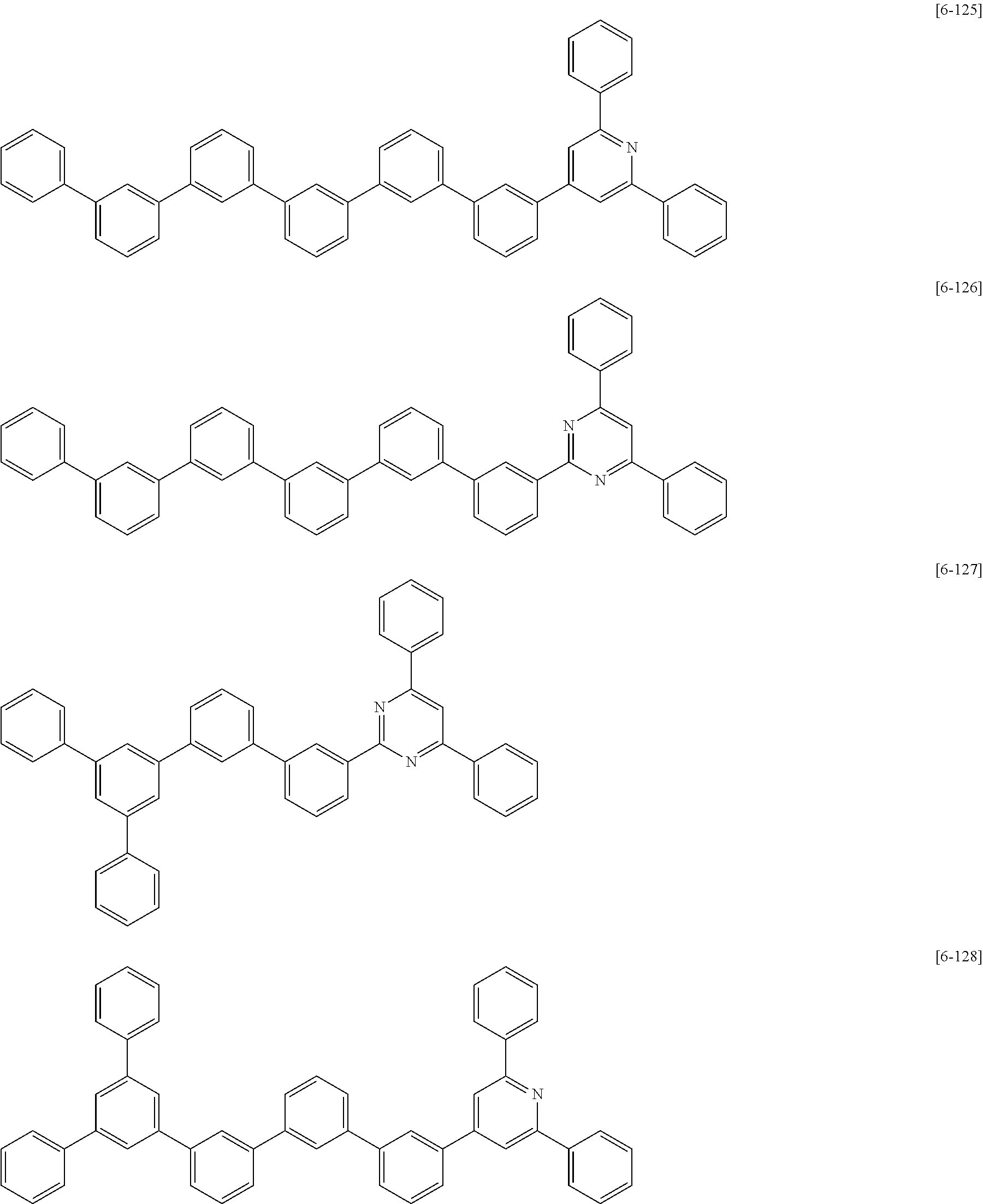


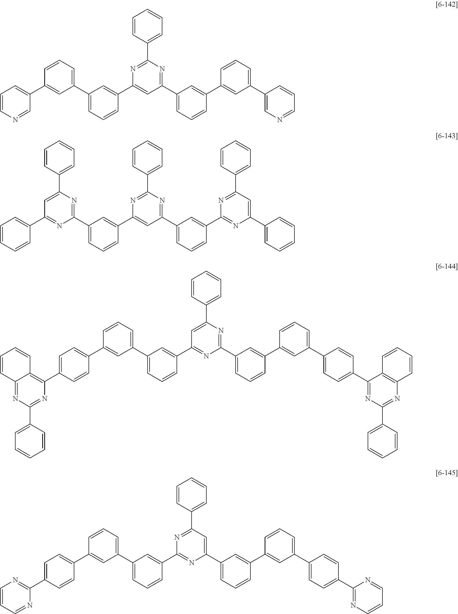


The composition may include the first compound for an organic optoelectric device and the second compound for an organic optoelectric device in a weight ratio of about 1:99 to 99:1.
The composition may be applied to an organic layer of an organic optoelectric device, and the first compound for an organic optoelectric device and the second compound for an organic optoelectric device may act as hosts.
The first compound for an organic optoelectric device may be a compound having relatively strong hole characteristics, while the second compound for an organic optoelectric device may be a compound having relatively strong electron characteristics, and thus, when the first and second compounds for an organic optoelectric device are used together, luminous efficiency and life-span characteristics may be further improved by increasing mobility and stability of charges.
The composition may further include one or more kinds of organic compounds in addition to the first compound for an organic optoelectric device and the second compound for an organic optoelectric device.
The composition may further include a dopant. The dopant may be a red, green, or blue dopant, for example a phosphorescent dopant.
The dopant is a material that is mixed with the first host compound and the second host compound in a small amount to cause light emission, and may be a material such as a metal complex that emits light by multiple excitation into a triplet or more. The dopant may be, for example an inorganic, organic, or organic/inorganic compound, and one or more kinds thereof may be used.
Examples of the dopant may be an organometal compound including Ir, Pt, Os, Ti, Zr, Hf, Eu, Tb, Tm, Fe, Co, Ni, Ru, Rh, Pd, or a combination thereof. The phosphorescent dopant may be, for example a compound represented by the following Chemical Formula Z, but is not limited thereto.
L2MX [Chemical Formula Z]
L2MX [Chemical Formula Z]
In Chemical Formula Z, M is a metal, and L and X are the same or different, and are a ligand to form a complex compound with M.
The M may be, for example Ir, Pt, Os, Ti, Zr, Hf, Eu, Tb, Tm, Fe, Co, Ni, Ru, Rh, Pd, or a combination thereof, and the L and X may be, for example a bidendate ligand.
The composition may be formed by a dry method, such as chemical vapor deposition (CVD), or a solution process.
Hereinafter, an organic optoelectric device including the compound for an organic optoelectric device or the composition is described.
The organic optoelectric device may be any device to convert electrical energy into photoenergy and vice versa without particular limitation, and may be, for example an organic photoelectric device, an organic light emitting diode, an organic solar cell, and an organic photo-conductor drum.
The organic optoelectric device includes an anode and a cathode facing each other, and at least one organic layer between the anode and the cathode, wherein the organic layer includes the compound for an organic optoelectric device or the composition for an organic optoelectric device.
Herein, an organic light emitting diode as one example of an organic optoelectric device is described referring to drawings.
Referring to FIG. 1 , an organic light emitting diode 100 according to an embodiment includes an anode 120 and a cathode 110 facing each other and an organic layer 105 interposed between the anode 120 and the cathode 110.
The anode 120 may be made of a conductor having a large work function to help hole injection, and may be, for example, metal, metal oxide and/or a conductive polymer. The anode 120 may be, for example a metal such as nickel, platinum, vanadium, chromium, copper, zinc, or gold, or an alloy thereof; a metal oxide such as zinc oxide, indium oxide, indium tin oxide (ITO), indium zinc oxide (IZO), or the like; a combination of metal and oxide such as ZnO and Al or SnO2 and Sb; a conductive polymer such as poly(3-methylthiophene), poly(3,4-(ethylene-1,2-dioxy)thiophene) (PEDT), polypyrrole, or polyaniline, but is not limited thereto.
The cathode 110 may be made of a conductor having a small work function to help electron injection, and may be, for example, metal, metal oxide, and/or a conductive polymer. The cathode 110 may be, for example, a metal or an alloy thereof such as magnesium, calcium, sodium, potassium, titanium, indium, yttrium, lithium, gadolinium, aluminum, silver, tin, lead, cesium, barium, or the like; a multi-layer structure material such as LiF/Al, LiO2/Al, LiF/Ca, LiF/Al, or BaF2/Ca, but is not limited thereto.
The organic layer 105 includes an emission layer 130 including the compound for an organic optoelectric device or the composition for an organic optoelectric device according to an embodiment.
The emission layer 130 may include, for example, the compound for an organic optoelectric device individually, a mixture of at least two of the compounds for an organic optoelectric device, or the composition for an organic optoelectric device.
In the emission layer 130, the first and second compounds for an organic optoelectric device may be included for example in a weight ratio of about 1:99 to about 99:1. The weight ratio may be about 10:90 to about 90:10, about 20:80 to about 80:20, about 30:70 to about 70:30, about 40:60 to about 60:40, and about 50:50. In addition, the first and second compounds for an organic optoelectric device may be mixed in a weight ratio of about 1:2, about 1:3, about 1:4, about 1:5, about 1:1, about 2:1, about 3:1, about 4:1, about 5:1, and the like. The mixing may be performed by first mixing two compounds and depositing the mixture, or simultaneously depositing each compound in each weight ratio.
When the compounds are included within the range, electron-injecting capability may be adjusted depending on a ratio of the two compounds and balanced with electron transport capability of the emission layer, and thus, electrons may not be accumulated on the interface of the emission layer.
The first compound for an organic optoelectric device having relatively strong hole characteristics and the second compound for an organic optoelectric device having relatively strong electron characteristics in the emission layer may be used together and may increase mobility and stability of charges.
For example, the first compound for an organic optoelectric device represented by Chemical Formula I-A or I-D or the second compound for an organic optoelectric device represented by Chemical Formula II-A or II-B may be used together. For example, the first compound for an organic optoelectric device represented by Chemical Formula Ia or Id and the second compound for an organic optoelectric device represented by Chemical Formula II-A1 or II-b1 may be used together.
Referring to FIG. 2 , an organic light emitting diode 200 further includes a hole auxiliary layer 140 in addition to an emission layer 130. The hole auxiliary layer 140 may improve hole injection and/or hole mobility between the anode 120 and the emission layer 130 and may block electrons. The hole auxiliary layer 140 may include, for example at least one of a hole transport layer, a hole injection layer, and/or an electron blocking layer.
The hole auxiliary layer 140 may include the compound for an organic optoelectric device or the composition for an organic optoelectric device. For example, the hole auxiliary layer 140 may be positioned to be adjacent to the emission layer and include the compound for an organic optoelectric device or the composition for an organic optoelectric device.
In the present specification, when at least two hole transport layers (HTL) are formed, the hole transport layer (HTL) neighboring the emission layer is called a hole transport auxiliary layer.
An organic light emitting diode according to an embodiment may further include an electron transport layer (ETL), an electron injection layer (EIL), a hole injection layer (HIL) and the like as the organic layer 105 as shown in FIG. 1 or 2 .
The organic light emitting diodes 100 and 200 may be manufactured by forming an anode or a cathode on a substrate, forming an organic layer in accordance with a dry coating method such as evaporation, sputtering, plasma plating, and ion plating; and forming a cathode or an anode thereon.
The organic light emitting diode may be applied to an organic light emitting diode (OLED) display.
The following Examples and Comparative Examples are provided in order to highlight characteristics of one or more embodiments, but it will be understood that the Examples and Comparative Examples are not to be construed as limiting the scope of the embodiments, nor are the Comparative Examples to be construed as being outside the scope of the embodiments. Further, it will be understood that the embodiments are not limited to the particular details described in the Examples and Comparative Examples.
Synthesis of Compound for Organic Optoelectric Device
Hereinafter, starting materials and reaction materials used in Examples and Synthesis Examples were purchased from Sigma-Aldrich Co. Ltd. or TCI Inc. unless particularly mentioned otherwise.


1st Step: Synthesis of Intermediate 1-1
29.98 g (127.09 mmol) of 1,3-dibromobenzene was dissolved in 500 mL of tetrahydrofuran under a nitrogen environment, and the solution was cooled down to −70° C. by using liquid nitrogen.
Next, 56 mL (139.80 mmol) of 2.5 M n-butyllithium (a hexane solvent) was slowly injected thereinto, and the mixture was agitated for 40 minutes. Then, 25 g (139.80 mmol) of 9-fluorenone dissolved in 50 mL of tetrahydrofuran was slowly injected thereinto after cooling down a reactor with liquid nitrogen. The reactor was heated up to room temperature, and then the mixture was agitated for 12 hours. When the reaction was complete, the reactant was poured into 500 mL of an ammonium chloride aqueous solution, and an organic layer was separated and then purified through column chromatography after removing a solvent therefrom, obtaining 35 g (82%) of an intermediate 1-1.
2nd Step: Synthesis of Intermediate 1-2
26.8 g (79.7 mmol) of the intermediate 1-1 was dissolved in 700 mL of benzene and then heated at 50° C. Then, 13 g (87.67 mmol) of trifluoromethanesulfonic acid was slowly injected thereto, and the mixture was agitated for 2 hours. The reactant was poured into a sodium bicarbonate aqueous solution for neutralization, and then an organic layer was separated therefrom and purified through column chromatography, obtaining 24 g (76%) of an intermediate 1-2.
3rd Step: Synthesis of Intermediate 1-3
26 g (104.9 mmol) of 3-bromocarbazole was dissolved in 400 mL of tetrahydrofuran under a nitrogen environment, 46.5 g (125.9 mmol) of 9-Phenyl-9H-carbazol-3-yl-3-boronic acid pinacol ester (Matrix Scientific) and 6.1 g (5.25 mmol) of tetrakis(triphenylphosphine)palladium were added thereto, and the mixture was agitated. Then, 43.5 g (314.75 mmol) of potassium carbonate saturated in water was added thereto, and the mixture was heated and refluxed at 80° C. for 24 hours. When the reaction was complete, water was added to the reaction solution, the mixture was extracted with dichloromethane, filtered after removing moisture with anhydrous MgSO4 therefrom and concentrated under a reduced pressure. Then, a residue obtained therefrom was separated and purified through column chromatography, obtaining 33 g (77%) of an intermediate 1-3.
4th Step: Synthesis of Compound 2-1
8.86 g (21.68 mmol) of the intermediate 1-3, 9.48 g (23.85 mmol) of the intermediate 1-2, 0.62 g (1.08 mmol) of bisdibenzylidene acetonepalladium, 2.13 g (32.52 mmol) of sodium tert-butoxide, 2.104 g (4.34 (mmol) of tri-tert-butylphosphine (50%-toluene) and 90 mL of toluene were put in a reaction vessel and agitated under a nitrogen stream at 110° C. for 12 hours. When the reaction was complete, the reaction solution was filtered and then recrystallized with toluene, obtaining 13 g (83%) of a compound 2-1.
LC Mass (calcd.: 724.89 g/mol, found: M+H+=725.69 g/mol).

1st Step: Synthesis of Intermediate 2-1
29 g (81%) of an intermediate 2-1 was obtained according to the same synthesis method as the method of preparing the intermediate 1-1 by using 25 g (105.9 mmol) of 1,4-dibromobenzene, 46.6 mL (116.5 mmol) of 2.5 M n-butyllithium (a hexane solvent) and 21 g (116.50 mmol) of 9-fluorenone.
2nd Step: Synthesis of Intermediate 2-2
25 g (75%) of an intermediate 2-2 was obtained according to the same synthesis method as the method of preparing the intermediate 1-2 by using 28.3 g (83.90 mmol) of the intermediate 2-1 and 13.8 g (92.29 mmol) of trifluoromethanesulfonic acid.
3rd Step: Synthesis of Compound 2-6
13.5 g (79%) of a compound 2-6 was obtained according to the same synthesis method as Synthesis Example 1 by using 9.66 g (23.65 mmol) of the intermediate 1-3 and 10.336 g (26.01 mmol) of the intermediate 2-2.
LC Mass (calcd.: 724.89 g/mol, found: M+H+=725.70 g/mol).


1st Step: Synthesis of Intermediate 3-1
31.2 g (73%) of an intermediate 3-1 was obtained according to the same synthesis method as the method of preparing the intermediate 1-1 by using 26 g (165.9 mmol) of bromobenzene, 73 mL (182.50 mmol) of 2.5 M n-butyllithium (a hexane solvent) and 32.8 g (182.50 mmol) of 9-fluorenone.
2nd Step: Synthesis of Intermediate 3-2
35 g (82%) of an intermediate 3-2 1 was obtained according to the same synthesis method as the method of preparing the intermediate 1-3 by using 28.5 g (88.44 mmol) of 3-bromo-9-phenylcarbazole and 45.720 g (123.8 mmol) of 9-Phenyl-9H-carbazol-3-yl-3-boronic acid pinacol ester (Matrix Scientific).
3rd Step: Synthesis of Compound 2-42
22.8 g (45.98 mmol) of the intermediate 3-2 and 11.8 g (45.98 mmol) of the intermediate 3-1 were dissolved in 450 mL of dichloromethane, and the solution was agitated at room temperature. Then, 3.2 g (22.99 mmol) of borontrifluoride (an ethyl ether complex) was slowly added thereto in a dropwise fashion. The mixture was agitated at room temperature for 2 hours, neutralized with a sodium bicarbonate aqueous solution, extracted with dichloromethane and then recrystallized with chlorobenzene, obtaining 24 g (72%) a compound 2-42.
LC Mass (calcd.: 724.89 g/mol, found: M+H+=725.71 g/mol).

[Compound a]
12.5 g (80%) of a compound a was obtained according to the same method as Synthesis Example 1 by using 10.7 g (26.16 mmol) of the intermediate 1-3 and 8.6 g (31.4 mmol) of the 2-bromo-9,9-dimethylfluorene.
LC Mass (calcd.: 600.75 g/mol, found: M+H+=601.64 g/mol).


[Compound b]
1st Step: Synthesis of Intermediate 5-1
19 g (48%) of an intermediate 5-1 was obtained according to the same method as the synthesis method of Reaction Scheme 4 by using 24.7 g (100.4 mmol) of 3-bromocarbazole and 52.261 g (200.8 mmol) of 4-iodinebiphenyl.
2nd Step: Synthesis of Intermediate 5-2
12.8 g (44.7 mmol) of the intermediate 5-1 was dissolved in 300 mL of dimethyl formamide under a nitrogen environment, 13.6 g (53.6 mmol) of bis(pinacolato)diboron, 1.825 g (2.23 mmol) of (1,1′-bis(diphenylphosphine)ferrocene)dichloropalladium (II) and 6.6 g (67 mmol) of potassium acetate were added thereto, and the mixture was heated and refluxed at 150° C. for 24 hours. When the reaction was complete, water was added to the reaction solution, and the mixture was filtered and dried in a vacuum oven. Then, a residue obtained therefrom was separated and purified through column chromatography, obtaining 14 g (70%) of the intermediate 5-2.
3rd Step: Synthesis of Intermediate 5-3
12 g (84%) of an intermediate 5-3 was obtained according to the same method as the method of synthesizing the intermediate 1-3 by using 13.1 g (29.5 mmol) of the intermediate 5-2 and 8 g (32.43 mmol) of 3-bromocarbazole.
4th Step: Synthesis of Compound b
11.3 g (72%) of a compound b was obtained according to the same method as the synthesis method of Reaction Scheme 4 by using 11.25 g (23.33 mmol) of the intermediate 5-3 and 7 g (25.54 mmol) of 2-bromo-9,9-dimethylfluorene.
LC Mass (calcd.: 676.84 g/mol, found: M+H+=677.75 g/mol).
An organic light emitting diode was manufactured by using 4,4′-di(9H-carbazol-9-yl)biphenyl (CBP) as a host and PhGD (illustrated below) as a dopant. As for an anode, a 1000 Å-thick ITO was used, while as for a cathode, a 1000 Å-thick aluminum (Al) was used. The organic light emitting diode is manufactured in a method of ultrasonic wave-cleaning an ITO glass substrate in acetone, isopropyl alcohol and pure water respectively for 15 minutes and then UV ozone cleaning it for 30 minutes. On the substrate, a 800 Å-thick hole transport layer (HTL) was formed by vacuum-depositing HT-1 to be 70 nm thick at a vacuum degree of 650×10−7 Pa and a deposition rate ranging from 0.1 to 0.3 nm/s and depositing the compound 2-1 according to Synthesis Example 1 to form a 10 nm-thick hole transport auxiliary layer. Subsequently, a 300 Å-thick emission layer was formed by depositing 4,4′-di(9H-carbazol-9-yl)biphenyl (CBP) under the same vacuum deposition condition as above and herein, simultaneously depositing PhGD of a phosphorescent dopant. Herein, the phosphorescent dopant was deposited in an amount of 7 wt % based on 100 wt % of the emission layer by adjusting the deposition rate. On the emission layer, a 50 Å-thick hole blocking layer was formed by depositing bis(2-methyl-8-quinolinolate)-4-(phenylphenolato)aluminum (BAlq) under the same vacuum deposition condition as above. Subsequently, a 200 Å-thick electron transport layer (ETL) was formed by depositing Alq3 under the same deposition condition as above. On the electron transport layer (ETL), a cathode was formed by sequentially depositing LiF and Al, finally manufacturing an organic photoelectric device. The organic photoelectric device had a structure of ITO/HT-1 (70 nm)/the compound 2-1 (10 nm)/EML (CBP (93 wt %)+PhGD (7 wt %), 30 nm)/Balq (5 nm)/Alq3 (20 nm)/LiF (1 nm)/Al (100 nm).
An organic light emitting diode was manufactured according to the same method as Example 1 except for using the compound 2-6 according to Synthesis Example 2 instead of the compound 2-1 according to Synthesis Example 1.
An organic light emitting diode was manufactured according to the same method as Example 1 except for using the compound 2-42 according to Synthesis Example 3 instead of the compound 2-1 according to Synthesis Example 1.
An organic light emitting diode was manufactured according to the same method as Example 1 except for using the compound a according to Comparative Synthesis Example 1 instead of the compound 2-1 according to Synthesis Example 1.
An organic light emitting diode was manufactured according to the same method as Example 1 except for using the compound b according to Comparative Synthesis Example 2 instead of the compound 2-1 according to Synthesis Example 1.
An organic light emitting diode was manufactured according to the same method as Example 1 except for using HT-1 instead of the compound 2-1 according to Synthesis Example 1.
The structures of the HT-1, BAlq, CBP, and PhGD used for manufacturing the organic light emitting diode were as follows.

Evaluation
Current density and luminance changes depending on a voltage, luminous efficiency and life-span of each organic light emitting diode according to Examples 1 to 3 and Comparative Examples 1 to 3 were measured.
Specific measurement methods were as follows, and the results were provided in Table 1.
(1) Measurement of Current Density Change Depending on Voltage Change
The obtained organic light emitting diodes were measured for current value flowing in the unit device while increasing the voltage from 0 V to 10 V using a current-voltage meter (Keithley 2400), the measured current value was divided by area to provide the results.
(2) Measurement of Luminance Change Depending on Voltage Change
Luminance was measured by using a luminance meter (Minolta Cs-1000A), while the voltage of the organic light emitting diodes was increased from 0 V to 10 V.
(3) Measurement of Luminous Efficiency
Current efficiency (cd/A) at the same current density (10 mA/cm2) were calculated by using the luminance, current density, and voltages (V) from the items (1) and (2).
(4) Life-span
The T90 life-span result was obtained by maintaining luminance (cd/m2) of 3000 cd/m2 and measuring time taken until current efficiency (cd/A) decreased down to 90%.
| TABLE 1 | ||||
| T90 life- | ||||
| Color | span (h) | |||
| Hole transport layer | (EL | Efficiency | At 3000 | |
| Nos. | (HTL) | color) | (cd/A) | cd/m2 |
| Example 1 | HT-1/compound 2-1 | Green | 42.3 | 230 |
| Example 2 | HT-1/compound 2-6 | Green | 40.7 | 225 |
| Example 3 | HT-1/compound 2-42 | Green | 40.2 | 223 |
| Comparative | HT-1/compound a | Green | 36.8 | 185 |
| Example 1 | ||||
| Comparative | HT-1/compound b | Green | 37.5 | 190 |
| Example 2 | ||||
| Comparative | HT-1/HT-1 | Green | 35.2 | 180 |
| Example 3 | ||||
Referring to the results of Table 1, Examples 1 to 3 using the compound according to an embodiment for a hole transport auxiliary layer showed improved luminous efficiency and life-span in a green phosphorescent organic light emitting diode compared with Comparative Example 3 using no hole transport auxiliary layer. In particular, an example embodiment showed at least greater than or equal to about 10% much improved luminous efficiency.
Analysis
The deposition process temperature and the glass transition temperature (Tg) of the compounds according to Synthesis Examples 1 to 3 and Comparative Synthesis Examples 1 to 2 were measured.
The temperatures were specifically measured in the following method, and the results are provided in Table 2.
Deposition Process Temperature (° C.)
The deposition process temperature indicates a temperature at which a compound for a hole transport auxiliary layer was deposited to be 1 Å thick per 1 second (Å/sec) during the manufacture of the organic light emitting diode of Synthesis Example 1.
Glass Transition Temperature (Tg)
An energy input difference was measured as a function of a temperature by using a DSC1 equipment made by Mettler Toledo International Inc., while temperature of a sample and a reference was changed.
| TABLE 2 | |||
| Molecular | Deposition temperature | Tg | |
| Nos. | weight | (° C.) | (° C.) |
| Synthesis Example 1 | 724.89 | 220 | 149 |
| Synthesis Example 2 | 724.89 | 230 | 161 |
| Synthesis Example 3 | 724.89 | 231 | 172 |
| Comparative | 600.75 | 223 | 132 |
| Synthesis Example 1 | |||
| Comparative | 676.84 | 238 | 146 |
| Synthesis Example 2 | |||
Referring to Table 2, the compounds according to an embodiment showed a similar or the same deposition process temperature to or as those of the compounds according to Comparative Synthesis Examples 1 to 2 as an absolute value but a lower process temperature based on their molecular weight. In other words, the compounds having a low process temperature based on their molecular weight had a very commercially advantageous condition when used to manufacture an organic light emitting diode. Without being bound by theory, this is believed to be because the compound had non-planarity due to a phenyl group substituted at No. 9 of fluorine and thus, was suppressed from an interaction among molecules. In addition, the compounds according to an embodiment had a higher glass transition temperature than the compounds according to Comparative Synthesis Examples 1 and 2. Without being bound by theory, it is believed that the compounds having a high glass transition temperature prevented degradation of a device due to Joule's heat during the operation and realized a device having a stable long life-span.
Luminous efficiency and life-span are significant factors in terms of commercialization of a device. Based on the results of Examples, the results of the Examples are sufficient to commercialize the device. In addition, the compounds had a low process temperature and thus, decreased time for manufacturing the device and also, had a high glass transition temperature and contributed to realizing a device having a stable long life-span.
A compound 4-10 was synthesized through the following synthesis method and the like.
1st Step: Synthesis of Intermediate 1-2

32.7 g (107 mmol) of 2-bromotriphenylene was dissolved in 300 ml of tetrahydrofuran under a nitrogen environment, 20 g (128 mmol) of 3-chlorophenylboronic acid and 1.23 g (1.07 mmol) of tetrakis(triphenylphosphine)palladium were added thereto, and the mixture was agitated. Then, 36.8 g (267 mmol) of potassium carbonate saturated in water was heated and refluxed at 80° C. for 24 hours. When the reaction was complete, water was added to the reaction solution, and the mixture was extracted with dichloromethane and then filtered after removing moisture with anhydrous MgSO4 and concentrated under a reduced pressure. Then, a residue obtained therefrom was separated and purified through column chromatography, obtaining 22.6 g (63%) of the compound I-2.
2nd Step: Synthesis of Intermediate I-3

22.6 g (66.7 mmol) of the compound I-2 was dissolved in 300 ml of dimethyl formamide under a nitrogen environment, 25.4 g (100 mmol) of bis(pinacolato)diboron, 0.54 g (0.67 mmol) of (1,1′-bis(diphenylphosphine)ferrocene)dichloropalladium (II) and 16.4 g (167 mmol) of potassium acetate were added thereto, and the mixture was heated and refluxed at 150° C. for 48 hours. When the reaction was complete, water was added to the reaction solution, the mixture was filtered and then dried in a vacuum oven. Then, a residue obtained therefrom was separated and purified through column chromatography, obtaining 18.6 g (65%) of a compound I-3.
3rd Step: Synthesis of Intermediate I-6

50 g (116 mmol) of the compound I-3 was dissolved in 500 ml of tetrahydrofuran under a nitrogen environment, 39.4 g (139 mmol) of 1-bromo-3-iodobenzene and 1.34 g (1.16 mmol) of tetrakis(triphenylphosphine)palladium were added thereto, and the mixture was agitated. Then, 40.1 g (290 mmol) of potassium carbonate saturated in water was added thereto, and the mixture was heated and refluxed at 80° C. for 12 hours. When the reaction was complete, water was added to the reaction solution, and the mixture was extracted with dichloromethane and then filtered after removing moisture with anhydrous MgSO4 and concentrated under a reduced pressure. Then, a residue obtained therefrom was separated and purified through column chromatography, obtaining 42.6 g (80%) of a compound I-6.
4th Step: Synthesis of Intermediate I-7

40 g (87.1 mmol) of the compound I-6 was dissolved in 300 ml of dimethyl formamide under a nitrogen environment, 26.5 g (104 mmol) of bis(pinacolato)diboron, 0.71 g (0.87 mmol) of (1,1′-bis(diphenylphosphine)ferrocene)dichloropalladium (II), and 21.4 g (218 mmol) of potassium acetate were added thereto, and the mixture was heated and refluxed at 150° C. for 26 hours. When the reaction was complete, water was added to the reaction solution, and the mixture was filtered and dried in a vacuum oven. Then, a residue obtained therefrom was separated and filtered through column chromatography, obtaining 34 g (77%) of the compound I-7.
5th Step: Synthesis of Compound 4-10

20 g (39.5 mmol) of the compound 1-7 was dissolved in 200 ml of tetrahydrofuran under a nitrogen environment, 10.6 g (39.5 mmol) of 2-chloro-4,6-diphenyl-1,3,5-triazine and 0.46 g (0.4 mmol) of tetrakis(triphenylphosphine)palladium were added thereto, and the mixture was agitated. Then, 13.6 g (98.8 mmol) of potassium carbonate saturated in water was heated and refluxed at 80° C. for 23 hours. When the reaction was complete, water was added to the reaction solution, and the mixture was extracted with dichloromethane and then filtered after removing moisture with anhydrous MgSO4 and concentrated under a reduced pressure. Then, a residue obtained therefrom was separated and purified through column chromatography, obtaining 17.9 g (74%) of the compound 4-10.
LC Mass (calcd.: 611.73 g/mol, found: M+H+=612.54 g/mol).
A compound 6-1 was synthesized through the following synthesis method.
1st Step: Synthesis of Intermediate II-1

50 g (187 mmol) of the compound, 2-chloro-4,6-diphenyl-1,3,5-triazine was dissolved in 1 L of THF (tetrahydrofuran) under a nitrogen environment, 45 g (224.12 mmol) of (3-bromophenyl)boronic acid and 2.1 g (1.87 mmol) of tetrakis(triphenylphosphine)palladium were added thereto, and the mixture was agitated. Then, 64 g (467 mmol) of potassium carbonate saturated in water was added thereto, and the resulting mixture was heated and refluxed at 80° C. for 12 hours. When the reaction was complete, water was added to the reaction solution, and the mixture was extracted with dichloromethane (DCM) and then filtered after removing moisture with anhydrous MgSO4 and concentrated under a reduced pressure. Then, the obtained residue was separated and purified through flash column chromatography, obtaining 69 g (95%) of the compound II-1.
Synthesis of Intermediate II-2

50 g (128 mmol) of the compound II-1 was dissolved in 1 L of THF under a nitrogen environment, 24 g (155 mmol) of (3-chlorophenyl)boronic acid and 1.5 g (1.3 mmol) of tetrakis(triphenylphosphine)palladium were added thereto, and the mixture was agitated. Then, 44 g (320 mmol) of potassium carbonate saturated in water was added thereto, and the resulting mixture was heated and refluxed at 80° C. for 12 hours. When the reaction was complete, water was added to the reaction solution, and the mixture was extracted with dichloromethane (DCM) and then filtered after removing moisture with anhydrous MgSO4 and concentrated under a reduced pressure. Then, the obtained residue was separated and purified through flash column chromatography, obtaining 51 g (95%) of the compound II-2.
3rd Step: Synthesis of Intermediate II-3

100 g (238 mmol) of the compound II-2 was dissolved in 1 L of dimethylformamide (DMF) under a nitrogen environment, 72.5 g (285 mmol) of bis(pinacolato)diboron, 2 g (2.38 mmol) of (1,1′-bis(diphenylphosphine)ferrocene)dichloropalladium (II) and 58 g (595 mmol) of potassium acetate were added thereto, and the mixture was heated and refluxed at 150° C. for 48 hours. When the reaction was complete, water was added to the reaction solution, and the mixture was filtered and dried in a vacuum oven. The obtained residue was separated and purified through flash column chromatography, obtaining 107 g (88%) of the compound II-3.
4th Step: Synthesis of Intermediate II-4

50 g (98 mmol) of the compound II-3 was dissolved in 1 L of THF under a nitrogen environment, 33 g (117 mmol) of 1-bromo-3-iodobenzene and 1 g (0.98 mmol) of tetrakis(triphenylphosphine)palladium were added thereto, and the mixture was agitated. Then, 34 g (245 mmol) of potassium carbonate saturated in water was added thereto, and the mixture was heated and refluxed at 80° C. for 12 hours. When the reaction was complete, water was added to the reaction solution, and the mixture was extracted with dichloromethane (DCM) and then filtered after removing moisture with anhydrous MgSO4 and concentrated under a reduced pressure. The obtained residue was separated and purified through flash column chromatography, obtaining 50 g (95%) of the compound II-4.
5th Step: Synthesis of Intermediate II-5

100 g (185 mmol) of the compound II-4 was dissolved in 1 L of dimethylformamide (DMF) under a nitrogen environment, 56 g (222 mmol) of bis(pinacolato)diboron, 1.5 g (1.85 mmol) of (1,1′-bis(diphenylphosphine)ferrocene)dichloropalladium (II) and 45 g (595 mmol) of potassium acetate were added thereto, and the mixture was heated and refluxed at 150° C. for 5 hours. When the reaction was complete, water was added to the reaction solution, and the mixture was filtered and dried in a vacuum oven. The obtained residue was separated and purified through flash column chromatography, obtaining 95 g (88%) of the compound II-5.
6th Step: Synthesis of Compound 6-1

20 g (34 mmol) of the compound II-5 was dissolved in 0.2 L of tetrahydrofuran (THF) under a nitrogen environment, 9.5 g (40 mmol) of 3-bromo-1,1′-biphenyl and 0.39 g (0.34 mmol) of tetrakis(triphenylphosphine)palladium were added thereto, and the mixture was agitated. Then, 12 g (85 mmol) of potassium carbonate saturated in water was added thereto, and the mixture was heated and refluxed at 80° C. for 20 hours. When the reaction was complete, water was added to the reaction solution, and the mixture was extracted with dichloromethane (DCM) and then filtered after removing moisture with anhydrous MgSO4 and concentrated under a reduced pressure. The obtained residue was separated and purified through flash column chromatography, obtaining 24 g (70%) of the compound 6-1.
LC Mass (calcd.: 613.75 g/mol, found: M+H+=614.62 g/mol).

20 g (39.1 mmol) of the compound II-3 was dissolved in 0.2 L of tetrahydrofuran (THF) under a nitrogen environment, 14.5 g (47 mmol) of 5″-bromo-1,1′:3′,1″-terphenyl and 0.45 g (0.39 mmol) of tetrakis(triphenylphosphine)palladium were added thereto, and the mixture was agitated. Then, 9.7 g (99 mmol) of potassium carbonate saturated in water was added thereto, and the resulting mixture was heated and refluxed at 80° C. for 20 hours. When the reaction was complete, water was added to the reaction solution, and the mixture was extracted with dichloromethane (DCM) and then filtered after removing moisture with anhydrous MgSO4 and concentrated under a reduced pressure. The obtained residue was separated and purified through flash column chromatography, obtaining 20 g (83%) of the compound 6-5.
LC Mass (calcd.: 613.75 g/mol, found: M+H+=614.63 g/mol).

20 g (34 mmol) of the compound II-5 was dissolved in 0.2 L of tetrahydrofuran (THF) under a nitrogen environment, 12.6 g (40 mmol) of 5′-bromo-1,1′:3′,1″-terphenyl and 0.40 g (0.34 mmol) of tetrakis(triphenylphosphine)palladium were added thereto, and the mixture was agitated. Then, 12 g (85 mmol) of potassium carbonate saturated in water was heated and refluxed at 80° C. for 20 hours. When the reaction was complete, water was added to the reaction solution, and the mixture was extracted with dichloromethane (DCM) and then filtered after removing moisture with anhydrous MgSO4 and concentrated under a reduced pressure. The obtained residue was separated and purified through flash column chromatography, obtaining 19 g (80%) of the compound 6-7.
LC Mass (calcd.: 689.84 g/mol, found: M+H+=690.72 g/mol).
1st Step: Synthesis of Intermediate I-17

50 g (187 mmol) of the compound, 2-chloro-4,6-diphenylpyrimidine was dissolved in 1 L of THF under a nitrogen environment, 37 g (155 mmol) of (3-bromophenyl)boronic acid and 2.1 g (1.8 mmol) of tetrakis(triphenylphosphine)palladium were added thereto, and the mixture was agitated. Then, 64 g (467 mmol) of potassium carbonate saturated in water was added thereto, and the resulting mixture was heated and refluxed at 80° C. for 12 hours. When the reaction was complete, water was added to the reaction solution, and the mixture was extracted with dichloromethane (DCM) and then filtered after removing moisture with anhydrous MgSO4 and concentrated under a reduced pressure. The obtained residue was separated and purified through flash column chromatography, obtaining 66 g (92%) of the compound I-17.
2nd Step: Synthesis of Intermediate I-18

50 g (129 mmol) of the compound I-17 was dissolved in 1 L of THF under a nitrogen environment, 24 g (155 mmol) of (3-chlorophenyl)boronic acid and 1.5 g (1.3 mmol) of tetrakis(triphenylphosphine)palladium were added thereto, and the mixture was agitated. Then, 45 g (322 mmol) of potassium carbonate was added thereto, and the mixture was heated and refluxed at 80° C. for 12 hours. When the reaction was complete, water was added to the reaction solution, and the mixture was extracted with dichloromethane (DCM) and then filtered after removing moisture with anhydrous MgSO4 and concentrated under a reduced pressure. The obtained residue was separated and purified through flash column chromatography, obtaining 50 g (92%) of the compound I-18.
3rd Step: Synthesis of Intermediate I-19

100 g (239 mmol) of the compound I-18 was dissolved in 1 L of dimethylformamide (DMF) under a nitrogen environment, 72.5 g (287 mmol) of bis(pinacolato)diboron, 2 g (2.38 mmol) of (1,1′-bis(diphenylphosphine)ferrocene)dichloropalladium (II) and 58 g (595 mmol) of potassium acetate were added thereto, and the mixture was heated and refluxed at 150° C. for 48 hours. When the reaction was complete, water was added to the reaction solution, and the mixture was filtered and dried in a vacuum oven. The obtained residue was separated and purified through flash column chromatography, obtaining 105 g (86%) of the compound I-19.
4th Step: Synthesis of Intermediate I-20

50 g (98 mmol) of the compound I-19 was dissolved in 1 L of THF under a nitrogen environment, 33 g (117 mmol) of 1-bromo-3-iodobenzene and 1 g (0.98 mmol) of tetrakis(triphenylphosphine)palladium were added thereto, and the mixture was agitated. Then, 34 g (245 mmol) of potassium carbonate saturated in water was heated and refluxed at 80° C. for 12 hours. When the reaction was complete, water was added to the reaction solution, and the mixture was extracted with dichloromethane (DCM) and then filtered after removing moisture with anhydrous MgSO4 and concentrated under a reduced pressure. The obtained residue was separated and purified through flash column chromatography, obtaining 50 g (95%) of the compound I-20.
5th Step: Synthesis of Intermediate I-21

100 g (185 mmol) of the compound I-20 was dissolved in 1 L of dimethylformamide (DMF) under a nitrogen environment, 56 g (222 mmol) of bis(pinacolato)diboron, 1.5 g (1.86 mmol) of (1,1′-bis(diphenylphosphine)ferrocene)dichloropalladium (II) and 58 g (595 mmol) of potassium acetate were added thereto, and the mixture was heated and refluxed at 150° C. for 12 hours. When the reaction was complete, water was added to the reaction solution, and the mixture was filtered and dried in a vacuum oven. The obtained residue was separated and purified through flash column chromatography, obtaining 61 g (89%) of the compound I-21.
6th Step: Synthesis of Compound 6-90

20 g (34 mmol) of the compound I-21 was dissolved in 0.2 L of tetrahydrofuran (THF) in a nitrogen environment, 9.5 g (40 mmol) of 3-bromo-1,1′-biphenyl and 0.39 g (0.34 mmol) of tetrakis(triphenylphosphine)palladium were added thereto, and the mixture was agitated. Then, 12 g (85 mmol) of potassium carbonate was added thereto, and the resulting mixture was heated and refluxed at 80° C. for 20 hours. When the reaction was complete, water was added to the reaction solution, and the mixture was extracted with dichloromethane (DCM) and then filtered after removing moisture with anhydrous MgSO4 and concentrated under a reduced pressure. The obtained residue was separated and purified through flash column chromatography, obtaining 16 g (75%) of the compound 6-90.
LC Mass (calcd.: 612.76 g/mol, found: M+H+=613.68 g/mol).
1st Step: Synthesis of Intermediate I-10

50 g (98 mmol) of the compound II-3 was dissolved in 1 L of THF under a nitrogen environment, 33 g (117 mmol) of 1-bromo-4-iodobenzene and 1 g (0.98 mmol) of tetrakis(triphenylphosphine)palladium were added thereto, and the mixture was agitated. Then, 34 g (245 mmol) of potassium carbonate saturated in water was added thereto, and the resulting mixture was heated and refluxed at 80° C. for 12 hours. When the reaction was complete, water was added to the reaction solution, and the mixture was extracted with dichloromethane (DCM) and then filtered after removing moisture with anhydrous MgSO4 and concentrated under a reduced pressure. The obtained residue was separated and purified through flash column chromatography, obtaining 50 g (95%) of the compound I-10.
2nd Step: Synthesis of Intermediate I-11

100 g (185 mmol) of the compound I-10 was dissolved in 1 L of dimethylformamide (DMF) under a nitrogen environment, 56 g (222 mmol) of bis(pinacolato)diboron, 1.5 g (1.85 mmol) of (1,1′-bis(diphenylphosphine)ferrocene)dichloropalladium (II) and 45 g (595 mmol) of potassium acetate were added thereto, and the mixture was heated and refluxed at 50° C. for 5 hours. When the reaction was complete, water was added to the reaction solution, and the mixture was filtered and dried in a vacuum oven. The obtained residue was separated and purified through flash column chromatography, obtaining 95 g (88%) of the compound I-11.
3rd Step: Synthesis of Compound 6-9

20 g (34 mmol) of the compound I-11 was dissolved in 0.2 L of tetrahydrofuran (THF) under a nitrogen environment, 12.6 g (40 mmol) of 5′-bromo-1,1′:3′,1″-terphenyl and 0.40 g (0.34 mmol) of tetrakis(triphenylphosphine)palladium were added thereto, and the mixture was agitated. Then, 12 g (85 mmol) of potassium carbonate saturated in water was heated and refluxed at 80° C. for 20 hours. When the reaction was complete, water was added to the reaction solution, and the mixture was extracted with dichloromethane (DCM) and then filtered and concentrated under a reduced pressure after removing moisture with anhydrous MgSO4. The obtained residue was separated and purified through flash column chromatography, obtaining 20 g (85%) of the compound 6-9.
LC Mass (calcd.: 689.84 g/mol, found: M+H+=690.71 g/mol).
A glass substrate coated with ITO (indium tin oxide) to be 1500 Å thick was ultrasonic wave-washed with a distilled water. Subsequently, the glass substrate was ultrasonic wave-washed with a solvent such as isopropyl alcohol, acetone, methanol, and the like, moved to a plasma cleaner, cleaned by using oxygen plasma for 10 minutes, and then moved to a vacuum depositor. This ITO transparent electrode was used as an anode, a 700 Å-thick hole injection layer (HIL) was formed by vacuum-depositing the compound A on the ITO substrate, and a hole transport layer (HTL) was formed by depositing the compound B to be 50 Å thick on the injection layer and the compound C to be 1020 Å thick. On the hole transport layer (HTL), a 400 Å-thick emission layer was formed by vacuum-depositing both the compound 2-1 according to Synthesis Example 1 and the compound 4-10 according to Synthesis Example 4 as a host doped with 10 wt % of tris(2-phenylpyridine)iridium (III) [Ir(ppy)3]. Herein, the compound 2-1 and the compound 4-10 were used in a ratio of 1:1.
Subsequently, on the emission layer, a 300 Å-thick electron transport layer (ETL) were formed by simultaneously vacuum-depositing the compound D and Liq in a ratio of 1:1, and a cathode was formed by sequentially vacuum-depositing Liq to be 15 Å thick and Al to be 1200 Å thick on the electron transport layer (ETL), manufacturing an organic light emitting diode.
The organic light emitting diode had a five-layered organic thin film structure specifically as follows.
A structure of ITO/compound A 700 Å/compound B 50 Å/compound C 1020 Å/EML [compound 2-1: compound 4-10:Ir(ppy)3=X:X:10%]400 Å/compound D:Liq 300 Å/Liq 15 Å/Al 1200 Å. (X=a weight ratio)
The compound A: N4,N4′-diphenyl-N4,N4′-bis (9-phenyl-9H-carbazol-3-yl)biphenyl-4,4′-diamine
The compound B: 1,4,5,8,9,11-hexaazatriphenylene-hexacarbonitrile (HAT-CN),
The compound C: N-(biphenyl-4-yl)-9,9-dimethyl-N-(4-(9-phenyl-9H-carbazol-3-yl)phenyl)-9H-fluoren-2-amine
The compound D: 8-(4-(4,6-di(naphthalen-2-yl)-1,3,5-triazin-2-yl)phenyl)quinoline
An organic light emitting diode was manufactured according to the same method as Example 4 except for using the compound 2-1 of Synthesis Example 1 and the compound 6-1 of Synthesis Example 5 in a ratio of 1:1.
An organic light emitting diode was manufactured according to the same method as Example 4 except for using the compound 2-1 of Synthesis Example 1 and the compound 6-5 of Synthesis Example 6 in a ratio of 1:1.
An organic light emitting diode was manufactured according to the same method as Example 4 except for using the compound 2-1 of Synthesis Example 1 and the compound 6-7 of Synthesis Example 7 in a ratio of 1:1.
An organic light emitting diode was manufactured according to the same method as
Example 4 except for using the compound 2-1 of Synthesis Example 1 and the compound 6-90 of Synthesis Example 8 in a ratio of 1:1.
An organic light emitting diode was manufactured according to the same method as Example 4 except for using the compound 2-6 of Synthesis Example 2 and the compound 4-10 of Synthesis Example 4 in a ratio of 1:1.
An organic light emitting diode was manufactured according to the same method as Example 4 except for using the compound 2-6 of Synthesis Example 2 and the compound 6-5 of Synthesis Example 6 in a ratio of 1:1.
An organic light emitting diode was manufactured according to the same method as Example 4 except for using the compound 2-42 of Synthesis Example 3 and the compound 4-10 of Synthesis Example 4 in a ratio of 1:1.
An organic light emitting diode was manufactured according to the same method as Example 4 except for using the compound 2-42 of Synthesis Example 3 and the compound 6-1 of Synthesis Example 5 in a ratio of 1:1.
An organic light emitting diode was manufactured according to the same method as Example 4 except for using the compound 2-42 of Synthesis Example 3 and the compound 6-5 of Synthesis Example 6 in a ratio of 1:1.
An organic light emitting diode was manufactured according to the same method as Example 4 except for using CBP as a single host instead of two hosts of the compounds according to Synthesis Examples 1 and 4.
An organic light emitting diode was manufactured according to the same method as Example 4 except for using the compound 2-1 according to Synthesis Example 1 instead of the two hosts of the compounds according to Synthesis Examples 1 and 4.
An organic light emitting diode was manufactured according to the same method as Example 4 except for using the compound 6-7 according to Synthesis Example 7 instead of the two hosts of the compounds according to Synthesis Examples 1 and 4.
Evaluation
Luminous efficiency and life-span characteristics of each organic light emitting diode according to Examples 4 to 13 and Comparative Example 4, Reference Examples 1 and 2 were measured.
Specific measurement methods were as follows, and the results are provided in Table 3.
(1) Measurement of Current Density Change Depending on Voltage Change
The obtained organic light emitting diodes were measured for current value flowing in the unit device while increasing the voltage from 0 V to 10 V using a current-voltage meter (Keithley 2400), the measured current value was divided by area to provide the results.
(2) Measurement of Luminance Change Depending on Voltage Change
Luminance was measured by using a luminance meter (Minolta Cs-1000A), while the voltage of the organic light emitting diodes was increased from 0 V to 10 V.
(3) Measurement of Luminous Efficiency
Current efficiency (cd/A) at the same current density (10 mA/cm2) were calculated by using the luminance, current density, and voltages (V) from the items (1) and (2).
(4) Life-Span
The life span result was obtained by measuring time taken until current efficiency (cd/A) decreased down to 97%, while the luminance (cd/m2) was maintained at 6000 cd/m2.
| TABLE 3 | ||||||
| First | Luminous | Life-span | ||||
| host:Sec- | efficiency | T97 | ||||
| First host | Second host | ond host | (cd/A) | (h) | ||
| Ex. 4 | Synth. Ex. 1 | Synth. Ex. 4 | 1:1 | 47.0 | 76 |
| (cmpd 2-1) | (cmpd 4-10) | ||||
| Ex. 5 | Synth. Ex. 1 | Synth. Ex. 5 | 1:1 | 46.5 | 80 |
| (cmpd 2-1) | (cmpd 6-1) | ||||
| Ex. 6 | Synth. Ex. 1 | Synth. Ex. 6 | 1:1 | 46.8 | 65 |
| (cmpd 2-1) | (cmpd 6-5) | ||||
| Ex. 7 | Synth. Ex. 1 | Synth. Ex. 7 | 1:1 | 45.5 | 68 |
| (cmpd 2-1) | (cmpd 6-7) | ||||
| Ex. 8 | Synth. Ex. 1 | Synth. Ex. 8 | 1:1 | 46.9 | 60 |
| (cmpd 2-1) | (cmpd 6-90) | ||||
| Ex. 9 | Synth. Ex. 2 | Synth. Ex. 4 | 1:1 | 46.8 | 72 |
| (cmpd 2-6) | (cmpd 4-10) | ||||
| Ex. 10 | Synth. Ex. 2 | Synth. Ex. 6 | 1:1 | 45.4 | 61 |
| (cmpd 2-6) | (cmpd 6-5) | ||||
| Ex. 11 | Synth. Ex. 3 | Synth. Ex. 4 | 1:1 | 46.6 | 67 |
| (cmpd 2-42) | (cmpd 4-10) | ||||
| Ex. 12 | Synth. Ex. 3 | Synth. Ex. 5 | 1:1 | 46.1 | 70 |
| (cmpd 2-42) | (cmpd 6-1) | ||||
| Ex. 13 | Synth. Ex. 3 | Synth. Ex. 6 | 1:1 | 46.3 | 69 |
| (cmpd 2-42) | (cmpd 6-5) |
| Comp. | CBP | — | 31.5 | 0.5 |
| Ex. 4 | ||||
| Ref. | Synth. Ex. 1 (cmpd 2-1) | — | 3.5 | 1 |
| Ex. 1 | ||||
| Ref. | Synth. Ex. 7 (cmpd 6-7) | — | 34.6 | 48 |
| Ex. 2 | ||||
Referring to Table 3, the organic light emitting diodes according to Examples 4 to 13 showed remarkably improved luminous efficiency and life-span characteristics compared with the organic light emitting diodes according to Comparative Example 4 and Reference Examples 1 and 2.
By way of summation and review, examples of an organic optoelectric device may be an organic photoelectric device, an organic light emitting diode, an organic solar cell, and an organic photo conductor drum.
Of these, an organic light emitting diode (OLED) has drawn attention due to demand for flat panel displays. Such an organic light emitting diode converts electrical energy into light by applying current to an organic light emitting material. It has a structure in which an organic layer is interposed between an anode and a cathode. Herein, an organic layer may include an emission layer and optionally an auxiliary layer, and the auxiliary layer may include, for example at least one selected from a hole injection layer, a hole transport layer, an electron blocking layer, an electron transport layer, an electron injection layer, and a hole blocking layer in order increase efficiency and stability of an organic light emitting diode.
Performance of an organic light emitting diode may be affected by characteristics of the organic layer, and among them, may be significantly affected by characteristics of an organic material of the organic layer.
For example, development for an organic material capable of increasing hole and electron mobility and simultaneously increasing electrochemical stability may be important in the case that the organic light emitting diode is applied to a large-size flat panel display.
As described above, embodiments may provide a compound for an organic optoelectric device realizing an organic optoelectric device having high efficiency and long life-span.
As described above, embodiments may provide a composition for an organic optoelectric device including the compound for an organic optoelectric device.
As described above, embodiments may provide an organic optoelectric device including the compound for an organic optoelectric device.
As described above, embodiments may provide a display device including the organic optoelectric device.
According to embodiments, an organic optoelectric device having high efficiency and long life-span may be realized.
Example embodiments have been disclosed herein, and although specific terms are employed, they are used and are to be interpreted in a generic and descriptive sense only and not for purpose of limitation. In some instances, as would be apparent to one of ordinary skill in the art as of the filing of the present application, features, characteristics, and/or elements described in connection with a particular embodiment may be used singly or in combination with features, characteristics, and/or elements described in connection with other embodiments unless otherwise specifically indicated. Accordingly, it will be understood by those of skill in the art that various changes in form and details may be made without departing from the spirit and scope of the present invention as set forth in the following claims.
-
- 100, 200: organic light emitting diode
- 105: organic layer
- 110: cathode
- 120: anode
- 130: emission layer
- 140: hole auxiliary layer
Claims (19)
1. A compound for an organic optoelectric device, the compound represented by a combination of Chemical Formula I-1 and Chemical Formula I-2 linked together:

wherein, in Chemical Formulae I-1 and I-2,
Y1 to Y8 are independently C or CRa,
W1 is N or NRb,
one of Y1 to Y8 and W1 of Chemical Formula I-2 is linked to L1 of Chemical Formula I-1,
R1 to R12, Ra and Rb are each independently hydrogen, deuterium, a substituted or unsubstituted C1 to C30 alkyl group, a substituted or unsubstituted C6 to C30 aryl group, or a combination thereof,
L1 is a single bond, a substituted or unsubstituted C6 to C30 arylene group, or a combination thereof, and
n1 is an integer of 1 to 3,
wherein “substituted” refers to that at least one hydrogen is replaced by deuterium, a halogen, a hydroxyl group, an amino group, a C1 to C30 amine group, a nitro group, a C1 to C40 silyl group, a C1 to C30 alkyl group, a C1 to C10 alkylsilyl group, a C6 to C30 arylsilyl group, a C3 to C30 cycloalkyl group, a C2 to C30 heterocycloalkyl group, a C6 to C30 aryl group, a C1 to C20 alkoxy group, a fluoro group, a C1 to C10 trifluoroalkyl group, or a cyano group.
2. The compound for an organic optoelectric device as claimed in claim 1 , wherein the compound is represented by Chemical Formulae I-A to I-E:


wherein, in Chemical Formulae I-A to I-E,
R1 to R12 and Rb are each independently hydrogen, deuterium, a substituted or unsubstituted C1 to C30 alkyl group, a substituted or unsubstituted C6 to C30 aryl group, or a combination thereof,
L1 is a single bond, a substituted or unsubstituted C6 to C30 arylene group, or a combination thereof, and
n1 is an integer of 1 to 3,
wherein “substituted” refers to that at least one hydrogen is replaced by deuterium, a halogen, a hydroxyl group, an amino group, a C1 to C30 amine group, a nitro group, a C1 to C40 silyl group, a C1 to C30 alkyl group, a C1 to C10 alkylsilyl group, a C6 to C30 arylsilyl group, a C3 to C30 cycloalkyl group, a C2 to C30 heterocycloalkyl group, a C6 to C30 aryl group, a C1 to C20 alkoxy group, a fluoro group, a C1 to C10 trifluoroalkyl group, or a cyano group.
3. The compound for an organic optoelectric device as claimed in claim 1 , wherein the Chemical Formula I-2 is represented by one of Chemical Formulae I-2a to I-2h:


wherein, in Chemical Formulae I-2a to I-2h,
Y1 to Y8 are independently C or CRa,
W1 is N or NRb,
one of Y1 to Y8 and W1 is linked to L1 of Chemical Formula I-1,
R6 to R12, Ra and Rb are each independently hydrogen, deuterium, a substituted or unsubstituted C1 to C30 alkyl group, a substituted or unsubstituted C6 to C30 aryl group, or a combination thereof, and
wherein “substituted” refers to that at least one hydrogen is replaced by deuterium, a halogen, a hydroxyl group, an amino group, a C1 to C30 amine group, a nitro group, a C1 to C40 silyl group, a C1 to C30 alkyl group, a C1 to C10 alkylsilyl group, a C6 to C30 arylsilyl group, a C3 to C30 cycloalkyl group, a C2 to C30 heterocycloalkyl group, a C6 to C30 aryl group, a C1 to C20 alkoxy group, a fluoro group, a C1 to C10 trifluoroalkyl group, or a cyano group.
4. The compound for an organic optoelectric device as claimed in claim 1 , wherein the compound is represented by Chemical Formulae I a to I e:


wherein, in Chemical Formulae I a to I e,
R1 to R12 and Rb are each independently hydrogen, deuterium, a substituted or unsubstituted C1 to C30 alkyl group, a substituted or unsubstituted C6 to C30 aryl group, or a combination thereof,
L1 is a single bond, a substituted or unsubstituted C6 to C30 arylene group, or a combination thereof, and
n1 is an integer of 1 to 3,
wherein “substituted” refers to that at least one hydrogen is replaced by deuterium, a halogen, a hydroxyl group, an amino group, a C1 to C30 amine group, a nitro group, a C1 to C40 silyl group, a C1 to C30 alkyl group, a C1 to C10 alkylsilyl group, a C6 to C30 arylsilyl group, a C3 to C30 cycloalkyl group, a C2 to C30 heterocycloalkyl group, a C6 to C30 aryl group, a C1 to C20 alkoxy group, a fluoro group, a C1 to C10 trifluoroalkyl group, or a cyano group.
5. The compound for an organic optoelectric device as claimed in claim 1 , wherein the L1 is a substituted or unsubstituted phenylene listed in Group 1:

wherein, in Group 1,
indicates a linking point,
wherein “substituted” refers to that at least one hydrogen is replaced by deuterium, a halogen, a hydroxyl group, an amino group, a C1 to C30 amine group, a nitro group, a C1 to C40 silyl group, a C1 to C30 alkyl group, a C1 to C10 alkylsilyl group, a C6 to C30 arylsilyl group, a C3 to C30 cycloalkyl group, a C2 to C30 heterocycloalkyl group, a C6 to C30 aryl group, a C1 to C20 alkoxy group, a fluoro group, a C1 to C10 trifluoroalkyl group, or a cyano group.
6. The compound for an organic optoelectric device as claimed in claim 1 , wherein the compound is listed in Group 2:


7. A composition for an organic optoelectric device, the composition comprising
a first compound, the first compound being the compound for an organic optoelectric device as claimed in claim 1 , and
at least one second compound for an organic optoelectric device having a moiety represented by Chemical Formula II

wherein, in Chemical Formula II,
each Z is independently N, C or CRc, provided that at least one of Z is N,
R13 to R16 are independently hydrogen, deuterium, a substituted or unsubstituted C1 to C30 alkyl group, a substituted or unsubstituted C3 to C30 cycloalkyl group, a substituted or unsubstituted C6 to C30 aryl group, a substituted or unsubstituted C2 to C30 heteroaryl group, a substituted or unsubstituted C6 to C30 arylamine group, a substituted or unsubstituted C1 to C30 alkoxy group, a substituted or unsubstituted C3 to C40 silyl group, a substituted or unsubstituted C3 to C40 silyloxy group, a substituted or unsubstituted C1 to C30 alkylthiol group, a substituted or unsubstituted C6 to C30 arylthiol group, a halogen, a halogen-containing group, a cyano group, a hydroxyl group, an amino group, a nitro group, or a combination thereof,
L2 to L5 are each independently a single bond, a substituted or unsubstituted C6 to C30 arylene group, a substituted or unsubstituted C2 to C30 heteroarylene group, or a combination thereof,
n2 to n5 are each independently one of integers of 0 to 5, and
indicates a linking point,
wherein “substituted” refers to that at least one hydrogen is replaced by deuterium, a halogen, a hydroxyl group, an amino group, a C1 to C30 amine group, a nitro group, a C1 to C40 silyl group, a C1 to C30 alkyl group, a C1 to C10 alkylsilyl group, a C6 to C30 arylsilyl group, a C3 to C30 cycloalkyl group, a C2 to C30 heterocycloalkyl group, a C6 to C30 aryl group, a C2 to C30 heteroaryl group, a C1 to C20 alkoxy group, a fluoro group, a C1 to C10 trifluoroalkyl group, or a cyano group.
8. The composition for an organic optoelectric device as claimed in claim 7 , wherein the second compound for an organic optoelectric device is represented by Chemical Formula II-A, or Chemical Formula II-B:

wherein, in Chemical Formulae II-A and II-B,
each Z is independently N, C or CRc, provided that at least one of Z is N,
X1 to X12 are each independently N, C or CRd,
L2 to L8 are each independently a single bond, a substituted or unsubstituted C6 to C30 arylene group, a substituted or unsubstituted C2 to C30 heteroarylene group, or a combination thereof,
n2 to n8 are each independently one of integers of 0 to 5, and
R13 to R18, Rc and Rd are independently hydrogen, deuterium, a substituted or unsubstituted C1 to C10 alkyl group, a substituted or unsubstituted C6 to C12 aryl group, a substituted or unsubstituted C3 to C12 heteroaryl group, or a combination thereof,
wherein “substituted” refers to that at least one hydrogen is replaced by deuterium, a halogen, a hydroxyl group, an amino group, a C1 to C30 amine group, a nitro group, a C1 to C40 silyl group, a C1 to C30 alkyl group, a C1 to C10 alkylsilyl group, a C6 to C30 arylsilyl group, a C3 to C30 cycloalkyl group, a C2 to C30 heterocycloalkyl group, a C6 to C30 aryl group, a C2 to C30 heteroaryl group, a C1 to C20 alkoxy group, a fluoro group, a C1 to C10 trifluoroalkyl group, or a cyano group.
9. The composition for an organic optoelectric device as claimed in claim 8 , wherein the second compound for an organic optoelectric device represented by Chemical Formula II-A is represented by Chemical Formula II-A1 or Chemical Formula II-A2:

wherein in Chemical Formula II-A 1 and II-A2,
each Z is independently N, C or CRc, provided that at least one of Z is N,
X1 to X12 are each independently N or CRd,
R13 to R16, Rc and Rd are each independently hydrogen, deuterium, a substituted or unsubstituted C1 to C10 alkyl group, a substituted or unsubstituted C6 to C12 aryl group, or a combination thereof,
n2 to n6 are each independently 0 or 1,
n2+n3+n4+n5+n6≥1,
L2 to L5 are each independently a single bond, a substituted or unsubstituted C6 to C30 arylene group, a substituted or unsubstituted C2 to C30 heteroarylene group, or a combination thereof, and
L6 is a substituted or unsubstituted phenylene group having a kink structure, a substituted or unsubstituted biphenylene group having a kink structure or a substituted or unsubstituted terphenylene group having a kink structure listed in Group 3,
wherein “substituted” refers to that at least one hydrogen is replaced by deuterium, a halogen, a hydroxyl group, an amino group, a C1 to C30 amine group, a nitro group, a C1 to C40 silyl group, a C1 to C30 alkyl group, a C1 to C10 alkylsilyl group, a C6 to C30 arylsilyl group, a C3 to C30 cycloalkyl group, a C2 to C30 heterocycloalkyl group, a C6 to C30 aryl group, a C2 to C30 heteroaryl group, a C1 to C20 alkoxy group, a fluoro group, a C1 to C10 trifluoroalkyl group, or a cyano group,


wherein in Group 3,
R100 to R127 are each independently hydrogen, deuterium, a C1 to C10 alkyl group, a C3 to C30 cycloalkyl group, a C3 to C30 heterocycloalkyl group, a C6 to C30 aryl group, a C2 to C30 heteroaryl group, an amine group, a C6 to C30 arylamine group, a C2 to C30 heteroarylamine group, a C1 to C30 alkoxy group, a halogen, a halogen-containing group, a cyano group, a hydroxyl group, an amino group, a nitro group, a carboxyl group, a ferrocenyl group or a combination thereof.
10. The composition for an organic optoelectric device as claimed in claim 8 , wherein the second compound for an organic optoelectric device represented by Chemical Formula II-A is one of compounds of Group 4:


11. The composition for an organic optoelectric device as claimed in claim 8 , wherein the second compound for an organic optoelectric device represented by Chemical Formula II-B is represented by at least one of Chemical Formula II-b1 to Chemical Formula II-b7:


wherein, in Chemical Formulae II-b1 to II-b7,
each Z is independently N, C or CRc, provided that at least one of Z is N,
each W2 is independently N, C or CRe, and
R15a to R18a, Rc and Re are each independently hydrogen, deuterium, a substituted or unsubstituted C1 to C10 alkyl group, a substituted or unsubstituted C6 to C30 aryl group, a substituted or unsubstituted C3 to C30 heteroaryl group, or a combination thereof,
wherein “substituted” refers to that at least one hydrogen is replaced by deuterium, a halogen, a hydroxyl group, an amino group, a C1 to C30 amine group, a nitro group, a C1 to C40 silyl group, a C1 to C30 alkyl group, a C1 to C10 alkylsilyl group, a C6 to C30 arylsilyl group, a C3 to C30 cycloalkyl group, a C2 to C30 heterocycloalkyl group, a C6 to C30 aryl group, a C2 to C30 heteroaryl group, a C1 to C20 alkoxy group, a fluoro group, a C1 to C10 trifluoroalkyl group, or a cyano group.
12. The composition for an organic optoelectric device as claimed in claim 8 , wherein the second compound for an organic optoelectric device represented by Chemical Formula II-B is one of compounds of Group 6:


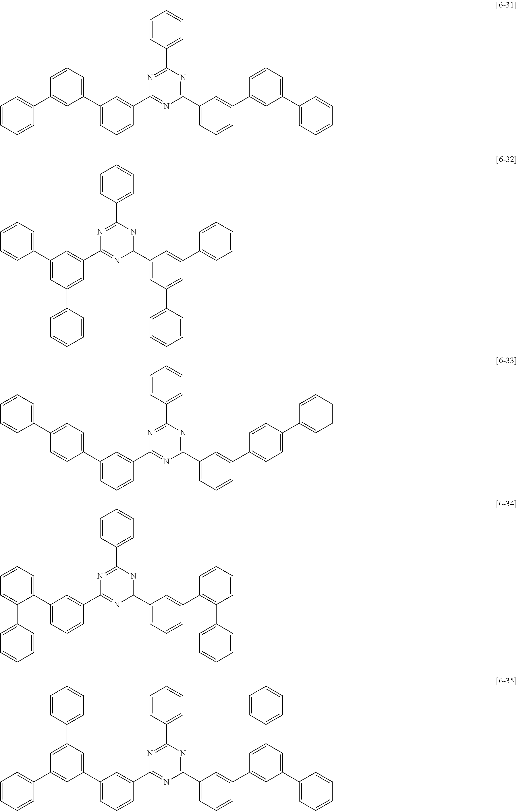


13. The composition for an organic optoelectric device as claimed in claim 7 , wherein the composition further comprises a phosphorescent dopant.
14. An organic optoelectric device comprising
an anode and a cathode facing each other, and
at least one organic layer between the anode and the cathode,
wherein the organic layer includes the compound for an organic optoelectric device as claimed in claim 1 .
15. The organic optoelectric device as claimed in claim 14 , wherein the organic layer comprises an emission layer,
the emission layer comprises the compound for an organic optoelectric device.
16. The organic optoelectric device as claimed in claim 15 , wherein:
the compound for an organic optoelectric device is a host of the emission layer, or
the organic layer further comprises a hole transport auxiliary layer, and the compound for an organic optoelectric device is in the hole transport auxiliary layer.
17. A display device comprising the organic optoelectric device as claimed in claim 14 .
18. An organic optoelectric device comprising
an anode and a cathode facing each other, and
at least one organic layer between the anode and the cathode,
wherein the organic layer includes the composition for an organic optoelectric device as claimed in claim 7 .
19. A display device comprising the organic optoelectric device as claimed in claim 18 .
Applications Claiming Priority (2)
| Application Number | Priority Date | Filing Date | Title |
|---|---|---|---|
| KR1020140150601A KR101829749B1 (en) | 2014-10-31 | 2014-10-31 | Organic compound for optoelectric device and composition for optoelectric device and organic optoelectric device and display device |
| KR10-2014-0150601 | 2014-10-31 |
Publications (2)
| Publication Number | Publication Date |
|---|---|
| US20160126477A1 US20160126477A1 (en) | 2016-05-05 |
| US10193081B2 true US10193081B2 (en) | 2019-01-29 |
Family
ID=55129378
Family Applications (1)
| Application Number | Title | Priority Date | Filing Date |
|---|---|---|---|
| US14/864,288 Active 2037-02-24 US10193081B2 (en) | 2014-10-31 | 2015-09-24 | Organic compound for optoelectric device and composition for optoelectric device and organic optoelectric device and display device |
Country Status (6)
| Country | Link |
|---|---|
| US (1) | US10193081B2 (en) |
| EP (1) | EP3015527B1 (en) |
| JP (1) | JP6696753B2 (en) |
| KR (1) | KR101829749B1 (en) |
| CN (1) | CN105566200B (en) |
| TW (1) | TWI657077B (en) |
Cited By (2)
| Publication number | Priority date | Publication date | Assignee | Title |
|---|---|---|---|---|
| US11177441B2 (en) * | 2014-01-24 | 2021-11-16 | Samsung Sdi Co., Ltd. | Organic compound, composition, organic optoelectronic device, and display device |
| US11542252B2 (en) | 2018-12-28 | 2023-01-03 | Samsung Electronics Co., Ltd. | Heterocyclic compound, composition including the same, and organic light-emitting device including the heterocyclic compound |
Families Citing this family (13)
| Publication number | Priority date | Publication date | Assignee | Title |
|---|---|---|---|---|
| KR101887213B1 (en) * | 2014-08-12 | 2018-08-09 | 삼성에스디아이 주식회사 | Compound, organic optoelectric device and display device |
| US10784447B2 (en) | 2015-04-24 | 2020-09-22 | Samsung Sdi Co., Ltd. | Organic compound, composition, and organic optoelectronic diode |
| WO2017043645A1 (en) * | 2015-09-10 | 2017-03-16 | 東ソー株式会社 | Cyclic azine compound, and production method, production intermediate, and use thereof |
| CN105924383B (en) * | 2016-05-24 | 2018-12-11 | 中节能万润股份有限公司 | Electroluminescent organic material and preparation method thereof and organic electroluminescence device |
| KR101944851B1 (en) * | 2016-09-29 | 2019-02-01 | 엘지디스플레이 주식회사 | Organic compound and organic light emitting diode and organic light emittid display device having the compound |
| KR102037816B1 (en) * | 2016-11-16 | 2019-10-29 | 삼성에스디아이 주식회사 | Organic optoelectronic device and display device |
| CN109790120A (en) * | 2016-11-23 | 2019-05-21 | 广州华睿光电材料有限公司 | The organic mixture of nitrogen-containing hetero carbazole derivates and its application |
| US20190319197A1 (en) * | 2016-11-23 | 2019-10-17 | Guangzhou Chinaray Optoelectronic Materials Ltd. | Organic compound, applications thereof, organic mixture, and organic electronic device |
| KR102109545B1 (en) * | 2016-12-22 | 2020-05-12 | 삼성에스디아이 주식회사 | Composition for organic optoelectric device and organic optoelectric device and display device |
| JP2020061390A (en) * | 2016-12-26 | 2020-04-16 | 出光興産株式会社 | Composition, material for organic electroluminescent element, composition film, organic electroluminescent element, and electronic equipment |
| JP2020061389A (en) * | 2016-12-26 | 2020-04-16 | 出光興産株式会社 | Organic electroluminescence device and electronic device |
| KR102214895B1 (en) * | 2017-12-26 | 2021-02-09 | 삼성에스디아이 주식회사 | Resist underlayer composition, and method of forming patterns using the composition |
| CN112851586B (en) * | 2019-11-27 | 2023-04-18 | 昱镭光电科技股份有限公司 | Electronic active material with phenyl pyrimidine compound as framework, exciplex, organic electroluminescent device and application |
Citations (18)
| Publication number | Priority date | Publication date | Assignee | Title |
|---|---|---|---|---|
| US20040124766A1 (en) * | 2002-10-24 | 2004-07-01 | Satoshi Nakagawa | Organic electroluminescent device |
| US20070190355A1 (en) * | 2004-03-08 | 2007-08-16 | Idemitsu Kosan Co., Ltd | Material for organic electroluminescence device and organic electroluminescence device utilizing the same |
| US20110042654A1 (en) | 2007-09-14 | 2011-02-24 | Sung-Hyun Jung | Organic compound, and organic photoelectric device comprising the same |
| JP2011082238A (en) | 2009-10-05 | 2011-04-21 | Konica Minolta Holdings Inc | Organic electroluminescent element, illuminating device and display device |
| US20110288295A1 (en) * | 2008-12-01 | 2011-11-24 | Sagami Chemical Research Institute | 1,3,5-triazine derivative, process for producing same, and organic electroluminescent device comprising same |
| US20120056171A1 (en) * | 2009-05-15 | 2012-03-08 | Hyung-Sun Kim | Compound for organic photoelectric device and organic photoelectric device including the same |
| WO2012133652A1 (en) * | 2011-03-31 | 2012-10-04 | 富士フイルム株式会社 | Charge transport material, organic electroluminescent element, and illumination device, display device, or light-emitting device characterized by using said element |
| WO2012161382A1 (en) * | 2011-05-26 | 2012-11-29 | Cheil Industries Inc. | Compound for organic optoelectronic device, organic light emitting diode including the same and display including the organic light emitting diode |
| KR101211091B1 (en) | 2009-09-16 | 2012-12-12 | 주식회사 진웅산업 | Light-emitting compound and organic light-emitting device using the same |
| KR101227126B1 (en) | 2011-10-24 | 2013-01-28 | 주식회사 진웅산업 | Light-emitting compound and organic light-emitting device using the same |
| TW201332995A (en) | 2011-11-22 | 2013-08-16 | Idemitsu Kosan Co | Aromatic heterocyclic derivative, material for organic electroluminescent element, and organic electroluminescent element |
| CN103261172A (en) | 2010-12-21 | 2013-08-21 | E.I.内穆尔杜邦公司 | Electronic device including a pyrimidine compound |
| US20130256645A1 (en) | 2010-12-02 | 2013-10-03 | Soo-Hyun Min | Compound for organic optoelectronic device, organic light emitting diode including the same, and display device including the organic light emitting diode |
| KR20140000259A (en) | 2011-02-07 | 2014-01-02 | 이데미쓰 고산 가부시키가이샤 | Biscarbazole derivative and organic electroluminescent element using same |
| WO2014030872A2 (en) | 2012-08-21 | 2014-02-27 | 제일모직 주식회사 | Organic photoelectric element and display device comprising same |
| KR20140057687A (en) | 2011-12-30 | 2014-05-13 | 제일모직주식회사 | Compound for organic optoelectronic device, organic light emitting diode including the same and display including the organic light emitting diode |
| KR101433822B1 (en) | 2013-06-17 | 2014-08-27 | 삼성디스플레이 주식회사 | Organic light emitting diode device |
| KR20150042650A (en) | 2013-10-11 | 2015-04-21 | 제일모직주식회사 | Organic alloy for organic optoelectric device and organic optoelectric device and display device |
-
2014
- 2014-10-31 KR KR1020140150601A patent/KR101829749B1/en active IP Right Grant
-
2015
- 2015-09-24 US US14/864,288 patent/US10193081B2/en active Active
- 2015-10-07 TW TW104132908A patent/TWI657077B/en active
- 2015-10-16 CN CN201510671555.3A patent/CN105566200B/en active Active
- 2015-10-26 EP EP15191522.0A patent/EP3015527B1/en active Active
- 2015-10-30 JP JP2015214710A patent/JP6696753B2/en active Active
Patent Citations (22)
| Publication number | Priority date | Publication date | Assignee | Title |
|---|---|---|---|---|
| US20040124766A1 (en) * | 2002-10-24 | 2004-07-01 | Satoshi Nakagawa | Organic electroluminescent device |
| US20070190355A1 (en) * | 2004-03-08 | 2007-08-16 | Idemitsu Kosan Co., Ltd | Material for organic electroluminescence device and organic electroluminescence device utilizing the same |
| US20110042654A1 (en) | 2007-09-14 | 2011-02-24 | Sung-Hyun Jung | Organic compound, and organic photoelectric device comprising the same |
| US20110288295A1 (en) * | 2008-12-01 | 2011-11-24 | Sagami Chemical Research Institute | 1,3,5-triazine derivative, process for producing same, and organic electroluminescent device comprising same |
| US20120056171A1 (en) * | 2009-05-15 | 2012-03-08 | Hyung-Sun Kim | Compound for organic photoelectric device and organic photoelectric device including the same |
| EP2431445A2 (en) | 2009-05-15 | 2012-03-21 | Cheil Industries Inc. | Compound for organic photoelectric device and organic photoelectric device comprising same |
| CN102421868A (en) | 2009-05-15 | 2012-04-18 | 第一毛织株式会社 | Compound for organic photoelectric device and organic photoelectric device comprising same |
| KR101211091B1 (en) | 2009-09-16 | 2012-12-12 | 주식회사 진웅산업 | Light-emitting compound and organic light-emitting device using the same |
| JP2011082238A (en) | 2009-10-05 | 2011-04-21 | Konica Minolta Holdings Inc | Organic electroluminescent element, illuminating device and display device |
| US20130256645A1 (en) | 2010-12-02 | 2013-10-03 | Soo-Hyun Min | Compound for organic optoelectronic device, organic light emitting diode including the same, and display device including the organic light emitting diode |
| CN103261172A (en) | 2010-12-21 | 2013-08-21 | E.I.内穆尔杜邦公司 | Electronic device including a pyrimidine compound |
| KR20140000259A (en) | 2011-02-07 | 2014-01-02 | 이데미쓰 고산 가부시키가이샤 | Biscarbazole derivative and organic electroluminescent element using same |
| JP2012216819A (en) * | 2011-03-31 | 2012-11-08 | Fujifilm Corp | Charge transport material, organic electroluminescent element, and light-emitting device, display unit or luminaire using that element |
| WO2012133652A1 (en) * | 2011-03-31 | 2012-10-04 | 富士フイルム株式会社 | Charge transport material, organic electroluminescent element, and illumination device, display device, or light-emitting device characterized by using said element |
| WO2012161382A1 (en) * | 2011-05-26 | 2012-11-29 | Cheil Industries Inc. | Compound for organic optoelectronic device, organic light emitting diode including the same and display including the organic light emitting diode |
| US20140027750A1 (en) * | 2011-05-26 | 2014-01-30 | Eun-Sun Yu | Compound for organic optoelectronic device, organic light emitting diode including the same and display including the organic light emitting diode |
| KR101227126B1 (en) | 2011-10-24 | 2013-01-28 | 주식회사 진웅산업 | Light-emitting compound and organic light-emitting device using the same |
| TW201332995A (en) | 2011-11-22 | 2013-08-16 | Idemitsu Kosan Co | Aromatic heterocyclic derivative, material for organic electroluminescent element, and organic electroluminescent element |
| KR20140057687A (en) | 2011-12-30 | 2014-05-13 | 제일모직주식회사 | Compound for organic optoelectronic device, organic light emitting diode including the same and display including the organic light emitting diode |
| WO2014030872A2 (en) | 2012-08-21 | 2014-02-27 | 제일모직 주식회사 | Organic photoelectric element and display device comprising same |
| KR101433822B1 (en) | 2013-06-17 | 2014-08-27 | 삼성디스플레이 주식회사 | Organic light emitting diode device |
| KR20150042650A (en) | 2013-10-11 | 2015-04-21 | 제일모직주식회사 | Organic alloy for organic optoelectric device and organic optoelectric device and display device |
Non-Patent Citations (8)
| Title |
|---|
| Chinese Office Action dated Aug. 9, 2017, of the corresponding Chinese Patent Application No. 201510671555.3. |
| Extended European Search Report dated Mar. 3, 2016 in Corresponding European Patent Application No. 15191522.0. |
| Machine translation for JP 2012-216819 A (publication date-Nov. 2012). * |
| Machine translation for JP 2012-216819 A (publication date—Nov. 2012). * |
| Machine translation for WO 2012/133652 A (publication date-Oct. 2012). * |
| Machine translation for WO 2012/133652 A (publication date—Oct. 2012). * |
| Shin, et al., A new N-fluorenyl carbazole host material: Synthesis, physical properties and applications for highly efficient phosphorescent organic light emitting diodes, Organic Electronics 12 (2011) 785-793. |
| Taiwanese Search Report dated May 25, 2016 in Corresponding Taiwanese Patent Application No. 104132908. |
Cited By (2)
| Publication number | Priority date | Publication date | Assignee | Title |
|---|---|---|---|---|
| US11177441B2 (en) * | 2014-01-24 | 2021-11-16 | Samsung Sdi Co., Ltd. | Organic compound, composition, organic optoelectronic device, and display device |
| US11542252B2 (en) | 2018-12-28 | 2023-01-03 | Samsung Electronics Co., Ltd. | Heterocyclic compound, composition including the same, and organic light-emitting device including the heterocyclic compound |
Also Published As
| Publication number | Publication date |
|---|---|
| KR101829749B1 (en) | 2018-02-19 |
| JP2016088936A (en) | 2016-05-23 |
| TW201615623A (en) | 2016-05-01 |
| EP3015527B1 (en) | 2018-04-11 |
| KR20160051142A (en) | 2016-05-11 |
| CN105566200B (en) | 2019-03-12 |
| US20160126477A1 (en) | 2016-05-05 |
| TWI657077B (en) | 2019-04-21 |
| JP6696753B2 (en) | 2020-05-20 |
| EP3015527A1 (en) | 2016-05-04 |
| CN105566200A (en) | 2016-05-11 |
Similar Documents
| Publication | Publication Date | Title |
|---|---|---|
| US20230209997A1 (en) | Organic alloy for organic optoelectronic device, organic optoelectronic device, and display device | |
| US10193081B2 (en) | Organic compound for optoelectric device and composition for optoelectric device and organic optoelectric device and display device | |
| US20230329097A1 (en) | Composition for organic optoelectronic device, organic optoelectronic device, and display device | |
| US10050212B2 (en) | Organic optoelectric device and display device | |
| US9653690B2 (en) | Organic compound, organic optoelectronic device and display device | |
| US10873033B2 (en) | Organic compound, composition, organic optoelectronic diode, and display device | |
| US20170098778A1 (en) | Composition for organic optoelectric device, organic optoelectric device and display device | |
| US10074810B2 (en) | Organic optoelectric device and display device | |
| US11696498B2 (en) | Compound for an organic optoelectronic device, organic optoelectronic device, and display device using the same | |
| US20160163995A1 (en) | Organic optoelectric device and display device | |
| US11450813B2 (en) | Organic optoelectronic diode and display device | |
| US10312454B2 (en) | Compound for organic optoelectric device, organic optoelectric device and display device | |
| US20170104163A1 (en) | Composition for organic optoelectric diode, organic optoelectric diode, and display device | |
| US10644245B2 (en) | Composition for organic photoelectronic element, organic photoelectronic element, and display apparatus | |
| US10944059B2 (en) | Compound for organic optoelectronic device, organic optoelectronic device, and display device | |
| US11450806B2 (en) | Composition for organic optoelectronic element, organic optoelectronic element, and display device | |
| US20160126472A1 (en) | Composition for organic optoelectronic device, organic optoelectronic device, and display device | |
| US11706975B2 (en) | Compound for organic optoelectronic device, composition for organic optoelectronic device, organic optoelectronic device and display apparatus | |
| US20190198775A1 (en) | Composition and organic optoelectronic device and display device | |
| US20170084845A1 (en) | Organic optoelectronic device and display device | |
| US11678572B2 (en) | Compound for organic optoelectronic device, composition for organic optoelectronic device, organic optoelectronic device and display apparatus | |
| US20180301635A1 (en) | Composition for organic optoelectronic element, organic optoelectronic element, and display device | |
| US20170092873A1 (en) | Composition for organic optoelectronic device, organic optoelectronic device and display device | |
| US11459316B2 (en) | Compound for organic optoelectronic device, composition for organic optoelectronic device, organic optoelectronic device, and display device | |
| US20200111967A1 (en) | Composition for organic optoelectronic device and organic optoelectronic device and display device |
Legal Events
| Date | Code | Title | Description |
|---|---|---|---|
| AS | Assignment |
Owner name: SAMSUNG SDI CO., LTD., KOREA, REPUBLIC OF Free format text: ASSIGNMENT OF ASSIGNORS INTEREST;ASSIGNORS:KIM, HYUNG-SUN;KIM, YOUNG-KWON;RYU, DONG-WAN;AND OTHERS;REEL/FRAME:036649/0797 Effective date: 20150916 |
|
| STCF | Information on status: patent grant |
Free format text: PATENTED CASE |
|
| MAFP | Maintenance fee payment |
Free format text: PAYMENT OF MAINTENANCE FEE, 4TH YEAR, LARGE ENTITY (ORIGINAL EVENT CODE: M1551); ENTITY STATUS OF PATENT OWNER: LARGE ENTITY Year of fee payment: 4 |