US10189230B2 - Method for forming copper film - Google Patents
Method for forming copper film Download PDFInfo
- Publication number
- US10189230B2 US10189230B2 US15/638,099 US201715638099A US10189230B2 US 10189230 B2 US10189230 B2 US 10189230B2 US 201715638099 A US201715638099 A US 201715638099A US 10189230 B2 US10189230 B2 US 10189230B2
- Authority
- US
- United States
- Prior art keywords
- film
- copper
- copper film
- target
- processing module
- Prior art date
- Legal status (The legal status is an assumption and is not a legal conclusion. Google has not performed a legal analysis and makes no representation as to the accuracy of the status listed.)
- Active
Links
Images


Classifications
-
- B—PERFORMING OPERATIONS; TRANSPORTING
- B32—LAYERED PRODUCTS
- B32B—LAYERED PRODUCTS, i.e. PRODUCTS BUILT-UP OF STRATA OF FLAT OR NON-FLAT, e.g. CELLULAR OR HONEYCOMB, FORM
- B32B15/00—Layered products comprising a layer of metal
- B32B15/20—Layered products comprising a layer of metal comprising aluminium or copper
-
- H—ELECTRICITY
- H10—SEMICONDUCTOR DEVICES; ELECTRIC SOLID-STATE DEVICES NOT OTHERWISE PROVIDED FOR
- H10W—GENERIC PACKAGES, INTERCONNECTIONS, CONNECTORS OR OTHER CONSTRUCTIONAL DETAILS OF DEVICES COVERED BY CLASS H10
- H10W20/00—Interconnections in chips, wafers or substrates
- H10W20/01—Manufacture or treatment
- H10W20/071—Manufacture or treatment of dielectric parts thereof
- H10W20/074—Manufacture or treatment of dielectric parts thereof of dielectric parts comprising thin functional dielectric layers, e.g. dielectric etch-stop, barrier, capping or liner layers
- H10W20/077—Manufacture or treatment of dielectric parts thereof of dielectric parts comprising thin functional dielectric layers, e.g. dielectric etch-stop, barrier, capping or liner layers on sidewalls or on top surfaces of conductors
-
- H01L21/768—
-
- H01L23/53238—
-
- H—ELECTRICITY
- H10—SEMICONDUCTOR DEVICES; ELECTRIC SOLID-STATE DEVICES NOT OTHERWISE PROVIDED FOR
- H10P—GENERIC PROCESSES OR APPARATUS FOR THE MANUFACTURE OR TREATMENT OF DEVICES COVERED BY CLASS H10
- H10P14/00—Formation of materials, e.g. in the shape of layers or pillars
- H10P14/40—Formation of materials, e.g. in the shape of layers or pillars of conductive or resistive materials
- H10P14/42—Formation of materials, e.g. in the shape of layers or pillars of conductive or resistive materials using a gas or vapour
- H10P14/44—Physical vapour deposition [PVD]
-
- H—ELECTRICITY
- H10—SEMICONDUCTOR DEVICES; ELECTRIC SOLID-STATE DEVICES NOT OTHERWISE PROVIDED FOR
- H10P—GENERIC PROCESSES OR APPARATUS FOR THE MANUFACTURE OR TREATMENT OF DEVICES COVERED BY CLASS H10
- H10P95/00—Generic processes or apparatus for manufacture or treatments not covered by the other groups of this subclass
- H10P95/90—Thermal treatments, e.g. annealing or sintering
-
- H—ELECTRICITY
- H10—SEMICONDUCTOR DEVICES; ELECTRIC SOLID-STATE DEVICES NOT OTHERWISE PROVIDED FOR
- H10W—GENERIC PACKAGES, INTERCONNECTIONS, CONNECTORS OR OTHER CONSTRUCTIONAL DETAILS OF DEVICES COVERED BY CLASS H10
- H10W20/00—Interconnections in chips, wafers or substrates
- H10W20/01—Manufacture or treatment
- H10W20/031—Manufacture or treatment of conductive parts of the interconnections
- H10W20/032—Manufacture or treatment of conductive parts of the interconnections of conductive barrier, adhesion or liner layers
- H10W20/033—Manufacture or treatment of conductive parts of the interconnections of conductive barrier, adhesion or liner layers in openings in dielectrics
-
- H—ELECTRICITY
- H10—SEMICONDUCTOR DEVICES; ELECTRIC SOLID-STATE DEVICES NOT OTHERWISE PROVIDED FOR
- H10W—GENERIC PACKAGES, INTERCONNECTIONS, CONNECTORS OR OTHER CONSTRUCTIONAL DETAILS OF DEVICES COVERED BY CLASS H10
- H10W20/00—Interconnections in chips, wafers or substrates
- H10W20/01—Manufacture or treatment
- H10W20/031—Manufacture or treatment of conductive parts of the interconnections
- H10W20/032—Manufacture or treatment of conductive parts of the interconnections of conductive barrier, adhesion or liner layers
- H10W20/038—Manufacture or treatment of conductive parts of the interconnections of conductive barrier, adhesion or liner layers covering conductive structures
-
- H—ELECTRICITY
- H10—SEMICONDUCTOR DEVICES; ELECTRIC SOLID-STATE DEVICES NOT OTHERWISE PROVIDED FOR
- H10W—GENERIC PACKAGES, INTERCONNECTIONS, CONNECTORS OR OTHER CONSTRUCTIONAL DETAILS OF DEVICES COVERED BY CLASS H10
- H10W20/00—Interconnections in chips, wafers or substrates
- H10W20/01—Manufacture or treatment
- H10W20/031—Manufacture or treatment of conductive parts of the interconnections
- H10W20/056—Manufacture or treatment of conductive parts of the interconnections by filling conductive material into holes, grooves or trenches
-
- H—ELECTRICITY
- H10—SEMICONDUCTOR DEVICES; ELECTRIC SOLID-STATE DEVICES NOT OTHERWISE PROVIDED FOR
- H10W—GENERIC PACKAGES, INTERCONNECTIONS, CONNECTORS OR OTHER CONSTRUCTIONAL DETAILS OF DEVICES COVERED BY CLASS H10
- H10W20/00—Interconnections in chips, wafers or substrates
- H10W20/40—Interconnections external to wafers or substrates, e.g. back-end-of-line [BEOL] metallisations or vias connecting to gate electrodes
- H10W20/41—Interconnections external to wafers or substrates, e.g. back-end-of-line [BEOL] metallisations or vias connecting to gate electrodes characterised by their conductive parts
- H10W20/425—Barrier, adhesion or liner layers
-
- C—CHEMISTRY; METALLURGY
- C01—INORGANIC CHEMISTRY
- C01G—COMPOUNDS CONTAINING METALS NOT COVERED BY SUBCLASSES C01D OR C01F
- C01G23/00—Compounds of titanium
-
- C—CHEMISTRY; METALLURGY
- C01—INORGANIC CHEMISTRY
- C01G—COMPOUNDS CONTAINING METALS NOT COVERED BY SUBCLASSES C01D OR C01F
- C01G41/00—Compounds of tungsten
Definitions
- the disclosure relates to a method for forming a copper film.
- a damascene method is known as one of the wiring process techniques.
- a barrier film is formed on a surface of an insulating film where a recess is formed.
- the barrier film is generally made of tantalum, tantalum nitride, cobalt or ruthenium.
- a copper film is formed on the barrier film.
- the copper film is formed by, e.g., a sputtering method.
- Japanese Patent Application Publication No. H11-343570 there is disclosed a method for forming a copper film by sputtering, wherein a temperature of a target object having an insulating film is set to a low level of 20° C. or less.
- a temperature of a target object having an insulating film is set to a low level of 20° C. or less.
- a wiring made of copper requires low resistance. However, when a crystal in the copper film has a small particle size, the resistance of the wiring made of copper is increased. Therefore, it is required to form a copper film having low resistance.
- the disclosure provides a method for forming a copper film having low resistance.
- a method for forming a copper film is provided.
- a base film that is a titanium nitride film, a tungsten film or a tungsten nitride film is formed along a surface of an insulating film of an object and a copper film is formed on the base film of the object cooled to a temperature of 209 K or less.
- the object having a general barrier film made of tantalum, tantalum nitride, cobalt or ruthenium is cooled to a low temperature and the copper film is formed on the barrier film. Even if the temperature of the copper film is increased, the particle size of the crystal in the copper film is not increased.
- the object having the base film that is a titanium nitride film, a tungsten film or a tungsten nitride film is cooled to a low temperature and the copper film is formed on the base film.
- the temperature increase operation for increasing the particle size of the crystal in the copper film may be performed by placing the object having the copper film under a normal temperature (e.g., room temperature) environment.
- a film thickness of the base film may be set such that the base film becomes in an amorphous state.
- the film thickness of the base film may be set to be greater than or equal to 1.0 nm and smaller than or equal to 2.5 nm.
- recess may be formed in the insulating film and the base film may be formed along a surface of the insulating film defining the recess.
- the base film and the copper film may be formed on a relatively flat surface of the insulating film.
- the wiring may be formed by applying plasma etching to the copper film.
- FIG. 1 is a flowchart showing a method for forming a copper film according to an embodiment
- FIG. 2 is an enlarged cross sectional view showing an example of an object to which the method shown in FIG. 1 can be applied;
- FIG. 3 shows a processing system that can be used for implementing the method shown in FIG. 1 ;
- FIG. 4A schematically shows an example of a processing module used for executing a step ST 2 of the method shown in FIG. 1 and FIG. 4B is an enlarged cross sectional view showing an object after the execution of the step ST 2 ;
- FIG. 5A schematically shows an example of a processing module used for executing a step ST 3 of the method shown in FIG. 1 and FIG. 5B is an enlarged cross sectional view showing an object after the execution of the step ST 3 ;
- FIG. 6 schematically shows an example of a processing module used for executing a step ST 4 of the method shown in FIG. 1 ;
- FIG. 7A schematically shows an example of a processing module used for executing a step ST 5 of the method shown in FIG. 1 and FIG. 7B is an enlarged cross sectional view showing an object after the execution of the step ST 5 ;
- FIG. 8 is a graph showing an evaluation result of dependence of a sheet resistance of a copper on a film thickness of a base film
- FIG. 9 is a graph showing an evaluation result of dependence of a sheet resistance of the copper film on a cooling temperature in the step ST 4 ;
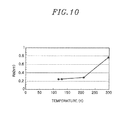
- FIG. 10 is a graph showing an evaluation result of dependence of surface roughness of the copper film on the cooling temperature in the step ST 4 .
- FIG. 1 is a flowchart showing a method for forming a copper film according to an embodiment.
- a method MT shown in FIG. 1 is a method for forming a copper film on a surface of an insulating film of an object.
- the method MT includes steps ST 1 to ST 6 .
- the steps ST 1 to ST 6 will be described in detail later.
- FIG. 2 is an enlarged cross sectional view showing an example of an object to which the method shown in FIG. 1 can be applied.
- An object W 1 shown in FIG. 2 has a disc shape, for example.
- the object W 1 has a base layer 10 and an insulating film 12 .
- the insulating film 12 is formed on the base layer 10 .
- the insulating film 12 is made of, e.g., silicon oxide.
- the insulating film 12 may be made of a low dielectric material (Low-K material).
- a recess 12 r is formed on the insulating film 12 .
- the recess 12 r extends from a top surface 12 t of the insulating film 12 along a film thickness direction of the insulating film 12 .
- the recess 12 r may be, e.g., a groove or a hole.
- the recess 12 r is formed by, e.g., photolithography and etching.
- FIG. 3 shows a processing system that can be used for implementing the method shown in FIG. 1 .
- a processing system 100 shown in FIG. 3 includes a loader module 102 , load-lock modules 104 and 106 , a transfer module 108 , a plurality of processing modules 110 a to 110 h and a control unit 112 .
- the number of the processing modules of the processing system 100 is eight in the example shown in FIG. 3 but not limited thereto.
- the loader module 102 is configured to transfer a target object under an atmospheric pressure environment.
- a plurality of tables 114 is attached to the loader module 102 .
- a container 116 capable of accommodating a plurality of target objects is mounted on each of the tables 114 .
- the container 116 may be, e.g., a FOUP (Front-Opening Unified Pod).
- the loader module 102 provides a chamber 102 c .
- a transfer unit 102 t is provided in the chamber 102 c .
- the transfer unit 102 t may include a robot arm for transferring the target object while holding the target object.
- the loader module 102 is connected to the load-lock modules 104 and 106 .
- the transfer unit 102 t transfers the target object between the container 116 and the load-lock module 104 or between the container 116 and the load-lock module 106 .
- the load-lock modules 104 and 106 provide chambers 104 c and 106 c for preliminary evacuation, respectively.
- the transfer module 108 is connected to the load-lock modules 104 and 106 .
- the transfer module 108 provides an evacuable transfer chamber 108 c .
- a transfer unit 108 t is provided in the transfer chamber 108 c .
- the transfer unit 108 t may include a robot arm for transferring a target object while holding the target object.
- the transfer module 108 is connected to a plurality of processing modules 110 a to 110 h .
- the transfer unit 108 t of the transfer module 108 transfers the target object between one of the load-lock modules 104 and 106 and one of the processing modules 110 a to 110 h and between any two of the processing modules 110 a to 110 h.
- the processing modules 110 a to 110 h include processing modules for executing a plurality of steps of the method MT.
- the processing module 110 a is a plasma etching apparatus for performing etching in a step ST 1 to be described later.
- the processing module 110 a is, e.g., a capacitively coupled plasma etching apparatus.
- the processing module 110 a may be an inductively coupled plasma etching apparatus or a plasma etching apparatus for exciting a gas by a surface wave such as a microwave.
- the processing module 110 b is a film forming apparatus used for forming a barrier film in a step ST 2 .
- the processing module 110 b is, e.g., a sputtering apparatus.
- the processing module 110 c is a film forming apparatus used for forming a base film in a step ST 3 .
- the processing module 110 c is, e.g., a sputtering apparatus.
- the processing module 110 d is a processing apparatus used for cooling a target object in a step ST 4 .
- the processing module 110 e is a film forming apparatus used for forming a copper film in a step ST 5 .
- the processing module 110 e is, e.g., a sputtering apparatus.
- the film formation in two or more steps among the steps ST 2 , ST 3 and ST 5 may be performed by a film forming apparatus that is a single processing module.
- the steps ST 4 and ST 5 may be performed by the same processing module.
- a control unit 112 is configured to control the loader module 102 , the transfer module 108 and the processing modules 110 a to 110 h .
- the control unit 112 may be a computer having a storage device, e.g., a processor and a memory.
- a storage device e.g., a processor and a memory.
- a program for controlling the respective components of the processing system 100 and a recipe data for implementing the method MT in the processing system 100 are stored.
- the processor operates in accordance with the program and the recipe data stored in the storage device and outputs control signals for controlling the respective components of the processing system 100 to the respective components.
- FIG. 4A schematically shows an example of a processing module used for executing the step ST 2 of the method shown in FIG. 1 .
- FIG. 4B is an enlarged cross sectional view showing a target object after the execution of the step ST 2 .
- FIG. 5A schematically shows an example of a processing module used for executing the step ST 3 of the method shown in FIG. 1 .
- FIG. 5B is an enlarged cross sectional view showing a target object after the execution of the step ST 3 .
- FIG. 6 schematically shows an example of a processing module used for executing the step ST 4 of the method shown in FIG. 1 .
- FIG. 7A schematically shows an example of a processing module used for executing the step ST 5 of the method shown in FIG. 1 .
- FIG. 7B is an enlarged cross sectional view showing a target object after the execution of the step ST 5 .
- the step ST 1 of the method MT is executed.
- the target object W 1 is etched.
- the target object W 1 is mounted on a mounting table provided in a chamber of the processing module 110 a .
- the chamber of the processing module 110 a plasma of a rare gas such as Ar gas or the like is generated.
- a bias high frequency power is supplied to a lower electrode of the mounting table.
- ions generated in the chamber are attracted to the target object W 1 .
- sputter etching is performed on the target object W 1 , thereby slightly etching a surface of the target object W 1 .
- a target object W 2 is obtained from the target object W 1 .
- the step ST 2 of the method MT is executed.
- a barrier film is formed on a surface of the target object W 2 .
- the surface on which the barrier film is formed includes a surface of the insulating film 12 which defines the recess 12 r .
- the barrier film is made of tantalum, tantalum nitride, cobalt or ruthenium.
- the target object W 2 is transferred from the processing module 110 a to the processing module 110 b through the transfer module 108 .
- the barrier film formation in the step ST 2 is performed.
- the processing module 110 b is a sputtering apparatus.
- the processing module 110 b includes a chamber main body 120 b , a stage 122 b , a target holder 126 b , a power supply 130 b , a gas supply unit 132 b and a gas exhaust unit 134 b .
- the chamber main body 120 b provides an inner space as a chamber Sb.
- the stage 122 b is provided in the chamber Sb.
- the stage 122 b is configured to hold a target object mounted thereon.
- the stage 122 b may include an electrostatic chuck.
- the stage 122 b is supported by a rotational shaft 124 b . By rotating the rotational shaft 124 b by a driving unit, the stage 122 b can rotate about a central axis thereof.
- a target holder 126 b is provided above the stage 122 b .
- the target holder 126 b holds the target 128 b .
- the target 128 b is made of a material forming the barrier film.
- the target holder 126 b is connected to the power supply 130 b .
- the power supply 130 b may be a DC power supply or a high frequency power supply.
- a gas is supplied from a gas supply unit 132 b into the chamber Sb.
- the gas supplied from the gas supply unit 132 b is a rare gas such as Ar gas or the like, or an inert gas.
- the gas exhaust unit 134 b is connected to the chamber main body 120 b .
- the gas exhaust unit 134 b is a device for evacuating the chamber Sb and may include a pressure control valve and a vacuum pump such as a turbo molecular pump or the like.
- the object W 2 mounted on the stage 122 b is held on the stage 122 b and the stage 122 b is rotated.
- the gas is supplied from the gas supply unit 132 b into the chamber Sb.
- the chamber Sb is evacuated by the gas exhaust unit 134 b .
- a voltage is applied from the power supply 130 b to the target holder 126 b . Accordingly, plasma is generated around the target 128 b and ions in the plasma are attracted to the target 128 b .
- ions collide with the target 128 b a material forming the target 128 b is sputtered from the target 128 b .
- the sputtered material is deposited on the object W 2 .
- the barrier film 14 is formed on a surface of the object W 2 .
- an object W 3 is obtained.
- the target object W 3 includes a base layer 10 , an insulating film 12 and a barrier film 14 .
- the barrier film 14 is made of tantalum, tantalum nitride, cobalt or ruthenium.
- the step ST 3 of the method MT is executed.
- a base film is formed on a surface of the barrier film 14 of the object W 3 .
- the base film is formed along the surface of the insulating film 12 of the object W 3 .
- the base film is a titanium nitride film, a tungsten film or a tungsten nitride film.
- the object W 3 is transferred from the processing module 110 b to the processing module 110 c through the transfer module 108 .
- the base film formation in the step ST 3 is performed.
- the processing module 110 c is the same sputtering apparatus as that constituting the processing module 110 b .
- the processing module 110 c includes a chamber main body 120 c , a stage 122 c , a target holder 126 c , a power supply 130 c , a gas supply unit 132 c and a gas exhaust unit 134 c .
- the chamber main body 120 c provides a chamber Sc.
- the stage 122 c is provided in the chamber Sc.
- the stage 122 c is supported by a rotational shaft 124 c .
- the stage 122 c rotates about a central axis thereof by the rotation of the rotation 124 c by a driving unit.
- the target holder 126 c holds the target 128 c above the stage 122 c .
- the target 128 c is made of a material forming the base film.
- the configurations of the power supply 130 c , the gas supply unit 132 c and the gas exhaust unit 134 c are the same as those of the power supply 130 b , the gas supply unit 132 b and the gas exhaust unit 134 b , respectively.
- the object W 3 mounted on the stage 122 c is held on the stage 122 c and the stage 122 c is rotated.
- a gas (rare gas such as Ar gas or the like or another inert gas) is supplied from the gas supply unit 132 c into the chamber Sc.
- the chamber Sc is evacuated by the gas exhaust unit 134 c .
- a voltage is applied from the power supply 130 c to the target holder 126 c . Accordingly, plasma is generated around the target 128 c and ions in the plasma are attracted to the target 128 c .
- the ions collide with the target 128 c a material forming the target 128 c is sputtered from the target 128 c .
- the object W 4 includes a base layer 10 , an insulating film 12 , a barrier film 14 and a base film 16 .
- the base film 16 is a titanium nitride film, a tungsten film or a tungsten nitride film.
- a film thickness of the base film 16 is set such that the base film 16 becomes in an amorphous state.
- the base film 16 is formed to have a film thickness of greater than or equal to 1.0 nm and smaller than or equal to 2.5 nm.
- the step ST 4 of the method MT is executed.
- the object W 4 is cooled to a temperature of 209 K or less.
- the object W 4 is transferred from the processing module 110 c to the processing module 110 d through the transfer module 108 .
- the cooling of the object in the step ST 4 is performed.
- the processing module 110 d includes a chamber main body 120 d , a stage 122 d and a chiller 140 d .
- the chamber main body 120 d provides an inner space as a chamber Sd.
- the stage 122 d is provided in the chamber Sd.
- An object is mounted on the stage 122 d .
- the chiller 140 d is coupled to the stage 122 d .
- the chiller 140 d is configured to cool the target object mounted on the stage 122 d to a temperature of 209 K or less.
- the chiller 140 d may be a freezer using, e.g., a Gifford-McMahon cycle (G.M. cycle).
- the object W 4 mounted on the stage 122 d is cooled to a temperature of 209 K or less by the chiller 140 d.
- the step ST 5 of the method MT is executed.
- a copper film is formed on the base film 16 of the object W 4 cooled in the step ST 4 .
- the object W 4 is transferred from the processing module 110 d to the processing module 110 e through the transfer module 108 .
- the copper film formation in the step ST 5 is performed.
- the processing module 110 e is the same sputtering apparatus as that constituting the processing module 110 b .
- the processing module 110 e includes a chamber main body 120 e , a stage 122 e , a target holder 126 e , a power supply 130 e , a gas supply unit 132 e and a gas exhaust unit 134 e .
- the chamber main body 120 e provides a chamber Se.
- the stage 122 e is provided in the chamber Se.
- the stage 122 e is supported by a rotational shaft 124 e and rotates about a central axis thereof by the rotation of the rotational shaft 124 e by a driving unit.
- the target holder 126 e holds the target 128 e above the stage 122 e .
- the target 128 e is made of copper.
- the configurations of the power supply 130 e , the gas supply unit 132 e and the gas exhaust unit 134 e are the same as those of the power supply 130 b , the gas supply unit 132 b and the gas exhaust unit 134 b.
- the object W 4 cooled in the step ST 4 is mounted on the stage 122 e and held on the stage 122 e .
- the stage 122 e is rotated.
- a gas (rare gas such as Ar gas or the like or another inert gas) is supplied from the gas supply unit 132 e into the chamber Se.
- the chamber Se is evacuated by the gas exhaust unit 134 e .
- a voltage is applied from the power supply 130 e to the target holder 126 e . Accordingly, plasma is generated around the target 128 e and ions in the plasma are attracted to the target 128 e .
- the object W 5 includes a base layer 10 , an insulating film 14 , a base film 16 and a copper film 18 .
- the step ST 6 of the method MT is executed.
- the object W 5 having a low temperature after the execution of the step ST 5 is subjected to a temperature increase operation.
- the temperature of the object W 5 may be increased by a heating unit.
- the temperature of the object W 5 is naturally increased.
- the temperature of the object W 5 is increased under a normal temperature (e.g., room temperature) environment without using a heating unit.
- the temperature of the object W 5 is increased in the load-lock module 104 or 106 .
- the object having a general barrier film made of tantalum, tantalum nitride, cobalt or ruthenium is cooled to a low temperature and a copper film is formed on the barrier film. Even if the temperature of the copper film is increased, a particle size of a crystal in the copper film is not increased.
- the object W 4 having the base film 16 that is a titanium nitride film, a tungsten film or a tungsten nitride film is cooled to a low temperature (209 K or less) in the step ST 4 and the copper film 18 is formed on the base film 16 .
- the copper film 18 formed in the step ST 5 has a relatively small crystal particle before the temperature increase operation in the step ST 6 .
- the particle size of the crystal in the copper film 18 is increased.
- the crystal in the copper film was oriented dominantly in the ( 111 ) orientation.
- the crystal in the copper film 18 was oriented in other orientations such as the ( 200 ) orientation, in addition to the ( 111 ) orientation. Therefore, in the method MT, the copper film 18 having a crystal having a large particle size is obtained. Accordingly, in the method MT, the copper film 18 having low resistance is formed.
- the step ST 2 of forming the barrier film 14 may be omitted.
- the base film 16 may be formed directly on the insulating film 12 .
- the insulating film 12 on which the recess is formed has been described an example of the object to which the method MT is applied.
- the copper film 18 is formed to form copper wiring in the recess has been described.
- the base film 16 and the copper film 18 may be formed on the insulating film having a relatively flat surface. In that case, the copper wiring may be formed by etching the copper film 18 later.
- test that has been executed to examine the method MT will be described.
- the present disclosure is not limited by the test to be described below.
- FIG. 8 is a graph showing an evaluation result of the dependence of the sheet resistance of the copper film on the film thickness of the base film.
- the horizontal axis represents the film thickness of the base film 16
- the vertical axis represents the sheet resistance of the copper film.
- the sheet resistance of the copper film 18 which is obtained by the method MT was considerably low. Especially when the film thickness of the base film 16 was greater than or equal to 1.0 nm and smaller than or equal to 2.5 nm, the sheet resistance of the copper film 18 was even lower.
- a plurality of samples was obtained by cooling an object having a silicon oxide film (step ST 4 ), forming a copper film (film thickness: 50 nm) on the silicon oxide film of the cooled object (step ST 5 ), and increasing a temperature of the object having the copper film under a normal temperature environment (step ST 6 ).
- the samples were obtained by setting the temperature of the object to different levels in the step ST 4 .
- a particle size of a crystal of the copper film formed on the cooled silicon oxide film is increased when the temperature of the copper film on the silicon oxide film is increased, as in the case of the copper film formed on the cooled base film 16 .
- sheet resistances and arithmetic mean roughnesses Ra of the copper films of the samples were measured.
- FIG. 9 is a graph showing an evaluation result of the dependence of the sheet resistance of the copper film on the cooling temperature in the step ST 4 .
- the horizontal axis represents the cooling temperature of the object in the step ST 4
- the vertical axis represents the sheet resistance.
- FIG. 10 is a graph showing an evaluation result of the dependence of the surface roughness of the copper film on the cooling temperature in the ST 4 .
- the horizontal axis represents the cooling temperature of the object in the step ST 4
- the vertical axis represents the arithmetic mean roughness Ra.
- the sheet resistance of the copper film after the temperature increase operation in the step ST 6 was decreased by cooling the object to a temperature of 209 K or less in the step ST 4 .
- the surface roughness of the copper film after the temperature increase operation in the step ST 6 was decreased by cooling the object to a temperature of 209 K or less in the step ST 4 .
- the particle size of the crystal in the copper film of each sample is about 500 nm, which is considerably larger than a particle size (about 50 nm) of a crystal in a general copper film.
Landscapes
- Internal Circuitry In Semiconductor Integrated Circuit Devices (AREA)
- Physical Vapour Deposition (AREA)
- Electrodes Of Semiconductors (AREA)
Abstract
A method for forming a copper film is provided. In the method, a base film that is a titanium nitride film, a tungsten film or a tungsten nitride film is formed along a surface of an insulating film of an object. A copper film is formed on the base film of the object cooled to a temperature of 209 K or less.
Description
This application claims priority to Japanese Patent Application No. 2016-128799 filed on Jun. 29, 2016, the entire contents of which are incorporated herein by reference.
The disclosure relates to a method for forming a copper film.
In a semiconductor device manufacturing process, wiring processing is performed. A damascene method is known as one of the wiring process techniques. In the damascene method, a barrier film is formed on a surface of an insulating film where a recess is formed. The barrier film is generally made of tantalum, tantalum nitride, cobalt or ruthenium. Then, a copper film is formed on the barrier film. The copper film is formed by, e.g., a sputtering method.
In Japanese Patent Application Publication No. H11-343570, there is disclosed a method for forming a copper film by sputtering, wherein a temperature of a target object having an insulating film is set to a low level of 20° C. or less. In the method disclosed in Japanese Patent Application Publication No. H11-343570, by performing the sputtering of copper in a state where the temperature of the target object is set to a low level, agglomeration of copper is suppressed and a copper film has a flat surface.
A wiring made of copper requires low resistance. However, when a crystal in the copper film has a small particle size, the resistance of the wiring made of copper is increased. Therefore, it is required to form a copper film having low resistance.
In view of the above, the disclosure provides a method for forming a copper film having low resistance.
In accordance with one aspect, there is provided a method for forming a copper film is provided. In the method, a base film that is a titanium nitride film, a tungsten film or a tungsten nitride film is formed along a surface of an insulating film of an object and a copper film is formed on the base film of the object cooled to a temperature of 209 K or less.
The object having a general barrier film made of tantalum, tantalum nitride, cobalt or ruthenium is cooled to a low temperature and the copper film is formed on the barrier film. Even if the temperature of the copper film is increased, the particle size of the crystal in the copper film is not increased. In the method according to one aspect, the object having the base film that is a titanium nitride film, a tungsten film or a tungsten nitride film is cooled to a low temperature and the copper film is formed on the base film. When the temperature of the copper film formed on the base film is increased, the particle size of the crystal in the copper film is increased. Therefore, in accordance with the method according to one aspect, the copper film having low resistance is formed. In one embodiment, the temperature increase operation for increasing the particle size of the crystal in the copper film may be performed by placing the object having the copper film under a normal temperature (e.g., room temperature) environment.
A film thickness of the base film may be set such that the base film becomes in an amorphous state. The film thickness of the base film may be set to be greater than or equal to 1.0 nm and smaller than or equal to 2.5 nm.
In one embodiment, recess may be formed in the insulating film and the base film may be formed along a surface of the insulating film defining the recess. In another embodiment, the base film and the copper film may be formed on a relatively flat surface of the insulating film. The wiring may be formed by applying plasma etching to the copper film.
As described above, it is possible to form the copper film having low resistance.
The objects and features of the disclosure will become apparent from the following description of embodiments, given in conjunction with the accompanying drawings, in which:
Hereinafter, various embodiments will be described in detail with reference to the accompanying drawings. Like reference numerals will be used for like or corresponding parts throughout the respective drawings.
A recess 12 r is formed on the insulating film 12. The recess 12 r extends from a top surface 12 t of the insulating film 12 along a film thickness direction of the insulating film 12. The recess 12 r may be, e.g., a groove or a hole. The recess 12 r is formed by, e.g., photolithography and etching.
Hereinafter, a processing system that can be used for implementing the method MT will be described prior to detailed description of the method MT. FIG. 3 shows a processing system that can be used for implementing the method shown in FIG. 1 . A processing system 100 shown in FIG. 3 includes a loader module 102, load- lock modules 104 and 106, a transfer module 108, a plurality of processing modules 110 a to 110 h and a control unit 112. The number of the processing modules of the processing system 100 is eight in the example shown in FIG. 3 but not limited thereto.
The loader module 102 is configured to transfer a target object under an atmospheric pressure environment. A plurality of tables 114 is attached to the loader module 102. A container 116 capable of accommodating a plurality of target objects is mounted on each of the tables 114. The container 116 may be, e.g., a FOUP (Front-Opening Unified Pod).
The loader module 102 provides a chamber 102 c. A transfer unit 102 t is provided in the chamber 102 c. The transfer unit 102 t may include a robot arm for transferring the target objet while holding the target object. The loader module 102 is connected to the load- lock modules 104 and 106. The transfer unit 102 t transfers the target object between the container 116 and the load-lock module 104 or between the container 116 and the load-lock module 106.
The load- lock modules 104 and 106 provide chambers 104 c and 106 c for preliminary evacuation, respectively. The transfer module 108 is connected to the load- lock modules 104 and 106. The transfer module 108 provides an evacuable transfer chamber 108 c. A transfer unit 108 t is provided in the transfer chamber 108 c. The transfer unit 108 t may include a robot arm for transferring a target object while holding the target object. The transfer module 108 is connected to a plurality of processing modules 110 a to 110 h. The transfer unit 108 t of the transfer module 108 transfers the target object between one of the load- lock modules 104 and 106 and one of the processing modules 110 a to 110 h and between any two of the processing modules 110 a to 110 h.
The processing modules 110 a to 110 h include processing modules for executing a plurality of steps of the method MT. In one example, the processing module 110 a is a plasma etching apparatus for performing etching in a step ST1 to be described later. The processing module 110 a is, e.g., a capacitively coupled plasma etching apparatus. Further, the processing module 110 a may be an inductively coupled plasma etching apparatus or a plasma etching apparatus for exciting a gas by a surface wave such as a microwave.
In one example, the processing module 110 b is a film forming apparatus used for forming a barrier film in a step ST2. The processing module 110 b is, e.g., a sputtering apparatus. In one example, the processing module 110 c is a film forming apparatus used for forming a base film in a step ST3. The processing module 110 c is, e.g., a sputtering apparatus. In one example, the processing module 110 d is a processing apparatus used for cooling a target object in a step ST4. In one example, the processing module 110 e is a film forming apparatus used for forming a copper film in a step ST5. The processing module 110 e is, e.g., a sputtering apparatus. The film formation in two or more steps among the steps ST2, ST3 and ST5 may be performed by a film forming apparatus that is a single processing module. The steps ST4 and ST5 may be performed by the same processing module.
A control unit 112 is configured to control the loader module 102, the transfer module 108 and the processing modules 110 a to 110 h. The control unit 112 may be a computer having a storage device, e.g., a processor and a memory. In the storage device, a program for controlling the respective components of the processing system 100 and a recipe data for implementing the method MT in the processing system 100 are stored. The processor operates in accordance with the program and the recipe data stored in the storage device and outputs control signals for controlling the respective components of the processing system 100 to the respective components.
Referring back to FIG. 1 , the method MT will be described in detail. Hereinafter, the method MT will be described based on the case of using the processing system 100 as an example. However, the method MT may be performed by using another processing system different from the processing system 100. In the following description, FIGS. 1, 4A and 4B, 5A and 5B, 6, 7A and 7B will be referred to. FIG. 4A schematically shows an example of a processing module used for executing the step ST2 of the method shown in FIG. 1 . FIG. 4B is an enlarged cross sectional view showing a target object after the execution of the step ST2. FIG. 5A schematically shows an example of a processing module used for executing the step ST3 of the method shown in FIG. 1 . FIG. 5B is an enlarged cross sectional view showing a target object after the execution of the step ST3. FIG. 6 schematically shows an example of a processing module used for executing the step ST4 of the method shown in FIG. 1 . FIG. 7A schematically shows an example of a processing module used for executing the step ST5 of the method shown in FIG. 1 . FIG. 7B is an enlarged cross sectional view showing a target object after the execution of the step ST5.
As shown in FIG. 1 , first, the step ST1 of the method MT is executed. In the step ST1, the target object W1 is etched. In the step ST1 of one embodiment, the target object W1 is mounted on a mounting table provided in a chamber of the processing module 110 a. In the chamber of the processing module 110 a, plasma of a rare gas such as Ar gas or the like is generated. A bias high frequency power is supplied to a lower electrode of the mounting table. In the step ST1, ions generated in the chamber are attracted to the target object W1. In the step ST1, sputter etching is performed on the target object W1, thereby slightly etching a surface of the target object W1. As a result of the step ST1, a target object W2 is obtained from the target object W1.
Next, the step ST2 of the method MT is executed. In the step ST2, a barrier film is formed on a surface of the target object W2. The surface on which the barrier film is formed includes a surface of the insulating film 12 which defines the recess 12 r. The barrier film is made of tantalum, tantalum nitride, cobalt or ruthenium. In one embodiment, after the execution of the step ST1, the target object W2 is transferred from the processing module 110 a to the processing module 110 b through the transfer module 108. In the processing module 110 b, the barrier film formation in the step ST2 is performed.
As shown in FIG. 4A , the processing module 110 b is a sputtering apparatus. The processing module 110 b includes a chamber main body 120 b, a stage 122 b, a target holder 126 b, a power supply 130 b, a gas supply unit 132 b and a gas exhaust unit 134 b. The chamber main body 120 b provides an inner space as a chamber Sb. The stage 122 b is provided in the chamber Sb. The stage 122 b is configured to hold a target object mounted thereon. For example, the stage 122 b may include an electrostatic chuck. The stage 122 b is supported by a rotational shaft 124 b. By rotating the rotational shaft 124 b by a driving unit, the stage 122 b can rotate about a central axis thereof.
A target holder 126 b is provided above the stage 122 b. The target holder 126 b holds the target 128 b. The target 128 b is made of a material forming the barrier film. The target holder 126 b is connected to the power supply 130 b. The power supply 130 b may be a DC power supply or a high frequency power supply.
In the processing module 110 b, a gas is supplied from a gas supply unit 132 b into the chamber Sb. The gas supplied from the gas supply unit 132 b is a rare gas such as Ar gas or the like, or an inert gas. Further, in the processing module 110 b, the gas exhaust unit 134 b is connected to the chamber main body 120 b. The gas exhaust unit 134 b is a device for evacuating the chamber Sb and may include a pressure control valve and a vacuum pump such as a turbo molecular pump or the like.
In the step ST2 of an embodiment, the object W2 mounted on the stage 122 b is held on the stage 122 b and the stage 122 b is rotated. The gas is supplied from the gas supply unit 132 b into the chamber Sb. The chamber Sb is evacuated by the gas exhaust unit 134 b. A voltage is applied from the power supply 130 b to the target holder 126 b. Accordingly, plasma is generated around the target 128 b and ions in the plasma are attracted to the target 128 b. When ions collide with the target 128 b, a material forming the target 128 b is sputtered from the target 128 b. The sputtered material is deposited on the object W2. Accordingly, the barrier film 14 is formed on a surface of the object W2. As a consequence, an object W3 is obtained. As shown in FIG. 4B , the target object W3 includes a base layer 10, an insulating film 12 and a barrier film 14. The barrier film 14 is made of tantalum, tantalum nitride, cobalt or ruthenium.
Next, the step ST3 of the method MT is executed. In the step ST3, a base film is formed on a surface of the barrier film 14 of the object W3. In other words, the base film is formed along the surface of the insulating film 12 of the object W3. The base film is a titanium nitride film, a tungsten film or a tungsten nitride film. In one embodiment, after the execution of the step ST2, the object W3 is transferred from the processing module 110 b to the processing module 110 c through the transfer module 108. In the processing module 110 c, the base film formation in the step ST3 is performed.
As shown in FIG. 5A , the processing module 110 c is the same sputtering apparatus as that constituting the processing module 110 b. The processing module 110 c includes a chamber main body 120 c, a stage 122 c, a target holder 126 c, a power supply 130 c, a gas supply unit 132 c and a gas exhaust unit 134 c. The chamber main body 120 c provides a chamber Sc. The stage 122 c is provided in the chamber Sc. The stage 122 c is supported by a rotational shaft 124 c. The stage 122 c rotates about a central axis thereof by the rotation of the rotation 124 c by a driving unit. The target holder 126 c holds the target 128 c above the stage 122 c. The target 128 c is made of a material forming the base film. The configurations of the power supply 130 c, the gas supply unit 132 c and the gas exhaust unit 134 c are the same as those of the power supply 130 b, the gas supply unit 132 b and the gas exhaust unit 134 b, respectively.
In the step ST3 of one embodiment, the object W3 mounted on the stage 122 c is held on the stage 122 c and the stage 122 c is rotated. A gas (rare gas such as Ar gas or the like or another inert gas) is supplied from the gas supply unit 132 c into the chamber Sc. The chamber Sc is evacuated by the gas exhaust unit 134 c. A voltage is applied from the power supply 130 c to the target holder 126 c. Accordingly, plasma is generated around the target 128 c and ions in the plasma are attracted to the target 128 c. When the ions collide with the target 128 c, a material forming the target 128 c is sputtered from the target 128 c. The sputtered material is deposited on the object W3. As a consequence, a base film 16 is formed on a surface of the object W3, and an object W4 is obtained. As shown in FIG. 5B , the object W4 includes a base layer 10, an insulating film 12, a barrier film 14 and a base film 16. The base film 16 is a titanium nitride film, a tungsten film or a tungsten nitride film.
In one embodiment, a film thickness of the base film 16 is set such that the base film 16 becomes in an amorphous state. For example, in the step ST3, the base film 16 is formed to have a film thickness of greater than or equal to 1.0 nm and smaller than or equal to 2.5 nm.
Next, the step ST4 of the method MT is executed. In the step ST4, the object W4 is cooled to a temperature of 209 K or less. In one embodiment, after the execution of the step ST3, the object W4 is transferred from the processing module 110 c to the processing module 110 d through the transfer module 108. In the processing module 110 d, the cooling of the object in the step ST4 is performed.
As shown in FIG. 6 , the processing module 110 d includes a chamber main body 120 d, a stage 122 d and a chiller 140 d. The chamber main body 120 d provides an inner space as a chamber Sd. The stage 122 d is provided in the chamber Sd. An object is mounted on the stage 122 d. The chiller 140 d is coupled to the stage 122 d. The chiller 140 d is configured to cool the target object mounted on the stage 122 d to a temperature of 209 K or less. The chiller 140 d may be a freezer using, e.g., a Gifford-McMahon cycle (G.M. cycle). In the step ST4 of one embodiment, the object W4 mounted on the stage 122 d is cooled to a temperature of 209 K or less by the chiller 140 d.
Next, the step ST5 of the method MT is executed. In the step ST5, a copper film is formed on the base film 16 of the object W4 cooled in the step ST4. In one embodiment, after the execution of the step ST4, the object W4 is transferred from the processing module 110 d to the processing module 110 e through the transfer module 108. In the processing module 110 e, the copper film formation in the step ST5 is performed.
As shown in FIG. 7A , the processing module 110 e is the same sputtering apparatus as that constituting the processing module 110 b. The processing module 110 e includes a chamber main body 120 e, a stage 122 e, a target holder 126 e, a power supply 130 e, a gas supply unit 132 e and a gas exhaust unit 134 e. The chamber main body 120 e provides a chamber Se. The stage 122 e is provided in the chamber Se. The stage 122 e is supported by a rotational shaft 124 e and rotates about a central axis thereof by the rotation of the rotational shaft 124 e by a driving unit. The target holder 126 e holds the target 128 e above the stage 122 e. The target 128 e is made of copper. The configurations of the power supply 130 e, the gas supply unit 132 e and the gas exhaust unit 134 e are the same as those of the power supply 130 b, the gas supply unit 132 b and the gas exhaust unit 134 b.
In the step ST5 of one embodiment, the object W4 cooled in the step ST4 is mounted on the stage 122 e and held on the stage 122 e. The stage 122 e is rotated. A gas (rare gas such as Ar gas or the like or another inert gas) is supplied from the gas supply unit 132 e into the chamber Se. The chamber Se is evacuated by the gas exhaust unit 134 e. A voltage is applied from the power supply 130 e to the target holder 126 e. Accordingly, plasma is generated around the target 128 e and ions in the plasma are attracted to the target 128 e. When the ions collide with the target 128 e, a material, i.e., copper, forming the target 128 e is sputtered from the target 128 e. The sputtered material is deposited on the object W4. Accordingly, a copper film 18 is formed on the base film 16 of the object W4, and an object W5 is obtained. As shown in FIG. 7B , the object W5 includes a base layer 10, an insulating film 14, a base film 16 and a copper film 18.
Next, the step ST6 of the method MT is executed. In the step ST6, the object W5 having a low temperature after the execution of the step ST5 is subjected to a temperature increase operation. The temperature of the object W5 may be increased by a heating unit. However, in one embodiment, the temperature of the object W5 is naturally increased. In other words, in the step ST6 of one embodiment, the temperature of the object W5 is increased under a normal temperature (e.g., room temperature) environment without using a heating unit. For example, the temperature of the object W5 is increased in the load- lock module 104 or 106.
The object having a general barrier film made of tantalum, tantalum nitride, cobalt or ruthenium is cooled to a low temperature and a copper film is formed on the barrier film. Even if the temperature of the copper film is increased, a particle size of a crystal in the copper film is not increased. In the method MT, the object W4 having the base film 16 that is a titanium nitride film, a tungsten film or a tungsten nitride film is cooled to a low temperature (209 K or less) in the step ST4 and the copper film 18 is formed on the base film 16. Although copper particles are agglomerated by surface diffusion on the object set to a relatively high temperature, the agglomeration of copper is suppressed on the base film 16 of the object W4 cooled to a low temperature. As a result, the copper film 18 formed in the step ST5 has a relatively small crystal particle before the temperature increase operation in the step ST6.
When the temperature of the copper film 18 formed on the base film 16 is increased, the particle size of the crystal in the copper film 18 is increased. According to a test performed by the present inventors, when a copper film was formed directly on the barrier film 14, the crystal in the copper film was oriented dominantly in the (111) orientation. On the other hand, when the temperature of the copper film 18 formed on the base film 16 was increased, the crystal in the copper film 18 was oriented in other orientations such as the (200) orientation, in addition to the (111) orientation. Therefore, in the method MT, the copper film 18 having a crystal having a large particle size is obtained. Accordingly, in the method MT, the copper film 18 having low resistance is formed.
While the embodiments have been described, various modifications may be made without being limited to the above-described embodiments. For example, the step ST2 of forming the barrier film 14 may be omitted. In other words, the base film 16 may be formed directly on the insulating film 12.
An object having the insulating film 12 on which the recess is formed has been described an example of the object to which the method MT is applied. In other words, an example in which the copper film 18 is formed to form copper wiring in the recess has been described. However, in the method MT, the base film 16 and the copper film 18 may be formed on the insulating film having a relatively flat surface. In that case, the copper wiring may be formed by etching the copper film 18 later.
Hereinafter, a test that has been executed to examine the method MT will be described. The present disclosure is not limited by the test to be described below.
(Evaluation of Dependence of Sheet Resistance of Copper Film on Film Thickness of Base Film)
In the test, a plurality of samples was obtained by forming the copper film 18 on base films 16 having different film thicknesses by performing the method MT. The film thickness of the copper film 18 was 50 nm. In the step ST4, the object was cooled to 100 K. In the step ST6, the temperature of the object after the formation of the copper film was increased under a normal temperature environment. Then, the sheet resistance of the copper film of each sample was measured. The result thereof is shown in FIG. 8 . FIG. 8 is a graph showing an evaluation result of the dependence of the sheet resistance of the copper film on the film thickness of the base film. In FIG. 8 , the horizontal axis represents the film thickness of the base film 16, and the vertical axis represents the sheet resistance of the copper film. As can be seen from FIG. 8 , the sheet resistance of the copper film 18 which is obtained by the method MT was considerably low. Especially when the film thickness of the base film 16 was greater than or equal to 1.0 nm and smaller than or equal to 2.5 nm, the sheet resistance of the copper film 18 was even lower.
(Dependence of Surface Roughness and Sheet Resistance of Copper Film on Cooling Temperature in Step ST4)
In a test, a plurality of samples was obtained by cooling an object having a silicon oxide film (step ST4), forming a copper film (film thickness: 50 nm) on the silicon oxide film of the cooled object (step ST5), and increasing a temperature of the object having the copper film under a normal temperature environment (step ST6). The samples were obtained by setting the temperature of the object to different levels in the step ST4. A particle size of a crystal of the copper film formed on the cooled silicon oxide film is increased when the temperature of the copper film on the silicon oxide film is increased, as in the case of the copper film formed on the cooled base film 16. In the test, sheet resistances and arithmetic mean roughnesses Ra of the copper films of the samples were measured. FIG. 9 is a graph showing an evaluation result of the dependence of the sheet resistance of the copper film on the cooling temperature in the step ST4. In FIG. 9 , the horizontal axis represents the cooling temperature of the object in the step ST4, and the vertical axis represents the sheet resistance. FIG. 10 is a graph showing an evaluation result of the dependence of the surface roughness of the copper film on the cooling temperature in the ST4. In FIG. 10 , the horizontal axis represents the cooling temperature of the object in the step ST4, and the vertical axis represents the arithmetic mean roughness Ra. As can be seen from FIG. 9 , the sheet resistance of the copper film after the temperature increase operation in the step ST6 was decreased by cooling the object to a temperature of 209 K or less in the step ST4. As can be seen from FIG. 10 , the surface roughness of the copper film after the temperature increase operation in the step ST6 was decreased by cooling the object to a temperature of 209 K or less in the step ST4. The particle size of the crystal in the copper film of each sample is about 500 nm, which is considerably larger than a particle size (about 50 nm) of a crystal in a general copper film.
While the disclosure has been shown and described with respect to the embodiments, it will be understood by those skilled in the art that various changes and modifications may be made without departing from the scope of the disclosure as defined in the following claims.
Claims (5)
1. A method for forming a copper film, the method comprising:
forming a base film along a surface of an insulating film of an object, the base film being one of a titanium nitride film, a tungsten film or a tungsten nitride film; and
forming a copper film on the base film of the object having the insulating film and the base film after cooling the object to a temperature of 209 K or less.
2. The method of claim 1 , wherein a film thickness of the base film is set such that the base film becomes in an amorphous state.
3. The method of claim 2 , wherein the film thickness of the base film is set to be greater than or equal to 1.0 nm and smaller than or equal to 2.5 nm.
4. The method of claim 1 , further comprising: increasing a temperature of the object including the insulating film, the base film and the copper film.
5. The method of claim 1 , wherein a recess is formed on the insulating film and the base film is formed along a surface of the insulating film which defines the recess.
Applications Claiming Priority (2)
| Application Number | Priority Date | Filing Date | Title |
|---|---|---|---|
| JP2016128799A JP6788393B2 (en) | 2016-06-29 | 2016-06-29 | How to form a copper film |
| JP2016-128799 | 2016-06-29 |
Publications (2)
| Publication Number | Publication Date |
|---|---|
| US20180001597A1 US20180001597A1 (en) | 2018-01-04 |
| US10189230B2 true US10189230B2 (en) | 2019-01-29 |
Family
ID=60806038
Family Applications (1)
| Application Number | Title | Priority Date | Filing Date |
|---|---|---|---|
| US15/638,099 Active US10189230B2 (en) | 2016-06-29 | 2017-06-29 | Method for forming copper film |
Country Status (3)
| Country | Link |
|---|---|
| US (1) | US10189230B2 (en) |
| JP (1) | JP6788393B2 (en) |
| KR (1) | KR101965957B1 (en) |
Cited By (1)
| Publication number | Priority date | Publication date | Assignee | Title |
|---|---|---|---|---|
| US12463022B2 (en) | 2022-10-11 | 2025-11-04 | Tokyo Electron Limited | Placing table and substrate processing apparatus |
Citations (4)
| Publication number | Priority date | Publication date | Assignee | Title |
|---|---|---|---|---|
| KR960016833B1 (en) | 1993-11-11 | 1996-12-21 | Hyundai Electronics Ind | Forming method of metal film for anti-diffusion |
| JPH11343570A (en) | 1998-04-28 | 1999-12-14 | Internatl Business Mach Corp <Ibm> | Material depositing method for material depositing device |
| KR100576363B1 (en) | 2003-05-30 | 2006-05-03 | 삼성전자주식회사 | In Situ Chemical Vapor Deposition Metal Process and Chemical Vapor Deposition Equipment Used Thereof |
| US9728414B2 (en) * | 2006-12-19 | 2017-08-08 | Cypress Semiconductor Corporation | Method of depositing copper using physical vapor deposition |
Family Cites Families (7)
| Publication number | Priority date | Publication date | Assignee | Title |
|---|---|---|---|---|
| JP3672941B2 (en) * | 1993-03-24 | 2005-07-20 | 川崎マイクロエレクトロニクス株式会社 | Wiring structure for semiconductor integrated circuit |
| JP2000183064A (en) * | 1998-12-16 | 2000-06-30 | Matsushita Electronics Industry Corp | Semiconductor device and manufacturing method thereof |
| US6541371B1 (en) * | 1999-02-08 | 2003-04-01 | Novellus Systems, Inc. | Apparatus and method for depositing superior Ta(N)/copper thin films for barrier and seed applications in semiconductor processing |
| US6398929B1 (en) * | 1999-10-08 | 2002-06-04 | Applied Materials, Inc. | Plasma reactor and shields generating self-ionized plasma for sputtering |
| JP4746234B2 (en) * | 1999-10-15 | 2011-08-10 | エーエスエム インターナショナル エヌ.ヴェー. | Method for depositing nanolaminate thin films on sensitive surfaces |
| JP4169950B2 (en) * | 2001-05-18 | 2008-10-22 | Necエレクトロニクス株式会社 | Manufacturing method of semiconductor device |
| US8492897B2 (en) * | 2011-09-14 | 2013-07-23 | International Business Machines Corporation | Microstructure modification in copper interconnect structures |
-
2016
- 2016-06-29 JP JP2016128799A patent/JP6788393B2/en active Active
-
2017
- 2017-06-27 KR KR1020170081202A patent/KR101965957B1/en active Active
- 2017-06-29 US US15/638,099 patent/US10189230B2/en active Active
Patent Citations (5)
| Publication number | Priority date | Publication date | Assignee | Title |
|---|---|---|---|---|
| KR960016833B1 (en) | 1993-11-11 | 1996-12-21 | Hyundai Electronics Ind | Forming method of metal film for anti-diffusion |
| JPH11343570A (en) | 1998-04-28 | 1999-12-14 | Internatl Business Mach Corp <Ibm> | Material depositing method for material depositing device |
| US6210541B1 (en) | 1998-04-28 | 2001-04-03 | International Business Machines Corporation | Process and apparatus for cold copper deposition to enhance copper plating fill |
| KR100576363B1 (en) | 2003-05-30 | 2006-05-03 | 삼성전자주식회사 | In Situ Chemical Vapor Deposition Metal Process and Chemical Vapor Deposition Equipment Used Thereof |
| US9728414B2 (en) * | 2006-12-19 | 2017-08-08 | Cypress Semiconductor Corporation | Method of depositing copper using physical vapor deposition |
Cited By (1)
| Publication number | Priority date | Publication date | Assignee | Title |
|---|---|---|---|---|
| US12463022B2 (en) | 2022-10-11 | 2025-11-04 | Tokyo Electron Limited | Placing table and substrate processing apparatus |
Also Published As
| Publication number | Publication date |
|---|---|
| KR20180002530A (en) | 2018-01-08 |
| JP2018006452A (en) | 2018-01-11 |
| JP6788393B2 (en) | 2020-11-25 |
| US20180001597A1 (en) | 2018-01-04 |
| KR101965957B1 (en) | 2019-04-04 |
Similar Documents
| Publication | Publication Date | Title |
|---|---|---|
| KR20240134812A (en) | Methods for forming structures with desired crystallinity for mram applications | |
| US11542592B2 (en) | Film forming system and method for forming film on substrate | |
| US10563304B2 (en) | Methods and apparatus for dynamically treating atomic layer deposition films in physical vapor deposition chambers | |
| JP2008218659A (en) | Semiconductor device manufacturing method, semiconductor manufacturing apparatus, and program | |
| US20190385908A1 (en) | Treatment And Doping Of Barrier Layers | |
| US20140251945A1 (en) | Method of etching metal layer | |
| TW202100781A (en) | Methods of forming a metal containing material | |
| US11640918B2 (en) | Stage device, power supply mechanism, and processing apparatus | |
| US10189230B2 (en) | Method for forming copper film | |
| JP2010056353A (en) | Manufacturing method of semiconductor device | |
| KR20210113044A (en) | Wafer processing method | |
| JP5719212B2 (en) | Film forming method, resputtering method, and film forming apparatus | |
| TW202348822A (en) | Apparatus and method for fabricating pvd perovskite films | |
| US11832524B2 (en) | Method for processing substrate, processing apparatus, and processing system | |
| TW202422735A (en) | Multi-chamber semiconductor processing system | |
| US10014145B2 (en) | Vacuum exhaust method | |
| US12595552B2 (en) | Module for flipping substrates in vacuum | |
| US20230051865A1 (en) | Pvd apparatus | |
| US20260049393A1 (en) | Physical vapor deposition module and system including same | |
| US12492465B2 (en) | PVD apparatus and method | |
| CN121237683A (en) | Wafer indexing mechanism for processing modules |
Legal Events
| Date | Code | Title | Description |
|---|---|---|---|
| AS | Assignment |
Owner name: TOKYO ELECTRON LIMITED, JAPAN Free format text: ASSIGNMENT OF ASSIGNORS INTEREST;ASSIGNORS:TOSHIMA, HIROYUKI;SHIMADA, ATSUSHI;HIRASAWA, TATSUO;AND OTHERS;SIGNING DATES FROM 20170626 TO 20170712;REEL/FRAME:043026/0309 |
|
| STCF | Information on status: patent grant |
Free format text: PATENTED CASE |
|
| MAFP | Maintenance fee payment |
Free format text: PAYMENT OF MAINTENANCE FEE, 4TH YEAR, LARGE ENTITY (ORIGINAL EVENT CODE: M1551); ENTITY STATUS OF PATENT OWNER: LARGE ENTITY Year of fee payment: 4 |