US10186367B2 - Electronic component and board having the same - Google Patents
Electronic component and board having the same Download PDFInfo
- Publication number
- US10186367B2 US10186367B2 US14/995,084 US201614995084A US10186367B2 US 10186367 B2 US10186367 B2 US 10186367B2 US 201614995084 A US201614995084 A US 201614995084A US 10186367 B2 US10186367 B2 US 10186367B2
- Authority
- US
- United States
- Prior art keywords
- electronic component
- insulating coating
- coating layer
- external electrodes
- board
- Prior art date
- Legal status (The legal status is an assumption and is not a legal conclusion. Google has not performed a legal analysis and makes no representation as to the accuracy of the status listed.)
- Active, expires
Links
- 239000011247 coating layer Substances 0.000 claims abstract description 32
- 239000004020 conductor Substances 0.000 claims abstract description 14
- 239000010410 layer Substances 0.000 claims description 37
- 238000007747 plating Methods 0.000 claims description 26
- 229910052751 metal Inorganic materials 0.000 claims description 19
- 239000002184 metal Substances 0.000 claims description 19
- 239000000463 material Substances 0.000 claims description 4
- 229910000679 solder Inorganic materials 0.000 claims description 2
- PXHVJJICTQNCMI-UHFFFAOYSA-N Nickel Chemical compound [Ni] PXHVJJICTQNCMI-UHFFFAOYSA-N 0.000 description 14
- 239000003990 capacitor Substances 0.000 description 11
- KDLHZDBZIXYQEI-UHFFFAOYSA-N Palladium Chemical compound [Pd] KDLHZDBZIXYQEI-UHFFFAOYSA-N 0.000 description 9
- 239000010949 copper Substances 0.000 description 7
- 229910000859 α-Fe Inorganic materials 0.000 description 7
- 239000000853 adhesive Substances 0.000 description 5
- 230000001070 adhesive effect Effects 0.000 description 5
- 229910052759 nickel Inorganic materials 0.000 description 5
- RYGMFSIKBFXOCR-UHFFFAOYSA-N Copper Chemical compound [Cu] RYGMFSIKBFXOCR-UHFFFAOYSA-N 0.000 description 4
- 229910052802 copper Inorganic materials 0.000 description 4
- 239000010931 gold Substances 0.000 description 4
- 229910045601 alloy Inorganic materials 0.000 description 3
- 239000000956 alloy Substances 0.000 description 3
- 230000003247 decreasing effect Effects 0.000 description 3
- 229910052763 palladium Inorganic materials 0.000 description 3
- BASFCYQUMIYNBI-UHFFFAOYSA-N platinum Chemical compound [Pt] BASFCYQUMIYNBI-UHFFFAOYSA-N 0.000 description 3
- 239000000843 powder Substances 0.000 description 3
- 230000004308 accommodation Effects 0.000 description 2
- 229910002113 barium titanate Inorganic materials 0.000 description 2
- 230000008901 benefit Effects 0.000 description 2
- 239000003989 dielectric material Substances 0.000 description 2
- 230000000694 effects Effects 0.000 description 2
- 239000011521 glass Substances 0.000 description 2
- PCHJSUWPFVWCPO-UHFFFAOYSA-N gold Chemical compound [Au] PCHJSUWPFVWCPO-UHFFFAOYSA-N 0.000 description 2
- 229910052737 gold Inorganic materials 0.000 description 2
- 238000005245 sintering Methods 0.000 description 2
- 239000010936 titanium Substances 0.000 description 2
- 239000004593 Epoxy Substances 0.000 description 1
- 229910018605 Ni—Zn Inorganic materials 0.000 description 1
- BQCADISMDOOEFD-UHFFFAOYSA-N Silver Chemical compound [Ag] BQCADISMDOOEFD-UHFFFAOYSA-N 0.000 description 1
- ATJFFYVFTNAWJD-UHFFFAOYSA-N Tin Chemical compound [Sn] ATJFFYVFTNAWJD-UHFFFAOYSA-N 0.000 description 1
- RTAQQCXQSZGOHL-UHFFFAOYSA-N Titanium Chemical compound [Ti] RTAQQCXQSZGOHL-UHFFFAOYSA-N 0.000 description 1
- 229910007565 Zn—Cu Inorganic materials 0.000 description 1
- 229910052782 aluminium Inorganic materials 0.000 description 1
- XAGFODPZIPBFFR-UHFFFAOYSA-N aluminium Chemical compound [Al] XAGFODPZIPBFFR-UHFFFAOYSA-N 0.000 description 1
- PNEYBMLMFCGWSK-UHFFFAOYSA-N aluminium oxide Inorganic materials [O-2].[O-2].[O-2].[Al+3].[Al+3] PNEYBMLMFCGWSK-UHFFFAOYSA-N 0.000 description 1
- JRPBQTZRNDNNOP-UHFFFAOYSA-N barium titanate Chemical compound [Ba+2].[Ba+2].[O-][Ti]([O-])([O-])[O-] JRPBQTZRNDNNOP-UHFFFAOYSA-N 0.000 description 1
- 239000000919 ceramic Substances 0.000 description 1
- 239000011248 coating agent Substances 0.000 description 1
- 238000000576 coating method Methods 0.000 description 1
- 229910052593 corundum Inorganic materials 0.000 description 1
- 230000007547 defect Effects 0.000 description 1
- 230000007257 malfunction Effects 0.000 description 1
- 230000004048 modification Effects 0.000 description 1
- 238000012986 modification Methods 0.000 description 1
- -1 or the like Substances 0.000 description 1
- 229910052697 platinum Inorganic materials 0.000 description 1
- 229920001296 polysiloxane Polymers 0.000 description 1
- 229910052709 silver Inorganic materials 0.000 description 1
- 239000004332 silver Substances 0.000 description 1
- 238000005476 soldering Methods 0.000 description 1
- VEALVRVVWBQVSL-UHFFFAOYSA-N strontium titanate Chemical compound [Sr+2].[O-][Ti]([O-])=O VEALVRVVWBQVSL-UHFFFAOYSA-N 0.000 description 1
- 239000000758 substrate Substances 0.000 description 1
- 229910052719 titanium Inorganic materials 0.000 description 1
- 229910001845 yogo sapphire Inorganic materials 0.000 description 1
Images


Classifications
-
- H—ELECTRICITY
- H01—ELECTRIC ELEMENTS
- H01F—MAGNETS; INDUCTANCES; TRANSFORMERS; SELECTION OF MATERIALS FOR THEIR MAGNETIC PROPERTIES
- H01F27/00—Details of transformers or inductances, in general
- H01F27/28—Coils; Windings; Conductive connections
- H01F27/29—Terminals; Tapping arrangements for signal inductances
- H01F27/292—Surface mounted devices
-
- H—ELECTRICITY
- H01—ELECTRIC ELEMENTS
- H01F—MAGNETS; INDUCTANCES; TRANSFORMERS; SELECTION OF MATERIALS FOR THEIR MAGNETIC PROPERTIES
- H01F17/00—Fixed inductances of the signal type
- H01F17/0006—Printed inductances
- H01F17/0013—Printed inductances with stacked layers
-
- H—ELECTRICITY
- H01—ELECTRIC ELEMENTS
- H01F—MAGNETS; INDUCTANCES; TRANSFORMERS; SELECTION OF MATERIALS FOR THEIR MAGNETIC PROPERTIES
- H01F17/00—Fixed inductances of the signal type
- H01F17/0006—Printed inductances
- H01F17/0033—Printed inductances with the coil helically wound around a magnetic core
-
- H—ELECTRICITY
- H01—ELECTRIC ELEMENTS
- H01G—CAPACITORS; CAPACITORS, RECTIFIERS, DETECTORS, SWITCHING DEVICES, LIGHT-SENSITIVE OR TEMPERATURE-SENSITIVE DEVICES OF THE ELECTROLYTIC TYPE
- H01G2/00—Details of capacitors not covered by a single one of groups H01G4/00-H01G11/00
- H01G2/02—Mountings
- H01G2/06—Mountings specially adapted for mounting on a printed-circuit support
-
- H—ELECTRICITY
- H01—ELECTRIC ELEMENTS
- H01G—CAPACITORS; CAPACITORS, RECTIFIERS, DETECTORS, SWITCHING DEVICES, LIGHT-SENSITIVE OR TEMPERATURE-SENSITIVE DEVICES OF THE ELECTROLYTIC TYPE
- H01G4/00—Fixed capacitors; Processes of their manufacture
- H01G4/002—Details
- H01G4/005—Electrodes
- H01G4/012—Form of non-self-supporting electrodes
-
- H—ELECTRICITY
- H01—ELECTRIC ELEMENTS
- H01G—CAPACITORS; CAPACITORS, RECTIFIERS, DETECTORS, SWITCHING DEVICES, LIGHT-SENSITIVE OR TEMPERATURE-SENSITIVE DEVICES OF THE ELECTROLYTIC TYPE
- H01G4/00—Fixed capacitors; Processes of their manufacture
- H01G4/002—Details
- H01G4/228—Terminals
- H01G4/232—Terminals electrically connecting two or more layers of a stacked or rolled capacitor
-
- H—ELECTRICITY
- H01—ELECTRIC ELEMENTS
- H01G—CAPACITORS; CAPACITORS, RECTIFIERS, DETECTORS, SWITCHING DEVICES, LIGHT-SENSITIVE OR TEMPERATURE-SENSITIVE DEVICES OF THE ELECTROLYTIC TYPE
- H01G4/00—Fixed capacitors; Processes of their manufacture
- H01G4/30—Stacked capacitors
-
- H—ELECTRICITY
- H01—ELECTRIC ELEMENTS
- H01G—CAPACITORS; CAPACITORS, RECTIFIERS, DETECTORS, SWITCHING DEVICES, LIGHT-SENSITIVE OR TEMPERATURE-SENSITIVE DEVICES OF THE ELECTROLYTIC TYPE
- H01G4/00—Fixed capacitors; Processes of their manufacture
- H01G4/40—Structural combinations of fixed capacitors with other electric elements, the structure mainly consisting of a capacitor, e.g. RC combinations
-
- H—ELECTRICITY
- H05—ELECTRIC TECHNIQUES NOT OTHERWISE PROVIDED FOR
- H05K—PRINTED CIRCUITS; CASINGS OR CONSTRUCTIONAL DETAILS OF ELECTRIC APPARATUS; MANUFACTURE OF ASSEMBLAGES OF ELECTRICAL COMPONENTS
- H05K1/00—Printed circuits
- H05K1/02—Details
- H05K1/11—Printed elements for providing electric connections to or between printed circuits
- H05K1/111—Pads for surface mounting, e.g. lay-out
-
- H—ELECTRICITY
- H05—ELECTRIC TECHNIQUES NOT OTHERWISE PROVIDED FOR
- H05K—PRINTED CIRCUITS; CASINGS OR CONSTRUCTIONAL DETAILS OF ELECTRIC APPARATUS; MANUFACTURE OF ASSEMBLAGES OF ELECTRICAL COMPONENTS
- H05K1/00—Printed circuits
- H05K1/18—Printed circuits structurally associated with non-printed electric components
- H05K1/181—Printed circuits structurally associated with non-printed electric components associated with surface mounted components
-
- H—ELECTRICITY
- H05—ELECTRIC TECHNIQUES NOT OTHERWISE PROVIDED FOR
- H05K—PRINTED CIRCUITS; CASINGS OR CONSTRUCTIONAL DETAILS OF ELECTRIC APPARATUS; MANUFACTURE OF ASSEMBLAGES OF ELECTRICAL COMPONENTS
- H05K9/00—Screening of apparatus or components against electric or magnetic fields
- H05K9/0007—Casings
- H05K9/002—Casings with localised screening
- H05K9/0022—Casings with localised screening of components mounted on printed circuit boards [PCB]
- H05K9/0024—Shield cases mounted on a PCB, e.g. cans or caps or conformal shields
- H05K9/0026—Shield cases mounted on a PCB, e.g. cans or caps or conformal shields integrally formed from metal sheet
-
- H—ELECTRICITY
- H01—ELECTRIC ELEMENTS
- H01F—MAGNETS; INDUCTANCES; TRANSFORMERS; SELECTION OF MATERIALS FOR THEIR MAGNETIC PROPERTIES
- H01F17/00—Fixed inductances of the signal type
- H01F17/0006—Printed inductances
- H01F2017/0066—Printed inductances with a magnetic layer
-
- H—ELECTRICITY
- H01—ELECTRIC ELEMENTS
- H01G—CAPACITORS; CAPACITORS, RECTIFIERS, DETECTORS, SWITCHING DEVICES, LIGHT-SENSITIVE OR TEMPERATURE-SENSITIVE DEVICES OF THE ELECTROLYTIC TYPE
- H01G4/00—Fixed capacitors; Processes of their manufacture
- H01G4/002—Details
- H01G4/018—Dielectrics
- H01G4/06—Solid dielectrics
- H01G4/08—Inorganic dielectrics
- H01G4/12—Ceramic dielectrics
- H01G4/1209—Ceramic dielectrics characterised by the ceramic dielectric material
- H01G4/1218—Ceramic dielectrics characterised by the ceramic dielectric material based on titanium oxides or titanates
- H01G4/1227—Ceramic dielectrics characterised by the ceramic dielectric material based on titanium oxides or titanates based on alkaline earth titanates
-
- H—ELECTRICITY
- H05—ELECTRIC TECHNIQUES NOT OTHERWISE PROVIDED FOR
- H05K—PRINTED CIRCUITS; CASINGS OR CONSTRUCTIONAL DETAILS OF ELECTRIC APPARATUS; MANUFACTURE OF ASSEMBLAGES OF ELECTRICAL COMPONENTS
- H05K2201/00—Indexing scheme relating to printed circuits covered by H05K1/00
- H05K2201/10—Details of components or other objects attached to or integrated in a printed circuit board
- H05K2201/10007—Types of components
- H05K2201/10015—Non-printed capacitor
-
- H—ELECTRICITY
- H05—ELECTRIC TECHNIQUES NOT OTHERWISE PROVIDED FOR
- H05K—PRINTED CIRCUITS; CASINGS OR CONSTRUCTIONAL DETAILS OF ELECTRIC APPARATUS; MANUFACTURE OF ASSEMBLAGES OF ELECTRICAL COMPONENTS
- H05K2201/00—Indexing scheme relating to printed circuits covered by H05K1/00
- H05K2201/10—Details of components or other objects attached to or integrated in a printed circuit board
- H05K2201/10007—Types of components
- H05K2201/1003—Non-printed inductor
Definitions
- the present disclosure relates to an electronic component and a board having the same.
- inductors and capacitors are representative passive elements configuring an electronic circuit to remove noise therefrom.
- Such an inductor is manufactured by forming a magnetic body including a coil therein, and subsequently, forming external electrodes on outer surfaces of the magnetic body.
- the capacitor an electronic component, may be manufactured by forming a capacitor body including a dielectric material and internal electrodes, and then, forming external electrodes on outer surfaces of the capacitor body.
- An aspect of the present disclosure may provide an electronic component in which the occurrence of short circuits is decreased by suppressing plating solution spreading, and a board having the same.
- an electronic component may include a body having a bottom surface provided as a mounting surface and a top surface opposing the bottom surface, first and second external electrodes disposed to be spaced apart from each other on the bottom surface of the body, and insulating coating layers disposed on the top and bottom surfaces of the body, such that plating solution spreading may be suppressed in the electronic component.
- a board having an electronic component may include a printed circuit board on which first and second electrode pads are formed, and the electronic component as described above, mounted on the printed circuit board.
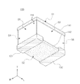
- FIG. 1 is a perspective view schematically illustrating an electronic component according to an exemplary embodiment in the present disclosure
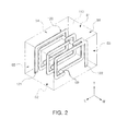
- FIG. 2 is a perspective view schematically illustrating a body according to the exemplary embodiment in the present disclosure
- FIG. 3 is an exploded perspective view of FIG. 2 ;
- FIG. 4 is an exploded perspective view schematically illustrating a body according to another exemplary embodiment in the present disclosure.
- FIG. 5 is a view of surface S 5 of the electronic component according to the present disclosure.
- FIG. 6 is a view of surface S 3 of the electronic component according to the present disclosure.
- FIG. 7 is a perspective view schematically illustrating a board having an electronic component according to another exemplary embodiment in the present disclosure.
- FIG. 8 is a cross-sectional view taken along line A-A′ of FIG. 7 .
- FIG. 1 is a perspective view schematically illustrating an electronic component according to an exemplary embodiment in the present disclosure.
- the electronic component 100 may include a body 110 , external electrodes 131 and 132 , and insulating coating layers 141 and 142 .
- the body 110 may include dielectric layers or magnetic layers, and include a conductor part therein.
- the body 110 is not particularly limited, but may have, for example, a hexahedral shape.
- a ‘length direction’ refers to an ‘L’ direction of FIG. 1
- a ‘width direction’ refers to a ‘W’ direction of FIG.
- a ‘thickness direction’ refers to a ‘T’ direction of FIG. 1 .
- the ‘thickness direction’ may be the same as a direction perpendicular to amounting surface of the electronic component.
- the body 110 may have top and bottom surfaces S 1 and S 2 opposing each other in the thickness direction, first and second side surfaces S 3 and S 4 opposing each other in the width direction, and third and fourth end surfaces S 5 and S 6 opposing each other in the length direction.
- FIG. 2 is a perspective view schematically illustrating the body according to the exemplary embodiment in the present disclosure
- FIG. 3 is an exploded perspective view of FIG. 2 .
- the body 110 may be an inductor body including a coil 120 having a coil shape formed therein, as illustrated in FIG. 2 .
- a conductor part disposed in the body may be the coil 120 .
- the inductor body 110 is formed by stacking a plurality of magnetic layers 111 , wherein the plurality of magnetic layers 111 forming the inductor body 110 may be in a sintered state, and adjacent magnetic layers may be integrated so that boundaries therebetween are not readily apparent without the use of a scanning electron microscope (SEM).
- SEM scanning electron microscope
- the inductor body 110 may contain an Al 2 O 3 -based dielectric material or ferrite known in the art such as Mn—Zn-based ferrite, Ni—Zn-based ferrite, Ni—Zn—Cu-based ferrite, Mn—Mg-based ferrite, Ba-based ferrite, Li-based ferrite, or the like.
- the coil 120 may be formed by an electrical connection of a coil pattern 125 formed by printing a conductive paste containing a conductive metal on the plurality of magnetic layers 111 forming the inductor body 110 to a predetermined thickness.
- Vias 123 may be formed in predetermined positions in respective magnetic layers 111 on which the coil pattern 125 is printed, and the coil patterns 125 formed on the respective magnetic layers 111 may be connected to each other by the vias 123 to thereby form a single coil 120 .
- the conductive metal forming the coil pattern 125 is not particularly limited as long as it has sufficient electrical conductivity.
- silver (Ag), palladium (Pd), aluminum (Al), nickel (Ni), titanium (Ti), gold (Au), copper (Cu), platinum (Pt), or the like, or alloys thereof, may be used as the conductive metal.
- the coil 120 may be formed in a direction perpendicular to a substrate mounting surface of the inductor body 110 .
- First and second lead portions 121 and 122 of the coil 120 may be exposed to the same surface of the inductor body 110 as each other.
- the first and second lead portions 121 and 122 maybe exposed to a bottom surface S 2 of the inductor body 110 in the thickness (T) direction.
- FIG. 4 is an exploded perspective view schematically illustrating a body according to another exemplary embodiment in the present disclosure.
- the body may be a capacitor body including a plurality of dielectric layers 11 and first and second internal electrodes 21 and 22 disposed on the dielectric layers and overlapping each other to form capacitance, as illustrated in FIG. 1 .
- a conductor part disposed in the body may include the first and second internal electrodes 21 and 22 .
- the capacitor body 110 is formed by stacking the plurality of dielectric layers 11 , wherein the plurality of dielectric layers 11 forming the capacitor body 110 may be in a sintered state, and adjacent dielectric layers may be integrated so that boundaries therebetween are not readily apparent without the use of a scanning electron microscope
- the dielectric layer 11 may contain a ceramic powder having high permittivity, for example, a barium titanate (BaTiO 3 )-based powder or a strontium titanate (SrTiO 3 )-based powder, or the like.
- a material of the dielectric layer 11 is not limited thereto.
- the first and second internal electrodes 21 and 22 may be formed by printing a conductive paste containing a conductive metal on the dielectric layers 11 to a predetermined thickness and electrically insulated from each other by the dielectric layer 11 disposed therebetween.
- the conductive metal contained in the first and second internal electrodes 21 and 22 may be nickel (Ni), copper (Cu), palladium (Pd), or alloys thereof, but the conductive metal is not limited thereto.
- the first and second internal electrodes may be exposed to the same surface of the capacitor body as each other.
- end portions of the first and second internal electrodes 21 and 22 may be exposed to a bottom surface S 2 of the capacitor body 110 in the thickness (T) direction.
- a multilayer inductor body and a multilayer capacitor body are disclosed in the present disclosure as examples of the body, the body may be variously changed, and bodies of various passive elements may be used as the body.
- the external electrodes 131 and 132 may be connected to the conductor part, and disposed on the bottom surface S 2 of the body 110 .
- the external electrode may include first and second external electrodes 131 and 132 , and the first and second external electrodes 131 and 132 may be spaced apart from each other.
- the first external electrode 131 may be connected to the first lead portion 121 of the coil 120
- the second external electrode 132 may be connected to the second lead portion 122 of the coil 120 .
- the first external electrode 131 may be connected to the first internal electrode 21
- the second external electrode 132 may be connected to the second internal electrode 22 .
- the first and second external electrodes 131 and 132 may include base electrode layers and plating layers disposed on the base electrode layers.
- the base electrode layers may contain a conductive metal, wherein the conductive metal may be nickel (Ni), copper (Cu), palladium (Pd), gold (Au), or alloys thereof.
- the conductive metal is not limited thereto.
- the base electrode layers may be sintering-type electrodes formed by sintering a paste containing the conductive metal.
- the base electrode layers may be formed by sintering a paste containing glass and copper as the conductive metal.
- the plating layers maybe disposed on the base electrode layers and include nickel (Ni) plating layers and tin (Sn) plating layers disposed on the nickel plating layers.
- the first and second external electrodes 131 and 132 are disposed on the bottom surface of the body, such that at the time of mounting the electronic component on a board, mounting density may be increased.
- a first insulating coating layer 141 may be disposed on the top surface S 1 of the body, and a second insulating coating layer 142 may be disposed on the bottom surface S 2 of the body.
- the insulating coating layers 141 and 142 may be formed by applying a material such as silicone, epoxy, or the like, or by coating glass.
- the first and second insulating coating layers 141 and 142 may be disposed before the plating layers are formed on the base electrode layers.
- plating solution spreading may be generated along a surface of a body.
- the insulating coating layers are disposed in the top and bottom surfaces of the body as in the exemplary embodiment in the present disclosure, whereby occurrence of the plating solution spreading in the top and bottom surfaces of the body may be prevented.
- the plating solution spreading may significantly occur in the top and bottom surfaces of the body.
- a short-circuit may occur due to conductivity between a metal case covering the electronic component after mounting the electronic component and the external electrodes, and in a case in which the plating solution spreading occurs in the bottom surface of the body, short-circuits may occur due to conduction between the first and second external electrodes, thereby causing malfunctioning of the electronic component.
- occurrence of the plating solution spreading in the top and bottom surfaces of the body may be prevented, and a thickness of the plating layers of the external electrodes may be increased.
- the first external electrode 131 may extend from the bottom surface of the body to the first and second side surfaces and the third end surface thereof, and the second external electrode 132 may extend from the bottom surface of the body to the first and second side surfaces and the fourth end surface thereof.
- the first and second external electrodes extend to the side surfaces and end surfaces of the body, adhesive strength and mounting stability of the external electrodes thereby being improved.
- FIG. 5 is a view of the surface S 5 of the electronic component according to the present disclosure.
- a 1 /t 1 may satisfy 0.1 ⁇ a 1 /t 1 ⁇ 1, but is not limited thereto.
- the width a 1 of the extended portions of the first and second external electrodes 131 and 132 is equal to or greater than 10% of the thickness t 1 of the electronic component, adhesive strength of the external electrodes may be improved.
- the first insulating coating layer 141 may extend from the top surface of the body to the first and second side surfaces
- the second insulating coating layer 142 may extend from the bottom surface of the body to the first and second side surfaces S 3 and S 4 of the body.
- the first and second insulating coating layers partially extend to side surfaces of the body, such that the plating solution spreading may be more efficiently suppressed.
- FIG. 6 is a view of the surface S 3 of the electronic component according to the present disclosure.
- b 1 /t 1 may satisfy 0.1 ⁇ b 1 /t 1 ⁇ 1, but is not limited thereto.
- b 2 /t 1 may satisfy 0.1 ⁇ b2/t 1 ⁇ 1.
- the plating solution spreading may be efficiently suppressed.
- a ratio of an area of the first insulating coating layer 141 covering the top surface of the body to an area of the top surface of the body may be 0.1 to 1, but is not limited thereto. In a case in which the ratio of the area of the first insulating coating layer 141 covering the top surface of the body to the area of the top surface of the body is less than 0.1, an effect of suppressing the plating solution spreading may be insufficient.
- a ratio of an area of the second insulating coating layer 142 covering the bottom surface of the body to an area of a portion of the top surface of the body on which the external electrodes are not formed may be 0.1 to 1.
- the ratio of the area of the second insulating coating layer 142 covering the bottom surface of the body to the area of the portion of the bottom surface of the body on which the external electrodes are not formed is less than 0.1, the effect of suppressing the plating solution spreading may be insufficient.
- FIG. 7 is a schematic perspective view illustrating board having an electronic component according to another exemplary embodiment in the present disclosure
- FIG. 8 is a cross-sectional view taken along line A-A′ of FIG. 7 .
- the board having an electronic component may include a printed circuit board 210 on which first and second electrode pads 221 and 222 are formed and an electronic component 100 installed on the printed circuit board 210 .
- the electronic component 100 may be electrically connected to the printed circuit board 210 by solders 230 in a state in which first and second external electrodes 131 and 132 are positioned to contact the first and second electrode pads 221 and 222 , respectively.
- the board having an electronic component may further include a metal case 300 covering the electronic component.
- the metal case 300 may suppress mutual noise interference between electronic components in an electronic component set.
- the metal case 300 having a shape in which one surface is open, may have an internal accommodation space and may be disposed so that the open surface faces the printed circuit board 210 and the metal case 300 accommodates the electronic component 100 in the internal accommodation space.
- the plating solution spreading may be suppressed, such that the electronic component of which malfunction due to occurrence of the short-circuit is decreased and adhesive strength of the external electrode and solderability are improved, and the board having the same may be provided.
Landscapes
- Engineering & Computer Science (AREA)
- Power Engineering (AREA)
- Microelectronics & Electronic Packaging (AREA)
- Manufacturing & Machinery (AREA)
- Coils Or Transformers For Communication (AREA)
- Ceramic Engineering (AREA)
- Chemical & Material Sciences (AREA)
- Fixed Capacitors And Capacitor Manufacturing Machines (AREA)
- Inorganic Chemistry (AREA)
Abstract
An electronic component includes a body having a bottom surface provided as a mounting surface, a top surface opposing the bottom surface, first and second side surfaces opposing each other in a width direction, and third and fourth end surfaces opposing each other in a length direction, a conductor part disposed therein, first and second external electrodes spaced apart from each other on the bottom surface of the body and connected to the conductor part, and a first insulating coating layer on the top surface of the body and a second insulating coating layer on the bottom surface of the body.
Description
This application claims the priority and benefit of Korean Patent Application No. 10-2015-0020810 filed on Feb. 11, 2015, with the Korean Intellectual Property Office, the disclosure of which is incorporated herein by reference.
The present disclosure relates to an electronic component and a board having the same.
Among electronic components, inductors and capacitors are representative passive elements configuring an electronic circuit to remove noise therefrom.
Such an inductor is manufactured by forming a magnetic body including a coil therein, and subsequently, forming external electrodes on outer surfaces of the magnetic body.
In addition, the capacitor, an electronic component, may be manufactured by forming a capacitor body including a dielectric material and internal electrodes, and then, forming external electrodes on outer surfaces of the capacitor body.
An aspect of the present disclosure may provide an electronic component in which the occurrence of short circuits is decreased by suppressing plating solution spreading, and a board having the same.
According to an aspect of the present disclosure, an electronic component may include a body having a bottom surface provided as a mounting surface and a top surface opposing the bottom surface, first and second external electrodes disposed to be spaced apart from each other on the bottom surface of the body, and insulating coating layers disposed on the top and bottom surfaces of the body, such that plating solution spreading may be suppressed in the electronic component.
According to another aspect of the present disclosure, a board having an electronic component may include a printed circuit board on which first and second electrode pads are formed, and the electronic component as described above, mounted on the printed circuit board.
The above and other aspects, features and other advantages of the present disclosure will be more clearly understood from the following detailed description taken in conjunction with the accompanying drawings, in which:
Hereinafter, embodiments of the present disclosure will be described in detail with reference to the accompanying drawings.
The disclosure may, however, be embodied in many different forms and should not be construed as being limited to the embodiments set forth herein. Rather, these embodiments are provided so that this disclosure will be thorough and complete, and will fully convey the scope of the disclosure to those skilled in the art.
In the drawings, the shapes and dimensions of elements maybe exaggerated for clarity, and the same reference numerals will be used throughout to designate the same or like elements.
Electronic Component
Referring to FIG. 1 , the electronic component 100 according to the exemplary embodiment in the present disclosure may include a body 110, external electrodes 131 and 132, and insulating coating layers 141 and 142.
The body 110 may include dielectric layers or magnetic layers, and include a conductor part therein.
The body 110 is not particularly limited, but may have, for example, a hexahedral shape.
Meanwhile, in the exemplary embodiment in the present disclosure, a ‘length direction’ refers to an ‘L’ direction of FIG. 1 , a ‘width direction’ refers to a ‘W’ direction of FIG.
1, and a ‘thickness direction’ refers to a ‘T’ direction of FIG. 1 . Here, the ‘thickness direction’ may be the same as a direction perpendicular to amounting surface of the electronic component.
In the exemplary embodiment in the present disclosure, the body 110 may have top and bottom surfaces S1 and S2 opposing each other in the thickness direction, first and second side surfaces S3 and S4 opposing each other in the width direction, and third and fourth end surfaces S5 and S6 opposing each other in the length direction.
According to the exemplary embodiment in the present disclosure, the body 110 may be an inductor body including a coil 120 having a coil shape formed therein, as illustrated in FIG. 2 .
According to the exemplary embodiment in the present disclosure, a conductor part disposed in the body may be the coil 120.
The inductor body 110 is formed by stacking a plurality of magnetic layers 111, wherein the plurality of magnetic layers 111 forming the inductor body 110 may be in a sintered state, and adjacent magnetic layers may be integrated so that boundaries therebetween are not readily apparent without the use of a scanning electron microscope (SEM).
The inductor body 110 may contain an Al2O3-based dielectric material or ferrite known in the art such as Mn—Zn-based ferrite, Ni—Zn-based ferrite, Ni—Zn—Cu-based ferrite, Mn—Mg-based ferrite, Ba-based ferrite, Li-based ferrite, or the like.
The coil 120 may be formed by an electrical connection of a coil pattern 125 formed by printing a conductive paste containing a conductive metal on the plurality of magnetic layers 111 forming the inductor body 110 to a predetermined thickness.
The conductive metal forming the coil pattern 125 is not particularly limited as long as it has sufficient electrical conductivity. For example, silver (Ag), palladium (Pd), aluminum (Al), nickel (Ni), titanium (Ti), gold (Au), copper (Cu), platinum (Pt), or the like, or alloys thereof, may be used as the conductive metal.
In this case, as the plurality of magnetic layers 111 on which the coil pattern 125 is formed are stacked in the width direction (W) or length direction (L), the coil 120 may be formed in a direction perpendicular to a substrate mounting surface of the inductor body 110.
First and second lead portions 121 and 122 of the coil 120 may be exposed to the same surface of the inductor body 110 as each other. For example, the first and second lead portions 121 and 122 maybe exposed to a bottom surface S2 of the inductor body 110 in the thickness (T) direction.
According to another exemplary embodiment, the body may be a capacitor body including a plurality of dielectric layers 11 and first and second internal electrodes 21 and 22 disposed on the dielectric layers and overlapping each other to form capacitance, as illustrated in FIG. 1 .
According to another exemplary embodiment, a conductor part disposed in the body may include the first and second internal electrodes 21 and 22.
The capacitor body 110 is formed by stacking the plurality of dielectric layers 11, wherein the plurality of dielectric layers 11 forming the capacitor body 110 may be in a sintered state, and adjacent dielectric layers may be integrated so that boundaries therebetween are not readily apparent without the use of a scanning electron microscope
(SEM).
The dielectric layer 11 may contain a ceramic powder having high permittivity, for example, a barium titanate (BaTiO3)-based powder or a strontium titanate (SrTiO3)-based powder, or the like. However, a material of the dielectric layer 11 is not limited thereto.
According to another exemplary embodiment in the present disclosure, the first and second internal electrodes 21 and 22, a pair of electrodes to which voltages having opposing polarities are applied, may be formed by printing a conductive paste containing a conductive metal on the dielectric layers 11 to a predetermined thickness and electrically insulated from each other by the dielectric layer 11 disposed therebetween.
Further, the conductive metal contained in the first and second internal electrodes 21 and 22 may be nickel (Ni), copper (Cu), palladium (Pd), or alloys thereof, but the conductive metal is not limited thereto.
According to another exemplary embodiment in the present disclosure, the first and second internal electrodes may be exposed to the same surface of the capacitor body as each other. For example, end portions of the first and second internal electrodes 21 and 22 may be exposed to a bottom surface S2 of the capacitor body 110 in the thickness (T) direction.
Although a multilayer inductor body and a multilayer capacitor body are disclosed in the present disclosure as examples of the body, the body may be variously changed, and bodies of various passive elements may be used as the body.
According to the exemplary embodiment in the present disclosure, the external electrodes 131 and 132 may be connected to the conductor part, and disposed on the bottom surface S2 of the body 110.
The external electrode may include first and second external electrodes 131 and 132, and the first and second external electrodes 131 and 132 may be spaced apart from each other.
For example, in a case in which the body is the inductor body, the first external electrode 131 may be connected to the first lead portion 121 of the coil 120, and the second external electrode 132 may be connected to the second lead portion 122 of the coil 120.
Alternatively, in a case in which the body is the capacitor body, the first external electrode 131 may be connected to the first internal electrode 21, and the second external electrode 132 may be connected to the second internal electrode 22.
According to the exemplary embodiment, the first and second external electrodes 131 and 132 may include base electrode layers and plating layers disposed on the base electrode layers.
The base electrode layers may contain a conductive metal, wherein the conductive metal may be nickel (Ni), copper (Cu), palladium (Pd), gold (Au), or alloys thereof. However, the conductive metal is not limited thereto.
The base electrode layers may be sintering-type electrodes formed by sintering a paste containing the conductive metal.
Preferably, the base electrode layers may be formed by sintering a paste containing glass and copper as the conductive metal.
The plating layers maybe disposed on the base electrode layers and include nickel (Ni) plating layers and tin (Sn) plating layers disposed on the nickel plating layers.
As in the exemplary embodiment in the present disclosure, the first and second external electrodes 131 and 132 are disposed on the bottom surface of the body, such that at the time of mounting the electronic component on a board, mounting density may be increased.
Referring back to FIG. 1 , according to the exemplary embodiment in the present disclosure, a first insulating coating layer 141 may be disposed on the top surface S1 of the body, and a second insulating coating layer 142 may be disposed on the bottom surface S2 of the body.
The insulating coating layers 141 and 142 may be formed by applying a material such as silicone, epoxy, or the like, or by coating glass.
The first and second insulating coating layers 141 and 142 may be disposed before the plating layers are formed on the base electrode layers.
In a case of forming plating layers on base electrode layers of first and second external electrodes, plating solution spreading may be generated along a surface of a body.
However, the insulating coating layers are disposed in the top and bottom surfaces of the body as in the exemplary embodiment in the present disclosure, whereby occurrence of the plating solution spreading in the top and bottom surfaces of the body may be prevented.
Particularly, in a case in which the body is an inductor body including the conductor such as a metal, or the like, at the time of forming the plating layers, the plating solution spreading may significantly occur in the top and bottom surfaces of the body.
Ina case in which the plating solution spreading occurs in the top surface of the body, a short-circuit may occur due to conductivity between a metal case covering the electronic component after mounting the electronic component and the external electrodes, and in a case in which the plating solution spreading occurs in the bottom surface of the body, short-circuits may occur due to conduction between the first and second external electrodes, thereby causing malfunctioning of the electronic component.
In order to suppress the plating solution spreading, there is a need to limit a plating thickness of the external electrode. In this case, adhesive strength of the external electrodes may be decreased, and a soldering defect may occur.
However, in a case of forming the insulating coating layers on the top and bottom surfaces of the body as in the exemplary embodiment in the present disclosure, occurrence of the plating solution spreading in the top and bottom surfaces of the body may be prevented, and a thickness of the plating layers of the external electrodes may be increased.
Therefore, a short-circuit with the metal case or a short-circuit between the external electrodes may be prevented, and at the time of mounting the electronic component on a board, adhesive strength of the external electrodes and solderability may be improved.
The first external electrode 131 may extend from the bottom surface of the body to the first and second side surfaces and the third end surface thereof, and the second external electrode 132 may extend from the bottom surface of the body to the first and second side surfaces and the fourth end surface thereof.
The first and second external electrodes extend to the side surfaces and end surfaces of the body, adhesive strength and mounting stability of the external electrodes thereby being improved.
Referring to FIG. 5 , when a thickness of the electronic component is defined as t1, and a width of extended portions of the first and second external electrodes 131 and 132 on the first or second side surface or the third or fourth end surface of the body is defined as a1, a1/t1 may satisfy 0.1≤a1/t1≤1, but is not limited thereto.
In a case in which the width a1 of the extended portions of the first and second external electrodes 131 and 132 is equal to or greater than 10% of the thickness t1 of the electronic component, adhesive strength of the external electrodes may be improved.
The first insulating coating layer 141 may extend from the top surface of the body to the first and second side surfaces
S3 and S4 of the body and the third and fourth end surfaces S5 and S6 thereof, and the second insulating coating layer 142 may extend from the bottom surface of the body to the first and second side surfaces S3 and S4 of the body. The first and second insulating coating layers partially extend to side surfaces of the body, such that the plating solution spreading may be more efficiently suppressed.
Referring to FIG. 6 , when the thickness of the electronic component is defined as t1, and a width of an extended portion of the first insulating coating layer 141 on the first or second side surface or the third or fourth end surface of the body is defined as b1, b1/t1 may satisfy 0.1≤b1/t1≤1, but is not limited thereto.
Alternatively, when the thickness of the electronic component is defined as t1, and a width of an extended portion of the second insulating coating layer 142 on the first or second side surface of the body is defined as b2, b2/t1 may satisfy 0.1≤b2/t1≤1.
In a case in which 0.1≤b1/t1 or 0.1≤b2/t1 is satisfied, the plating solution spreading may be efficiently suppressed.
In addition, a ratio of an area of the first insulating coating layer 141 covering the top surface of the body to an area of the top surface of the body may be 0.1 to 1, but is not limited thereto. In a case in which the ratio of the area of the first insulating coating layer 141 covering the top surface of the body to the area of the top surface of the body is less than 0.1, an effect of suppressing the plating solution spreading may be insufficient.
Further, a ratio of an area of the second insulating coating layer 142 covering the bottom surface of the body to an area of a portion of the top surface of the body on which the external electrodes are not formed may be 0.1 to 1. In a case in which the ratio of the area of the second insulating coating layer 142 covering the bottom surface of the body to the area of the portion of the bottom surface of the body on which the external electrodes are not formed is less than 0.1, the effect of suppressing the plating solution spreading may be insufficient.
Board Having Electronic Component
Referring to FIGS. 7 and 8 , the board having an electronic component according to the present exemplary embodiment may include a printed circuit board 210 on which first and second electrode pads 221 and 222 are formed and an electronic component 100 installed on the printed circuit board 210.
In this case, the electronic component 100 may be electrically connected to the printed circuit board 210 by solders 230 in a state in which first and second external electrodes 131 and 132 are positioned to contact the first and second electrode pads 221 and 222, respectively.
The board having an electronic component according to another exemplary embodiment may further include a metal case 300 covering the electronic component.
The metal case 300 may suppress mutual noise interference between electronic components in an electronic component set.
The metal case 300, having a shape in which one surface is open, may have an internal accommodation space and may be disposed so that the open surface faces the printed circuit board 210 and the metal case 300 accommodates the electronic component 100 in the internal accommodation space.
A description of the same contents of the board having an electronic component as those of the above-mentioned electronic component will be omitted in order to avoid an overlapping description.
As set forth above, according to exemplary embodiments in the present disclosure, the plating solution spreading may be suppressed, such that the electronic component of which malfunction due to occurrence of the short-circuit is decreased and adhesive strength of the external electrode and solderability are improved, and the board having the same may be provided.
While exemplary embodiments have been shown and described above, it will be apparent to those skilled in the art that modifications and variations could be made without departing from the scope of the present invention as defined by the appended claims.
Claims (17)
1. An electronic component comprising:
a body having a bottom surface provided as a mounting surface and a top surface opposing the bottom surface in a thickness direction, first and second side surfaces opposing each other in a width direction, and third and fourth end surfaces opposing each other in a length direction, and including a conductor part disposed in the body;
first and second external electrodes spaced apart from the top surface, disposed at least on the bottom surface, and connected to the conductor part;
a first insulating coating layer on the top surface of the body and extending on at least one of the first side surface or the second side surface and on at least one of the third end surface or the fourth end surface of the body; and
a second insulating coating layer on the bottom surface of the body,
wherein the first and second external electrodes are spaced apart from a material for forming the first insulating coating layer, and
b1/t1 satisfies 0.1≤b1/t1≤1, in which tl is a thickness of the electronic component in the thickness direction, and b1 is a distance of an extending portion of the first insulating coating layer extending, along the thickness direction, on the at least one of the first side surface or the second side surface and on the at least one of the third end surface or the fourth end surface of the body.
2. The electronic component of claim 1 , wherein the second insulating coating layer is disposed between the first and second external electrodes.
3. The electronic component of claim 1 , wherein the first and second external electrodes extend from the bottom surface of the body to the first and second side surfaces of the body.
4. The electronic component of claim 1 , wherein the first external electrode extends from the bottom surface of the body to the third end surface of the body, and the second external electrode extend from the bottom surface of the body to the fourth end surface of the body.
5. The electronic component of claim 4 , wherein a1/t1 satisfies 0.1≤a1/t1≤1, in which a1 is a distance of an extending portion of each of the first and second external electrodes extending, along the thickness direction, on the first or second side surface or on the third or fourth end surface of the body.
6. The electronic component of claim 1 , wherein the first and second external electrodes comprise plating layers.
7. The electronic component of claim 1 , wherein the conductor part comprises a coil having a coil shape.
8. The electronic component of claim 7 , wherein the coil is formed in a direction perpendicular to the bottom surface of the body and includes first and second lead portions exposed to the bottom surface of the body.
9. The electronic component of claim 1 , wherein the conductor part comprises first and second internal electrodes overlapping each other to form capacitance.
10. The electronic component of claim 1 , wherein the second insulating coating layer extends from the bottom surface of the body to the first and second side surfaces of the body.
11. The electronic component of claim 1 , wherein a ratio of an area of the first insulating coating layer covering the top surface of the body to an area of the top surface of the body is 0.1 to 1.
12. The electronic component of claim 1 , wherein a ratio of an area of the second insulating coating layer covering the bottom surface of the body to an area of a portion of the top surface of the body on which the external electrodes are not formed is 0.1 to 1.
13. A board having an electronic component, the board comprising:
a printed circuit board on which first and second electrode pads are provided;
an electronic component mounted on the printed circuit board and including a body having a bottom surface provided as a mounting surface and a top surface opposing the bottom surface opposing each other in a thickness direction, first and second side surfaces opposing each other in a width direction, and third and fourth end surfaces opposing each other in a length direction and including a conductor part disposed in the body, first and second external electrodes spaced apart from the top surface, spaced apart from each other on the bottom surface of the body, and connected to the conductor part, a first insulating coating layer on the top surface of the body and extending on at least one of the first side surface or the second side surface and on at least one of the third end surface or the fourth end surface of the body, and a second insulating coating layer on the bottom surface of the body, wherein the first and second external electrodes are spaced apart from a material for forming the first insulating coating layer, and b1/t1 satisfies 0.1≤b1/t1≤1,in which t1 is a thickness of the electronic component in the thickness direction, and b1 is a distance of an extending portion of the first insulating coating layer extending, along the thickness direction, on the at least one of the first side surface or the second side surface and on the at least one of the third end surface or the fourth end surface of the body; and
solders connecting the first and second external electrodes to the first and second electrode pads.
14. The board of claim 13 , further comprising a metal case disposed on the printed circuit board to cover the electronic component.
15. The board of claim 13 , wherein the second insulating coating layer is disposed between the first and second external electrodes.
16. The board of claim 13 , wherein the first and second external electrodes comprise plating layers.
17. The board of claim 13 , wherein the conductor part comprises a coil having a coil shape, and
the coil is formed in a direction perpendicular to the bottom surface of the body and includes first and second lead portions exposed to the bottom surface of the body.
Applications Claiming Priority (2)
| Application Number | Priority Date | Filing Date | Title |
|---|---|---|---|
| KR1020150020810A KR20160098780A (en) | 2015-02-11 | 2015-02-11 | Chip electronic component, and circuit board for mounting the same |
| KR10-2015-0020810 | 2015-02-11 |
Publications (2)
| Publication Number | Publication Date |
|---|---|
| US20160234979A1 US20160234979A1 (en) | 2016-08-11 |
| US10186367B2 true US10186367B2 (en) | 2019-01-22 |
Family
ID=56566361
Family Applications (1)
| Application Number | Title | Priority Date | Filing Date |
|---|---|---|---|
| US14/995,084 Active 2036-06-19 US10186367B2 (en) | 2015-02-11 | 2016-01-13 | Electronic component and board having the same |
Country Status (3)
| Country | Link |
|---|---|
| US (1) | US10186367B2 (en) |
| KR (1) | KR20160098780A (en) |
| CN (1) | CN105869833A (en) |
Cited By (5)
| Publication number | Priority date | Publication date | Assignee | Title |
|---|---|---|---|---|
| US11152147B2 (en) | 2018-02-22 | 2021-10-19 | Samsung Electro-Mechanics Co., Ltd. | Coil component |
| US11158455B2 (en) * | 2019-06-24 | 2021-10-26 | Samsung Electro-Mechanics Co., Ltd. | Electronic component having body with exposed lower portion |
| US20220301779A1 (en) * | 2021-03-16 | 2022-09-22 | Taiyo Yuden Co., Ltd. | Ceramic electronic component, substrate arrangement, and method of manufacturing ceramic electronic component |
| US11996241B2 (en) | 2021-03-16 | 2024-05-28 | Taiyo Yuden Co., Ltd. | Ceramic electronic component, substrate arrangement and method of manufacturing ceramic electronic component |
| US12198859B2 (en) | 2021-03-16 | 2025-01-14 | Taiyo Yuden Co., Ltd. | Ceramic electronic component, substrate arrangement, and method of manufacturing ceramic electronic component |
Families Citing this family (17)
| Publication number | Priority date | Publication date | Assignee | Title |
|---|---|---|---|---|
| JP6406191B2 (en) * | 2015-09-15 | 2018-10-17 | Tdk株式会社 | Laminated electronic components |
| JP6759609B2 (en) | 2016-02-04 | 2020-09-23 | Tdk株式会社 | Coil parts |
| JP2017220523A (en) * | 2016-06-06 | 2017-12-14 | 株式会社村田製作所 | Multilayer ceramic electronic component |
| KR101862466B1 (en) * | 2016-08-24 | 2018-06-29 | 삼성전기주식회사 | Inductor and package having the same |
| WO2018048135A1 (en) * | 2016-09-08 | 2018-03-15 | 주식회사 모다이노칩 | Power inductor |
| KR101981466B1 (en) | 2016-09-08 | 2019-05-24 | 주식회사 모다이노칩 | Power Inductor |
| KR101868026B1 (en) * | 2016-09-30 | 2018-06-18 | 주식회사 모다이노칩 | Power Inductor |
| KR102789018B1 (en) * | 2016-12-22 | 2025-04-01 | 삼성전기주식회사 | Multi-layered capacitor and board having the same mounted thereon |
| JP2019083254A (en) * | 2017-10-30 | 2019-05-30 | Tdk株式会社 | Electronic component |
| JP6926995B2 (en) * | 2017-11-29 | 2021-08-25 | Tdk株式会社 | Electronic components |
| KR102080654B1 (en) * | 2018-02-22 | 2020-02-25 | 삼성전기주식회사 | Coil component |
| KR102064068B1 (en) * | 2018-04-25 | 2020-01-08 | 삼성전기주식회사 | Coil electronic component |
| JP7247740B2 (en) * | 2019-05-15 | 2023-03-29 | 株式会社村田製作所 | Mounting structure for electronic components and manufacturing method thereof |
| JP7215326B2 (en) * | 2019-05-24 | 2023-01-31 | 株式会社村田製作所 | Laminated coil parts |
| JP2020205519A (en) * | 2019-06-17 | 2020-12-24 | 株式会社村田製作所 | Circuit board, inductor and radio equipment |
| KR102724900B1 (en) | 2019-06-24 | 2024-11-01 | 삼성전기주식회사 | Electronic component |
| KR102762899B1 (en) | 2020-07-08 | 2025-02-07 | 삼성전기주식회사 | Coil component |
Citations (20)
| Publication number | Priority date | Publication date | Assignee | Title |
|---|---|---|---|---|
| JPS6371524U (en) * | 1986-10-28 | 1988-05-13 | ||
| US6903919B2 (en) * | 2003-05-27 | 2005-06-07 | Murata Manufacturing Co., Ltd. | Multilayer ceramic electronic component and mounting structure and method for the same |
| US20050286205A1 (en) * | 2004-06-29 | 2005-12-29 | Tdk Corporation | Stacked capacitor |
| JP2009021512A (en) * | 2007-07-13 | 2009-01-29 | Taiyo Yuden Co Ltd | Multilayer capacitor |
| JP2009054973A (en) * | 2007-08-29 | 2009-03-12 | Kyocera Corp | Multilayer capacitor and capacitor mounting board |
| TW200921712A (en) | 2007-09-19 | 2009-05-16 | Epcos Ag | Electrical multi-layer-component |
| US20090207554A1 (en) | 2008-02-20 | 2009-08-20 | Tdk Corporation | Ceramic electronic component, manufacturing method of ceramic electronic component, and packaging method of ceramic electronic components |
| US20100189882A1 (en) * | 2006-09-19 | 2010-07-29 | Littelfuse Ireland Development Company Limited | Manufacture of varistors with a passivation layer |
| US20100246143A1 (en) * | 2009-03-26 | 2010-09-30 | Richard Hung Minh Dinh | Electromagnetic Interference Shielding for Compact Electronic Devices |
| JP2011014940A (en) | 2010-10-19 | 2011-01-20 | Tdk Corp | Ceramic electronic component, method for manufacturing ceramic electronic component, and method for packaging ceramic electronic component |
| US20120223798A1 (en) * | 2011-03-05 | 2012-09-06 | Frank Wei | Partial conformal coating of electronic ceramic component and method making the same |
| US20120274432A1 (en) * | 2011-04-29 | 2012-11-01 | Samsung Electro-Mechanics Co., Ltd. | Chip-type coil component |
| US20130050893A1 (en) * | 2011-08-26 | 2013-02-28 | Samsung Electro-Mechanics Co., Ltd. | Multilayer ceramic capacitor |
| US20130050897A1 (en) * | 2011-08-31 | 2013-02-28 | Samsung Electro-Mechanics Co., Ltd. | Multilayer ceramic capacitor |
| JP2013080875A (en) | 2011-10-05 | 2013-05-02 | Rohm Co Ltd | Electrode structure for electronic component |
| US20140078643A1 (en) * | 2011-06-15 | 2014-03-20 | Murata Manufacturing Co., Ltd. | Electronic component and method for producing same |
| US20140160615A1 (en) | 2012-12-06 | 2014-06-12 | Samsung Electro-Mechanics Co., Ltd. | Multilayer ceramic electronic component |
| US20140168851A1 (en) | 2012-12-18 | 2014-06-19 | Samsung Electro-Mechanics Co., Ltd. | Multilayer ceramic capacitor and circuit board with multilayer ceramic capacitor mounted there on |
| US20140268488A1 (en) * | 2013-03-15 | 2014-09-18 | Murata Manufacturing Co., Ltd. | Monolithic capacitor |
| US20160003737A1 (en) * | 2013-03-19 | 2016-01-07 | Murata Manufacturing Co., Ltd. | Multilayer ceramic electronic component |
Family Cites Families (1)
| Publication number | Priority date | Publication date | Assignee | Title |
|---|---|---|---|---|
| JPS524A (en) * | 1975-06-21 | 1977-01-05 | Kurosawa Kensetsu Kk | Method of joining preecast blocks for foundation where to install construction on |
-
2015
- 2015-02-11 KR KR1020150020810A patent/KR20160098780A/en not_active Ceased
- 2015-11-13 CN CN201510780750.XA patent/CN105869833A/en active Pending
-
2016
- 2016-01-13 US US14/995,084 patent/US10186367B2/en active Active
Patent Citations (25)
| Publication number | Priority date | Publication date | Assignee | Title |
|---|---|---|---|---|
| JPS6371524U (en) * | 1986-10-28 | 1988-05-13 | ||
| US6903919B2 (en) * | 2003-05-27 | 2005-06-07 | Murata Manufacturing Co., Ltd. | Multilayer ceramic electronic component and mounting structure and method for the same |
| US20050286205A1 (en) * | 2004-06-29 | 2005-12-29 | Tdk Corporation | Stacked capacitor |
| US20100189882A1 (en) * | 2006-09-19 | 2010-07-29 | Littelfuse Ireland Development Company Limited | Manufacture of varistors with a passivation layer |
| JP2009021512A (en) * | 2007-07-13 | 2009-01-29 | Taiyo Yuden Co Ltd | Multilayer capacitor |
| JP2009054973A (en) * | 2007-08-29 | 2009-03-12 | Kyocera Corp | Multilayer capacitor and capacitor mounting board |
| TW200921712A (en) | 2007-09-19 | 2009-05-16 | Epcos Ag | Electrical multi-layer-component |
| US20100206624A1 (en) * | 2007-09-19 | 2010-08-19 | Thomas Feichtinger | Electric Multilayer Component |
| US20090207554A1 (en) | 2008-02-20 | 2009-08-20 | Tdk Corporation | Ceramic electronic component, manufacturing method of ceramic electronic component, and packaging method of ceramic electronic components |
| US20100246143A1 (en) * | 2009-03-26 | 2010-09-30 | Richard Hung Minh Dinh | Electromagnetic Interference Shielding for Compact Electronic Devices |
| JP2011014940A (en) | 2010-10-19 | 2011-01-20 | Tdk Corp | Ceramic electronic component, method for manufacturing ceramic electronic component, and method for packaging ceramic electronic component |
| US20120223798A1 (en) * | 2011-03-05 | 2012-09-06 | Frank Wei | Partial conformal coating of electronic ceramic component and method making the same |
| US20120274432A1 (en) * | 2011-04-29 | 2012-11-01 | Samsung Electro-Mechanics Co., Ltd. | Chip-type coil component |
| KR20120122589A (en) | 2011-04-29 | 2012-11-07 | 삼성전기주식회사 | Chip-type coil component |
| US20140078643A1 (en) * | 2011-06-15 | 2014-03-20 | Murata Manufacturing Co., Ltd. | Electronic component and method for producing same |
| US20130050893A1 (en) * | 2011-08-26 | 2013-02-28 | Samsung Electro-Mechanics Co., Ltd. | Multilayer ceramic capacitor |
| US20130050897A1 (en) * | 2011-08-31 | 2013-02-28 | Samsung Electro-Mechanics Co., Ltd. | Multilayer ceramic capacitor |
| KR20130024531A (en) | 2011-08-31 | 2013-03-08 | 삼성전기주식회사 | Multilayer ceramic capacitor |
| JP2013080875A (en) | 2011-10-05 | 2013-05-02 | Rohm Co Ltd | Electrode structure for electronic component |
| US20140160615A1 (en) | 2012-12-06 | 2014-06-12 | Samsung Electro-Mechanics Co., Ltd. | Multilayer ceramic electronic component |
| KR20140073140A (en) | 2012-12-06 | 2014-06-16 | 삼성전기주식회사 | Multi-layered ceramic electronic component |
| US20140168851A1 (en) | 2012-12-18 | 2014-06-19 | Samsung Electro-Mechanics Co., Ltd. | Multilayer ceramic capacitor and circuit board with multilayer ceramic capacitor mounted there on |
| JP2014120748A (en) | 2012-12-18 | 2014-06-30 | Samsung Electro-Mechanics Co Ltd | Multilayer ceramic capacitor and circuit board mounted with the same |
| US20140268488A1 (en) * | 2013-03-15 | 2014-09-18 | Murata Manufacturing Co., Ltd. | Monolithic capacitor |
| US20160003737A1 (en) * | 2013-03-19 | 2016-01-07 | Murata Manufacturing Co., Ltd. | Multilayer ceramic electronic component |
Non-Patent Citations (3)
| Title |
|---|
| Korean Notice of Office Action issued in corresponding Korean Patent Application No. 10-2015-0020810, dated Nov. 1, 2016; with English translation. |
| Notice of Office Action issued in corresponding Korean Patent Application No. 10-2015-0020810, dated Apr. 6, 2016, with English translation. |
| The First Office Action issued in Chinese Patent Application No. 201510780750.X, dated Jul. 2, 2018; with English translation. |
Cited By (7)
| Publication number | Priority date | Publication date | Assignee | Title |
|---|---|---|---|---|
| US11152147B2 (en) | 2018-02-22 | 2021-10-19 | Samsung Electro-Mechanics Co., Ltd. | Coil component |
| US11158455B2 (en) * | 2019-06-24 | 2021-10-26 | Samsung Electro-Mechanics Co., Ltd. | Electronic component having body with exposed lower portion |
| US11763986B2 (en) | 2019-06-24 | 2023-09-19 | Samsung Electro-Mechanics Co., Ltd. | Electronic component including insulating layer between body and shielding layer |
| US20220301779A1 (en) * | 2021-03-16 | 2022-09-22 | Taiyo Yuden Co., Ltd. | Ceramic electronic component, substrate arrangement, and method of manufacturing ceramic electronic component |
| US11875946B2 (en) * | 2021-03-16 | 2024-01-16 | Taiyo Yuden Co., Ltd. | Ceramic electronic component, substrate arrangement, and method of manufacturing ceramic electronic component |
| US11996241B2 (en) | 2021-03-16 | 2024-05-28 | Taiyo Yuden Co., Ltd. | Ceramic electronic component, substrate arrangement and method of manufacturing ceramic electronic component |
| US12198859B2 (en) | 2021-03-16 | 2025-01-14 | Taiyo Yuden Co., Ltd. | Ceramic electronic component, substrate arrangement, and method of manufacturing ceramic electronic component |
Also Published As
| Publication number | Publication date |
|---|---|
| CN105869833A (en) | 2016-08-17 |
| KR20160098780A (en) | 2016-08-19 |
| US20160234979A1 (en) | 2016-08-11 |
Similar Documents
| Publication | Publication Date | Title |
|---|---|---|
| US10186367B2 (en) | Electronic component and board having the same | |
| US9947459B2 (en) | Surface mounted electronic component | |
| US9412509B2 (en) | Multilayer electronic component having conductive patterns and board having the same | |
| US9439301B2 (en) | Multilayered chip electronic component and board for mounting the same | |
| US10515765B2 (en) | Multilayer ceramic capacitor | |
| US20150380151A1 (en) | Chip coil component and method of manufacturing the same | |
| US9704648B2 (en) | Multilayer ceramic capacitor, manufacturing method thereof, and board having the same | |
| KR101792282B1 (en) | Multi-layered ceramic capacitor and circuit board for mounting the same | |
| US10879000B2 (en) | Multilayer ceramic electronic component and interposer included therein | |
| US20150287514A1 (en) | Chip coil component and board for mounting the same | |
| US10978250B2 (en) | Method of manufacturing capacitor | |
| US20160099100A1 (en) | Chip component and manufacturing method thereof | |
| US20150287516A1 (en) | Multilayer electronic component and manufacturing method thereof | |
| US9978514B2 (en) | Multilayer ceramic electronic component and board for mounting the same | |
| US11094467B2 (en) | Multilayer ceramic capacitor and board having the same | |
| JP2015065394A (en) | Multilayer ceramic electronic component to be embedded in board, manufacturing method thereof, and printed circuit board having multilayer ceramic electronic component embedded therein | |
| US20160268044A1 (en) | Multilayer ceramic component | |
| US20150187486A1 (en) | Multilayer electronic component and manufacturing method thereof | |
| US11657968B2 (en) | Multilayer capacitor and board having the same | |
| US9159495B2 (en) | Multilayer ceramic electronic component, manufacturing method thereof and board for mounting the same | |
| US20150371754A1 (en) | Multilayer inductor, and board having the same | |
| KR102380836B1 (en) | Multi layered capacitor and board for mounting the same | |
| US20160005526A1 (en) | Multilayer inductor, method of manufacturing the same, and board having the same | |
| US20160126012A1 (en) | Multilayer ceramic capacitor and method of manufacturing the same | |
| CN106653363A (en) | Capacitor and manufacturing method of the same |
Legal Events
| Date | Code | Title | Description |
|---|---|---|---|
| AS | Assignment |
Owner name: SAMSUNG ELECTRO-MECHANICS CO., LTD., KOREA, REPUBL Free format text: ASSIGNMENT OF ASSIGNORS INTEREST;ASSIGNORS:LEE, JAE WOOK;CHOI, JAE YEOL;OH, SUNG KWON;AND OTHERS;SIGNING DATES FROM 20160107 TO 20160111;REEL/FRAME:037482/0620 |
|
| STCF | Information on status: patent grant |
Free format text: PATENTED CASE |
|
| MAFP | Maintenance fee payment |
Free format text: PAYMENT OF MAINTENANCE FEE, 4TH YEAR, LARGE ENTITY (ORIGINAL EVENT CODE: M1551); ENTITY STATUS OF PATENT OWNER: LARGE ENTITY Year of fee payment: 4 |