US10180288B2 - High-conductivity bonding of metal nanowire arrays - Google Patents
High-conductivity bonding of metal nanowire arrays Download PDFInfo
- Publication number
- US10180288B2 US10180288B2 US15/422,602 US201715422602A US10180288B2 US 10180288 B2 US10180288 B2 US 10180288B2 US 201715422602 A US201715422602 A US 201715422602A US 10180288 B2 US10180288 B2 US 10180288B2
- Authority
- US
- United States
- Prior art keywords
- mnw
- bonding
- array
- bonding material
- adjacent surface
- Prior art date
- Legal status (The legal status is an assumption and is not a legal conclusion. Google has not performed a legal analysis and makes no representation as to the accuracy of the status listed.)
- Active
Links
Images


Classifications
-
- F—MECHANICAL ENGINEERING; LIGHTING; HEATING; WEAPONS; BLASTING
- F28—HEAT EXCHANGE IN GENERAL
- F28F—DETAILS OF HEAT-EXCHANGE AND HEAT-TRANSFER APPARATUS, OF GENERAL APPLICATION
- F28F3/00—Plate-like or laminated elements; Assemblies of plate-like or laminated elements
- F28F3/02—Elements or assemblies thereof with means for increasing heat-transfer area, e.g. with fins, with recesses, with corrugations
- F28F3/022—Elements or assemblies thereof with means for increasing heat-transfer area, e.g. with fins, with recesses, with corrugations the means being wires or pins
-
- B—PERFORMING OPERATIONS; TRANSPORTING
- B23—MACHINE TOOLS; METAL-WORKING NOT OTHERWISE PROVIDED FOR
- B23K—SOLDERING OR UNSOLDERING; WELDING; CLADDING OR PLATING BY SOLDERING OR WELDING; CUTTING BY APPLYING HEAT LOCALLY, e.g. FLAME CUTTING; WORKING BY LASER BEAM
- B23K1/00—Soldering, e.g. brazing, or unsoldering
- B23K1/0008—Soldering, e.g. brazing, or unsoldering specially adapted for particular articles or work
- B23K1/0012—Brazing of heat exchangers
-
- B—PERFORMING OPERATIONS; TRANSPORTING
- B23—MACHINE TOOLS; METAL-WORKING NOT OTHERWISE PROVIDED FOR
- B23K—SOLDERING OR UNSOLDERING; WELDING; CLADDING OR PLATING BY SOLDERING OR WELDING; CUTTING BY APPLYING HEAT LOCALLY, e.g. FLAME CUTTING; WORKING BY LASER BEAM
- B23K20/00—Non-electric welding by applying impact or other pressure, with or without the application of heat, e.g. cladding or plating
- B23K20/02—Non-electric welding by applying impact or other pressure, with or without the application of heat, e.g. cladding or plating by means of a press ; Diffusion bonding
- B23K20/023—Thermo-compression bonding
-
- B—PERFORMING OPERATIONS; TRANSPORTING
- B23—MACHINE TOOLS; METAL-WORKING NOT OTHERWISE PROVIDED FOR
- B23P—METAL-WORKING NOT OTHERWISE PROVIDED FOR; COMBINED OPERATIONS; UNIVERSAL MACHINE TOOLS
- B23P15/00—Making specific metal objects by operations not covered by a single other subclass or a group in this subclass
- B23P15/26—Making specific metal objects by operations not covered by a single other subclass or a group in this subclass heat exchangers or the like
-
- B—PERFORMING OPERATIONS; TRANSPORTING
- B82—NANOTECHNOLOGY
- B82Y—SPECIFIC USES OR APPLICATIONS OF NANOSTRUCTURES; MEASUREMENT OR ANALYSIS OF NANOSTRUCTURES; MANUFACTURE OR TREATMENT OF NANOSTRUCTURES
- B82Y30/00—Nanotechnology for materials or surface science, e.g. nanocomposites
-
- C—CHEMISTRY; METALLURGY
- C25—ELECTROLYTIC OR ELECTROPHORETIC PROCESSES; APPARATUS THEREFOR
- C25D—PROCESSES FOR THE ELECTROLYTIC OR ELECTROPHORETIC PRODUCTION OF COATINGS; ELECTROFORMING; APPARATUS THEREFOR
- C25D3/00—Electroplating: Baths therefor
- C25D3/02—Electroplating: Baths therefor from solutions
- C25D3/30—Electroplating: Baths therefor from solutions of tin
-
- C—CHEMISTRY; METALLURGY
- C25—ELECTROLYTIC OR ELECTROPHORETIC PROCESSES; APPARATUS THEREFOR
- C25D—PROCESSES FOR THE ELECTROLYTIC OR ELECTROPHORETIC PRODUCTION OF COATINGS; ELECTROFORMING; APPARATUS THEREFOR
- C25D3/00—Electroplating: Baths therefor
- C25D3/02—Electroplating: Baths therefor from solutions
- C25D3/48—Electroplating: Baths therefor from solutions of gold
-
- C—CHEMISTRY; METALLURGY
- C25—ELECTROLYTIC OR ELECTROPHORETIC PROCESSES; APPARATUS THEREFOR
- C25D—PROCESSES FOR THE ELECTROLYTIC OR ELECTROPHORETIC PRODUCTION OF COATINGS; ELECTROFORMING; APPARATUS THEREFOR
- C25D5/00—Electroplating characterised by the process; Pretreatment or after-treatment of workpieces
- C25D5/02—Electroplating of selected surface areas
-
- C—CHEMISTRY; METALLURGY
- C25—ELECTROLYTIC OR ELECTROPHORETIC PROCESSES; APPARATUS THEREFOR
- C25D—PROCESSES FOR THE ELECTROLYTIC OR ELECTROPHORETIC PRODUCTION OF COATINGS; ELECTROFORMING; APPARATUS THEREFOR
- C25D5/00—Electroplating characterised by the process; Pretreatment or after-treatment of workpieces
- C25D5/48—After-treatment of electroplated surfaces
-
- C—CHEMISTRY; METALLURGY
- C25—ELECTROLYTIC OR ELECTROPHORETIC PROCESSES; APPARATUS THEREFOR
- C25D—PROCESSES FOR THE ELECTROLYTIC OR ELECTROPHORETIC PRODUCTION OF COATINGS; ELECTROFORMING; APPARATUS THEREFOR
- C25D7/00—Electroplating characterised by the article coated
- C25D7/06—Wires; Strips; Foils
- C25D7/0607—Wires
-
- C—CHEMISTRY; METALLURGY
- C25—ELECTROLYTIC OR ELECTROPHORETIC PROCESSES; APPARATUS THEREFOR
- C25D—PROCESSES FOR THE ELECTROLYTIC OR ELECTROPHORETIC PRODUCTION OF COATINGS; ELECTROFORMING; APPARATUS THEREFOR
- C25D9/00—Electrolytic coating other than with metals
- C25D9/02—Electrolytic coating other than with metals with organic materials
-
- H01L23/373—
-
- H01L23/3736—
-
- H01L23/3737—
-
- H01L24/27—
-
- H01L24/29—
-
- H01L24/83—
-
- H—ELECTRICITY
- H10—SEMICONDUCTOR DEVICES; ELECTRIC SOLID-STATE DEVICES NOT OTHERWISE PROVIDED FOR
- H10W—GENERIC PACKAGES, INTERCONNECTIONS, CONNECTORS OR OTHER CONSTRUCTIONAL DETAILS OF DEVICES COVERED BY CLASS H10
- H10W40/00—Arrangements for thermal protection or thermal control
- H10W40/20—Arrangements for cooling
- H10W40/25—Arrangements for cooling characterised by their materials
- H10W40/251—Organics
-
- H—ELECTRICITY
- H10—SEMICONDUCTOR DEVICES; ELECTRIC SOLID-STATE DEVICES NOT OTHERWISE PROVIDED FOR
- H10W—GENERIC PACKAGES, INTERCONNECTIONS, CONNECTORS OR OTHER CONSTRUCTIONAL DETAILS OF DEVICES COVERED BY CLASS H10
- H10W40/00—Arrangements for thermal protection or thermal control
- H10W40/20—Arrangements for cooling
- H10W40/25—Arrangements for cooling characterised by their materials
- H10W40/258—Metallic materials
-
- B—PERFORMING OPERATIONS; TRANSPORTING
- B23—MACHINE TOOLS; METAL-WORKING NOT OTHERWISE PROVIDED FOR
- B23K—SOLDERING OR UNSOLDERING; WELDING; CLADDING OR PLATING BY SOLDERING OR WELDING; CUTTING BY APPLYING HEAT LOCALLY, e.g. FLAME CUTTING; WORKING BY LASER BEAM
- B23K2101/00—Articles made by soldering, welding or cutting
- B23K2101/04—Tubular or hollow articles
- B23K2101/14—Heat exchangers
-
- F—MECHANICAL ENGINEERING; LIGHTING; HEATING; WEAPONS; BLASTING
- F28—HEAT EXCHANGE IN GENERAL
- F28F—DETAILS OF HEAT-EXCHANGE AND HEAT-TRANSFER APPARATUS, OF GENERAL APPLICATION
- F28F2255/00—Heat exchanger elements made of materials having special features or resulting from particular manufacturing processes
- F28F2255/20—Heat exchanger elements made of materials having special features or resulting from particular manufacturing processes with nanostructures
-
- H01L2224/27462—
-
- H01L2224/27466—
-
- H01L2224/29078—
-
- H01L2224/29211—
-
- H01L2224/29244—
-
- H01L2224/83203—
-
- H01L2224/83232—
-
- H01L2224/83238—
-
- H—ELECTRICITY
- H10—SEMICONDUCTOR DEVICES; ELECTRIC SOLID-STATE DEVICES NOT OTHERWISE PROVIDED FOR
- H10W—GENERIC PACKAGES, INTERCONNECTIONS, CONNECTORS OR OTHER CONSTRUCTIONAL DETAILS OF DEVICES COVERED BY CLASS H10
- H10W72/00—Interconnections or connectors in packages
- H10W72/01—Manufacture or treatment
- H10W72/013—Manufacture or treatment of die-attach connectors
- H10W72/01331—Manufacture or treatment of die-attach connectors using blanket deposition
- H10W72/01333—Manufacture or treatment of die-attach connectors using blanket deposition in liquid form, e.g. spin coating, spray coating or immersion coating
- H10W72/01335—Manufacture or treatment of die-attach connectors using blanket deposition in liquid form, e.g. spin coating, spray coating or immersion coating by plating, e.g. electroless plating or electroplating
-
- H—ELECTRICITY
- H10—SEMICONDUCTOR DEVICES; ELECTRIC SOLID-STATE DEVICES NOT OTHERWISE PROVIDED FOR
- H10W—GENERIC PACKAGES, INTERCONNECTIONS, CONNECTORS OR OTHER CONSTRUCTIONAL DETAILS OF DEVICES COVERED BY CLASS H10
- H10W72/00—Interconnections or connectors in packages
- H10W72/071—Connecting or disconnecting
- H10W72/073—Connecting or disconnecting of die-attach connectors
- H10W72/07331—Connecting techniques
- H10W72/07332—Compression bonding, e.g. thermocompression bonding
-
- H—ELECTRICITY
- H10—SEMICONDUCTOR DEVICES; ELECTRIC SOLID-STATE DEVICES NOT OTHERWISE PROVIDED FOR
- H10W—GENERIC PACKAGES, INTERCONNECTIONS, CONNECTORS OR OTHER CONSTRUCTIONAL DETAILS OF DEVICES COVERED BY CLASS H10
- H10W72/00—Interconnections or connectors in packages
- H10W72/30—Die-attach connectors
- H10W72/321—Structures or relative sizes of die-attach connectors
- H10W72/324—Die-attach connectors having multiple side-by-side cores
-
- H—ELECTRICITY
- H10—SEMICONDUCTOR DEVICES; ELECTRIC SOLID-STATE DEVICES NOT OTHERWISE PROVIDED FOR
- H10W—GENERIC PACKAGES, INTERCONNECTIONS, CONNECTORS OR OTHER CONSTRUCTIONAL DETAILS OF DEVICES COVERED BY CLASS H10
- H10W72/00—Interconnections or connectors in packages
- H10W72/30—Die-attach connectors
- H10W72/321—Structures or relative sizes of die-attach connectors
- H10W72/325—Die-attach connectors having a filler embedded in a matrix
-
- H—ELECTRICITY
- H10—SEMICONDUCTOR DEVICES; ELECTRIC SOLID-STATE DEVICES NOT OTHERWISE PROVIDED FOR
- H10W—GENERIC PACKAGES, INTERCONNECTIONS, CONNECTORS OR OTHER CONSTRUCTIONAL DETAILS OF DEVICES COVERED BY CLASS H10
- H10W72/00—Interconnections or connectors in packages
- H10W72/30—Die-attach connectors
- H10W72/351—Materials of die-attach connectors
- H10W72/352—Materials of die-attach connectors comprising metals or metalloids, e.g. solders
Definitions
- a thermally-conductive and mechanically-robust bonding method for attaching a metal nanowire (MNW) array to an adjacent surface includes the steps of: removing a template membrane from the MNW; infiltrating the MNW with a bonding material; placing the bonding material on the adjacent surface; bringing an adjacent surface into contact with a top surface of the MNW while the bonding material is bondable; and allowing the bonding material to form a solid bond between the MNW and the adjacent surface.
- a thermally-conductive and mechanically-robust bonding method for attaching a metal nanowire (MNW) array to an adjacent surface includes the steps of: choosing a bonding material based on a desired bonding process; and without removing the MNW from a template membrane to which the MNW is connected, depositing the bonding material onto a tips of the MNWs.
- a metal nanowire (MNW) array includes: a vertically-aligned metal nanowire (MNW) array comprising a plurality of nanowires that grow upward from a seed layer deposited onto a template membrane, the template membrane being removed after MNW growth.
- MNW metal nanowire
- a metal nanowire (MNW) array includes a metal nanowire (MNW) array attached at the MNW tips to an adjacent surface by mushroom-like caps of thermally-conductive and mechanically-robust bonding material.
- a metal nanowire (MNW) array includes a metal nanowire (MNW) array attached at the MNW tips to a continuous overplating layer of bonding material covers the template membrane.
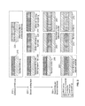
- FIGS. 1A-1C is a set of three drawings showing a thermally-conductive and mechanically-robust bonding method for attaching a metal nanowire (MNW) array to an adjacent surface.
- MNW metal nanowire
- FIG. 2 is a drawing showing a thermally-conductive and mechanically-robust bonding method for attaching a metal nanowire (MNW) array to an adjacent surface.
- MNW metal nanowire
- FIG. 3 is a flowchart of a thermally-conductive and mechanically-robust bonding method for attaching a metal nanowire (MNW) array to an adjacent surface.
- MNW metal nanowire
- FIG. 4 is a flowchart of a thermally-conductive and mechanically-robust bonding method for attaching a metal nanowire (MNW) array to an adjacent surface.
- MNW metal nanowire
- a thermally-conductive and mechanically-robust bonding procedure is provided to attach a metal nanowire (MNW) array to two adjacent surfaces.
- MNW metal nanowire
- a thin metallic bonding layer can be used to anchor the individual MNWs to the adjacent surface without compromising the mechanical properties of the MNW.
- a thickness of the metallic bonding layer is less than approximately 20% of one or more of the length of the MNW array and the height of the MNW array.
- metallically-bonded MNW MNWs may be implemented by infiltrating an interstitial volume of the MNW array with a bonding material and using adhesion of the bonding material to the adjacent surfaces as a method of attachment.
- the tip of each MNW can be metallically bonded to an adjacent surface using a process that in parallel bonds all of the MNWs in the array.
- a post MNW growth electrodeposition step can be used to deposit mushroom-like caps of bonding metal or alloy material onto the tips of the MNWs.
- the bonding cap can comprise one or more of a fusible metal and an alloy similar to a solder, a brazing agent or a diffusion bonding metal.
- An additional bonding layer is added at the top of the MNW.
- a bonding material can be deposited at the tip of the MNW to form a compound, segmented MNW.
- the segmented MNW is principally comprised of the conductive material while only a short section, less than 20% of the total MNW length located at the tip of the MNW is composed of the bonding material. If a slightly thicker bonding layer is desired, the electrodeposition of the bonding material can be continued until a continuous overplating layer of bonding material substantially covers the surface of one or more of the membrane and the MNW array.
- the conductive material comprises one or more of copper and silver.
- the bonding material is chosen based on the desired bonding process used. For example, one or more of a eutectic metal and a solder can be used for phase change bonding, where heating is applied to melt and adhere the molten bonding layer to the adjacent surface.
- the bonding material can be one or more of tin and gold and can be bonded using thermocompressive bonding.
- the bonding material comprises a polymer material.
- Other types of metallic bonding include brazing and welding, which can also be used to attach a bonding material at the MNW tips to an adjacent material.
- FIGS. 1A-1C is a set of three drawings showing a thermally-conductive and mechanically-robust bonding method for attaching a metal nanowire (MNW) array to an adjacent surface.
- MNW metal nanowire
- FIG. 1A following deposition and growth of the MNWs, the template membrane used in generating the MNWs is removed.
- the MNW array is then infiltrated with one or more of a fusible metal, an alloy, and a polymer resin, creating bondable material.
- the bondable material comprises molten material.
- the bondable material is wicked by capillary forces into an interstitial volume of the MNW array by capillary forces. Bonding material is then placed on an adjacent surface to the MNW.
- an adjacent surface is brought into contact with a top surface of the MNW while the bonding material is bondable.
- the bondable material comprises molten material.
- the bonding material is allowed to form a solid bond between the MNW and the adjacent surface. This process compresses one or more of the bonding material and the MNW array against the adjacent surface.
- An additional step may be performed of wetting the bonding material to the adjacent surface.
- FIG. 2 is a drawing showing a thermally-conductive and mechanically-robust bonding method for attaching a metal nanowire (MNW) array to an adjacent surface. The tips of an MNW array are bonded to an adjacent surface.
- MNW metal nanowire
- an MNW array is synthesized.
- the MNW array is grown to be either subfilled, where the length of the MNWs is less than the membrane thickness, as shown in step 215 , or filled to the top of the membrane such that the tips of the MNWs are even with the top surface of the membrane, as shown in step 220 . In either case, the membrane is left in place around the MNWs.
- a bonding layer is deposited onto the tips of the MNWs.
- This bonding layer can take one of three different forms. As shown in step 230 , if the MNW array is subfilled, a small amount of bonding material can be deposited directly onto the tip of each individual MNW, forming a short MNW segment of bonding material.
- step 235 if the MNW array is filled to the membrane thickness, a small amount of bonding material can be deposited onto the tip of each individual MNW, forming a small mushroom-cap of bonding material above each individual MNW.
- step 240 if the MNW array is filled to the membrane thickness, a large amount of bonding material can be deposited onto the surface of the array and membrane to form a continuous film of bonding material.
- step 250 the MNWs are bonded and the template membrane is removed.
- step 255 the template membrane is removed from the previously subfilled MNW array, and then in step 260 , the MNW array is bonded to the adjacent substrate.
- the MNW array is first bonded to the adjacent substrate.
- metallic bonding are solder/eutectic bonding, where the bonding material comprises one or more of a solder and a eutectic and where bonding is performed under heating and optional compression, and thermocompressive bonding, where the bonding material comprises one or more of tin and gold, and wherein bonding is performed under heating and compression.
- FIG. 3 is a flowchart of a thermally-conductive and mechanically-robust bonding method 300 for attaching a metal nanowire (MNW) array to an adjacent surface.
- MNW metal nanowire
- step 310 a template membrane is removed from the metal nanowire (MNW) array.
- Block 310 then transfers control to block 320 .
- step 320 a bonding material is placed on an adjacent surface to the MNW. Block 320 then transfers control to block 330 .
- step 330 the MNW is infiltrated with a bonding material.
- the step of infiltrating comprises heating the bonding material so that it becomes one or more of softened and molten.
- the step of infiltrating comprises chemically treating a composite material so as to create a bonding material. Block 330 then transfers control to block 340 .
- step 340 a surface adjacent to the MNW is brought into contact with a top surface of the MNW while the bonding material is bondable. Block 340 then transfers control to block 350 .
- Block 350 the bonding material is allowed to form a solid bond between the MNW and the adjacent surface. Block 350 then terminates the process.
- FIG. 4 is a flowchart of a thermally-conductive and mechanically-robust bonding method 400 for attaching a metal nanowire (MNW) array to an adjacent surface.
- MNW metal nanowire
- step 410 a bonding material is chosen based on a desired bonding process.
- Block 410 then transfers control to block 420 .
- step 420 without removing a metal nanowire (MNW) array from a template membrane, the bonding material is deposited onto a tip of the MNW. Block 420 then terminates the process.
- MNW metal nanowire
- Advantages of the invention include high thermal conductivity outside of the interfaces and formation of a cohesive joint between the two components.
- Embodiments of the invention minimize the thermal resistance between the MNW surface and the adjacent surface and provide long-lifetime adhesion that preserves its integrity under temperature gradients and thermal cycling.
- Fusible metal MNWs are used in applications where the mechanical stresses are comparatively low or for applications where the minimization of device temperature rise (or equivalently for high-heat flux devices) is the priority of the thermal design. For example, the mechanical stresses are less than approximately 20 megapascals (20 MPa).
- the resulting MNW must be comparatively thick since the bonding metal is stiff and mismatch in the coefficients of thermal expansion can cause the interface to fail.
- the MNWs provide both high thermal conductivity (greater than 20 watts per meter-kelvin [W/m-K]) and mechanical compliance.
- the mechanical compliance is between approximately 10 megapascals (MPa) and approximately 100 MPa.
- the mechanical compliance is between approximately 10 MPa and 1,000 MPa.
- the MNWs themselves provide the mechanical flexibility.
- the bond serves primarily to transfer heat between the surface and the MNW array and to maintain mechanical integrity of the interface.
Landscapes
- Chemical & Material Sciences (AREA)
- Engineering & Computer Science (AREA)
- Materials Engineering (AREA)
- Organic Chemistry (AREA)
- Metallurgy (AREA)
- Electrochemistry (AREA)
- Chemical Kinetics & Catalysis (AREA)
- Mechanical Engineering (AREA)
- Nanotechnology (AREA)
- Physics & Mathematics (AREA)
- General Physics & Mathematics (AREA)
- Crystallography & Structural Chemistry (AREA)
- Condensed Matter Physics & Semiconductors (AREA)
- Composite Materials (AREA)
- General Engineering & Computer Science (AREA)
- Thermal Sciences (AREA)
- Pressure Welding/Diffusion-Bonding (AREA)
- Manufacturing & Machinery (AREA)
- Die Bonding (AREA)
- Electroplating Methods And Accessories (AREA)
Abstract
A thermally-conductive and mechanically-robust bonding method for attaching a metal nanowire (MNW) array to an adjacent surface includes the steps of: removing a template membrane from the MNW; infiltrating the MNW with a bonding material; placing the bonding material on the adjacent surface; bringing an adjacent surface into contact with a top surface of the MNW while the bonding material is bondable; and allowing the bonding material to cool and form a solid bond between the MNW and the adjacent surface. A thermally-conductive and mechanically-robust bonding method for attaching a metal nanowire (MNW) array to an adjacent surface includes the steps of: choosing a bonding material based on a desired bonding process; and without removing the MNW from a template membrane that fills an interstitial volume of the MNW, depositing the bonding material onto a tip of the MNW.
Description
The present application claims the priority benefit of U.S. provisional patent application No. 62/121,010 filed Feb. 26, 2015 and entitled “Vertically Aligned Metal Nanowire Arrays and Composites for Thermal Management Applications,” the disclosure of which is incorporated herein by reference.
This application contains subject matter that is related to the subject matter of the following applications, which are assigned to the same assignee as this application. The below-listed U.S. Patent application is hereby incorporated herein by reference in its entirety:
“THERMAL INTERFACE MATERIALS USING METAL NANOWIRE ARRAYS AND SACRIFICAL TEMPLATES,” by Silverman, Starkovich, Peng, Tice, Barako, Coyan, and Goodson, filed on Jan. 26, 2016, U.S. Ser. No. 15/006,597.
A thermally-conductive and mechanically-robust bonding method for attaching a metal nanowire (MNW) array to an adjacent surface includes the steps of: removing a template membrane from the MNW; infiltrating the MNW with a bonding material; placing the bonding material on the adjacent surface; bringing an adjacent surface into contact with a top surface of the MNW while the bonding material is bondable; and allowing the bonding material to form a solid bond between the MNW and the adjacent surface.
A thermally-conductive and mechanically-robust bonding method for attaching a metal nanowire (MNW) array to an adjacent surface includes the steps of: choosing a bonding material based on a desired bonding process; and without removing the MNW from a template membrane to which the MNW is connected, depositing the bonding material onto a tips of the MNWs.
A metal nanowire (MNW) array includes: a vertically-aligned metal nanowire (MNW) array comprising a plurality of nanowires that grow upward from a seed layer deposited onto a template membrane, the template membrane being removed after MNW growth.
A metal nanowire (MNW) array includes a metal nanowire (MNW) array attached at the MNW tips to an adjacent surface by mushroom-like caps of thermally-conductive and mechanically-robust bonding material.
A metal nanowire (MNW) array includes a metal nanowire (MNW) array attached at the MNW tips to a continuous overplating layer of bonding material covers the template membrane.
The accompanying drawings provide visual representations which will be used to more fully describe various representative embodiments and can be used by those skilled in the art to better understand the representative embodiments disclosed herein and their inherent advantages. In these drawings, like reference numerals identify corresponding elements.
While the present invention is susceptible of embodiment in many different forms, there is shown in the drawings and will herein be described in detail one or more specific embodiments, with the understanding that the present disclosure is to be considered as exemplary of the principles of the invention and not intended to limit the invention to the specific embodiments shown and described.
A thermally-conductive and mechanically-robust bonding procedure is provided to attach a metal nanowire (MNW) array to two adjacent surfaces.
A thin metallic bonding layer can be used to anchor the individual MNWs to the adjacent surface without compromising the mechanical properties of the MNW. For example, a thickness of the metallic bonding layer is less than approximately 20% of one or more of the length of the MNW array and the height of the MNW array.
According to embodiments of the invention, metallically-bonded MNW MNWs may be implemented by infiltrating an interstitial volume of the MNW array with a bonding material and using adhesion of the bonding material to the adjacent surfaces as a method of attachment.
Alternatively, the tip of each MNW can be metallically bonded to an adjacent surface using a process that in parallel bonds all of the MNWs in the array. For example, while the MNWs are still in the membrane, a post MNW growth electrodeposition step can be used to deposit mushroom-like caps of bonding metal or alloy material onto the tips of the MNWs. The bonding cap can comprise one or more of a fusible metal and an alloy similar to a solder, a brazing agent or a diffusion bonding metal. An additional bonding layer is added at the top of the MNW.
If the MNWs are not grown to substantially extend to the full thickness of the membrane, then a bonding material can be deposited at the tip of the MNW to form a compound, segmented MNW. The segmented MNW is principally comprised of the conductive material while only a short section, less than 20% of the total MNW length located at the tip of the MNW is composed of the bonding material. If a slightly thicker bonding layer is desired, the electrodeposition of the bonding material can be continued until a continuous overplating layer of bonding material substantially covers the surface of one or more of the membrane and the MNW array. For example, the conductive material comprises one or more of copper and silver.
The bonding material is chosen based on the desired bonding process used. For example, one or more of a eutectic metal and a solder can be used for phase change bonding, where heating is applied to melt and adhere the molten bonding layer to the adjacent surface. Alternatively, the bonding material can be one or more of tin and gold and can be bonded using thermocompressive bonding. Alternatively, the bonding material comprises a polymer material. Other types of metallic bonding include brazing and welding, which can also be used to attach a bonding material at the MNW tips to an adjacent material.
In FIG. 1A , following deposition and growth of the MNWs, the template membrane used in generating the MNWs is removed.
In FIG. 1B , the MNW array is then infiltrated with one or more of a fusible metal, an alloy, and a polymer resin, creating bondable material. For example, the bondable material comprises molten material. For example, the bondable material is wicked by capillary forces into an interstitial volume of the MNW array by capillary forces. Bonding material is then placed on an adjacent surface to the MNW.
In FIG. 1C , an adjacent surface is brought into contact with a top surface of the MNW while the bonding material is bondable. For example, the bondable material comprises molten material. The bonding material is allowed to form a solid bond between the MNW and the adjacent surface. This process compresses one or more of the bonding material and the MNW array against the adjacent surface.
An additional step (not pictured) may be performed of wetting the bonding material to the adjacent surface.
In step 210, an MNW array is synthesized. The MNW array is grown to be either subfilled, where the length of the MNWs is less than the membrane thickness, as shown in step 215, or filled to the top of the membrane such that the tips of the MNWs are even with the top surface of the membrane, as shown in step 220. In either case, the membrane is left in place around the MNWs.
In step 225, a bonding layer is deposited onto the tips of the MNWs. This bonding layer can take one of three different forms. As shown in step 230, if the MNW array is subfilled, a small amount of bonding material can be deposited directly onto the tip of each individual MNW, forming a short MNW segment of bonding material.
As shown in step 235, if the MNW array is filled to the membrane thickness, a small amount of bonding material can be deposited onto the tip of each individual MNW, forming a small mushroom-cap of bonding material above each individual MNW.
As shown in step 240, if the MNW array is filled to the membrane thickness, a large amount of bonding material can be deposited onto the surface of the array and membrane to form a continuous film of bonding material.
In step 250, the MNWs are bonded and the template membrane is removed.
In step 255, the template membrane is removed from the previously subfilled MNW array, and then in step 260, the MNW array is bonded to the adjacent substrate.
In step 265, for the embodiments with bonding layer caps or with bonding layer overplating, the MNW array is first bonded to the adjacent substrate. The most common types of metallic bonding are solder/eutectic bonding, where the bonding material comprises one or more of a solder and a eutectic and where bonding is performed under heating and optional compression, and thermocompressive bonding, where the bonding material comprises one or more of tin and gold, and wherein bonding is performed under heating and compression.
In step 270, the template membrane is removed from the MNW array, FIG. 3 is a flowchart of a thermally-conductive and mechanically-robust bonding method 300 for attaching a metal nanowire (MNW) array to an adjacent surface.
In step 310, a template membrane is removed from the metal nanowire (MNW) array. Block 310 then transfers control to block 320.
In step 320 a bonding material is placed on an adjacent surface to the MNW. Block 320 then transfers control to block 330.
In step 330 the MNW is infiltrated with a bonding material. For example, the step of infiltrating comprises heating the bonding material so that it becomes one or more of softened and molten. For example, the step of infiltrating comprises chemically treating a composite material so as to create a bonding material. Block 330 then transfers control to block 340.
In step 340, a surface adjacent to the MNW is brought into contact with a top surface of the MNW while the bonding material is bondable. Block 340 then transfers control to block 350.
In block 350, the bonding material is allowed to form a solid bond between the MNW and the adjacent surface. Block 350 then terminates the process.
In step 410, a bonding material is chosen based on a desired bonding process. Block 410 then transfers control to block 420.
In step 420, without removing a metal nanowire (MNW) array from a template membrane, the bonding material is deposited onto a tip of the MNW. Block 420 then terminates the process.
Advantages of the invention include high thermal conductivity outside of the interfaces and formation of a cohesive joint between the two components. Embodiments of the invention minimize the thermal resistance between the MNW surface and the adjacent surface and provide long-lifetime adhesion that preserves its integrity under temperature gradients and thermal cycling. Fusible metal MNWs are used in applications where the mechanical stresses are comparatively low or for applications where the minimization of device temperature rise (or equivalently for high-heat flux devices) is the priority of the thermal design. For example, the mechanical stresses are less than approximately 20 megapascals (20 MPa).
Fusible metals undergo a phase change during bonding and can provide direct adhesion to adjacent surfaces. However, the resulting MNW must be comparatively thick since the bonding metal is stiff and mismatch in the coefficients of thermal expansion can cause the interface to fail. In vertically-aligned MNWs, the MNWs provide both high thermal conductivity (greater than 20 watts per meter-kelvin [W/m-K]) and mechanical compliance. For example, the mechanical compliance is between approximately 10 megapascals (MPa) and approximately 100 MPa. For example, the mechanical compliance is between approximately 10 MPa and 1,000 MPa. The MNWs themselves provide the mechanical flexibility. The bond serves primarily to transfer heat between the surface and the MNW array and to maintain mechanical integrity of the interface.
While the above representative embodiments have been described with certain components in exemplary configurations, it will be understood by one of ordinary skill in the art that other representative embodiments can be implemented using different configurations and/or different components. For example, it will be understood by one of ordinary skill in the art that the time horizon can be adapted in numerous ways while remaining within the invention.
The representative embodiments and disclosed subject matter, which have been described in detail herein, have been presented by way of example and illustration and not by way of limitation. It will be understood by those skilled in the art that various changes may be made in the form and details of the described embodiments resulting in equivalent embodiments that remain within the scope of the invention. It is intended, therefore, that the subject matter in the above description shall be interpreted as illustrative and shall not be interpreted in a limiting sense.
Claims (1)
1. A metal nanowire (MNW) array attached at MNW tips to a surface adjacent to the MNW array by thermally-conductive phase change bonding material filling a template membrane on top of the MNW array, wherein the MNW array is partially subfilled within the template membrane, the bonding material consisting of tin, the MNW array consisting of one or more of copper and silver.
Priority Applications (1)
| Application Number | Priority Date | Filing Date | Title |
|---|---|---|---|
| US15/422,602 US10180288B2 (en) | 2015-02-26 | 2017-02-02 | High-conductivity bonding of metal nanowire arrays |
Applications Claiming Priority (4)
| Application Number | Priority Date | Filing Date | Title |
|---|---|---|---|
| US201562121010P | 2015-02-26 | 2015-02-26 | |
| US15/006,658 US9468989B2 (en) | 2015-02-26 | 2016-01-26 | High-conductivity bonding of metal nanowire arrays |
| US15/249,535 US9601452B2 (en) | 2015-02-26 | 2016-08-29 | High-conductivity bonding of metal nanowire arrays |
| US15/422,602 US10180288B2 (en) | 2015-02-26 | 2017-02-02 | High-conductivity bonding of metal nanowire arrays |
Related Parent Applications (1)
| Application Number | Title | Priority Date | Filing Date |
|---|---|---|---|
| US15/249,535 Division US9601452B2 (en) | 2015-02-26 | 2016-08-29 | High-conductivity bonding of metal nanowire arrays |
Publications (2)
| Publication Number | Publication Date |
|---|---|
| US20170146302A1 US20170146302A1 (en) | 2017-05-25 |
| US10180288B2 true US10180288B2 (en) | 2019-01-15 |
Family
ID=55410251
Family Applications (3)
| Application Number | Title | Priority Date | Filing Date |
|---|---|---|---|
| US15/006,658 Active - Reinstated US9468989B2 (en) | 2015-02-26 | 2016-01-26 | High-conductivity bonding of metal nanowire arrays |
| US15/249,535 Active US9601452B2 (en) | 2015-02-26 | 2016-08-29 | High-conductivity bonding of metal nanowire arrays |
| US15/422,602 Active US10180288B2 (en) | 2015-02-26 | 2017-02-02 | High-conductivity bonding of metal nanowire arrays |
Family Applications Before (2)
| Application Number | Title | Priority Date | Filing Date |
|---|---|---|---|
| US15/006,658 Active - Reinstated US9468989B2 (en) | 2015-02-26 | 2016-01-26 | High-conductivity bonding of metal nanowire arrays |
| US15/249,535 Active US9601452B2 (en) | 2015-02-26 | 2016-08-29 | High-conductivity bonding of metal nanowire arrays |
Country Status (4)
| Country | Link |
|---|---|
| US (3) | US9468989B2 (en) |
| JP (2) | JP2018512279A (en) |
| TW (1) | TWI700139B (en) |
| WO (1) | WO2016137711A1 (en) |
Cited By (1)
| Publication number | Priority date | Publication date | Assignee | Title |
|---|---|---|---|---|
| US11229090B2 (en) | 2019-05-10 | 2022-01-18 | Northrop Grumman Systems Corporation | Multilayered nanowire arrays with lateral interposers |
Families Citing this family (7)
| Publication number | Priority date | Publication date | Assignee | Title |
|---|---|---|---|---|
| KR20190068176A (en) * | 2017-12-08 | 2019-06-18 | 삼성전자주식회사 | Method of forming nanorod structure and method of forming semiconductor device using the same |
| US10833048B2 (en) | 2018-04-11 | 2020-11-10 | International Business Machines Corporation | Nanowire enabled substrate bonding and electrical contact formation |
| US10446466B1 (en) | 2018-05-03 | 2019-10-15 | Raytheon Company | Mechanically improved microelectronic thermal interface structure for low die stress |
| US10971423B2 (en) * | 2018-06-08 | 2021-04-06 | Carnegie Mellon University | Metal nanowire based thermal interface materials |
| US11493288B2 (en) * | 2018-06-08 | 2022-11-08 | Carnegie Mellon University | Nanowire-based thermal interface |
| US11387202B2 (en) | 2019-03-01 | 2022-07-12 | Invensas Llc | Nanowire bonding interconnect for fine-pitch microelectronics |
| US11195811B2 (en) * | 2019-04-08 | 2021-12-07 | Texas Instruments Incorporated | Dielectric and metallic nanowire bond layers |
Citations (3)
| Publication number | Priority date | Publication date | Assignee | Title |
|---|---|---|---|---|
| US5367282A (en) * | 1992-07-21 | 1994-11-22 | Texas Instruments Incorporated | Electric motor protector sensor |
| JP2004128103A (en) | 2002-10-01 | 2004-04-22 | Toshiba Corp | Coil parts |
| US20050211461A1 (en) * | 2004-01-30 | 2005-09-29 | Hitachi Cable, Ltd. | Flat cable conductor, method of making the same and flat cable using the same |
Family Cites Families (53)
| Publication number | Priority date | Publication date | Assignee | Title |
|---|---|---|---|---|
| US6231744B1 (en) * | 1997-04-24 | 2001-05-15 | Massachusetts Institute Of Technology | Process for fabricating an array of nanowires |
| US7109581B2 (en) | 2003-08-25 | 2006-09-19 | Nanoconduction, Inc. | System and method using self-assembled nano structures in the design and fabrication of an integrated circuit micro-cooler |
| US7112525B1 (en) * | 2003-12-22 | 2006-09-26 | University Of South Florida | Method for the assembly of nanowire interconnects |
| US7422696B2 (en) * | 2004-02-20 | 2008-09-09 | Northwestern University | Multicomponent nanorods |
| JP2005335054A (en) * | 2004-04-27 | 2005-12-08 | Japan Science & Technology Agency | Metal nanowire and manufacturing method thereof |
| TWI255466B (en) | 2004-10-08 | 2006-05-21 | Ind Tech Res Inst | Polymer-matrix conductive film and method for fabricating the same |
| US7371674B2 (en) * | 2005-12-22 | 2008-05-13 | Intel Corporation | Nanostructure-based package interconnect |
| US20070221917A1 (en) * | 2006-03-24 | 2007-09-27 | Chin Wee S | Method of preparing nanowire(s) and product(s) obtained therefrom |
| US20070277866A1 (en) * | 2006-05-31 | 2007-12-06 | General Electric Company | Thermoelectric nanotube arrays |
| JP4897360B2 (en) | 2006-06-08 | 2012-03-14 | ポリマテック株式会社 | Thermally conductive molded body and method for producing the same |
| US7786024B2 (en) * | 2006-11-29 | 2010-08-31 | Nanosys, Inc. | Selective processing of semiconductor nanowires by polarized visible radiation |
| EP2162910B1 (en) * | 2007-04-23 | 2013-06-12 | University College Cork-National University of Ireland, Cork | A thermal interface material |
| US7728525B2 (en) * | 2007-07-27 | 2010-06-01 | Osram Sylvania Inc. | Relamping circuit for battery powered ballast |
| US20090214848A1 (en) | 2007-10-04 | 2009-08-27 | Purdue Research Foundation | Fabrication of nanowire array composites for thermoelectric power generators and microcoolers |
| TW200935635A (en) * | 2008-02-15 | 2009-08-16 | Univ Nat Chiao Tung | Method of manufacturing nanometer-scale thermoelectric device |
| EP2849265B1 (en) * | 2008-02-22 | 2021-05-12 | Colorado State University Research Foundation | Lithium-ion battery |
| US8129001B2 (en) * | 2008-03-17 | 2012-03-06 | The Research Foundation Of State University Of New York | Composite thermal interface material system and method using nano-scale components |
| JP5146256B2 (en) | 2008-03-18 | 2013-02-20 | 富士通株式会社 | Sheet-like structure and manufacturing method thereof, and electronic device and manufacturing method thereof |
| DE102008015333B4 (en) * | 2008-03-20 | 2021-05-12 | Gsi Helmholtzzentrum Für Schwerionenforschung Gmbh | Nanowire structural element, process for its production, microreactor system and catalyst system |
| US8968820B2 (en) * | 2008-04-25 | 2015-03-03 | Nanotek Instruments, Inc. | Process for producing hybrid nano-filament electrodes for lithium batteries |
| KR101476424B1 (en) * | 2008-06-23 | 2014-12-29 | 서울반도체 주식회사 | Thermal interface material for semiconductor chip and method of forming the same |
| US8017498B2 (en) * | 2008-09-22 | 2011-09-13 | Intel Corporation | Multiple die structure and method of forming a connection between first and second dies in same |
| US8574710B2 (en) * | 2008-10-10 | 2013-11-05 | Nano Terra Inc. | Anti-reflective coatings comprising ordered layers of nanowires and methods of making and using the same |
| CN101760035B (en) * | 2008-12-24 | 2016-06-08 | 清华大学 | The using method of thermal interfacial material and this thermal interfacial material |
| US8814456B2 (en) * | 2009-02-19 | 2014-08-26 | S.C. Johnson & Son, Inc. | Applicator for automatically dispensing self-adhesive products |
| US8106510B2 (en) * | 2009-08-04 | 2012-01-31 | Raytheon Company | Nano-tube thermal interface structure |
| US9059344B2 (en) * | 2009-08-24 | 2015-06-16 | Shih-Ping Bob Wang | Nanowire-based photovoltaic energy conversion devices and related fabrication methods |
| WO2011028054A2 (en) * | 2009-09-03 | 2011-03-10 | 한국표준과학연구원 | Production method for a silicon nanowire array using a porous metal thin film |
| US8177878B2 (en) * | 2009-11-30 | 2012-05-15 | Infineon Technologies Ag | Bonding material with exothermically reactive heterostructures |
| US8524525B2 (en) * | 2010-01-25 | 2013-09-03 | The Board Of Trustees Of The Leland Stanford Junior University | Joined nanostructures and methods therefor |
| CN105206794B (en) * | 2010-03-03 | 2018-02-23 | 安普瑞斯股份有限公司 | Template electrode structure for position activity material |
| WO2012111837A1 (en) | 2011-02-14 | 2012-08-23 | Jnc Corporation | High-performance thermal interface films and methods thereof |
| WO2012114552A1 (en) * | 2011-02-23 | 2012-08-30 | ソニー株式会社 | Transparent electroconductive film, information input device, and electronic instrument |
| CN103493149B (en) * | 2011-04-28 | 2015-11-25 | 富士胶片株式会社 | Dispersion containing metal nanowires and conductive film |
| US8815151B2 (en) * | 2011-05-23 | 2014-08-26 | Carestream Health, Inc. | Metal ion catalysis of metal ion reduction, methods, compositions, and articles |
| WO2013043926A1 (en) * | 2011-09-20 | 2013-03-28 | The Regents Of The University Of California | Nanowire composite for thermoelectrics |
| JP5646424B2 (en) * | 2011-09-27 | 2014-12-24 | 株式会社東芝 | Transparent electrode laminate |
| KR20130070729A (en) * | 2011-12-20 | 2013-06-28 | 제일모직주식회사 | Transparent conductive films including metal nanowires and carbon nanotubes |
| CN104508758B (en) | 2012-03-01 | 2018-08-07 | 雷蒙特亚特特拉维夫大学有限公司 | Conducting nanowires film |
| US10483104B2 (en) * | 2012-03-30 | 2019-11-19 | Kabushiki Kaisha Toshiba | Method for producing stacked electrode and method for producing photoelectric conversion device |
| US20140024677A1 (en) * | 2012-04-09 | 2014-01-23 | Musc Foundation For Research Development | Methods for inducing mitochondrial biogenesis |
| US9920207B2 (en) * | 2012-06-22 | 2018-03-20 | C3Nano Inc. | Metal nanostructured networks and transparent conductive material |
| US9082930B1 (en) | 2012-10-25 | 2015-07-14 | Alphabet Energy, Inc. | Nanostructured thermolectric elements and methods of making the same |
| KR102104919B1 (en) * | 2013-02-05 | 2020-04-27 | 삼성전자주식회사 | Semiconductor package and method of manufacturing the same |
| US9601406B2 (en) * | 2013-03-01 | 2017-03-21 | Intel Corporation | Copper nanorod-based thermal interface material (TIM) |
| KR101391510B1 (en) * | 2013-03-19 | 2014-05-07 | 경희대학교 산학협력단 | Muliple transparent electrode comprising metal nano wire |
| JP6065724B2 (en) * | 2013-04-16 | 2017-01-25 | 富士通株式会社 | Sheet-like structure, electronic device, method for manufacturing sheet-like structure, and method for manufacturing electronic device |
| US20160072034A1 (en) * | 2013-05-21 | 2016-03-10 | The Regents Of The University Of California | Metals-semiconductor nanowire composites |
| US20150011763A1 (en) * | 2013-07-03 | 2015-01-08 | Carestream Health, Inc. | Surface modification of metal nanostructures |
| CN106488819B (en) * | 2014-06-20 | 2018-06-22 | 维洛3D公司 | Apparatus, system and method for three-dimensional printing |
| KR102238180B1 (en) * | 2014-08-05 | 2021-04-08 | 엘지디스플레이 주식회사 | Flexible display device and method of fabricating the same |
| KR102225511B1 (en) * | 2014-08-26 | 2021-03-08 | 삼성전자주식회사 | Aqueous compositions, methods of producing conductive thin films using the same and conductive thin films produced thereby, and electronic devices including the same |
| US9942979B2 (en) * | 2014-11-03 | 2018-04-10 | Samsung Electronics Co., Ltd. | Flexible printed circuit board |
-
2016
- 2016-01-26 US US15/006,658 patent/US9468989B2/en active Active - Reinstated
- 2016-02-03 TW TW105103614A patent/TWI700139B/en active
- 2016-02-04 JP JP2017545222A patent/JP2018512279A/en active Pending
- 2016-02-04 WO PCT/US2016/016603 patent/WO2016137711A1/en not_active Ceased
- 2016-08-29 US US15/249,535 patent/US9601452B2/en active Active
-
2017
- 2017-02-02 US US15/422,602 patent/US10180288B2/en active Active
-
2021
- 2021-02-05 JP JP2021017397A patent/JP7220732B2/en active Active
Patent Citations (3)
| Publication number | Priority date | Publication date | Assignee | Title |
|---|---|---|---|---|
| US5367282A (en) * | 1992-07-21 | 1994-11-22 | Texas Instruments Incorporated | Electric motor protector sensor |
| JP2004128103A (en) | 2002-10-01 | 2004-04-22 | Toshiba Corp | Coil parts |
| US20050211461A1 (en) * | 2004-01-30 | 2005-09-29 | Hitachi Cable, Ltd. | Flat cable conductor, method of making the same and flat cable using the same |
Cited By (2)
| Publication number | Priority date | Publication date | Assignee | Title |
|---|---|---|---|---|
| US11229090B2 (en) | 2019-05-10 | 2022-01-18 | Northrop Grumman Systems Corporation | Multilayered nanowire arrays with lateral interposers |
| US11800602B1 (en) | 2019-05-10 | 2023-10-24 | Northrop Grumman Systems Corporation | Multilayered metal nanowire array |
Also Published As
| Publication number | Publication date |
|---|---|
| TW201706063A (en) | 2017-02-16 |
| JP7220732B2 (en) | 2023-02-10 |
| US20160250710A1 (en) | 2016-09-01 |
| WO2016137711A1 (en) | 2016-09-01 |
| JP2018512279A (en) | 2018-05-17 |
| US9601452B2 (en) | 2017-03-21 |
| US20170146302A1 (en) | 2017-05-25 |
| US9468989B2 (en) | 2016-10-18 |
| TWI700139B (en) | 2020-08-01 |
| JP2021087996A (en) | 2021-06-10 |
| US20160372438A1 (en) | 2016-12-22 |
Similar Documents
| Publication | Publication Date | Title |
|---|---|---|
| US10180288B2 (en) | High-conductivity bonding of metal nanowire arrays | |
| US5681647A (en) | Anisotropic conductive film for microconnections | |
| US7023089B1 (en) | Low temperature packaging apparatus and method | |
| US8742600B2 (en) | Dual-phase intermetallic interconnection structure and method of fabricating the same | |
| US20160251769A1 (en) | Thermal interface materials using metal nanowire arrays and sacrificial templates | |
| TWI300619B (en) | Electronic device | |
| TW200915452A (en) | Stable gold bump solder connections | |
| US10943796B2 (en) | Semiconductor device assembly having a thermal interface bond between a semiconductor die and a passive heat exchanger | |
| US9589864B2 (en) | Substrate with embedded sintered heat spreader and process for making the same | |
| CN114999943B (en) | A microstructure array interconnection method and device bonding structure | |
| WO2004064120A2 (en) | Semiconductor package having non-ceramic based window frame | |
| TWI329350B (en) | Capacitor attachment method | |
| CN112103262B (en) | Method for controlling crystal orientation and microstructure of all-intermetallic compound micro-interconnection welding spot | |
| WO2013129279A1 (en) | Semiconductor device production method | |
| JP2557268B2 (en) | Device mounting method | |
| TW200903758A (en) | Semiconductor device and method of manufacturing the same | |
| JP6636465B2 (en) | Process for permanent joining of two members by transient liquid phase interdiffusion | |
| JPS6153851B2 (en) | ||
| US20090166852A1 (en) | Semiconductor packages with thermal interface materials | |
| JP2017518186A5 (en) | ||
| US4765528A (en) | Plating process for an electronic part | |
| CN112652601A (en) | Semiconductor device and method for manufacturing semiconductor device | |
| KR101214061B1 (en) | Method of manufacturing electric connecting structure using low price anisotropic conductive paste | |
| JP2013004894A (en) | Semiconductor junction structure and method of manufacturing the same | |
| TWI272885B (en) | Method for forming presolder bump on circuit board by translate plate technique |
Legal Events
| Date | Code | Title | Description |
|---|---|---|---|
| STCF | Information on status: patent grant |
Free format text: PATENTED CASE |
|
| MAFP | Maintenance fee payment |
Free format text: PAYMENT OF MAINTENANCE FEE, 4TH YEAR, LARGE ENTITY (ORIGINAL EVENT CODE: M1551); ENTITY STATUS OF PATENT OWNER: LARGE ENTITY Year of fee payment: 4 |